
Caractérisation des Défauts Profonds dans le Silicium ... · Pr. Chahdi Mohamed Professeur...
157
RÉPUBLIQUE ALGÉRIENNE DÉMOCRATIQUE ET POPULAIRE MINISTÈRE DE L ‟ ENSEIGNEMENT SUPÉRIEUR ET DE LA RECHERCHE SCIENTIFIQUE THÈSE Présenté à l‟ Université de BISKRA Faculté des Sciences Exactes, des Sciences de la Nature et de la Vie Département de Sciences de la Matière En vue de l‟obtention du diplôme de Doctorat en Physique Par Tibermacine Toufik Caractérisation des Défauts Profonds dans le Silicium Amorphe Hydrogéné et autres Semiconducteurs Photo-Actifs de type III-V par la Méthode de Photocourant Constant: CPM Soutenu le : 17/02/2011, devant le jury : Pr. Sengouga Nouredine Professeur Président Université de Biskra Pr. Amar Merazga Professeur Directeur de thèse Université de Taif, Arabie Saoudite. Pr. Chahdi Mohamed Professeur Examinateur Université de Batna Pr. Saidane Abdelkader Professeur Examinateur Université d‟Oran Pr. Aida Mohamed Salah Professeur Examinateur Université de Taibah, Arabie Saoudite. Dr. Ledra Mohamed M.C.(A) Examinateur Université de Biskra
Transcript of Caractérisation des Défauts Profonds dans le Silicium ... · Pr. Chahdi Mohamed Professeur...
RÉPUBLIQUE ALGÉRIENNE DÉMOCRATIQUE ET POPULAIRE
MINISTÈRE DE L‟ENSEIGNEMENT SUPÉRIEUR ET DE LA RECHERCHE SCIENTIFIQUE
THÈSE
Présenté à l‟Université de BISKRA
Faculté des Sciences Exactes, des Sciences de la Nature et de la Vie
Département de Sciences de la Matière
En vue de l‟obtention du diplôme de
Doctorat en Physique
Par
Tibermacine Toufik
Caractérisation des Défauts Profonds dans le Silicium Amorphe
Hydrogéné et autres Semiconducteurs Photo-Actifs de type III-V
par la Méthode de Photocourant Constant: CPM
Soutenu le : 17/02/2011, devant le jury :
Pr. Sengouga Nouredine Professeur Président Université de Biskra
Pr. Amar Merazga Professeur Directeur de thèse Université de Taif, Arabie
Saoudite.
Pr. Chahdi Mohamed Professeur Examinateur Université de Batna
Pr. Saidane Abdelkader Professeur Examinateur Université d‟Oran
Pr. Aida Mohamed Salah Professeur Examinateur Université de Taibah,
Arabie Saoudite.
Dr. Ledra Mohamed M.C.(A) Examinateur Université de Biskra
ii
AACCKKNNOOWWLLEEDDGGMMEENNTTSS
I am greatly indebted to Dr. Merazga Amar for supervising my Doctorat
thesis. He has offered me the occasion to realize the present thesis in
Laboratory of Metallic and Semiconducting Materials (LMSM) at University
of Biskra in Algeria. His advises and comments greatly helped me in my
scientific life.
I am glad that I could visit Epicenter laboratory at University of Dundee in
UK. I met there very freindly atmosphere. Especially, I wish to thank C. Main
and S. Reynolds for their hospitality during a research visit to Dundee
University where the CPM experiment has been done.
I am grateful to the Algerian Ministry of Higher Education and Research for
support.
I also thank my family who supported me during my postgraduate studies.
Last, but not least, I would like to thank all my colleagues from LMSM
laboratory, for fruitful cooperation and pleasant atmosphere at the laboratory.
iii
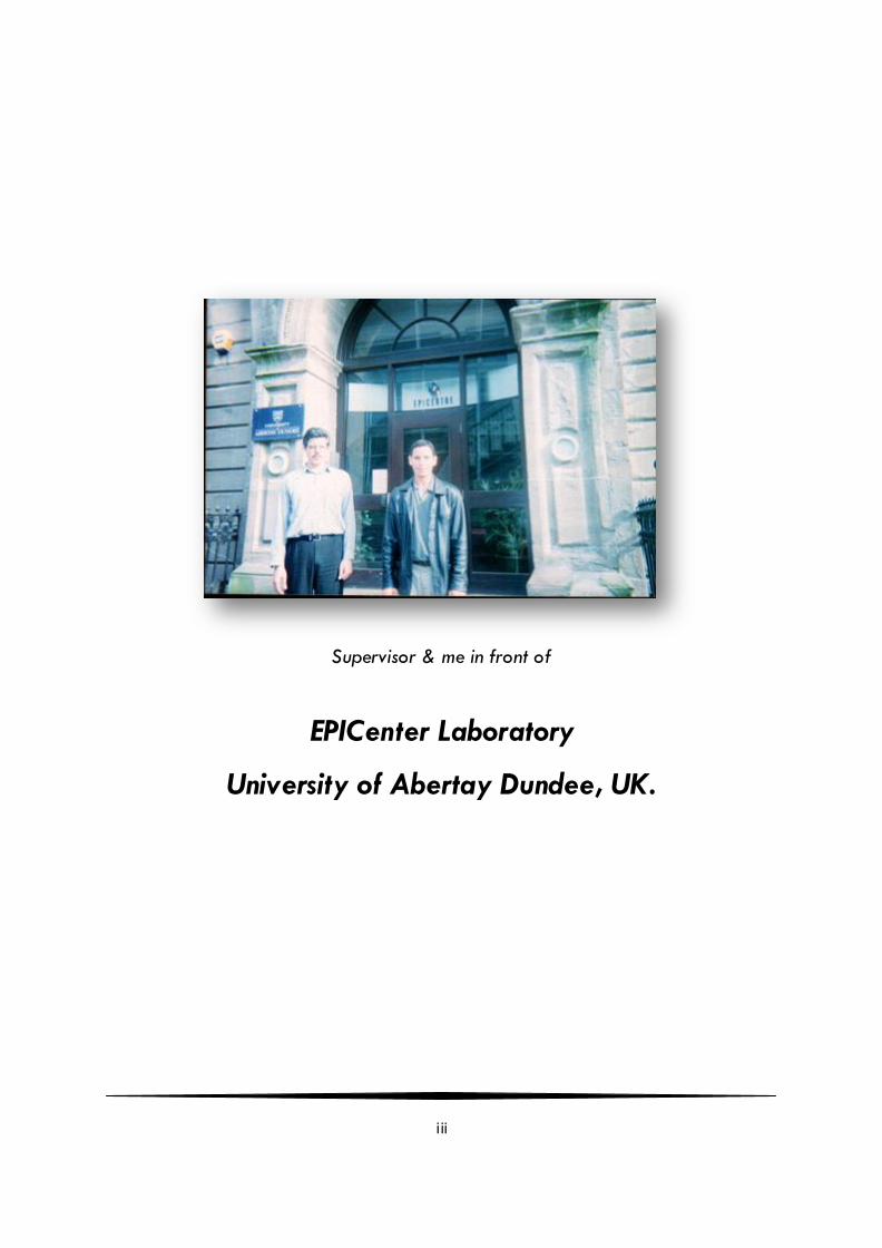
Supervisor & me in front of
EPICenter Laboratory
University of Abertay Dundee, UK.
iv
ملخصملخص
h
DOS
a-Si:Hc-Si:Hµ
(SI-GaAs:Cr
CPMDC-CPM
AC-CPM
„„gap‟‟
DCAC
AC
D-
Do
CPM DCAC
„„Defect Pool‟‟
DCAC
AC
a-Si:Hc-Si:HµSI-GaAs:Cr
DC-CPMAC-CPM
v
AABBSSTTRRAACCTT
We present in this thesis the optical and electronic properties of a number of semiconductor
materials namely undoped and P-doped hydrogenated amorphous silicon a-Si:H prepared by
Plasma Enhanced Chemical Vapour Deposition (PECVD), hydrogenated micro-crystalline
silicon (c-Si:H) prepared by Very High Frequency Plasma-Enhanced Chemical Vapor
Deposition (VHF-PECVD) and semi- insulating Cr-doped GaAs (SI-GaAs:Cr) prepared by the
Liquid Encapsulated Czochralski (LEC) method. Sub-band gap optical absorption spectra
(h) of all samples have been measured by the constant photocurrent technique in dc and ac
excitation (dc-CPM and ac-CPM). Then, these absorption coefficients are converted into
electronic density of states (DOS) distribution within the mobility gap by applying the
derivative method of Pierz et al. We present in this thesis the relationship between the optic al
excitation frequency and the optical and electronic properties of semiconductors materials in
particular a-Si:H, c-Si:H and GaAs.
We have developed a code program to simulate the dc and ac-CPM sub-band-gap optical
absorption spectra. This numerical simulation includes all possible thermal and optical
transitions between extended states and gap states. Our numerical results shows that (i) a
discrepancy between dc mode and ac mode in absorption spectrum and gap state distribution
particularly in defect region; (ii) extraction of DOS distribution using ac mode is better than
using dc mode specially at high frequency (iii) DOS distribution can be reasonably
reconstructed over a wide range of energy, especially at ultra high frequency, using both
n(h) p(h) corresponding to optical transitions associated with free electrons and free
holes creation, respectively. In addition and to validate our simulation results, we have
measured (h) for all samples at several frequencies. Our experimental results prove the
simulation ones and showed that a significant difference between dc- and ac-absorption
spectra is observed in defect region and that the determination of the density of the occupied
states within the gap mobility of the material is better for high frequencies than for low
frequencies. The evolution of the sub-band-gap absorption coefficient (h) and the CPM-
determined density of gap-states distribution within the gap versus the illumination time leads
to: (i) an increase in the deep defect absorption without any significant changes in the Urbach
tail (exponential part), (ii) a presence of more charged than neutral defects as predicted by the
vi
defect pool model, and (iii) a saturation point of the degradation of both optical absorption
coefficient and density of deep states of slightly P-doped sample measured by dc-CPM. The
constant photocurrent technique in dc-mode as a spectroscopy method for the defect
distribution determination is, therefore, most reliable to study the light soaking effect on the
stability of hydrogenated amorphous silicon layers used in solar cells manufacturing.
The constant photocurrent method in the ac-mode (ac-CPM) is also used in this work to
determine the defect density of states (DOS) in microcrystalline silicon (c-Si:H) and to
investigate the defect levels of semi- insulating Cr-doped GaAs from the optical absorption
spectrum. The microcrystalline absorption coefficient spectrum (h) is measured under ac-
CPM conditions at 60Hz and then is converted by the CPM spectroscopy into a DOS
distribution covering a portion in the lower energy range of occupied states. By deconvolution
of the measured optical absorption spectrum of SI-GaAs: Cr, we have extracted the
distribution of the deep defect states. Independently, computer simulations of the ac-CPM for
both materials are developed. Using a DOS model for microcrystalline which consistent with
the measured ac-CPM spectra and a previously measured transient photocurrent (TPC) for
the same material, the total ac-(h) is computed and found to agree satisfactorily with the
measured ac-(h). Using a DOS model for gallium arsenide which consistent with the
measured ac-CPM spectra and a previously measured modulated photocurrent (MPC) for the
same material, the total ac-(h) is computed and found to agree satisfactorily with the
measured ac-(h).The experimentally inaccessible components n(h) and p(h),
corresponding to optical transitions associated, respectively, with free electron and free hole
creation, are also computed for both semiconductors. The reconstructed DOS distributions in
the lower part of the energy-gap from n (h) and in the upper part of the energy-gap from p
(h) fit reasonably well the DOS model suggested by the measurements. The results are
consistent with a previous analysis, where the sub-gap ac-(h) saturates to a minimum
spectrum at sufficiently high frequency and the associated DOS distribution reflect reliably
and exclusively the optical transitions from low energy occupied states.
Keywords: a-Si:H; c-Si:H; SI-GaAs:Cr; ac-CPM; dc-CPM; Optical Absorption Spectrum;
Deep Defect Density; Light Soaking.
vii
RREESSUUMMEE
Le but de ce travail est de déterminer les propriétés optiques et électroniques en termes de
coefficient d‟absorption optique et densité d‟états électronique d‟un certain nombre de semi-
conducteurs à savoir le silicium amorphe hydrogéné (a-Si:H), silicium microcristallin (µc-
Si:H), arséniure de gallium dopé au chrome (SI-GaAs:Cr). Pour cette raison, on a mesuré le
coefficient d'absorption optique des échantillons par la méthode de photo-courant constant en
régime continu (DC-CPM) et en régime périodique (AC-CPM) pour plusieurs fréquences
d‟excitation optique. Ensuite on a convertit les spectres d‟absorption mesurés en densité
d'états électronique à l‟intérieure du gap de mobilité. Une différence est observée concernant
le coefficient d‟absorption optique et la densité d‟états profonds entre le régime périodique et
le régime continu d‟un coté et entre les différentes fréquences d‟un autre coté. On a aussi,
mesuré l‟évolution du coefficient d‟absorption et la distribution d'états électronique avec
l‟illumination. Cette mesure montre une augmentation de la densité de défauts profonds, une
présence de défauts chargés plus importante que les défauts neutre et une saturation pour des
temps d‟illuminations très longues. En outre, on a développé un programme pour modéliser la
technique CPM en mode DC et AC qui tient en compte toutes les transitions optiques
possibles. Notre modélisation nous a démontré l‟importance de considérer les deux
coefficients d‟absorption celles du aux électrons et celle due aux trous. Ceci est essentiel pour
reconstituer la distribution des états occupés et non occupés en utilisant ces deux coefficients
surtout pour des hautes fréquences. Au fur et à mesure que la fréquence augmente, les
propriétés optiques en termes de spectre d‟absorption optique sont plus en plus sous-estimées
quand aux propriétés électroniques en termes de densité d‟états électronique sont plus en plus
bien déterminées.
Mots clés : Spectre d‟absorption optique ; Densité des défauts profonds ; a-Si:H ; µc-Si :H ;
SI-GaAs :Cr ; AC-CPM ; DC-CPM ; Illumination Intense.
viii
TTAABBLLEE OOFF CCOONNTTEENNTTSS
Title i
Acknowledgements ii
Abstract v
Table of contents viii
Chapter 1. General introduction
1.1. Introduction 1
1.2. Background and Motivation 3
1.3. Objectives and outline of the thesis 6
References
Chapter 2. Introduction to amorphous semiconductors
2.1. Introduction 11
2.2. Fundamental properties of hydrogenated amorphous silicon 11
2.2.1. Structural properties 11
2.2.2. Electronic structure 18
2.2.3. Effects of doping 22
2.2.4. Metastability and Staebler-Wronski effect 24
2.2.5. Optical properties of a-Si:H 25
2.2.6. Mechanisms of transport 29
2.2.7. Phenomena of recombination 30
2.3. Fundamental properties of hydrogenated micro crystalline silicon 31
2.3.1. Deposition methods of hydrogenated micro crystalline silicon 31
2.3.2. Atomic structure 31
2.3.3. Electrical and optical properties 32
2.3.4. Advantages of μc-Si:H 33
References
ix
Chapter 3. Characterization techniques of amorphous semiconductors
3.1. Introduction 37
3.2. Dark conductivity 38
3.3. Steady state photoconductivity 40
3.4. Constant photocurrent measurement 44
3.5. Photothermal deflection spectroscopy 49
3.6. Dual beam photoconductivity 52
References
Chapter 4. Constant photocurrent technique: Theory and modeling
4.1. Introduction 57
4.2. Density of states distribution models for a-Si:H 57
4.3. Trapping and recombination 63
4.4. Absorption and generation 65
4.5. Function occupancy 70
4.5.1. Thermal equilibrium 70
4.5.2. Steady state equilibrium 71
4.5.3. Dynamic equilibrium 73
4.6. Implementation of numerical model 74
4.6.1. Steady state equilibrium: DC contribution 74
4.6.2. Dynamic equilibrium: AC contribution 76
4.6.3. Deconvolution procedure 78
References
x
Chapter 5. Constant photocurrent technique: Results and discussion
5.1. Introduction 81
5.2. Experimental procedure 82
5.3. Dark conductivity and activation energy measurements 85
5.4. Reflectance-Transmittance measurements 88
5.5. Optical absorption spectrum measurement: Constant Photocurrent Method 91
5.6. Density of states 95
5.7. Results and discussion 96
5.7.1. Hydrogenated amorphous silicon a-Si :H: Undoped sample Intersolar ISB4 96
5.7.2. Hydrogenated amorphous silicon a-Si :H: Doped sample : P272 104
5.7.3. Hydrogenated micro-crystalline silicon c-Si :H : OCC354 sample 109
5.7.4. Semi- insulating Cr doped Gallium arsenide :SI- GaAs :Cr sample 1713 117
5.7.5. Ultra high frequency effect 121
5.7.6. Light Soaking effect 123
References
Chapter 6. Summary and conclusions
6.1. Conclusions 129
6.2. Suggestions for further work 132
Appendix A 136
Appendix B 139
Appendix C 141
Appendix D 142
Appendix E 143
Appendix F 145
CHAPTER 1 GENERAL INTRODUCTION
1
CHAPTER 1
GENERAL INTRODUCTION
1.1. Introduction
Solar cell technology is an attractive alternative to conventional sources of electricity for it
provides non-polluting and renewable energy. Due to the dwindling supply of fossil fuels and
the environmental concerns, demand for new sources of energy is ever increasing worldwide.
Though solar cells hold the promise of clean and renewable source of energy, the cost aspect
of the solar cell technology has been a drawback to the wide-spread use of solar cells.
However, the recent advances in realizing a lower cost of solar cells will eventually lead to a
significant impact of solar cells on to the global energy market. In thin-film silicon solar cells,
the deposited silicon is a different phase compared to crystalline silicon c-Si: it is
hydrogenated amorphous silicon (a-Si:H) or hydrogenated microcrystalline silicon (μc-Si:H).
Most solar cells are made from single crystalline silicon. The production of single crystal
silicon cells is very costly and the cells made from it have several other factors that limit the
extent to which the costs can be further reduced. The absorptivity of single-crystal silicon is
very low requiring thick cells in order to achieve the required efficiency. This makes single-
crystalline cells rather expensive to produce.
Amorphous silicon may provide the answer to inexpensive production of solar cells. The
absorptivity of amorphous silicon is far greater than that of single-crystal silicon. Therefore,
a-Si:H solar cells can be made very thin d ~0.5 μm. The other advantages of amorphous
silicon solar cells is the extreme abundance of the raw material from which they can be made
and the low fabrication temperatures which facilitate the use of a variety of low-cost
substrates. Based on this concept, in 1976 the first experimental a-Si:H p-i-n solar cell was
made by Carlson and Wronski with an energy conversion efficiency of 2.4%. Nowadays, such
cells can be made with initial conversion efficiencies η greater than 10%.
CHAPTER 1 GENERAL INTRODUCTION
2
The drawback of amorphous silicon based solar cells is that their efficiencies appear to be
considerably less than their crystalline counterparts. Another problem is that amorphous
silicon suffers from light induced metastable effects known as Staebler-Wronski effect
(SWE). This means that upon illumination the material degrades over time, reducing the
percentage of light that can be converted to electricity. Despite this drawback, the low cost of
this material and the attractiveness of large area production still makes amorphous silicon
ideally suited for low cost solar cells. The improvements in the stabilized efficiency of a-Si:H
have been achieved mostly through material improvements, adopted cell designs and light
trapping techniques. This still leaves many fundamental questions unanswered regarding the
growth and material properties of amorphous silicon as well as the electronic characterist ics
of the solar cells.
Recently, hydrogenated microcrystalline silicon (µc-Si:H) has attracted much interest for
being used in optoelectronic applications. As compared to hydrogenated amorphous silicon
(a-Si:H), it offers a higher stability against light and current induced degradation and a wider
absorption bandwidth extending into the near infrared. In 1992 Faraji et al. reported a thin-
film silicon solar cell with a μc-Si:H:O i- layer. The first solar cell with a μc-Si:H i- layer was
reported in 1994 by Meier et al. at IMT Neuchˆatel, Switzerland with η = 4.6%. In the
following years, at this institute the concept of “micromorph” tandem cells was developed: a
tandem with a microcrystalline bottom cell and an amorphous top cell. In 2002, Meier et al.
published a micromorph tandem with η = 10.8% stable (12.3% initial) of which the bottom
cell (thickness of d = 2 μm) was deposited at a rate of rd = 0.5 nm/s. The highest initial
efficiency of 14.7% was reported by Yamamoto et al. of Kaneka, Japan. Because of the fact
that not only the efficiency but also the manufacturing costs of the solar cell determine the
feasibility as an industrial product, the trend in research has moved towards higher deposition
rates, while reducing the loss in material properties and cell performance to a minimum.
Further development and optimization of a-Si:H/μc-Si:H tandems will remain very important
because it is expected that in the near future (first half of this century) its market share will be
considerable. For example, in the European Roadmap for PV R&D, it is predicted that in
2020 the European market share for thin-film silicon (most probably mainly a-Si:H/μc-Si:H
tandems) will be 30%. This shows the importance of second generation solar cells.
CHAPTER 1 GENERAL INTRODUCTION
3
1.2. Background and Motivation
One of the central issues of the physics of amorphous solids is the nature of the band tails in
the electronic density of states (DOS). Particular issues include the following: (i) what is the
origin of the exponential shape of the tails seen in optical absorption measurements? (ii) How
does the spatial character of the electronic eigenstates change from the highly local midgap
states to the extended states interior to the valence or conduction bands? The nature of the
electronic states for electron energies ranging between midgap ( localized) to valence or
conduction (extended) is of obvious interest to the theory of doping and transport.
Hydrogenated amorphous silicon (a-Si :H)
Hydrogenated amorphous silicon (a-Si:H) was discovered by Chittick et al in 1969 and the
possibility of doping was demonstrated by Spear and LeComber in 1975. Since then,
hydrogenated amorphous silicon is extensively used in diverse optoelectronic applicat ions.
This material is nowadays used for sensors, for thin film transistors, and not in the least for
solar cells. a-Si:H has particular properties such as adjustable gap mobility by combining it
with nitrogen, carbon or germanium, direct band gap, absorption in the visible wavelength
region is about 100 times higher than that of crystalline silicon, easy to prepare on glass
substrates and at low temperatures, can be directly produced in a form that can cover a very
large area.
Hydrogenated amorphous silicon is the non-crystalline form of silicon. In the crystalline state,
the atoms form a periodic array with each one bonded to four others; the bond lengths and
angles are similar for each atom and long range order exists. In the amorphous state, the long
range order does not exist. There is, however, still short-range order, i.e., most silicon atoms
have four neighbors in a nearly diamond like structure. As a result of the short-range order,
a-Si:H has a band structure and the common semiconductor concept o f conduction and
valence bands can be used. However, the absence of long-range order means that these bands
are not sharp and have tails that extent into the band gap. Physically these band tails represent
energy levels of strained silicon-silicon bonds, resulting from bond-angle and/or bond- length
distributions. The width of these band tails is more or less a measure for the amount of
disorder in the material. In addition to the band tails there is a quasi-continuum of states
throughout the band tails related to broken bonds, usually referred to as dangling bonds.
CHAPTER 1 GENERAL INTRODUCTION
4
These dangling bonds can capture charge carriers and have three charge states: the D- has two
electrons, the Do has one electron and the D+ has no electrons. Fortunately most of these
dangling bonds are passivated by hydrogen that is incorporated most commonly through the
process of Plasma Enhanced Chemical Vapor Deposition (PECVD) and hence the dangling
bonds density is reduced from about 1021 cm-3 in pure amorphous silicon (a-Si) to 1015 cm-3,
i.e., less than 1 dangling bond per million atoms. Although hydrogenated amorphous silicon
contains more hydrogen than defects, still not all the defects are passivated. Presently, the
general agreement is that there is equilibrium between the width of the tail states (i.e., the
density of weak or strained Si-Si bonds) and the defect density. Unfortunately, D. Staebler
and C. Wronski discovered, more than 30 years ago, the degradation of the electronic
properties of a-Si:H under prolonged illumination by an intense light. Even at moderate light
intensities (e.g., by exposure to sunshine), the dark conductivity and photoconductivity can be
significantly reduced. This Staebler-Wronski effect increase the number of dangling bonds
through a mechanism for the breaking of weak Si-Si bonds from less than 1016 cm-1 in as
deposited intrinsic layers to about 1017 cm-1 in degraded layers.
Hydrogenated microcrystalline silicon (µc-Si:H)
Hydrogenated microcrystalline silicon (µc-Si:H) appears to be a more stable alternative.
µc-Si:H was first reported by Veˇprek et al. in Europe in 1968 and in Japan by Matsuda et al.
and Hamasaki et al. in 1980. The electronic properties and performance of c-Si:H films are
correlated with the deposition parameters and the structural properties. It is in fact
heterogeneous in nature, which leads to difficulties in the explanation of its electronic
transport properties. Therefore, the detailed knowledge of the gap density of states (DOS) in
µc-Si:H is of great importance to understand the transport mechanism. However, as µc-Si:H is
a phase mixture of crystalline and amorphous regions separated by grain boundaries and
voids, little is known about the nature and the energy distribution of the DOS. It is therefore
not surprising if there exists no conclusive DOS map and the understanding does not go in
many cases beyond a phenomenological description. In contrast to crystalline silicon, the
presence of band-tail states and deep defects opens additional transport paths that might act as
traps or form barriers for charge carriers. There is a wide range of possible structures in µc-
Si:H material which explain the large spread in reported drift mobilities and transport
CHAPTER 1 GENERAL INTRODUCTION
5
properties, but the similarity between µc-Si:H and a-Si:H suggest that structural disorder is
common feature and transport in µc-Si:H might take place by trap- limited band motion
(multiple trapping) or by direct tunneling between localized states (hopping) at low
temperature.
Constant Photocurrent Method: CPM
The tail states and the dangling bonds have a large effect on the electronic and optical
properties of amorphous semiconductors. Sub-band gap absorption coefficient of these
materials can provide useful information on their electronic transport and optical properties. It
can be used to infer the spectral distribution of the density of gap states of such materials.
Many sub-band gap absorption spectroscopy methods have been applied in order to determine
DOS but the sensitivity of each technique is not the same in the different regions of the band
gap. The most extensive are the constant photocurrent method (CPM), the photo-thermal
deflection spectroscopy (PDS) and the dual beam photoconductivity (DBP) which have been
used to evaluate the DOS in the lower energy range of the band gap near the valence band,
whereas the transient photoconductivity (TPC) and the modulated photocurrent (MPC) have
been used to determine the DOS in the upper energy range of the gap, close to the conduction
band.
The constant photocurrent method was originally developed for crystalline semiconductors
and then applied to amorphous materials by Vanecek et al. in 1981. CPM is one of the sub–
band gap absorption measurements used to characterise N-type, intrinsic or P-type a-Si:H
materials. By means of this optical spectroscopy method we can measure the sub-band gap
optical absorption spectrum of amorphous semiconductor using steady (dc-CPM) or
modulated (ac-CPM) sub-gap illumination. This latter gives us access to the density of states
since photons can excite electrons from filled defect states to the conduction band or from the
valence band to the empty defect states. Unfortunately, this technique is based on a number of
assumptions, causing its applicability and validity to have often been questioned. Bube et al.
noted that to determine the midgap defect densities the dc-CPM have to be corrected. Mettler
et al. concluded that there is a “working point” at which the basic CPM conditions are
fulfilled. Zhang et al. found that an inhomogeneous spatial distribution of defects have a
strong influence on the CPM determined defect density. Schmidt et al. reported that the
CHAPTER 1 GENERAL INTRODUCTION
6
absorption coefficient measured with dc-CPM is dependent on the constant photocurrent
chosen to perform the measurement. The constant photocurrent method can be also performed
in the ac mode where the sub-band-gap excitation light is chopped at different frequencies.
Nevertheless, discrepancies between the dc and ac modes have been observed and studied by
several authors. Conte et al. reported the discrepancy between measurements by dc and ac-
CPM and also observed experimentally the dependence of the dc-CPM spectra on the
magnitude of the adopted constant photocurrent. Sládek and Thèye found that the difference
between dc and ac measurements results by the fact that the response time of the photocurrent
is too slow and reduces with photon energy at room temperature since the difference
disappear at low temperatures. Hasegawa et al. found this difference and concluded that the
response time increase for low value of h. Main et al. in recent work explained this
discrepancies in terms of the relative contribution of phonon assisted transitions in the
generation process. Following these different interpretations, one can conclude that the
subject is still open to discussion and needs more explanations.
1.3. Objectives and outline of the thesis
Defect levels in semiconductor band gaps determine the electrical and optical properties
devices. These properties are determined by the relative position of the level and the capture
cross section of the carriers. The defect levels can capture minority, majority carriers or both
carriers for the deep states in this case they act as recombination centers. Capture and
emission of majority and minority carriers at defect levels in semiconductors materials are
characterized, most usually, by DLTS and MCTS. For semi- insulating (SI) crystals like GaAs
and amorphous materials like a-Si:H and c-Si:H other techniques must be used such as TPC,
MPC and CPM.
On the simulation side, great effort was deployed to model the TPC in a-Si:H and c-Si:H,
while modeling has been less employed to elucidate the experimental results of the CPM
technique in a-Si:H and c-Si:H, particularly in the ac mode.
In a previous ac-CPM analysis, Main et al demonstrate that the ac-CPM may be more reliable
than the dc-CPM in probing the DOS distribution in disordered semiconductors in the energy
range of occupied states below the Fermi- level. In this analysis, the electron transitions fall
into two categories, the direct optical transitions from occupied states be low the Fermi- level
CHAPTER 1 GENERAL INTRODUCTION
7
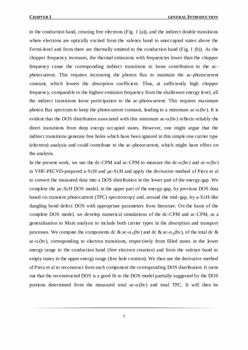
to the conduction band, creating free electrons (Fig. 1 (a)), and the indirect double transitions
where electrons are optically excited from the valence band to unoccupied states above the
Fermi- level and from there are thermally emitted to the conduction band (Fig. 1 (b)). As the
chopper frequency increases, the thermal emissions with frequencies lower than the chopper
frequency cause the corresponding indirect transitions to loose contribution to the ac-
photocurrent. This requires increasing the photon flux to maintain the ac-photocurrent
constant, which lowers the absorption coefficient. Thus, at sufficiently high chopper
frequency, comparable to the highest emission frequency from the shallowest energy level, all
the indirect transitions loose participation to the ac-photocurrent. This requires maximum
photon flux spectrum to keep the photocurrent constant, leading to a minimum ac-(h). It is
evident that the DOS distribution associated with this minimum ac-(h) reflects reliably the
direct transitions from deep energy occupied states. However, one might argue that the
indirect transitions generate free holes which have been ignored in this simple one carrier type
(electron) analysis and could contribute to the ac-photocurrent, which might have effect on
the analysis.
In the present work, we use the dc-CPM and ac-CPM to measure the dc-(h) and ac-(h)
in VHF-PECVD-prepared a-Si:H and µc-Si:H and apply the derivative method of Pierz et al
to convert the measured data into a DOS distribution in the lower part of the energy-gap. We
complete the µc-Si:H DOS model, in the upper part of the energy-gap, by previous DOS data
based on transient photocurrent (TPC) spectroscopy and, around the mid-gap, by a-Si:H- like
dangling bond defect DOS with appropriate parameters from literature. On the basis of the
complete DOS model, we develop numerical simulations of the dc-CPM and ac-CPM, as a
generalisation to Main analysis to include both carrier types in the absorption and transport
processes. We compute the components dc & ac-n(h) and dc & ac-p(h), of the total dc &
ac-(h), corresponding to electron transitions, respectively from filled states in the lower
energy range to the conduction band (free electron creation) and from the valence band to
empty states in the upper energy range (free hole creation). We then use the derivative method
of Pierz et al to reconstruct from each component the corresponding DOS distribution. It turns
out that the reconstructed DOS is a good fit to the DOS model partially suggested by the DOS
portions determined from the measured total ac-(h) and total TPC. It will then be
CHAPTER 1 GENERAL INTRODUCTION
8
concluded that the measured ac-(h) is mainly due to direct optical transitions of the
electrons occupying the defect states in the lower half of the gap.
Figure 1. Two optical transition categories according to Main ac-CPM analysis:
(a) Direct transitions creating free electrons (●) with rate Gn(E,h).
(b) Indirect double transitions creating free holes (○): an optical transition from the valence band
to an empty state at E above EF, with rate Gp(E,h), followed by a thermal transition from E
to the conduction band with rate Ten(E).
In this thesis, we combines experimental and computer modeling studies aimed at
understanding the difference between two modes dc and ac-CPM of amorphous silicon
,microcrystalline silicon and III-V semiconductors particularly SI GaAs Cr doped. The scope
of the thesis encompasses the application of the microscopic models describing the
distribution of midgap defect states to numerical simulations of the optical absorption
coefficient of a set of semiconductors. We have developed computer modeling schemes for
simulating the CPM technique of amorphous and microcrystalline silicon films taking into
account the nature and distributions of dangling bond states depicted by defect pool model.
Specific research objectives of this thesis therefore include (1) experimental understanding of
constant photocurrent measurements in the steady and periodic regime of several
semiconductors materials ; (2) development of a simulation technique for CPM experiment
taking into account all possible optical and thermal transitions between localized and
extended states ; (3) the understanding of the dc and ac contributions in the measured and
EC
EV
(b)
(a)
EF
●
●
○
G p
G n
T e n
CHAPTER 1 GENERAL INTRODUCTION
9
simulated absorption spectra by means of CPM technique ; (4) the understanding of the dc
and ac contributions in the measured and simulated density of states by means of CPM
technique.
Therefore, we propose in this thesis to study by simulation and experimentation the electronic
structure, represented by the defects density, in the a-Si:H, c-Si:H and other semiconductor
materials of the type III-V, by means of the Constant Photocurrent Method (CPM). The
present thesis is structured into five chapters. Chapter 2 deals with the review of literature
which gives the necessary background for the approach undertaken in this study. It covers the
properties of amorphous materials that are the deposition methods, atomic and electronic
structure and optical properties. Chapter 3 gives the principle of a diverse sub-band gap
absorption experiments used to characterize disorder semiconductors such as photothermal
deflection spectroscopy or PDS and dual beam photoconductivity or DBP. Chapter 4 explains
the modeling approach, describing the electrical and optical modeling of a-Si:H and c-Si :H
films using dc-CPM and ac-CPM modes. This include the dc and ac optical absorption
spectrum and electronic states distribution within the gap of a-Si:H, c-Si :H and SI-GaAs:Cr.
The contribution of the continuous regime (dc mode) and the periodic regime (ac mode) for
numerical modeling of the constant photocurrent method in both modes are also given in this
chapter. Chapter 5 is the last chapter, it covers a detailed discussion of the different results
obtained from modeling and experimentations in both modes ac and dc and compares
between them in terms of absorption spectrum and distribution and density of states within the
gap of a-Si:H, c-Si :H and SI-GaAs:Cr films. Finally at the end of this present work, we
present the conclusions and perspectives of future work pertaining to the study of a-Si:H, c-
Si :H and III-V materials.
CHAPTER 1 GENERAL INTRODUCTION
10
REFERENCES
[1] H. Matsuura, “Electrical properties of amorphous/crystalline semiconductor
heterojunctions and determination of gap-state distributions in amorphous
semiconductors”, Ph.D.thesis, Kyoto University, Japan, 1994.
[2] D. P. Webb, “Optoelectronic properties of amorphous semiconductors”, Ph.D.thesis,
University of Abertay, Dundee, UK, October 1994.
[3] K. Haenen, “Optoelectronic study of phosphorous-doped n-type and hydrogen-doped p-
type CVD diamond films”, Ph.D.thesis, Limburgs Universitair Centrum, Belgium, 2002.
[4] S. Heck, “Investigation of light- induced defects in hydrogenated amorphous silicon by low
temperature annealing and pulsed degradation”, PhD Thesis, der Philipps-Universitat
Marburg, Marburg/Lahn 2002.
[5] F. R. Shapiro, “Computer simulation of the transient response of amorphous silicon
hydride devices”, PhD thesis, Massachusetts institute of technology, UK, May 1998.
[6] A. Merazga, “Steady state and transient photoconductivity in n-type a-Si”, Ph.D.thesis,
Dundee Institute of Technology, Dundee, UK, 1990.
[7] A. Mettler, “Determination of the deep defect density in amorphous hydrogenated silicon
by the constant photocurrent method: A critical verification”, Ph.D. thesis, faculty of
sciences, university of Neuchatel, Switzerland (1994).
[8] I. Zrinscak, “Application and analysis of the constant photocurrent method in studies on
amorphous silicon and other thin film semiconductors”, Ph.D.thesis, University of
Abertay, Dundee, UK, June 2005.
[9] N. Sengouga, “Hole traps in GaAs FETs: Characterization and backgating effects”,
Ph.D.thesis, Lancaster University, UK, 1991.
[10] Zdenek Remes, Ph.D. thesis, “Study of defects and microstructure of amorphous and
microcrystalline silicon thin films and polycrystalline diamond using optical methods”,
faculty of mathematics and physics, Charles university, Prague, Czech Republic, 1999.
CHAPTER 2 INTRODUCTION TO AMORPHOUS SEMICONDUCTORS
11
CHAPTER 2
INTRODUCTION TO AMORPHOUS SEMICONDUCTORS
2.1. Introduction
Amorphous silicon belongs to the family of the semiconductors; it is often compared with
crystalline silicon in terms of advantages and disadvantages. The great advantages which it
offers this material are the possibility of depositing it on great non-plane and flexible surfaces,
a facility of manufacture and a strong absorption of the light. However, it has low free carriers
mobilities, much of defects in the structure and its electric properties are degraded under
continuous illumination. In the following sections, we will present a brief review concerning
the methods of deposition and the structural and physical properties of amorphous materials
particularly hydrogenated amorphous silicon (a-Si:H) and hydrogenated microcrystalline
silicon (c-Si:H).
2.2. Fundamental properties of hydrogenated amorphous silicon
2.2.1 Structural properties
A. Deposition methods of hydrogenated amorphous silicon
The search for a-Si:H with improved properties (low defect density, higher carrier mobility,
enhanced stability, etc) has led researchers to explore a large number of deposition methods
and the effects of each process parameters. There are several techniques of amorphous silicon
deposition in thin layer of which most usually used are those which are based on the chemical
CHAPTER 2 INTRODUCTION TO AMORPHOUS SEMICONDUCTORS
12
decomposition in gas phase or CVD. One can quote the CVD assisted by plasma or PECVD
and the CVD with hot wire or HWCVD. The other methods are those which are based on the
epitaxy, thermal evaporation and cathode sputtering [1, 2].
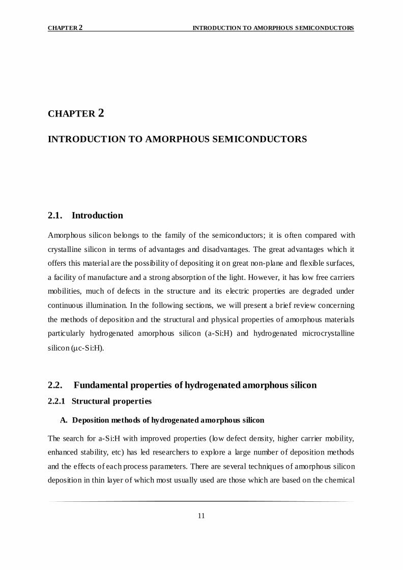
Figure 2.1 schematically describes the processes involved in a-Si:H deposition, which can be
decomposed into four steps: [2]
The dissociation of the gas precursors;
The plasma physics and chemistry, which determine the flux and nature of reactive
species to the substrate;
The plasma-surface interactions;
The reactions taking place in a growth-zone where cross-linking reactions result in the
formation of the film.
Figure 2.1: Schematic representation of the processes involved in a-Si:H deposition.
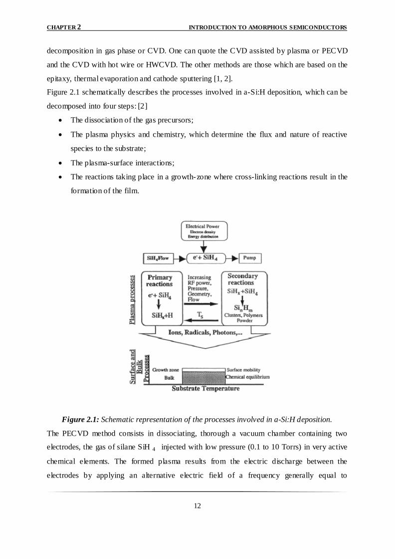
The PECVD method consists in dissociating, thorough a vacuum chamber containing two
electrodes, the gas of silane SiH 4 injected with low pressure (0.1 to 10 Torrs) in very active
chemical elements. The formed plasma results from the electric discharge between the
electrodes by applying an alternative electric field of a frequency generally equal to
CHAPTER 2 INTRODUCTION TO AMORPHOUS SEMICONDUCTORS
13
13.56MHz. It contains the radicals Si, Si-H, Si-H2; Si-H3 accompanied by the positive and
negative ionic species and the electrons what ensures total electric neutrality.
Turban [3] studied the chemical reactions and the mechanisms of dissociation of silane in
such plasma. The ionized molecules are deposited on the heated substrate (150-300°C) by
forming a thin film of hydrogenated amorphous silicon with a few Angströms per second
deposition rate. These depositions are generally carried out on glass substrates or glass
covered with a transparent and conducting layer (TCO).
Interestingly, with the growth of a-Si:H by PECVD dopants can be mixed with silane in a
controlled way to achieve the desired doping level. The most common dopants have been
used are phosphine and diborane; phosphine PH3 for a layer of N type and diborane B2H6 for a
layer of P type. The electric quality of the layers deposited depends in general on the
excitation frequency mode, the pressure and the flow of the gases, the level of vacuum, the
nature and the temperature of the substrate. [4]
PECVD decomposition of silane is schematically presented on figure 2.2.
Figure 2.2: System of deposition of hydrogenated amorphous silicon layers
CHAPTER 2 INTRODUCTION TO AMORPHOUS SEMICONDUCTORS
14
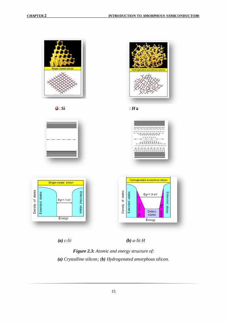
B. Atomic structure
Amorphous silicon (a-Si), unlike crystal silicon (c-Si), does not have a regular atomic
organization at long distance. In fact, a short range order persists i.e. the tetrahedral
configuration characteristic of the hybridization sp 3
where each atom is related to its four
neighbours by covalent bonds Si-Si is satisfied.
The distribution of the atoms of crystal silicon is periodic and regular in terms of
coordination, length and angles of the interatomic bonds (fig. 2.3.a). On the other hand, the
amorphous silicon shows a light variation on the level of the distance and angle of the bonds.
The magnitude of this disorder grows as one move away from the atom of reference. The
positions are distributed and a significant fraction of covalence bonds are broken, they
represent the dangling bonds. These latter form and act as recombination centres for the free
carriers and then determine the behaviour of material.
The amorphous silicon contains so much defects what makes it very difficult to be doped so
unusable for the optoelectronics applications. In a large majority of the cases the methods of
saturation of the dangling bonds by incorporating from 5 to 15% of hydrogen atoms in the
network during the deposition is favored in order to remove the large density of defect states
in the band gap and eliminate most of the trapping and recombination centers. In fact, by its
small size, it is possible to reduce the no satisfied bonds what improves considerably the
properties of the materials (fig. 2.3.b). Thus, the possibility of doping of the a-Si:H was
demonstrated by W.E.Spear [5].
Infra-red absorption shows that with slight hydrogen concentration (lower than 10%), the
radicals present are SiH and SiH2 while with high hydrogen concentration the radicals present
are (SiH2) n [6]. Let us note that the addition of hydrogen not only passivates dangling bonds
but preserves also the short-range order and increases the band gap width by the fact that the
binding energy Si-H (3.4eV) is higher than the weak bonds Si-Si (2.2eV) [7].
CHAPTER 2 INTRODUCTION TO AMORPHOUS SEMICONDUCTORS
15
: Si : H
(a) c-Si (b) a-Si:H
Figure 2.3: Atomic and energy structure of:
(a) Crystalline silicon; (b) Hydrogenated amorphous silicon.
CHAPTER 2 INTRODUCTION TO AMORPHOUS SEMICONDUCTORS
16
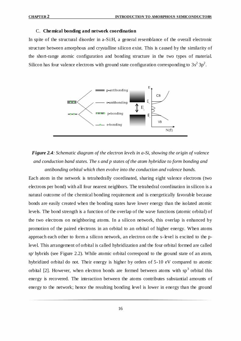
C. Chemical bonding and network coordination
In spite of the structural disorder in a-Si:H, a general resemblance of the overall electronic
structure between amorphous and crystalline silicon exist. This is caused by the similarity of
the short-range atomic configuration and bonding structure in the two types of material.
Silicon has four valence electrons with ground state configuration corresponding to 3s2 3p2.
Figure 2.4: Schematic diagram of the electron levels in a-Si, showing the origin of valence
and conduction band states. The s and p states of the atom hybridize to form bonding and
antibonding orbital which then evolve into the conduction and valence bands.
Each atom in the network is tetrahedrally coordinated, sharing eight valence electrons (two
electrons per bond) with all four nearest neighbors. The tetrahedral coordination in silicon is a
natural outcome of the chemical bonding requirement and is energetically favorable because
bonds are easily created when the bonding states have lower energy than the isolated atomic
levels. The bond strength is a function of the overlap of the wave functions (atomic orbital) of
the two electrons on neighboring atoms. In a silicon network, this overlap is enhanced by
promotion of the paired electrons in an orbital to an orbital of higher energy. When atoms
approach each other to form a silicon network, an electron on the s- level is excited to the p-
level. This arrangement of orbital is called hybridization and the four orbital formed are called
sp3 hybrids (see Figure 2.2). While atomic orbital correspond to the ground state of an atom,
hybridized orbital do not. Their energy is higher by orders of 5-10 eV compared to atomic
orbital [2]. However, when electron bonds are formed between atoms with sp3 orbital this
energy is recovered. The interaction between the atoms contributes substantial amounts of
energy to the network; hence the resulting bonding level is lower in energy than the ground
CHAPTER 2 INTRODUCTION TO AMORPHOUS SEMICONDUCTORS
17
atomic state. The increase in energy caused by the formation of these bonds is conventionally
known as cohesion energy. The atomic interaction within the structural network causes the
orbital to broaden into bands separated by the band gap of the material as shown in Figure 2.2.
It is meaningful to note that this explanation is not dependent on symmetry considerations and
therefore also applies to amorphous solids. While the anti-bonding states are empty, the
bonding states (valency) have the lowest energy and are usually occupied. Interposed on
Figure 2.2 is an illustration of the density of states as a function of energy for such a band
diagram. We note the existence of states at energy levels lying in the middle of the gap. These
states are the non-bonding states attributed to structural defects such as dangling bonds in
amorphous silicon. Obviously, the origin of the similarities in the overall electronic structure
of a-Si:H and c-Si reflect the chemistry of the silicon atom. It follows that the same chemical
interactions that control the structure of crystalline silicon are present in amorphous silicon.
However, a complete description of the roles of local chemistry in amorphous and crystalline
silicon requires specification of the network topology that defines the way in which atomic
sites are interconnected with each other. For covalent systems such as silico n, chemical
ordering is predicted by the so called “8-N rule” formulated by Mott [5], where N designates
the number of valence electrons. This means that, if for example elements X and Y are in
columns a and b of the periodic table, the coordination of X and Y atoms has an optimal
number of coordinations given by za = 8 - a and zb = 8 - b. The 8-N rule is only applicable to
elements belonging to columns IV-VII of the periodic table. The rule suggests that each atom
adopts a coordination which results in fully occupied bonding states and empty non-bonding
states [6]. With this analysis, it is easy to speculate about the origins of the electronically
induced structural reactions that are prevalent in amorphous silicon since any non-optimal
value of the coordination number z will result in a high energy configuration. For covalent
solids, it is found that the atom can form a defect center when z deviates from the 8-N rule
[7]. In crystalline silicon, the equilibrium position of each atom is when its coordinat ion
number, its bond lengths and its bond angles are optimized to achieve the lowest energy state.
Amorphous silicon is not the lowest energy structure of the silicon network; it has deviations
from the optimal atomic coordination which result into coordination defects (dangling bonds)
and deviations from optimal bond lengths or bond angles which result into strained bonds.
Both dangling bonds and strained bonds can yield localized states in the gap of a-Si as
described in the following sections of this chapter.
CHAPTER 2 INTRODUCTION TO AMORPHOUS SEMICONDUCTORS
18
2.2.2 Electronic structure
The general discussion of the above sections provide a very useful step in understanding the
electronic structure of a-Si:H. In the following section, we shall discuss the connection
between the atomic structure and the electronic properties of this material. It was shown that
the local bonding structure of the material is in a large part responsible for establishing the
significant features of amorphous to that of crystalline silicon. Thus the observed similarities
in the electronic structure of the two materials reside in a realization that many attractive
properties of amorphous silicon are controlled by the bonding chemistry as they are in
crystalline silicon. Nevertheless, the disorder which characterizes the structure of the
amorphous semiconductors such as irregular interatomic distances and angles and unsaturated
bonds by hydrogen, leads to an electronic energy structure different from that of the
crystalline semiconductors where the Bloch theorem is pertinent [8]. Consequently, the band
diagram is represented by an electronic distribution of states located in the forbidden band and
an asymmetry of the conduction and valence bands. One uses then the band gap mobility term
instead of forbidden band and edges of mobility instead of edges of bands.
a) Extended states
The energies of the electronic states are perturbed and the band broadens as a consequence of
the disorder represented by fluctuations in atomic configuration which causes in turn
fluctuations in the potential acting on an electron. In these circumstances, the sharp features
prevalent in crystalline density of states become smeared and form band tails which extend
into the forbidden gap. It is for this reason that, the sharply defined band edges of the valence
and conduction bands are non-existent in amorphous silicon.
b) Tail states or weak bonds
Calculations based on the tight-binding approach [8] have shown that the energies of anti-
bonding orbitals (s-like) and bonding orbitals (p- like) are differently affected by material
disorder. For example, the energies of the p states are more sensitive to the bonding disorder
than are the energies of the s-like states [8]. Consequently the shapes of the band tails in
amorphous silicon are not symmetrical, with fewer states in the conduction band tail than in
valence band tail. The existence of the tail states was predicted by the theory of Anderson [9],
and their presences in the gap of a-Si: H was established in experiments by various techniques
CHAPTER 2 INTRODUCTION TO AMORPHOUS SEMICONDUCTORS
19
such as the technique of photoemission or PES [5] and the technique of the time of flight or
TOF [10]. The valence band tail or VBT and conduction band tail or CBT are the direct result
of the weak bonds (irregular interatomic distances and abnormal angles of bonds). They are
localized states near to edges of mobility of which their density decrease exponentially
according to the following formula: [11]
,
,
,
expv c
v c
B v c
E ED E N
K T
(2.1)
Where Nv et Nc are density of states at Ev et Ec edges respectively;
Tv et Tc denote characteristic temperature for VBT and CBT respectively.
The states of VBT, known also under the name of Urbach tail (Urbach 1953) and determined
by the optical techniques [5], have typically a slope KBTv about 45-55meV. It is broader
opposite the slope KBTc of the states CBT which is typically about 20-30meV because the
states of VBT are more influenced by the disorder compared to the states of CBT. As a result
of the asymmetry in the distribution of localized states, the position of the Fermi level is
affected. As an example, in an undoped sample of amorphous s ilicon, the Fermi level in the
dark is generally shifted closer to the bottom of the conduction band. Hence, these states
determine several electrical properties of the material by controlling the process of multi-
trapping by their acceptors- like character close to the valence band or VB (they are neutral
when they are empty) and donors- like character close to the conduction band or CB (they are
neutral when they are filled).
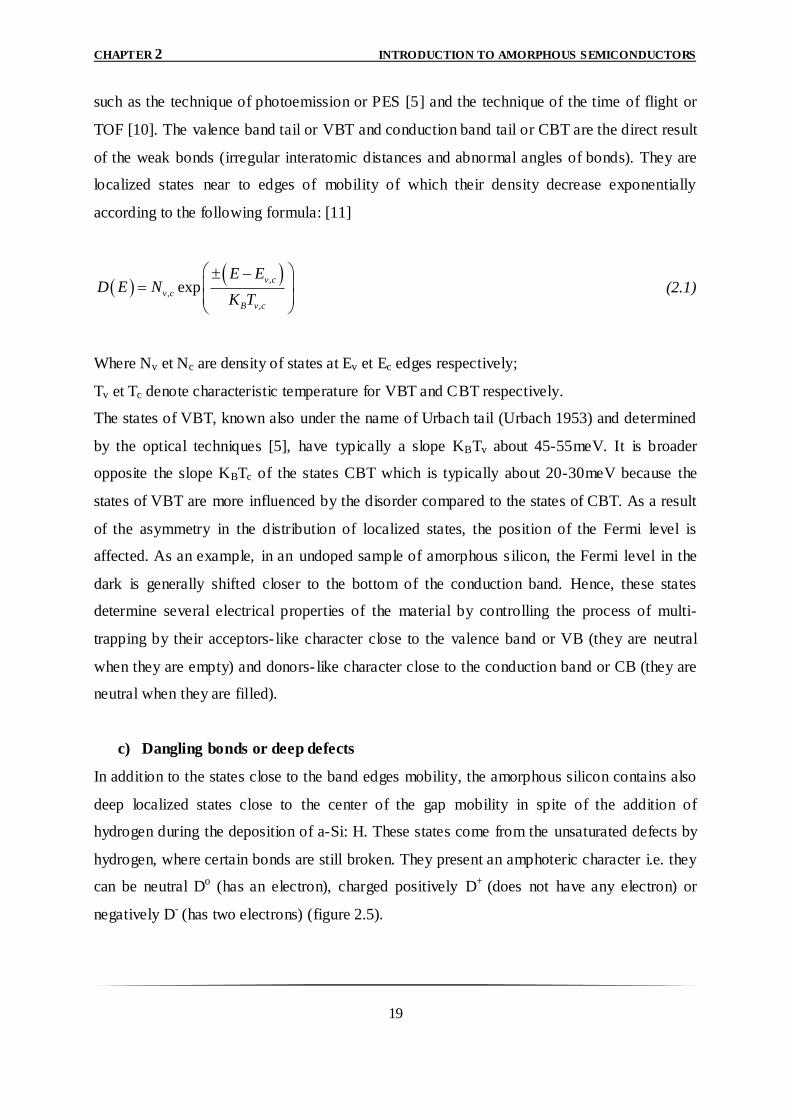
c) Dangling bonds or deep defects
In addition to the states close to the band edges mobility, the amorphous silicon contains also
deep localized states close to the center of the gap mobility in spite of the addition of
hydrogen during the deposition of a-Si: H. These states come from the unsaturated defects by
hydrogen, where certain bonds are still broken. They present an amphoteric character i.e. they
can be neutral Do (has an electron), charged positively D+ (does not have any electron) or
negatively D- (has two electrons) (figure 2.5).
CHAPTER 2 INTRODUCTION TO AMORPHOUS SEMICONDUCTORS
20
positive neutral negative
Figure 2.5: Dangling bonds charge states
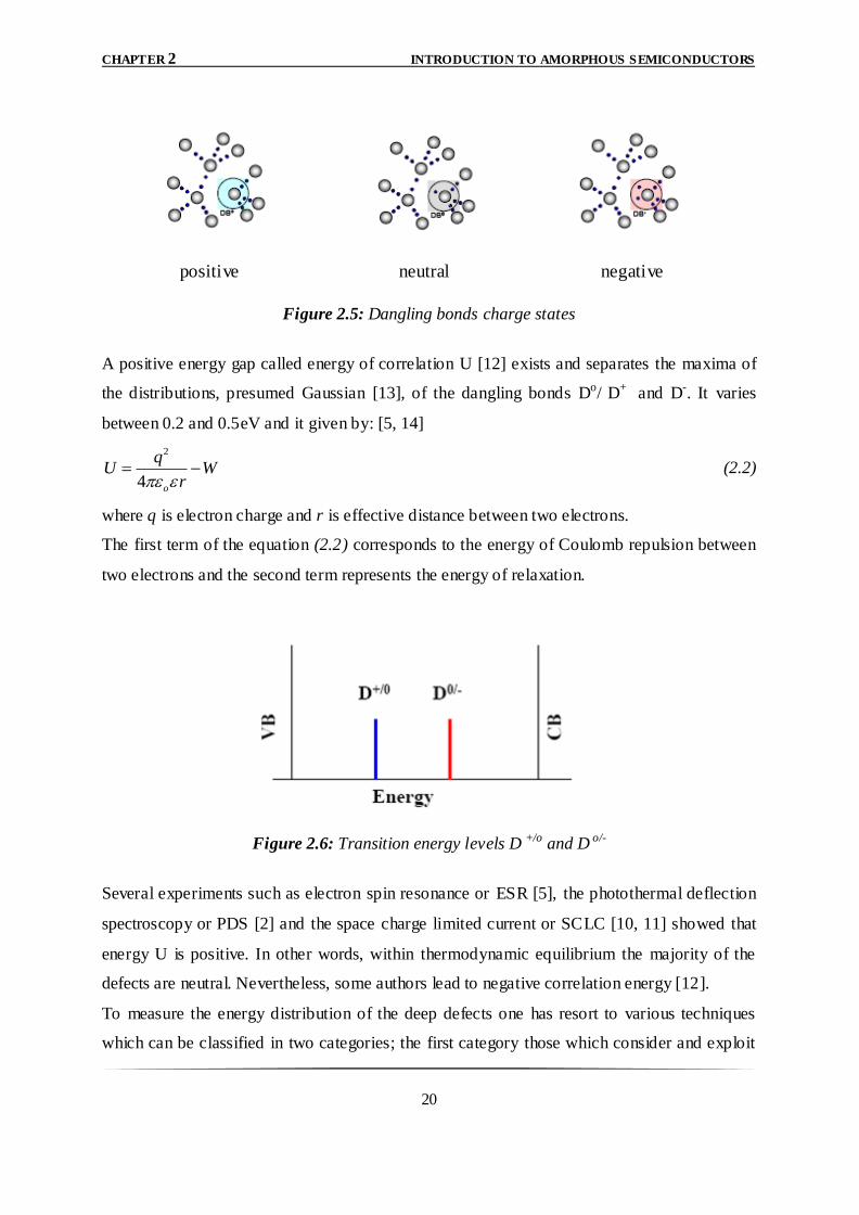
A positive energy gap called energy of correlation U [12] exists and separates the maxima of
the distributions, presumed Gaussian [13], of the dangling bonds Do/ D+ and D-. It varies
between 0.2 and 0.5eV and it given by: [5, 14]
2
4 o
qU W
r (2.2)
where q is electron charge and r is effective distance between two electrons.
The first term of the equation (2.2) corresponds to the energy of Coulomb repulsion between
two electrons and the second term represents the energy of relaxation.
Figure 2.6: Transition energy levels D +/o and D o/-
Several experiments such as electron spin resonance or ESR [5], the photothermal deflection
spectroscopy or PDS [2] and the space charge limited current or SCLC [10, 11] showed that
energy U is positive. In other words, within thermodynamic equilibrium the majority of the
defects are neutral. Nevertheless, some authors lead to negative correlation energy [12].
To measure the energy distribution of the deep defects one has resort to various techniques
which can be classified in two categories; the first category those which consider and exploit
CHAPTER 2 INTRODUCTION TO AMORPHOUS SEMICONDUCTORS
21
the thermal transitions like deep level transient spectroscopy or DLTS [11] and the second
category are those which consider and exploit the optical transitions such as PDS. Differences
were found concerning the nature, the distribution and the density of states of Do, D+ and D-.
The most used are the standard model and the defect pool model [15, 16]. The latter model is
adopted in our study.
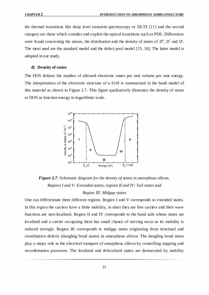
d) Density of states
The DOS defines the number of allowed electronic states per unit volume per unit energy.
The interpretation of the electronic structure of a-Si:H is summarized in the band model of
this material as shown in Figure 2.7. This figure qualitatively illustrates the density of states
or DOS as function energy in logarithmic scale.
Figure 2.7: Schematic diagram for the density of states in amorphous silicon.
Regions I and V: Extended states, regions II and IV: Tail states and
Region III: Midgap states
One can differentiate three different regions: Region I and V corresponds to extended states.
In this region the carriers have a finite mobility, in short they are free carriers and their wave
functions are non- localized. Region II and IV corresponds to the band tails whose states are
localized and a carrier occupying them has small chance of moving away as its mobility is
reduced strongly. Region III corresponds to midgap states originating from structural and
coordination defects (dangling bond states) in amorphous silicon. The dangling bond states
play a major role in the electrical transport of amorphous silicon by controlling trapping and
recombination processes. The localized and delocalized states are demarcated by mobility
CHAPTER 2 INTRODUCTION TO AMORPHOUS SEMICONDUCTORS
22
edges EC and EV as proposed by Mott and Davis (1979). The mobility gap Emob is defined as
the region between these two energies. The hypothesis advanced by Mott [9], asserts that at
zero absolute temperature (T=0), the extended states offer finite mobility of the carriers and
zero mobility for localized states. This statement suggests an abrupt transition of mobility at
the band edge energies EC and EV. However, the gradually decreasing densities of states from
extended to localized states suggest that localization of the electron wave function varies
smoothly as we move from extended states to states deep in the band gap. Obviously, the
shallowest states will generally have less localized electronic wave functions than the deepest
states near the center of the gap. This examination entails a smoothly increasing mobility from
localized to extended states. Unfortunately, the exact behavior of the properties of states near
the mobility edges is still not well known. There is no available quantitative technique for
characterizing these states [10].
2.2.3 Effects of doping
As soon as Spear and LeComber deferred in 1975 that a-Si: H can be doped by adding small
quantities of atoms of phosphorus or boron, the explanation and the exploitation of the effect
of doping on the properties of this material took a great importance.
As in crystalline silicon, if one introduces doping elements like boron or phosphorous in
amorphous structure, one hopes to achieve p-type or n-type doping. It appears that the doping
efficiency, which is defined as the fraction of introduced dopant atoms which indeed are
electrically active, is tremendously low in amorphous silicon. The reason that effective doping
in defect-rich material is not possible stems from the 8-N rule. The network topology of
amorphous silicon is such that various values of the coordination number z occur. In
crystalline silicon the value z can only be 4, but in amorphous silicon network values of 3 and
5 are also quite possible. Mott's rule states that normally a foreign element will prefer a site in
the network at which the coordination is such that a number of valence electrons n, together
with the number z of electrons from possible covalent bonds at this site, should add up to a
full shell, i.e 8, in order to minimize the energy at this position. In other words one can
conclude from this rule that elements like boron or phosphorus which are added to an
unhydrogenated amorphous silicon network will in general not show doping effects, since
they choose e.g a 3-fold coordination, in which no donor or acceptor states can be formed.
This interpretation of course generally applies only when the atoms indeed have possibilities
CHAPTER 2 INTRODUCTION TO AMORPHOUS SEMICONDUCTORS
23
to choose, i.e when they are mobile and also not yet fully built in. This is a situation which
occurs during deposition and growth of doped layer and can occur afterwards only at elevated
temperatures. The presence of hydrogen however serves to stabilize the network and, more
specifically, to greatly reduce the number of unpaired electrons or dangling bonds. In such a
network many dopant atoms therefore are forced in four- fold coordinated sites, in which they
will produce a doping effect in terms of donor or acceptor states. It may be understood that
the doping efficiency will be low, as compared to crystalline silicon. In the crystalline silicon
the efficiency of doping is of the order of unity, while in hydrogenated amorphous silicon it
can range from 10-4 to 10-2, depending on the deposition temperature. The details of the
doping process in amorphous silicon are more complicated than what has been described
above. It appears that there exists an intimate relation between the number of electrically
active dopants and the number of defects in the material. The doped materials are richer with
defects than undoped hydrogenated amorphous silicon.
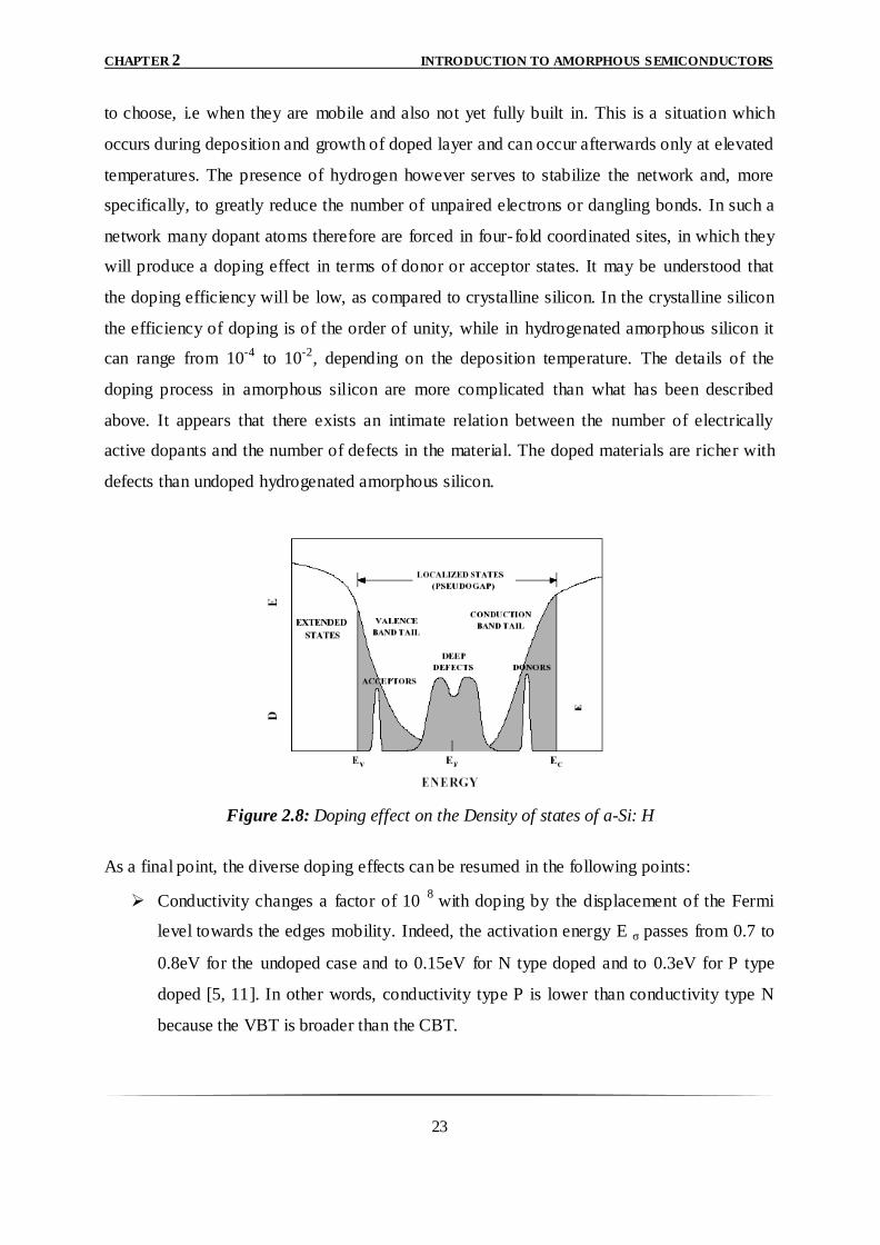
Figure 2.8: Doping effect on the Density of states of a-Si: H
As a final point, the diverse doping effects can be resumed in the following points:
Conductivity changes a factor of 10 8
with doping by the displacement of the Fermi
level towards the edges mobility. Indeed, the activation energy E σ passes from 0.7 to
0.8eV for the undoped case and to 0.15eV for N type doped and to 0.3eV for P type
doped [5, 11]. In other words, conductivity type P is lower than conductivity type N
because the VBT is broader than the CBT.
CHAPTER 2 INTRODUCTION TO AMORPHOUS SEMICONDUCTORS
24
The doping introduced into the crystalline semiconductors donors or acceptors
electronic levels close to the conduction or the valence band. Regarding to the
amorphous semiconductors, in addition to these shallow states (see fig. 2.8), doping
increases the density of the defects ND following the empirical relation: [2,5]
19 33.10D RN c cm (2.3)
with cR is the doping density factor.
Doping reduces also the gap width and increases the slope of the CBT and VBT what
involves the reduction in the mobility of electrons and the holes [17].
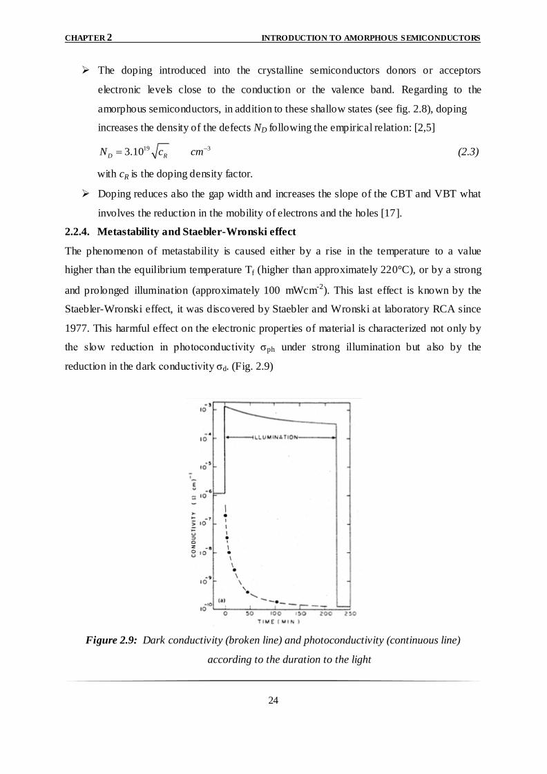
2.2.4. Metastability and Staebler-Wronski effect
The phenomenon of metastability is caused either by a rise in the temperature to a value
higher than the equilibrium temperature Tf (higher than approximately 220°C), or by a strong
and prolonged illumination (approximately 100 mWcm-2). This last effect is known by the
Staebler-Wronski effect, it was discovered by Staebler and Wronski at laboratory RCA since
1977. This harmful effect on the electronic properties of material is characterized not only by
the slow reduction in photoconductivity σph under strong illumination but also by the
reduction in the dark conductivity σd. (Fig. 2.9)
Figure 2.9: Dark conductivity (broken line) and photoconductivity (continuous line)
according to the duration to the light
CHAPTER 2 INTRODUCTION TO AMORPHOUS SEMICONDUCTORS
25
The initial properties of material can be recovered by an annealing of a few hours at a
temperature of 150°C (423K), it is a phenomenon known as reversible.
In spite of the intense attempts for the comprehension of this effect in a-Si: H, it still needs
more explanations. One can recapitulate the critical points related to this effect in the
following way:
The dominant metastable defects are the dangling bonds. Their densities pass from
1016cm-3 in an initial state to 1017cm-3 in a degraded state of the material [7];
Photoconductivity can decrease by a factor of 10 [18];
The effect only appears in intrinsic films, while in strongly doped films the effect does
not appear [19];
The majority of the theories include S-W effect in volume. Though, the probability of
the creation of the metastable defects on the surface remains possible [6];
Several microscopic models were proposed to explain the mechanism of creation of
defects under the strong and prolonged illumination; one of them is based on the break
of the weakest bonds silicon-silicon (Si-Si) where hydrogen plays a significant role
[20,21];
The shift of the Fermi level toward the middle of the gap of mobility under the
illumination involves the reduction in σd. This is due to the increasing of DB density;
The rose factor γ which connects the photoconductivity to the intensity of the optical
excitation ( ph G ), pass from 0.5 before to 0.9 after the illumination [7];
Fortunately, the S-W effect is reversible and there is a saturation point of the
degradation which depends on the conditions of deposition [4, 18].
2.2.5. Optical properties of the a-Si:H
a) Optical gap
We have earlier mentioned that the structure of a-Si:H can be described as a continuous
random network, but in a real a-Si:H network the short range order may differ from one site to
another. The slight distortions in the atomic configuration results into random distribution of
charged centers leading to a non-periodic potential. A disordered potential can lead to strong
electronic scattering and a short coherence length of the electron wave function. In amorphous
silicon the coherence length is approximately of the order of the lattice spacing and the
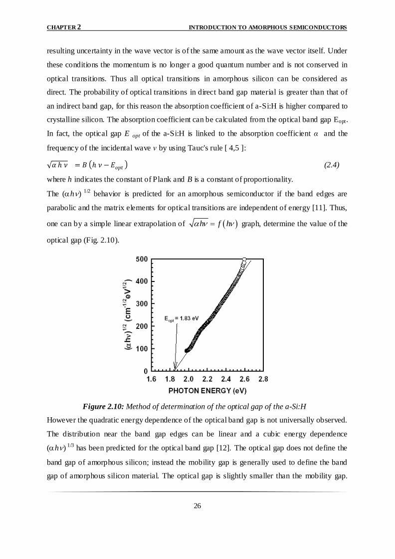
CHAPTER 2 INTRODUCTION TO AMORPHOUS SEMICONDUCTORS
26
resulting uncertainty in the wave vector is of the same amount as the wave vector itself. Under
these conditions the momentum is no longer a good quantum number and is not conserved in
optical transitions. Thus all optical transitions in amorphous silicon can be considered as
direct. The probability of optical transitions in direct band gap material is greater than that of
an indirect band gap, for this reason the absorption coefficient of a-Si:H is higher compared to
crystalline silicon. The absorption coefficient can be calculated from the optical band gap Eopt.
In fact, the optical gap E opt of the a-Si:H is linked to the absorption coefficient α and the
frequency of the incidental wave ν by using Tauc's rule [ 4,5 ]:
𝛼 ℎ 𝜈 = 𝐵 ℎ 𝜈 −𝐸𝑜𝑝𝑡 (2.4)
where h indicates the constant of Plank and B is a constant of proportionality.
The (h) 1/2 behavior is predicted for an amorphous semiconductor if the band edges are
parabolic and the matrix elements for optical transitions are independent of energy [11]. Thus,
one can by a simple linear extrapolation of h f h graph, determine the value of the
optical gap (Fig. 2.10).
Figure 2.10: Method of determination of the optical gap of the a-Si:H
However the quadratic energy dependence of the optical band gap is not universally observed.
The distribution near the band gap edges can be linear and a cubic energy dependence
(h) 1/3 has been predicted for the optical band gap [12]. The optical gap does not define the
band gap of amorphous silicon; instead the mobility gap is generally used to define the band
gap of amorphous silicon material. The optical gap is slightly smaller than the mobility gap.
CHAPTER 2 INTRODUCTION TO AMORPHOUS SEMICONDUCTORS
27
Since the energy of the mobility edge depends strongly on the extent of material disorder, the
band gap of amorphous silicon can be varied according to the degree of disorder. The optical
gap depends, independently of the method of deposition of film, the hydrogen concentration
and doping [4]. The optical gap can be used to estimate the energy of photons that can be
absorbed by a-Si:H. By decreasing the optical gap, one can increase the part of the solar
spectrum that is absorbed by a-Si:H.
b) Optical absorption
The optical absorption properties of amorphous silicon are very important for understanding
the operation of a solar cell and for optimizing its conversion efficiency. Thus the weight of
understanding the absorption processes in a-Si:H stems from their use as a probe for the local
structure of a-Si:H network. From absorption measurements, one can deduce information on
both the tail and defect states.
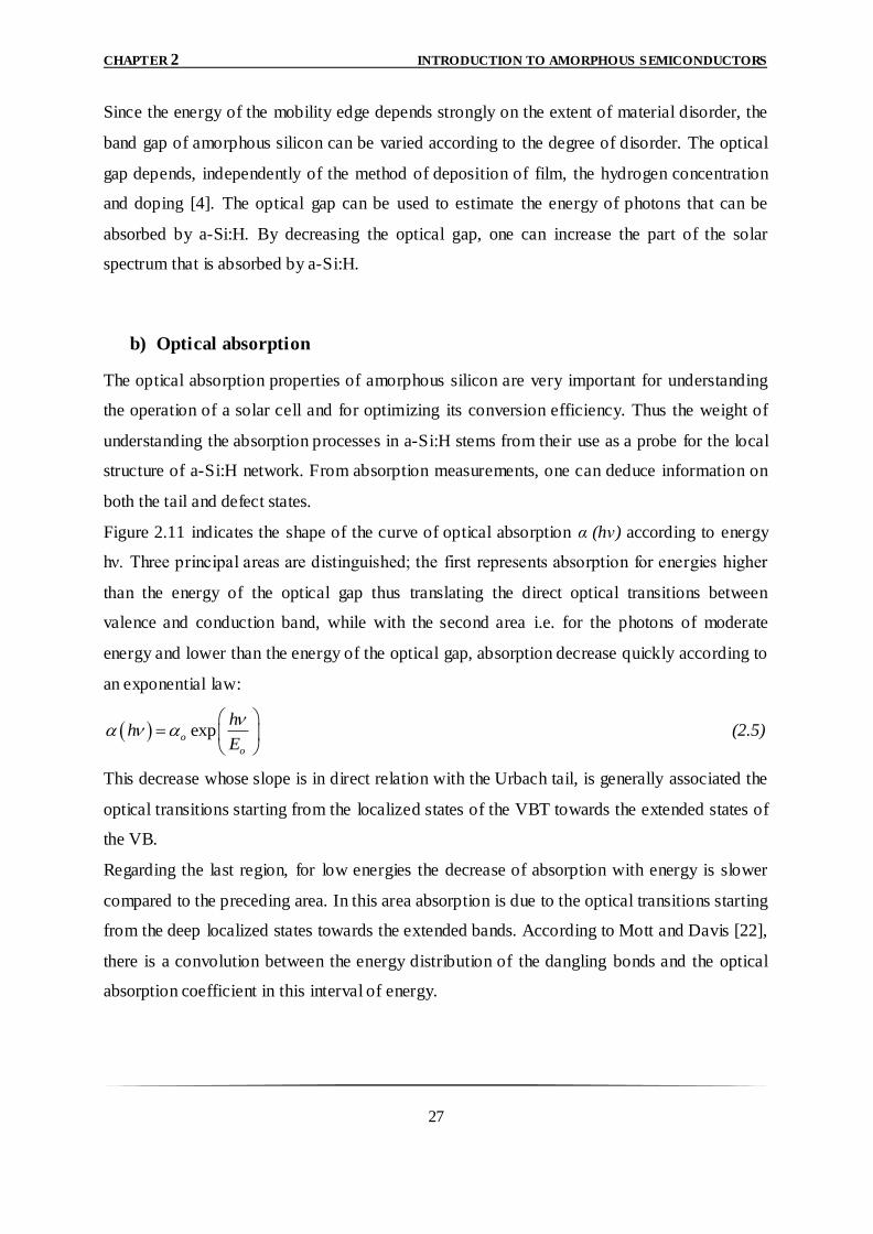
Figure 2.11 indicates the shape of the curve of optical absorption α (hν) according to energy
hν. Three principal areas are distinguished; the first represents absorption for energies higher
than the energy of the optical gap thus translating the direct optical transitions between
valence and conduction band, while with the second area i.e. for the photons of moderate
energy and lower than the energy of the optical gap, absorption decrease quickly according to
an exponential law:
expo
o
hh
E
(2.5)
This decrease whose slope is in direct relation with the Urbach tail, is generally associated the
optical transitions starting from the localized states of the VBT towards the extended states of
the VB.
Regarding the last region, for low energies the decrease of absorption with energy is slower
compared to the preceding area. In this area absorption is due to the optical transitions starting
from the deep localized states towards the extended bands. According to Mott and Davis [22],
there is a convolution between the energy distribution of the dangling bonds and the optical
absorption coefficient in this interval of energy.
CHAPTER 2 INTRODUCTION TO AMORPHOUS SEMICONDUCTORS
28
Figure 2.11: Optical absorption spectrum of the a-Si:H and corresponding optical transitions
Let us note that the dependent hydrogen concentration and the nature of the bonds can be
extracted by measuring α (hν) [23, 24]. One sees immediately that accurate measurement of
absorption spectrum for various temperatures and illuminations, allows us to know various
properties of material studied in an initial or degraded state for instance the mechanisms of
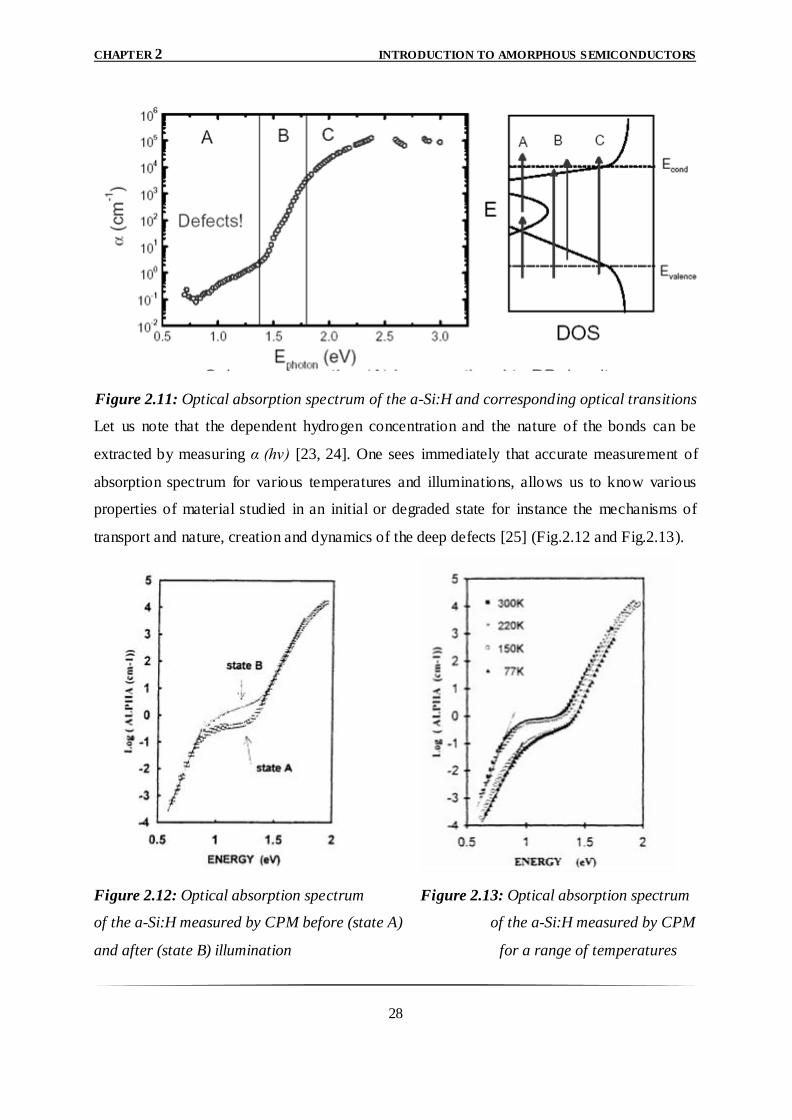
transport and nature, creation and dynamics of the deep defects [25] (Fig.2.12 and Fig.2.13).
Figure 2.12: Optical absorption spectrum Figure 2.13: Optical absorption spectrum
of the a-Si:H measured by CPM before (state A) of the a-Si:H measured by CPM
and after (state B) illumination for a range of temperatures
CHAPTER 2 INTRODUCTION TO AMORPHOUS SEMICONDUCTORS
29
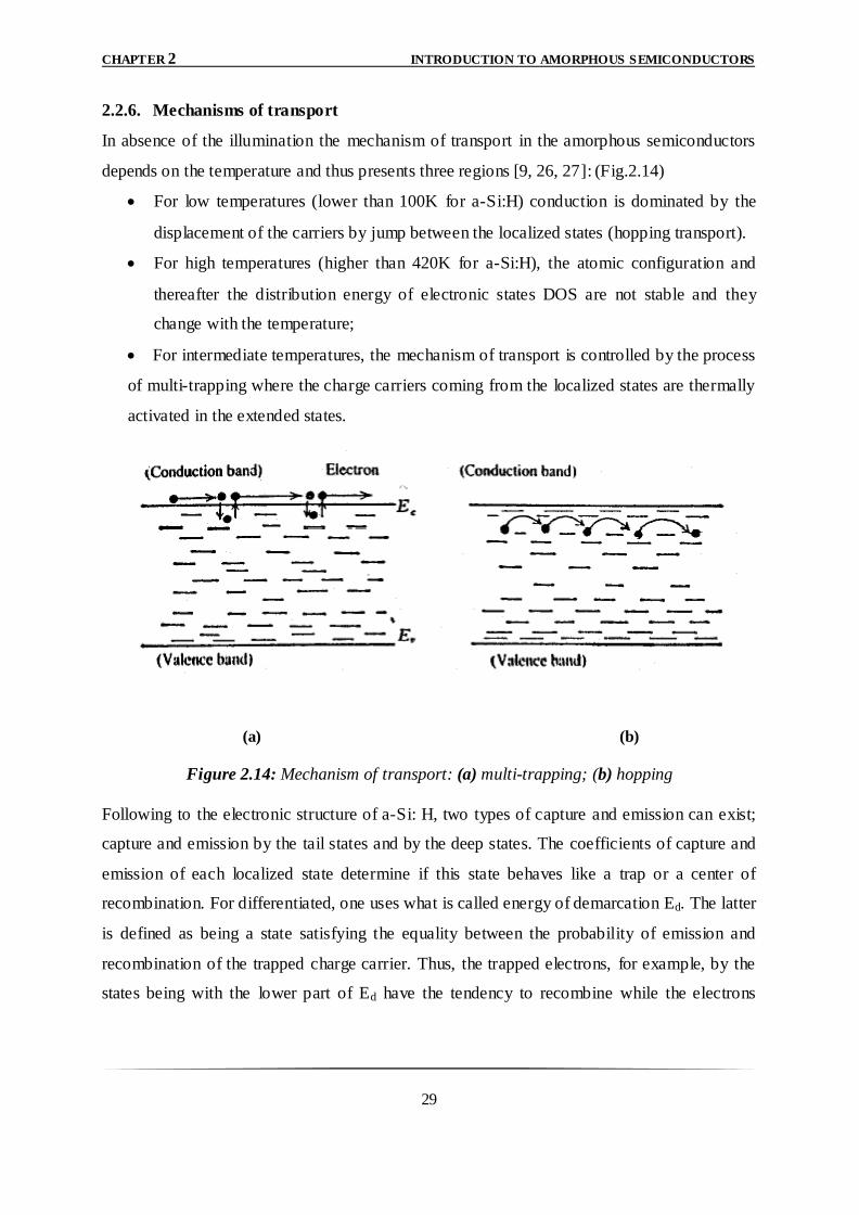
2.2.6. Mechanisms of transport
In absence of the illumination the mechanism of transport in the amorphous semiconductors
depends on the temperature and thus presents three regions [9, 26, 27]: (Fig.2.14)
For low temperatures (lower than 100K for a-Si:H) conduction is dominated by the
displacement of the carriers by jump between the localized states (hopping transport).
For high temperatures (higher than 420K for a-Si:H), the atomic configuration and
thereafter the distribution energy of electronic states DOS are not stable and they
change with the temperature;
For intermediate temperatures, the mechanism of transport is controlled by the process
of multi-trapping where the charge carriers coming from the localized states are thermally
activated in the extended states.
Figure 2.14: Mechanism of transport: (a) multi-trapping; (b) hopping
Following to the electronic structure of a-Si: H, two types of capture and emission can exist;
capture and emission by the tail states and by the deep states. The coefficients of capture and
emission of each localized state determine if this state behaves like a trap or a center of
recombination. For differentiated, one uses what is called energy of demarcation Ed. The latter
is defined as being a state satisfying the equality between the probability of emission and
recombination of the trapped charge carrier. Thus, the trapped electrons, for example, by the
states being with the lower part of Ed have the tendency to recombine while the electrons
(a) (b)
CHAPTER 2 INTRODUCTION TO AMORPHOUS SEMICONDUCTORS
30
trapped in the states being located at the top of Ed have the tendency to be emitted towards the
conduction band.
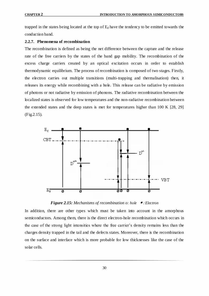
2.2.7. Phenomena of recombination
The recombination is defined as being the net difference between the capture and the release
rate of the free carriers by the states of the band gap mobility. The recombination of the
excess charge carriers created by an optical excitation occurs in order to establish
thermodynamic equilibrium. The process of recombination is composed of two stages. Firstly,
the electron carries out multiple transitions (multi- trapping and thermalisation) then, it
releases its energy while recombining with a hole. This release can be radiative by emission
of photons or not radiative by emission of phonons. The radiative recombination between the
localized states is observed for low temperatures and the non-radiative recombination between
the extended states and the deep states is met for temperatures higher than 100 K [28, 29]
(Fig.2.15).
Figure 2.15: Mechanisms of recombination o: hole • : Electron
In addition, there are other types which must be taken into account in the amorphous
semiconductors. Among them, there is the direct electron-hole recombination which occurs in
the case of the strong light intensities where the free carrier‟s density remains less than the
charges density trapped in the tail and the defects states. Moreover, there is the recombination
on the surface and interface which is more probable for low thicknesses like the case of the
solar cells.
CHAPTER 2 INTRODUCTION TO AMORPHOUS SEMICONDUCTORS
31
The recombination centres are mainly the dangling bonds for the a-Si:H, because these bonds
are close to the medium of the gap where the probability that a charge carrier recombined is
higher than the probability of being emitted.
2.3. Fundamental properties of hydrogenated micro crystalline silicon
μc-Si:H
2.3.1. Deposition methods of hydrogenated micro crystalline silicon
Usually, to obtain microcrystalline deposition, additional hydrogen source gas is added during
the deposition. Fortunately, a diversity of methods is used for the deposition of μc-Si:H.
Microcrystalline silicon grown by PECVD, is a promising material for the application as an
intrinsic absorber layer in solar cells: Best efficiencies have been obtained using this
technique. For the deposition of high-quality material at high deposition rates, conditions of
source gas depletion at high pressure (HPD: high-pressure depletion), PECVD regimes
featuring higher RF frequencies (VHF: very high frequency), and altered electrode designs are
explored. Alternative techniques exist to deposit μc-Si:H at high growth rate such as hot-wire
chemical vapor deposition (HWCVD), micro-wave plasma-enhanced chemical vapor
deposition (MW-PECVD) and expanding thermal plasma (EPT).
2.3.2. Atomic structure
Microcrystalline silicon is a mixed phase material consisting of c-Si, a-Si:H, nano-crystallites,
and grain boundaries. During the layer growth, crystallite formation starts with nucleation
after an amorphous incubation phase. In the continuing layer deposition, clusters of
crystallites grow (crystallization phase) till a saturated crystalline fraction is reached.
These processes are greatly dependent on the deposition condition. Generally, it can be stated
that these processes are enhanced by the presence of atomic hydrogen due to the chemical
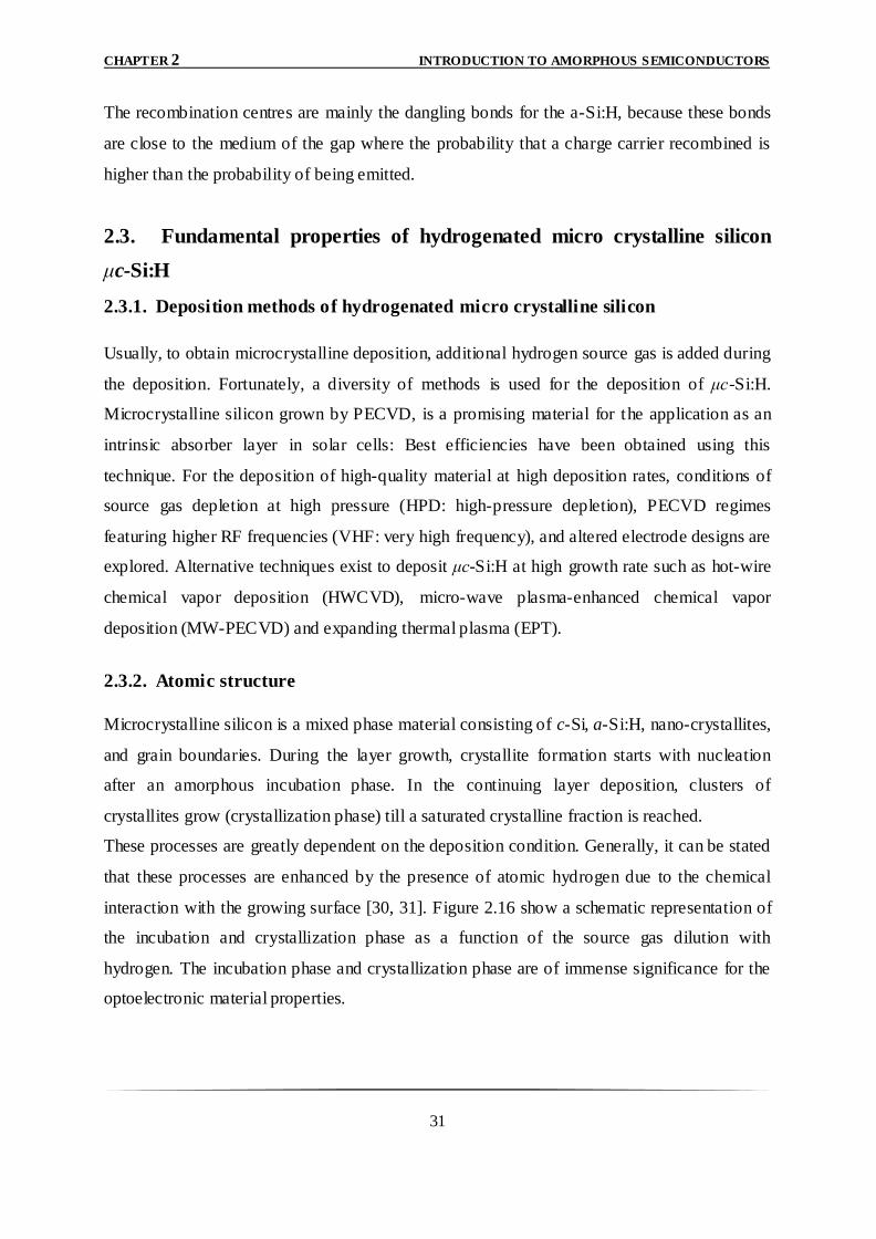
interaction with the growing surface [30, 31]. Figure 2.16 show a schematic representation of
the incubation and crystallization phase as a function of the source gas dilution with
hydrogen. The incubation phase and crystallization phase are of immense significance for the
optoelectronic material properties.
CHAPTER 2 INTRODUCTION TO AMORPHOUS SEMICONDUCTORS
32
Figure 2.16: Schematic representation of structure features found in μc-Si:H. From left to right the
film composition changes from highly crystalline to amorphous according to reference [31]
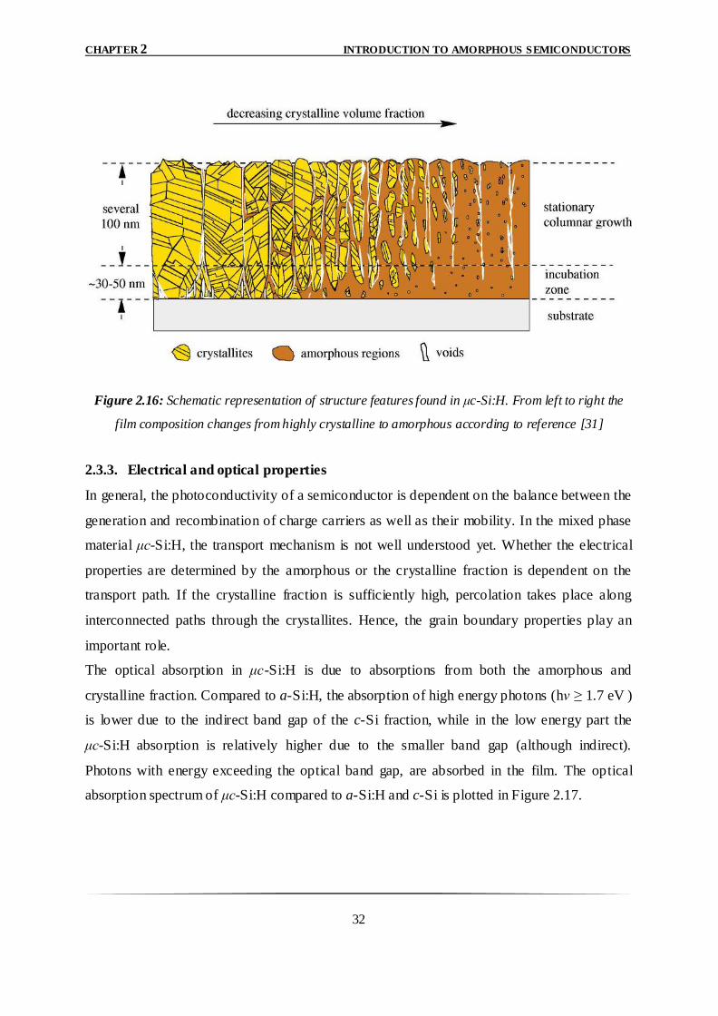
2.3.3. Electrical and optical properties
In general, the photoconductivity of a semiconductor is dependent on the balance between the
generation and recombination of charge carriers as well as their mobility. In the mixed phase
material μc-Si:H, the transport mechanism is not well understood yet. Whether the electrical
properties are determined by the amorphous or the crystalline fraction is dependent on the
transport path. If the crystalline fraction is sufficiently high, percolation takes place along
interconnected paths through the crystallites. Hence, the grain boundary properties play an
important role.
The optical absorption in μc-Si:H is due to absorptions from both the amorphous and
crystalline fraction. Compared to a-Si:H, the absorption of high energy photons (hν ≥ 1.7 eV )
is lower due to the indirect band gap of the c-Si fraction, while in the low energy part the
μc-Si:H absorption is relatively higher due to the smaller band gap (although indirect).
Photons with energy exceeding the optical band gap, are absorbed in the film. The optical
absorption spectrum of μc-Si:H compared to a-Si:H and c-Si is plotted in Figure 2.17.
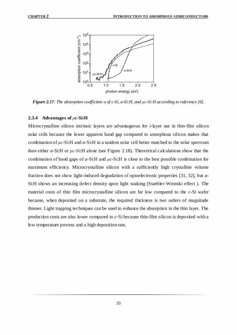
CHAPTER 2 INTRODUCTION TO AMORPHOUS SEMICONDUCTORS
33
Figure 2.17: The absorption coefficient α of c-Si, a-Si:H, and μc-Si:H according to reference [6].
2.3.4 Advantages of μc-Si:H
Microcrystalline silicon intrinsic layers are advantageous for i-layer use in thin-film silicon
solar cells because the lower apparent band gap compared to amorphous silicon makes that
combination of μc-Si:H and a-Si:H in a tandem solar cell better matched to the solar spectrum
than either a-Si:H or μc-Si:H alone (see Figure 2.18). Theoretical calculations show that the
combination of band gaps of a-Si:H and μc-Si:H is close to the best possible combination for
maximum efficiency. Microcrystalline silicon with a sufficiently high crystalline volume
fraction does not show light- induced degradation of optoelectronic properties [31, 32], but a-
Si:H shows an increasing defect density upon light soaking (Staebler-Wronski effect ). The
material costs of thin film microcrystalline silicon are far low compared to the c-Si wafer
because, when deposited on a substrate, the required thickness is two orders of magnitude
thinner. Light trapping techniques can be used to enhance the absorption in the thin layer. The
production costs are also lower compared to c-Si because thin-film silicon is deposited with a
low temperature process and a high deposition rate.
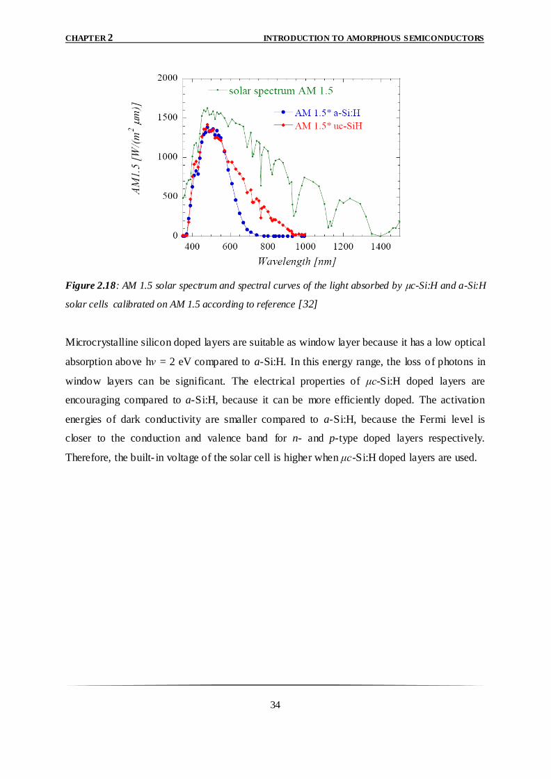
CHAPTER 2 INTRODUCTION TO AMORPHOUS SEMICONDUCTORS
34
Figure 2.18: AM 1.5 solar spectrum and spectral curves of the light absorbed by μc-Si:H and a-Si:H
solar cells calibrated on AM 1.5 according to reference [32]
Microcrystalline silicon doped layers are suitable as window layer because it has a low optical
absorption above hν = 2 eV compared to a-Si:H. In this energy range, the loss of photons in
window layers can be significant. The electrical properties of μc-Si:H doped layers are
encouraging compared to a-Si:H, because it can be more efficiently doped. The activation
energies of dark conductivity are smaller compared to a-Si:H, because the Fermi level is
closer to the conduction and valence band for n- and p-type doped layers respectively.
Therefore, the built- in voltage of the solar cell is higher when μc-Si:H doped layers are used.
CHAPTER 2 INTRODUCTION TO AMORPHOUS SEMICONDUCTORS
35
References
[1] Peter Munster, “Silicium intrinsèque et dopé in situ déposé amorphe par SAPCVD puis cristallisé en phase solide”, Thèse d‟état, Université de Rennes 1, France, 17 Juillet 2001.
[2] T. Searle, “Properties of Amorphous Silicon and its Alloys”, Edited by University of Sheffield, UK, 1998.
[3] G. Turbin, “Dissociation et transport dans un plasma de silane durant la croissance de
couches minces de silicium amorphe hydrogéné”, Thèse d‟état, Université de Nantes, France, 1981.
[4] Alain Ricaud, “Photopiles solaires, de la physique de la conversion photovoltaïque aux filières matériaux et procédés ”, Presses polytechniques et universitaires romandes, 1997.
[5] R. A. Street, “Hydrogenated amorphous silicon”, Cambridge university press, 1991.
[6] Zdenek Remes, Ph.D. thesis, “Study of defects and microstructure of amorphous and microcrystalline silicon thin films and polycrystalline diamond using optical methods”,
faculty of mathematics and physics, Charles university, Prague, Czech Republic, 1999.
[7] K. Takahashi & M. Konagai, “Amorphous silicon solar cells”, North Oxford academic publishers Ltd., 1986.
[8] C. Kittel, “Physique de l‟état solide”, Edition Dunod, Paris, France, 1998.
[9] M. F. Thorpe and L. Tichy, “Properties and Applications of Amorphous Materials”,
Proceedings of NATO Advanced Study Institute, Czech Republic, 25 June-7 July 2000.
[10] G. Seynhaeve, “Time-Of-Flight Photocurrents in Hydrogenated Amorphous Silicon”, Ph.D.thesis, Leuven, 1989.
[11] A. Treatise, “Semiconductors and Semimetals”, Volume 21, Part C, Academic Press Inc., Orlando, Florida, USA, 1984.
[12] N.Orita, T. Matsumura, H. Katayama-Yoshida, Journal of Non-Crystalline Solids 198- 200 (1996) 347-350.
[13] C.-Y. Lu, N. C.-C. Lu, C.-S. Wang, Solid-State Electronics 27 (1984), No. 5, p. 463-466.
[14] J.H. Zollondz, “Electronic Characterisation and Computer Modelling of Thin Film Materials and Devices for Optoelectronic Applications”, Ph.D.thesis, University of
Abertay, Dundee, UK, 2001.
[15] H.Dücker, O. Hein, S. Knief, W. von Niessen, Th. Koslowski, Journal of Electron Spectroscopy and Related Phenomena 100 (1999) 105-118.
[16] J. Schmal, Journal of Non-Crystalline Solids 198-200 (1996) 387-390.
CHAPTER 2 INTRODUCTION TO AMORPHOUS SEMICONDUCTORS
36
[17] K. Pierz, B. Hilgenberg, H. Mell and G. Weiser, Journal of Non-Crystalline Solids 97&
98 (1987) 63-66.
[18] Christian Hof, “Thin film solar cells of amorphous silicon: influence of i- layer material
on cell efficiency”, UFO atelier fur Gestaltung & Verlag, Band 279, ISBN 3-930803-78-X, 1999.
[19] V. Nadazdy, R. Durny, I. Thurzo, E. Pinicik, Journal of Non-Crystalline Solids 277- 230
(1998) 316-319.
[20] M. Stutzmann, W. B. Jackson and C. C. Tsai, Physical Review B, Vol. 32, No.1, pp. 23-
47, July 1985.
[21] R. A. Street, Physica B 170(1991) 69-81.
[22] N. F. Mott and E. A. Davis, Electronic Processes in Non-Crystalline Materials,
Clarendon Press, U.K., 1979.
[23] M. Yamanaka, I. Sakata and T. Sekigawa, Jpn. J. Appl. Phys., Vol. 39 (2000), pp. 3302-
3307, Part 1, No. 6A, June 2000.
[24] I. Sakata, M. Yamanaka, T. Sekigawa and Y. Hayashi, Solid State Phenomena, Vols. 44-46,(1995) pp. 127-134.
[25] P. Slảdek and M. L. Thèye, L. Chahed, Journal of Non-Crystalline Solids 164-166 (1993) 363-366.
[26] A. Merazga, “Steady state and transient photoconductivity in n-type a-Si”, Ph.D.thesis, Dundee Institute of Technology, Dundee, UK, 1990.
[27] H. Overhof, Journal of Non-Crystalline Solids 227-230 (1998) 15-22.
[28] T. Pisarkiewicz, T. Stapinski, P. Wojcik, 43rd International Scientific Colloquium, Technical University of Ilmenau, September21-24,1998.
[29] F. Vaillant, D. Jousse, and J.-C. Bruyere, Philosophical Magazine B, Vol. 57, No.5, 649-661, 1988.
[30] Vetterl, O. Finger, F. Carius, R. Hapke, P. Houben, L. Kluth, O. Lambertz, A. Muck, A.
Rech, and B. Wagner, 2000, Solar Energy Materials and Solar Cells 62 97.
[31] Von Thorsten Dylla, “Electron Spin Resonance and Transient Photocurrent
Measurements on Microcrystalline Silicon”, PhD. thesis, Fachbereich Physik, Freie Universität Berlin, Germany, 2004.
[32] Urs Samuel Graf, “Single-chamber process development of microcrystalline Silicon solar
cells and high-rate deposited intrinsic layers”, PhD. thesis, Université de Neuchâtel, October 2005.
CHAPTER 3 CHARACTERISATION TECHNIQUES OF AMORPHOUS SEMICONDUCTORS
37
CHAPTER 3
CHARACTERISATION TECHNIQUES OF AMORPHOUS
SEMICONDUCTORS
3.1. Introduction
The totality of optoelectronic properties of a-Si:H films are related directly to the density of
electronic states D(E) in a-Si:H. In order to enhance the performance of a-Si:H based devices
such as solar cells, photodetectors and thin-film transistor where undoped a-Si:H layers play
the most important role, a low D(E) in undoped a-Si:H is essential. Measurement of the D (E)
and understanding of the nature of gap states are, therefore, very imperat ive. The development
of various techniques is so very significant and justified and the problem has received
considerable interest to conclude the D (E). These comprise both electrical and optical
methods.
Transient capacitance methods like deep- level transient spectroscopy (DLTS) [1,2] and
isothermal capacitance transient spectroscopy (ICTS) [1], which usually make use of a
Schottky barrier junction, are tested techniques for determining the D(E) below the Fermi
level. However, these methods are limited in their application to doped samples of low
resistivity. For high resistivity materials, such as undoped or compensated a-Si:H films, the
dielectric relaxation times are too long for the measurement of the capacitance which can
reflect the depletion width in the junction. SCLC-TOF [3] measurements do give quantitative
estimation of the D (E), but only above the Fermi level. However, the determination of the
D (E) below the Fermi level for undoped films is important, because gap states located below
the Fermi level include singly-occupied Si dangling bonds which are considered to be main
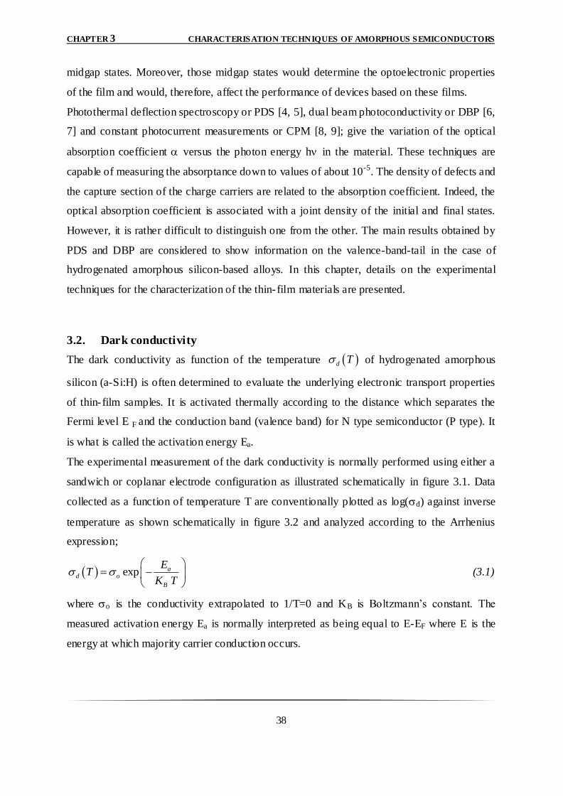
CHAPTER 3 CHARACTERISATION TECHNIQUES OF AMORPHOUS SEMICONDUCTORS
38
midgap states. Moreover, those midgap states would determine the optoelectronic properties
of the film and would, therefore, affect the performance of devices based on these films.
Photothermal deflection spectroscopy or PDS [4, 5], dual beam photoconductivity or DBP [6,
7] and constant photocurrent measurements or CPM [8, 9]; give the variation of the optical
absorption coefficient versus the photon energy h in the material. These techniques are
capable of measuring the absorptance down to values of about 10-5. The density of defects and
the capture section of the charge carriers are related to the absorption coefficient. Indeed, the
optical absorption coefficient is associated with a joint density of the initial and final states.
However, it is rather difficult to distinguish one from the other. The main results obtained by
PDS and DBP are considered to show information on the valence-band-tail in the case of
hydrogenated amorphous silicon-based alloys. In this chapter, details on the experimental
techniques for the characterization of the thin- film materials are presented.
3.2. Dark conductivity
The dark conductivity as function of the temperature d T of hydrogenated amorphous
silicon (a-Si:H) is often determined to evaluate the underlying electronic transport properties
of thin-film samples. It is activated thermally according to the distance which separates the
Fermi level E F and the conduction band (valence band) for N type semiconductor (P type). It
is what is called the activation energy Ea.
The experimental measurement of the dark conductivity is normally performed using either a
sandwich or coplanar electrode configuration as illustrated schematically in figure 3.1. Data
collected as a function of temperature T are conventionally plotted as log(d) against inverse
temperature as shown schematically in figure 3.2 and analyzed according to the Arrhenius
expression;
exp ad o
B
ET
K T
(3.1)
where o is the conductivity extrapolated to 1/T=0 and KB is Boltzmann‟s constant. The
measured activation energy Ea is normally interpreted as being equal to E-EF where E is the
energy at which majority carrier conduction occurs.
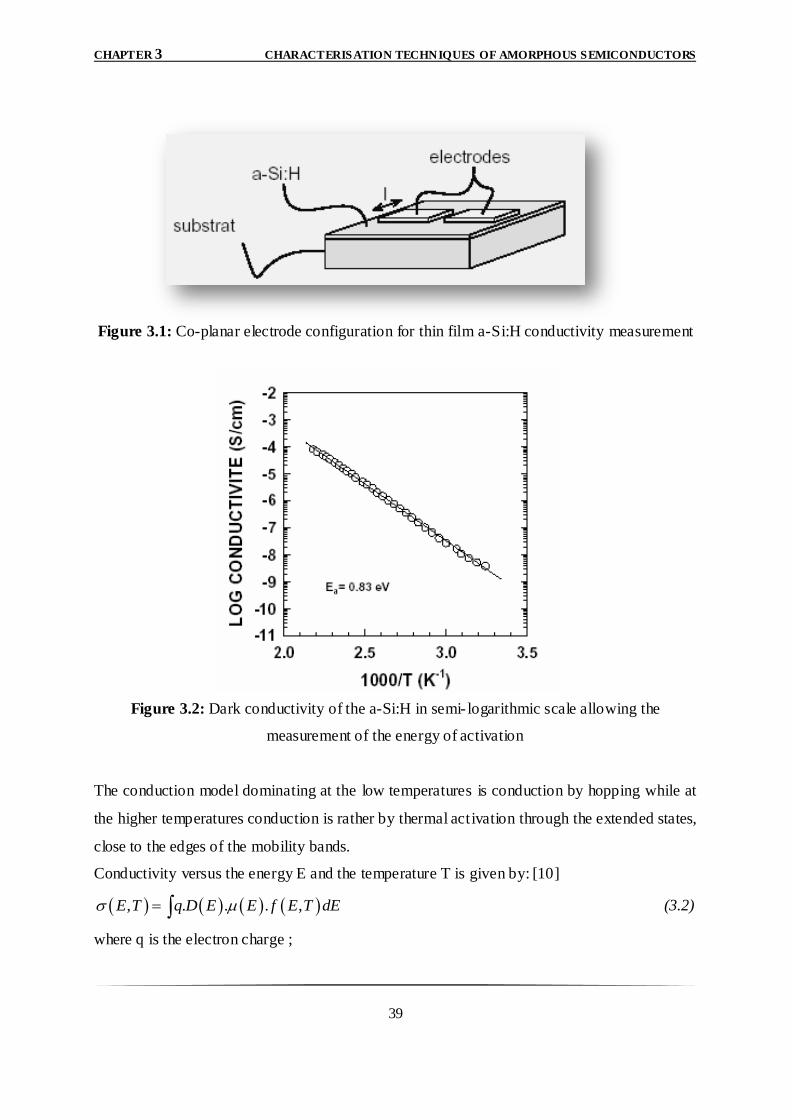
CHAPTER 3 CHARACTERISATION TECHNIQUES OF AMORPHOUS SEMICONDUCTORS
39
Figure 3.1: Co-planar electrode configuration for thin film a-Si:H conductivity measurement
Figure 3.2: Dark conductivity of the a-Si:H in semi- logarithmic scale allowing the
measurement of the energy of activation
The conduction model dominating at the low temperatures is conduction by hopping while at
the higher temperatures conduction is rather by thermal activation through the extended states,
close to the edges of the mobility bands.
Conductivity versus the energy E and the temperature T is given by: [10]
, . . . ,E T q D E E f E T dE (3.2)
where q is the electron charge ;
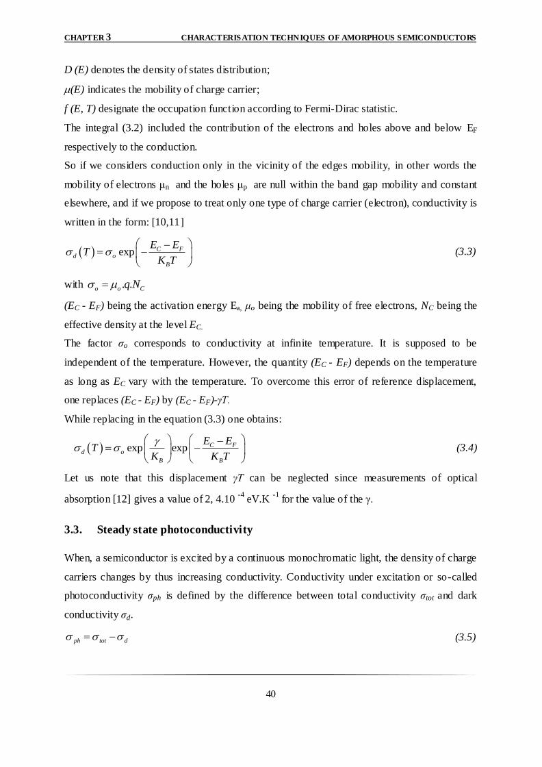
CHAPTER 3 CHARACTERISATION TECHNIQUES OF AMORPHOUS SEMICONDUCTORS
40
D (E) denotes the density of states distribution;
(E) indicates the mobility of charge carrier;
f (E, T) designate the occupation function according to Fermi-Dirac statistic.
The integral (3.2) included the contribution of the electrons and holes above and below EF
respectively to the conduction.
So if we considers conduction only in the vicinity of the edges mobility, in other words the
mobility of electrons μn and the holes μp are null within the band gap mobility and constant
elsewhere, and if we propose to treat only one type of charge carrier (electron), conductivity is
written in the form: [10,11]
exp C Fd o
B
E ET
K T
(3.3)
with . .o o Cq N
(EC - EF) being the activation energy Ea, μo being the mobility of free electrons, NC being the
effective density at the level EC.
The factor σo corresponds to conductivity at infinite temperature. It is supposed to be
independent of the temperature. However, the quantity (EC - EF) depends on the temperature
as long as EC vary with the temperature. To overcome this error of reference displacement,
one replaces (EC - EF) by (EC - EF)-γT.
While replacing in the equation (3.3) one obtains:
exp exp C Fd o
B B
E ET
K K T
(3.4)
Let us note that this displacement γT can be neglected since measurements of optical
absorption [12] gives a value of 2, 4.10 -4
eV.K -1
for the value of the γ.
3.3. Steady state photoconductivity
When, a semiconductor is excited by a continuous monochromatic light, the density of charge
carriers changes by thus increasing conductivity. Conductivity under excitation or so-called
photoconductivity σph is defined by the difference between total conductivity σtot and dark
conductivity σd.
ph tot d (3.5)
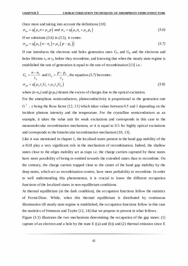
CHAPTER 3 CHARACTERISATION TECHNIQUES OF AMORPHOUS SEMICONDUCTORS
41
Once more and taking into account the definitions [10]:
0 and tot n p d n o pq n p q n p (3.6)
If we substitute (3.6) in (3.5), it comes:
0 ph n o pq n n p p (3.7)
If one introduces the electrons and holes generation rates Gn and Gp and the electrons and
holes lifetime τn et τp before they recombine, and knowing that when the steady state regime is
established the rate of generation is equal to the rate of recombination [13] i.e.:
and o on p
n p
n n p pG G
, the equation (3.7) becomes:
ph n n n p p pq G G (3.8)
where (n-no) and (p-po) denote the excess of charges due to the optical excitation.
For the amorphous semiconductors, photoconductivity is proportional to the generation rate
G γ
, γ being the Rose factor [12, 13] which takes values between 0.5 and 1 depending on the
incident photons intensity and the temperature. For the crystalline semiconductors as an
example, it takes the value unit for weak excitations and corresponds in this case to the
monomolecular recombination mechanism, or it is equal to 0.5 for highly optical excitations
and corresponds to the bimolecular recombination mechanism [10, 13].
Like it was mentioned in chapter 1, the localized states present in the band gap mobility of the
a-Si:H play a very significant role in the mechanism of recombination. Indeed, the shallow
states close to the edges mobility act as traps i.e. the charge carriers captured by these states
have more possibility of being re-emitted towards the extended states than to recombine. On
the contrary, the charge carriers trapped close to the center of the band gap mobility by the
deep states, which act as recombination centers, have more probability to recombine. In order
to well understanding this phenomenon, it is crucial to know the different occupation
functions of the localized states in non-equilibrium conditions.
At thermal equilibrium (in the dark condition), the occupation functions follow the statistics
of Fermi-Dirac. While, when this thermal equilibrium is distributed by continuous
illumination till steady state regime is established, the occupation functions follow in this case
the statistics of Simmons and Taylor [12, 14] that we propose to present in what fo llows.
Figure (3.3) illustrates the two mechanisms determining the occupation of the gap states: (1)
capture of an electron and a hole by the state E ((a) and (b)) and (2) thermal emission since E
CHAPTER 3 CHARACTERISATION TECHNIQUES OF AMORPHOUS SEMICONDUCTORS
42
towards the nearest extended band ((c) and (d)). In steady state condition the sum of the rates
(a) and (b) must be equal to the sum of the rates (c) and (d).
Figure 3.3: Mechanisms of capture and emission
The occupation function is given by [12]:
n p
n n p p
nC pCf E
nC e E pC e E
(3.9)
Firstly, let us consider the case of the localized states behaving rather as centers of
recombination where the capture coefficient is much higher than the emission coefficient. We
define the relative capture coefficient r(S) at energy E for each type of state S by:
,
,
n
p
C S Er S
C S E (3.10)
That means all the states of the type S having the same ratio r(S) have the same occupation
function independently of their absolute values of capture Cn and Cp and their positions E.
Hence, the function of occupation f becomes then:
r S nf
r S n p
(3.11)
Electron
emission
e
Electron
capture
e
Hole
emission
e
Hole
capture
e
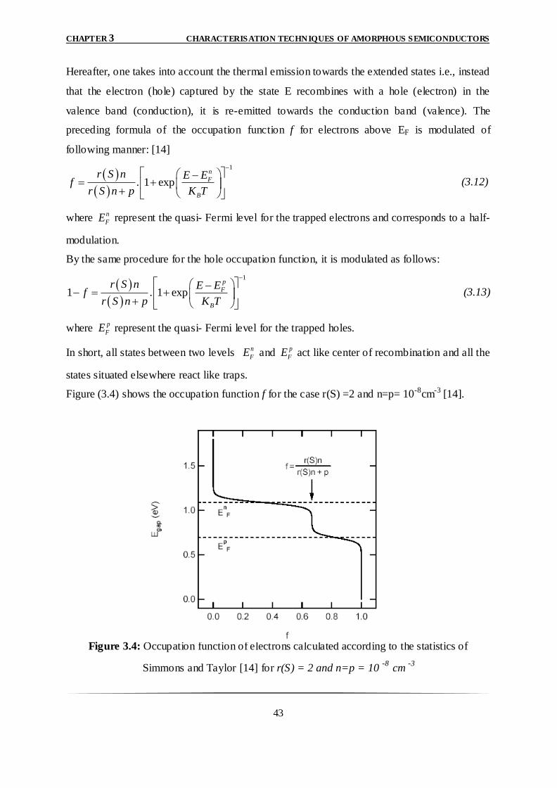
CHAPTER 3 CHARACTERISATION TECHNIQUES OF AMORPHOUS SEMICONDUCTORS
43
Hereafter, one takes into account the thermal emission towards the extended states i.e., instead
that the electron (hole) captured by the state E recombines with a hole (electron) in the
valence band (conduction), it is re-emitted towards the conduction band (valence). The
preceding formula of the occupation function f for electrons above EF is modulated of
following manner: [14]
1
. 1 expn
F
B
r S n E Ef
r S n p K T
(3.12)
where n
FE represent the quasi- Fermi level for the trapped electrons and corresponds to a half-
modulation.
By the same procedure for the hole occupation function, it is modulated as follows:
1
1 . 1 expp
F
B
r S n E Ef
r S n p K T
(3.13)
where p
FE represent the quasi- Fermi level for the trapped holes.
In short, all states between two levels n
FE and p
FE act like center of recombination and all the
states situated elsewhere react like traps.
Figure (3.4) shows the occupation function f for the case r(S) =2 and n=p= 10-8cm-3 [14].
Figure 3.4: Occupation function of electrons calculated according to the statistics of
Simmons and Taylor [14] for r(S) = 2 and n=p = 10 -8
cm -3
CHAPTER 3 CHARACTERISATION TECHNIQUES OF AMORPHOUS SEMICONDUCTORS
44
If the optical excitation is periodic the response of the amorphous semiconductor, so-called
modulated photoconductivity, is also periodic but with a delay of phase compared to the
excitation which in turn depends on the frequency of excitation. The phenomenon of
recombination in this case occurs after a multi-trapping process of the charge carriers which
are held during a time τR defined as recombination time. We will review this point in the next
chapter.
3.4. Constant photocurrent measurement
We will present in what follows a detail study of the CPM method and in the following
chapters we will focus on modeling side of this technique.
The technique of constant photocurrent or CPM was introduced by Vanecek et al. [20]. The
basic idea of the constant photocurrent technique is to adjust the photon flux h of such
manner that photoconductivity remains constant through the sample for all incident photons
energy h Under these conditions, one ensures that the occupation of the electronic states is
constant as well as the concentration of the photo-generated carriers. Under these
circumstances, the product remains constant for all used wavelengths λ. CPM experiment
allows us to measure weak absorption corresponding to the deep defects. This makes possible
to deduce the nature and the energy distribution of the deep defects in the gap starting from
the measurement of the optical absorption coefficient (h). The exponential region of the
absorption in the valence band tail is also referred to as the Urbach regime, as was already
indicated in section 2.2. The inverse logarithmic slope of the absorption coefficient in this
regime is denoted as the Urbach energy E0.
The defect density is calculated from the value of at the intersection of the weakly
increasing contribution of the deep defect states, and the exponentially increasing contribution
of the valence band tail states. For this, a proportionality constant of 1016 cm-2 is usually used
[51]. CPM experiment has the advantage compared to technique PDS (see next item) of being
insensitive to the surface defects.
Figure 3.9 illustrates an example of set up used for the optical absorption measurement by the
constant photocurrent method.
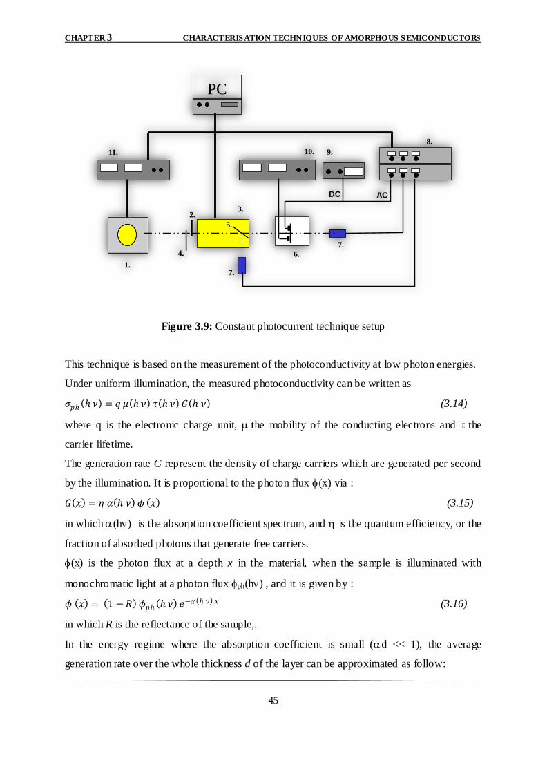
CHAPTER 3 CHARACTERISATION TECHNIQUES OF AMORPHOUS SEMICONDUCTORS
45
Figure 3.9: Constant photocurrent technique setup
This technique is based on the measurement of the photoconductivity at low photon energies.
Under uniform illumination, the measured photoconductivity can be written as
𝜎𝑝ℎ ℎ 𝜈 = 𝑞 𝜇 ℎ 𝜈 𝜏 ℎ 𝜈 𝐺 ℎ 𝜈 (3.14)
where q is the electronic charge unit, the mobility of the conducting electrons and the
carrier lifetime.
The generation rate G represent the density of charge carriers which are generated per second
by the illumination. It is proportional to the photon flux (x) via :
𝐺 𝑥 = 𝜂 𝛼 ℎ 𝜈 𝜙 𝑥 (3.15)
in which (h) is the absorption coefficient spectrum, and is the quantum efficiency, or the
fraction of absorbed photons that generate free carriers.
(x) is the photon flux at a depth x in the material, when the sample is illuminated with
monochromatic light at a photon flux_ ph(h) , and it is given by :
𝜙 𝑥 = 1 −𝑅 𝜙𝑝ℎ ℎ 𝜈 𝑒−𝛼 ℎ 𝜈 𝑥 � (3.16)
in which R is the reflectance of the sample,.
In the energy regime where the absorption coefficient is small (d << 1), the average
generation rate over the whole thickness d of the layer can be approximated as follow:
1.
2.3.
4.
5.
7.
10.11.
6.
7.
8.
PC
DC AC
9.
CHAPTER 3 CHARACTERISATION TECHNIQUES OF AMORPHOUS SEMICONDUCTORS
46
𝐺 ℎ 𝜈 = 𝜂 1 − 𝑅 𝜙𝑝ℎ ℎ 𝜈 𝛼 ℎ 𝜈 _ (3.17)
Knowing that 𝜎𝑝ℎ = 𝐼𝑝ℎ 𝑤
𝑉 𝑙 𝑑 , the photocurrent can be now given by
𝐼𝑝ℎ ℎ 𝜈 = 𝑞 𝑙 𝑑
𝑤 𝑉 1 −𝑅 𝜂 𝜇 𝜏 ℎ 𝜈 𝜙𝑝ℎ ℎ 𝜈 𝛼 ℎ 𝜈 (3.18)
in which l is the width of the electrodes, w the distance between the electrodes , V the applied
voltage, and d the thickness of the film.
The lifetime of the charge carriers is dependent on the recombination rate of the free
carriers. However, when the photocurrent is kept constant for all monochromatic photon
energies h, the carrier lifetime is, in good approximation, also constant. Furthermore, the
mobility is assumed to be constant.
Due to the optical thickness of the thin films, interference fringes appear in the experimental
absorption spectrum. As the intensity of the transmitted light and reflected light was not
measured, the term (1-R) in equation (3.18) is assumed to be constant, and no correction is
made for the presence of the interference fringes [50]. These fringes can, in first
approximation, be averaged out from the absorption spectrum.
The reflectivity R is usually supposed to be null and quantum efficiency η is considered equal
to the unit, the equation (3.18) is reduced then to:
.G h h h (3.19)
As G ( h ) is constant, the resulting absorption coefficient is dependent only on the incident
photon flux and given by _
1
h h Cte hh
(3.20)
where C is an energy independent constant. This constant, and thus the absorption coefficient
(h), is calibrated with the absolute absorption coefficient obtained from
reflection/transmission measurements or from PDS measurements (see next item).
Nevertheless, absolute values of (h) can be obtained directly by using absolute technique
CPM experiment. This technique is the combination of the standard CPM and the
transmission CPM where a second detector is placed behind the sample [21, 22].
In the end, this technique can be configured in the continuous mode (DC mode) [23], or in the
periodic mode (AC mode) [24, 25, 26]; both are largely used. This subject will be covered in
chapter 4 and 5.
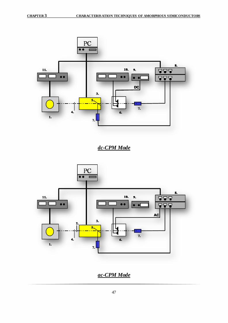
CHAPTER 3 CHARACTERISATION TECHNIQUES OF AMORPHOUS SEMICONDUCTORS
47
dc-CPM Mode
ac-CPM Mode
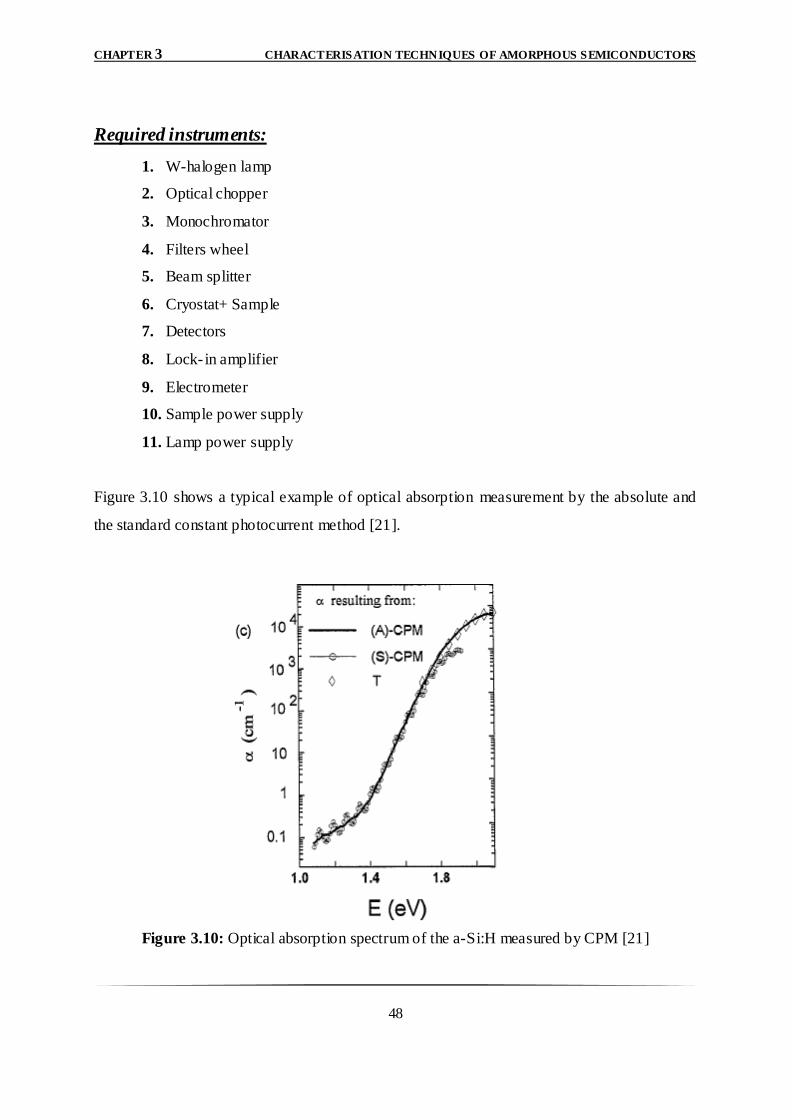
CHAPTER 3 CHARACTERISATION TECHNIQUES OF AMORPHOUS SEMICONDUCTORS
48
Required instruments:
1. W-halogen lamp
2. Optical chopper
3. Monochromator
4. Filters wheel
5. Beam splitter
6. Cryostat+ Sample
7. Detectors
8. Lock- in amplifier
9. Electrometer
10. Sample power supply
11. Lamp power supply
Figure 3.10 shows a typical example of optical absorption measurement by the absolute and
the standard constant photocurrent method [21].
Figure 3.10: Optical absorption spectrum of the a-Si:H measured by CPM [21]
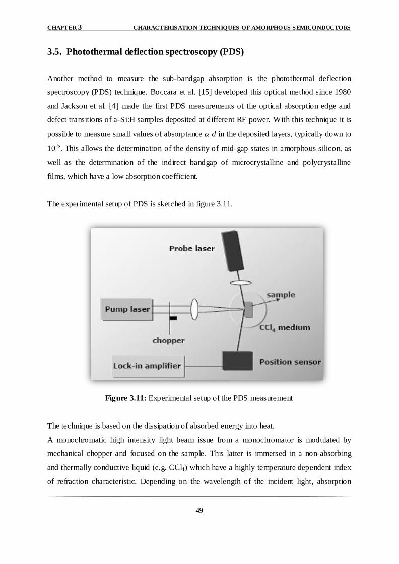
CHAPTER 3 CHARACTERISATION TECHNIQUES OF AMORPHOUS SEMICONDUCTORS
49
3.5. Photothermal deflection spectroscopy (PDS)
Another method to measure the sub-bandgap absorption is the photothermal deflection
spectroscopy (PDS) technique. Boccara et al. [15] developed this optical method since 1980
and Jackson et al. [4] made the first PDS measurements of the optical absorption edge and
defect transitions of a-Si:H samples deposited at different RF power. With this technique it is
possible to measure small values of absorptance d in the deposited layers, typically down to
10-5. This allows the determination of the density of mid-gap states in amorphous silicon, as
well as the determination of the indirect bandgap of microcrystalline and polycrystalline
films, which have a low absorption coefficient.
The experimental setup of PDS is sketched in figure 3.11.
Figure 3.11: Experimental setup of the PDS measurement
The technique is based on the dissipation of absorbed energy into heat.
A monochromatic high intensity light beam issue from a monochromator is modulated by
mechanical chopper and focused on the sample. This latter is immersed in a non-absorbing
and thermally conductive liquid (e.g. CCl4) which have a highly temperature dependent index
of refraction characteristic. Depending on the wavelength of the incident light, absorption
CHAPTER 3 CHARACTERISATION TECHNIQUES OF AMORPHOUS SEMICONDUCTORS
50
may occur. The absorbed energy is subsequently dissipated into heat in the surrounding
liquid, a gradient change in the refractive index of the liquid close to the sample surface is
established. As a result, a laser beam (e.g. He-Ne laser) directed parallel to the sample surface
is deflected. The deflection signal is measured by a position sensitive detector, which is
connected to a lock- in amplifier.
The angle of deflection of the probe beam is found to be proportional to the absorption
coefficient [53]. Knowing the film thickness d and the appropriate value of derivative of the
refractive index of the liquid with respect to the temperature 𝑑 𝑛
𝑑 𝑇 , the spectral dependence of
the absorption coefficient (h) can be calculated according to the equation [53]:
Δ 𝜃 ∝ 𝐿 𝑑 𝑛
𝑑 𝑇 𝐼𝑜 𝛼 𝑑 (3.21)
in which L is the width of the pump beam spot parallel to the direction of the laser beam and I0
is the pump beam intensity.
Measuring both the deflection of the laser beam and the intensity of the monochromatic pump
beam at different wavelengths thus yields a relative absorption spectrum of the material. For
short wavelengths, all light is absorbed in the film and the absorption spectrum becomes flat
where d ≥ 1. To obtain absolute absorption spectra, the data were scaled either to the (h)
data from reflection/transmission measurements, or to the region where d equals 1. The
indirect optical bandgap of microcrystalline and polycrystalline silicon can be derived from a
plot of 𝛼 versus h.
This measurement is widely used in the field of amorphous silicon, it is used to estimate the
density of defects since a proportionality exists between optical absorption coefficient and the
density of defects where absorption is controlled by the transitions between these defects and
the extended bands. These transitions are excited by photons of energy lower than the
mobility band gap width. According to the method suggested by Wyrsch [17], one can deduce
the density of defects by multiplying absorption at 1.2eV by a factor of calibration equal to
2.1016 cm2:
162.10 dh N (3.22)
Although the CPM and PDS techniques are both used to measure the sub-bandgap absorption,
the defect absorption measured in the case of PDS is significantly larger than in the case of
CPM. The Urbach tail, however, is identical for both techniques. The difference in defect
absorption has often been attributed to the contribution of surface defect states or of the
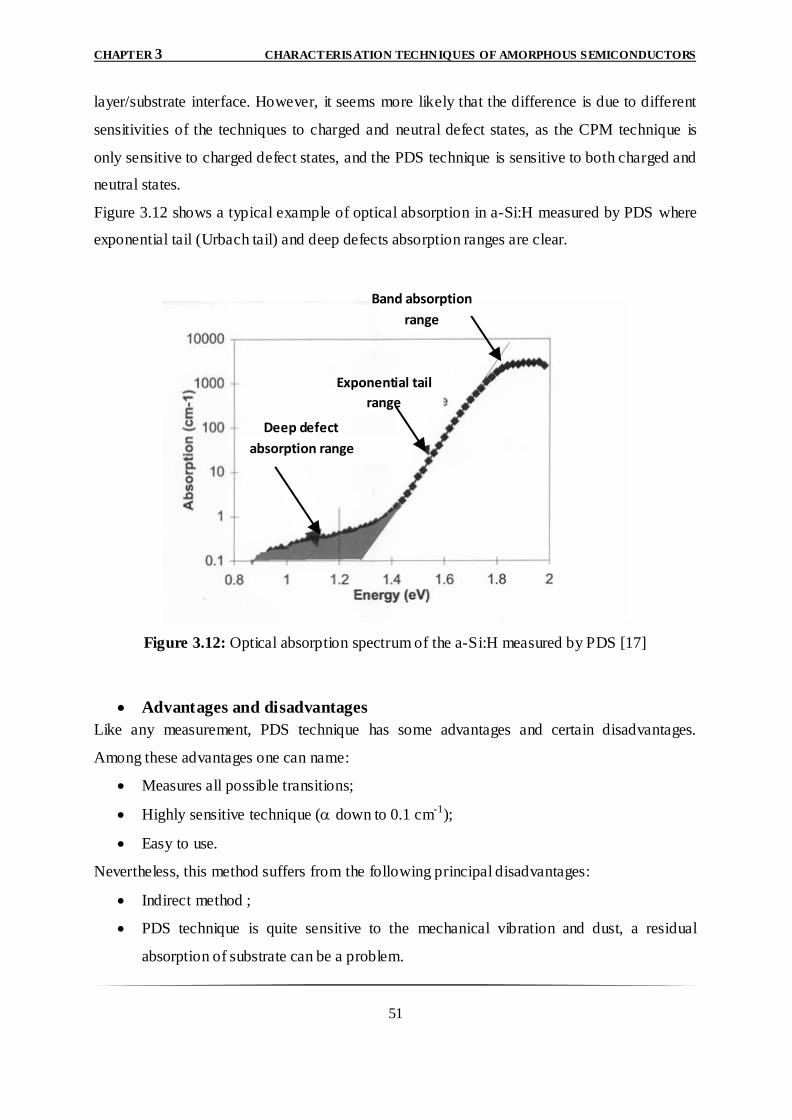
CHAPTER 3 CHARACTERISATION TECHNIQUES OF AMORPHOUS SEMICONDUCTORS
51
layer/substrate interface. However, it seems more likely that the difference is due to different
sensitivities of the techniques to charged and neutral defect states, as the CPM technique is
only sensitive to charged defect states, and the PDS technique is sensitive to both charged and
neutral states.
Figure 3.12 shows a typical example of optical absorption in a-Si:H measured by PDS where
exponential tail (Urbach tail) and deep defects absorption ranges are clear.
Figure 3.12: Optical absorption spectrum of the a-Si:H measured by PDS [17]
Advantages and disadvantages
Like any measurement, PDS technique has some advantages and certain disadvantages.
Among these advantages one can name:
Measures all possible transitions;
Highly sensitive technique ( down to 0.1 cm-1);
Easy to use.
Nevertheless, this method suffers from the following principal disadvantages:
Indirect method ;
PDS technique is quite sensitive to the mechanical vibration and dust, a residual
absorption of substrate can be a problem.
Deep defect
absorption range
Exponential tail
range
Band absorption
range
CHAPTER 3 CHARACTERISATION TECHNIQUES OF AMORPHOUS SEMICONDUCTORS
52
Measurements must be calibrated to measurements of optical Transmission-Reflection
measurements at 1.7eV;
Sensitive to both surface/interface and bulk states especially for low thicknesses;
Measurement is influenced by the nature of the substrate; if this latter is more
absorbent than the sample (metallic contact for example), the measurement of the
optical absorption of the layer is not possible;
Measurements cannot be taken in situ i.e. during the process of film deposition;
For accurate measurement, a series of high quality films with thicknesse s > 10 m
must be investigated.
3.6. Dual beam photoconductivity (DBP)
Dual beam photoconductivity method is one of the sub-band gap absorption spectroscopy. In
this technique, two light beams AC and DC are used. In this method two beams of light AC
and DC are used. The monochromatic probe light of intensity is periodic of fixed frequency
usually of 10Hz to 1000Hz [18]. It is used to probe the band gap of the material and the
resulting photoconductivity is measured using a lock- in amplifier. The continuous bias light
of constant intensity o is used to generate free carriers by changing the occupation of the gap
states. Consequently maintaining the quasi- Fermi levels and n p
F FE E constants.
Thus, by using a range of constant flux (varied generation rates), more deep states are
occupied by the electrons (case of photoconductivity type N) what implies more transitions
towards the conduction band. As a result, the coefficient absorption is higher so easier to
detect.
The condition o must be taken into account for this technique. Under this condition,
continues excitation o (hν) and periodic photoconductivity σph (hν) resulting from the
periodic excitation, are in linear relationship with the optical absorption coefficient α (hν)
according to the following formula [19]:
.
ph
o
hh
Cte h
(3.23)
Cte being the constant of proportionality.
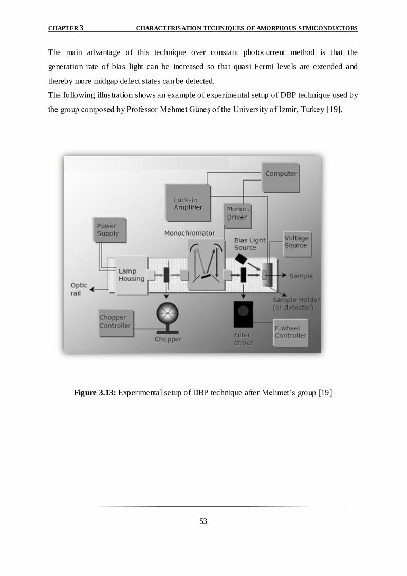
CHAPTER 3 CHARACTERISATION TECHNIQUES OF AMORPHOUS SEMICONDUCTORS
53
The main advantage of this technique over constant photocurrent method is that the
generation rate of bias light can be increased so that quasi Fermi levels are extended and
thereby more midgap defect states can be detected.
The following illustration shows an example of experimental setup of DBP technique used by
the group composed by Professor Mehmet Güneş of the University of Izmir, Turkey [19].
Figure 3.13: Experimental setup of DBP technique after Mehmet‟s group [19]
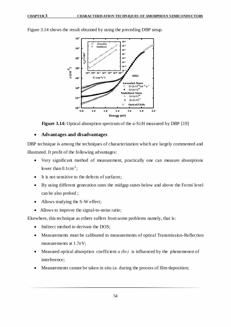
CHAPTER 3 CHARACTERISATION TECHNIQUES OF AMORPHOUS SEMICONDUCTORS
54
Figure 3.14 shows the result obtained by using the preceding DBP setup.
Figure 3.14: Optical absorption spectrum of the a-Si:H measured by DBP [19]
Advantages and disadvantages
DBP technique is among the techniques of characterization which are largely commented and
illustrated. It profit of the following advantages:
Very significant method of measurement, practically one can measure absorptions
lower than 0.1cm-1;
It is not sensitive to the defects of surfaces;
By using different generation rates the midgap states below and above the Fermi level
can be also probed ;
Allows studying the S-W effect;
Allows to improve the signal-to-noise ratio;
Elsewhere, this technique as others suffers from some problems namely, that is:
Indirect method to derivate the DOS;
Measurements must be calibrated to measurements of optical Transmission-Reflection
measurements at 1.7eV;
Measured optical absorption coefficient α (hν) is influenced by the phenomenon of
interference;
Measurements cannot be taken in situ i.e. during the process of film deposition;
CHAPTER 3 CHARACTERISATION TECHNIQUES OF AMORPHOUS SEMICONDUCTORS
55
References [1] H. Matsuura, “Electrical properties of amorphous/crystalline semiconductor eterojunctions
and determination of gap-state distributions in amorphous semiconductors”, Ph.D.thesis,
Kyoto University, Japan, 1994.
[2] A. Treatise, “Semiconductors and Semimetals”, Volume 21, Part C, Academic Press Inc.,
Orlando, Florida, USA, 1984.
[3] V. Cech and J. Stuchlik, Phys. Stat. Sol. (a) 187, No. 2, 487-491 (2001).
[4] W. B. Jackson, N. M. Amer, A. C. Boccara, and D. Fournier, Applied Optics 20(8) (1981)
1333-1344.
[5] J. S. Payson, and S. Guha, Physical Review B, Vol. 32, No.2, pp. 1326-1329, July 1985.
[6] I. –S. Chen, L. Jiao, R. W. Collins, C. R. Wronski, Journal of Non-Crystalline Solids 198-
200 (1996) 391-394.
[7] M. Günes, C. R. Wronski and T. J. McMahon, J. Appl. Phys. 76 (4), 15 August 1994.
[8] M. Vanĕček, J. Kočka, A. Poruba, and A. Fejfar, J. Appl. Phys., 78 (10), 15 November
1995.
[9] M. Sarr, J. L. Brebner, Solar Energy Materials and Solar Cells 70 (2002), 459-467.
[10] R. A. Street, “Hydrogenated amorphous silicon”, Cambridge university press, 1991.
[11] M. F. Thorpe and L. Tichy, “Properties and Applications of Amorphous Materials”,
Proceedings of NATO Advanced Study Institute, Czech Republic, 25 June-7 July 2000.
[12] D. P. Webb, “Optoelectronic properties of amorphous semiconductors”, Ph.D.thesis,
University of Abertay, Dundee, UK, October 1994.
[13] A. Merazga, “Steady state and transient photoconductivity in n-type a-Si”, Ph.D.thesis,
Dundee Institute of Technology, Dundee, UK, 1990.
[14] S. Heck, “Investigation of light- induced defects in hydrogenated amorphous silicon by
low temperature annealing and pulsed degradation”, PhD Thesis, der Philipps-Universitat
Marburg, Marburg/Lahn 2002.
[15] A. C. Boccara, D. Fournier, J. Badoz, Appl. Phys. Lett. 36 (2), 130 (1980).
[16] T. Searle, “Properties of Amorphous Silicon and its Alloys”, Edited by University of
Sheffield, UK, 1998.
CHAPTER 3 CHARACTERISATION TECHNIQUES OF AMORPHOUS SEMICONDUCTORS
56
[17] Patrick Chabloz, “Les couches épaisses en silicium amorphe, application comme
détecteurs de rayon X”, Thèse N 1485, Ecole polytechnique fédérale de Lausanne,
France,1996.
[18] S. Lee, S. Kumar, C. R. Wronski, N. Maley, Journal of Non-Crystalline Solids 114
(1989) 316-318.
[19] M. Günes, C. R. Wronski, J. Appl. Phys. Vol. 81, No. 8, 15 April 1997.
[20] A. Třĭska, I. Shimizu, J. Kočka, L. Tichŷ and M. Vanĕček, Journal of Non-Crystalline
Solids 59-60 (1983) 493-496.
[21] A. Fejfar, A. Poruba, M. Vanĕček, and J. Kočka, Journal of Non-Crystalline Solids 198-
200 (1996) 304-308.
[22] K. Haenen, “Optoelectronic study of phosphorous-doped n-type and hydrogen-doped p-
type CVD diamond films”, Ph.D.thesis, Limburgs Universitair Centrum, Belgium, 2002.
[23] J. A. Schmidt and F. A. Rubinelli , J. Appl. Phys., 83 (1), 339 (1998).
[24] P. Sladek and M. L. Theye , Solid State Comms. Vol.89, No. 3, pp.199, 1994.
[25] S. Hasegawa, S. Nitta and S. Nonomura, Journal of Non Crystalline Solids 198-200
(1996) 544-547 .
[26] C. Main, S. Reynolds, I. Zrinscak and A. Merazga, Journal of Materials Science-
Materials in Electronics, 2003.
CHAPTER 4. CONSTANT PHOTOCURRENT TECHNIQUE: THEORY AND MODELING
57
CHAPTER 4
CONSTANT PHOTOCURRENT TECHNIQUE: THEORY AND
MODELING
4.1. Introduction
Constant photocurrent method was introduced in the field of a-Si:H by Vanecek et al [1] and
since then it has been widely used to investigate the density of dangling bonds defects of
many other amorphous and composite thin films as amorphous-nanocrystalline, amorphous-
microcrystalline, diamond-like carbon, etc [2]. A diverse numerical model has been
developed to simulate CPM spectrum taking into account the position of the Fermi energy
level and the full set of optical transition between localized and extended states under sub-
band-gap optical excitation, capture, emission and recombination processes [3-6]. Explanation
and modeling in the literature assume that CPM gives information about the density of
localized gap states in amorphous silicon that is the valence band tail, the integrated defect
density, the energy defect distribution and the charge state of the defect states.
Following a review on the most important theoretical points of the CPM method, attention is
devoted to the numerical modeling of the DC-CPM and AC-CPM to get more information
needed for the determination of the defect densities in the gap energy of semiconductors
materials and for the interpretation of the large discrepancy between the DC and AC constant
photocurrent method.
4.2. Density of states distribution models In this section a description of the two existing models of the DOS in a-Si:H, as an example,
are introduced, since it will be implemented in our code program. The common part between
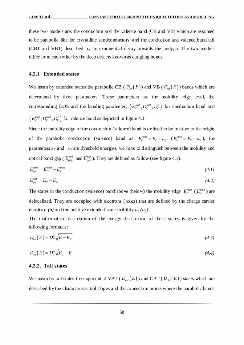
CHAPTER 4. CONSTANT PHOTOCURRENT TECHNIQUE: THEORY AND MODELING
58
these two models are: the conduction and the valence band (CB and VB) which are assumed
to be parabolic like for crystalline semiconductors, and the conduction and valence band tail
(CBT and VBT) described by an exponential decay towards the midgap. The two models
differ from each other by the deep defects known as dangling bonds.
4.2.1 Extended states
We mean by extended states the parabolic CB ( cbD E ) and VB ( vbD E ) bands which are
determined by three parameters. These parameters are the mobility edge level, the
corresponding DOS and the bending parameter; , ,mob mob o
C C CE D D for conduction band and
, ,mob mob o
V V VE D D for valence band as depicted in figure 4.1.
Since the mobility edge of the conduction (valence) band is defined to be relative to the origin
of the parabolic conduction (valence) band as mob
C C CE E ( mob
V V VE E ), the
parameters C and V are threshold energies, we have to distinguish between the mobility and
optical band gap (mob
gapE andopt
gapE ). They are defined as follow (see figure 4.1):
mob mob mob
gap C VE E E (4.1)
opt
gap C VE E E (4.2)
The states in the conduction (valence) band above (below) the mobility edge mob
CE ( mob
VE ) are
delocalized. They are occupied with electrons (holes) that are defined by the charge carrier
density n (p) and the positive extended-state mobility n (p).
The mathematical description of the energy distribution of these states is given by the
following formulas:
o
cb C CD E D E E (4.3)
o
vb V VD E D E E (4.4)
4.2.2. Tail states
We mean by tail states the exponential VBT ( vbtD E ) and CBT ( cbtD E ) states which are
described by the characteristic tail slopes and the connection points where the parabolic bands
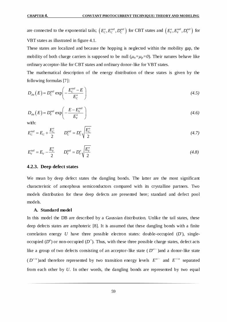
CHAPTER 4. CONSTANT PHOTOCURRENT TECHNIQUE: THEORY AND MODELING
59
are connected to the exponential tails; , ,o tail tail
C C CE E D for CBT states and , ,o tail tail
V V VE E D for
VBT states as illustrated in figure 4.1.
These states are localized and because the hopping is neglected within the mobility gap, the
mobility of both charge carriers is supposed to be null (n=p=0). Their natures behave like
ordinary acceptor- like for CBT states and ordinary donor- like for VBT states.
The mathematical description of the energy distribution of these states is given by the
following formulas [7]:
exptail
tail Ccbt C o
C
E ED E D
E
(4.5)
exptail
tail Vvbt V o
V
E ED E D
E
(4.6)
with:
2 2
o otail tail oC CC C C C
E EE E D D (4.7)
2 2
o otail tail oV VV V V V
E EE E D D (4.8)
4.2.3. Deep defect states
We mean by deep defect states the dangling bonds. The latter are the most significant
characteristic of amorphous semiconductors compared with its crystalline partners. Two
models distribution for these deep defects are presented here; standard and defect pool
models.
A. Standard model
In this model the DB are described by a Gaussian distribution. Unlike the tail states, these
deep defects states are amphoteric [8]. It is assumed that these dangling bonds with a finite
correlation energy U have three possible electron states: double-occupied (D-), single-
occupied (Do) or non-occupied (D+). Thus, with these three possible charge states, defect acts
like a group of two defects consisting of an acceptor- like state ( /oD )and a donor- like state
( /oD )and therefore represented by two transition energy levels /oE and / oE separated
from each other by U. In other words, the dangling bonds are represented by two equal
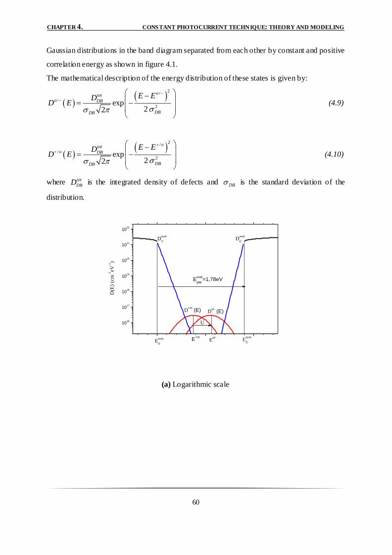
CHAPTER 4. CONSTANT PHOTOCURRENT TECHNIQUE: THEORY AND MODELING
60
Gaussian distributions in the band diagram separated from each other by constant and positive
correlation energy as shown in figure 4.1.
The mathematical description of the energy distribution of these states is given by:
2/
/
2exp
22
ototo DB
DBDB
E EDD E
(4.9)
2/
/
2exp
22
ototo DB
DBDB
E EDD E
(4.10)
where tot
DBD is the integrated density of defects and is the standard deviation of the
distribution.
1016
1017
1018
1019
1020
1021
1022
U
E+/o
Do/-
(E)D+/o
(E)
Emob
gap=1,78eV
Dmob
C
Emob
CEmob
V
Dmob
V
D(E
) (c
m-3
eV
-1)
Eo/-
(a) Logarithmic scale
DB
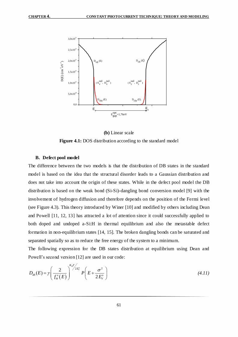
CHAPTER 4. CONSTANT PHOTOCURRENT TECHNIQUE: THEORY AND MODELING
61
0,0
5,0x10²⁰
1,0x10²¹
1,5x10²¹
2,0x10²¹
2,5x10²¹
3,0x10²¹
Dvbt
(E) Dcbt
(E)
EV
EC
Eoptgap=1,76eV
( Etail
c, D
tail
c )( E
tail
v, D
tail
v )
Dcb
(E)Dvb
(E)
D(E
) (c
m-3
eV
-1)
(b) Linear scale
Figure 4.1: DOS distribution according to the standard model
B. Defect pool model
The difference between the two models is that the distribution of DB states in the standard
model is based on the idea that the structural disorder leads to a Gaussian distribution and
does not take into account the origin of these states. While in the defect pool model the DB
distribution is based on the weak bond (Si-Si)-dangling bond conversion model [9] with the
involvement of hydrogen diffusion and therefore depends on the position of the Fermi level
(see Figure 4.3). This theory introduced by Winer [10] and modified by others including Dean
and Powell [11, 12, 13] has attracted a lot of attention since it could successfully applied to
both doped and undoped a-Si:H in thermal equilibrium and also the metastable defect
formation in non-equilibrium states [14, 15]. The broken dangling bonds can be saturated and
separated spatially so as to reduce the free energy of the system to a minimum.
The following expression for the DB states distribution at equilibrium using Dean and
Powell‟s second version [12] are used in our code:
222( )
2
BoV
K T
E
db o o
th V
D E P Ef E E
(4.11)
CHAPTER 4. CONSTANT PHOTOCURRENT TECHNIQUE: THEORY AND MODELING
62
is the scaling factor depends on the number of Si-H bonds mediating the weak-bond
breaking chemical reaction iH (iH = 0, 1 or 2), the total hydrogen concentration cH, the pool
width (standard deviation) dp and the peak position of the Gaussian distribution (defect pool
center) Ep. It is given by:
2
242 1
exp2 2 4
B
oV
K Ttail o
EV V dpHp Vo o o
V B Si Si V V
D E cE E
E K T N E E
(4.12)
denote the equilibrium occupation function of neutral dangling bond states and NSi-Si
denotes the total number of electrons in the silicon bonding states.
P (E) is the defect pool function which is described by a Gaussian distribution:
2
2
1exp
22
p
dpdp
E EP E
(4.13)
Figure 4.3 illustrates the DB states distribution according to the position of the Fermi level
which determine the peak position and the total number of dangling bonds
0,0 0,2 0,4 0,6 0,8 1,0 1,2 1,4 1,6 1,8
1015
1016
1017
1018
1019
1020
1021
1022
EF (P)
EF (i) E
F (N)
i-type
P-type
D(E
) (c
m-3
eV
-1)
E-EV (eV)
N-type
Figure 4.3: DOS distribution according to the defect pool model for intrinsic,
n and p-type a-Si:H
o
thf E
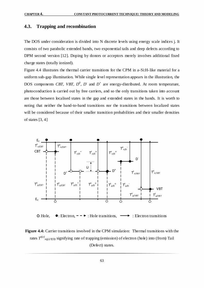
CHAPTER 4. CONSTANT PHOTOCURRENT TECHNIQUE: THEORY AND MODELING
63
4.3. Trapping and recombination
The DOS under consideration is divided into N discrete levels using energy scale indices j. It
consists of two parabolic extended bands, two exponential tails and deep defects according to
DPM second version [12]. Doping by donors or acceptors merely involves additional fixed
charge states (totally ionized).
Figure 4.4 illustrates the thermal carrier transitions for the CPM in a-Si:H-like material for a
uniform sub-gap illumination. While single level representation appears in the illustration, the
DOS components CBT, VBT, D0, D- and D+ are energy-distributed. At room temperature,
photoconduction is carried out by free carriers, and so the only transitions taken into account
are those between localised states in the gap and extended states in the bands. It is worth to
noting that neither the band-to-band transitions nor the transitions between localized states
will be considered because of their smaller transition probabilities and their smaller densities
of states [3, 4]
o: Hole, ●: Electron, : Hole transitions, : Electron transitions
Figure 4.4: Carrier transitions involved in the CPM simulation: Thermal transitions with the
rates Tt(e)n(p)/T(D) signifying rate of trapping (emission) of electron (hole) into (from) Tail
(Defect) states.
Ttn/D
+ Ttn/D
o
Ten/D
o
Ten/D
-
Ttp/D
o
Ttp/D
-
Tep/D
o
Tep/D
+
Ttn/CBT Te
n/CB T
Tep/VBT
Ttp/VB T
Tep/CB T
Ten/VBT
Tt
p/CBT
Ttn/VB T
U
EC
EV
CBT
VBT
Do
D-
D+
CHAPTER 4. CONSTANT PHOTOCURRENT TECHNIQUE: THEORY AND MODELING
64
The thermal transition rates T have the following significance:
- Tt(e)n(p)/CBT(VBT) (E): Rates of trapping (emission) of electron (hole) into (from) a level E
at the conduction band tail (valence band tail).
- Ttn/D
o(D
+) (E): Rates of electron trapping into a D0 (D+) level E at the defect states
distribution.
- Ten/D
o(D
-) (E): Rates of electron emission from a D0 (D-) level E at the defect sates
distribution.
- Ttp/D
o(D
-) (E): Rates of hole trapping into a D0 (D-) level E at the defect sates
distribution.
- Tep/D
o(D
+) (E): Rates of hole emission from a D0 (D+) level E at the defect sates
distribution.
The trapping rate is a function of free n (p) and trapped nt (pt) carrier densities following the
relation
( ) ( )( ) ( )[ ( ) ( )]t
n p n p t t tT E C n p D E n p (4.14)
where Dt (E) is the total DOS at level E and Cn(p) is the capture coefficient of the trapping
state. For trapping into D0, D- and D+ states, their respective density must replace Dt (E)-nt
(pt) in equation (4.14). Similarly, the emission rate is a function of trapped nt (pt) carrier
densities following the relation
( ) ( ) ( ) ( )( ) ( )exp ( )e
n p n p CB VB t t CB VB BT E C D n p E E k T , (4.15)
where DCB(VB) is the effective DOS at the conduction (valence) mobility edge ECB(VB) (kB is
Boltzmann constant and T the temperature). For emission from D0, D- and D+ states, their
respective density must replace nt (pt) in equation (4.15). For thermal transition expressions
detail, see appendices A and D.
In the non-equilibrium steady state, the recombination rate at any state with energy E is equal
to the difference between the total capture rate and the total re-emission rate of the electron
(or holes) via different paths. The net recombination rate via tail states is given by the same
formulae as for conventional photoconductivity simulation (Hall-Shockley-Read) with the
exception that the modified occupation functions are used. In a similar way to the band tail
situation, the recombination via dangling bond states can still be expressed as the difference
between the total trapping rate and the total emission rate from the dangling bond states,
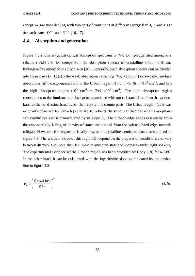
CHAPTER 4. CONSTANT PHOTOCURRENT TECHNIQUE: THEORY AND MODELING
65
except we are now dealing with two sets of transitions at different energy levels, E and E+U
for each state, /oD and /oD [16, 17].
4.4. Absorption and generation
Figure 4.5 shows a typical optical absorption spectrum (h) for hydrogenated amorphous
silicon a-Si:H and for comparison the absorption spectra of crystalline silicon c-Si and
hydrogen-free amorphous silicon a-Si [18]. Generally, such absorption spectra can be divided
into three parts [7, 18]: (i) the weak absorption region ( (h) <10 cm-1) or so-called midgap
absorption, (ii) the exponential tail, or the Urbach region (10 cm-1< (h) <103 cm-1), and (iii)
the high absorption region (103 cm-1< (h) <104 cm-1). The high absorption region
corresponds to the fundamental absorption associated with optical transitions from the valence
band to the conduction band as for their crystalline counterparts. The Urbach region (as it was
originally observed by Urbach [7] in AgBr) reflects the structural disorder of all amorphous
semiconductors and is characterized by its slope Eu. The Urbach edge arises essentially from
the exponentially falling of density of states that extend from the valence band edge towards
midgap. However, this region is ideally absent in crystalline semiconductors as sketched in
figure 4.5. The width or slope of this region Eu depend on the preparation conditions and vary
between 40 meV and more than 100 meV in annealed state and increases under light soaking.
The experimental evidence of the Urbach region has been provided by Cody [18] for a-Si:H.
In the other hand, it can be calculated with the logarithmic slope as indicated by the dashed
line in figure 4.5:
1
lnu
hE
h
(4.16)
CHAPTER 4. CONSTANT PHOTOCURRENT TECHNIQUE: THEORY AND MODELING
66
Figure 4.5: Absorption spectra of crystalline silicon (c-Si), amorphous unhydrogenated
silicon (a-Si) and hydrogenated amorphous silicon (a-Si:H,data points) [18]
The weak absorption region is related to deep gap-states and originates from Si dangling
bonds. The midgap absorption corresponds to the deep defect absorption associated with
optical transitions from localized deep states within the bandgap to extended states. These
deep defects are of prime interest for characterization of amorphous semiconductor either in
initial state (annealed state) or after bandgap illumination (degraded state) since they act as
recombination centres and their increase leads to a decrease of both dark and
photoconductivity [7, 19, 20]. Although in this region the measurements are made difficult by
the limitation on sample thickness, d, to a few microns there are several techniques which are
able to overcome this difficulty, especially the constant photocurrent method which is capable
of measuring the absorptance A down to values of about 10-5. It is worth noting that there is a
direct relation between the deep defect density in a-Si:H and Eu [18].
In its most general form, the optical absorption coefficient () where =is given by a
convolution of occupied Docc (E) and empty Dunocc (E) densities of states according to [7, 8]:
22 3
2
4
3occ unocc
o o E
Pq aD E h D E dE
n cm
(4.17a)
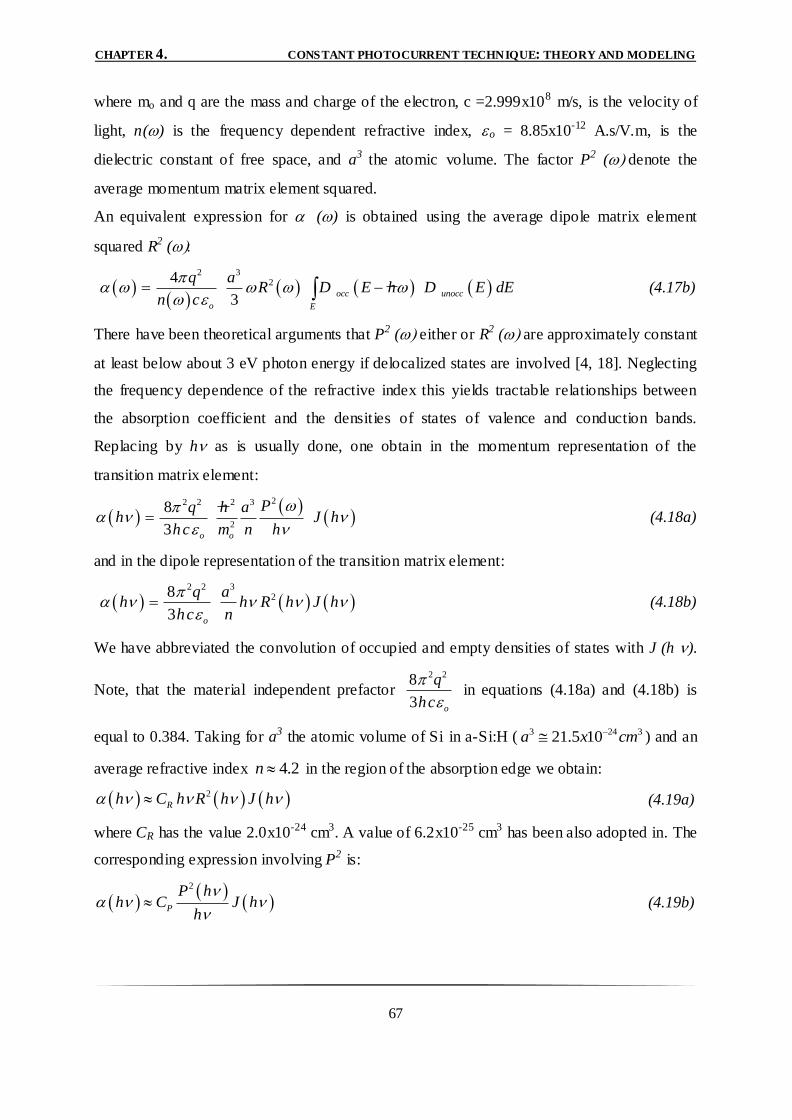
CHAPTER 4. CONSTANT PHOTOCURRENT TECHNIQUE: THEORY AND MODELING
67
where mo and q are the mass and charge of the electron, c =2.999x10⁸ m/s, is the velocity of
light, n() is the frequency dependent refractive index, o = 8.85x10⁻¹² A.s/V.m, is the
dielectric constant of free space, and a3 the atomic volume. The factor P2 (denote the
average momentum matrix element squared.
An equivalent expression for () is obtained using the average dipole matrix element
squared R2 (
2 3
24
3occ unocc
o E
q aR D E h D E dE
n c
(4.17b)
There have been theoretical arguments that P2 (either or R2 (are approximately constant
at least below about 3 eV photon energy if delocalized states are involved [4, 18]. Neglecting
the frequency dependence of the refractive index this yields tractable relationships between
the absorption coefficient and the densities of states of valence and conduction bands.
Replacing by h as is usually done, one obtain in the momentum representation of the
transition matrix element:
22 2 2 3
2
8
3 o o
Pq h ah J h
hc m n h
(4.18a)
and in the dipole representation of the transition matrix element:
2 2 3
28
3 o
q ah h R h J h
hc n
(4.18b)
We have abbreviated the convolution of occupied and empty densities of states with J (h ).
Note, that the material independent prefactor 2 28
3 o
q
hc
in equations (4.18a) and (4.18b) is
equal to 0.384. Taking for a3 the atomic volume of Si in a-Si:H ( 3 24 321.5 10a x cm ) and an
average refractive index 4.2n in the region of the absorption edge we obtain:
2
Rh C h R h J h (4.19a)
where CR has the value 2.0x10⁻²⁴ cm3. A value of 6.2x10⁻²⁵ cm3 has been also adopted in. The
corresponding expression involving P2 is:
2
P
P hh C J h
h
(4.19b)
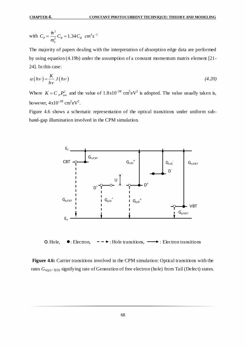
CHAPTER 4. CONSTANT PHOTOCURRENT TECHNIQUE: THEORY AND MODELING
68
with 2
4 2
21.34P R R
o
hC C C cm s
m
The majority of papers dealing with the interpretation of absorption edge data are performed
by using equation (4.19b) under the assumption of a constant momentum matrix element [21-
24]. In this case:
K
h J hh
(4.20)
Where 2
P aveK C P and the value of 1.8x10-38 cm5eV2 is adopted. The value usually taken is,
however, 4x10-38 cm5eV2.
Figure 4.6 shows a schematic representation of the optical transitions under uniform sub-
band-gap illumination involved in the CPM simulation.
o: Hole, ●: Electron, : Hole transitions, : Electron transitions
Figure 4.6: Carrier transitions involved in the CPM simulation: Optical transitions with the
rates Gn(p) / T(D) signifying rate of Generation of free electron (hole) from Tail (Defect) states.
Gp/D+
Gn/Do
Gp/Do
Gn/D-
Gp/CBT
Gn/VB T
Gp/VB T
Gn/CBT
U
EV
CBT
VBT
Do
D-
D+
EC
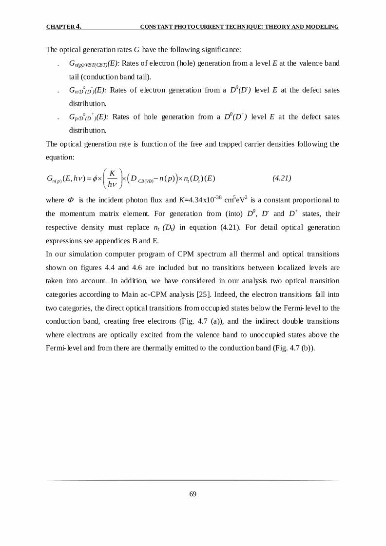
CHAPTER 4. CONSTANT PHOTOCURRENT TECHNIQUE: THEORY AND MODELING
69
The optical generation rates G have the following significance:
- Gn(p)/VBT(CBT)(E): Rates of electron (hole) generation from a level E at the valence band
tail (conduction band tail).
- Gn/Do(D
-)(E): Rates of electron generation from a D0(D-) level E at the defect sates
distribution.
- Gp/Do(D
+)(E): Rates of hole generation from a D0(D+) level E at the defect sates
distribution.
The optical generation rate is function of the free and trapped carrier densities following the
equation:
( ) ( )( , ) ( ) ( ) ( )n p CB VB t t
KG E h D n p n D E
h
(4.21)
where is the incident photon flux and K=4.34x10-38 cm5eV2 is a constant proportional to
the momentum matrix element. For generation from (into) D0, D- and D+ states, their
respective density must replace nt (Dt) in equation (4.21). For detail optical generation
expressions see appendices B and E.
In our simulation computer program of CPM spectrum all thermal and optical transitions
shown on figures 4.4 and 4.6 are included but no transitions between localized levels are
taken into account. In addition, we have considered in our analysis two optical transition
categories according to Main ac-CPM analysis [25]. Indeed, the electron transitions fall into
two categories, the direct optical transitions from occupied states below the Fermi- level to the
conduction band, creating free electrons (Fig. 4.7 (a)), and the indirect double transitions
where electrons are optically excited from the valence band to unoccupied states above the
Fermi- level and from there are thermally emitted to the conduction band (Fig. 4.7 (b)).
CHAPTER 4. CONSTANT PHOTOCURRENT TECHNIQUE: THEORY AND MODELING
70
Figure 4.7: Two optical transition categories according to Main ac-CPM analysis [25]:
(a) Direct transitions creating free electrons (●) with rate Gn(E,h).
(b) Indirect double transitions creating free holes (○): an optical transition from the
valence band to an empty state at E above EF, with rate Gp(E,h), followed by a
thermal transition from E to the conduction band with rate Ten(E).
4.5. Function occupancy
The occupation function for each level can be derived by setting the time derivate of the rate
equations for the discrete localized levels to zero. These occupation functions for the levels
have terms from sub-band-gap generation (see below) which is an evident distinction to the
occupation functions in the case of band-to-band generation. Actually three step functions U,
V and W representing the energy over which sub-band-gap generation affects localized levels
have to be used as mentioned in appendix B (cf equations (B.1)-(B.3)). For instance, if h is
the energy of the incoming photons only conduction tail states between EC - h and EC are
considered. As result occupation functions are dependent on photon energy.
4.5.1. Thermal equilibrium
At thermal equilibrium, the occupation functions of tail states (for holes in VBT and for
electrons in CBT) are given according to the Fermi-Dirac distribution function:
1
1 exp
cbt
th
F
B
f EE E
K T
(4.22)
EC
EV
(b)
(a)
EF
●
●
○
G p
G n
T e n
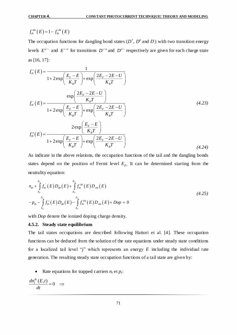
CHAPTER 4. CONSTANT PHOTOCURRENT TECHNIQUE: THEORY AND MODELING
71
1vbt cbt
th thf E f E
The occupation functions for dangling bond states (D+, Do and D-) with two transition energy
levels /oE and / oE for transitions /oD and /oD respectively are given for each charge state
as [16, 17]:
1
2 21 2exp exp
th
F F
B B
f EE E E E U
K T K T
2 2exp
2 21 2exp exp
F
B
th
F F
B B
E E U
K Tf E
E E E E U
K T K T
(4.23)
2exp
2 21 2exp exp
F
Bo
th
F F
B B
E E
K Tf E
E E E E U
K T K T
(4.24)
As indicate in the above relations, the occupation functions of the tail and the dangling bonds
states depend on the position of Fermi level EF. It can be determined starting from the
neutrality equation:
0
C C
V V
C C
V V
E E
cbt
th th db th cbt
E E
E E
vbt
th th db th vbt
E E
n f E D E f E D E
p f E D E f E D E Dop
(4.25)
with Dop denote the ionized doping charge density.
4.5.2. Steady state equilibrium
The tail states occupations are described following Hattori et al. [4]. These occupation
functions can be deduced from the solution of the rate equations under steady state conditions
for a localized tail level “j” which represents an energy E including the individual rate
generation. The resulting steady state occupation functions of a tail state are given by:
Rate equations for trapped carriers nt et pt:
0),(
dt
tEdndc
t
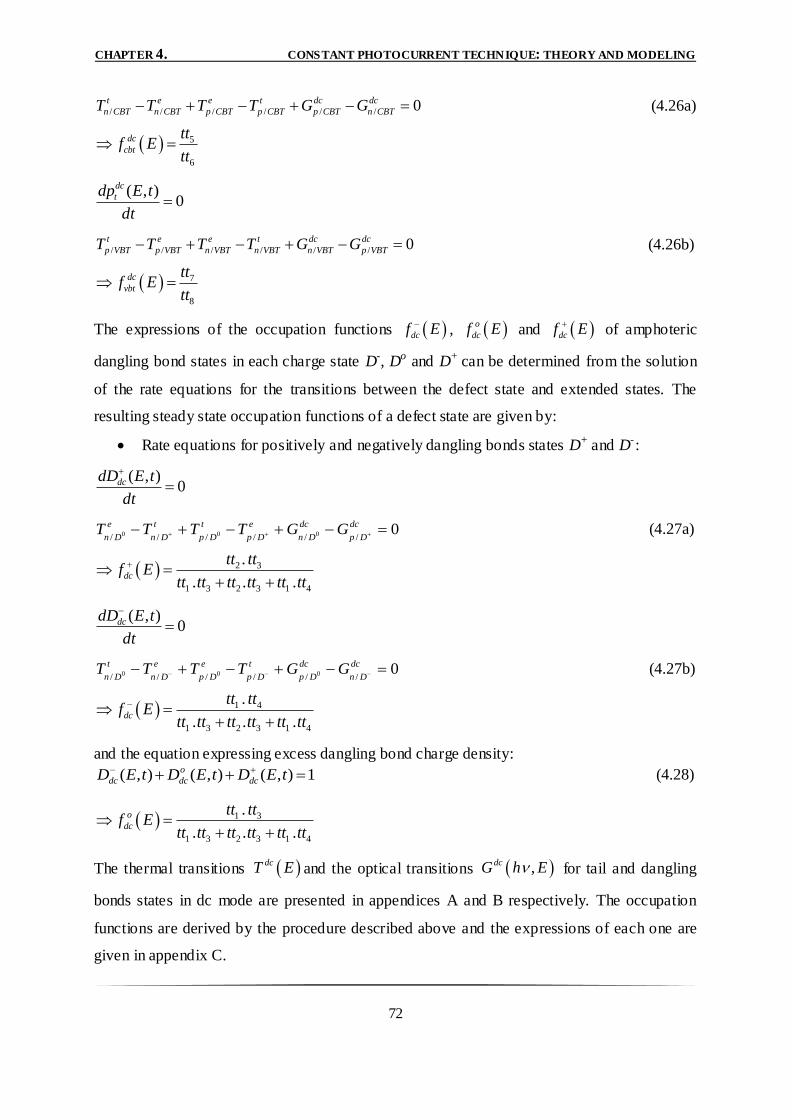
CHAPTER 4. CONSTANT PHOTOCURRENT TECHNIQUE: THEORY AND MODELING
72
/ / / / / / 0t e e t dc dc
n CBT n CBT p CBT p CBT p CBT n CBTT T T T G G (4.26a)
5
6
dc
cbt
ttf E
tt
0),(
dt
tEdpdc
t
/ / / / / / 0t e e t dc dc
p VBT p VBT n VBT n VBT n VBT p VBTT T T T G G (4.26b)
7
8
dc
vbt
ttf E
tt
The expressions of the occupation functions dcf E, o
dcf E and dcf E of amphoteric
dangling bond states in each charge state D-, Do and D+ can be determined from the solution
of the rate equations for the transitions between the defect state and extended states. The
resulting steady state occupation functions of a defect state are given by:
Rate equations for positively and negatively dangling bonds states D+ and D- :
0),(
dt
tEdDdc
0////// 000
dc
Dp
dc
Dn
e
Dp
t
Dp
t
Dn
e
DnGGTTTT
(4.27a)
2 3
1 3 2 3 1 4
.
. . .dc
tt ttf E
tt tt tt tt tt tt
0),(
dt
tEdDdc
0////// 000
dc
Dn
dc
Dp
t
Dp
e
Dp
e
Dn
t
DnGGTTTT (4.27b)
1 4
1 3 2 3 1 4
.
. . .dc
tt ttf E
tt tt tt tt tt tt
and the equation expressing excess dangling bond charge density:
1),(),(),( tEDtEDtED dc
o
dcdc (4.28)
1 3
1 3 2 3 1 4
.
. . .
o
dc
tt ttf E
tt tt tt tt tt tt
The thermal transitions dcT E and the optical transitions ,dcG h E for tail and dangling
bonds states in dc mode are presented in appendices A and B respectively. The occupation
functions are derived by the procedure described above and the expressions of each one are
given in appendix C.
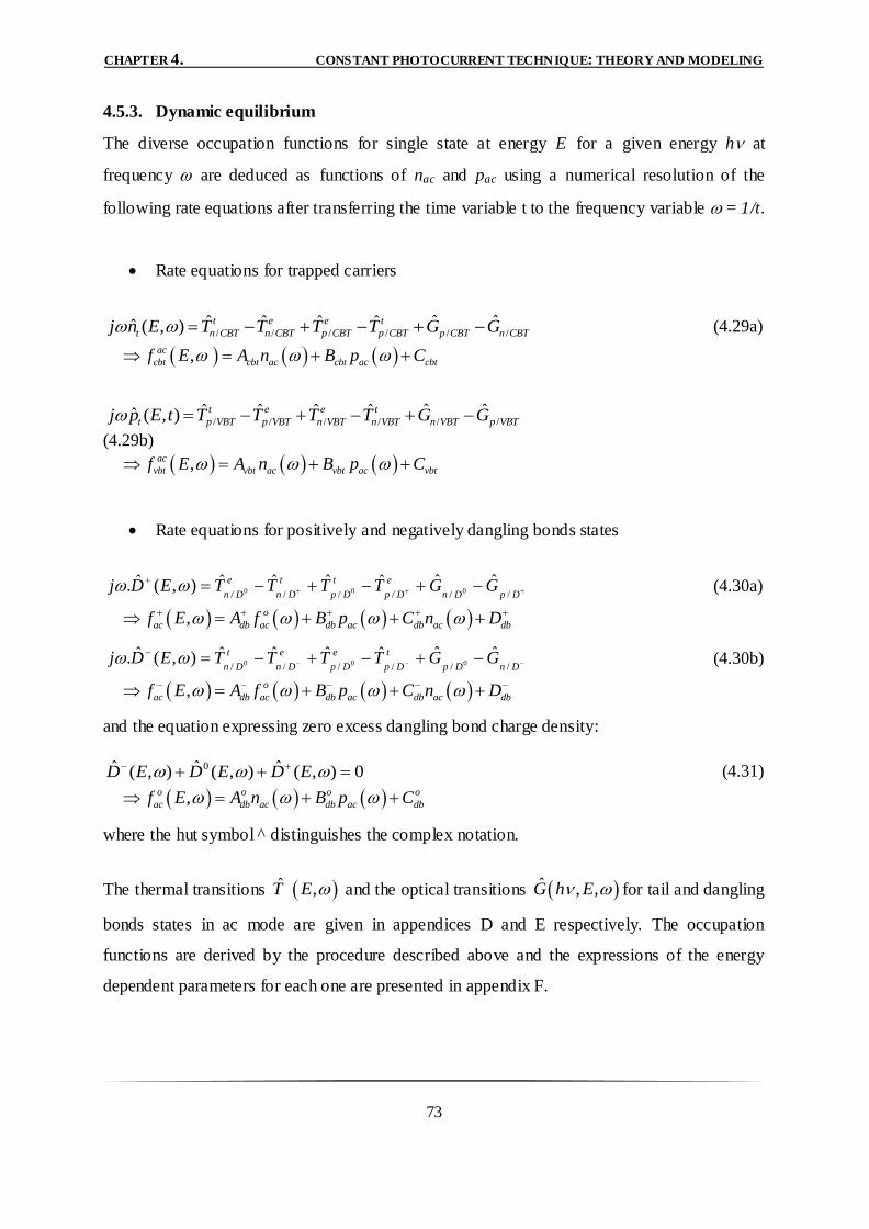
CHAPTER 4. CONSTANT PHOTOCURRENT TECHNIQUE: THEORY AND MODELING
73
4.5.3. Dynamic equilibrium
The diverse occupation functions for single state at energy E for a given energy h at
frequency are deduced as functions of nac and pac using a numerical resolution of the
following rate equations after transferring the time variable t to the frequency variable = 1/t.
Rate equations for trapped carriers
/ / / / / /ˆ ˆˆ ˆ ˆ ˆˆ ( , ) t e e t
t n CBT n CBT p CBT p CBT p CBT n CBTj n E T T T T G G (4.29a)
,ac
cbt cbt ac cbt ac cbtf E A n B p C
/ / / / / /ˆ ˆˆ ˆ ˆ ˆˆ ( , ) t e e t
t p VBT p VBT n VBT n VBT n VBT p VBTj p E t T T T T G G
(4.29b)
,ac
vbt vbt ac vbt ac vbtf E A n B p C
Rate equations for positively and negatively dangling bonds states
DpDn
e
Dp
t
Dp
t
Dn
e
DnGGTTTTEDj
//////
ˆˆˆˆˆˆ),(ˆ. 000 (4.30a)
, o
ac db ac db ac db ac dbf E A f B p C n D
DnDp
t
Dp
e
Dp
e
Dn
t
DnGGTTTTEDj
//////
ˆˆˆˆˆˆ),(ˆ. 000 (4.30b)
, o
ac db ac db ac db ac dbf E A f B p C n D
and the equation expressing zero excess dangling bond charge density:
0),(ˆ),(ˆ),(ˆ 0 EDEDED (4.31)
,o o o o
ac db ac db ac dbf E A n B p C
where the hut symbol ^ distinguishes the complex notation.
The thermal transitions ˆ ,T E and the optical transitions ˆ , ,G h E for tail and dangling
bonds states in ac mode are given in appendices D and E respectively. The occupation
functions are derived by the procedure described above and the expressions of the energy
dependent parameters for each one are presented in appendix F.
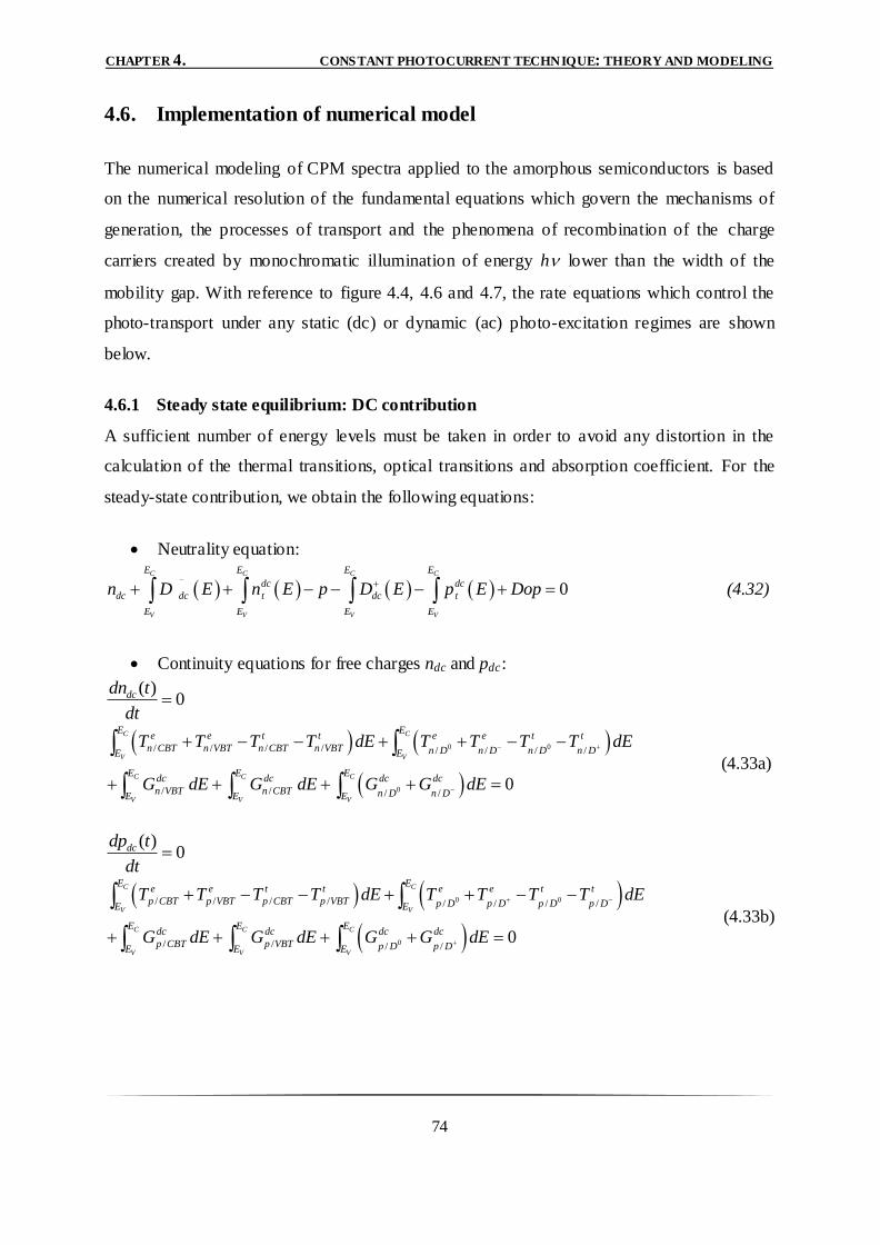
CHAPTER 4. CONSTANT PHOTOCURRENT TECHNIQUE: THEORY AND MODELING
74
4.6. Implementation of numerical model
The numerical modeling of CPM spectra applied to the amorphous semiconductors is based
on the numerical resolution of the fundamental equations which govern the mechanisms of
generation, the processes of transport and the phenomena of recombination of the charge
carriers created by monochromatic illumination of energy h lower than the width of the
mobility gap. With reference to figure 4.4, 4.6 and 4.7, the rate equations which control the
photo-transport under any static (dc) or dynamic (ac) photo-excitation regimes are shown
below.
4.6.1 Steady state equilibrium: DC contribution
A sufficient number of energy levels must be taken in order to avoid any distortion in the
calculation of the thermal transitions, optical transitions and absorption coefficient. For the
steady-state contribution, we obtain the following equations:
Neutrality equation:
0C C C C
V V V V
E E E E
dc dc
dc dc t dc t
E E E E
n D E n E p D E p E Dop (4.32)
Continuity equations for free charges ndc and pdc:
( )0dcdn t
dt
0 0
0
/ / / / / / / /
/ / / /0
C C
V V
C C C
V V V
E Ee e t t e e t t
n CBT n VBT n CBT n VBT n D n D n D n DE E
E E Edc dc dc dc
n VBT n CBT n D n DE E E
T T T T dE T T T T dE
G dE G dE G G dE
(4.33a)
( )0dcdp t
dt
0 0
0
/ / / / / / / /
/ / / /0
C C
V V
C C C
V V V
E Ee e t t e e t t
p CBT p VBT p CBT p VBT p D p D p D p DE E
E E Edc dc dc dc
p CBT p VBT p D p DE E E
T T T T dE T T T T dE
G dE G dE G G dE
(4.33b)
CHAPTER 4. CONSTANT PHOTOCURRENT TECHNIQUE: THEORY AND MODELING
75
To solve the dc-CPM equations (4.26) to (4.28) and (4.32) to (4.33), we divide the energy gap
into N closely spaced energy levels Ei, including the band edges EV=E1 and EC=EN, so that
the total number of equations to solve for the same number of variable densities (ndc, pdc, nti,
pti, Ddc+, Ddc
o and Ddc-) is 4N-2.
In modeling coplanar samples, it is a common practice to assume uniform electric field,
perfect ohmic contacts, and to neglect any transport driven by free-carrier diffusion. Under
these assumptions, the continuity equation for holes is automatically satis fied when the
continuity equation for electrons and the charge neutrality condition are fulfilled. We have
developed a computer code to solve the system of equations (4.26) to (4.28) and (4.32) to
(4.33) using appropriate numerical techniques. Our simulation of CPM spectra is based on the
starting density of states which, for a-Si:H as an example, consists of parabolic bands,
exponentially band tails and dangling bond states chosen according to the improved defect
pool model [12]. It can be separated into two principal steps. The first step and under dark
conditions, determine the position of the Fermi level from the chosen density of states and the
charge neutrality requirement, thus defining nth and pth. In the second step and under steady
state conditions, the iteration is done in two loops, an inner loop for charge neutrality and the
net recombination rate to be equal to the generation rate and an outer loop for adjusting the
photon flux of the monochromatic illumination CPM required to keep the photocurrent on a
constant level. The absorption coefficient can be then evaluated according two expressions.
The first one which is exactly the relative quantity measured in the CPM experiment, is given
by dc
CPM1
dc
h
, while the second expression which represent the absolute total
absorption coefficient, is given by dc dc dc
tot n ph h h , where dc
n h and
dc
p h corresponding to optical transitions associated, respectively, with free electron and
free hole creation, and must be taken both into account as both contribute to the absorption
processes. They are also related to the total generation rate for electrons dc
nG h and for
holes dc
pG h by dc dc
n n dcG h h and dc dc
p p dcG h h respectively. All the
thermal and optical transition rates dcT E and ,dcG E h can be deduced from equations
(4.14), (4.15) and (4.21) as follow:
CHAPTER 4. CONSTANT PHOTOCURRENT TECHNIQUE: THEORY AND MODELING
76
( ) ( )( ) ( )[ ( ) ( )]t dc dc
n p n p dc dc t t tT E C n p D E n p (4.34)
( ) ( ) ( ) ( )( ) ( )exp ( )e dc dc
n p n p CB VB t t CB VB BT E C D n p E E k T , (4.35)
( ) ( )( , ) ( ) ( )( )dc dc
n p dc CB VB dc dc t t
KG E h D n p n D E
h
(4.36)
Their mathematical formulations are given in appendices A and B.
From the simulation we can also evaluate the lifetime as functions of the photon energy by
using the following relations
dc thdc
dcnn
n nG h
h
for electron lifetime and
dc thdc
dcpp
p pG h
h
for hole lifetime.
4.6.2 Dynamic equilibrium: AC contribution
In the ac-CPM experiment the excitation photon flux (t) is a periodic function of the time
having this expression [26, 27]:
expdc act j t (4.37)
with dcbeing the constant photon flux component and ac the amplitude of an oscillatory
term having the angular frequency . In response to the photo-excitation represented by the
above equation, two types of contributions has to be considered: the first one represent the
continuous part of the excitation giving a dc photocurrent and the second one represent the
alternative part of the excitation giving an ac photocurrent. So, basically every time-
dependent physical quantities x (t), except the emission rates and the distributions of states,
are expected to have the form:
expdc acx t x x j t (4.38)
In this section, we will focus on special solutions under a sinusoidal excitation light. This is
actually the case when the photocurrent measurements are made with chopped excitation
light. We treat the case of a small ac signal and contributions from the higher order harmonics
are neglected. So, in the case of ac-CPM, the ac-photo-response requires transferring the
continuity equations (4.33a) and (4.33b) to the frequency domain using the Fourier integral.
The new equations in the frequency domain, after transferring the time variable t to the
frequency variable =1/t, are:
CHAPTER 4. CONSTANT PHOTOCURRENT TECHNIQUE: THEORY AND MODELING
77
Continuity equations for free charges nac et pac:
0 0
0
/ / / / / / / /
/ / / /
ˆ ˆ ˆ ˆ ˆ ˆ ˆ ˆˆ( )
ˆ ˆ ˆ ˆ
C C
V V
C C C
V V V
E Ee e t t e e t t
n CBT n VBT n CBT n VBT n D n D n D n DE E
E E E
n VBT n CBT n D n DE E E
j n T T T T dE T T T T dE
G dE G dE G G dE
(4.39a)
0 0
0
/ / / / / / / /
/ / / /
ˆ ˆ ˆ ˆ ˆ ˆ ˆ ˆˆ ( )
ˆ ˆ ˆ ˆ
C C
V V
C C C
V V V
E Ee e t t e e t t
p CBT p VBT p CBT p VBT p D p D p D p DE E
E E E
p CBT p VBT p D p DE E E
j p T T T T dE T T T T dE
G dE G dE G G dE
(4.39b)
Since the approximation that the total DOS at any level E is much greater than the occupied
DOS at E, particularly in the case of a small ac-signal, the rates T and G in equations (4.14),
(4.15) and (4.21) of the thermal and optical transitions are expressed in the frequency domain
as:
( ) ( )ˆ ˆ ˆ( , ) ( ) ( )[ ( )]t
n p n p tT E C D E n p (4.40)
( ) ( ) ( ) ( )ˆ ˆ ˆ( ) exp ( ) ( , )[ ( , )]e
n p n p CB VB CB VB B t tT E C D E E k T n E p E (4.41)
( ) ( )ˆ ˆ( , , ) ( , )[ ( )]n p ac CB VB t t
KG E h D n E D E
h
(4.42)
where the hut symbol ^ distinguishes the complex notation and is the magnitude of the ac
photon flux. For more details see appendices D and E.
To solve the ac-CPM equations (4.29) to (4.31) and (4.39), we divide the energy gap into N
closely spaced energy levels Ei, including the band edges EV=E1 and EC=EN, so that the total
number of equations to solve for the same number of variable densities (DDpnpn titi
ˆ,ˆ,ˆ,ˆ,ˆ,ˆ 0
and D̂ ) is 4N-2. By a similar procedure as in steady state, we can calculate all the necessary
quantities by solving the ac equations (4.29) to (4.31) and (4.39) except an extra loop
concerning frequency change is added to the procedure of simulation. So, the same kind of
relations holds for ac absorption spectra just replacing all dc quantities in by the
corresponding ac quantities.
As required by the CPM experiment, the photon energy h is varied and the ac photon flux
magnitude ac is adjusted to keep the magnitude of the ac-photoconductivity pnq pnˆˆ
CHAPTER 4. CONSTANT PHOTOCURRENT TECHNIQUE: THEORY AND MODELING
78
constant over the whole h range. The single transition ac absorption coefficient is then
deduced from equation (4.42) as:
( )
( ) ( )
ˆ ( , , )ˆ( , , ) ( , ) [ ( )]
ac n p i
n p i CB VB t i t i
ac
G E h KE h D n E D E
h
(4.43)
with tin̂ replaced by DDD ˆ,ˆ,ˆ 0 for transitions from (into) dangling bond defect states, and
the total absorption coefficient as:
( ) ( )( , ) ( , , )ac ac
n p n p i
i
h E h (4.44)
4.6.3. Deconvolution procedure
Three methods were used until now to get the DOS from a CPM experiment:
1. Pierz et al. [28] take D (E) nevertheless a constant above Ec and (1 - f (E)) =1, then
evaluated the density of filled states D (E-h) f (E-h) in a simple way by
differentiation of the (h) spectrum. This is the derivative method;
2. Kocka et al. [29] fit the experimental spectra with a chosen DOS and adjust it to get a
good agreement;
3. Jensen [30], however, introduced a correction to the derivate method assuming
parabolic energy dependence for D (E) which allows the accurate determination of the
DOS.
In this thesis and assuming that the density of unoccupied states (occupied states) at
conduction band (valence band) is constant and given by o
CD ( o
VD . the DOS distribution is
calculated from the dc or ac-absorption coefficient, after Pierz at al [28], using the derivative:
( )1
C
dc
n p
o
vh E E
d h hD E
K D d h
(4.45a)
( ) ,1
C
ac
n p
o
vh E E
d h hD E
K D d h
(4.45b)
CHAPTER 4. CONSTANT PHOTOCURRENT TECHNIQUE: THEORY AND MODELING
79
References
[1] M. Vanecek, J. Kocka, A. Poruba, and A. Fejfar, J. Appl. Phys., 78, 6203, 1995.
[2] Zdenek Remes, Ph.D. thesis, “Study of defects and microstructure of amorphous and
microcrystalline silicon thin films and polycrystalline diamond using optical methods”,
faculty of mathematics and physics, Charles university, Prague, Czech Republic, 1999.
[3] J. A. Schmidt and F. A. Rubinelli , J. Appl. Phys., 83 (1), 339 (1998).
[4] F. Siebke, H. Stiebig, A. Abo-Arais and H. Wagner, Solar Energy Materials and Solar
Cells 41/42 (1996), 529-536.
[5] R. Platz, R. Brügggemann, G. Bauer and F. R. Germany, Journal of Non-Crystalline
Solids 164-166 (1993) 355-358.
[6] K. Hattori, S. Fukuda, K. Nishimura, H. Okamoto, and Y. Hamakawa, Journal of Non-
Crystalline Solids 164-166 (1993) 351-354.
[7] A. Mettler, “Determination of the deep defect density in amorphous hydrogenated silicon
by the constant photocurrent method: A critical verification”, Ph.D. thesis, faculty of sciences,
university of Neuchatel, Switzerland (1994).
[8] R. A. Street, “Hydrogenated amorphous silicon”, Cambridge university press, 1991.
[9] M. Stutzmann, W. B. Jackson and C. C. Tsai, Physical Review B, Vol. 32, No.1, pp. 23-
47, July 1985.
[10] K. Winer, Physical Review Letters, Vol. 63, No.14, October 1989.
[11] M. J. Powell and S. C. Deane, Phys. Rev. B 48, 10815 (1993).
[12] M. J. Powell and S. C. Deane, Phys. Rev. B 53, 10121 (1996).
[13] J. Schmal, Journal of Non-Crystalline Solids 198-200 (1996) 387-390.
[14] F. Siebke, H. Stiebig, Journal of Non-Crystalline Solids 198-200 (1996) 351-354.
[15] F. Siebke, H. Stiebig, and R. Carius, Solar Energy Materials and Solar Cells 49 (1997)
7-12.
[16] W. Gao, “Computer modelling and experimental characterisation of amorphous
semiconductor thin films and devices”, PhD thesis, University of Abertay Dundee, UK, 1995.
[17] A. Merazga, “Steady state and transient photoconductivity in n-type a-Si”, Ph.D.thesis,
University of Abertay Dundee, Institute of Technology, Dundee, UK, 1990.
[18] T. Searle, “Properties of Amorphous Silicon and its Alloys”, Edited by University of
Sheffield, UK, 1998.
CHAPTER 4. CONSTANT PHOTOCURRENT TECHNIQUE: THEORY AND MODELING
80
[19] M. F. Thorpe and L. Tichy, “Properties and Applications of Amorphous Materials”,
Proceedings of NATO Advanced Study Institute, Czech Republic, 25 June-7 July 2000.
[20] A. Treatise, “Semiconductors and Semimetals”, Volume 21, Part C, Academic Press Inc.,
Orlando, Florida, USA, 1984.
[21] I. Sakata, M. Yamanaka, S. Numase, and Y. Hayashi, J. Appl. Phys. 71 (9), 4344-4353
(1992).
[22] A. Poruba and F. Schauer, Proceeding of the 8-th Inter. School on Con. Matter Phys.,
Varna, Bulgaria, 19-23 September 1994.
[23] R. Maudre, M. Maudre, S. Vignoli, P. Roca I Cabarrocas, Y. Bouizem and M. L. Theye,
Philos. Mag. B, 67(4) (1993)497-511.
[24] A. O. Kodolbaş, and Ö. Öktü, Optical Materials 20 (2002) 147-151.
[25] C. Main, S. Reynolds, I. Zrinscak and A. Merazga, Journal of Materials Science-
Materials in Electronics, 2003.
[26] H. Okamoto, H. Kida, T. Kamada, and Y. Hamakawa, Philosophical Magazine B, Vol.
52, No.6, pp. 1115-1133, 1985.
[27] C. Longeaud and J. P. Kleider, Physical Review B, Vol. 48, No.12, pp. 8715-8741,
September 1993-II.
[28] K. Pierz, B. Hilgenberg, H. Mell and G. Weiser, Journal of Non-Crystalline Solids 97-98
(1987) 63-66.
[29] J. Kocka, M. Vanecek and F. Schauer, Journal of Non-Crystalline Solids 97-98, 715
(1987).
[30] P. Jensen, Solid State Communications. Vol. 76, No. 11, pp. 1301-1303, 1990.
CHAPTER 5. CONSTANT PHOTOCURRENT TECHNIQUE: RESULTS AND DISCUSSION
81
CHAPTER 5
CONSTANT PHOTOCURRENT TECHNIQUE: RESULTS AND
DISCUSSION
5.1. Introduction
Sub-band gap absorption coefficient of amorphous semiconductors can provide useful
information on their electronic transport and optical properties. It can be used to infer the
spectral distribution of the density of gap states DOS of these materials. Many methods have
been applied in order to determine DOS but the sensitivity of each technique is not the same
in the different regions of the band gap. The most extensive are the photo deflection
spectroscopy (PDS) [1] and constant photocurrent method (CPM) [2,3] which evaluate the
density of states distribution in the lower half of the band gap and the modulated photocurrent
(MPC) [4] and time of flight in space charge limited current mode (TOF-SCLC) [5] which
evaluate it above the Fermi level.
The constant photocurrent method was originally developed for crystalline semiconductors
[6] and then applied to amorphous materials [7, 8]. This technique is based on a number of
assumptions so its applicability and its validity have often been questioned [9, 10]. Bube et al.
[11] noted that to determine the midgap defect densities the dc-CPM have to be corrected.
Mettler et al. [12] concluded that there is a “working point” at which the basic CPM
conditions are fulfilled. Zhang et al. [13] found that an inhomogeneous spatial distribution of
defects have a strong influence on the CPM determined defect density. Schmidt et al. [14]
reported that the absorption coefficient measured with dc-CPM is dependent on the constant
photocurrent chosen to perform the measurement. The constant photocurrent method can be
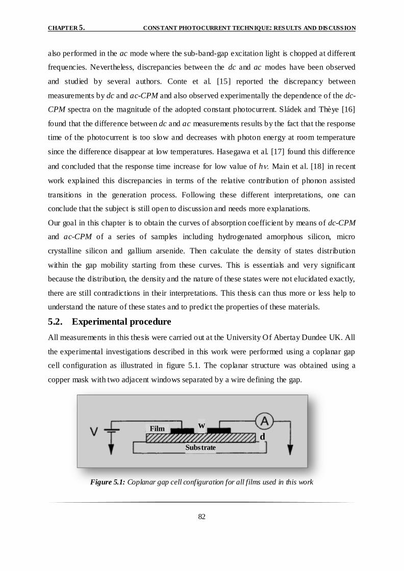
CHAPTER 5. CONSTANT PHOTOCURRENT TECHNIQUE: RESULTS AND DISCUSSION
82
also performed in the ac mode where the sub-band-gap excitation light is chopped at different
frequencies. Nevertheless, discrepancies between the dc and ac modes have been observed
and studied by several authors. Conte et al. [15] reported the discrepancy between
measurements by dc and ac-CPM and also observed experimentally the dependence of the dc-
CPM spectra on the magnitude of the adopted constant photocurrent. Sládek and Thèye [16]
found that the difference between dc and ac measurements results by the fact that the response
time of the photocurrent is too slow and decreases with photon energy at room temperature
since the difference disappear at low temperatures. Hasegawa et al. [17] found this difference
and concluded that the response time increase for low value of h Main et al. [18] in recent
work explained this discrepancies in terms of the relative contribution of phonon assisted
transitions in the generation process. Following these different interpretations, one can
conclude that the subject is still open to discussion and needs more explanations.
Our goal in this chapter is to obtain the curves of absorption coefficient by means of dc-CPM
and ac-CPM of a series of samples including hydrogenated amorphous silicon, micro
crystalline silicon and gallium arsenide. Then calculate the density of states distribution
within the gap mobility starting from these curves. This is essentials and very significant
because the distribution, the density and the nature of these states were not elucidated exactly,
there are still contradictions in their interpretations. This thesis can thus more or less help to
understand the nature of these states and to predict the properties of these materials.
5.2. Experimental procedure
All measurements in this thesis were carried out at the University Of Abertay Dundee UK. All
the experimental investigations described in this work were performed using a coplanar gap
cell configuration as illustrated in figure 5.1. The coplanar structure was obtained using a
copper mask with two adjacent windows separated by a wire defining the gap.
Figure 5.1: Coplanar gap cell configuration for all films used in this work
w
substrat
d film
Film w
Substrate
d
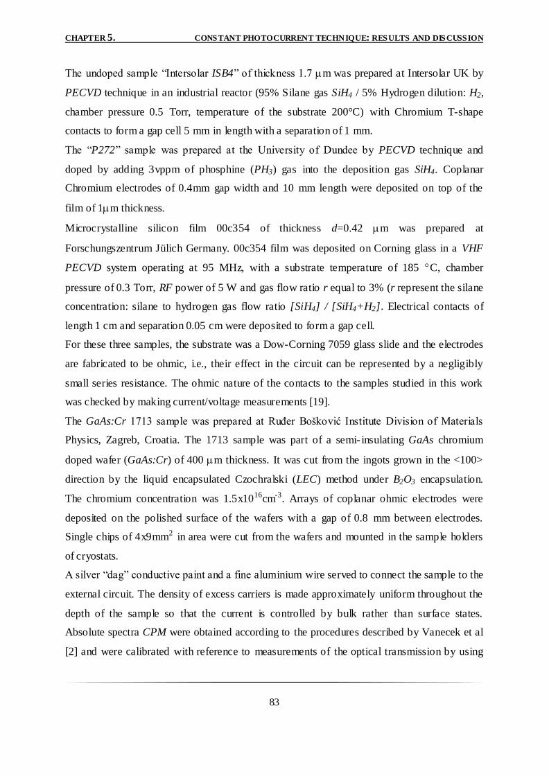
CHAPTER 5. CONSTANT PHOTOCURRENT TECHNIQUE: RESULTS AND DISCUSSION
83
The undoped sample “Intersolar ISB4” of thickness 1.7 m was prepared at Intersolar UK by
PECVD technique in an industrial reactor (95% Silane gas SiH4 / 5% Hydrogen dilution: H2,
chamber pressure 0.5 Torr, temperature of the substrate 200°C) with Chromium T-shape
contacts to form a gap cell 5 mm in length with a separation of 1 mm.
The “P272” sample was prepared at the University of Dundee by PECVD technique and
doped by adding 3vppm of phosphine (PH3) gas into the deposition gas SiH4. Coplanar
Chromium electrodes of 0.4mm gap width and 10 mm length were deposited on top of the
film of 1m thickness.
Microcrystalline silicon film 00c354 of thickness d=0.42 m was prepared at
Forschungszentrum Jülich Germany. 00c354 film was deposited on Corning glass in a VHF
PECVD system operating at 95 MHz, with a substrate temperature of 185 C, chamber
pressure of 0.3 Torr, RF power of 5 W and gas flow ratio r equal to 3% (r represent the silane
concentration: silane to hydrogen gas flow ratio [SiH4] / [SiH4+H2]. Electrical contacts of
length 1 cm and separation 0.05 cm were deposited to form a gap cell.
For these three samples, the substrate was a Dow-Corning 7059 glass slide and the electrodes
are fabricated to be ohmic, i.e., their effect in the circuit can be represented by a negligibly
small series resistance. The ohmic nature of the contacts to the samples studied in this work
was checked by making current/voltage measurements [19].
The GaAs:Cr 1713 sample was prepared at Ruđer Bošković Institute Division of Materials
Physics, Zagreb, Croatia. The 1713 sample was part of a semi- insulating GaAs chromium
doped wafer (GaAs:Cr) of 400 m thickness. It was cut from the ingots grown in the <100>
direction by the liquid encapsulated Czochralski (LEC) method under B2O3 encapsulation.
The chromium concentration was 1.5x1016cm-3. Arrays of coplanar ohmic electrodes were
deposited on the polished surface of the wafers with a gap of 0.8 mm between electrodes.
Single chips of 4x9mm2 in area were cut from the wafers and mounted in the sample holders
of cryostats.
A silver “dag” conductive paint and a fine aluminium wire served to connect the sample to the
external circuit. The density of excess carriers is made approximately uniform throughout the
depth of the sample so that the current is controlled by bulk rather than surface states.
Absolute spectra CPM were obtained according to the procedures described by Vanecek et al
[2] and were calibrated with reference to measurements of the optical transmission by using
CHAPTER 5. CONSTANT PHOTOCURRENT TECHNIQUE: RESULTS AND DISCUSSION
84
the formula of Ritter-Weiser [20]. The density of states was obtained by applying the
derivative method of Pierz et al. for each curve of absorption [21].
The details of the samples are summarized in Table 5.1, together with some of their
characteristic parameters. These parameters are given as a rough guide and are known to vary
as the history of the material unfolds. The deposition temperature was only available for
certain samples although the deposition temperatures were known to be 300oC for all the
samples.
Sample
Intersolar
ISB4
(a-Si :H)
P272
(a-Si :H)
00c354
(c-Si :H)
GaAs :Cr
1713
Length l (mm)
5
10
10
4
Gap width w (mm)
1
0.4
0.5
0.8
Thickness d (m) 1.7 1.0 0.42 400
Doping level
PH3
concentration
3vppm
chromium
concentration
1.5x1016cm-3
Dark Fermi level position
EC-EF (eV)
0.67 0.45 0.58 0.71
Room temperature currents
(A)
0.46x10⁻⁹ 26.5x10⁻⁶ 0.3x10⁻⁶ 45x10-6
Deposition temperature (°C) 200 295 185
Plasma pressure (Torr) 0.5 0.1 0.3
RF power 8 W
(40MHz)
5 W
(95MHz)
Deposition technique PECVD PECVD VHF-
PECVD
Liquid
Encapsulated
Czochralski
(LEC)
Table 5.1: Sample characteristics that are used for this investigation
CHAPTER 5. CONSTANT PHOTOCURRENT TECHNIQUE: RESULTS AND DISCUSSION
85
5.3. Dark conductivity and activation energy measurements
Two coplanar Chromium electrodes were deposited on the layers on Corning glass for all
electrical measurements. The dark current Id (T) for electric conduction was measured in
vacuum, after annealing at 200° C for at least two hours to make sure that all moisture had
evaporated from the films. A voltage V of 400V is applied during the measurement. The dark
conductivity d is calculated from:
�
𝜎𝑑 𝑇 = 𝑤 .𝐼𝑑 𝑇
𝑉.𝑙 .𝑑 (5. 1)
in which V is the applied voltage, l the width of the electrodes, w the distance between the
electrodes, and d the thickness of the film.
The energy differences between the dark Fermi energy and the conduction band (EC-EF) so-
called the activation energy Ea (or demarcation level) is calculated from the dark conductivity
d (T) using:
exp ad o
B
ET
K T
(5.2)
Usually value of 150 -200 cm [22] is given to the factor o and this is valid only for
hydrogenated amorphous silicon.
Graphically, the activation energy Ea is determined from the slope of the Arrhenius plot of the
dark conductivity versus the reciprocal temperature T ( 1000ln d fT
).
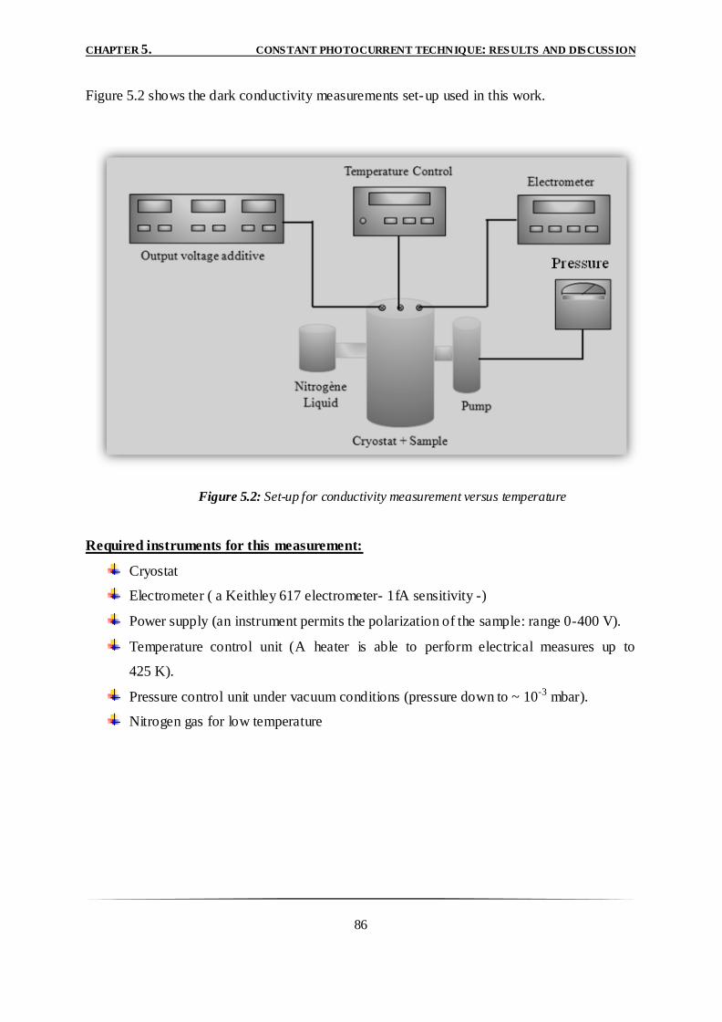
CHAPTER 5. CONSTANT PHOTOCURRENT TECHNIQUE: RESULTS AND DISCUSSION
86
Figure 5.2 shows the dark conductivity measurements set-up used in this work.
Figure 5.2: Set-up for conductivity measurement versus temperature
Required instruments for this measurement:
Cryostat
Electrometer ( a Keithley 617 electrometer- 1fA sensitivity -)
Power supply (an instrument permits the polarization of the sample: range 0-400 V).
Temperature control unit (A heater is able to perform electrical measures up to
425 K).
Pressure control unit under vacuum conditions (pressure down to ~ 10-3 mbar).
Nitrogen gas for low temperature
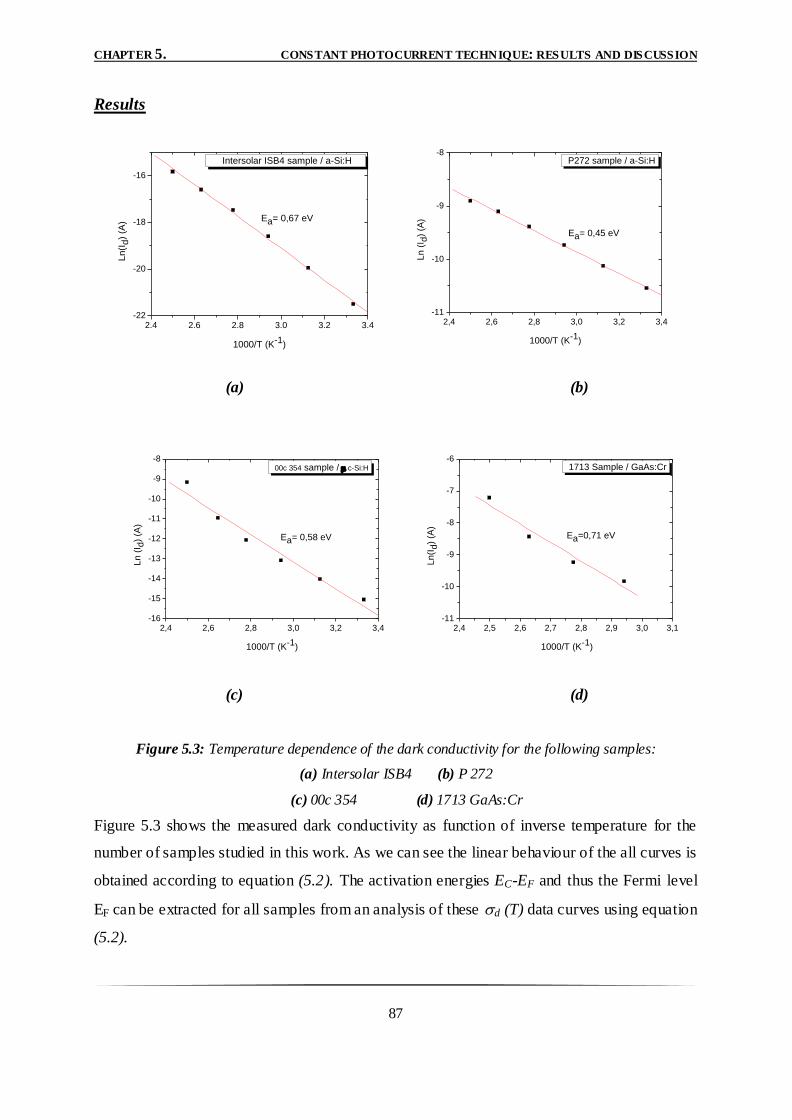
CHAPTER 5. CONSTANT PHOTOCURRENT TECHNIQUE: RESULTS AND DISCUSSION
87
Results
2.4 2.6 2.8 3.0 3.2 3.4-22
-20
-18
-16
Intersolar ISB4 sample / a-Si:H
Ea= 0,67 eV
Ln(I
d)
(A)
1000/T (K-1)
2,4 2,6 2,8 3,0 3,2 3,4-11
-10
-9
-8
P272 sample / a-Si:H
Ln (
I d)
(A)
1000/T (K-1)
Ea= 0,45 eV
(a) (b)
2,4 2,6 2,8 3,0 3,2 3,4-16
-15
-14
-13
-12
-11
-10
-9
-8
00c 354 sample / c-Si:H
Ln (
I d)
(A)
1000/T (K-1)
Ea= 0,58 eV
2,4 2,5 2,6 2,7 2,8 2,9 3,0 3,1-11
-10
-9
-8
-7
-6
1713 Sample / GaAs:Cr
Ln(I
d)
(A)
1000/T (K-1)
Ea=0,71 eV
(c) (d)
Figure 5.3: Temperature dependence of the dark conductivity for the following samples:
(a) Intersolar ISB4 (b) P 272
(c) 00c 354 (d) 1713 GaAs:Cr
Figure 5.3 shows the measured dark conductivity as function of inverse temperature for the
number of samples studied in this work. As we can see the linear behaviour of the all curves is
obtained according to equation (5.2). The activation energies EC-EF and thus the Fermi level
EF can be extracted for all samples from an analysis of these d (T) data curves using equation
(5.2).
CHAPTER 5. CONSTANT PHOTOCURRENT TECHNIQUE: RESULTS AND DISCUSSION
88
We have obtained the following results:
Sample Activation energy Ea (eV)
Intersolar ISB4 (Undoped a-Si:H)
P 272 (n-type a-Si:H)
00c 354 (c-Si:H)
1713 (GaAs:Cr)
0.67
0.45
0.58
0.71
5.4. Reflectance -Transmittance measurements
The analysis of the spectral reflectance and transmittance in the wavelength range 1, 2- 3 eV
(1035-420 nm) determines the optical parameters and the thickness of the film. The light
beam enters the film side of the film / glass structure. The solution of the Fresnel equations
for the reflectance and the transmittance of the light beam in this structure as a function of the
photon energy, h, define the refractive index, n (h), and the extinction coefficient, k (h).
The absorption coefficient, , is determined from k as 4hk/hc, where h is the Planck
constant and c is the speed of light.
The optical absorption coefficient spectrum hcan be determined in the absolute scale
(cmfrom:
The transmittance measurement by a precise matching of the relative CPM spectra in
the high absorption region to the hcalculated from the absolute transmittance
spectra Thby using the following formula [2]:
2 22 2
123 123 2 3 1 2 1 2 2
2 3
4 1 1
. ln2 1
R R T R R R R R R R
h dT R R
(5.3)
Where:
123 1 2 31 1 1R R R R
R1, R2 and R3 are the reflectance coefficients of the air- film, film-substrate and substrate-air
interfaces respectively.
CHAPTER 5. CONSTANT PHOTOCURRENT TECHNIQUE: RESULTS AND DISCUSSION
89
The absolute absorptance to transmittance ratio A/T spectra using the Ritter-Weiser
formula [20]:
2
2
2 2 21. ln 1 1 1 1 4
2
A Ah d R R R
T T
(5.4)
The optical band gap, Eg, can be found from the dependence of on h for the photon energy
region where the density of states distribution is significant. The following equation holds in
this region.
𝛼 𝑛 ℎ 𝜈 = 𝐴 ℎ 𝜈 − 𝐸𝑔 𝑝+𝑞+1
(5.5)
In this equation A is a constant and the parameters p and q are related with the shape of the
band edges. Since Tauc [23] reported a linear relation between 𝛼 𝑛 ℎ 𝜈 . and the photon
energy h, the most usual value for p and q is 1/2, corresponding to a parabolic shape of the
band edges. The band gap obtained solving equation (5.5) with these values is called the
Tauc‟s band gap, ETauc. Several authors [24, 25] have reported that a linear shape of the band
edges has better linearity than a parabolic shape of the band edges. The value for p and q
would be then equal to 1 and in this case the band gap obtained solving equation (5.5) is
called the cubic band gap. An alternative method to define the optical band gap is the energy
(Ex) at which (Ex) reaches a certain value, 10x. The band gap E 3:5 and E04 are normally
given for =10 3:5 cm-1
and =10 4 cm-1, respectively. The band gap E04 shows values ~0,2
eV higher than the Tauc band gap. This last convention has the advantage of being
independent of the shape of the band edges.
The optical absorption coefficient calculated from transmittance for all samples studied in this
thesis are shown below.
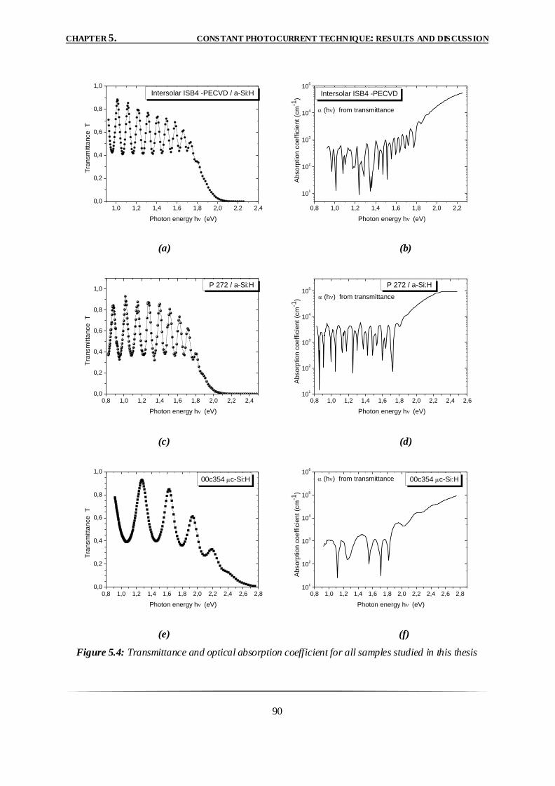
CHAPTER 5. CONSTANT PHOTOCURRENT TECHNIQUE: RESULTS AND DISCUSSION
90
1,0 1,2 1,4 1,6 1,8 2,0 2,2 2,40,0
0,2
0,4
0,6
0,8
1,0
Intersolar ISB4 -PECVD / a-Si:H
Tra
nsm
itta
nce
T
Photon energy h(eV)
0,8 1,0 1,2 1,4 1,6 1,8 2,0 2,2
101
102
103
104
105
(h) from transmittance
Intersolar ISB4 -PECVD
Absorp
tion c
oeff
icie
nt
(cm
-1)
Photon energy h(eV)
(a) (b)
0,8 1,0 1,2 1,4 1,6 1,8 2,0 2,2 2,40,0
0,2
0,4
0,6
0,8
1,0 P 272 / a-Si:H
Tra
nsm
itta
nce
T
Photon energy h(eV)
0,8 1,0 1,2 1,4 1,6 1,8 2,0 2,2 2,4 2,610
1
102
103
104
105
(h) from transmittance
P 272 / a-Si:H
Absorp
tion c
oeff
icie
nt
(cm
-1)
Photon energy h(eV)
(c) (d)
0,8 1,0 1,2 1,4 1,6 1,8 2,0 2,2 2,4 2,6 2,80,0
0,2
0,4
0,6
0,8
1,0
00c354 c-Si:H
Tra
nsm
itta
nce
T
Photon energy h(eV)
0,8 1,0 1,2 1,4 1,6 1,8 2,0 2,2 2,4 2,6 2,810
1
102
103
104
105
106
00c354 c-Si:H
Ab
so
rptio
n c
oe
ffic
ien
t (c
m-1
)
Photon energy h(eV)
(h) from transmittance
(e) (f)
Figure 5.4: Transmittance and optical absorption coefficient for all samples studied in this thesis
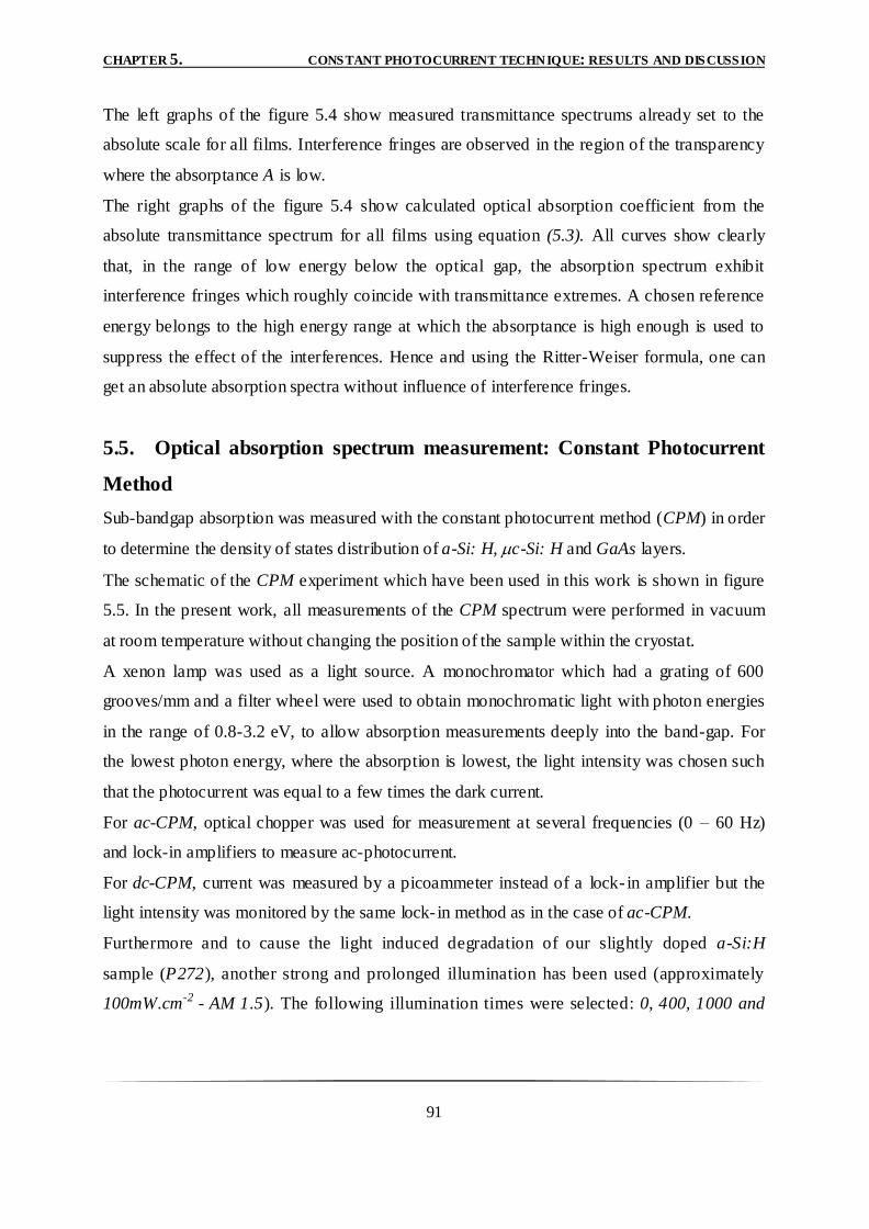
CHAPTER 5. CONSTANT PHOTOCURRENT TECHNIQUE: RESULTS AND DISCUSSION
91
The left graphs of the figure 5.4 show measured transmittance spectrums already set to the
absolute scale for all films. Interference fringes are observed in the region of the transparency
where the absorptance A is low.
The right graphs of the figure 5.4 show calculated optical absorption coefficient from the
absolute transmittance spectrum for all films using equation (5.3). All curves show clearly
that, in the range of low energy below the optical gap, the absorption spectrum exhibit
interference fringes which roughly coincide with transmittance extremes. A chosen reference
energy belongs to the high energy range at which the absorptance is high enough is used to
suppress the effect of the interferences. Hence and using the Ritter-Weiser formula, one can
get an absolute absorption spectra without influence of interference fringes.
5.5. Optical absorption spectrum measurement: Constant Photocurrent
Method
Sub-bandgap absorption was measured with the constant photocurrent method (CPM) in order
to determine the density of states distribution of a-Si: H, c-Si: H and GaAs layers.
The schematic of the CPM experiment which have been used in this work is shown in figure
5.5. In the present work, all measurements of the CPM spectrum were performed in vacuum
at room temperature without changing the position of the sample within the cryostat.
A xenon lamp was used as a light source. A monochromator which had a grating of 600
grooves/mm and a filter wheel were used to obtain monochromatic light with photon energies
in the range of 0.8-3.2 eV, to allow absorption measurements deeply into the band-gap. For
the lowest photon energy, where the absorption is lowest, the light intensity was chosen such
that the photocurrent was equal to a few times the dark current.
For ac-CPM, optical chopper was used for measurement at several frequencies (0 – 60 Hz)
and lock-in amplifiers to measure ac-photocurrent.
For dc-CPM, current was measured by a picoammeter instead of a lock- in amplifier but the
light intensity was monitored by the same lock- in method as in the case of ac-CPM.
Furthermore and to cause the light induced degradation of our slightly doped a-Si:H
sample (P272), another strong and prolonged illumination has been used (approximately
100mW.cm-2 - AM 1.5). The following illumination times were selected: 0, 400, 1000 and
CHAPTER 5. CONSTANT PHOTOCURRENT TECHNIQUE: RESULTS AND DISCUSSION
92
4000 sec in order to cover a wide range and reach the saturation point. We took CPM
spectrum after each time separately.
In the CPM, absorption coefficients, (h), are obtained as the inverse of the incident photon
number, 1/ph, under a constant photocurrent, Iph, by using conventional CPM assumptions.
The photocurrent at all energies was kept constant by controlling the intensity of the incident
light ph with a computer program. A calibrated photodiode was used to measure the photon
flux.
Absolute CPM spectra were obtained by monitoring the transmitted photon flux following the
procedures described by Vanecek et al [2]. Data were then calibrated by reference to optical
transmission measurements, through the use of the Ritter-Weiser formula [20]. The DOS was
obtained by differentiation of the absorption curve method described by Pierz et al [21].
Required instruments for this measurement:
Cryostat
HT Sample power supply
W-halogen lamp
Lamp power supply (DC power supply-PSU 35V-10A)
Optical chopper
Monochromator
Filters wheel
Beam splitter
Detectors (BPX 65)
Picoammeter ( Keithley 485)
Lock- in amplifier
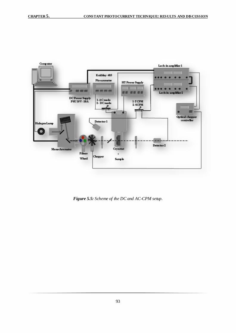
CHAPTER 5. CONSTANT PHOTOCURRENT TECHNIQUE: RESULTS AND DISCUSSION
93
Figure 5.5: Scheme of the DC and AC-CPM setup.
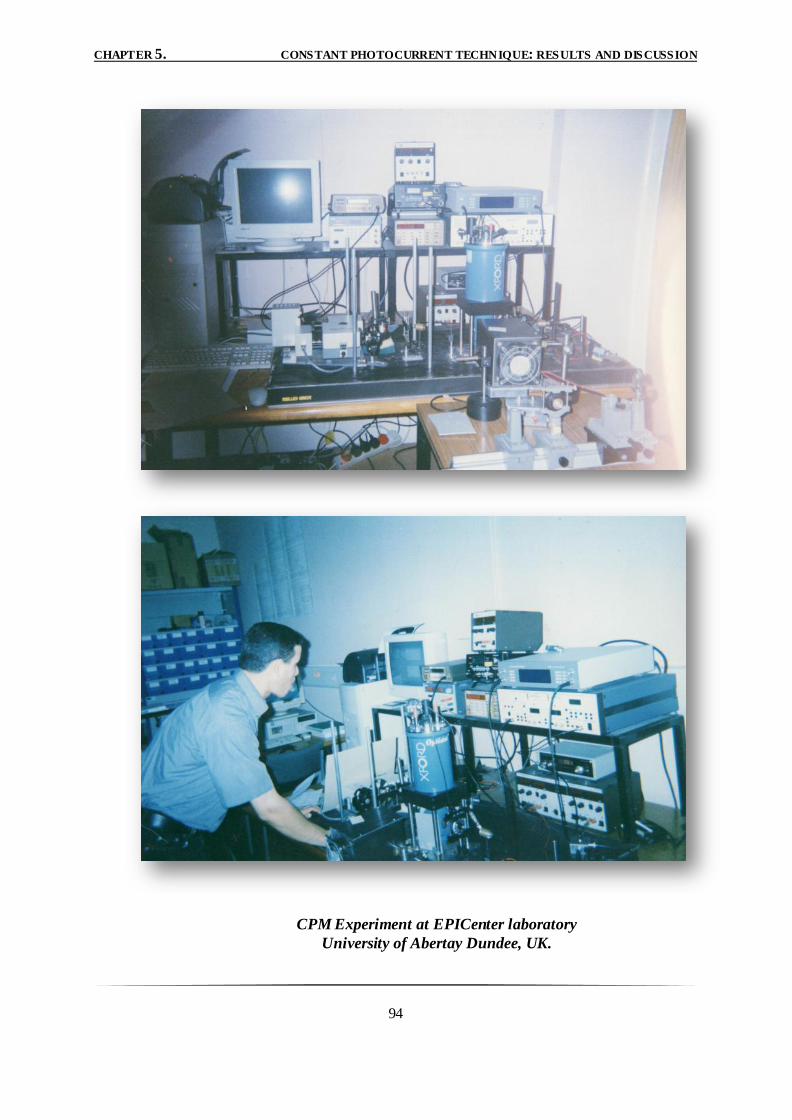
CHAPTER 5. CONSTANT PHOTOCURRENT TECHNIQUE: RESULTS AND DISCUSSION
94
CPM Experiment at EPICenter laboratory
University of Abertay Dundee, UK.
CHAPTER 5. CONSTANT PHOTOCURRENT TECHNIQUE: RESULTS AND DISCUSSION
95
5.6. Density of states
Constant photocurrent method spectra can be used to obtain information about the density of
localized gap states in a-Si:H, c-Si:H and GaAs. In fact, the absorption spectrum reflects all
the optical transitions between the electronic gap states. Consequently, this spectrum can be
converted into energy distribution of the occupied and empty localized states within the gap
by using the equation (4.45) presented in the previous chapter. Hence, four important
parameters can be deduced from the analysis of the optical absorption spectrum (h):
The Urbach energy, EU, which characterized the disorder and can be related to the
number of weak Si-Si bonds [26];
The midgap defect density, ND. There are mainly two methods that are used to get a
rapid evaluation of the defect density from CPM measurement. The first one uses the
integrated defect absorption, (- Urbach) dE, where Urbach is the contribution from the
Urbach tail; the second one uses the value of the absorption coefficient at a single
energy, typically at 1.2 eV [27]. It is thus obvious that the defect density can only be
correctly determined from a deconvolution procedure;
The energetic defect distribution within the gap states;
The charge state of the defect states.
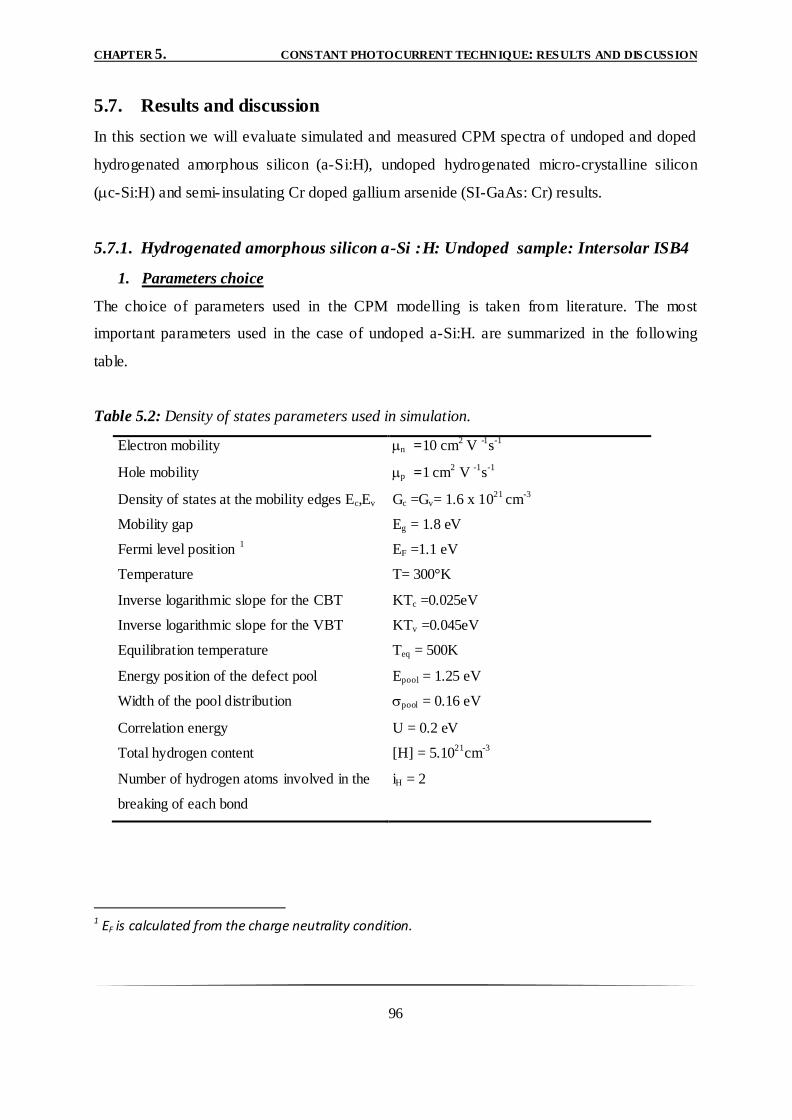
CHAPTER 5. CONSTANT PHOTOCURRENT TECHNIQUE: RESULTS AND DISCUSSION
96
5.7. Results and discussion
In this section we will evaluate simulated and measured CPM spectra of undoped and doped
hydrogenated amorphous silicon (a-Si:H), undoped hydrogenated micro-crystalline silicon
(c-Si:H) and semi- insulating Cr doped gallium arsenide (SI-GaAs: Cr) results.
5.7.1. Hydrogenated amorphous silicon a-Si :H: Undoped sample: Intersolar ISB4
1. Parameters choice
The choice of parameters used in the CPM modelling is taken from literature. The most
important parameters used in the case of undoped a-Si:H. are summarized in the following
table.
Table 5.2: Density of states parameters used in simulation.
Electron mobility n =10 cm2 V
-1s
-1
Hole mobility p =1 cm2 V
-1s
-1
Density of states at the mobility edges Ec,Ev Gc =Gv= 1.6 x 10²¹
cm-3
Mobility gap Eg = 1.8 eV
Fermi level position 1
EF =1.1 eV
Temperature T= 300°K
Inverse logarithmic slope for the CBT KTc =0.025eV
Inverse logarithmic slope for the VBT KTv =0.045eV
Equilibration temperature Teq = 500K
Energy position of the defect pool Epool = 1.25 eV
Width of the pool distribution pool = 0.16 eV
Correlation energy U = 0.2 eV
Total hydrogen content [H] = 5.1021
cm-3
Number of hydrogen atoms involved in the
breaking of each bond
iH = 2
1 EF is calculated from the charge neutrality condition.
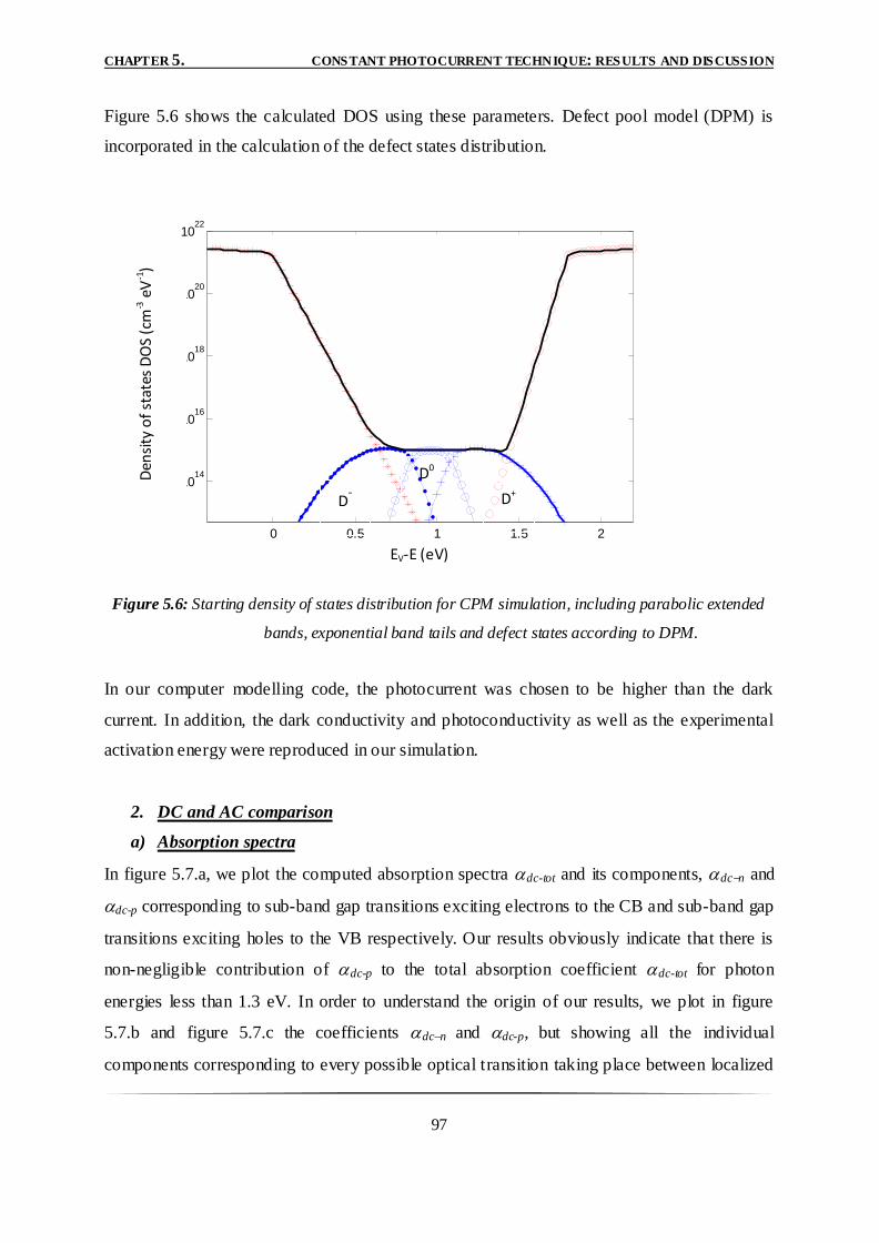
CHAPTER 5. CONSTANT PHOTOCURRENT TECHNIQUE: RESULTS AND DISCUSSION
97
0 0.5 1 1.5 2
1014
1016
1018
1020
1022
Figure 5.6 shows the calculated DOS using these parameters. Defect pool model (DPM) is
incorporated in the calculation of the defect states distribution.
Figure 5.6: Starting density of states distribution for CPM simulation, including parabolic extended
bands, exponential band tails and defect states according to DPM.
In our computer modelling code, the photocurrent was chosen to be higher than the dark
current. In addition, the dark conductivity and photoconductivity as well as the experimental
activation energy were reproduced in our simulation.
2. DC and AC comparison
a) Absorption spectra
In figure 5.7.a, we plot the computed absorption spectra dc-tot and its components, dcn and
dc-p corresponding to sub-band gap transitions exciting electrons to the CB and sub-band gap
transitions exciting holes to the VB respectively. Our results obviously indicate that there is
non-negligible contribution of dc-p to the total absorption coefficient dc-tot for photon
energies less than 1.3 eV. In order to understand the origin of our results, we plot in figure
5.7.b and figure 5.7.c the coefficients dcn and dc-p, but showing all the individual
components corresponding to every possible optical transition taking place between localized
D0
EV-E (eV)
Den
sity
of
stat
es D
OS
(cm
-3 e
V-1
)
D- D+
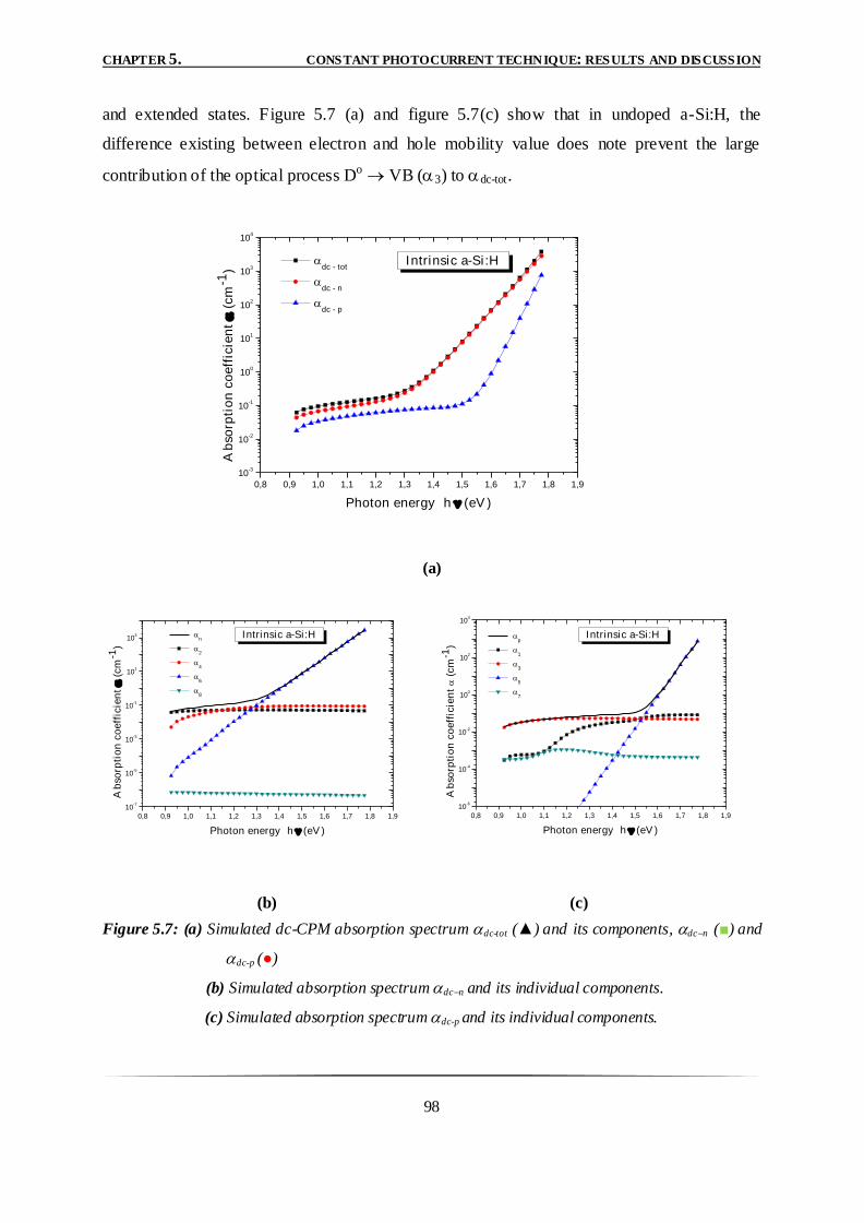
CHAPTER 5. CONSTANT PHOTOCURRENT TECHNIQUE: RESULTS AND DISCUSSION
98
and extended states. Figure 5.7 (a) and figure 5.7(c) show that in undoped a-Si:H, the
difference existing between electron and hole mobility value does note prevent the large
contribution of the optical process Do VB (3) to dc-tot.
(a)
(b) (c)
Figure 5.7: (a) Simulated dc-CPM absorption spectrum dc-tot (▲) and its components, dcn (■) and
dc-p (●)
(b) Simulated absorption spectrum dcn and its individual components.
(c) Simulated absorption spectrum dc-p and its individual components.
0,8 0,9 1,0 1,1 1,2 1,3 1,4 1,5 1,6 1,7 1,8 1,9
10-3
10-2
10-1
100
101
102
103
104
Intrinsic a-Si :H dc - tot
dc - n
dc - p
A
bso
rpti
on
co
eff
icie
nt
(cm
-1)
Photon energy h(eV )
0,8 0,9 1,0 1,1 1,2 1,3 1,4 1,5 1,6 1,7 1,8 1,9
10-7
10-5
10-3
10-1
101
103 Intrinsic a-Si :H
Ab
sorp
tio
n c
oeff
icie
nt
(cm
-1)
Photon energy h(eV )
n
2
4
6
8
0,8 0,9 1,0 1,1 1,2 1,3 1,4 1,5 1,6 1,7 1,8 1,9
10-6
10-4
10-2
100
102
104
Intrinsic a-Si :H
Ab
sorp
tio
n c
oeff
icie
nt
(cm
-1)
Photon energy h(eV )
p
1
3
5
7
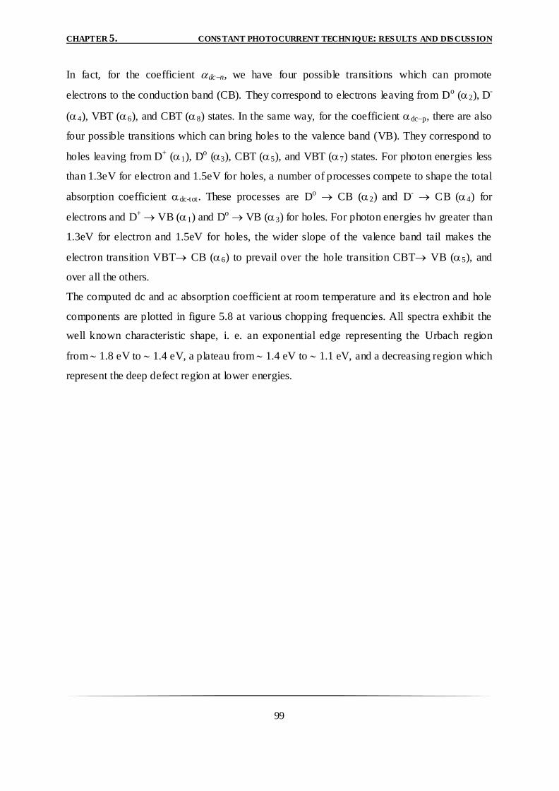
CHAPTER 5. CONSTANT PHOTOCURRENT TECHNIQUE: RESULTS AND DISCUSSION
99
In fact, for the coefficient dcn, we have four possible transitions which can promote
electrons to the conduction band (CB). They correspond to electrons leaving from Do (2), D-
(4), VBT (6), and CBT (8) states. In the same way, for the coefficient dcp, there are also
four possible transitions which can bring holes to the valence band (VB). They correspond to
holes leaving from D+ (1), Do (3), CBT (5), and VBT (7) states. For photon energies less
than 1.3eV for electron and 1.5eV for holes, a number of processes compete to shape the total
absorption coefficient dc-tot. These processes are Do CB (2) and D- CB (4) for
electrons and D+ VB (1) and Do VB (3) for holes. For photon energies h greater than
1.3eV for electron and 1.5eV for holes, the wider slope of the valence band tail makes the
electron transition VBT CB (6) to prevail over the hole transition CBT VB (5), and
over all the others.
The computed dc and ac absorption coefficient at room temperature and its electron and hole
components are plotted in figure 5.8 at various chopping frequencies. All spectra exhibit the
well known characteristic shape, i. e. an exponential edge representing the Urbach region
from 1.8 eV to 1.4 eV, a plateau from 1.4 eV to 1.1 eV, and a decreasing region which
represent the deep defect region at lower energies.
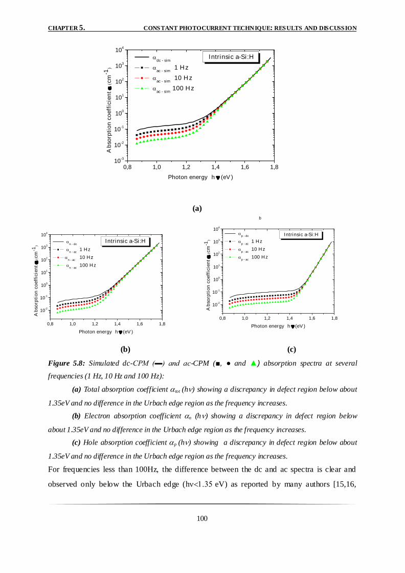
CHAPTER 5. CONSTANT PHOTOCURRENT TECHNIQUE: RESULTS AND DISCUSSION
100
(a)
(b) (c)
Figure 5.8: Simulated dc-CPM (▬) and ac-CPM (■, ● and ▲) absorption spectra at several
frequencies (1 Hz, 10 Hz and 100 Hz):
(a) Total absorption coefficient tot (h) showing a discrepancy in defect region below about
1.35eV and no difference in the Urbach edge region as the frequency increases.
(b) Electron absorption coefficient n (h) showing a discrepancy in defect region below
about 1.35eV and no difference in the Urbach edge region as the frequency increases.
(c) Hole absorption coefficient p (h) showing a discrepancy in defect region below about
1.35eV and no difference in the Urbach edge region as the frequency increases.
For frequencies less than 100Hz, the difference between the dc and ac spectra is clear and
observed only below the Urbach edge (heV) as reported by many authors [15,16,
0,8 1,0 1,2 1,4 1,6 1,810
-3
10-2
10-1
100
101
102
103
104
Ab
sorp
tio
n c
oeff
icie
nt
cm
-1
Photon energy h (eV )
dc - sim
ac - sim
1 Hz
ac - sim
10 Hz
ac - sim
100 Hz
Intrinsic a-Si :H
0,8 1,0 1,2 1,4 1,6 1,8
10-2
10-1
100
101
102
103
104
Ab
sorp
tio
n c
oeff
icie
nt
cm
-1
Photon energy h (eV )
p - dc
p - ac
1 Hz
p - ac
10 Hz
p - ac
100 Hz
Intrinsic a-Si :H
b
0,8 1,0 1,2 1,4 1,6 1,8
10-2
10-1
100
101
102
103
104
Ab
sorp
tio
n c
oeff
icie
nt
cm
-1
Photon energy h (eV )
n - dc
n - ac
1 Hz
n - ac
10 Hz
n - ac
100 Hz
Intrinsic a-Si:H
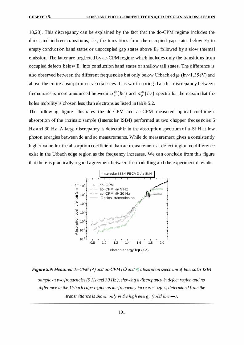
CHAPTER 5. CONSTANT PHOTOCURRENT TECHNIQUE: RESULTS AND DISCUSSION
101
18,28]. This discrepancy can be explained by the fact that the dc-CPM regime includes the
direct and indirect transitions, i.e., the transitions from the occupied gap states below EF to
empty conduction band states or unoccupied gap states above EF followed by a slow thermal
emission. The latter are neglected by ac-CPM regime which includes only the transitions from
occupied defects below EF into conduction band states or shallow tail states. The difference is
also observed between the different frequencies but only below Urbach edge (heV) and
above the entire absorption curve coalesces. It is worth noting that this discrepancy between
frequencies is more announced between dc
p h and ac
p h spectra for the reason that the
holes mobility is chosen less than electrons as listed in table 5.2.
The following figure illustrates the dc-CPM and ac-CPM measured optical coefficient
absorption of the intrinsic sample (Intersolar ISB4) performed at two chopper freque ncies 5
Hz and 30 Hz. A large discrepancy is detectable in the absorption spectrum of a-Si:H at low
photon energies between dc and ac measurements. While dc measurement gives a consistently
higher value for the absorption coefficient than ac measurement at defect region no difference
exist in the Urbach edge region as the frequency increases. We can conclude from this figure
that there is practically a good agreement between the modelling and the experimental results.
0.8 1.0 1.2 1.4 1.6 1.8 2.010
-2
10-1
100
101
102
103
104
Intersolar ISB4-PECV D / a-Si:H
Photon energy h(eV )
Ab
sorp
tio
n c
oeff
icie
nt (
cm
-1) dc- CPM
ac- CPM @ 5 Hz
ac- CPM @ 30 Hz
Optical transmission
Figure 5.9: Measured dc-CPM (△) and ac-CPM ( and ) absorption spectrum of Intersolar ISB4
sample at two frequencies (5 Hz and 30 Hz ), showing a discrepancy in defect region and no
difference in the Urbach edge region as the frequency increases.(h) determined from the
transmittance is shown only in the high energy (solid line ▬).
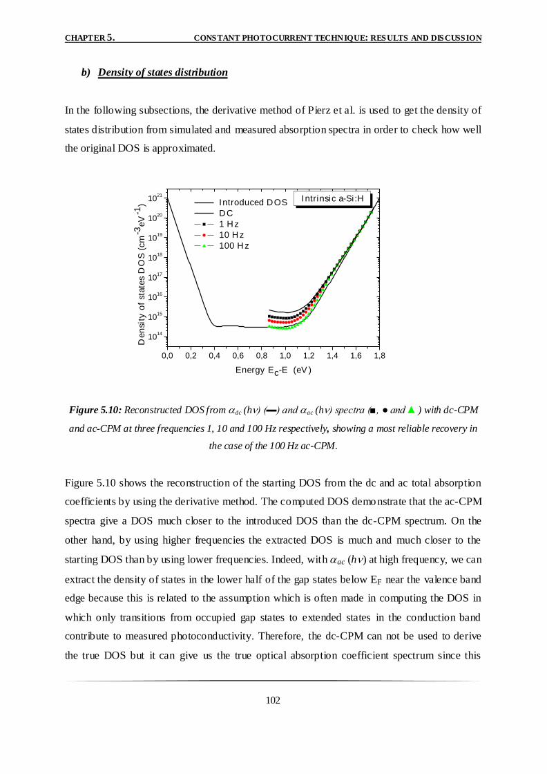
CHAPTER 5. CONSTANT PHOTOCURRENT TECHNIQUE: RESULTS AND DISCUSSION
102
b) Density of states distribution
In the following subsections, the derivative method of Pierz et al. is used to get the density of
states distribution from simulated and measured absorption spectra in order to check how well
the original DOS is approximated.
Figure 5.10: Reconstructed DOS from dc (h) (▬) and ac (h) spectra (■, ● and ▲) with dc-CPM
and ac-CPM at three frequencies 1, 10 and 100 Hz respectively, showing a most reliable recovery in
the case of the 100 Hz ac-CPM.
Figure 5.10 shows the reconstruction of the starting DOS from the dc and ac total absorption
coefficients by using the derivative method. The computed DOS demonstrate that the ac-CPM
spectra give a DOS much closer to the introduced DOS than the dc-CPM spectrum. On the
other hand, by using higher frequencies the extracted DOS is much and much closer to the
starting DOS than by using lower frequencies. Indeed, with ac (h) at high frequency, we can
extract the density of states in the lower half of the gap states below EF near the valence band
edge because this is related to the assumption which is often made in computing the DOS in
which only transitions from occupied gap states to extended states in the conduction band
contribute to measured photoconductivity. Therefore, the dc-CPM can not be used to derive
the true DOS but it can give us the true optical absorption coefficient spectrum since this
0,0 0,2 0,4 0,6 0,8 1,0 1,2 1,4 1,6 1,8
1014
1015
1016
1017
1018
1019
1020
1021
Den
sity
of
state
s D
OS
(cm
-3eV
-1)
Energy Ec-E (eV )
Introduced DOS
DC
1 Hz
10 Hz
100 Hz
Intrinsic a-Si :H
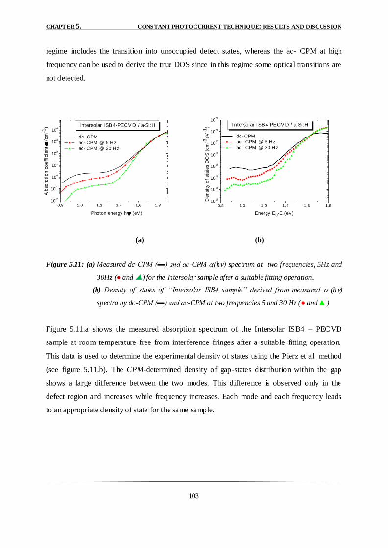
CHAPTER 5. CONSTANT PHOTOCURRENT TECHNIQUE: RESULTS AND DISCUSSION
103
regime includes the transition into unoccupied defect states, whereas the ac- CPM at high
frequency can be used to derive the true DOS since in this regime some optical transitions are
not detected.
(a) (b)
Figure 5.11: (a) Measured dc-CPM (▬) and ac-CPM (h) spectrum at two frequencies, 5Hz and
30Hz (● and ) for the Intersolar sample after a suitable fitting operation.
(b) Density of states of ‘‘Intersolar ISB4 sample’’ derived from measured (h)
spectra by dc-CPM (▬) and ac-CPM at two frequencies 5 and 30 Hz (● and ▲)
Figure 5.11.a shows the measured absorption spectrum of the Intersolar ISB4 – PECVD
sample at room temperature free from interference fringes after a suitable fitting operation.
This data is used to determine the experimental density of states using the Pierz et al. method
(see figure 5.11.b). The CPM-determined density of gap-states distribution within the gap
shows a large difference between the two modes. This difference is observed only in the
defect region and increases while frequency increases. Each mode and each frequency leads
to an appropriate density of state for the same sample.
0,8 1,0 1,2 1,4 1,6 1,810
15
1016
1017
1018
1019
1020
1021
1022
Intersolar ISB4-PECV D / a-Si:H
Den
sity
of
state
s D
OS
(cm
-3eV
-1)
Energy Ec-E (eV )
dc- CPM
ac - CPM @ 5 Hz
ac - CPM @ 30 Hz
0,8 1,0 1,2 1,4 1,6 1,810
-2
10-1
100
101
102
103
104
Intersolar ISB4-PECV D / a-Si:H
Photon energy h(eV )
Ab
sorp
tio
n c
oeff
icie
nt
(cm
-1)
dc- CPM
ac- CPM @ 5 Hz
ac- CPM @ 30 Hz
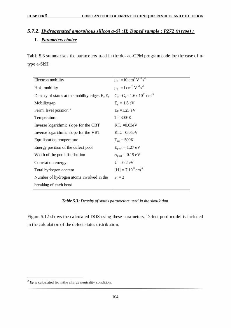
CHAPTER 5. CONSTANT PHOTOCURRENT TECHNIQUE: RESULTS AND DISCUSSION
104
5.7.2. Hydrogenated amorphous silicon a-Si :H: Doped sample : P272 (n type) :
1. Parameters choice
Table 5.3 summarizes the parameters used in the dc- ac-CPM program code for the case of n-
type a-Si:H.
Electron mobility n =10 cm2 V
-1s
-1
Hole mobility p =1 cm2 V
-1s
-1
Density of states at the mobility edges Ec,Ev Gc =Gv= 1.6x 10²¹
cm-3
Mobilitygap Eg = 1.8 eV
Fermi level position 2
EF =1.25 eV
Temperature T= 300°K
Inverse logarithmic slope for the CBT KTc =0.03eV
Inverse logarithmic slope for the VBT KTv =0.05eV
Equilibration temperature Teq = 500K
Energy position of the defect pool Epool = 1.27 eV
Width of the pool distribution pool = 0.19 eV
Correlation energy U = 0.2 eV
Total hydrogen content [H] = 7.1021
cm-3
Number of hydrogen atoms involved in the
breaking of each bond
iH = 2
Table 5.3: Density of states parameters used in the simulation.
Figure 5.12 shows the calculated DOS using these parameters. Defect pool model is included
in the calculation of the defect states distribution.
2 EF is calculated from the charge neutrality condition.
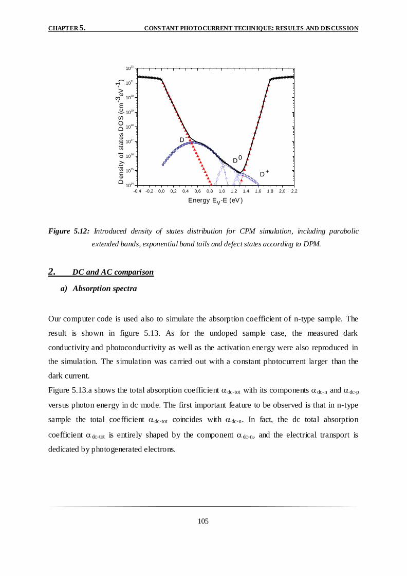
CHAPTER 5. CONSTANT PHOTOCURRENT TECHNIQUE: RESULTS AND DISCUSSION
105
-0,4 -0,2 0,0 0,2 0,4 0,6 0,8 1,0 1,2 1,4 1,6 1,8 2,0 2,2
1014
1015
1016
1017
1018
1019
1020
1021
1022
D0
D -
Den
sity
of
state
s D
OS
(cm
-3eV
-1)
Energy Ev-E (eV )
D+
Figure 5.12: Introduced density of states distribution for CPM simulation, including parabolic
extended bands, exponential band tails and defect states according to DPM.
2. DC and AC comparison
a) Absorption spectra
Our computer code is used also to simulate the absorption coefficient of n-type sample. The
result is shown in figure 5.13. As for the undoped sample case, the measured dark
conductivity and photoconductivity as well as the activation energy were also reproduced in
the simulation. The simulation was carried out with a constant photocurrent larger than the
dark current.
Figure 5.13.a shows the total absorption coefficient dc-tot with its components dc-n and dc-p
versus photon energy in dc mode. The first important feature to be observed is that in n-type
sample the total coefficient dc-tot coincides with dc-n. In fact, the dc total absorption
coefficient dc-tot is entirely shaped by the component dc-n, and the electrical transport is
dedicated by photogenerated electrons.
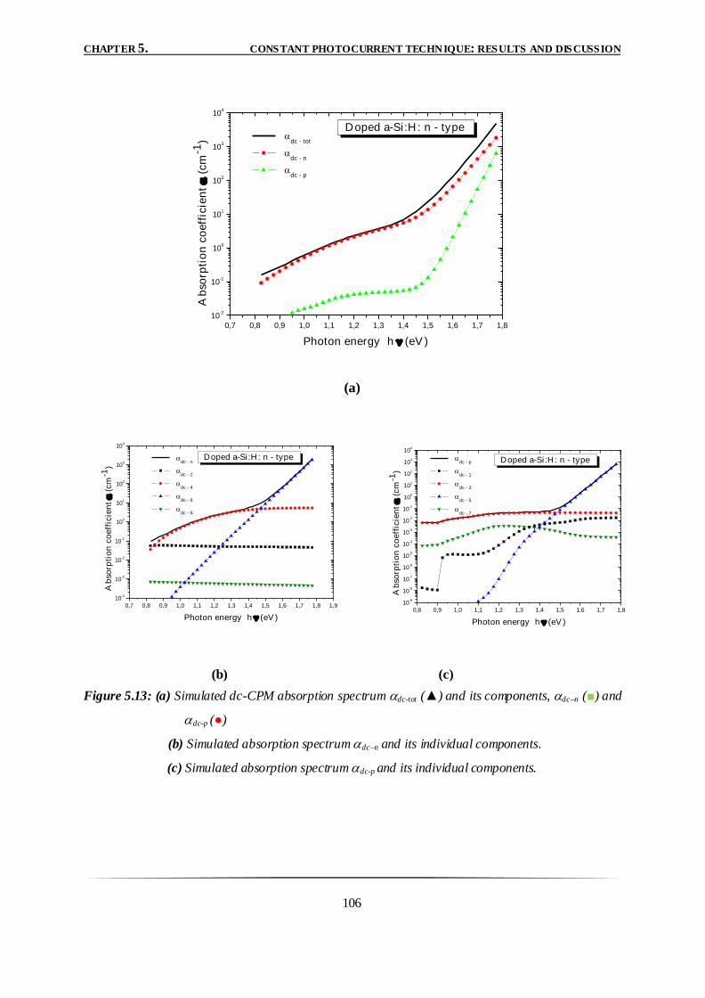
CHAPTER 5. CONSTANT PHOTOCURRENT TECHNIQUE: RESULTS AND DISCUSSION
106
(a)
(b) (c)
Figure 5.13: (a) Simulated dc-CPM absorption spectrum dc-tot (▲) and its components, dcn (■) and
dc-p (●)
(b) Simulated absorption spectrum dcn and its individual components.
(c) Simulated absorption spectrum dc-p and its individual components.
0,8 0,9 1,0 1,1 1,2 1,3 1,4 1,5 1,6 1,7 1,8
10-9
10-8
10-7
10-6
10-5
10-4
10-3
10-2
10-1
100
101
102
103
104
Doped a-Si :H : n - type
Ab
sorp
tio
n c
oeff
icie
nt
(cm
-1)
Photon energy h(eV )
dc - p
dc - 1
dc - 3
dc - 5
dc - 7
0,7 0,8 0,9 1,0 1,1 1,2 1,3 1,4 1,5 1,6 1,7 1,8 1,9
10-4
10-3
10-2
10-1
100
101
102
103
104
Doped a-Si :H : n - type
Ab
sorp
tio
n c
oeff
icie
nt
(cm
-1)
Photon energy h(eV )
dc - n
dc - 2
dc - 4
dc - 6
dc - 8
0,7 0,8 0,9 1,0 1,1 1,2 1,3 1,4 1,5 1,6 1,7 1,8
10-2
10-1
100
101
102
103
104
Doped a-Si :H : n - type
Ab
sorp
tio
n c
oeff
icie
nt
(cm
-1)
Photon energy h(eV )
dc - tot
dc - n
dc - p
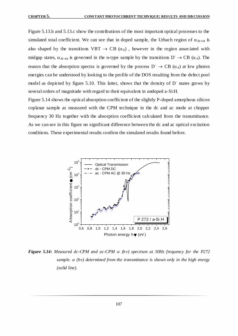
CHAPTER 5. CONSTANT PHOTOCURRENT TECHNIQUE: RESULTS AND DISCUSSION
107
Figure 5.13.b and 5.13.c show the contributions of the most important optical processes to the
simulated total coefficient. We can see that in doped sample, the Urbach region of dc-tot is
also shaped by the transitions VBT CB (6) , however in the region associated with
midgap states, dc-tot is governed in the n-type sample by the transitions D- CB (4). The
reason that the absorption spectra is governed by the process D- CB (4) at low photon
energies can be understood by looking to the profile of the DOS resulting from the defect pool
model as depicted by figure 5.10. This latter, shows that the density of D- states grows by
several orders of magnitude with regard to their equivalent in undoped a-Si:H.
Figure 5.14 shows the optical absorption coefficient of the slightly P-doped amorphous silicon
coplanar sample as measured with the CPM technique in the dc and ac mode at chopper
frequency 30 Hz together with the absorption coefficient calculated from the transmittance.
As we can see in this figure no significant difference between the dc and ac optical excitation
conditions. These experimental results confirm the simulated results found before.
0,6 0,8 1,0 1,2 1,4 1,6 1,8 2,0 2,2 2,4 2,610
0
101
102
103
104
105
P 272 / a-Si:H
Ab
sorp
tio
n c
oeff
icie
nt
(cm
-1)
Photon energy h(eV )
Optical Transmission
dc - CPM DC
ac - CPM AC @ 30 Hz
Figure 5.14: Measured dc-CPM and ac-CPM (h) spectrum at 30Hz frequency for the P272
sample. (h) determined from the transmittance is shown only in the high energy
(solid line).
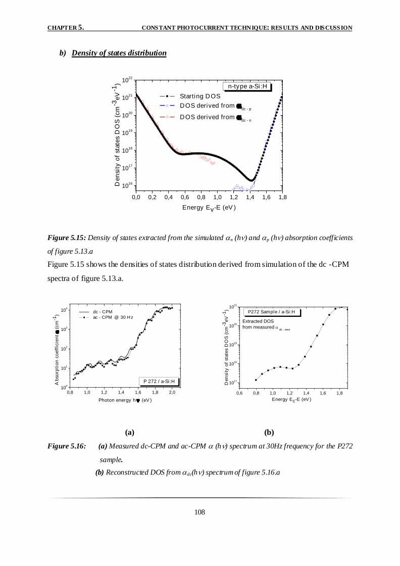
CHAPTER 5. CONSTANT PHOTOCURRENT TECHNIQUE: RESULTS AND DISCUSSION
108
b) Density of states distribution
0,0 0,2 0,4 0,6 0,8 1,0 1,2 1,4 1,6 1,8
1016
1017
1018
1019
1020
1021
1022
n-type a-Si :H
Den
sity
of
state
s D
OS
(cm
-3eV
-1)
Energy Ev-E (eV )
Starting DOS
DOS derived from dc - p
DOS derived from dc - n
Figure 5.15: Density of states extracted from the simulated n (h) and p (h) absorption coefficients
of figure 5.13.a
Figure 5.15 shows the densities of states distribution derived from simulation of the dc -CPM
spectra of figure 5.13.a.
(a) (b)
Figure 5.16: (a) Measured dc-CPM and ac-CPM (h) spectrum at 30Hz frequency for the P272
sample.
(b) Reconstructed DOS from dc(h) spectrum of figure 5.16.a
0,6 0,8 1,0 1,2 1,4 1,6 1,8
1017
1018
1019
1020
1021
P272 Sample / a-Si :H
Den
sity
of
state
s D
OS
(cm
-3eV
-1)
Energy Ec-E (eV )
Extracted DOS
from measured dc - mes
0,8 1,0 1,2 1,4 1,6 1,8 2,010
0
101
102
103
104
P 272 / a-Si:H
Ab
sorp
tio
n c
oeff
icie
nt
(cm
-1)
Photon energy h (eV )
dc - CPM
ac - CPM @ 30 Hz
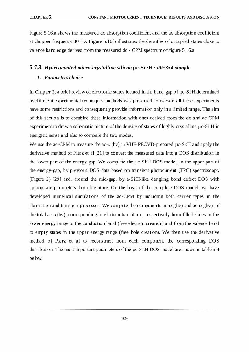
CHAPTER 5. CONSTANT PHOTOCURRENT TECHNIQUE: RESULTS AND DISCUSSION
109
Figure 5.16.a shows the measured dc absorption coefficient and the ac absorption coefficient
at chopper frequency 30 Hz. Figure 5.16.b illustrates the densities of occupied states close to
valence band edge derived from the measured dc - CPM spectrum of figure 5.16.a.
5.7.3. Hydrogenated micro-crystalline silicon c-Si :H : 00c354 sample
1. Parameters choice
In Chapter 2, a brief review of electronic states located in the band gap of μc-Si:H determined
by different experimental techniques methods was presented. However, all these experiments
have some restrictions and consequently provide information only in a limited range. The aim
of this section is to combine these information with ones derived from the dc a nd ac CPM
experiment to draw a schematic picture of the density of states of highly crystalline μc-Si:H in
energetic sense and also to compare the two modes.
We use the ac-CPM to measure the ac-(h) in VHF-PECVD-prepared µc-Si:H and apply the
derivative method of Pierz et al [21] to convert the measured data into a DOS distribution in
the lower part of the energy-gap. We complete the µc-Si:H DOS model, in the upper part of
the energy-gap, by previous DOS data based on transient photocurrent (TPC) spectroscopy
(Figure 2) [29] and, around the mid-gap, by a-Si:H-like dangling bond defect DOS with
appropriate parameters from literature. On the basis of the complete DOS model, we have
developed numerical simulations of the ac-CPM by including both carrier types in the
absorption and transport processes. We compute the components ac-n(h) and ac-p(h), of
the total ac-(h), corresponding to electron transitions, respectively from filled states in the
lower energy range to the conduction band (free electron creation) and from the valence band
to empty states in the upper energy range (free hole creation). We then use the der ivative
method of Pierz et al to reconstruct from each component the corresponding DOS
distribution. The most important parameters of the µc-Si:H DOS model are shown in table 5.4
below.
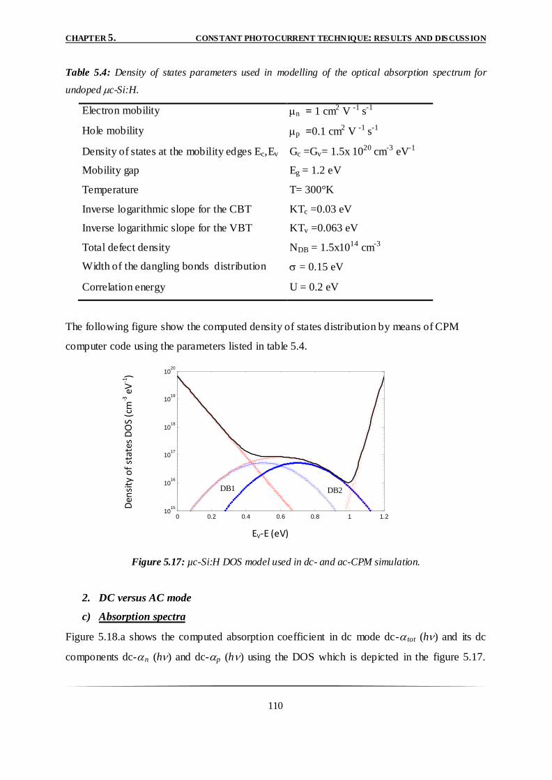
CHAPTER 5. CONSTANT PHOTOCURRENT TECHNIQUE: RESULTS AND DISCUSSION
110
Table 5.4: Density of states parameters used in modelling of the optical absorption spectrum for
undoped c-Si:H.
Electron mobility n = 1 cm2 V -1 s-1
Hole mobility p =0.1 cm2 V -1 s-1
Density of states at the mobility edges Ec,Ev Gc =Gv= 1.5x 1020 cm-3 eV-1
Mobility gap Eg = 1.2 eV
Temperature T= 300°K
Inverse logarithmic slope for the CBT KTc =0.03 eV
Inverse logarithmic slope for the VBT KTv =0.063 eV
Total defect density NDB = 1.5x1014 cm-3
Width of the dangling bonds distribution = 0.15 eV
Correlation energy U = 0.2 eV
The following figure show the computed density of states distribution by means of CPM
computer code using the parameters listed in table 5.4.
Figure 5.17: µc-Si:H DOS model used in dc- and ac-CPM simulation.
2. DC versus AC mode
c) Absorption spectra
Figure 5.18.a shows the computed absorption coefficient in dc mode dc-tot (h) and its dc
components dc-n (h) and dc-p (h) using the DOS which is depicted in the figure 5.17.
0 0.2 0.4 0.6 0.8 1 1.210
15
1016
1017
1018
1019
1020
DB1 DB2
EV-E (eV)
Den
sity
of
stat
es D
OS
(cm
-3 e
V-1
)
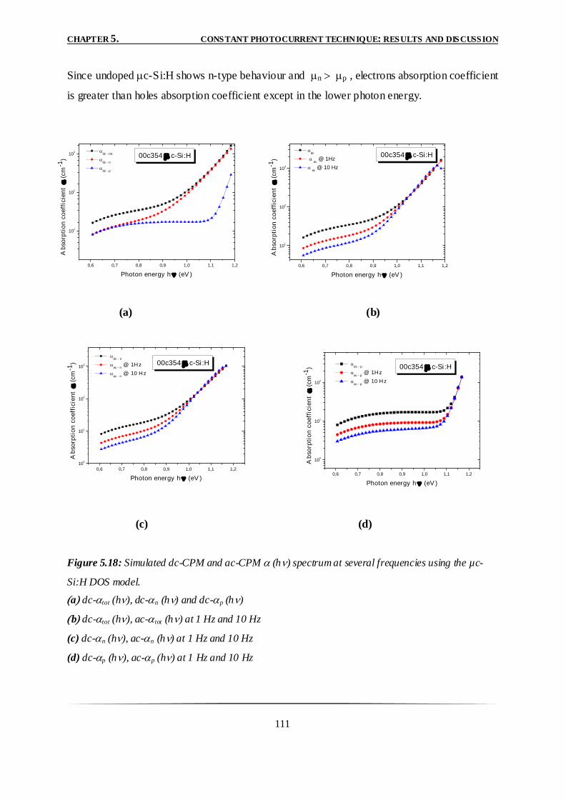
CHAPTER 5. CONSTANT PHOTOCURRENT TECHNIQUE: RESULTS AND DISCUSSION
111
Since undoped c-Si:H shows n-type behaviour and np , electrons absorption coefficient
is greater than holes absorption coefficient except in the lower photon energy.
(a) (b)
(c) (d)
Figure 5.18: Simulated dc-CPM and ac-CPM (h) spectrum at several frequencies using the µc-
Si:H DOS model.
adc-tot (h), dc-n (h) and dc-p (h)
b dc-tot (h), ac-tot (h) at 1 Hz and 10 Hz
(c) dc-n (h), ac-n (h) at 1 Hz and 10 Hz
(d) dc-p (h), ac-p (h) at 1 Hz and 10 Hz
0,6 0,7 0,8 0,9 1,0 1,1 1,2
101
102
103
00c354 c-Si:H
Ab
sorp
tio
n c
oeff
icie
nt
(
cm
-1)
Photon energy h(eV )
dc
ac
@ 1Hz
ac
@ 10 Hz
0,6 0,7 0,8 0,9 1,0 1,1 1,2
101
102
103
00c354 c-Si:H
Ab
sorp
tio
n c
oeff
icie
nt
(
cm
-1)
Photon energy h(eV )
dc - tot
dc - n
dc - p
0,6 0,7 0,8 0,9 1,0 1,1 1,2
100
101
102
103
dc - n
ac - n
@ 1Hz
ac - n
@ 10 Hz
00c354 c-Si:H
Ab
sorp
tio
n c
oeff
icie
nt
(
cm
-1)
Photon energy h(eV )0,6 0,7 0,8 0,9 1,0 1,1 1,2
100
101
102
00c354 c-Si:H
Ab
sorp
tio
n c
oeff
icie
nt
(
cm
-1)
Photon energy h(eV )
dc - p
ac - p
@ 1Hz
ac - p
@ 10 Hz
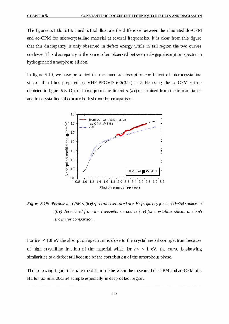
CHAPTER 5. CONSTANT PHOTOCURRENT TECHNIQUE: RESULTS AND DISCUSSION
112
The figures 5.18.b, 5.18. c and 5.18.d illustrate the difference between the simulated dc-CPM
and ac-CPM for microcrystalline material at several frequencies. It is clear from this figure
that this discrepancy is only observed in defect energy while in tail region the two curves
coalesce. This discrepancy is the same often observed between sub-gap absorption spectra in
hydrogenated amorphous silicon.
In figure 5.19, we have presented the measured ac absorption coefficient of microcrystalline
silicon thin films prepared by VHF PECVD (00c354) at 5 Hz using the ac-CPM set up
depicted in figure 5.5. Optical absorption coefficient (h) determined from the transmittance
and for crystalline silicon are both shown for comparison.
0,8 1,0 1,2 1,4 1,6 1,8 2,0 2,2 2,4 2,6 2,8 3,0 3,210
-1
100
101
102
103
104
105
106
00c354 c-Si:H
Ab
sorp
tio
n c
oeff
icie
nt
(
cm
-1)
Photon energy h(eV )
from optical transmission
ac-CPM @ 5Hz
c-Si
Figure 5.19: Absolute ac-CPM (h) spectrum measured at 5 Hz frequency for the 00c354 sample.
(h) determined from the transmittance and (h) for crystalline silicon are both
shown for comparison.
For h < 1.8 eV the absorption spectrum is close to the crystalline silicon spectrum because
of high crystalline fraction of the material while for h < 1 eV, the curve is showing
similarities to a defect tail because of the contribution of the amorphous phase.
The following figure illustrate the difference between the measured dc-CPM and ac-CPM at 5
Hz for µc-Si:H 00c354 sample especially in deep defect region.
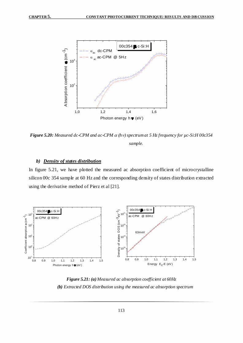
CHAPTER 5. CONSTANT PHOTOCURRENT TECHNIQUE: RESULTS AND DISCUSSION
113
Figure 5.20: Measured dc-CPM and ac-CPM (h) spectrum at 5 Hz frequency for µc-Si:H 00c354
sample.
b) Density of states distribution
In figure 5.21, we have plotted the measured ac absorption coefficient of microcrystalline
silicon 00c 354 sample at 60 Hz and the corresponding density of states distribution extracted
using the derivative method of Pierz et al [21].
Figure 5.21: (a) Measured ac absorption coefficient at 60Hz
(b) Extracted DOS distribution using the measured ac absorption spectrum
1,0 1,2 1,4 1,6
102
103
00c354 c-Si :H
Ab
sorp
tio
n c
oeff
icie
nt
(
cm
-1)
Photon energy h (eV )
dc
dc-CPM
ac
ac-CPM @ 5Hz
0,8 0,9 1,0 1,1 1,2 1,3 1,4 1,510
-1
100
101
102
103
00c354 c-Si :H
Co
eff
icie
nt
ab
sorp
tio
n a
(cm
-1)
Photon energy h (eV )
ac-CPM @ 60Hz
0,8 0,9 1,0 1,1 1,2 1,3 1,4 1,5
1018
1019
1020
1021
63meV
00c354 c-Si :H
ac-CPM @ 60Hz
Den
sity
of
state
s D
OS
(cm
-3eV
-1)
Energy Ec-E (eV )
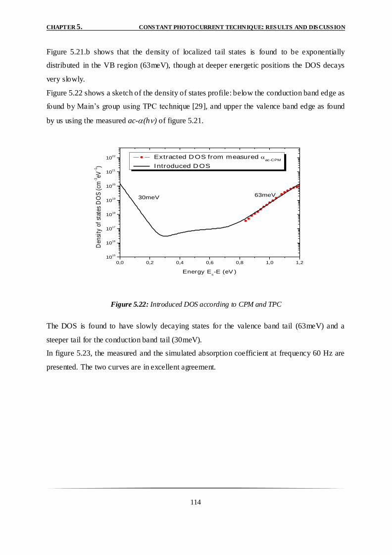
CHAPTER 5. CONSTANT PHOTOCURRENT TECHNIQUE: RESULTS AND DISCUSSION
114
Figure 5.21.b shows that the density of localized tail states is found to be exponentially
distributed in the VB region (63meV), though at deeper energetic positions the DOS decays
very slowly.
Figure 5.22 shows a sketch of the density of states profile: below the conduction band edge as
found by Main‟s group using TPC technique [29], and upper the valence band edge as found
by us using the measured ac-(h) of figure 5.21.
0,0 0,2 0,4 0,6 0,8 1,0 1,2
1015
1016
1017
1018
1019
1020
1021
1022
Den
sity
of
stat
es D
OS
(cm
-3eV
-1)
Energy Ec-E (eV )
Extracted DOS from measured ac-CPM
Introduced DOS
63meV30meV
Figure 5.22: Introduced DOS according to CPM and TPC
The DOS is found to have slowly decaying states for the valence band tail (63meV) and a
steeper tail for the conduction band tail (30meV).
In figure 5.23, the measured and the simulated absorption coefficient at frequency 60 Hz are
presented. The two curves are in excellent agreement.
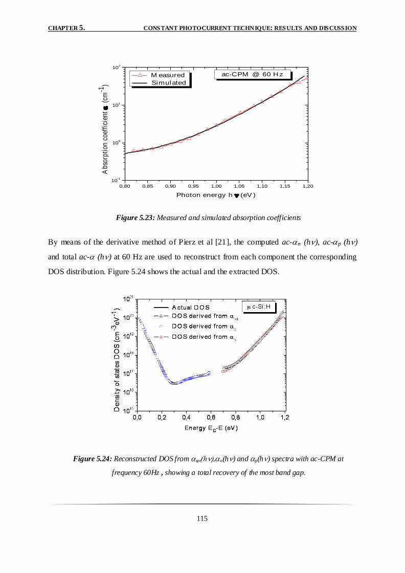
CHAPTER 5. CONSTANT PHOTOCURRENT TECHNIQUE: RESULTS AND DISCUSSION
115
0,80 0,85 0,90 0,95 1,00 1,05 1,10 1,15 1,20
10-1
100
101
102
Ab
sorp
tio
n c
oef
fici
ent (
cm-1
)
Photon energy h (eV )
M easured
Simulated
ac-CPM @ 60 H z
Figure 5.23: Measured and simulated absorption coefficients
By means of the derivative method of Pierz et al [21], the computed ac-n (h), ac-p (h)
and total ac- (h) at 60 Hz are used to reconstruct from each component the corresponding
DOS distribution. Figure 5.24 shows the actual and the extracted DOS.
Figure 5.24: Reconstructed DOS from tot(h),n(h) and p(h) spectra with ac-CPM at
frequency 60Hz , showing a total recovery of the most band gap.
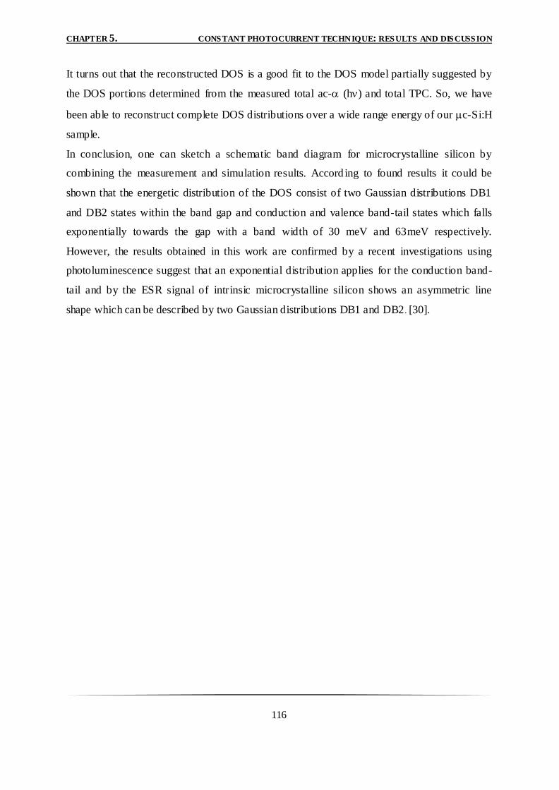
CHAPTER 5. CONSTANT PHOTOCURRENT TECHNIQUE: RESULTS AND DISCUSSION
116
It turns out that the reconstructed DOS is a good fit to the DOS model partially suggested by
the DOS portions determined from the measured total ac- (h) and total TPC. So, we have
been able to reconstruct complete DOS distributions over a wide range energy of our c-Si:H
sample.
In conclusion, one can sketch a schematic band diagram for microcrystalline silicon by
combining the measurement and simulation results. Accord ing to found results it could be
shown that the energetic distribution of the DOS consist of two Gaussian distributions DB1
and DB2 states within the band gap and conduction and valence band-tail states which falls
exponentially towards the gap with a band width of 30 meV and 63meV respectively.
However, the results obtained in this work are confirmed by a recent investigations using
photoluminescence suggest that an exponential distribution applies for the conduction band-
tail and by the ESR signal of intrinsic microcrystalline silicon shows an asymmetric line
shape which can be described by two Gaussian distributions DB1 and DB2 . [30].
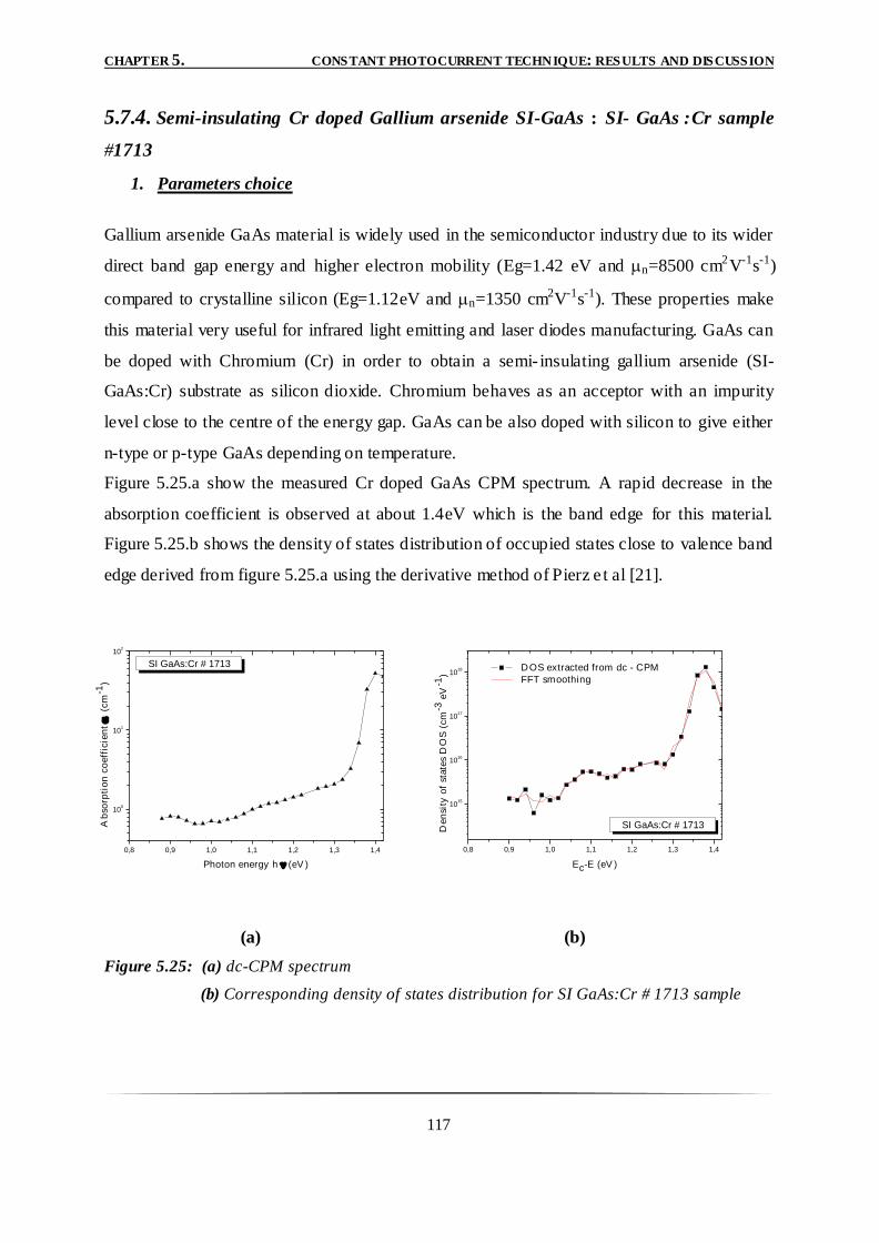
CHAPTER 5. CONSTANT PHOTOCURRENT TECHNIQUE: RESULTS AND DISCUSSION
117
5.7.4. Semi-insulating Cr doped Gallium arsenide SI-GaAs : SI- GaAs :Cr sample
#1713
1. Parameters choice
Gallium arsenide GaAs material is widely used in the semiconductor industry due to its wider
direct band gap energy and higher electron mobility (Eg=1.42 eV and n=8500 cm2V-1s-1)
compared to crystalline silicon (Eg=1.12eV and n=1350 cm2V-1s-1). These properties make
this material very useful for infrared light emitting and laser diodes manufacturing. GaAs can
be doped with Chromium (Cr) in order to obtain a semi- insulating gallium arsenide (SI-
GaAs:Cr) substrate as silicon dioxide. Chromium behaves as an acceptor with an impurity
level close to the centre of the energy gap. GaAs can be also doped with silicon to give either
n-type or p-type GaAs depending on temperature.
Figure 5.25.a show the measured Cr doped GaAs CPM spectrum. A rapid decrease in the
absorption coefficient is observed at about 1.4eV which is the band edge for this material.
Figure 5.25.b shows the density of states distribution of occupied states close to valence band
edge derived from figure 5.25.a using the derivative method of Pierz e t al [21].
(a) (b)
Figure 5.25: (a) dc-CPM spectrum
(b) Corresponding density of states distribution for SI GaAs:Cr # 1713 sample
0,8 0,9 1,0 1,1 1,2 1,3 1,4
100
101
102
SI GaAs:Cr # 1713
Ab
sorp
tio
n c
oeff
icie
nt (c
m-1
)
Photon energy h (eV )
0,8 0,9 1,0 1,1 1,2 1,3 1,4
1015
1016
1017
1018
SI GaAs:Cr # 1713
Den
sity
of
state
s D
OS
(cm
-3 e
V-1
)
Ec-E (eV )
DOS extracted from dc - CPM
FFT smoothing
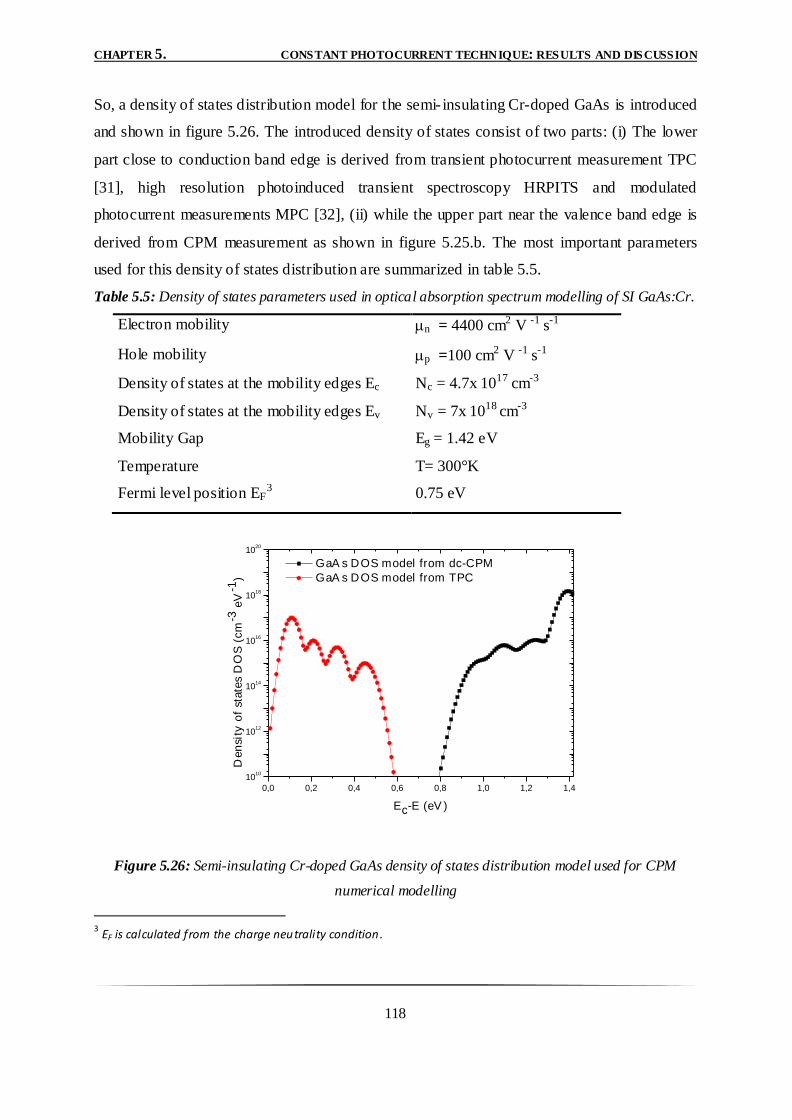
CHAPTER 5. CONSTANT PHOTOCURRENT TECHNIQUE: RESULTS AND DISCUSSION
118
So, a density of states distribution model for the semi- insulating Cr-doped GaAs is introduced
and shown in figure 5.26. The introduced density of states consist of two parts: (i) The lower
part close to conduction band edge is derived from transient photocurrent measurement TPC
[31], high resolution photoinduced transient spectroscopy HRPITS and modulated
photocurrent measurements MPC [32], (ii) while the upper part near the valence band edge is
derived from CPM measurement as shown in figure 5.25.b. The most important parameters
used for this density of states distribution are summarized in table 5.5.
Table 5.5: Density of states parameters used in optical absorption spectrum modelling of SI GaAs:Cr.
Electron mobility n = 4400 cm2 V -1 s-1
Hole mobility p =100 cm2 V -1 s-1
Density of states at the mobility edges Ec Nc = 4.7x 1017 cm-3
Density of states at the mobility edges Ev Nv = 7x 1018 cm-3
Mobility Gap Eg = 1.42 eV
Temperature T= 300°K
Fermi level position EF3 0.75 eV
0,0 0,2 0,4 0,6 0,8 1,0 1,2 1,4
1010
1012
1014
1016
1018
1020
Den
sity
of
state
s D
OS
(cm
-3 e
V-1
)
Ec-E (eV )
GaA s DOS model from dc-CPM
GaA s DOS model from TPC
Figure 5.26: Semi-insulating Cr-doped GaAs density of states distribution model used for CPM
numerical modelling
3 EF is calculated from the charge neutrality condition.
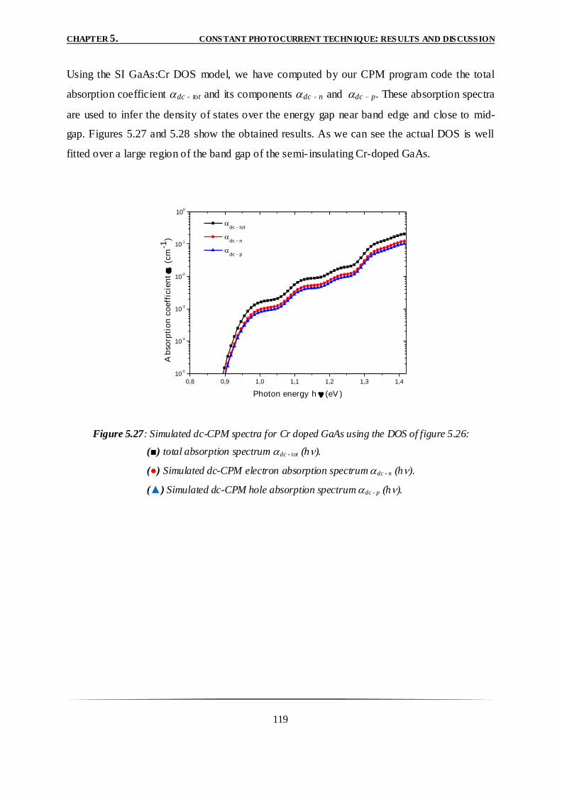
CHAPTER 5. CONSTANT PHOTOCURRENT TECHNIQUE: RESULTS AND DISCUSSION
119
Using the SI GaAs:Cr DOS model, we have computed by our CPM program code the total
absorption coefficient dc - tot and its components dc - n anddc – p. These absorption spectra
are used to infer the density of states over the energy gap near band edge and close to mid-
gap. Figures 5.27 and 5.28 show the obtained results. As we can see the actual DOS is well
fitted over a large region of the band gap of the semi- insulating Cr-doped GaAs.
0,8 0,9 1,0 1,1 1,2 1,3 1,4
10-5
10-4
10-3
10-2
10-1
100
Ab
sorp
tio
n c
oeff
icie
nt (c
m-1
)
Photon energy h (eV )
dc - tot
dc - n
dc - p
Figure 5.27: Simulated dc-CPM spectra for Cr doped GaAs using the DOS of figure 5.26:
(■) total absorption spectrum dc - tot (h).
(●) Simulated dc-CPM electron absorption spectrum dc - n (h).
(▲) Simulated dc-CPM hole absorption spectrum dc - p (h).
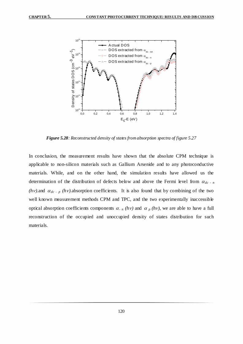
CHAPTER 5. CONSTANT PHOTOCURRENT TECHNIQUE: RESULTS AND DISCUSSION
120
0,0 0,2 0,4 0,6 0,8 1,0 1,2 1,4
1010
1012
1014
1016
1018
1020
Den
sity
of
state
s D
OS
(cm
-3 e
V-1
)
Ec-E (eV )
A ctual DOS
DOS extracted from dc - tot
DOS extracted from dc - n
DOS extracted from dc - p
Figure 5.28: Reconstructed density of states from absorption spectra of figure 5.27
In conclusion, the measurement results have shown that the absolute CPM technique is
applicable to non-silicon materials such as Gallium Arsenide and to any photoconductive
materials. While, and on the other hand, the simulation results have allowed us the
determination of the distribution of defects below and above the Fermi level from dc - n
(h).anddc – p (h).absorption coefficients. It is also found that by combining of the two
well known measurement methods CPM and TPC, and the two experimentally inaccessible
optical absorption coefficients components - n (h) and p (h), we are able to have a full
reconstruction of the occupied and unoccupied density of states distribution for such
materials.
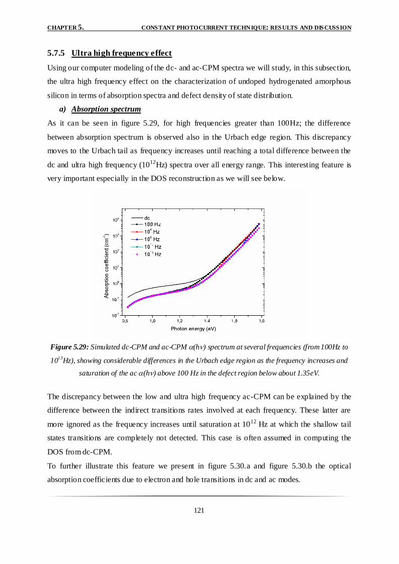
CHAPTER 5. CONSTANT PHOTOCURRENT TECHNIQUE: RESULTS AND DISCUSSION
121
5.7.5 Ultra high frequency effect
Using our computer modeling of the dc- and ac-CPM spectra we will study, in this subsection,
the ultra high frequency effect on the characterization of undoped hydrogenated amorphous
silicon in terms of absorption spectra and defect density of state distribution.
a) Absorption spectrum
As it can be seen in figure 5.29, for high frequencies greater than 100Hz; the difference
between absorption spectrum is observed also in the Urbach edge region. This discrepancy
moves to the Urbach tail as frequency increases until reaching a total difference between the
dc and ultra high frequency (1012Hz) spectra over all energy range. This interesting feature is
very important especially in the DOS reconstruction as we will see below.
Figure 5.29: Simulated dc-CPM and ac-CPM (h) spectrum at several frequencies (from 100Hz to
1013
Hz), showing considerable differences in the Urbach edge region as the frequency increases and
saturation of the ac (h) above 100 Hz in the defect region below about 1.35eV.
The discrepancy between the low and ultra high frequency ac-CPM can be explained by the
difference between the indirect transitions rates involved at each frequency. These latter are
more ignored as the frequency increases until saturation at 1012 Hz at which the shallow tail
states transitions are completely not detected. This case is often assumed in computing the
DOS from dc-CPM.
To further illustrate this feature we present in figure 5.30.a and figure 5.30.b the optical
absorption coefficients due to electron and hole transitions in dc and ac modes.
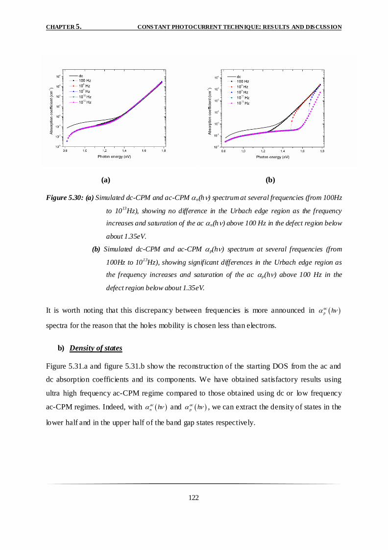
CHAPTER 5. CONSTANT PHOTOCURRENT TECHNIQUE: RESULTS AND DISCUSSION
122
(a) (b)
Figure 5.30: (a) Simulated dc-CPM and ac-CPM n(h) spectrum at several frequencies (from 100Hz
to 1013
Hz), showing no difference in the Urbach edge region as the frequency
increases and saturation of the ac n(h) above 100 Hz in the defect region below
about 1.35eV.
(b) Simulated dc-CPM and ac-CPM p(h) spectrum at several frequencies (from
100Hz to 1013
Hz), showing significant differences in the Urbach edge region as
the frequency increases and saturation of the ac p(h) above 100 Hz in the
defect region below about 1.35eV.
It is worth noting that this discrepancy between frequencies is more announced in ac
p h
spectra for the reason that the holes mobility is chosen less than electrons.
b) Density of states
Figure 5.31.a and figure 5.31.b show the reconstruction of the starting DOS from the ac and
dc absorption coefficients and its components. We have obtained satisfactory results using
ultra high frequency ac-CPM regime compared to those obtained using dc or low frequency
ac-CPM regimes. Indeed, with ac
n h and ac
p h , we can extract the density of states in the
lower half and in the upper half of the band gap states respectively.
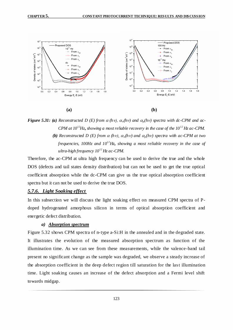
CHAPTER 5. CONSTANT PHOTOCURRENT TECHNIQUE: RESULTS AND DISCUSSION
123
(a) (b)
Figure 5.31: (a) Reconstructed D (E) from (h), n(h) and p(h) spectra with dc-CPM and ac-
CPM at 1012
Hz, showing a most reliable recovery in the case of the 1012
Hz ac-CPM.
(b) Reconstructed D (E) from (h), n(h) and p(h) spectra with ac-CPM at two
frequencies, 100Hz and 1012
Hz, showing a most reliable recovery in the case of
ultra-high frequency 1012
Hz ac-CPM.
Therefore, the ac-CPM at ultra high frequency can be used to derive the true and the whole
DOS (defects and tail states density distribution) but can not be used to get the true optical
coefficient absorption while the dc-CPM can give us the true optical absorption coefficient
spectra but it can not be used to derive the true DOS.
5.7.6. Light Soaking effect
In this subsection we will discuss the light soaking effect on measured CPM spectra of P-
doped hydrogenated amorphous silicon in terms of optical absorption coefficient and
energetic defect distribution.
a) Absorption spectrum
Figure 5.32 shows CPM spectra of n- type a-Si:H in the annealed and in the degraded state.
It illustrates the evolut ion of the measured absorption spectrum as function of the
illumination time. As we can see from these measurements, while the valence-band tail
present no significant change as the sample was degraded, we observe a steady increase of
the absorption coefficient in the deep defect region till saturation for the las t illumination
time. Light soaking causes an increase of the defect absorption and a Fermi level shift
towards midgap.
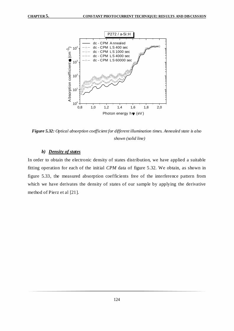
CHAPTER 5. CONSTANT PHOTOCURRENT TECHNIQUE: RESULTS AND DISCUSSION
124
0,8 1,0 1,2 1,4 1,6 1,8 2,010
0
101
102
103
104
P272 / a-Si :H
Ab
sorp
tio
n c
oeff
icie
nt
(cm
-1)
Photon energy h(eV )
dc - CPM A nnealed
dc - CPM L S 400 sec
dc - CPM L S 1000 sec
dc - CPM L S 4000 sec
dc - CPM L S 60000 sec
Figure 5.32: Optical absorption coefficient for different illumination times. Annealed state is also
shown (solid line)
b) Density of states
In order to obtain the electronic density of states distribution, we have applied a suitable
fitting operation for each of the init ial CPM data of figure 5.32. We obtain, as shown in
figure 5.33, the measured absorption coefficients free of the interference pattern from
which we have derivates the density of states of our sample by applying the derivative
method of Pierz et al [21].
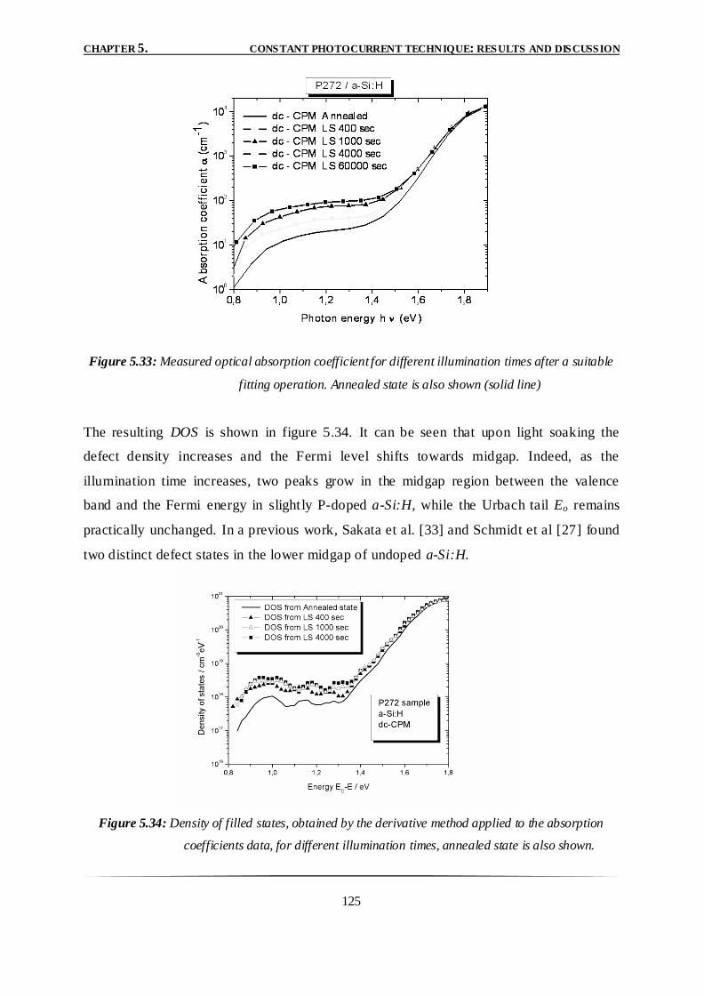
CHAPTER 5. CONSTANT PHOTOCURRENT TECHNIQUE: RESULTS AND DISCUSSION
125
Figure 5.33: Measured optical absorption coefficient for different illumination times after a suitable
fitting operation. Annealed state is also shown (solid line)
The resulting DOS is shown in figure 5.34. It can be seen that upon light soaking the
defect density increases and the Fermi level shifts towards midgap. Indeed, as the
illumination time increases, two peaks grow in the midgap region between the valence
band and the Fermi energy in slightly P-doped a-Si:H, while the Urbach tail Eo remains
practically unchanged. In a previous work, Sakata et al. [33] and Schmidt et al [27] found
two distinct defect states in the lower midgap of undoped a-Si:H.
Figure 5.34: Density of filled states, obtained by the derivative method applied to the absorption
coefficients data, for different illumination times, annealed state is also shown.
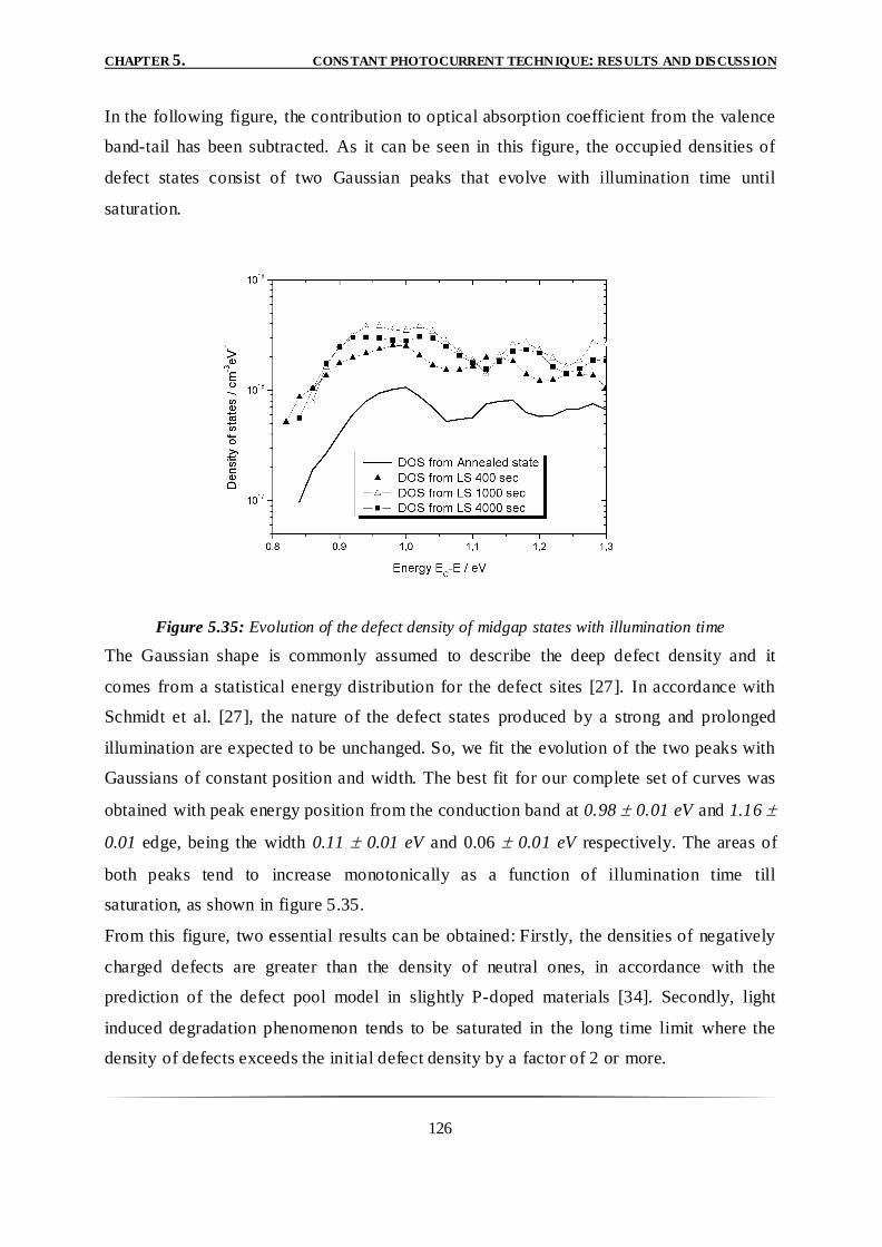
CHAPTER 5. CONSTANT PHOTOCURRENT TECHNIQUE: RESULTS AND DISCUSSION
126
In the following figure, the contribution to optical absorption coefficient from the valence
band-tail has been subtracted. As it can be seen in this figure, the occupied densities of
defect states consist of two Gaussian peaks that evolve with illumination time until
saturation.
Figure 5.35: Evolution of the defect density of midgap states with illumination time
The Gaussian shape is commonly assumed to describe the deep defect density and it
comes from a statistical energy distribution for the defect sites [27]. In accordance with
Schmidt et al. [27], the nature of the defect states produced by a strong and prolonged
illumination are expected to be unchanged. So, we fit the evolution of the two peaks with
Gaussians of constant position and width. The best fit for our complete set of curves was
obtained with peak energy position from the conduction band at 0.98 0.01 eV and 1.16
0.01 edge, being the width 0.11 0.01 eV and 0.06 0.01 eV respectively. The areas of
both peaks tend to increase monotonically as a function of illumination time till
saturation, as shown in figure 5.35.
From this figure, two essential results can be obtained: Firstly, the densities of negatively
charged defects are greater than the density of neutral ones, in accordance with the
prediction of the defect pool model in slightly P-doped materials [34]. Secondly, light
induced degradation phenomenon tends to be saturated in the long time limit where the
density of defects exceeds the init ial defect density by a factor of 2 or more.
CHAPTER 5. CONSTANT PHOTOCURRENT TECHNIQUE: RESULTS AND DISCUSSION
127
References
[1] Jackson W B, Amer N M, Boccara A C and Fournier D 1981 Applied Optics 20 (8) 1333-
44.
[2] Vanecek M, Kocka J, Poruba A and Fejfar A 1995 J. Appl. Phys. 78 (10) 6203-10.
[3] Fejfar A, Poruba A, Vanecek M and Kocka J 1996 Journal of Non-Crystalline Solids 198-
200 304-308.
[4] Hattori K, Adachi Y, Anzai M, Okamoto H and Hamakawa Y 1994 J. Appl. Phys. 76 (5)
2841-50.
[5] Schauer F, Eliat A, Nesladek M and Adriaenssens G J 1994 Appl. Phys. Lett. 64 (22)
3009-11.
[6] Pickin W, Alonzo J C and Mendoza D 1987 J. Phys. C: Solid State Phys. 20 341-345.
[7] Sladek P, Stahel P and Theye M L 1995 Philosophical Magazine B 71 (5) 871-880.
[8] K. Hattori, S. Fukuda, K. Nishimura, H. Okamoto, and Y. Hamakawa, Journal of Non-
Crystalline Solids 164-166 (1993) 351-354.
[9] Sauvain E, Mettler A, Wyrsch N and Shah A 1993 Solid State Communications 85 (3)
219-222.
[10] Shimizu T, Sugiyama H and Kumeda M 2001 Solar Energy Materials and Solar Cells 66
203-207.
[11] Bube R H, Benatar L E, Grimbergen M N and Redfield D 1992 J. Appl. Phys. 72(12)
5766-77.
[12] Mettler A, Wyrsch N, Goetz M and Shah A 1994 Solar Energy Materials and Solar Cells
34 533-539.
[13] Zhang Q and Adriaenssens G J 1997 J. Appl. Phys. 81(10) 6795-99.
[14] Schmidt J A, Koropecki R R, Arce R D, Rubinelli F A and Buitrago R H 2000 Thin Solid
Films 376 267-274.
[15] Conte G, Irrena F, Nobile G and Palma F 1993 Journal of Non-Crystalline Solids 164-
166 419-22.
[16] Sladek P and Theye M L 1994 Solid State Communications 89 (3) 199-203.
[17] Hasegawa S, Nitta S and Nonomura S 1996 Journal of Non Crystalline Solids 198-200
544-547.
[18] C. Main, S. Reynolds, I. Zrinscak and A. Merazga Journal of Non Crystalline Solids
338-340 (2004), 228-231.
CHAPTER 5. CONSTANT PHOTOCURRENT TECHNIQUE: RESULTS AND DISCUSSION
128
[19] A. Merazga, “Steady state and transient photoconductivity in n-type a-Si”, PhD. thesis,
Dundee Institute of Technology, Dundee, UK, 1990.
[20] D. Ritter and K. Weiser, Optics Communications Vol.57, No. 5, pp.336-338, 1986.
[21] K. Pierz , B. Hilgenberg, H. Mell and G. Weiser, Journal of Non-Crystalline Solids 97-
98, 1987, pp. 63-66.
[22] S. Heck, “Investigation of light- induced defects in hydrogenated amorphous silicon by
low temperature annealing and pulsed degradation”, PhD Thesis, der Philipps-Universitat
Marburg, Marburg/Lahn 2002.
[23] J. Tauc, R. Grigorovici and A. Vancu, Phys. Stat. Sol. 15 (1966), 627
[24] R. H. Klazes, M. H. L. M. van der Broek, J. Bezemer and S. Radelaar, Philos. Mag. 45
(1983) 377.
[25] S. Nitta, S. Itoh, M. Tanaka, T. Endo and A. Hatano, Sol. Energy Mater. 8 (1982) 249.
[26] T. Searle, “Properties of Amorphous Silicon and its Alloys”, Edited by University of
Sheffield, UK, 1998.
[27] J. A. Schmidt, R. Arce, R.H. Buitrago, and R. R. Koropecki , Physical Review B, Vol.
55, No.15, pp. 9621-9627, April 1997-1.
[28] C. Main, S. Reynolds, I. Zrinscak and A. Merazga, Journal of Materials Science-
Materials in Electronics, 14 681-684, 2003.
[29] S. Reynolds, V. Smirnov, C. Main, R. Carius and F. Finger, Mat. Res. Soc. Symp. Proc.
Vol. 715 © Materials Research Society, 2002.
[30] Von Thorsten Dylla, “Electron Spin Resonance and Transient Photocurrent
Measurements on Microcrystalline Silicon”, PhD. thesis, Fachbereich Physik, Freie
Universität Berlin, Germany, 2004.
[31] H. Belgacem, A. Merazga and C. Longeaud, Semiconductor Science and Technology 20
(2005) 56-61.
[32] C. Longeaud, J. P. Kleider, P. Kaminski, R. Kozlowski, M. Pawlowski, and J. Cwirko,
Semiconductor Science and Technology 14 (1999) 747-756.
[33] I. Sakata, M. Yamanaka, S. Numase, and Y. Hayashi, J. Appl. Phys. , 71 (9), 4344-4353,
1992.
[34] J. Schmal, Journal of Non-Crystalline Solids, 198-200, 387-390, 1996.
CHAPTER 6. GENERAL CONCLUSIONS
129
CHAPTER 6
GENERAL CONCLUSIONS
6.1. Conclusions
Constant Photocurrent Method (CPM) has been used extensively as a means of characterising
thin film semiconductors. CPM measurements using steady (dc) or modulated (ac) sub-gap
excitation permit the determination of the optical absorption associated with the density of
defect states (DOS). However, slow photoresponse times in materials like a-Si:H often
influence the ac measurement, and hence optical absorption spectra obtained by ac and dc-
CPM can be very different.
In the present work, both measurements and numerical simulation of CPM absorption
spectrum for dc and ac optical excitation conditions have been carried out to determine the
density of gap-states distribution in amorphous and crystalline semiconductors such as a-
Si:H/c-Si:H , as typical of amorphous semiconductors and GaAs as typical of crystalline
semiconductors.
For this reason, a general numerical simulation program of dc and ac constant photocurrent
method (dc-CPM and ac-CPM) has been developed. This code program is based on several
density of states models typical for hydrogenated amorphous silicon (a-Si:H), hydrogenated
microcrystalline silicon (c-Si:H) and gallium arsenide (GaAs) materials and take into
account all possible thermal and optical transitions between localised states and extended
states.
For the case of hydrogenated amorphous silicon both intrinsic and n-type, a density of states
(DOS) model has been chosen according to the improved defect pool model (DPM) of Powell
CHAPTER 6. GENERAL CONCLUSIONS
130
and Dean. The density of states models for microcrystalline silicon and gallium arsenide have
been taken from literature with appropriate parameters.
In addition, we have performed experimental measurement of CPM on semiconductor
materials with applications in solar energy. In order to validate the simulation results,
measurements of dc and ac-CPM have been performed particularly on the following samples:
intrinsic and doped a-Si:H (Intersolar ISB4, P272) and c-Si:H (00c354) and also semi-
insulating Cr- doped GaAs (SI GaAs:Cr #1713)..
We have presented in this thesis the difference observed for the optical absorption coefficients
and the density of deep defect states between the ac and the dc modes.
The difference in ac and dc absorption spectra arises from the frequency dependence of the
different excitation pathways by which free electrons and free holes can be produced by sub-
gap excitation. ac modulated excitation will reveal absorption associated with transitions from
occupied states below Fermi level EF, into the conduction band, while dc excitation will
include transitions from the valence band into unoccupied defect states above EF, followed by
slow thermal emission to the conduction band. In the other hand, analysis of the n (h) and
p (h) absorption spectrum components corresponding to optical transitions associated with
free electrons and free holes creation, respectively, allows the two regions of the DOS, above
and below the Fermi level, to be determined. So, we have been able to obtain the density of
states distribution within the gap of such semiconductors materials by applying the derivative
method of Pierz et al to the both dc- (h) and ac- (h) data and also to the experimentally
inaccessible components n (h) and p (h).
We report on the use of this method in studying the effects of high frequency on different
regions of the DOS in a-Si:H (especially ultra high frequency).
Comparative analysis of DOS distributions, determined from the dc and ac-CPM at
frequencies in the range 1-102Hz, results in the conclusion that, the indirect transitions
involving subsequent slow thermal emissions are responsible of the difference between
different frequency-ac-CPM-determined DOS. Consequently, at sufficiently high frequency,
compared to thermal emission rates, the occupied states below the quasi-Fermi level are
revealed from the n (h) spectra, while the empty states are revealed from the p (h)
spectra. High frequency ac-CPM is, therefore, most reliable as a spectroscopy method for the
DOS distribution.
CHAPTER 6. GENERAL CONCLUSIONS
131
Furthermore, at ultra-high frequency in the range 102-1013Hz, the entire ac-CPM-determined
DOS distribution could be reliably determined by deconvolution of both absorption
coefficient spectra ac
n h and ac
p h . Our simulations reveal that the dc-CPM and the ac-
CPM at ultra-high frequency yield optical absorption spectra with significant differences, not
only below the Urbach edge, as for low frequency ac-CPM, but also in the Urbach edge. The
reliability to infer the DOS distribution by deconvolution of both ac
n h and ac
p h
spectra at ultra-high frequency is demonstrated.
In this thesis, by using the constant photocurrent measurement in dc-mode, we have
investigated the effect of the light soaking (LS) on the deep defect density (Nd) and the
slope of the Urbach tail (Eo) of the slightly P-doped a-Si:H film prepared by PECVD in
term of evolution of the measured sub-gap absorption coefficient and density of states
distribution as function of illumination time. The derivative method applied to the dc-
(h) data allowed us to obtain the occupied density of states. The measurement results
in terms of absorption spectrum and deep defect density shows an increase of both with
illumination time untill saturation. The dominant metastable defects are the dangling
bonds. In fact, their densities pass from 5x1017cm-3 eV-1 in an init ial state to 5x1018cm-3
eV-1 in a degraded state while the tail states remains basically constant. The DOS showed
the presence of two Gaussian distribution between the valence band and the Fe rmi energy
with two peaks. These two peaks have constant positions and widths which do not
changed considerably with illumination. We have assigned the peak closer to the valence
band to the negatively charged defects D- and the other peak (midgap peak) to the neutral
dangling bonds Do. We have also found that the densit ies of both defects grow as 1/ 3illt .
This is in agreement with ESR measurements, which show a spin density growing with
the same time dependence.
The electronic properties of microcrystalline silicon films have been studied in the present
thesis, by using constant photocurrent technique in ac regime. We have employed the
numerical computer program of ac-CPM to elucidate the experimental results. Analyzing the
measured and simulated absorption coefficients, it was found that the density of valence band-
tail states falls exponentially towards the gap with a typical band-tail width of 63 meV and a
conduction band tail slope of some 30 meV. Combining the information derived in this work
CHAPTER 6. GENERAL CONCLUSIONS
132
a schematic picture of the density of states in energetic sense has been obtained. Our study
indicates then that the constant photocurrent method is able to extract the whole density of
localized states in highly-crystalline c-Si:H films.
Finally, constant photocurrent method (CPM) is used to investigate the defect levels from the
optical absorption spectra of semi- insulating Cr-doped GaAs. By deconvolution of the optical
absorption spectrum, we have extracted the distribution of the density of states within the gap.
We have developed a computer code program which has been used to reconstruct the
measured dc and ac- CPM optical absorption spectrum by using the extracted density of states
as a model of state distribution. It is also found that with the application of the two
complementary techniques: constant photocurrent method (CPM) and modulated photocurrent
(MPC), we are able to have a full reconstruction of the density of states distribution for such
materials.
As a conclusion, the dc method have usually been favored in measurement of optical
absorption whereas the ac measurements using high chopping frequency is to be preferred to
yield to the true density of states distribution. Hence dc- and ac-CPM should be used both as a
useful spectroscopy methods for materials characterisation.
6.2. Suggestions for further work
However, we believe that there is still much to do. For example, in recently paper Main et al.
reported that the detail knowledge of the differences in ac- and dc- derived absorption spectra
give us the possibility to use both ac and dc CPM, not only to obtain information on the DOS
below the Fermi level EF - i.e. occupied states, but also on the density of unoccupied states
above EF .
So, we suggest, in one side, to exploring the differences and similarities between dc and ac-
CPM which can be helpful to characterise various materials (nano-, micro-, poly crystalline,
polymorphous silicon,…etc) with both configuration coplanar (films) and sandwich (solar
cells and photoconductors). On the other side, the combination of several similar techniques
(CPM, PDS and MPC even TPC and SCLC TOF) can lead to a successful characterisation of
such variety and new materials with applications in solar cells and photodetectors.

AAPPPPEENNDDIICCEESS
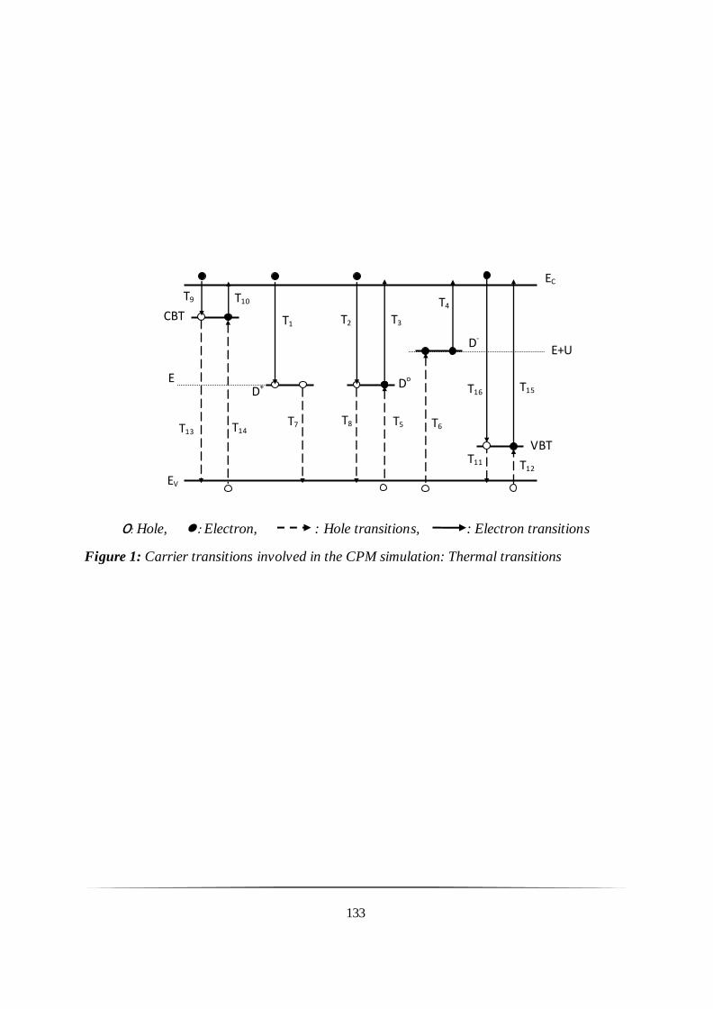
133
o: Hole, ●: Electron, : Hole transitions, : Electron transitions
Figure 1: Carrier transitions involved in the CPM simulation: Thermal transitions
EC
EV
E
E+U
CBT
VBT
Do
D-
D+
T1 T2 T3
T4
T5 T6 T8 T7
T9 T10
T11 T12
T13
T15
T14
T16
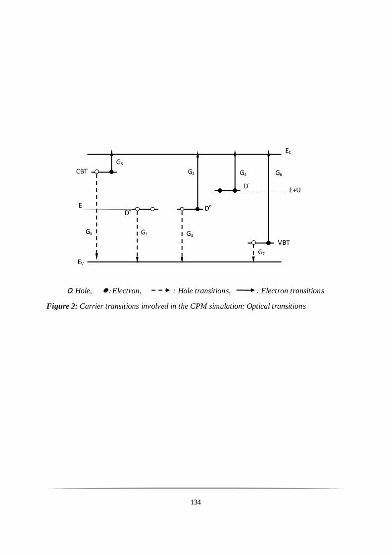
134
o: Hole, ●: Electron, : Hole transitions, : Electron transitions
Figure 2: Carrier transitions involved in the CPM simulation: Optical transitions
EC
EV
E
E+U
CBT
VBT
Do
D-
D+
G1
G2
G3
G4
G5
G6
G7
G8
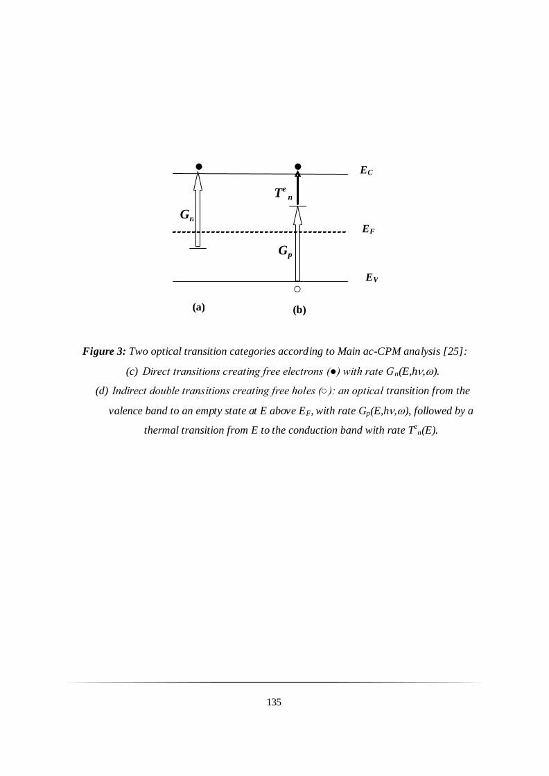
135
Figure 3: Two optical transition categories according to Main ac-CPM analysis [25]:
(c) Direct transitions creating free electrons (●) with rate Gn(E,h).
(d) Indirect double transitions creating free holes (○): an optical transition from the
valence band to an empty state at E above EF, with rate Gp(E,h), followed by a
thermal transition from E to the conduction band with rate Ten(E).
EC
EV
(b)
(a)
EF
●
●
○
G p
G n
T e n
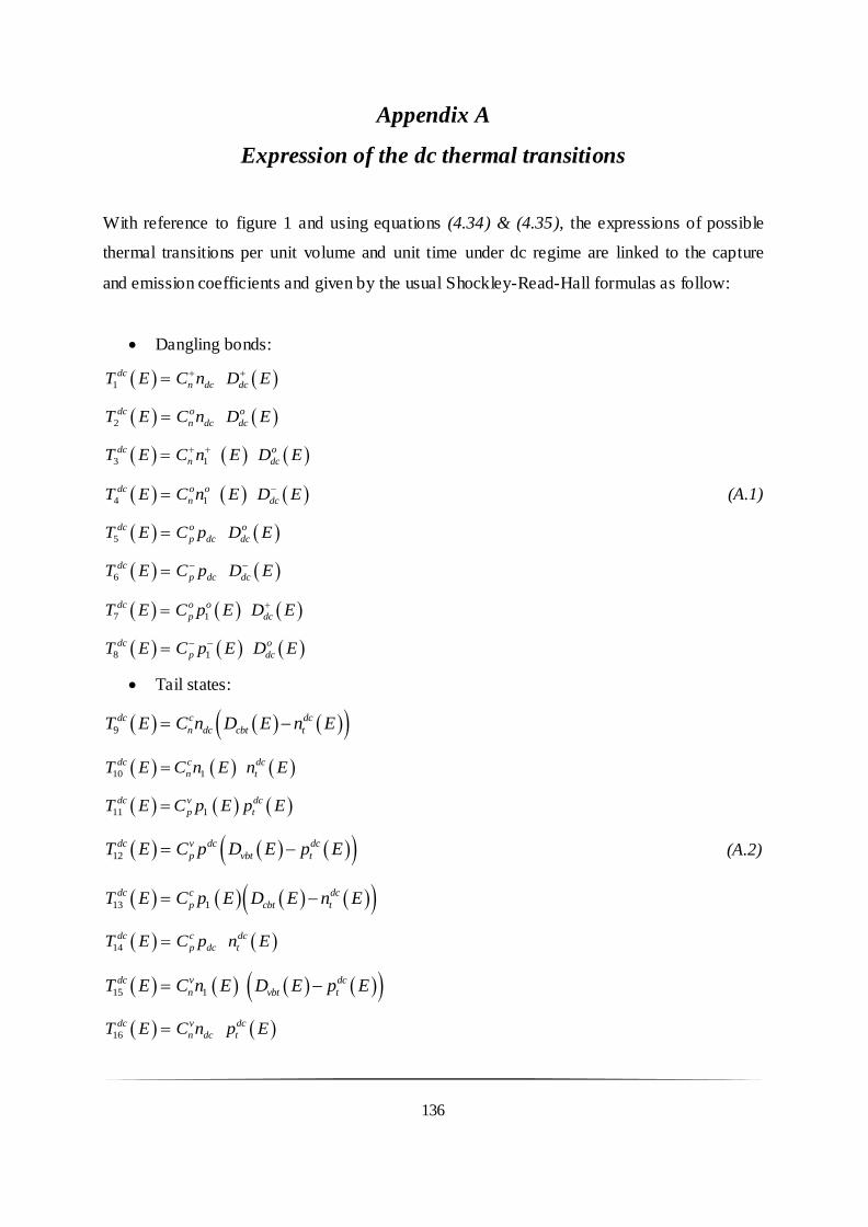
136
Appendix A
Expression of the dc thermal transitions
With reference to figure 1 and using equations (4.34) & (4.35), the expressions of possible
thermal transitions per unit volume and unit time under dc regime are linked to the capture
and emission coefficients and given by the usual Shockley-Read-Hall formulas as follow:
Dangling bonds:
1
dc
n dc dcT E C n D E
2
dc o o
n dc dcT E C n D E
3 1
dc o
n dcT E C n E D E
4 1
dc o o
n dcT E C n E D E (A.1)
5
dc o o
p dc dcT E C p D E
6
dc
p dc dcT E C p D E
7 1
dc o o
p dcT E C p E D E
8 1
dc o
p dcT E C p E D E
Tail states:
9
dc c dc
n dc cbt tT E C n D E n E
10 1
dc c dc
n tT E C n E n E
11 1
dc v dc
p tT E C p E p E
12
dc v dc dc
p vbt tT E C p D E p E (A.2)
13 1
dc c dc
p cbt tT E C p E D E n E
14
dc c dc
p dc tT E C p n E
15 1
dc v dc
n vbt tT E C n E D E p E
16
dc v dc
n dc tT E C n p E
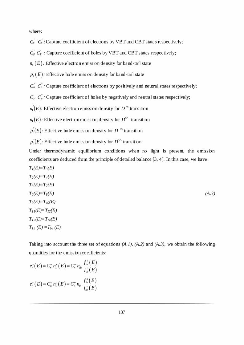
137
where:
v
nC c
nC : Capture coefficient of electrons by VBT and CBT states respectively;
v
pCc
pC : Capture coefficient of holes by VBT and CBT states respectively;
1n E : Effective electron emission density for band-tail state
1p E : Effective hole emission density for band-tail state
nC0
nC : Capture coefficient of electrons by positively and neutral states respectively;
pC0
pC : Capture coefficient of holes by negatively and neutral states respectively;
En0
1 : Effective electron emission density for D-/o transition
En
1 : Effective electron emission density for Do/+ transition
Ep0
1 : Effective hole emission density for D+/o transition
Ep
1 : Effective hole emission density for Do/- transition
Under thermodynamic equilibrium conditions when no light is present, the emission
coefficients are deduced from the principle of detailed balance [3, 4]. In this case, we have:
T1(E)=T3(E)
T2(E)=T4(E)
T5(E)=T7(E)
T6(E)=T8(E) (A.3)
T9(E)=T10(E)
T11(E)=T12(E)
T13(E)=T14(E)
T15 (E) =T16 (E)
Taking into account the three set of equations (A.1), (A.2) and (A.3), we obtain the following
quantities for the emission coefficients:
1
tho
n n n th o
th
f Ee E C n E C n
f E
1
o
tho o o
n n n th
th
f Ee E C n E C n
f E
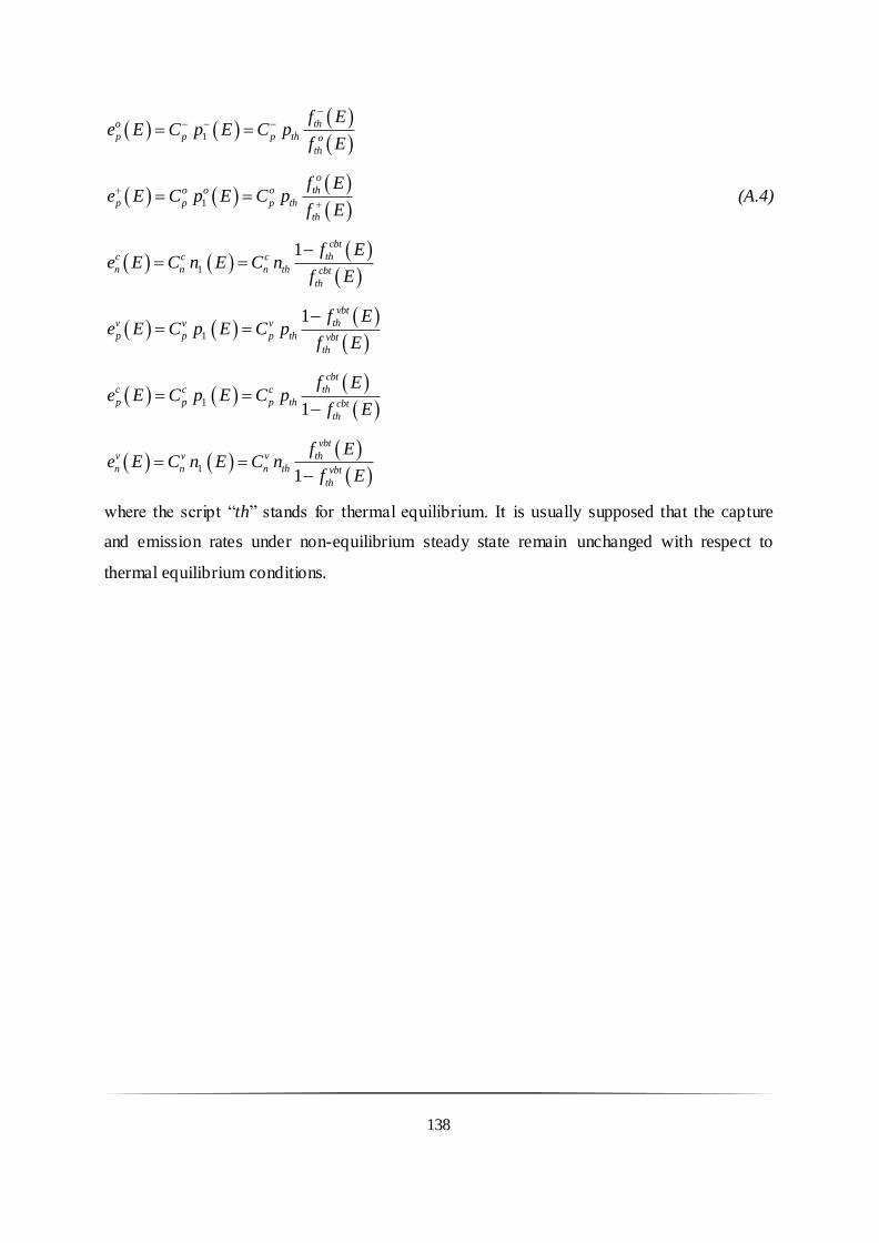
138
1
tho
p p p th o
th
f Ee E C p E C p
f E
1
o
tho o o
p p p th
th
f Ee E C p E C p
f E
(A.4)
1
1 cbt
thc c c
n n n th cbt
th
f Ee E C n E C n
f E
1
1 vbt
thv v v
p p p th vbt
th
f Ee E C p E C p
f E
1
1
cbt
thc c c
p p p th cbt
th
f Ee E C p E C p
f E
1
1
vbt
thv v v
n n n th vbt
th
f Ee E C n E C n
f E
where the script “th” stands for thermal equilibrium. It is usually supposed that the capture
and emission rates under non-equilibrium steady state remain unchanged with respect to
thermal equilibrium conditions.
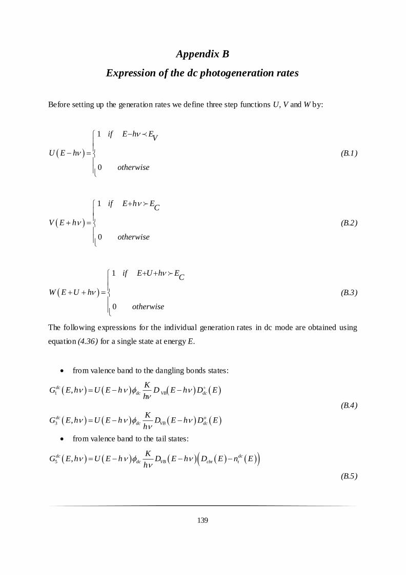
139
Appendix B
Expression of the dc photogeneration rates
Before setting up the generation rates we define three step functions U, V and W by:
1
0
if E h EV
U E h
otherwise
(B.1)
1
0
if E h EC
V E h
otherwise
(B.2)
1
0
if E U h EC
W E U h
otherwise
(B.3)
The following expressions for the individual generation rates in dc mode are obtained using
equation (4.36) for a single state at energy E.
from valence band to the dangling bonds states:
1 ,dc
dc VB dc
KG E h U E h D E h D E
h
(B.4)
3 ,dc o
dc VB dc
KG E h U E h D E h D E
h
from valence band to the tail states:
5 ,dc dc
dc VB cbt t
KG E h U E h D E h D E n E
h
(B.5)
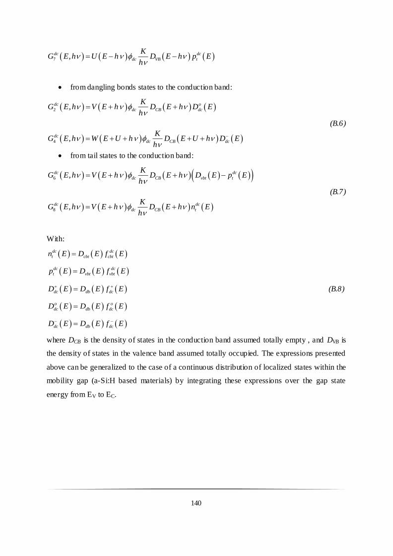
140
7 ,dc dc
dc VB t
KG E h U E h D E h p E
h
from dangling bonds states to the conduction band:
2 ,dc o
dc CB dc
KG E h V E h D E h D E
h
(B.6)
4 ,dc
dc CB dc
KG E h W E U h D E U h D E
h
from tail states to the conduction band:
6 ,dc dc
dc CB vbt t
KG E h V E h D E h D E p E
h
(B.7)
8 ,dc dc
dc CB t
KG E h V E h D E h n E
h
With:
dc dc
t cbt cbtn E D E f E
dc dc
t vbt vbtp E D E f E
dc db dcD E D E f E
(B.8)
o o
dc db dcD E D E f E
dc db dcD E D E f E
where DCB is the density of states in the conduction band assumed totally empty , and DVB is
the density of states in the valence band assumed totally occupied. The expressions presented
above can be generalized to the case of a continuous distribution of localized states within the
mobility gap (a-Si:H based materials) by integrating these expressions over the gap state
energy from EV to EC.
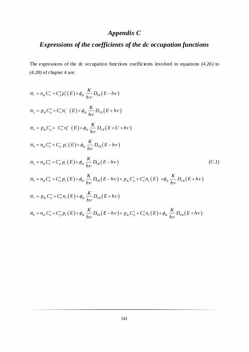
141
Appendix C
Expressions of the coefficients of the dc occupation functions
The expressions of the dc occupation functions coefficients involved in equations (4.26) to
(4.28) of chapter 4 are:
1 1
o o
dc n p dc VB
Ktt n C C p E D E h
h
2 1
o
dc p n dc CB
Ktt p C C n E D E h
h
3 1
o o
dc p n dc CB
Ktt p C C n E D E U h
h
4 1
o
dc n p dc VB
Ktt n C C p E D E h
h
5 1
c c
dc n p dc VB
Ktt n C C p E D E h
h
(C.1)
6 1 1
c c c c
dc n p dc VB dc p n dc CB
K Ktt n C C p E D E h p C C n E D E h
h h
7 1
v v
dc p n dc CB
Ktt p C C n E D E h
h
8 1 1
v v v v
dc n p dc VB dc p n dc CB
K Ktt n C C p E D E h p C C n E D E h
h h
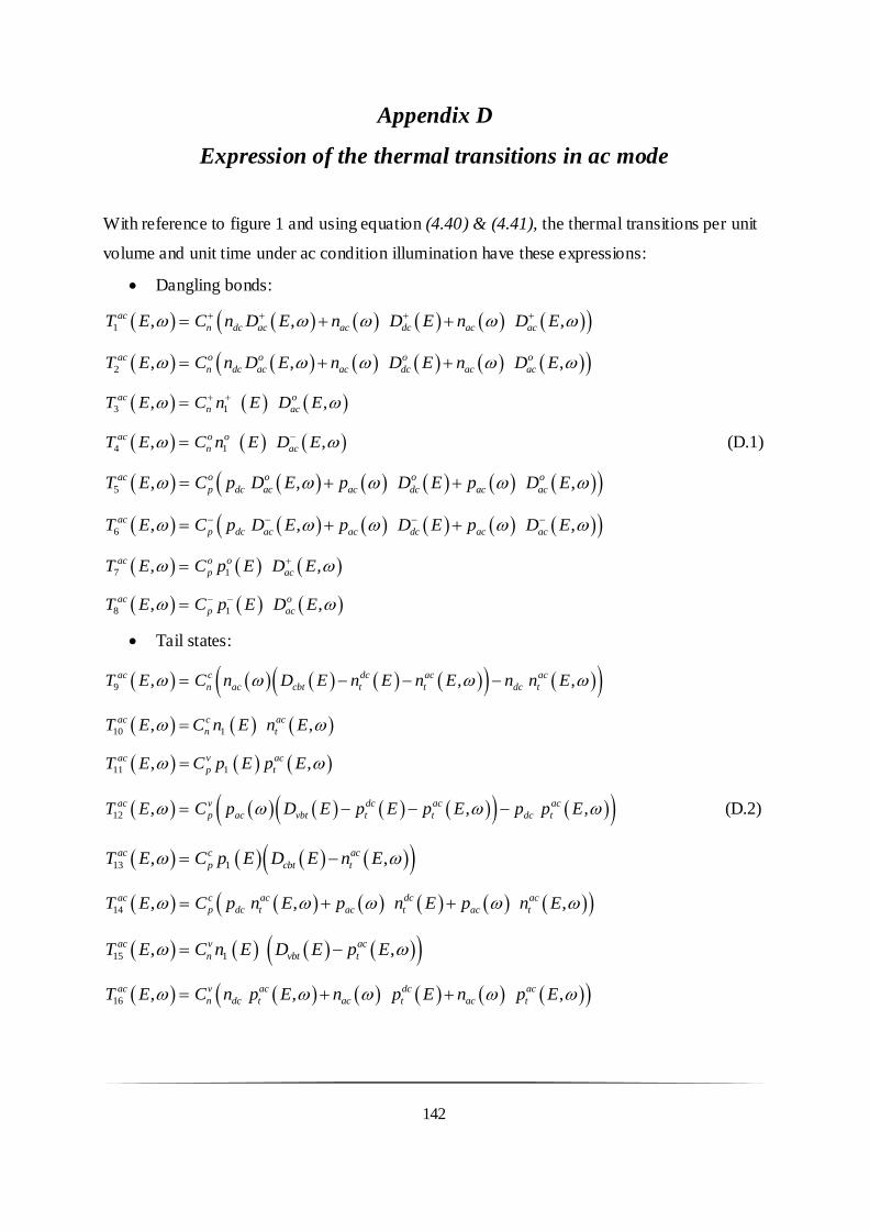
142
Appendix D
Expression of the thermal transitions in ac mode
With reference to figure 1 and using equation (4.40) & (4.41), the thermal transitions per unit
volume and unit time under ac condition illumination have these expressions:
Dangling bonds:
1 , , ,ac
n dc ac ac dc ac acT E C n D E n D E n D E
2 , , ,ac o o o o
n dc ac ac dc ac acT E C n D E n D E n D E
3 1, ,ac o
n acT E C n E D E
4 1, ,ac o o
n acT E C n E D E (D.1)
5 , , ,ac o o o o
p dc ac ac dc ac acT E C p D E p D E p D E
6 , , ,ac
p dc ac ac dc ac acT E C p D E p D E p D E
7 1, ,ac o o
p acT E C p E D E
8 1, ,ac o
p acT E C p E D E
Tail states:
9 , , ,ac c dc ac ac
n ac cbt t t dc tT E C n D E n E n E n n E
10 1, ,ac c ac
n tT E C n E n E
11 1, ,ac v ac
p tT E C p E p E
12 , , ,ac v dc ac ac
p ac vbt t t dc tT E C p D E p E p E p p E (D.2)
13 1, ,ac c ac
p cbt tT E C p E D E n E
14 , , ,ac c ac dc ac
p dc t ac t ac tT E C p n E p n E p n E
15 1, ,ac v ac
n vbt tT E C n E D E p E
16 , , ,ac v ac dc ac
n dc t ac t ac tT E C n p E n p E n p E
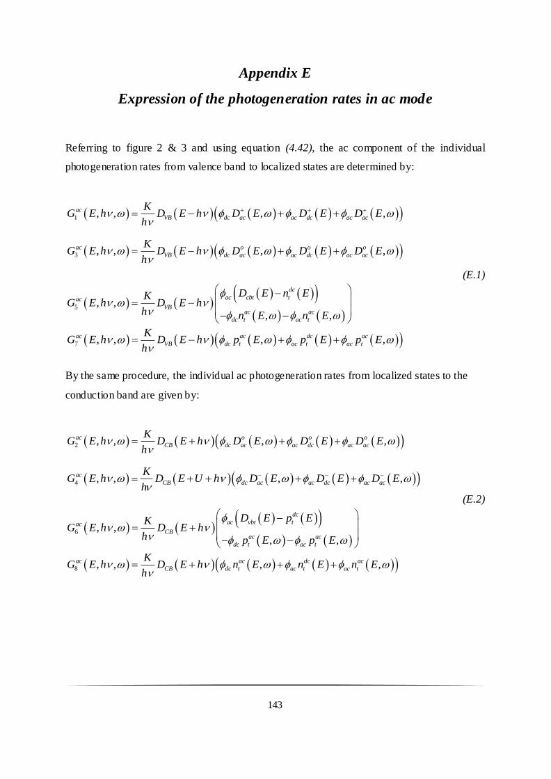
143
Appendix E
Expression of the photogeneration rates in ac mode
Referring to figure 2 & 3 and using equation (4.42), the ac component of the individual
photogeneration rates from valence band to localized states are determined by:
1 , , , ,ac
VB dc ac ac dc ac ac
KG E h D E h D E D E D E
h
3 , , , ,ac o o o
VB dc ac ac dc ac ac
KG E h D E h D E D E D E
h
(E.1)
5 , ,
, ,
dc
ac cbt tac
VBac ac
dc t ac t
D E n EKG E h D E h
h n E n E
7 , , , ,ac ac dc ac
VB dc t ac t ac t
KG E h D E h p E p E p E
h
By the same procedure, the individual ac photogeneration rates from localized states to the
conduction band are given by:
2 , , , ,ac o o o
CB dc ac ac dc ac ac
KG E h D E h D E D E D E
h
4 , , , ,ac
CB dc ac ac dc ac ac
KG E h D E U h D E D E D E
h
(E.2)
6 , ,
, ,
dc
ac vbt tac
CBac ac
dc t ac t
D E p EKG E h D E h
h p E p E
8 , , , ,ac ac dc ac
CB dc t ac t ac t
KG E h D E h n E n E n E
h
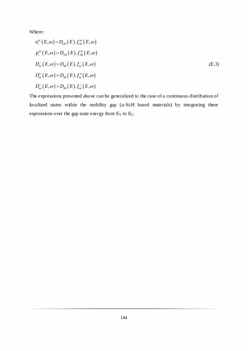
144
Where:
, . ,ac ac
t cbt cbtn E D E f E
, . ,ac ac
t vbt vbtp E D E f E
, . ,ac db acD E D E f E (E.3)
, . ,o o
ac db acD E D E f E
, . ,ac db acD E D E f E
The expressions presented above can be generalized to the case of a continuous distribution of
localized states within the mobility gap (a-Si:H based materials) by integrating these
expressions over the gap state energy from EV to EC.
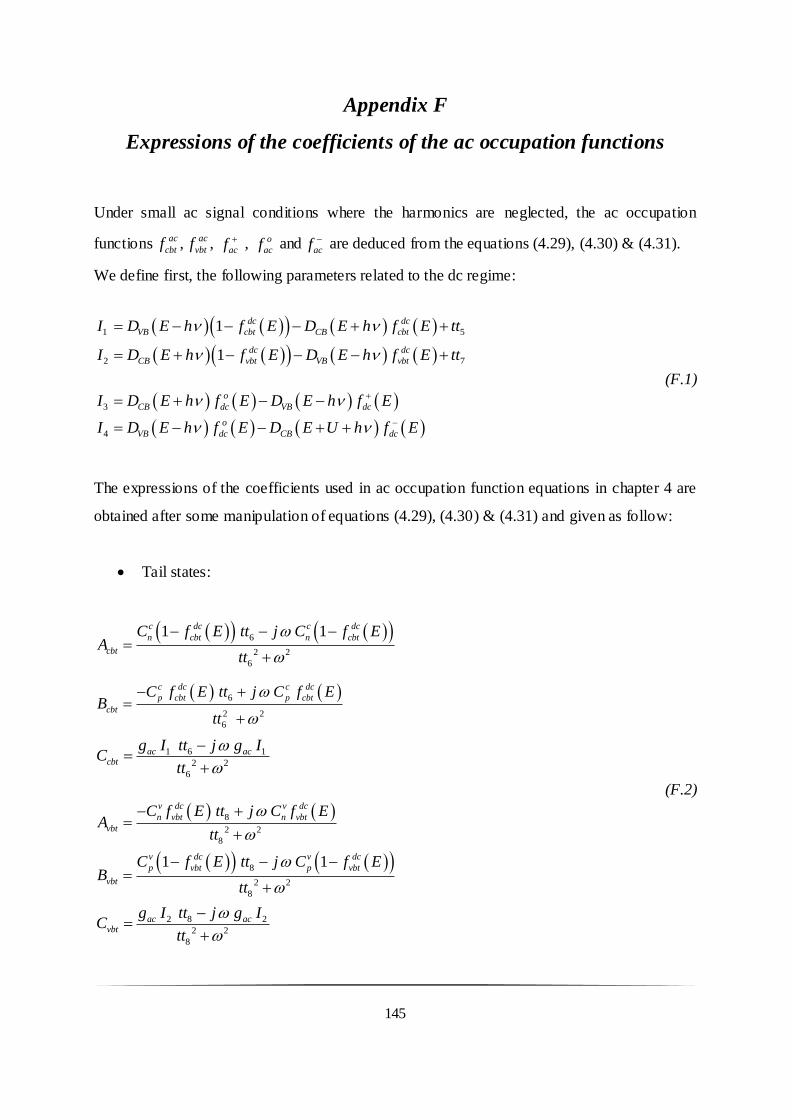
145
Appendix F
Expressions of the coefficients of the ac occupation functions
Under small ac signal conditions where the harmonics are neglected, the ac occupation
functions ac
cbtf , ac
vbtf , acf , o
acf andacf are deduced from the equations (4.29), (4.30) & (4.31).
We define first, the following parameters related to the dc regime:
1 51 dc dc
VB cbt CB cbtI D E h f E D E h f E tt
2 71 dc dc
CB vbt VB vbtI D E h f E D E h f E tt
(F.1)
3
o
CB dc VB dcI D E h f E D E h f E
4
o
VB dc CB dcI D E h f E D E U h f E
The expressions of the coefficients used in ac occupation function equations in chapter 4 are
obtained after some manipulation of equations (4.29), (4.30) & (4.31) and given as follow:
Tail states:
6
2 2
6
1 1c dc c dc
n cbt n cbt
cbt
C f E tt j C f EA
tt
6
2 2
6
c dc c dc
p cbt p cbt
cbt
C f E tt j C f EB
tt
1 6 1
2 2
6
ac accbt
g I tt j g IC
tt
(F.2)
8
2 2
8
v dc v dc
n vbt n vbt
vbt
C f E tt j C f EA
tt
8
2 2
8
1 1v dc v dc
p vbt p vbt
vbt
C f E tt j C f EB
tt
2 8 2
2 2
8
ac acvbt
g I tt j g IC
tt
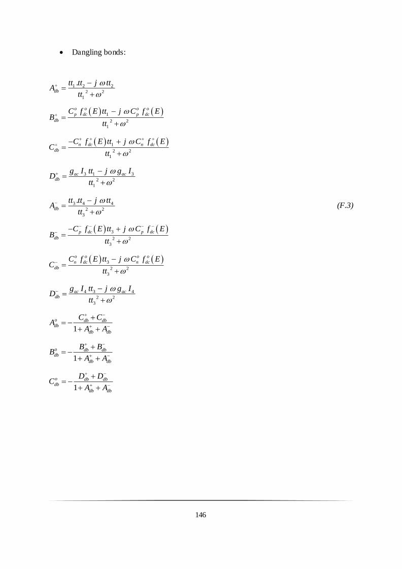
146
Dangling bonds:
1 2 2
2 2
1
.db
tt tt j ttA
tt
1
2 2
1
o o o o
p dc p dc
db
C f E tt j C f EB
tt
1
2 2
1
n dc n dc
db
C f E tt j C f EC
tt
3 1 3
2 2
1
ac acdb
g I tt j g ID
tt
3 4 4
2 2
3
.db
tt tt j ttA
tt
(F.3)
3
2 2
3
p dc p dc
db
C f E tt j C f EB
tt
3
2 2
3
o o o o
n dc n dc
db
C f E tt j C f EC
tt
4 3 4
2 2
3
ac acdb
g I tt j g ID
tt
1
o db dbdb
db db
C CA
A A
1
o db dbdb
db db
B BB
A A
1
o db dbdb
db db
D DC
A A