OBSERVER : ONDES ET MATIERE (1ère partie). Chapitre 1 : Ondes à travers l'espace, ondes sur Terre.
UNIVERSITÉ DE MONTRÉAL
MÉCANISMES PHYSIQUES ET FONDEMENTS THÉORIQUES DE LA RÉCUPÉRATION
D’ÉNERGIE MICRO-ONDES AMBIANTE POUR LES DISPOSITIFS SANS FIL À FAIBLE
CONSOMMATION
CARLOS HENRIQUE PETZL LORENZ
DÉPARTEMENT DE GÉNIE ÉLECTRIQUE
ÉCOLE POLYTECHNIQUE DE MONTRÉAL
MÉMOIRE PRÉSENTÉ EN VUE DE L’OBTENTION
DU DIPLÔME DE MAÎTRISE ÈS SCIENCES APPLIQUÉES
(GÉNIE ÉLECTRIQUE)
DÉCEMBRE 2015
© Carlos Henrique Petzl Lorenz, 2015.

UNIVERSITÉ DE MONTRÉAL
ÉCOLE POLYTECHNIQUE DE MONTRÉAL
Ce mémoire intitulé :
MÉCANISMES PHYSIQUES ET FONDEMENTS THÉORIQUES DE LA RÉCUPÉRATION
D’ÉNERGIE MICRO-ONDES AMBIANTE POUR LES DISPOSITIFS SANS FIL À FAIBLE
CONSOMMATION
présenté par : PETZL LORENZ Carlos Henrique
en vue de l’obtention du diplôme de : Maîtrise ès Sciences Appliquées
a été dûment accepté par le jury d’examen constitué de :
M. LAURIN Jean-Jacques, Ph. D., président
M. WU Ke, Ph. D., membre et directeur de recherche
M. CONSTANTIN Nicolas, Ph. D., membre

iii
DÉDICACE
À mon épouse Antonia Yume Eiri Trebien Lorenz, qui m’a appuyé inconditionnellement pendant
la maîtrise,
à mes parents Curt et Cristina Lorenz, qui m’ont enseigné l’importance de persévérer et de me
dévouer au travail, mais aussi de garder du temps pour la famille et les amis,
à Simon Hemour pour m’avoir guidé pendant ce travail de recherche et pour toujours avoir été
présent pour discuter de nouvelles idées.

iv
REMERCIEMENTS
Je tiens à remercier en premier lieu à Dieu pour toutes ses bénédictions qu’il m’a offertes.
Je tiens aussi à exprimer mes remerciements sincères à mon directeur de recherche,
professeur Ke Wu, par son soutien et ses conseils donnés au cours de mes travaux de recherches;
aussi comme par son soutien lors de mes moments de doute.
Un gros merci à Simon Hemour, qui était toujours présent pour discuter de nouvelles idées
et méthodes pour résoudre les problèmes auxquelles j’ai fait face. Je suis certain que sans ton aide
ce travail ne serait pas arrivé si loin.
Je voulais aussi remercier à tous les membres de l’équipe technique de Poly GRAMES,
par leur soutien dans les fabrication et caractérisation des prototypes, aussi bien que par leur support
informatique, à savoir Jules Gauthier, Traian Antonescu, Maxime Thibault, Steve Dubé et Jean-
Sébastien Décarie. Je tiens aussi à remercier à Nathalie Levesque de l'École Polytechnique qui m’a
toujours aidé lorsque des problèmes administratifs apparaissaient.
Je veux également remercier les membres du jury pour le temps qu'ils ont passé à la révision
de ce mémoire. Et aux collègues de Poly GRAMES qui ont contribué directement ou indirectement
au bon déroulement de ma maîtrise.
Je tiens finalement à exprimer ma plus profonde gratitude à mon épouse Antonia Yume Eiri
Trebien Lorenz pour son soutien inconditionnel tout au long de ces années de maîtrise, et aussi à
mes parents Curt et Cristina Lorenz qui ont mis plusieurs de leurs années de vie à ma formation,
ce qui m’a permis arriver là où je suis maintenant.

v
RÉSUMÉ
La récupération d’énergie micro-ondes ambiantes (REMA) pour alimenter de circuits à
faible consommation et faible rapport cyclique a été le sujet de plusieurs publications au cours des
dernières années. L’intérêt par ce sujet a été poussé principalement par les diverses applications
prévues par l’Internet des Objets, l’Immotique et les nouveaux développements des dispositifs pour
les « Body Area Netwoks ». Un des besoins récurrents que l’on retrouve parmi plusieurs de ces
applications est une source d’énergie intégrée, qui ne nécessiterait pas de maintenance régulière,
qui serait de petite taille et d’un faible poids. Pour beaucoup d’applications à venir, les piles sont
trop encombrantes et demandent un plan de maintenance pour les recharger ou les remplacer, ce
qui n’est pas possible. Dans ce contexte, un autre type de source d’énergie est nécessaire. La
récupération d’énergie ambiante est ici proposée comme une source alternative de puissance pour
ces circuits à faible consommation. Ce travail explore plus spécifiquement la récupération
d’énergie micro-ondes ambiantes par l’utilisation centrale de circuits redresseurs à diodes.
Un modèle mathématique a tout d’abord été développé pour décrire les mécanismes qui
contribuent au processus de redressement d’énergie micro-ondes aux niveaux de puissance que
l’on retrouve dans l’ambiant. Ce modèle est évalué en utilisant des résultats de simulation et de
mesures réalisées sur trois prototypes fabriqués dans le cadre de cette maîtrise. Le modèle
développé inclut les pertes dans les composants parasitiques de l’élément non linéaire utilisé pour
le redressement d’énergie ainsi que les pertes d’insertion du réseau d’adaptation d’impédance.
Partant de ce modèle, deux possibilités sont explorées pour améliorer l’efficacité de
conversion de puissance des redresseurs micro-ondes actuels, particulièrement pour ceux
fonctionnant à des niveaux de puissance trouvés dans la REMA. On considèrera dans ce travail que
la plage de puissance correspondant à la REMA se situe à une valeur de crête de -30 dBm, et à des
niveaux de puissance moyenne bien en dessous de ce seuil.
Un circuit hybride coopératif de récupération d’énergie ambiante va ensuite être proposé.
Celui-ci présente la particularité de n’être basé que sur un seul composant non linéaire pour
redresser l’énergie micro-ondes et l’énergie mécanique de façon coopérative. La théorie, les
simulations ainsi que les mesures montrent que la puissance totale récupérée par ce schéma est
jusqu’à deux fois plus forte que la puissance combinée de deux circuits indépendants, utilisés pour
exploiter les deux sources séparément.

vi
L’aspect composant non linéaire a aussi été développé dans ce travail, à travers une étude
sur le rôle critique que joue la responsivité en courant du composant sur les performances globale
du circuit de redressement. On démontre ainsi pour la première fois que l’utilisation de diodes
tunnel ayant une responsivité en courant plus élevée que la valeur atteignable avec des diodes
Schottky permet de dépasser l’efficacité de récupération d’énergie micro-ondes atteignable avec
ces dernières diodes. L’efficacité de récupération de puissance mesurée pour un signal RF d’entrée
de -30 dBm à 2.4 GHz est de 18.2 %, tandis que l’efficacité de conversion pour un circuit similaire
utilisant des diodes Schottky, telle que ceux présentés dans la première partie de ce travail, ne
dépasse pas 11 % dans de conditions similaires de fréquence et de puissance. Notons par ailleurs
que jusqu’à la date de publication des articles présentés dans ce mémoire de maîtrise la plus haute
efficacité de récupération de puissance micro-ondes publiée était proche de 5 % pour une puissance
à l’entrée de -30 dBm et une fréquence proche de 2 GHz.
Enfin, les compétences acquises lors des études ci-dessus ont été mises à profit pour une
application de transfert de puissance par micro-ondes. Une rectenne opérant à 94 GHz est ainsi
présentée, dont l’efficacité de conversion de puissance égale à 37.7 % a été obtenue pour une
puissance à l’entrée de 3 dBm. Cette rectenne est proposée comme source alternative de puissance
pour les microrobots, qui en raison de leur taille et leur poids limités ne peuvent pas embarquer de
piles.

vii
ABSTRACT
Powering low consumption and low duty cycle devices and circuits using Ambient
Microwave Energy Harvesting (AMEH) has been the subject of several investigations in recent
years. The interest for this research topic has been promoted mainly by various and new
applications driven mainly by the Internet of things, Building Automation and new developments
in devices for the Body Area Netwoks. A common characteristic among several of these
applications is the need for a wireless source which does not require regular maintenance, and has
a small size and low weight. Batteries are often too cumbersome and require a maintenance plan
to recharge or replace them, which is not always possible. A new source of energy is thus necessary.
Ambient energy harvesting is proposed as an alternative source of power to these low power
consumption devices and circuits. This M.A.Sc. work is developed to explore the microwave
ambient energy harvesting using diode rectifier circuits.
A mathematical model is first developed to explain the mechanisms that contribute to the
process of recovery of microwave energy in the range of power found in the ambient microwave
energy harvesting applications. An evaluation of this model is made using simulation results and
then measurements results from three prototypes developed under this M.A.Sc. program. The
results show an excellent agreement between the three methods. The developed model includes
losses in the parasitic components of the non-linear element used for the rectification of energy as
well as the impedance matching network insertion losses.
Based on this model, two possible ways of improving the efficiency of ambient microwave
power rectifiers at the power levels found in the AMEH are explored. In this work, it is considered
that the AMEH takes place within the range of powers with a peak value of -30 dBm, however at
average power levels well below this threshold.
First, a cooperative hybrid circuit of ambient energy harvesting is presented where collected
microwave and mechanical energies are converted in a cooperative manner through a single non-
linear component. Theory, simulations and measurements show that the total power recovered by
the proposed scheme can provide up to twice the efficiency of a circuit combining the output of
two independent harvesters.
Then, a work demonstrating for the first time that the limitations of a Schottky diode
harvester can be overcome by using backward tunnel diodes is presented. It is shown that the

viii
limitation reached by the Schottky diodes half a century ago can be overcome thanks to a higher
current responsivity obtained through tunneling transport. The measured power recovery efficiency
was equal to 18.2% when a -30 dBm signal at 2.4 GHz was applied to the input of the microwave
energy harvesting circuit. The efficiency of conversion for a similar circuit using Schottky diodes,
which is presented in the first chapter together with the mathematical model, does not exceed 11%
at the same input power level and similar frequency. On the date of publication of the articles
presented in this thesis, the highest published microwave power conversion efficiency was close
to 5% for input power levels equal to -30 dBm and frequency close to 2 GHz.
Finally, an application of microwave power transfer is presented. A rectenna operating at
94 GHz is built and measured, an energy conversion efficiency equal to 37.7% was obtained for an
input power equal to 3 dBm. This rectenna is proposed as an alternative power source for
microrobots, which may not use batteries due to their small size and light weight.

ix
TABLE DES MATIÈRES
DÉDICACE .................................................................................................................................... iii
REMERCIEMENTS ...................................................................................................................... iv
RÉSUMÉ ......................................................................................................................................... v
ABSTRACT .................................................................................................................................. vii
TABLE DES MATIÈRES ............................................................................................................. ix
LISTE DES TABLEAUX ............................................................................................................. xii
LISTE DES FIGURES ................................................................................................................. xiii
LISTE DES SIGLES ET ABRÉVIATIONS ............................................................................. xviii
LISTE DES SYMBOLES ............................................................................................................ xix
CHAPITRE 1 INTRODUCTION ............................................................................................... 1
CHAPITRE 2 MODÉLISATION MATHÉMATIQUE DU REDRESSEMENT D’ÉNERGIE
MICRO-ONDES AMBIENTES ..................................................................................................... 6
2.1 Introduction ...................................................................................................................... 6
2.2 Article 1 – Physical Mechanism and Theoretical Foundation of Ambient RF Power
Harvesting for Wireless Devices .................................................................................................. 7
2.2.1 Introduction .................................................................................................................. 8
2.2.2 Power Conversion Efficiency Chain ............................................................................ 9
2.2.3 DC source-to-load power transfer efficiency ............................................................. 11
2.2.4 RF-to-dc power conversion efficiency ....................................................................... 12
2.2.5 Parasitic Efficiency .................................................................................................... 16
2.2.6 Matching Efficiency ................................................................................................... 16
2.2.7 Maximum Bandwidth ................................................................................................. 21

x
2.2.8 Extension of the Low Power Model ........................................................................... 22
2.2.9 Evaluation of schottky diodes using the proposed method ........................................ 24
2.2.10 Prototypes ............................................................................................................... 28
2.2.11 Conclusion .............................................................................................................. 34
2.2.12 Acknowledgment ................................................................................................... 37
2.2.13 Appendix A ............................................................................................................ 37
2.2.14 Appendix B ............................................................................................................ 38
CHAPITRE 3 RÉCUPÉRATION HYBRIDE COOPÉRATIVE D’ÉNERGIE AMBIANTE ....
........................................................................................................................... 40
3.1 Introduction .................................................................................................................... 40
3.2 Article 2 — Hybrid Power Harvesting for Increased Power Conversion Efficiency .... 42
3.2.1 Introduction ................................................................................................................ 43
3.2.2 Increasing the Conversion Efficiency ........................................................................ 43
3.2.3 Prototype and Measurements Results ........................................................................ 45
3.2.4 Conclusion .................................................................................................................. 49
3.2.5 ACKNOWLEDGMENT ............................................................................................ 49
CHAPITRE 4 DÉPASSANT LA LIMITE D’EFFICACITÉ AVEC LES DIODES TUNNEL ..
........................................................................................................................... 50
4.1 Introduction .................................................................................................................... 50
4.2 Article 3 — Breaking the Efficiency Barrier for Ambient Microwave Power Harvesting
With Heterojunction Backward Tunnel Diodes ......................................................................... 52
4.2.1 Introduction ................................................................................................................ 53
4.2.2 Microwave Power Harvesting .................................................................................... 54
4.2.3 Diodes for Energy Harvesting .................................................................................... 57
4.2.4 Backward Tunnel Diode Characterization ................................................................. 63

xi
4.2.5 Comparison of Backward Tunnel Diode and Schottky Diode Microwave Rectifiers ...
.................................................................................................................................... 66
4.2.6 Backward Tunnel Diode Rectifier Prototype ............................................................. 70
4.2.7 Conclusion .................................................................................................................. 74
4.2.8 Acknowledgment ....................................................................................................... 78
CHAPITRE 5 TRANSMISSION DE PUISSANCE PAR ONDES MILLIMETRIQUES (94
GHZ) ........................................................................................................................... 79
5.1 Introduction .................................................................................................................... 79
5.2 Article 4 — Small-Footprint Wideband 94GHz Rectifier for Swarm Micro-Robotics . 81
5.2.1 Introduction ................................................................................................................ 81
5.2.2 Choice of Frequency and Technology ....................................................................... 82
5.2.3 Rectenna Development .............................................................................................. 83
5.2.4 Measurements ............................................................................................................. 86
5.2.5 Conclusion .................................................................................................................. 88
5.2.6 Acknowledgement ...................................................................................................... 88
CHAPITRE 6 DISCUSSION GÉNÉRALE ............................................................................. 89
CHAPITRE 7 CONCLUSION ET TRAVAUX FUTURES .................................................... 94
RÉFÉRENCES .............................................................................................................................. 98

xii
LISTE DES TABLEAUX
Table 2-1: List of Rectifiers Presented in Figure 2-16 ................................................................... 37
Table 4-1: Rectifier Efficiencies at -40dBm @ 2.4 GHZ .............................................................. 67
Table 4-2: References from curves given in Figure 4-16. .............................................................. 76
Table 5-1: Diode parameters extracted from RF and DC measurements ...................................... 86
Table 5-2: Comparison with other related works ........................................................................... 88

xiii
LISTE DES FIGURES
Figure 2-1: Microwave power rectification efficiency chain ........................................................... 9
Figure 2-2: Diode model considered in the developments described in this article ...................... 10
Figure 2-3: (a) Thévenin and (b) Norton equivalent circuits for the diode junction working as a dc
power supply. ......................................................................................................................... 11
Figure 2-4: Simulation result of the junction resistance of a SMS7630 diode, input power is -40
dBm and load is 5 kΩ. Rj is calculated using δV/δI. .............................................................. 12
Figure 2-5: Top part: Two sine waves, representing the voltage applied to the diode terminals.
Bottom part: Simulated current responsivity of the SMS7630 diode for a voltage sweep near
the zero-bias condition. .......................................................................................................... 15
Figure 2-6: Travelling wave approach used to calculate the standing wave ratio in a transmission
line of length l. ....................................................................................................................... 19
Figure 2-7: Top: Calculated required quality factor Qr and obtained matching network quality
factor Qm. Bottom: Calculated matching network efficiency, diode’s 𝞰RFdc∙𝞰SL and total
efficiency at -30 dBm 1.95GHz. Load value equal to Rj. ...................................................... 21
Figure 2-8: Example of 0I
contours generated using the model of the SMS7630 diode. .......... 23
Figure 2-9: Junction voltage as function of the normalized load and of the input power for the
SMS7630 diode. ..................................................................................................................... 24
Figure 2-10: RF-to-dc conversion efficiency for multiple diodes, frequency = 1.9 GHz, load = 5.1
kOhms .................................................................................................................................... 26
Figure 2-11: Maximum obtainable fractional bandwidth for the proposed diodes, given a -12 dB
return loss requirement. .......................................................................................................... 28
Figure 2-12: Measured and calculated S11 (at -35 dBm) and power conversion efficiency (at -30
dbm). The theoretical maximum bandwidth for -12 dB return loss is indicated by the grayed
out area. The proposed prototipes bandwidth is indicated by the parallel blue line. ............ 30
Figure 2-13: Picture of the circuits built for this paper. Top: SMS7630. Middle: VDI ZBD. Bottom:
BAT15. ................................................................................................................................... 31

xiv
Figure 2-14: Measured and calculated microwave power harvester efficiency, with power
distribution. f = 1.9 GHz, Load = 5.1 kΩ. .............................................................................. 33
Figure 2-15: Comparison of the predictions given by the proposed methods and other already
published models. Matching network insertion losses are not included as other models do not
include them. f = 1.9 GHz, 5.1kΩ load. ................................................................................. 35
Figure 2-16: Comparison of measured rectifiers’ efficiency to other state of the art microwave
rectifiers. The references are given in Table 2-1. ................................................................... 36
Figure 3-1: Picture and scheme of the built prototype, combining both Vibration and Microwave
power harvesting. ................................................................................................................... 45
Figure 3-2: Simulated dc power delivered to the load, for a constant -40 dBm RF input power, as
a function of the Mechanical input power. The top X axis shows the acceleration needed to
obtain the corresponding input power from the cantilever transducer, and the right Y axis
shows ηAC-DC (6). .................................................................................................................... 46
Figure 3-3: Comparison between the harvesters working only with mechanical excitation, only RF
excitation or in hybrid mode, with both excitations applied at the same time. Scattered symbols
(measurements) and lines (simulation) were added for comparison, the light grey symbols
show the equivalent measurements power conversion efficiency. The percentage of the input
power converted into intermodulation products is also shown as a dashed line. ................... 47
Figure 3-4: Comparison between (a) simulated and (b) measured efficiency gain, ηGain. The color
scale indicates the rapport between the dc power harvested by the hybrid harvester (PRF+MEC),
over the added dc power that would be recovered if each source was harvested by a separated
circuit, multiplied by 100. ...................................................................................................... 48
Figure 4-1: État de l’art des circuits de récupération de micro-ondes. Les couleurs et symboles
indiquent le composant non linéaire utilisé dans le circuit en question [9]. .......................... 50
Figure 4-2: Shockley diode model with package/pads parasitic components. ............................... 55
Figure 4-3: (a) Schematic cross-section diagram for the heterostructure backward diode used in
this work. The energy filtering enforced by the small tunneling window results in strongly
nonlinear current-voltage characteristics and high sensitivity. (b) Current Density - Voltage
characteristic for the heterostructure backward diodes used for the power harvesting

xv
prototypes presented in this work. (c) Calculated energy band diagram. (d) Scanning electron
micrograph of fabricated backward tunnel diode with ground-signal-ground probe pads. ... 60
Figure 4-4: Projected curvature () and junction resistance (Rj) as a function of anode composition
as obtained from physics-based simulations. Discrete points have been computed using the
simulations; the curves are exponential fits to the simulated data. Increased curvature as well
as junction resistance result from narrowing of the tunneling window with increasing Al
composition in the anode. ....................................................................................................... 63
Figure 4-5: Measured and modeled backward tunnel diode I-V curve. ......................................... 64
Figure 4-6: Calculated backward diode Rj and ℜI, using the 7th order polynomial fitted to the
measured I-V relationship. ..................................................................................................... 65
Figure 4-7: Comparison between measured and modeled backward diode RF characteristics at -30
dBm. (a) Input impedance, Zin, real and imaginary components. (b) Voltage sensitivity; the
simulation has been projected to 100GHz. ............................................................................. 66
Figure 4-8: Measured, simulated and calculated efficiencies of the backward tunnel diode and
HSMS-285B diode microwave rectifiers at 2.4GHz. Matching network losses have been de-
embedded. .............................................................................................................................. 68
Figure 4-9: Simplified schematic of the setup used for the microwave rectifier PCE measurements.
................................................................................................................................................ 69
Figure 4-10: Picture of part of the setup used to compare the PCE of the HSMS-2850 and backward
tunnel diode. The picture shows the probe station and the Focus Microwaves Tuner, used as
matching network. .................................................................................................................. 69
Figure 4-11: An adapter characterization is done to extract the S parameters of the probe, along
with the substrate it is soldered on and the SMA connector .................................................. 71
Figure 4-12: Reflection and transmission parameter of the probe extracted through an adapter
characterization procedure. .................................................................................................... 72
Figure 4-13: Simulated PCE for different matching networks impedances. -30 dBm input power,
2.4GHz, 13kOhm load. The arrow indicates an increasing PCE. .......................................... 73

xvi
Figure 4-14: Photograph of the rectifier circuit using a backward diode. The matching network was
built and integrated with an in-house GSG probe used to interface with the diode pads (inset).
a = 83 mil, b = 170 mil, c = 300 mil, d = 333 mil, e = 25 mil, f = 100 µm, g = 2 mil. Width of
the line in d = 75 mil, width of the line in b = 42 mil (6 mil separation between line and
ground). .................................................................................................................................. 74
Figure 4-15: Measured efficiencies for different diode samples at optimum load, the simulated
result has been added for comparison .................................................................................... 74
Figure 4-16: Backward tunnel diode AMPH measured result compared to the state of the art
microwave power harvesters and transmitters. Historical references have been added for
reference. The symbol form has been maintained between rectifiers using the same diode. 76
Figure 4-17: Expected power conversion efficiency improvement for different backward tunnel
diode anode Al compositions, the diode junction area was calculated to mantain a 12.5 kΩ
junction resistance. ................................................................................................................. 77
Figure 5-1: (a) Photograph of the I-SWARM micro-robot [77], (b) Proposed 94GHz rectenna. .. 82
Figure 5-2: 94GHz power beaming platform. (1) 18.8GHz signal generator, (2) power meter, (3)
frequency quintupler, (4) variable attenuators, (5) 100W 50dB gain klystron amplifier, (6)
high voltage Klystron power supply, (7) coupler & power probe, (8) WR10 power load, (9)
43dB gain cassegrain antenna, (10) chiller and cooling systems ........................................... 83
Figure 5-3: Schematic of the proposed 94GHz rectenna. The antenna is modeled as a Thevenin
source, VA and RA being respectively the equivalent RF source and impedance of the antenna.
LT and CT are the inductance and capacitance accounting for effects of the pad and mounting.
LS and CP are roughly the packaging parasitics, while RS, the series resistance, and CJ0 are
dependent on the junction properties. .................................................................................... 84
Figure 5-4: Simulation results of full-wave FDTD analysis (a) Surface losses on the rectenna in
W/m² and (b) Radiation pattern of the entire rectenna (antenna & rectifier) ......................... 85
Figure 5-5: Comparison of simulation and measurement for S11 of the CPW-fed bow-tie antenna.
Measurements were performed on a probe station after on-wafer Short-Open-Load
calibration. .............................................................................................................................. 86

xvii
Figure 5-6: Rectifier efficiency as a function of frequency, plotted with the optimum load for an
input power of -12 dBm (calibrated probe measurement). In the simulation condition, the
optimum load was found to be 600 Ohm (solid line). However, due to lower parasitic in the
real diode, junction current has been higher in the measurement, leading to a lower junction
resistance, thus to a lower optimum load resistance, i.e. 400 Ohm (dotted line). .................. 87
Figure 5-7: Rectifier efficiency as a function of the input power at 90GHz and 94GHz (calibrated
probe measurement at the input of the rectifier circuit). The optimum resistive load is indicated
for each measurement point. In the insert, the efficiency is shown as a function of DC current,
for a RF signal of 3 dBm at 90GHz. ...................................................................................... 87
Figure 6-1: Effet de l’ajout de deux inductances de 34 nH en série avec la diode sur l’impédance
d’entrée. Fréquence = 2.45 GHz. ........................................................................................... 90
Figure 6-2: ECP calculée avec le modèle présenté dans le chapitre 2. D’inductances ont été mises
en série avec la diode. La puissance à l’entrée est de -30 dBm, Fréquence = 2.45 GHz. ...... 91
Figure 6-3: Topologie finale du circuit proposé avec le but de diminuer les pertes d’insertion du
rectifieur présenté dans le chapitre 4. ..................................................................................... 92
Figure 6-4: Résultat simulé pour la nouvelle méthode d’adaptation d’impédance proposée. L’ECP
obtenu est très proche du maximum prévu par l’article présenté dans le chapitre 4. Fréquence
simulée= 2.4 GHz, charge = 13 kΩ. ....................................................................................... 93

xviii
LISTE DES SIGLES ET ABRÉVIATIONS
L’abréviation utilisée en anglais est donnée à droite entre parenthèses.
BAN Body Area Network
ca Courant alternatif (ac)
cc Courant continu (dc)
CPW Ligne de transmission coplanaire (CPW)
ECP Efficacité de conversion de puissance (PCE)
IdO Internet d’objets (IoT)
RECTENNE Circuit composé par une antenne et un circuit de redressement (RECTENNA)
REM Récupération d’énergie micro-ondes (MPH)
REMA Récupération d’énergie micro-ondes ambiantes (AMPH)
RF Radiofréquence
ROS Rapport d’onde stationnaire (SWR)
TEM Transmission d’énergie par micro-ondes (MPT)

xix
LISTE DES SYMBOLES
𝛂 Constante d’atténuation de la ligne de transmission
𝛂r Constante équivalente d’atténuation de la ligne de transmission
𝛃 Constante de phase de la ligne de transmission
𝛄 Exposant de propagation de la ligne de transmission
𝞰m Efficacité du réseau d’adaptation d’impédances
𝞰p Efficacité parasitique de la diode
𝞰RFDC Efficacité de conversion de puissance RF/Micro-Ondes en cc
𝞰SL Efficacité du transfert de puissance cc de la source à la charge
𝕽I Responsivité en courant
𝕽I0 Responsivité en courant avec un courant de polarisation nul
Cj Capacitance de jonction
Cj0 Capacitance de jonction avec un courant de polarisation nul
k Constante de Boltzmann
N Facteur d’idéalité de la diode
q Charge élémentaire
Q Facteur de qualité
Qr Facteur de qualité requis
Qm Facteur de qualité obtenu avec le réseau d’adaptation d’impédances
Rj Résistance de jonction
Rj0 Résistance de jonction avec un courant de polarisation nul
Rs Résistance série
Vt Tension thermique
1
CHAPITRE 1 INTRODUCTION
L’utilisation à grande échelle de dispositifs sans-fils à faible consommation; comme les
capteurs de température, de mouvement et de sollicitation mécanique; est la base des nouveaux
schémas proposés par l’IdO (Internet des Objets), les bâtiments intelligents (aussi connu sous le
nom d’Immotique) et des dispositifs de suivi vestimentaires ou implantables utilisés dans le BAN
(Body Area Network) [1, 2]. Une limitation commune à plusieurs de ces technologies est la source
d’énergie qui doit être sans fil, petite, légère et qui ne doit pas nécessiter une maintenance régulière
– caractéristiques qui souvent excluent les piles et les sources plus traditionnelles. La récupération
d’énergie ambiante a déjà été proposée dans plusieurs travaux comme une solution pour ce
problème [1-5], dans lesquels l’énergie solaire, les vibrations mécaniques ou les micro-ondes
présentes autour de nous sont utilisés pour alimenter de petits dispositifs à faible consommation.
Ce travail de M.Sc.A. explore de nouveaux moyens pour augmenter l’efficacité de
récupération d’énergie micro-ondes ambiantes (REMA). La REMA est très similaire à la
transmission d’énergie par micro-ondes (TEM), avec une nuance importantes en ce qui concerne
la différence de plage de puissances d’opération de ces applications. Dans ce mémoire nous allons
considérer comme REMA les travaux dans lesquels la puissance micro-ondes à l’entrée du circuit
de récupération ne dépasse pas -30 dBm, ce qui correspond typiquement à la puissance crête
maximale souvent disponible dans les environnements urbain selon des études réalisées à Tokyo,
Atlanta et Londres [6-8] (ces travaux montrent de puissances crête allant jusqu’à -20 dBm dans
certains emplacements, toutefois l’incidence de puissances si élevées est trop rare et n’est pas
considérée comme une source possible dans ce travail). Ce seuil de puissance a été estimé pour une
antenne omnidirectionnelle avec un gain de 0 dBi.
Le redressement efficace des micro-ondes dans les puissances en dessous de -30 dBm est un
des plus grands défis à résoudre pour que la REMA puisse être utilisée pour des applications
commerciales. L’état de l’art des circuits de récupération et de transmission des micro-ondes ne
dépasse pas 5% d’efficacité de conversion de puissance RF en cc (courant continu) quand il s’agit
de puissances de l’ordre de -30 dBm à l’entrée du circuit de redressement [9]. Le manque d’un
modèle mathématique pour expliquer les mécanismes de pertes et de conversion de puissance à ces
faibles puissances limite aussi les efforts pour trouver une solution qui augmenterait l’efficacité de
conversion de puissance (ECP) [10].

2
Ce travail débute par la proposition d’un modèle mathématique pour expliquer les mécanismes
liés à la conversion d’énergie micro-ondes en cc par les circuits de redressement à diodes. Ce
modèle comprend une étude de l’impact de l’impédance du circuit non-linéaire utilisé pour le
redressement dans la bande maximale qui peut être adaptée et dans les pertes d’insertion du circuit
d’adaptation d’impédance. Trois prototypes sont présentés et comparés aux prévisions du modèle
mathématique développé avec une très bonne concordance entre les résultats prévus, mesurés, et
simulés. Dans cette même étude, une comparaison du modèle mathématique proposé avec d’autres
modèles déjà publiés est présentée, où les points forts et les faiblesses de chaque méthode sont
discutés.
Ensuite dans le chapitre 3 un système coopératif de récupération d’énergie ambiante est
proposé. En utilisant une extension du modèle mathématique, où deux signaux sont considérés à
l'entrée du circuit, il y est démontré que l’efficacité de conversion de puissance peut être augmentée
par la combinaison de différentes sources dans le même élément non-linéaire de redressement de
puissance. Un circuit hybride coopératif dans lequel la puissance micro-ondes et la puissance
provenant de la vibration mécanique sont combinées dans le même élément non-linéaire, est utilisé
pour démontrer le gain dans l’ECP prévu par la théorie. Des résultats de simulation et de mesures
confirment les résultats prévus par la théorie, où la puissance récupérée par le système coopératif
peut atteindre un gain proche de 3 dB, si comparée à la puissance recueillie par des circuits de
redressement isolés et postérieurement combinés en cc. Ce gain diminue graduellement à mesure
que la puissance d’entrée monte à cause d'un effet de mixage entre les deux signaux d’entrée dans
le dispositif non linéaire. Toutefois la méthode se montre très efficace dans la plage de puissances
d’opération de la REMA.
Dans le chapitre 4 l’effet de la responsivité en courant du dispositif non linéaire utilisé pour le
redressement est étudié. Il y est démontré que l’ECP des circuits de récupération d’énergie micro-
ondes basés sur les dispositifs utilisant l’effet thermo-ionique, comme est le cas des diodes
Schottky, est limité par la tension thermique Vt. Dans ce chapitre l’utilisation de diodes tunnel, qui
n’ont pas leur responsivité limitée par la tension thermique, est proposée pour la première fois pour
les circuits de REMA. L’utilisation d’une diode tunnel ayant une responsivité 12% plus élevée que
le maximum atteignable par les dispositifs thermo-ioniques, résulte en une ECP mesurée proche de
18% pour une puissance à l’entrée égale à -30 dBm. Cela signifie une amélioration de 65 % par
3
rapport aux meilleurs résultats mesurés pour les prototypes construits utilisant les diodes Schottky,
lesquels sont présentés dans le chapitre 2.
Une application de transmission de puissance par micro-ondes est ensuite présentée.
L’utilisation d’une rectenne à 94 GHz comme source de puissance pour de micro-robots est
proposée. Ces robots d’une taille très petite ont aussi le besoin d’une source d’énergie sans fil,
légère et de taille réduite. Toutefois les niveaux de puissance disponibles dans la REMA ne sont
pas assez élevés pour garantir le fonctionnement fiable et continu de ces petits robots. Par
conséquent un schéma de transmission d’énergie sans fils est proposé. Une ECP de 37.7 % est
mesurée pour une puissance de 3 dBm à l’entrée du circuit de redressement. La taille totale de la
rectenne comprise de circuit de redressement et antenne est de 5.62 mm2.
Finalement, ce mémoire se conclu par une présentation des nouveaux concepts développés et
une discussion de leurs possibles évolutions.
Les principales contributions originales apportées par ce mémoire de maîtrise sont les
suivants :
Développement d’un modèle mathématique qui décrit le mécanisme de redressement de
puissance micro-ondes en cc dans les faibles puissances où la REMA prend place, y
incluant une estimation des pertes dans le réseau d’adaptation d’impédances.
Proposition et démonstration de la récupération d’énergie ambiante hybride coopérative.
Une démonstration a été présentée où la puissance provenant de la vibration mécanique et
des micro-ondes ambiantes ont été combinées dans le même élément non linéaire. La
puissance récupérée par l’approche hybride a présenté un gain allant jusqu’à 3 dB dans la
puissance de sortie pour les puissances d’entrée proches de -40 dBm, quand comparé à la
puissance récupérée par deux circuits indépendants et postérieurement combinée. Un autre
grand avantage du circuit proposé est la combinaison de la puissance rectifiée par l’élément
non linéaire de redressement sans le besoin d’un circuit supplémentaire, lequel ajouterait
des pertes dans le circuit et augmenterais son coût et complexité.
Proposition et démonstration d’un circuit de REMA utilisant de diodes Tunnel avec une
responsivité en courant plus élevée que celle atteignable avec les diodes Schottky. L’ECP
mesurée à -30 dBm et 2.4 GHz a atteint 18.2 %, soit une multiplication par un facteur 3
4
pour les circuits de REMA opérant dans de bandes de fréquences similaires et publiés
jusqu’à la date d’obtention de ce résultat, et un gain de 61 % quand comparé au meilleur
résultat obtenu avec une diode Schottky, lequel a été présenté dans le Chapitre 2.
Ce mémoire est présenté par articles et reprend trois articles dont je suis l’auteur principal,
présentés dans l’ordre suivant :
a. Carlos H. P. Lorenz; Simon Hemour; Ke Wu. (2015). "Physical Mechanism and Theoretical
Foundation of Ambient RF Power Harvesting for Wireless Devices." IEEE Transactions on
Microwave Theory and Techniques.
b. Carlos H. P. Lorenz; Simon Hemour; Weiqun Liu; Adrien Badel; Fabien Formosa, Ke Wu.
(2015). "Hybrid Power Harvesting for Increased Power Conversion Efficiency". IEEE
Microwave and Wireless Components Letters
c. Lorenz, C. H. P.; Hemour, S.; Wenjun Li; Yi Xie; Gauthier, J.; Fay, P.; Ke Wu. (2015).
"Breaking the efficiency barrier for Ambient Microwave Power Harvesting with
Heterojunction Backward Tunnel Diodes." IEEE Transactions on Microwave Theory and
Techniques.
L’article (a) a été soumis dans le 1er septembre 2015 et est présentement en révision. L’article
(b) a été accepté et est disponible depuis le 18 août 2015. L’article (c) a été soumis le 1er juillet
2015 et a été accepté le 13 octobre 2015. Ce dernier article est une extension d’un travail présenté
à la conférence IMS 2015, lequel n’est pas repris dans ce travail.
Un quatrième article est aussi repris dans la fin de ce mémoire de maîtrise, dont je suis le
premier co-auteur (“Equally Contributing Authors”), ayant développé le circuit, réalisé les mesures
et contribué dans la rédaction de la partie de présentation des résultats obtenus. L’article est nommé
ci-dessous :
d. Hemour, S.; Lorenz, Carlos HP; Wu, Ke. (2015). "Small-Footprint Wideband 94GHz
Rectifier for Swarm Micro-Robotics." in IEEE MTT-S International Microwave
Symposium (IMS). Phoenix, AZ, USA.
Les travaux listés ci-dessous ont aussi été réalisés dans le cadre de cette maîtrise, mais ne sont
pas inclus dans ce mémoire, vu que je ne suis pas leur auteur principal ou pour éviter la répétition
de contenu.

5
e. Lorenz, C. H. P.; Hemour, S.; Wu, Ke. (2015). "Modeling and Influence of Matching
Network Insertion Losses on Ambient Microwave Power Harvester." in IEEE MTT-S
International Conference on Numerical Electromagnetic and Multiphysics Modeling and
Optimization (NEMO). Ottawa (ON) Canada.
f. Lorenz, C. H. P.; Hemour, S.; Wenjun Li; Yi Xie; Gauthier, J.; Fay, P.; Ke Wu, (2015).
"Overcoming the efficiency limitation of low microwave power harvesting with backward
tunnel diodes," in IEEE MTT-S International Microwave Symposium (IMS). Phoenix, AZ
USA.
g. Hemour, S., et al. (2014). "Towards Low-Power High-Efficiency RF and Microwave
Energy Harvesting." IEEE Transactions on Microwave Theory and Techniques 62(4) : 965-
976.
h. Application de brevet de la propriété intellectuelle déposée avec le numéro P142583. Relié
au travail de récupération hybride coopérative d’énergie ambiante.

6
CHAPITRE 2 MODÉLISATION MATHÉMATIQUE DU
REDRESSEMENT D’ÉNERGIE MICRO-ONDES AMBIENTES
2.1 Introduction
La compréhension des mécanismes liés aux processus de récupération de puissance est
primordiale pour pouvoir proposer des méthodes permettant d’améliorer l’efficacité des circuits de
récupération de puissance micro-ondes ambiantes. Dans la majorité des articles publiés à ce jour,
on essaye d’obtenir les meilleurs résultats possibles grâce à des simulations réalisées avant la
fabrication de prototypes, sans toutefois expliquer les raisons pour lesquelles une topologie
présente de meilleurs résultats qu’une autre.
Il faut ajouter à cet état des lieux que les modèles mathématiques proposés jusqu’à maintenant
ne permettent pas de faire de bonnes prédictions aux faibles puissances où la REMA prend place.
Dans ces modèles, les diodes sont considérées comme des interrupteurs parfaits, dont l’impédance
s’approche de zéro quand la tension de seuil est dépassée, et d’infinie quand la tension reste en
dessous de ce seuil. L’étude présentée ici montre que cette simplification ne peut pas être utilisée
dans les faibles puissances, vu que les tensions d’opération restent souvent en dessous ou très
proches des tensions de conduction des diodes.
De plus, notre modèle mathématique inclue pour la première fois les pertes dues au réseau
d’adaptation d’impédance. La théorie dérivée pour calculer les pertes dans le réseau d’adaptation
d’impédances peut facilement être utilisée dans d’autres applications (autres que les circuits de
récupération d’énergie micro-ondes ambiantes).
Dans ce chapitre, présenté dans un format d’article, la dérivation du modèle mathématique est
premièrement présentée. Dans la suite une comparaison des prévisions est faite avec les résultats
obtenus dans les simulations réalisées avec le logiciel Keysight ADS et les résultats mesurés sur
trois prototypes développés utilisant la méthode proposée. Une comparaison entre le modèle
proposé et les prévisions d’autres modèles déjà publiés est faite dans la conclusion du chapitre, où
les points forts et les faiblesses de chaque modèle sont mis en évidence.

7
2.2 Article 1 – Physical Mechanism and Theoretical Foundation of Ambient
RF Power Harvesting for Wireless Devices
Carlos H. P. Lorenz, Student Member, IEEE, Simon Hemour, Member, IEEE,
Ke Wu, Fellow, IEEE.
Soumis le 6 Septembre 2015 à « IEEE Transactions on Microwave Theory and Techniques ».
Abstract — Estimating the amount of harvestable ambient RF and microwave power from
the omnipresent electromagnetic sources is of vital importance when designing a wireless
device that makes use of ambient microwave power harvesting (AMPH) as a power source.
This work studies and looks into the underlying RF and microwave rectification mechanism
at low input ambient power levels, specifically -30 dBm and below. A fundamental theory is
formulated and developed, which is able to correctly predict the rectifier efficiency including
the effects of matching network insertion losses through an easy-to-understand analytical
model. The suggested model provides a direct design guideline in determining and choosing
the optimal diode for a predetermined application. Based on the developed theoretical
framework, the diode characteristics that have a direct impact on the microwave power
conversion efficiency are discussed in detail. The theory highlights the influences of critical
diode parameters on the performance of three different Schottky diode rectifiers which are
designed, fabricated and characterized theoretically and experimentally. Measured results
are then compared with those obtained by the proposed analytical model and state-of-the-art
microwave power rectifiers, showing a good model accuracy and also a 10% improvement in
the rectifying efficiency for low input power levels.
Index Terms — Ambient energy harvesting, RF and microwave power transmission,
Schottky diodes, rectifier, rectenna.

8
2.2.1 Introduction
The use of RF and microwaves to transmit and receive electrical energy has successfully been
demonstrated by W. C. Brown and R. M. Dickinson in the decades of 1960 [11] and 1970 [12],
following early attempts of N. Tesla. Those early wireless experiments reached maximum RF-to-
dc power conversion efficiencies of 82.5% for nearly 8W of input power [12]. However, a good
efficiency was not possible at lower input power levels because of the limitation of technologies
available at that time. Improvements in Schottky diode technology have led to an increased RF-to-
dc power conversion efficiency (PCE) at lower input powers [13], approaching 5% at -30 dBm
input power and 40% at -10 dBm or 70% at 10 dBm input powers [9]. Recent progress on the
development and deployment of heterojunction backward diodes have made the ambient
microwave power harvesting a closer reality by outperforming Schottky diodes, with a PCE of
18%, measured at -30dBm input power, and a theoretical efficiency of almost 40% at the same
input power level if matching network insertion losses were eliminated from the circuit [10]. This
considerable difference verified between the maximum calculated PCE in a lossless circuit and the
real obtainable PCE, which is reduced because of the matching network insertion losses, is one of
the fundamental limitations in the design and development of ambient microwave power harvesters
(AMPH). It is one of the topics further explored and investigated by this work.
AMPH generally operates in a power range below -30 dBm, which can be considered as the
peak available power for AMPH in urban environments [3, 6]. With the ever-decreasing of the
power consumption of electronic components and devices, as described by Koomey’s law [14, 15];
AMPH becomes an interesting power source for driving the operation of low-power distributed
wireless devices such as sensors or actuators nodes in distributed wireless networks as proposed in
the Internet of Things (IoT) schemes, body area networks and building automation & structure
monitoring [3]. Some examples of the proposed applications include the health monitoring of
bridges and buildings using batteryless sensors embedded into the structures, and distributed
wireless sensor systems to monitor air, water and noise pollution in cities, just to cite a few [16].
In fact, the wireless powering through the harvesting of ambient electromagnetic sources will be
one of the most critical enabling technologies for future wireless systems and applications
including the upcoming deployment of the 5th generation (5G) technologies.

9
Given the typical low peak power densities that take place in ambient microwave power
harvesting applications, the analysis presented in this paper will focus on a description of the
rectification mechanisms over the power range going up to few microwatts of input power. After
depicting the specificities of Schottky diode microwave rectifiers, the effects of matching network
insertion losses on the power conversion efficiency is studied and modeled mathematically. The
microwatt model is subsequently extended to the case of higher power levels using a pre-generated
deviation matrix.
After the theory presentation, this paper exemplifies the use of the proposed model to
determine the optimum Schottky diode and synthesize an ambient microwave power harvester
exploring the GSM-1900 frequency band. Off-the-shelf Schottky diodes are evaluated using the
proposed methodology to estimate the maximum power conversion efficiency that each diode is
able to provide for a matched input and a given output load. This information together with a study
on the maximum attainable matched bandwidth is used to define which prototypes are built and
evaluated. Finally, the measured RF-to-dc power conversion efficiency of the three selected
prototypes is presented and compared to state-of-the-art published results, simulation results and
the theoretical model predictions. A very good agreement between the simulated, predicted and
measured results is shown.
At the end, a comparison between the proposed model and previously published models is
made, showing the advantages and disadvantages of each method.
2.2.2 Power Conversion Efficiency Chain
To simplify the understanding of the various power loss mechanisms that take place in the
process of microwave power rectification, the efficiency chain shown below is used [9]. It is
important to note that single diode parameters may have impact on each separate block in a
different manner.
VI
ηm
V
ηP IV
ηRFdc III
ηSL Pf0 PDC
Figure 2-1: Microwave power rectification efficiency chain
10
In Figure 2-1 ηm stands for the matching efficiency, ηp for the diode’s parasitic efficiency, ηRFdc
for the RF-to-dc power conversion efficiency, and ηSL for the dc source to load power transfer
efficiency. The numbers refer to the sections of this paper where the theoretical modeling of each
block is developed and presented. The diode’s mathematical focuses on ηp, ηRFdc and ηSL while the
matching efficiency ηm will later be discussed from both the maximum bandwidth and matching
network insertion losses perspectives. It is shown in this work that the matching network insertion
loss is of major importance when determining the optimum operation point of a microwave power
harvester. This will be discussed in detail during the development of the mathematical model.
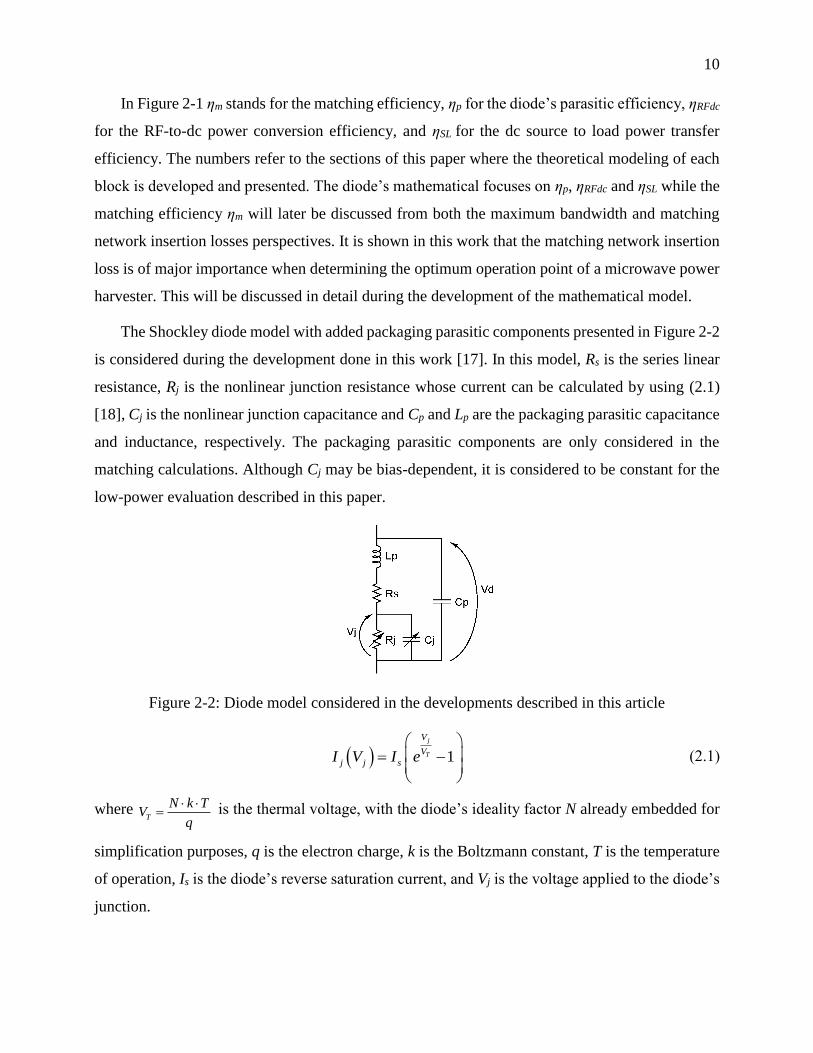
The Shockley diode model with added packaging parasitic components presented in Figure 2-2
is considered during the development done in this work [17]. In this model, Rs is the series linear
resistance, Rj is the nonlinear junction resistance whose current can be calculated by using (2.1)
[18], Cj is the nonlinear junction capacitance and Cp and Lp are the packaging parasitic capacitance
and inductance, respectively. The packaging parasitic components are only considered in the
matching calculations. Although Cj may be bias-dependent, it is considered to be constant for the
low-power evaluation described in this paper.
Figure 2-2: Diode model considered in the developments described in this article
1
j
T
V
V
jj sI V I e
(2.1)
where T
N k TV
q
is the thermal voltage, with the diode’s ideality factor N already embedded for
simplification purposes, q is the electron charge, k is the Boltzmann constant, T is the temperature
of operation, Is is the diode’s reverse saturation current, and Vj is the voltage applied to the diode’s
junction.

11
2.2.3 DC source-to-load power transfer efficiency
To evaluate the dc behavior, the diode junction can be modeled through the use of the Thévenin
or Norton equivalent circuits as shown in Figure 2-3.
In the Norton equivalent circuit, the total rectified current Ijdc is divided between the dc load
RL which is in series with the diode’s series resistance Rs, and the parallel diode’s junction
resistance Rj. The dc current at the load, Iload, can be calculated by the following equation:
0 0.
j load
load jf jdc jf
S j load L
R II V I V
R R I R
(2.2)
where Vjf0 is the excitation voltage over the diode’s junction at the fundamental frequency f0 and
Ijdc is the total dc current rectified by the diode junction.
DiodeDiode
VjDC
Rs
Rj
RL
Iload
Rs
Rj
RL
Iload
IjDC
(a) (b)
Figure 2-3: (a) Thévenin and (b) Norton equivalent circuits for the diode junction working as a dc
power supply.
The total dc power generated by the diode, Pdc, is calculated using Iload (2.2) and the resistive
loads at the dc current path. This can be calculated through the diode model given in Figure 2-2
and the series load RL, as given by circuit in Figure 2-3 (a).
2
0 .dc s j loaL d load jfP R R R I I V (2.3)
And the dc power delivered to the load, Pload, by:
2
0 .Lload load jfP R I V (2.4)
So the DC source-to-load power transfer efficiency can be calculated by:
( )d
load LSL
L s j loadc
P R
P R R R I
(2.5)

12
2.2.4 RF-to-dc power conversion efficiency
Most of the published RF and microwave power harvester models, which describe the RF-to-
dc power conversion efficiency, consider the diode as a perfect switch whose impedance
approaches RS, the diode’s series resistance when directly polarized, and infinity when reversely
polarized [17, 19]. This method delivers good results when the input signal is relatively large,
usually in the mW range and above, and the investigated diode has a high barrier leading to a large
zero-bias resistance (ZBR) Rj0. However, this method does not hold for very low input power
levels, or for low barrier diodes which present a small ZBR in the order of tens of kΩ and below.
As it may be seen in Figure 2-4 where the simulated junction resistance of the Skyworks SMS7630
[20] diode at -40 dBm is presented, the assumption that the diode works as a perfect switch is not
true anymore. In such a typical low power driving condition, the diode’s impedance varies between
2 kΩ and 20 kΩ over time, not reaching neither a 0 Ω neither an infinitely large impedance state.
Figure 2-4: Simulation result of the junction resistance of a SMS7630 diode, input power is -40
dBm and load is 5 kΩ. Rj is calculated using δV/δI.
To model this non-linearity of Rj, the zero bias current responsivity 0I will be used in this
work. The current responsivity (2.6) is defined as the ratio between the output dc current Ijdc and
the input RF power Pf0 [18] for a 0Ω load. The usual derivations of 0I however may only be used
in the diode’s square law region. Thus, an extended version of the current responsivity that will be
denoted by *
I and may be used out of the diode’s square-law region is proposed here.

13
0
j
I
DC
f
I
P (2.6)
To find its extended form, the diode’s I-V characteristic, given by (2.1) is extended in a Taylor
series. In a Taylor expansion around the 0 V point:
2
1 1 1.
1! 2! !
n
j
j j s
T
j j
T T
V V
V
VI V I
V n V
(2.7)
Assuming that the applied signal is a constant sinusoidal wave with fundamental frequency f0,
one can write Vj as
0 0 sin 2 ..j jfV V f t (2.8)
Substituting (2.8) into (2.7), and isolating only the terms in dc and in the fundamental
frequency, one can find the dc current generated at the junction, Ijdc, and the current at the
fundamental frequency, Ijf0. The power that reaches the diode junction at the fundamental
frequency, Pjf0, can then be found using equation (2.9).
0
1
0 0 0 0
0
2 4 62
0 0 0 0
.
1 1 1 12 8 192 9216
f
jf f j jf
jf jf jf jf
T T T T
P V f V I dt
V V V V
V V V V
(2.9)
Using Ijdc and casting (2.9) into (2.6), one can obtain the extended current responsivity, which
can be written as
00 0
2 4
0 0
*
0 2 4
0 0
1 11
16 5761
2 1 11
8 192
1 .
2 I I
jf jf
T T
I jf
T jf jf
T T
I
T
V V
V VV
V V V
V V
V
(2.10)
where 0I is the diode’s zero-bias current responsivity. This extended responsivity equation
results from the current-voltage relationship given in (2.1). What’s remarkable about (2.10) is that
the only diode intrinsic characteristic having an impact on the current responsivity is the diode’s

14
ideality factor N, embedded into VT.0I . This is inversely proportional to N and has a maximum
equal to 19.34 A/W at 300K. This is the maximum current responsivity that any Schottky diode
can reach at the ambient temperature, thereby standing for an important limitation in the use of
Schottky diodes for low power energy harvesters. A recently published microwave power rectifier
using heterojunction backward tunnel diodes with current responsivities in the order of 22 A/W
has demonstrated how such a technology can be used to break through this Schottky diode
limitation, thus greatly improving the microwave power harvester efficiency [10].
Equation (2.10) also depends upon the external parameter Vjf0. As the denominators from the
lower polynomial are smaller than the counterpart from the upper polynomial, *
I decreases when
Vjf0 increases, thus, when the input power increases. This decrease in responsivity can be
understood by looking at Figure 2-5 where the simulated SMS7630 current responsivity is given
together with two different amplitude Vj signals. The smaller amplitude signal remains in a
maximum I region. When the applied signal amplitude increases, the diode starts to operate in
regions with a reduced I . If one thinks of the total *
I as an average responsivity for the voltages
through which the junction is excited, the average would then decrease with the increasing
excitation amplitude. This variation of *
I as a function of the external excitation is represented by
in equation (2.10).
In order to calculate the total dc current generated at the diode junction Ijdc, equations (2.10)
and (2.6) are used for a given junction voltage Vjf0. The junction power Pjf0 is then found by using
(2.9) for this same value of Vjf0. This method can be used for low input power levels, ranging up to
few µW of input power. The model becomes less accurate for an increasing power because of the
simplification assumed in (2.8) where the harmonics and dc bias in the diode junction voltage were
ignored. This range, however, is enough for ambient microwave energy harvesting aplications and
can be extended as it will be further presented in section 2.2.8.
The presented equations can be used to calculate the total dc current generated by the diode
junction, Ijdc given the power arriving at the diode’s non-linear junction. In order to calculate the

15
total dc power delivered to the load, the effects of the dc source-to-load power transfer have to be
considered as shown in section 2.2.3.
Figure 2-5: Top part: Two sine waves, representing the voltage applied to the diode terminals.
Bottom part: Simulated current responsivity of the SMS7630 diode for a voltage sweep near the
zero-bias condition.
The total dc power generated by the diode, Pdc, can then be calculated using Iload (2.2) and the
equivalent resistance at the dc current path. This can be calculated using the Thévenin equivalent
circuit in which the diode is in series with the load, as described by (2.3). Defining the RF-to-dc
power conversion efficiency as the total dc generated power divided by the power that reaches the
junction, one can write the following,
0 0
22
0
0
( ). . .
( ) I
j loadDCRFdc I jf
jf L s j load
R IPP
P R R R I
(2.11)
Equations (2.5) and (2.11) may be used to determine the optimum load value with which the
maximum efficiency in the RF-to-dc power conversion efficiency is reached. In Annex A, it is
shown that the load value for which the maximum efficiency is obtained is equal to Rs+Rj(Iload).
This can be simplified to Rj(Iload) within the square-law operation limits as Rs is much smaller than
Rj(Iload).

16
2.2.5 Parasitic Efficiency
Due to the low-pass filter effect of the diode’s junction capacitance Cj0, some of the RF current
that reaches the diode is shunted, therefore dissipating power in the series resistance Rs. The total
RF power that is delivered to the diode may be calculated by adding the power that reaches its
junction (2.9) to the power that is dissipated by the diode’s series resistance Rs. The later may be
calculated using equation (2.12), which can be derived by using simple linear circuit theory.
2
0
0 0 0
0
1 . 2. .2. . . .
2s
jf
R s j jf
jf
PP R j f C V
V (2.12)
The parasitic efficiency can be defined as the ratio between the total power supplied to the
diode and the power that reaches the nonlinear junction, which may be expressed by
0
0 s
jf
parasitics
jf R
P
P P
(2.13)
Equations (2.12) and (2.13) can be simplified for the square-law region, where the junction
resistance is considered to be constant and equal to Rj0, the resulting equation is given in (2.14) and
was already given in [9, 18].
2
2
0 0 01
1
2parasi
j j
ti s
s
c
f C R R
(2.14)
Equations (2.5), (2.11) and (2.13), which are used to calculate ηSL, ηRFdc and ηparasitics respectively,
describe the power conversion efficiencies related to the diode parasitic components and non-
linearity. Assuming that the optimum load is chosen such that RFDC SL is maximized, one can
assume from equation (2.11) that diodes with higher Rj will reach higher efficiencies. In equation
(2.14), however, the impact of a higher Rj0 is seen to decrease efficiency. Finally, as it will be
shown subsequently, the zero bias resistance value also plays a key role in the matching network
losses. Those three tendencies will be analysed in the next session and the matching network
insertion losses impact on the total rectifier PCE is evaluated in detail.
2.2.6 Matching Efficiency
The matching network insertion loss, or in turn, matching efficiency ηm, plays a significant role
when determining the optimum diode for an ambient microwave power harvester. While (2.11)

17
indicates that a diode with a high Rj0 is expected to deliver a higher RF-to-dc power conversion
efficiency, it is shown that ηm is inversely proportional to Rj0. Using the given model, an optimum
Rj0 where ηm•ηRFdc•ηSL is maximized can be suggested, indicating the optimum diode’s zero-bias
junction resistance.
A prior knowledge of the matching network technology in terms of transmission line
attenuation and propagation constants as well as lumped components quality factors, can be used
to estimate the matching efficiency ηm as follows [21],
1
1m
r
m
Q
Q
(2.15)
1HIGHr
LOW
RQ
R (2.16)
where RHIGH and RLOW are the highest and lowest real impedances chosen from the source or the
load, being typically the source impedance and Rj, respectively, when matching a diode. Qr is
called the required quality factor while Qm is the matching network quality factor that is actually
obtained.
Finding the value of Qm can be simplified by approximating the diode by a parallel Rd//Cd
circuit at the operation point of interest, which is determined by the input power and f0. In this case,
Rd is the equivalent parallel diode resistance to which the power is delivered and the equivalent
parallel capacitance Cd will be absorbed into the matching network losses and bandwidth
calculations. For a center frequency of interest, Rd and Cd may be calculated using the equations
below, while maintaining the equivalent load quality factor [21]:
2Re[ ] (1 )d diode diodeR Z Q (2.17)
2
0
Im[ ](1 )
2
dioded diode
ZC Q
f
(2.18)
where Zdiode is the input impedance of the diode alone at f0 and the input power level of interest,
and Qdiode is the quality factor of the diode, calculated at the same frequency and power. For
frequencies far below the diode cut-off frequency, it can be approximated by:
Im[ ]
Re[ ]
diodediode
diode
ZQ
Z (2.19)

18
To obtain the quality factor of the matching network, its input impedance as a function of
frequency Zmatch(f) needs to be calculated, with the first component of the matching network being
Cd. Once this equation is known, Qm may be calculated using one of the two equations below [22]:
Im[ ( )]Im[ ( )]
1( )
2 Re[ ( )]
matchmatch
m
match
d Y fY f f
dfQ f
Y f
(2.20)
Im[ ( )]Im[ ( )]
1( )
2 Re[ ( )]
matchmatch
m
match
d Z fZ f f
dfQ f
Z f
(2.21)
where Ymatch(f) is the input admittance of the matching network, given by 1/Zmatch(f). Equation
(2.20) is used when the matching network behaves as a parallel resonator near f0, while equation
(2.21) is used when the behaviour resembles a series resonator.
Every component used in the matching network’s Zmatch(f) calculation needs to have its
contributing parasitic parts included. When transmission line distributed components are used, the
complex characteristic impedance of the line Zc needs to be used. In [23], for example, it is shown
that the quality factor of a short stub can vary by a factor of 2 if a simplified real impedance is used
instead of the complex impedance of the transmission line.
When transmission lines are used as components of the matching network, it is important to
take into account the effect that the standing waves have on losses. The increased voltage and
current that appear on the line would introduce higher losses to the system. In [24], it is shown that
an equivalent transmission line attenuation constant αr can be calculated, which will account for
these increased losses. αr is related to the matched transmission line attenuation constant αm by the
following equation:
2 1
2r m
r
r
(2.22)
where r is the standing wave ratio sustained by the transmission line, which is usually calculated
using (2.23), where ΓL is the reflection coefficient at the load side.
1
1
L
L
r
(2.23)
However, since transmission lines used in the design of matching networks are usually shorter
than half-wavelength, it is not possible to assume that both maximum and minimum current and

19
voltage nodes will appear in the standing wave sustained in the transmission line under
consideration. For this reason, equation (2.23) cannot be used.
Zs Zc ZL
Γ1 Γ2 Γ3
Vin
l z0
Figure 2-6: Travelling wave approach used to calculate the standing wave ratio in a transmission
line of length l.
Using the travelling wave formulation, one can calculate the voltage at a short length of
transmission line with reflection at both ends. Assuming a transmission line with propagation
constant γ, characteristic impedance Zc and length l, connected to a source with impedance ZS and
a load with impedance ZL, as shown in Figure 2-6, one can write the voltage on the transmission
line Vl as a function of the position z as given by equation (2.24).
2 2
3 2 3
2 4 2 2 4
2 3 2 3
...( )
...
z l z l z
l in l z l z
e e e e eV z V
e e e e
(2.24)
which can then be simplified to (2.26) by using (2.25).
0
1
1
n
n
xx
for |x| < 1 (2.25)
2
3
2
2 3
( )1
z z l
l in l
e e eV z V
e
(2.26)
Using the points where the first derivative of (2.26) with respect to z equals 0, one can find the
positions where |Vl(z)| has a maximum or a minimum point. In Annex B, it is shown that this
happens for:
atan( / )
2
n D Cz
(2.27)
where 2
3 ( )le C Di , β is the transmission line’s phase constant and n is an integer equal or
greater than 0.

20
If a z value is found to be within the limits of the transmission line length, a standing voltage
maximum or minimum is found at this position. For short transmission lines, the maximum and
minimums must also be verified at the transmission line ends when less than two valid values of z
are obtained from equation (2.27). Having the maximum and minimum standing wave voltages
that occur within the transmission line boundaries, equation (2.28) is used to calculate the
maximum to minimum voltage ratio found in the transmission line.
max
min
( )
( )
l
l
V zr
V z (2.28)
This value of r is used in conjunction with (2.22) to calculate the equivalent attenuation
constant αr for the transmission line, which is used to construct the Zmatch(f) matching network input
impedance equation.
Adding the matching network insertion loss effects to the microwave power rectification model
creates a model where the total trade-off between the diode’s junction resistance and the maximum
microwave power rectification efficiency can be studied.
Such a tradeoff is shown in the bottom graph depicted in Figure 2-7 for an input power equal
to -30 dBm, using a hypothetical parasitic-less diode. The rectifier power conversion efficiencies
and insertion losses are calculated by considering that a microstrip L-Matching network is used,
which is composed by a series transmission line and a parallel short-circuited stub, which lengths
are optimized to minimize reflections for every new value of Rj. Low loss Rogers RT/Duroid 6002
substrate with 30 mil thickness and 18 µm copper cladding is used for the matching network
insertion losses calculations. The microstrip line is 76 mil wide and the transmission line’s
propagation constant and complex characteristic impedance functions are extracted by using the
method proposed in [25]. This evaluation provides the range of junction resistances where the
highest rectification efficiencies can be obtained by using the proposed matching network. It is
clear from this graph that for a parasitic-less diode, a maximum could be obtained near 17kΩ,
however close-to-the maximum efficiencies could be achieved with diodes that have an Rj0 ranging
from 5kΩ up to 50kΩ. The parasitic components will later reduce the maximum efficiency and
play an important role in the maximum bandwidth that can be matched to the diode. This will be
shown in the next section.

21
Figure 2-7: Top: Calculated required quality factor Qr and obtained matching network quality
factor Qm. Bottom: Calculated matching network efficiency, diode’s 𝞰RFdc∙𝞰SL and total
efficiency at -30 dBm 1.95GHz. Load value equal to Rj.
2.2.7 Maximum Bandwidth
The relationship between the load impedance and the maximum attainable matching bandwidth
was described by Bode [26] and Fano [27], being known as the Bode-Fano criteria [28]. It gives
the maximum bandwidth that can be matched to a load, given the load’s equivalent circuit and the
maximum desired reflection coefficient.
Equation (2.29) can be used to calculate ∆B, the maximum obtainable fractional bandwidth. It
is derived using the Bode-Fano criterion for a parallel RC circuit.
0
1.
12lnd d
inband
BR f C
(2.29)
where f0 is the frequency of interest, corresponding to the central frequency of the band, and Γinband
is the desired reflection coefficient.
It is important to bear in mind that this equation is derived by assuming that the reflection
coefficient is flat and equal to |Γinband| for the matched band, and equal to one outside of this band.

22
In this derivation, there are also other implicit assumptions, namely the availability of lossless
matching networks and wideband lossless impedance transformers. As one knows, matching
networks always introduce losses to the system, and wideband impedance transformers are difficult
to obtain over microwave frequency range for very different source and load impedances.
This means that in a real circuit design scenario, the maximum attainable bandwidth is actually
lower than the calculated by the Bode-Fano criteria, as such sharp transitions and flat passband are
impossible to obtain. The out of band reflection coefficient will also not be equal to one for the
whole frequency spectrum, thus reducing even more the maximum bandwidth that may be obtained
for the passband.
However, the Bode-Fano criteria can be used to establish an upper bound to the maximum
bandwidth that can be matched to a diode at a given frequency and estimated input power. It will
be shown that, despite that high Rj0 diodes show an increased ηRFdc at low power level according
to (2.11), the maximum bandwidth that can be matched to them is usually very narrow.
2.2.8 Extension of the Low Power Model
The aforementioned method can be used to evaluate the RF-to-dc power conversion
mechanism and understand where the power conversion inefficiencies originate. Even though
equations (2.7) to (2.10) are limited in power to a few µW, this analysis can be extended to a larger
power range by means of pre-generated Vj0 as function of the junction power and load resistor
Vj0(Pjf0,Rl), and current responsivity delta as function of the junction voltage and normalized load
0I (Vj0, Rl/Rj0) matrixes, which are calculated with the aid of an Harmonic Balance algorithm
implemented in MATLAB [29]. The 0I
matrix contours are given in Figure 2-8. These may be
used for Schottky diodes operating below the breakdown voltage, however, the Vj0 contours which
are shown in Figure 2-9 are diode dependent and need to be obtained for each different diode to be
evaluated in higher input powers. All inductive and capacitive parasitic elements are removed
during the contours generation to make them frequency independent. In this way, any further
analysis may be done quickly and the results may be extrapolated to any frequency using only the
previously presented linear equations. This procedure can be used to quickly evaluate and optimize
microwave rectifiers at different frequencies or evaluate different matching network topologies.
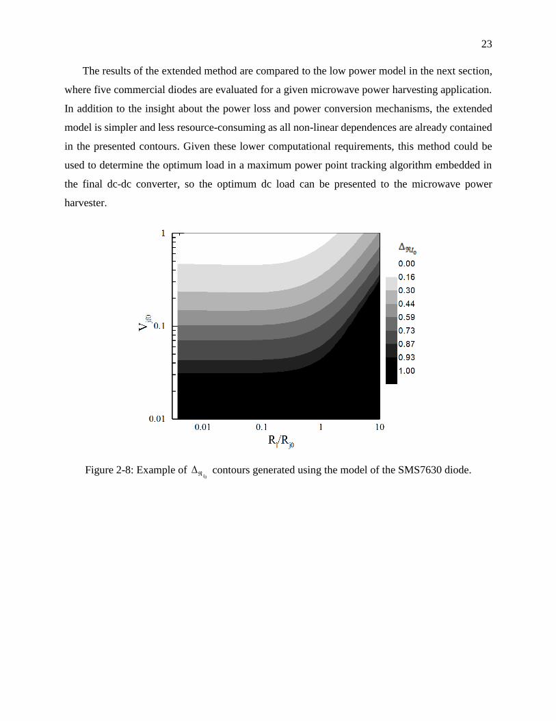
23
The results of the extended method are compared to the low power model in the next section,
where five commercial diodes are evaluated for a given microwave power harvesting application.
In addition to the insight about the power loss and power conversion mechanisms, the extended
model is simpler and less resource-consuming as all non-linear dependences are already contained
in the presented contours. Given these lower computational requirements, this method could be
used to determine the optimum load in a maximum power point tracking algorithm embedded in
the final dc-dc converter, so the optimum dc load can be presented to the microwave power
harvester.
Figure 2-8: Example of 0I
contours generated using the model of the SMS7630 diode.
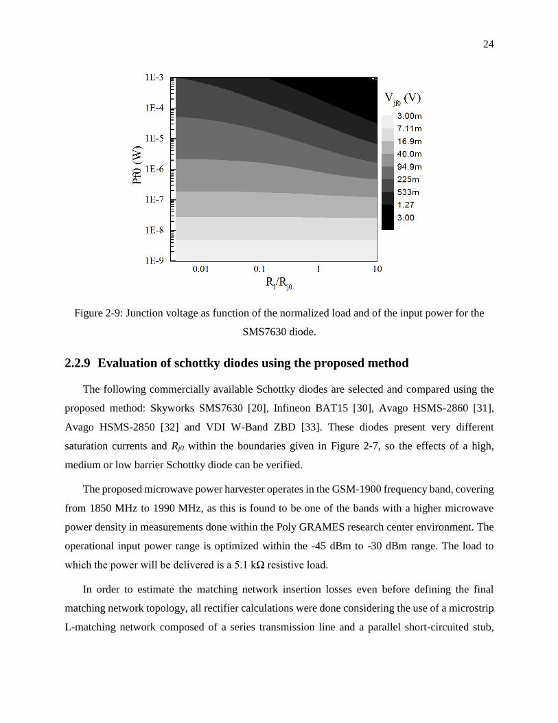
24
Figure 2-9: Junction voltage as function of the normalized load and of the input power for the
SMS7630 diode.
2.2.9 Evaluation of schottky diodes using the proposed method
The following commercially available Schottky diodes are selected and compared using the
proposed method: Skyworks SMS7630 [20], Infineon BAT15 [30], Avago HSMS-2860 [31],
Avago HSMS-2850 [32] and VDI W-Band ZBD [33]. These diodes present very different
saturation currents and Rj0 within the boundaries given in Figure 2-7, so the effects of a high,
medium or low barrier Schottky diode can be verified.
The proposed microwave power harvester operates in the GSM-1900 frequency band, covering
from 1850 MHz to 1990 MHz, as this is found to be one of the bands with a higher microwave
power density in measurements done within the Poly GRAMES research center environment. The
operational input power range is optimized within the -45 dBm to -30 dBm range. The load to
which the power will be delivered is a 5.1 kΩ resistive load.
In order to estimate the matching network insertion losses even before defining the final
matching network topology, all rectifier calculations were done considering the use of a microstrip
L-matching network composed of a series transmission line and a parallel short-circuited stub,

25
which is also used as the dc current path. The same substrate and line impedances presented in the
previous section that discussed the matching network insertion losses estimation model are used.
Using the proposed method and the diodes’ characteristics given in the datasheets, the total
RF-to-dc power conversion efficiency and the losses that take place in this conversion have been
estimated. The result is given in Figure 2-10 for the five proposed diodes. The results are organized
from the diode with the highest Rj0 on the top, to the lowest Rj0 at the bottom. The stacked areas
are calculated with the extended model, using the pre-generated Vj0(Pjf0,Rl) and 0I
(Vj0, Rl/Rj0)
matrices. The red triangles correspond to the low power model, while the blue squares make use
of an extended version of the low power model that does not need the deviation matrices. In this
case, IL is calculated as the average of (2.2) and (2.30). This last method is found empirically and
extends the range of power levels in which the low power model may be used up to nearly -20
dBm.
0
0 0
0
.j
load jf jDC jf
S j l
RI V I V
R R R
(2.30)
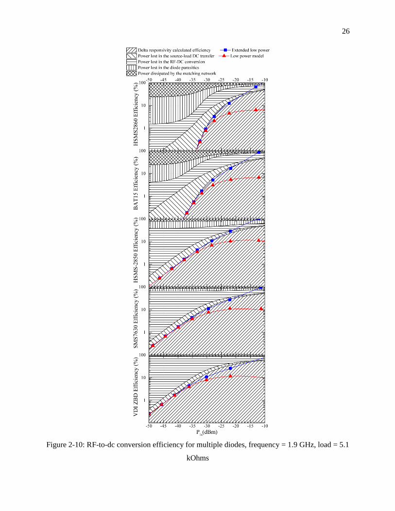
26
Figure 2-10: RF-to-dc conversion efficiency for multiple diodes, frequency = 1.9 GHz, load = 5.1
kOhms
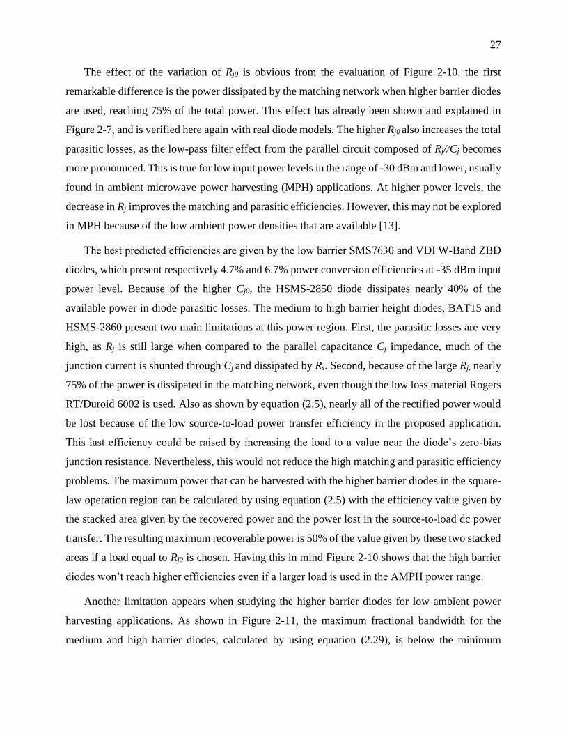
27
The effect of the variation of Rj0 is obvious from the evaluation of Figure 2-10, the first
remarkable difference is the power dissipated by the matching network when higher barrier diodes
are used, reaching 75% of the total power. This effect has already been shown and explained in
Figure 2-7, and is verified here again with real diode models. The higher Rj0 also increases the total
parasitic losses, as the low-pass filter effect from the parallel circuit composed of Rj//Cj becomes
more pronounced. This is true for low input power levels in the range of -30 dBm and lower, usually
found in ambient microwave power harvesting (MPH) applications. At higher power levels, the
decrease in Rj improves the matching and parasitic efficiencies. However, this may not be explored
in MPH because of the low ambient power densities that are available [13].
The best predicted efficiencies are given by the low barrier SMS7630 and VDI W-Band ZBD
diodes, which present respectively 4.7% and 6.7% power conversion efficiencies at -35 dBm input
power level. Because of the higher Cj0, the HSMS-2850 diode dissipates nearly 40% of the
available power in diode parasitic losses. The medium to high barrier height diodes, BAT15 and
HSMS-2860 present two main limitations at this power region. First, the parasitic losses are very
high, as Rj is still large when compared to the parallel capacitance Cj impedance, much of the
junction current is shunted through Cj and dissipated by Rs. Second, because of the large Rj, nearly
75% of the power is dissipated in the matching network, even though the low loss material Rogers
RT/Duroid 6002 is used. Also as shown by equation (2.5), nearly all of the rectified power would
be lost because of the low source-to-load power transfer efficiency in the proposed application.
This last efficiency could be raised by increasing the load to a value near the diode’s zero-bias
junction resistance. Nevertheless, this would not reduce the high matching and parasitic efficiency
problems. The maximum power that can be harvested with the higher barrier diodes in the square-
law operation region can be calculated by using equation (2.5) with the efficiency value given by
the stacked area given by the recovered power and the power lost in the source-to-load dc power
transfer. The resulting maximum recoverable power is 50% of the value given by these two stacked
areas if a load equal to Rj0 is chosen. Having this in mind Figure 2-10 shows that the high barrier
diodes won’t reach higher efficiencies even if a larger load is used in the AMPH power range.
Another limitation appears when studying the higher barrier diodes for low ambient power
harvesting applications. As shown in Figure 2-11, the maximum fractional bandwidth for the
medium and high barrier diodes, calculated by using equation (2.29), is below the minimum
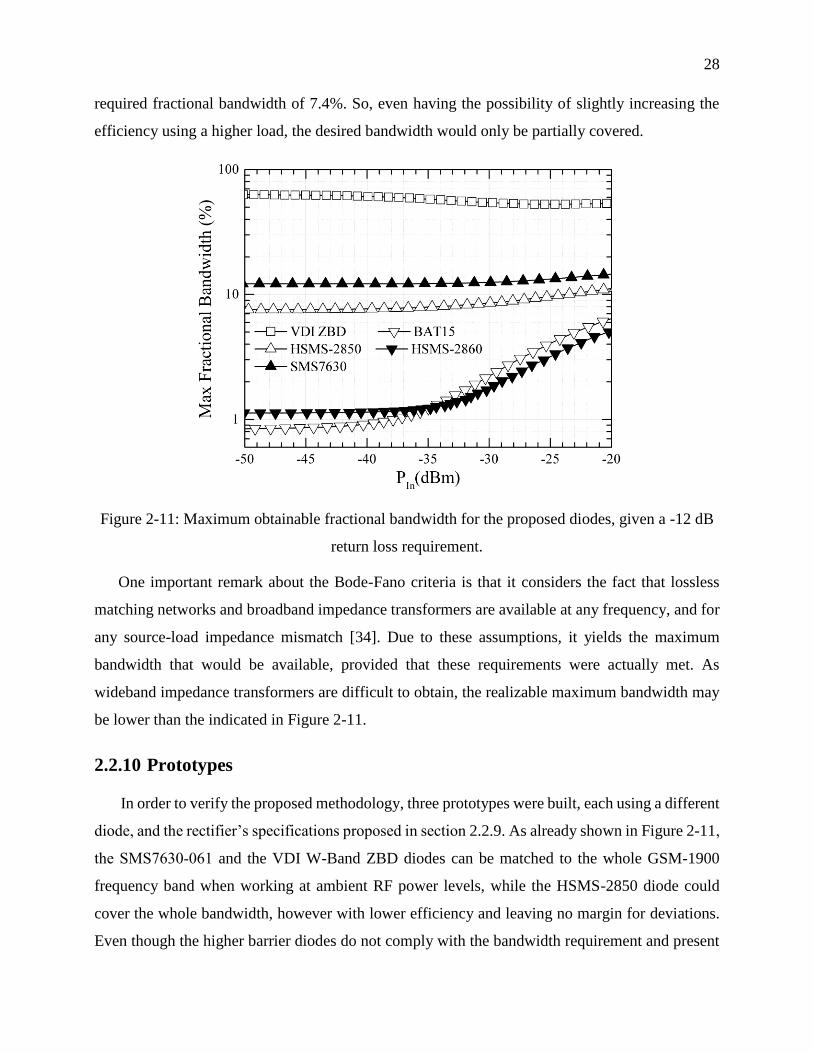
28
required fractional bandwidth of 7.4%. So, even having the possibility of slightly increasing the
efficiency using a higher load, the desired bandwidth would only be partially covered.
Figure 2-11: Maximum obtainable fractional bandwidth for the proposed diodes, given a -12 dB
return loss requirement.
One important remark about the Bode-Fano criteria is that it considers the fact that lossless
matching networks and broadband impedance transformers are available at any frequency, and for
any source-load impedance mismatch [34]. Due to these assumptions, it yields the maximum
bandwidth that would be available, provided that these requirements were actually met. As
wideband impedance transformers are difficult to obtain, the realizable maximum bandwidth may
be lower than the indicated in Figure 2-11.
2.2.10 Prototypes
In order to verify the proposed methodology, three prototypes were built, each using a different
diode, and the rectifier’s specifications proposed in section 2.2.9. As already shown in Figure 2-11,
the SMS7630-061 and the VDI W-Band ZBD diodes can be matched to the whole GSM-1900
frequency band when working at ambient RF power levels, while the HSMS-2850 diode could
cover the whole bandwidth, however with lower efficiency and leaving no margin for deviations.
Even though the higher barrier diodes do not comply with the bandwidth requirement and present

29
lower RF-to-dc power conversion efficiency due to high matching network insertion losses, a third
prototype using the BAT15 diode is presented in order to verify the model’s predictions. The
methodology used in this work to build the prototypes is described hereunder.
1st: The diode’s input impedance is calculated using the diode datasheet information and, when
available, SPICE model parameters. The input power used during the matching circuit development
is -35 dBm and the load is 5.1 kΩ.
2nd: An initial matching network, covering at least the frequency band ranging from 1.84 GHz
to 1.99 GHz is generated using the Simplified Real Frequency Technique (SRFT) [35, 36]. The
minimum desired return loss is 12 dB.
3rd: The lumped components matching networks are converted into mixed matching networks,
both lumped and distributed components are optimized afterwards using Keysight ADS LSSP and
Momentum co-simulation.
The prototypes are then built using microstrip technology over a 30 mil Rogers RT/Duroid
6002 substrate, the same substrate is used in the model calculations given in Figure 2-10. A picture
of the circuits is shown in Figure 2-13.
For the efficiency measurement, the output of a RF generator is calibrated and then connected
to the prototypes. The dc voltage Vdc over the output 5.1 kΩ load resistor is measured by a HP
34401A precision voltmeter. With the voltage values in hand, the measured total efficiency is
calculated using equation (2.31).
2
.
dcmeas
l in
V
R P (2.31)
The simulated and measured S11 for a -35 dBm input signal, as well as the measured and
calculated power conversion efficiency for a -30 dBm input signal, are shown in Figure 2-12.
The maximum bandwidth for a -12 dB return loss, calculated using the Bode-Fano criteria, is
shown as a grayed out area for the SMS7630 and BAT15 diodes. The obtained bandwidths are
near-to-the maximum predicted value, considering that the measured return loss is lower than -12
dB for some frequencies, and not flat as considered in the Bode-Fano criteria derivations.

30
Figure 2-12: Measured and calculated S11 (at -35 dBm) and power conversion efficiency (at -30
dbm). The theoretical maximum bandwidth for -12 dB return loss is indicated by the grayed out
area. The proposed prototipes bandwidth is indicated by the parallel blue line.

31
Figure 2-13: Picture of the circuits built for this paper. Top: SMS7630. Middle: VDI ZBD.
Bottom: BAT15.
As shown in the results, the agreement between the simulated and measured S11 is very good
for the SMS7630 and BAT15 diodes. However, a difference is observed between the initially
simulated and measured S11 values for the VDI prototype. This happened mainly because of a
large tolerance that this diode presents for the value of Is, reflecting on a junction resistance that
may vary from 2.5 kΩ to 6 kΩ. It was initially assumed in this work an Is value equal to 11 𝛍A;
however from the measurements it was found that the used sample presents an Is near to 7 𝛍A. The
measured S11 values presented in Figure 2-12 are obtained after tuning the matching network,
which was done by using a copper tape as can be seen in Figure 2-13.
The measured power conversion efficiencies agree very well with the predicted values, which
are calculated using the 0I
extended mathematical model. ηm is calculated using the measured
reflection coefficient and the matching network insertion loss, estimated using Keysight ADS

32
Momentum software package, as the wider band matching networks become too complicated to be
modeled mathematically.
After the bandwidth measurement, a power sweep is done to verify the model power
conversion efficiency prediction at different power levels. The power distribution, calculated using
the 0I
mathematical model and simulated matching network insertion loss is shown in Figure
2-14 for the three built prototypes, together with the measured results. A very good agreement
between the model predictions and measurements is found and verified for the BAT15 and VDI
prototypes. A small difference is observed between the measured and predicted power conversion
efficiencies of the SMS7630, this difference shown in Figure 2-12 and Figure 2-14 is believed to
be the result of an underestimation of the used diode model parasitic components, or in the diode
package parasitic components.
As expected from the previous discussions, the higher initial mismatch between source and
load for the diodes with higher Rj0 results in a very high loss of Pin in connection with the increased
matching network insertion losses. For the SMS7630 diode, this loss accounts for 18% of Pin, while
for the BAT15 diode this raises to nearly 82% of Pin. The increase in the matching network insertion
losses for the BAT15 prototype, when compared to the predictions given inFigure 2-10, is mainly
caused by the use of a longer transmission line between the diode and the parallel capacitor, when
compared to the transmission line used with a parallel shorted stub solution, which allows a larger
standing wave ratio to be sustained increasing losses.
Despite the fact that the SMS7630 diode has a slightly higher Rj than the VDI ZBD diode, the
larger diode parasitic losses decrease the final efficiency, as nearly 18.8% of the total input power
is lost in the diode’s parasitic components. This results in a total efficiency very near for both
rectifiers, with the VDI ZBD rectifier delivering the best performance, reaching 11.29% at -30
dBm compared to 8.08% measured on the SMS7630 rectifier.
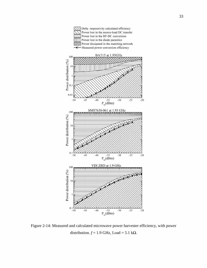
33
Figure 2-14: Measured and calculated microwave power harvester efficiency, with power
distribution. f = 1.9 GHz, Load = 5.1 kΩ.
34
2.2.11 Conclusion
In this paper, a mathematical model has been presented and verified, in which the power
conversion efficiency-related physical mechanisms of microwave power harvesters using Schottky
diodes are explained and formulated. Knowing where the power is dissipated enables the design
and development of a new class of rectifiers with maximized conversion efficiency. The modeled
efficiencies, calculated in conjunction with the matching network losses, are in a close agreement
with the measured results. Even though the matching network insertion losses are approximated by
a simpler L-matching network, the results show a good agreement with the final wider band
matching network calculated and measured results, thus substantiating the claim that the proposed
model can be used as a trustworthy approximation of the maximum attainable power conversion
efficiencies, even before having the rectifier circuit designed.
Figure 2-15 shows a comparison between the three proposed models: the low power model
presented in the beginning of this paper, the extended low power model using (2.30) and the delta-
responsivity matrix model described in item 2.2.8. The matching efficiency was removed to
compare the proposed models to previously published mathematical models, so the power ranges
and scenarios where each method delivers the best results could be highlighted, these models are:
the diode operating as a switch [19], and the Ritz-Galerkin solution for the diode non-linear
equations [37]. The Keysight ADS Harmonic Balance result was added as reference. Since the
Ritz-Galerkin model uses a given source voltage and impedance instead of the power arriving at
the diode to calculate the output dc voltage and power, the reflection coefficient at the source-diode
interface is used to calculate the power delivered to the diode and hence the power conversion
efficiency. This reflection coefficient has to be pre-generated using a harmonic balance, as the non-
linear diode input impedance is unknown.
The limitation in the low power models for higher input powers is evident from Figure 2-15.
Nevertheless, the result at input power levels up to few microwatts makes the low power and the
extended low power models very good tools to predict the performance of ambient microwave
power harvesters. The delta-responsivity matrix model delivers an exact result when compared to
the Keysight ADS simulation results, even at higher input power levels. The Ritz-Galerkin model
has a shift up in the efficiency for the SMS7630 and the BAT15 diodes, as the result of a
simplification in the model derivation where the parasitic capacitances are ignored, this effect is
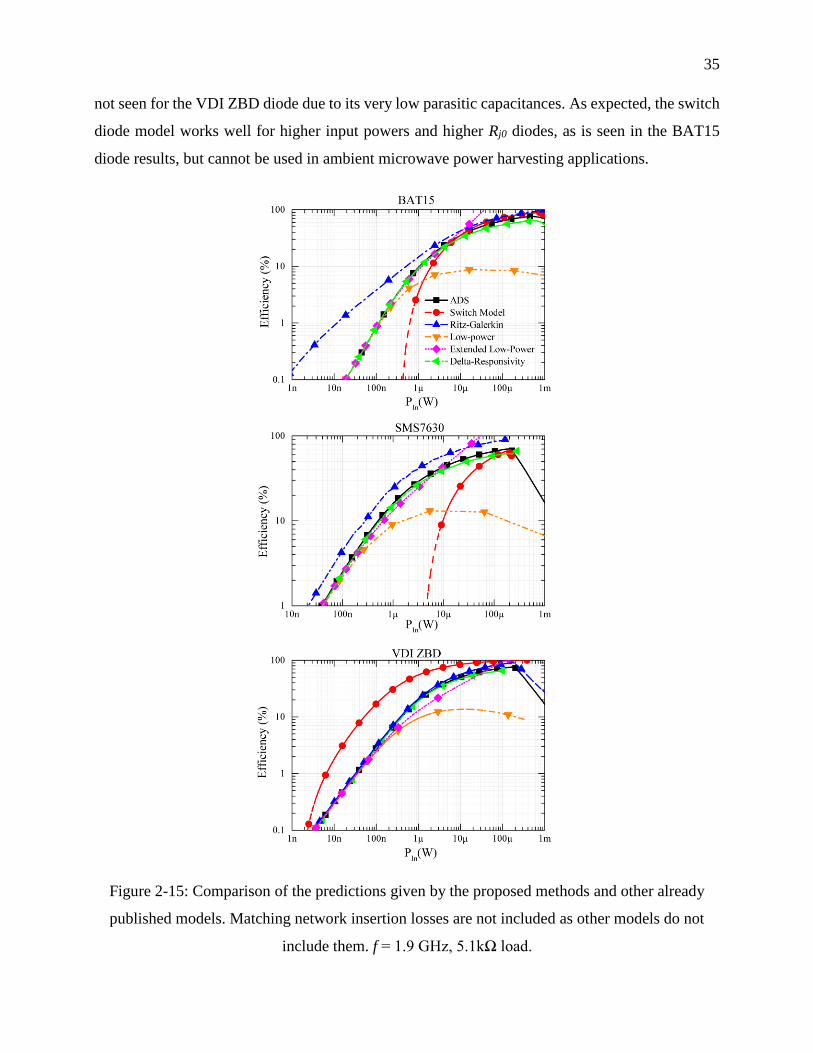
35
not seen for the VDI ZBD diode due to its very low parasitic capacitances. As expected, the switch
diode model works well for higher input powers and higher Rj0 diodes, as is seen in the BAT15
diode results, but cannot be used in ambient microwave power harvesting applications.
Figure 2-15: Comparison of the predictions given by the proposed methods and other already
published models. Matching network insertion losses are not included as other models do not
include them. f = 1.9 GHz, 5.1kΩ load.
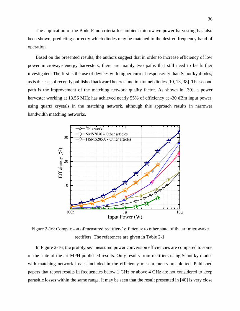
36
The application of the Bode-Fano criteria for ambient microwave power harvesting has also
been shown, predicting correctly which diodes may be matched to the desired frequency band of
operation.
Based on the presented results, the authors suggest that in order to increase efficiency of low
power microwave energy harvesters, there are mainly two paths that still need to be further
investigated. The first is the use of devices with higher current responsivity than Schottky diodes,
as is the case of recently published backward hetero-junction tunnel diodes [10, 13, 38]. The second
path is the improvement of the matching network quality factor. As shown in [39], a power
harvester working at 13.56 MHz has achieved nearly 55% of efficiency at -30 dBm input power,
using quartz crystals in the matching network, although this approach results in narrower
bandwidth matching networks.
Figure 2-16: Comparison of measured rectifiers’ efficiency to other state of the art microwave
rectifiers. The references are given in Table 2-1.
In Figure 2-16, the prototypes’ measured power conversion efficiencies are compared to some
of the state-of-the-art MPH published results. Only results from rectifiers using Schottky diodes
with matching network losses included in the efficiency measurements are plotted. Published
papers that report results in frequencies below 1 GHz or above 4 GHz are not considered to keep
parasitic losses within the same range. It may be seen that the result presented in [40] is very close

37
to the performance obtained by the prototype using the SMS7630 diode. This is expected as the
load value is near and both diodes present similar characteristics. As far as the authors are aware,
the efficiency presented by the prototype using the VDI ZBD diode is the highest published within
the power range of interest using Schottky diodes for rectification, being close to the latest results
presented for CMOS rectifiers [41] at the 1.9GHz frequency range.
Table 2-1: List of Rectifiers Presented in Figure 2-16
Symbol Year Diode Frequency Reference
2015 VDI ZBD 1.9 GHz Prototype
2015 SMS7630 1.9 GHz Prototype
2015 BAT15 1.9 GHZ Prototype
2010 SMS7630 2.45 GHz [42]
2014 SMS7630 2.45 GHz [43]
2013 HSMS2855 2.45 GHz [44]
2012 HSMS285X 1.8 GHz [45]
2014 HSMS285X 1.8 GHz [40]
2014 HSMS285X 2.1 GHz [40]
2.2.12 Acknowledgment
The authors would like to acknowledge the financial support of the Natural Sciences and
Engineering Research Council of Canada (NSERC) and CREATE PERSWADE Training Program,
which have partially funded the work presented in this paper. Also the samples provided by Rogers
Corporation and Virginia Diodes are deeply appreciated, and were of great importance during the
development of the presented work.
The authors wish to thank J. Gauthier, D. Dousset, M. Thibault, S. Dubé, T. Antonescu, and J.-S.
Décarie of the Poly-Grames Research Center, Ecole Polytechnique de Montreal, for their technical
assistance.
2.2.13 Appendix A
The mathematical proof of the optimum load where the maximum PCE is obtained is shown
below, this is valid for the low input power range explored in this work, usually while the diode is
operating in the square-law region. From (2.5) and (2.11) one can write:

38
2
2
L j
SL RFdc
L S j
K R R
R R R
(2.32)
where 0
2
0 0II jfK P . The first derivative of this equation as a function of the load RL is
shown below:
2 2
2
2( ) j L S j L jSL RFdc
L L S j
K R R R R K R R
R R R R
(2.33)
Making it equal to 0, one can find the values of RL where 𝞰SL𝞰RFdc has a maximum or a
minimum:
2 2
2 3 2
2 0j L S j L j
j S j L j
K R R R R K R R
R R R R R
L S jR R R (2.34)
As the second derivative of 𝞰SL∙ 𝞰RFdc is always negative, this point represents the only
maximum of 𝞰SL∙ 𝞰RFdc, which happens when the load is equal to the diode resistance (which can
be approximated by Rj at low power level).
2.2.14 Appendix B
In order to find the z positions where (26) has a minimum voltage amplitude or a maximum
voltage amplitude, its first derivative is calculated by
2
3
2
2 3
( )
1
z z l
l in
l
e e eV z V
z e z
(2.35)
Making 2
3
lC iD e to simplify the mathematical derivation:
2
2 3
( )
1
z z
l in
l
e C iD eV z V
z e z
(2.36)
One can use the points where this equation is equal to zero so to find the candidate maximum
and minimum standing wave voltage amplitude positions:

39
z ze C iD e
z
2
1 cos sinC z D z
z
2
cos 1 sin0
D z C z
z
(2.37)
Expanding these equations and simplifying the resulting expression using trigonometric
identities one can get:
sin 2 cos 2 0C z D z (2.38)
which finally results in the previously given result equal to:
n +atan
2
DC
z
(2.39)
where n is any integer number equal or larger than zero.
40
CHAPITRE 3 RÉCUPÉRATION HYBRIDE COOPÉRATIVE
D’ÉNERGIE AMBIANTE
3.1 Introduction
L’un des principaux obstacles à surmonter pour que la récupération d’énergie ambiante
devienne une technologie utilisable dans les applications commerciales est la faible efficacité de
conversion de la puissance reçue en courant-continu, qui ne permet pas de maximiser la puissance
totale récupérée. L’état de l’art des circuits de REMA présentait des efficacités de conversion
proches de 5% jusqu’à la publication de ce travail pour une puissance à l’entrée proche de -30 dBm
et une fréquence dans la bande allant de 1 GHz - 3 GHz, comme montré dans la Figure 2-16. Cette
efficacité amène à une puissance rectifiée proche de 50 nW, tout en admettant qu’une puissance
continue (CW) est fournie à l’entrée du circuit de REMA, ce qui n’est pas toujours vrai dans un
scénario réel, où les signaux vont plutôt présenter une amplitude variable et/ou être intermittents.
La récupération d’énergie ambiante provenant d’autres sources, comme la vibration mécanique,
souffre aussi d’une limitation semblable quand la puissance captée de l’environnement est très
faible.
Selon le modèle mathématique présenté dans le chapitre 2, l’efficacité de la conversion de
puissance RF-en-cc effectué dans une jonction non linéaire est proportionnelle à la puissance
fournie à cette même jonction. Ce résultat est donné par l’équation (2-11), copiée ci-dessous :
0 0
22
0
0
( ). . .
( ) I
j loaddcRFdc I jf
jf L s j load
R IPP
P R R R I
(3.1)
Selon cette équation, l’augmentation de la puissance Pjf0 fournie à la résistance de jonction
devrait se traduire par une augmentation de la puissance rectifiée Pdc, et ce, de manière quadratique
en raison d’une augmentation de l’efficacité ηRFcc. Soit :
0 0
22 2
00
( ).
( ) I
j load
DC RFdc I f M
L s j l d
jf P
oa
R IP P
R R RP
I
(3.2)
Cependant, vu que les sources distribuées dans le milieu ambiante ne sont pas connues ni
contrôlées, la puissance micro-ondes disponible ne peux pas être modifiée pour les applications de
REMA. Toutefois, il est néanmoins possible d’exploiter différentes sources d’énergie (non

41
corrélées) de manière collaborative, en combinant la puissance provenant de ces sources dans un
seul élément non linéaire. L’exploitation de différentes sources avait déjà été proposée par d’autres
travaux [8, 46]. Toutefois, dans ces travaux, la puissance de chaque source était rectifiée par un
élément non linéaire indépendant, tandis qu’un circuit de combinaison de puissance cc était utilisé
en fin de chaine, ce qu’ajoutait de pertes supplémentaires dans le circuit.
Comme cela va être démontré dans ce chapitre, lequel est aussi présenté dans le format
d’article, la solution proposée profite des gains prévus par la théorie et simplifie le circuit, vu que
la combinaison des puissances cc est déjà faite par l’élément non linéaire utilisé pour le
redressement des signaux récupérés.
42
3.2 Article 2 — Hybrid Power Harvesting for Increased Power Conversion
Efficiency
Carlos H. P. Lorenz, Student Member, IEEE, Simon Hemour, Member, IEEE, Weiqun Liu,
Adrien Badel, Fabien Formosa, Ke Wu, Fellow, IEEE.
Accepté le 15 juin 2015 pour être publié dans la revue « IEEE Microwave and Wireless
Components Letters ».
Abstract — This work presents a cooperative power harvesting scheme, collecting power from
two or more independent ambient energy sources into a single non-linear component. It is
shown that the interaction of uncorrelated signals in a nonlinear device can greatly improve
the conversion efficiency of the harvester. This letter proposes and studies a hybrid power
harvester working with both microwave radiation and mechanical vibration excitations. Up
to 6 dB gain on the harvested power is obtained for excitations in the range of maximum -40
dBm input power, when compared to a single excitation and standalone harvester working
at the same input power level.
Index Terms — Hybrid energy harvesting, mechanical vibration, microwave power
transmission, Schottky diodes, rectifier, rectenna.
1
Manuscript received February 09, 2015; revised April 09, 2015; accepted June 15, 2015. Date of publication August
18, 2015; date of current version October 05, 2015. This work was supported in part by the Natural Sciences and
Engineering Research Council of Canada (NSERC) and CREATE PERSWADE Training Program.
Carlos H. P. Lorenz, Simon Hemour and Ke Wu are with the Poly-GRAMES research center, École Polytechnique de
Montréal, Montreal (QC) Canada, H3T 1J4 (e-mail: [email protected]).
Weiqun Liu, Adrien Badel and Fabien Formosa are with the SYMME research laboratory, Université de Savoie –
Polytech BP 80439, Annecy Le Vieux, Cedex, France (e-mail: [email protected]).
Color versions of one or more of the figures in this letter are available online at http://IEEExplore.IEEE.org.
Digital Object Identifier 10.1109/LMWC.2015.2463229

43
3.2.1 Introduction
The development of the internet of things (IoT), smart cities and smart houses is expected
to rely on networks of dozens to millions of interconnected electronic devices and apparatus.
Powering all of these devices and apparatus through cables or batteries may become an unpractical
or even impossible task as some of them may be installed in inaccessible places, or too small to
hold a battery, not to mention the huge quantity of those scattered elements.
As every new generation of transistor becomes more power efficient, these distributed
devices will become less power hungry. Koomey’s law [14] crystalizes this trend, predicting that
the total energy needed per computing operation halves roughly each 18 months. Thus, in a few
years, the hundreds of computations necessary for the ubiquitous/embedded sensors will require
only a couple of nano joule [13, 14]. This would make microwave power harvesting a possible
source of power for these distributed network devices and apparatus.
Ambient microwave power harvesters have been the subject of many recent publications.
However, ηTotal, the total harvester RF to dc power conversion efficiency, remains usually below
10% [9] at power levels below -30 dBm, as found in ambient energy harvesting applications [6].
Harvesting from multiple sources to increase the total power has already been considered
[5, 46]. Niotaki et al. [5] presented a very interesting topology, combining dc power from solar and
RF harvesting, however no efficiency improvement from energy combination has been reported to
date. This letter evaluates a collaborative conversion of power using different sources, namely
mechanical vibration and microwave radiation. The powers of both sources are combined using a
single diode, operating in such a way that the system efficiency is increased and the topology is
simplified.
3.2.2 Increasing the Conversion Efficiency
Using small signal theory, the diode’s voltage-current relationship may be written in a
Taylor series around the 0V bias operation point [29]:
2
2
2! !
n
j j
n
j
Rj j s
T T T
V V
N V N
VI I
V nVV
N
(3.3)
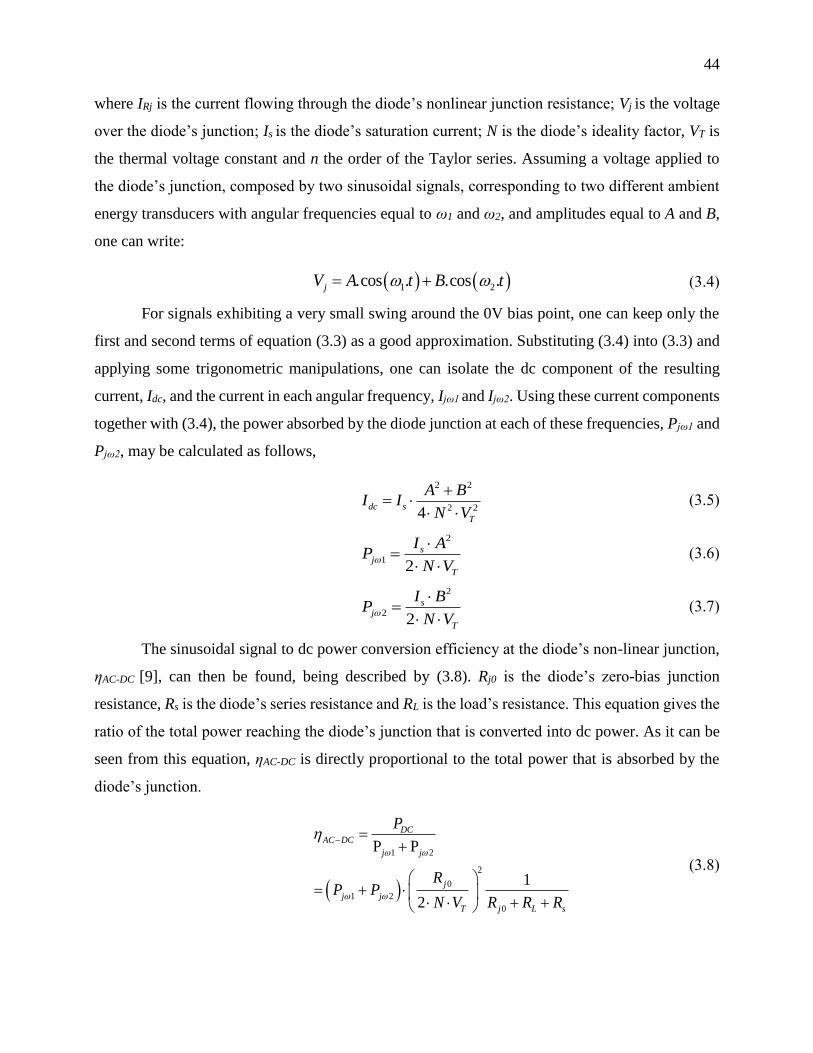
44
where IRj is the current flowing through the diode’s nonlinear junction resistance; Vj is the voltage
over the diode’s junction; Is is the diode’s saturation current; N is the diode’s ideality factor, VT is
the thermal voltage constant and n the order of the Taylor series. Assuming a voltage applied to
the diode’s junction, composed by two sinusoidal signals, corresponding to two different ambient
energy transducers with angular frequencies equal to ω1 and ω2, and amplitudes equal to A and B,
one can write:
1 2.cos . .cos .jV A t B t (3.4)
For signals exhibiting a very small swing around the 0V bias point, one can keep only the
first and second terms of equation (3.3) as a good approximation. Substituting (3.4) into (3.3) and
applying some trigonometric manipulations, one can isolate the dc component of the resulting
current, Idc, and the current in each angular frequency, Ijω1 and Ijω2. Using these current components
together with (3.4), the power absorbed by the diode junction at each of these frequencies, Pjω1 and
Pjω2, may be calculated as follows,
2 2
2 24dc s
T
A BI I
N V
(3.5)
2
12
sj
T
I AP
N V
(3.6)
2
22
sj
T
I BP
N V
(3.7)
The sinusoidal signal to dc power conversion efficiency at the diode’s non-linear junction,
ηAC-DC [9], can then be found, being described by (3.8). Rj0 is the diode’s zero-bias junction
resistance, Rs is the diode’s series resistance and RL is the load’s resistance. This equation gives the
ratio of the total power reaching the diode’s junction that is converted into dc power. As it can be
seen from this equation, ηAC-DC is directly proportional to the total power that is absorbed by the
diode’s junction.
1 2
2
0
1 2
0
P P
1
2
DCAC DC
j j
j
j j
T j L s
P
RP P
N V R R R
(3.8)
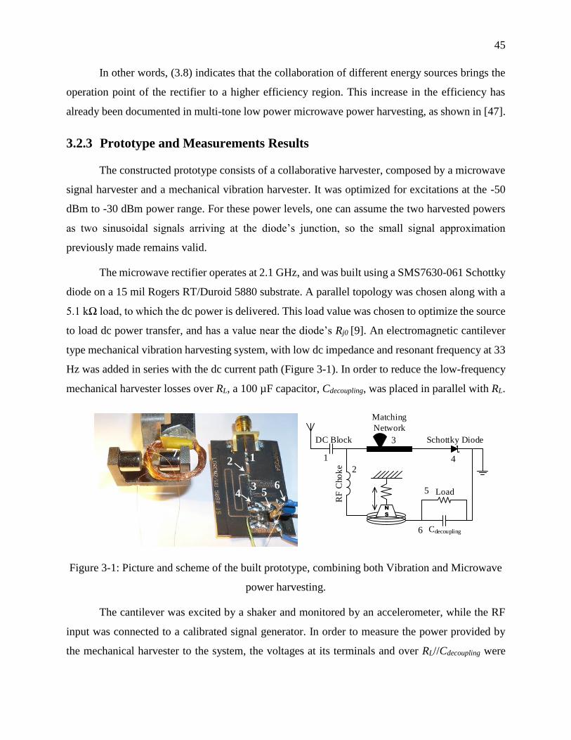
45
In other words, (3.8) indicates that the collaboration of different energy sources brings the
operation point of the rectifier to a higher efficiency region. This increase in the efficiency has
already been documented in multi-tone low power microwave power harvesting, as shown in [47].
3.2.3 Prototype and Measurements Results
The constructed prototype consists of a collaborative harvester, composed by a microwave
signal harvester and a mechanical vibration harvester. It was optimized for excitations at the -50
dBm to -30 dBm power range. For these power levels, one can assume the two harvested powers
as two sinusoidal signals arriving at the diode’s junction, so the small signal approximation
previously made remains valid.
The microwave rectifier operates at 2.1 GHz, and was built using a SMS7630-061 Schottky
diode on a 15 mil Rogers RT/Duroid 5880 substrate. A parallel topology was chosen along with a
5.1 kΩ load, to which the dc power is delivered. This load value was chosen to optimize the source
to load dc power transfer, and has a value near the diode’s Rj0 [9]. An electromagnetic cantilever
type mechanical vibration harvesting system, with low dc impedance and resonant frequency at 33
Hz was added in series with the dc current path (Figure 3-1). In order to reduce the low-frequency
mechanical harvester losses over RL, a 100 µF capacitor, Cdecoupling, was placed in parallel with RL.
The cantilever was excited by a shaker and monitored by an accelerometer, while the RF
input was connected to a calibrated signal generator. In order to measure the power provided by
the mechanical harvester to the system, the voltages at its terminals and over RL//Cdecoupling were
7
Figure 3-1: Picture and scheme of the built prototype, combining both Vibration and Microwave
power harvesting.
7 1
3 5
6 4
2 1
2
3
4
5
6
Matching
Network
Load
Cdecoupling
Schottky Diode
RF
Cho
ke
DC Block
N
S
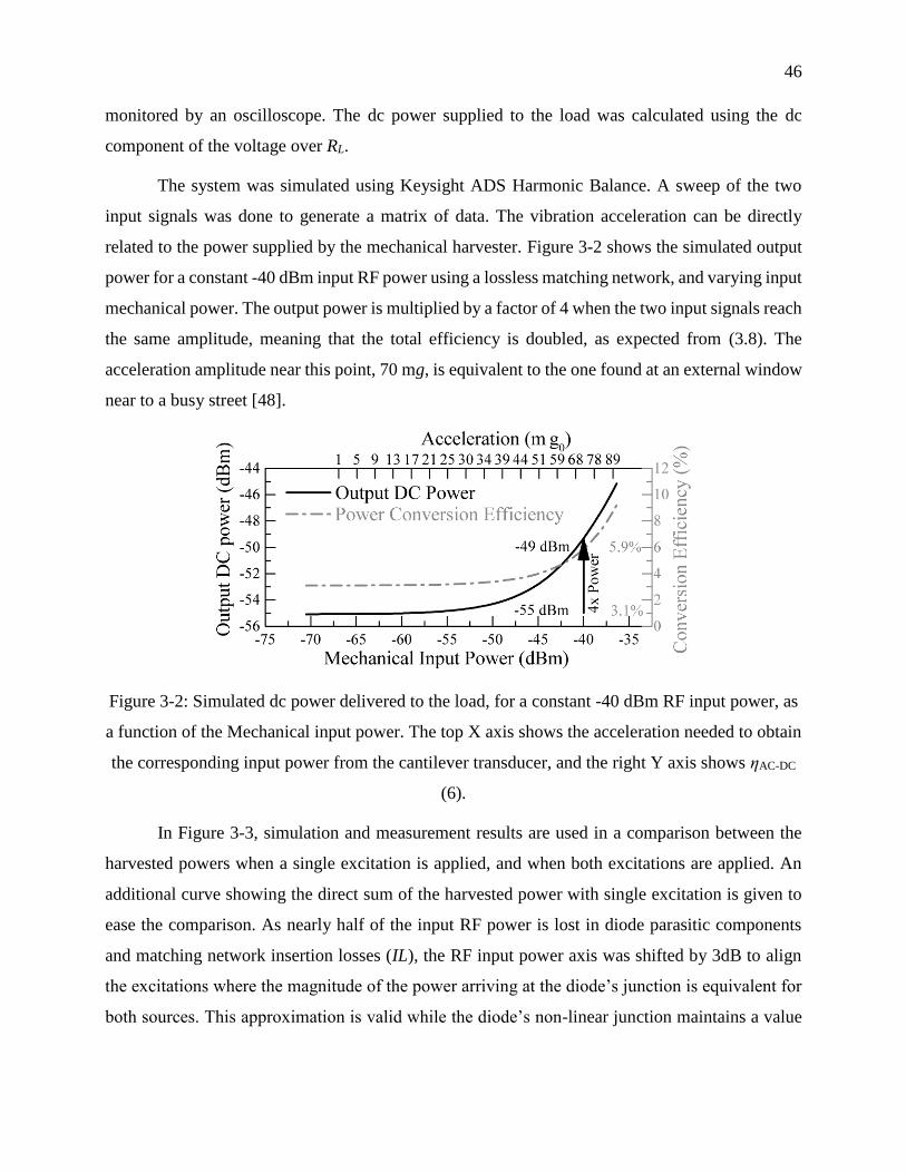
46
monitored by an oscilloscope. The dc power supplied to the load was calculated using the dc
component of the voltage over RL.
The system was simulated using Keysight ADS Harmonic Balance. A sweep of the two
input signals was done to generate a matrix of data. The vibration acceleration can be directly
related to the power supplied by the mechanical harvester. Figure 3-2 shows the simulated output
power for a constant -40 dBm input RF power using a lossless matching network, and varying input
mechanical power. The output power is multiplied by a factor of 4 when the two input signals reach
the same amplitude, meaning that the total efficiency is doubled, as expected from (3.8). The
acceleration amplitude near this point, 70 mg, is equivalent to the one found at an external window
near to a busy street [48].
Figure 3-2: Simulated dc power delivered to the load, for a constant -40 dBm RF input power, as
a function of the Mechanical input power. The top X axis shows the acceleration needed to obtain
the corresponding input power from the cantilever transducer, and the right Y axis shows ηAC-DC
(6).
In Figure 3-3, simulation and measurement results are used in a comparison between the
harvested powers when a single excitation is applied, and when both excitations are applied. An
additional curve showing the direct sum of the harvested power with single excitation is given to
ease the comparison. As nearly half of the input RF power is lost in diode parasitic components
and matching network insertion losses (IL), the RF input power axis was shifted by 3dB to align
the excitations where the magnitude of the power arriving at the diode’s junction is equivalent for
both sources. This approximation is valid while the diode’s non-linear junction maintains a value
47
near Rj0, for higher powers the decrease in Rj0 will result in a lower IL and diode parasitic losses
[9], and matching network retuning may be necessary.
Figure 3-3: Comparison between the harvesters working only with mechanical excitation, only
RF excitation or in hybrid mode, with both excitations applied at the same time. Scattered
symbols (measurements) and lines (simulation) were added for comparison, the light grey
symbols show the equivalent measurements power conversion efficiency. The percentage of the
input power converted into intermodulation products is also shown as a dashed line.
A 6 dB increase in the total power harvested by the hybrid strategy was obtained, when
compared to the single source harvesting. This gain is verified up to nearly -35 dBm input RF
power. Above this threshold, the excitation cannot be considered as being small-signal anymore,
and intermodulation products at the combination of the two excitation frequencies start to be
generated by the non-linear diode junction. This power is then lost on parasitic effects or re-radiated
by the antenna. The percentage of the total input power that is converted into intermodulation
products, as a function of the input power, is shown in Figure 3-3.
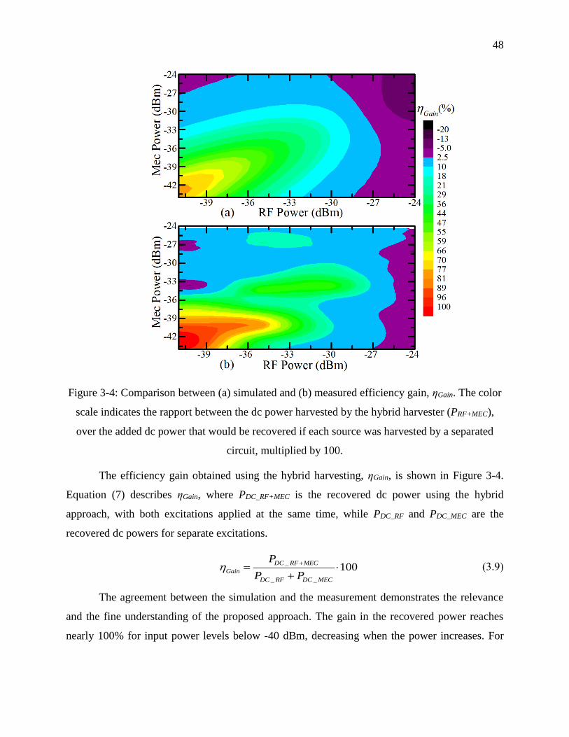
48
Figure 3-4: Comparison between (a) simulated and (b) measured efficiency gain, ηGain. The color
scale indicates the rapport between the dc power harvested by the hybrid harvester (PRF+MEC),
over the added dc power that would be recovered if each source was harvested by a separated
circuit, multiplied by 100.
The efficiency gain obtained using the hybrid harvesting, ηGain, is shown in Figure 3-4.
Equation (7) describes ηGain, where PDC_RF+MEC is the recovered dc power using the hybrid
approach, with both excitations applied at the same time, while PDC_RF and PDC_MEC are the
recovered dc powers for separate excitations.
_
_ _
100DC RF MEC
Gain
DC RF DC MEC
P
P P
(3.9)
The agreement between the simulation and the measurement demonstrates the relevance
and the fine understanding of the proposed approach. The gain in the recovered power reaches
nearly 100% for input power levels below -40 dBm, decreasing when the power increases. For

49
stronger input power levels, near -24 dBm, losses start to appear due to intermodulation products
generation.
3.2.4 Conclusion
This work has successfully demonstrated the increase in power harvesting efficiency at
power levels below -30 dBm, usually found in ambient power harvesting applications, by the use
of Collaborative Hybrid Power Harvesters.
The Power Harvester proposed by this work uses two different power sources to excite a
single rectification circuit, increasing the overall harvesting efficiency at low power levels. An
example was presented, of a collaborative hybrid power harvester of mechanical vibration and
microwave radiation, where output power gains up to nearly 100% were observed for -40 dBm and
lower input powers, in accordance to the small signal theory presented in the beginning of this
letter. Even though the proposed prototype uses these two power sources, the authors propose that
other alternate signal harvesters could be combined to obtain a similar result.
The proposed hybrid technique presents another advantage over the separated power
harvesting schemes, as the delivered dc power is already combined at the rectifying element. No
extra circuitry is needed to combine both dc outputs. Hence diminishing eventual power losses that
would occur during this process, simplifying the circuit and reducing its cost.
3.2.5 ACKNOWLEDGMENT
The authors would like to thank B. Besner and I. Nowlan, for allowing the use of the
acoustics laboratory installations, and also the Technicians in Poly-GRAMES research center.
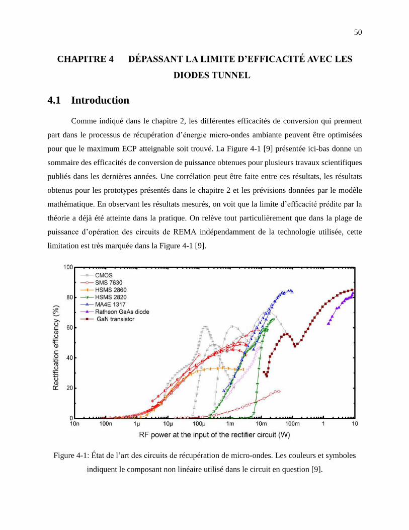
50
CHAPITRE 4 DÉPASSANT LA LIMITE D’EFFICACITÉ AVEC LES
DIODES TUNNEL
4.1 Introduction
Comme indiqué dans le chapitre 2, les différentes efficacités de conversion qui prennent
part dans le processus de récupération d’énergie micro-ondes ambiante peuvent être optimisées
pour que le maximum ECP atteignable soit trouvé. La Figure 4-1 [9] présentée ici-bas donne un
sommaire des efficacités de conversion de puissance obtenues pour plusieurs travaux scientifiques
publiés dans les dernières années. Une corrélation peut être faite entre ces résultats, les résultats
obtenus pour les prototypes présentés dans le chapitre 2 et les prévisions données par le modèle
mathématique. En observant les résultats mesurés, on voit que la limite d’efficacité prédite par la
théorie a déjà été atteinte dans la pratique. On relève tout particulièrement que dans la plage de
puissance d’opération des circuits de REMA indépendamment de la technologie utilisée, cette
limitation est très marquée dans la Figure 4-1 [9].
Figure 4-1: État de l’art des circuits de récupération de micro-ondes. Les couleurs et symboles
indiquent le composant non linéaire utilisé dans le circuit en question [9].
51
Dans la Figure 4-1, les ECP semblent arriver à une limite maximale dans la plage de
puissances en dessous de 3 µW (approximativement -25 dBm), indépendamment de la technologie
utilisée pour le redressement (diode Schottky, CMOS, …). Comme il va en être discuté dans
l’article présenté dans ce chapitre, l’origine de ce seuil d’efficacité provient du mécanisme
physique qui régit le transport des électrons dans les jonctions des diodes Schottky et dans les
transistors utilisés dans les composantes CMOS – les émissions thermo-ioniques.
Selon l’équation (2-11), répétée ici-bas, l’efficacité de conversion de puissance RF-cc est
proportionnelle au carré de la responsivité en courant du dispositif non linéaire utilisé pour le
redressement de la puissance. Dans ce chapitre, l’utilisation de diodes tunnel pour atteindre une
ECP plus élevée que celle obtenue avec les diodes Schottky est étudiée. Le transport des électrons
dans ces diodes, différemment des diodes Schottky, n’est pas régi par l’effet thermo-ionique. Cela
permet le développement de diodes ayant une responsivité plus élevée que celle atteignable avec
les diodes Schottky, permettant ainsi que des ECP plus élevées que les atteintes jusqu’à ici soient
ainsi obtenues.
0 0
22
0
0
( ). . .
( ) I
j loadDCRFDC I jf
jf L s j load
R IPP
P R R R I
(3.10)
52
4.2 Article 3 — Breaking the Efficiency Barrier for Ambient Microwave
Power Harvesting With Heterojunction Backward Tunnel Diodes
Carlos H. P. Lorenz, Student Member IEEE, Simon Hemour, Member IEEE, Wenjun Li, Yi Xie,
Jules Gauthier, Member, IEEE, Patrick Fay, Senior Member IEEE, Ke Wu, Fellow, IEEE
Soumis le 1er juillet 2015 à « IEEE Transactions on Microwave Theory and Techniques »,
accepté le 13 octobre 2015.
Abstract — Harvesting low-density ambient microwave power as an alternative power source
for small ubiquitous wireless nodes has been proposed in recent papers discussing emerging
technologies like the Internet of Things and Smart Cities. However a literature review of the
state-of-the-art Schottky diode based microwave rectifiers shows that a maximum efficiency
has been reached for such devices operating in the low-power regime, as is the case for
ambient microwave power-harvesters. This work examines the underlying physical
mechanisms responsible for this RF-to-dc power conversion efficiency limitation, and
explores a high I-V curvature backward tunnel diode to overcome this efficiency limitation.
Measurements of the 2.4 GHz RF-to-dc power conversion efficiency at -40 dBm input power
demonstrates that the backward tunnel diode outperforms the HSMS-285B Schottky diode
by a factor of 10.5 and the Skyworks SMS7630 by a factor of 5.5 in a lossless matching
network scenario. A prototype built using a new GSG probe embedded with a matching
circuit showed a total power conversion efficiency of 3.8% for -40 dBm input power and
18.2% for -30 dBm input power at 2.35 GHz.
Index Terms— Backward tunnel diode, Schottky diode, microwave power harvesting,
microwave power rectification, rectenna.

53
2
4.2.1 Introduction
The way the internet is perceived by its users is going through a significant transformation.
Today, nearly two billion people have access to the internet [2], using it to browse websites, play
games, work, send and receive e-mails and messages, among many other on-line applications. Most
of these applications, however, share a common characteristic: an end-user terminal. Nonetheless
an important revolution is in progress, in which ubiquitous objects will be more and more
connected to the internet or other local networks, leading to the Internet of Things (IoT) [1, 2].
Some emerging applications of this new paradigm in networking include monitoring the structural
health of buildings and monuments, smart roads to help detect heavy traffic so that efficient
itineraries can be suggested and traffic light timings can be optimized, remote health monitoring
of patients, to cite just a few [16].
Emerging hardware technologies are being studied to enable these Smart Cities, Smart
Building Automation and Monitoring, as well as Wearable Devices applications. These usually
require wireless connections and small form-factor energy sources to remotely power the
ubiquitous sensing and controlling devices, without the burden of a heavy and bulky battery that
may be difficult to replace – as in the case of body implants and sensors embedded into building
Manuscript received July 1, 2015; revised September 30, 2015; accepted October 13, 2015. Date of publication
November 18, 2015; date of current version December 02, 2015. This work was supported in part by the Natural
Sciences and Engineering Research Council of Canada (NSERC) and CREATE PERSWADE Training Program. This
paper is an expanded version from the IEEE MTT-S International Microwave Symposium, Phoenix, AZ, USA, May
17-22, 2015.
C. H. P. Lorenz, S. Hemour, J. Gauthier and K. Wu are with the Poly-Grames Research Center, École Polytechnique
de Montréal, Montreal, QC H3T 1J4, Canada. (e-mail: [email protected]).
W. Li, Y. Xie and P. Fay are with the Department of Electrical Engineering, University of Notre Dame, Notre Dame,
IN 46556, USA. (e-mail: [email protected]).
Color versions of one or more of the figures in this paper are available online at http://ieeexplore.ieee.org.
Digital Object Identifier: 10.1109/TMTT.2015.2495356

54
structural parts. Resonant power transfer technology has shown to be a good alternative when a
charger may be placed in close proximity to the wireless device of interest, as is the case for parked
electric vehicles and even body implants that may be charged at periodic intervals [49]. However,
very short operational distances between the charger and device becomes a fundamental obstacle
when omnipresent, distributed sensor networks are deployed. Microwave Power Harvesting
(MPH) has been proposed as an alternative wireless power source for such low power consumption
and low duty cycle ubiquitous devices [8, 50, 51].
However, an overview of the state of the art in the field of microwave power harvesting
suggests that a limitation in the efficiency of Schottky diode-based converters at low incident power
levels has been reached [8, 9, 13]. In practice, microwave power rectifiers capable of operating
below -30 dBm are needed for ambient microwave power harvesting (AMPH) as indicated in recent
ambient microwave power density assessments [3, 8]. However, to date RF-to-dc conversion
efficiency has not yet reached even 10% at frequencies above 1 GHz at such low-density power
levels. Overcoming this performance barrier is essential for AMPH systems to become a practical
reality.
Schottky diodes rely on the thermionic effect, which limits the zero-bias current
responsivity ℜI0 to 19.34 A/W at 300K [13]. As shown in [9, 13], the rectification efficiency of
microwave rectifiers operating in the diode’s square-law region is directly proportional to the
square of ℜI0. Backward tunnel diodes, which make use of quantum mechanical tunneling rather
than thermionic emission, have been reported that overcome the Schottky diodes’ inherent ℜI0,
reaching values near 24 A/W for devices optimized for millimeter-wave operation [13, 38] or even
as high as 35 A/W for lower-frequency devices [52]. This paper presents a deeper evaluation of the
application of such diodes to overcome the low-power RF-to-dc conversion efficiency limitation
observed with Schottky diode microwave rectifiers, an idea which was first introduced in [10] and
is extended in this paper. A comparison between a backward diode and an HSMS-285B Schottky
diode is presented, demonstrating an increase in the RF-to-dc conversion efficiency at extremely
low incident power levels, as required when harvesting ambient power below -30 dBm.
4.2.2 Microwave Power Harvesting
In order to explore possible ways of increasing the power conversion efficiency PCE (3.11)
of ambient microwave power harvesters, it is, first of all, necessary to understand the mechanisms

55
that play a role in the energy rectification process at very low input powers levels, as found in
ambient microwave power harvesting scenarios. In such applications, the expected operation power
range has peaks in the vicinity of -30 dBm and below, with a typical average power of -40 dBm
and below [3, 8]. At such power levels the square-law microwave power rectification model
presented in [9] can be used as a good approximation.
In this rectification model, the power conversion mechanism is sub-divided into different
steps, each one with an intrinsic efficiency. These efficiencies combine to produce the total
rectifier’s PCE, as summarized below:
ηm is the matching network efficiency;
ηp is the parasitic efficiency;
η0 is the non-linear junction RF-to-dc power conversion efficiency;
ηdcT is the dc power transfer efficiency, which gives the percentage of the total rectified dc
power that is actually delivered to the load.
The total power conversion efficiency PCE can thus be calculated using (3.11):
0LOAD
m p dcT
RF
PPCE
P (3.11)
where PLOAD is the dc power delivered to the load and PRF is the input RF power. The non-linear
device characteristics influence in different ways each of these efficiencies. In the case of diodes,
which are the subject of the study presented in this work, the Shockley diode model with package
parasitic components is used, as shown in Figure 4-2. In this figure Rj represents the diode’s non-
linear junction resistance, Cj the junction capacitance, Cp the package parasitic capacitance, Lp, the
package inductance and RS the series resistance.
Figure 4-2: Shockley diode model with package/pads parasitic components.

56
Using this model, the total η0∙ηdcT efficiency when the load connected to the diode is equal
to Rj0 is given by [9]:
2
0 0
04
I j
dcT j
RP
(3.12)
where Pj is the microwave power delivered to the junction resistance, Rj0 is the junction resistance
at zero-bias, and ℜI0 is the diode zero-bias current responsivity. The parasitic efficiency can then
be calculated by using [9]:
2
2
0 0 0
1
1p
j s jC R R
(3.13)
where ω0 is the angular frequency of operation.
The matching network efficiency ηm largely depends on the matching topology and
circuit/component technology used to implement the matching network. However, (3.14) and
(3.15) [21] can be used to estimate the relative increase or decrease of ηm achieved with different
candidate diodes, provided that the quality factor of the matching network Qm can be maintained
at the same level. Such an assumption of constant Qm is true if the source and load mismatch does
not change substantially (i.e., the diode impedances under consideration are not dramatically
different). Under these assumptions,
1
1m
r
m
Q
Q
(3.14)
1HIGHr
LOW
RQ
R (3.15)
where Qr is the required quality factor, which depends on the mismatch between the highest and
lowest impedances (RHIGH and RLOW, respectively) that are to be matched. In the case of diode-
based matching for AMPH, this is typically the source impedance and the diode’s Rj0.
Using equations (3.11) through (3.15) one can understand the diode parameters that need
to be optimized in order to maximize the power conversion efficiency.
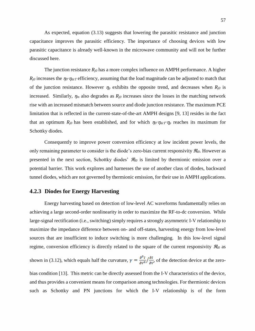
57
As expected, equation (3.13) suggests that lowering the parasitic resistance and junction
capacitance improves the parasitic efficiency. The importance of choosing devices with low
parasitic capacitance is already well-known in the microwave community and will not be further
discussed here.
The junction resistance Rj0 has a more complex influence on AMPH performance. A higher
Rj0 increases the η0∙ηdcT efficiency, assuming that the load magnitude can be adjusted to match that
of the junction resistance. However ηp exhibits the opposite trend, and decreases when Rj0 is
increased. Similarly, ηm also degrades as Rj0 increases since the losses in the matching network
rise with an increased mismatch between source and diode junction resistance. The maximum PCE
limitation that is reflected in the current-state-of-the-art AMPH designs [9, 13] resides in the fact
that an optimum Rj0 has been established, and for which η0∙ηdcT∙ηp reaches its maximum for
Schottky diodes.
Consequently to improve power conversion efficiency at low incident power levels, the
only remaining parameter to consider is the diode’s zero-bias current responsivity ℜI0. However as
presented in the next section, Schottky diodes’ ℜI0 is limited by thermionic emission over a
potential barrier. This work explores and harnesses the use of another class of diodes, backward
tunnel diodes, which are not governed by thermionic emission, for their use in AMPH applications.
4.2.3 Diodes for Energy Harvesting
Energy harvesting based on detection of low-level AC waveforms fundamentally relies on
achieving a large second-order nonlinearity in order to maximize the RF-to-dc conversion. While
large-signal rectification (i.e., switching) simply requires a strongly asymmetric I-V relationship to
maximize the impedance difference between on- and off-states, harvesting energy from low-level
sources that are insufficient to induce switching is more challenging. In this low-level signal
regime, conversion efficiency is directly related to the square of the current responsivity ℜI0 as
shown in (3.12), which equals half the curvature, , of the detection device at the zero-
bias condition [13]. This metric can be directly assessed from the I-V characteristics of the device,
and thus provides a convenient means for comparison among technologies. For thermionic devices
such as Schottky and PN junctions for which the I-V relationship is of the form

58
, one can see that at room temperature,
independent of technology or the details of device design. This imposes fundamental physical
limits on the ultimately achievable performance of thermionic detectors for energy harvesting
applications. To circumvent this limitation, devices based on alternative physical operation
principles for which is not limited to q/kT are potentially attractive. One promising physical
mechanism that can be leveraged to obtain a higher curvature is interband tunneling. In contrast to
Schottky diodes, PN junctions, and transistor-based passive detectors (e.g. diode-connected FETs,
Schottky diodes using HEMT gates) in which carriers in a single band interact with a voltage-
controlled potential barrier as the basis for detection and rectification, interband tunnel diodes are
governed by the combination of the density of states and occupancy probabilities on both sides of
the tunnel junction as well as the tunneling probability. In this way the density of states in both the
conduction and valence bands, as well as the details of the tunnel barrier, can be used to engineer
devices with increased second-order nonlinearity and thus offer the potential for improved
detection and conversion efficiency. An analytical treatment of homojunction interband tunnel
diodes can be found in [53]; within the simplified model used, an arbitrarily large curvature can be
achieved by a proper selection of the Fermi levels within the device [53]. Fundamentally these
devices can offer larger curvatures than thermionic-emission based devices because the overlap
between the occupied electron and hole densities of states is “filtered” by the bandgaps at the
heterojunction, leading to a truncation of the Fermi-Dirac distribution for the carriers. Devices of
this type have been demonstrated experimentally as millimeter-wave detectors [54], and curvatures
as high as 70 V-1 have been reported experimentally [52], broadly consistent with the expectations
with theory. It should be noted that in order to achieve these high curvatures, a “backward” tunnel
diode structure is needed, in contrast to an Esaki diode [55, 56]. In the case of an Esaki diode,
extremely high doping is used on both sides of the junction, leading to low junction resistance and
the onset of negative differential resistance in the forward characteristic. For detector and harvester
applications, however, the negative differential resistance is not desirable (the curvature changes
sign at the onset of negative differential resistance, leading to a partial cancellation of the detected
signal with an increasing input power) and the second-order curvature near zero bias is smaller
than with the more modestly-doped backward diode structures [53].

59
However, homojunction tunnel diodes such as those described above also pose some
challenges in energy harvesting applications. Of particular concern for RF and microwave
applications, homojunction tunnel diodes have a large capacitance per unit area (as a direct
consequence of the use of heavy doping to achieve the thin depletion region and band degeneracy
required to enable tunneling). This limits the frequency range of application, due to increased
parasitic losses, as well as the bandwidth achievable with reactive matching networks. It has also
been reported that Ge-based tunnel junctions can pose reliability and manufacturability challenges
[57].
As an alternative, heterostructure backward tunnel diodes are an attractive approach. These
devices maintain the fundamental operational principles of homojunction tunnel diodes (interband
tunneling) and thus the possibility for high curvature, while at the same time introducing significant
additional degrees of freedom in the device design to allow optimization of the device performance
for specific applications. For example, devices of this type have previously been demonstrated to
provide high-sensitivity, low-noise microwave and millimeter-wave detection [38, 58-60] for
applications such as passive millimeter-wave imaging, with an extremely low noise equivalent
power (NEP) of 0.18 pW/Hz1/2 [38]. This record-low NEP is made possible by a combination of
both extremely low device noise, in conjunction with higher curvature arising from the operational
physics. To maximize performance for detection, the devices are designed to maximize the second
order nonlinearity at zero bias, thereby allowing the detectors to be used without externally applied
bias. This dramatically reduces 1/f noise (resulting in nearly thermal-noise-limited performance)
[59, 61], and it has been shown that zero-bias second-order nonlinearity in excess of what is
possible with Schottky diodes can be achieved [38]. This degree of control of the device
characteristics is made possible by the substantial design flexibility in heterostructure devices.
Low-level RF energy harvesters have similar requirements, i.e., strong nonlinearity near zero bias
is needed for efficient RF-to-dc conversion, and thus these devices are also attractive for this
application.
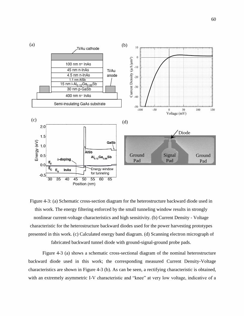
60
Figure 4-3 (a) shows a schematic cross-sectional diagram of the nominal heterostructure
backward diode used in this work; the corresponding measured Current Density-Voltage
characteristics are shown in Figure 4-3 (b). As can be seen, a rectifying characteristic is obtained,
with an extremely asymmetric I-V characteristic and “knee” at very low voltage, indicative of a
(a)
(c) (d)
Figure 4-3: (a) Schematic cross-section diagram for the heterostructure backward diode used in
this work. The energy filtering enforced by the small tunneling window results in strongly
nonlinear current-voltage characteristics and high sensitivity. (b) Current Density - Voltage
characteristic for the heterostructure backward diodes used for the power harvesting prototypes
presented in this work. (c) Calculated energy band diagram. (d) Scanning electron micrograph of
fabricated backward tunnel diode with ground-signal-ground probe pads.
Diode
Ground
Pad Ground
Pad
Signal
Pad
(b)

61
strong curvature. In addition, the turn-on is in the ‘reverse’ direction (i.e., in the opposite sense
from a conventional PN junction diode), as expected for a backward diode. As discussed
previously, the efficiency of a power harvester is directly related to the junction resistance and
curvature. Due to the interband tunneling mechanism in heterostructure backward diodes, can be
much larger than what is possible with conventional Schottky or other thermionic emission-based
devices; optimizing a heterostructure backward tunnel diode for energy harvesting applications
requires maximizing the curvature while keeping the junction resistance at an acceptably low level.
The key parameters that enable control over the device performance are the anode and cathode
doping concentrations (and doping profiles), the tunnel barrier thickness, and the energy band
offset between the valence band in the anode and the conduction band in the cathode. As one
example, Figure 4-3 (c) shows the computed energy band diagram for the backward diode structure
shown in Figure 4-3 (a). The choice of an aluminum composition of 12% in the anode layer leads
to a small overlap between the conduction and valence bands, and thus as shown Figure 4-3 (c),
only carriers occupying a narrow range of energies can participate in tunneling through the AlSb
tunnel barrier. Carriers with higher energies in either the anode or cathode are blocked by the
bandgaps (i.e., are filtered) and cannot contribute to the current [53, 62]. The choice of the AlSb
tunnel barrier thickness allows an independent control of the junction resistance (since to first order
tunneling probability is exponential in barrier thickness) without altering the densities of states in
the cathode and anode appreciably. The doping profiles in the anode and cathode are selected to
enhance transmission through the structure, with a -doping plane incorporated into the cathode in
this structure to provide a nearly flat band profile.
The device heterostructure was grown by molecular beam epitaxy on a semi-insulating
GaAs substrate. Device fabrication included evaporated Ti/Au anode and cathode contacts, mesa
isolation using selective wet chemical etchants [63], and passivation with benzocyclobutene. The
devices had an area of approximately 0.5 µm2; electron beam lithography was used to accurately
define the device active area. Optical lithography was used to define the pads, mesas, contacts and
passivation layers.
For the power harvesting experiments performed here, devices with the nominal
heterostructure shown in Figure 4-3 (a) were used; this results in a measured zero-bias curvature
=45 V-1, and as will be shown, this improved curvature and low turn-on voltage result in high

62
power harvester efficiency even at low incident RF levels. To further increase the harvester
efficiency, increased curvature is desirable. Fundamentally, increases in curvature are correlated
with improved energy filtering at the tunnel junction; one promising approach for narrowing the
energy window over which tunneling can occur is by modifying the composition of the AlGaSb
anode (i.e., increasing the Al composition results in a smaller tunneling window). Physics-based
simulations of heterostructures with the same basic form as shown in Figure 4-3 (c), except with
varying AlxGa1-xSb compositions have been performed, and the junction resistance and curvature
expected from these models is shown in Figure 4-4. Details of the modeling framework have been
reported previously [64]. As can be seen in Figure 4-4, increasing the Al composition in the anode
results in a significant increase in curvature, with curvatures approaching 90 V-1 possible for
compositions of approximately 25%. This increased curvature arises from the more narrowly-
filtered carrier energy, but as expected this narrower energy range for tunneling is also
accompanied by an increase in junction resistance. Our models project a harvester efficiency η0∙ηdcT
of 63% for such a diode at -40 dBm input power, indicating that despite the promising results
obtained to date and reported here, considerable additional improvements are possible. While
further increases in curvature can be obtained, they come at the expense of a significant increase
in junction resistance that may limit overall conversion efficiency. The junction resistance increase
can be counterbalanced to some extent by increasing the diode’s junction area, however at the cost
of an increased junction capacitance. As a result, the optimum anode composition and junction area
is also a function of the intended frequency of operation. Detailed study of these tradeoffs is the
subject of ongoing work.
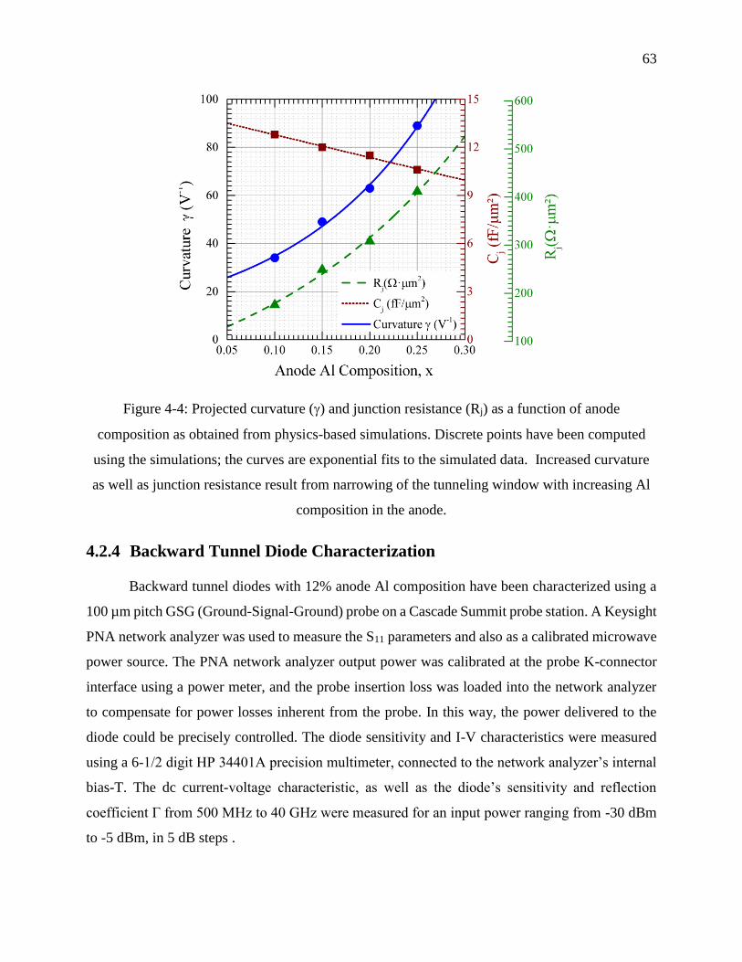
63
Figure 4-4: Projected curvature () and junction resistance (Rj) as a function of anode
composition as obtained from physics-based simulations. Discrete points have been computed
using the simulations; the curves are exponential fits to the simulated data. Increased curvature
as well as junction resistance result from narrowing of the tunneling window with increasing Al
composition in the anode.
4.2.4 Backward Tunnel Diode Characterization
Backward tunnel diodes with 12% anode Al composition have been characterized using a
100 µm pitch GSG (Ground-Signal-Ground) probe on a Cascade Summit probe station. A Keysight
PNA network analyzer was used to measure the S11 parameters and also as a calibrated microwave
power source. The PNA network analyzer output power was calibrated at the probe K-connector
interface using a power meter, and the probe insertion loss was loaded into the network analyzer
to compensate for power losses inherent from the probe. In this way, the power delivered to the
diode could be precisely controlled. The diode sensitivity and I-V characteristics were measured
using a 6-1/2 digit HP 34401A precision multimeter, connected to the network analyzer’s internal
bias-T. The dc current-voltage characteristic, as well as the diode’s sensitivity and reflection
coefficient Γ from 500 MHz to 40 GHz were measured for an input power ranging from -30 dBm
to -5 dBm, in 5 dB steps .
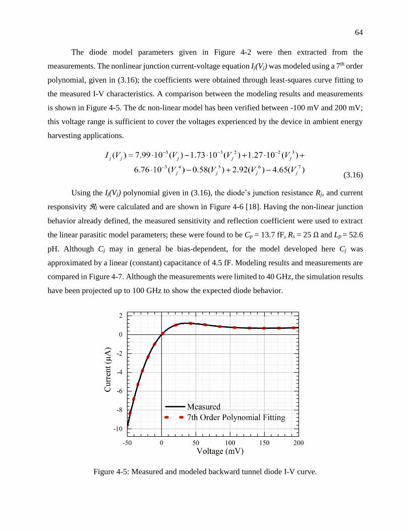
64
The diode model parameters given in Figure 4-2 were then extracted from the
measurements. The nonlinear junction current-voltage equation Ij(Vj) was modeled using a 7th order
polynomial, given in (3.16); the coefficients were obtained through least-squares curve fitting to
the measured I-V characteristics. A comparison between the modeling results and measurements
is shown in Figure 4-5. The dc non-linear model has been verified between -100 mV and 200 mV;
this voltage range is sufficient to cover the voltages experienced by the device in ambient energy
harvesting applications.
(3.16)
Using the Ij(Vj) polynomial given in (3.16), the diode’s junction resistance Rj, and current
responsivity ℜI were calculated and are shown in Figure 4-6 [18]. Having the non-linear junction
behavior already defined, the measured sensitivity and reflection coefficient were used to extract
the linear parasitic model parameters; these were found to be Cp = 13.7 fF, Rs = 25 Ω and Lp = 52.6
pH. Although Cj may in general be bias-dependent, for the model developed here Cj was
approximated by a linear (constant) capacitance of 4.5 fF. Modeling results and measurements are
compared in Figure 4-7. Although the measurements were limited to 40 GHz, the simulation results
have been projected up to 100 GHz to show the expected diode behavior.
Figure 4-5: Measured and modeled backward tunnel diode I-V curve.

65
The modeled diode resistance and responsivity near zero-bias are shown in Figure 4-6, over
the expected operating region for the AMPH application presented here. From this figure, a ℜI0 of
21.65 A/W and Rj0 of 12.5 kΩ are obtained for the particular backward tunnel diode used for this
work.
Figure 4-6: Calculated backward diode Rj and ℜI, using the 7th order polynomial fitted to the
measured I-V relationship.
Assuming that the parasitic efficiency is comparable for Schottky and tunnel diodes, the
increase in the diode’s ℜI0 from 19.34 A/W in the ideal Schottky diode case to the measured tunnel
diode responsivity of 21.65 A/W indicates that the efficiency at square-law power levels is
expected to increase by a factor of 1.25 according to (3.12).

66
Figure 4-7: Comparison between measured and modeled backward diode RF characteristics at -
30 dBm. (a) Input impedance, Zin, real and imaginary components. (b) Voltage sensitivity; the
simulation has been projected to 100GHz.
4.2.5 Comparison of Backward Tunnel Diode and Schottky Diode Microwave
Rectifiers
Neglecting the matching losses and considering that parasitic losses are negligible at 2.45
GHz due to very low Cj, the studied backward diode has a calculated RF-to-dc power conversion

67
efficiency equal to 14.7% at -40 dBm input power. Two commonly used Schottky diodes in AMPH
applications were also evaluated and compared to the proposed backward diode, these are the
Avago HSMS-2850 and the Skyworks SMS7630 diodes. Table 4-1 compares the expected power
conversion efficiencies at -40 dBm input power, 2.4 GHz center frequency, and resistive load
matched to each diode’s Rj0. The efficiencies were calculated using the backward diode model
parameters presented previously, and Schottky diodes parameters from the manufacturer
datasheets. This comparison highlights two important advantages that arise from the use of the
backward tunnel diode in AMPH applications. The first is the discussed increase in the η0∙ηdcT
efficiency product due to the increased ℜI0. However another advantage that should be noted is the
very high parasitic efficiency due to the low junction capacitance that results from the backward
tunnel diode structure used here.
Table 4-1: Rectifier Efficiencies at -40dBm @ 2.4 GHZ
Diode ℜI0
(A/W)
Rj0
kΩ
Cj0
fF
Efficiency (%)
𝞰0∙𝞰dcT 𝞰p PCE
Backward 21.65 12.5 4.5 14.7 99.7 14.6
Ideal Schottky 19.34 12.5 NA 11.7 NA NA
HSMS285B 18.25 9.13 180 7.6 13.9 1.1
SMS7630 18.42 5.43 140 4.6 45.4 2.1
From Table 4-1, it can be seen that a large advantage is expected when using backward
tunnel diode in AMPH applications; the expected PCE for the tunnel diode case is nearly 7 times
the PCE of the SMS7630 diode at microwave input power levels typical of ambient harvesting
applications.
In order to verify the increase in PCE predicted by the theory, both HSMS-285B and the
backward diode rectification efficiencies were measured. The choice of the Schottky diode was
based on the value of Rj0, which should be near to that presented by the backward diode to ensure
a valid comparison.
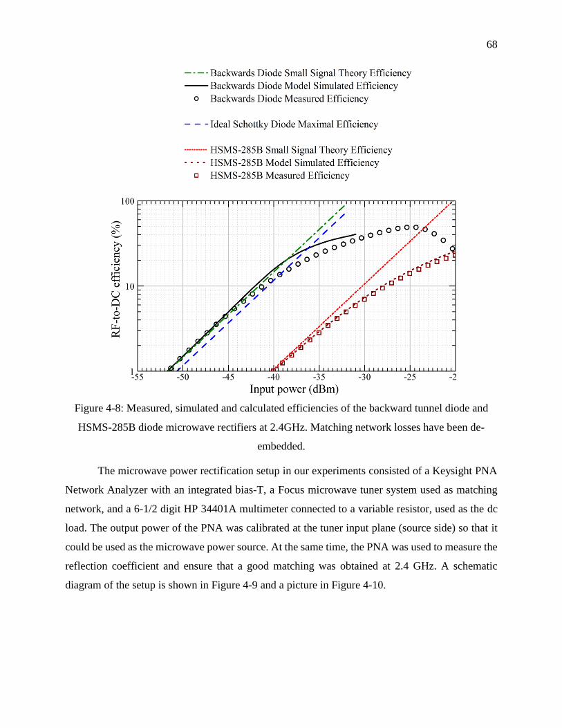
68
Figure 4-8: Measured, simulated and calculated efficiencies of the backward tunnel diode and
HSMS-285B diode microwave rectifiers at 2.4GHz. Matching network losses have been de-
embedded.
The microwave power rectification setup in our experiments consisted of a Keysight PNA
Network Analyzer with an integrated bias-T, a Focus microwave tuner system used as matching
network, and a 6-1/2 digit HP 34401A multimeter connected to a variable resistor, used as the dc
load. The output power of the PNA was calibrated at the tuner input plane (source side) so that it
could be used as the microwave power source. At the same time, the PNA was used to measure the
reflection coefficient and ensure that a good matching was obtained at 2.4 GHz. A schematic
diagram of the setup is shown in Figure 4-9 and a picture in Figure 4-10.
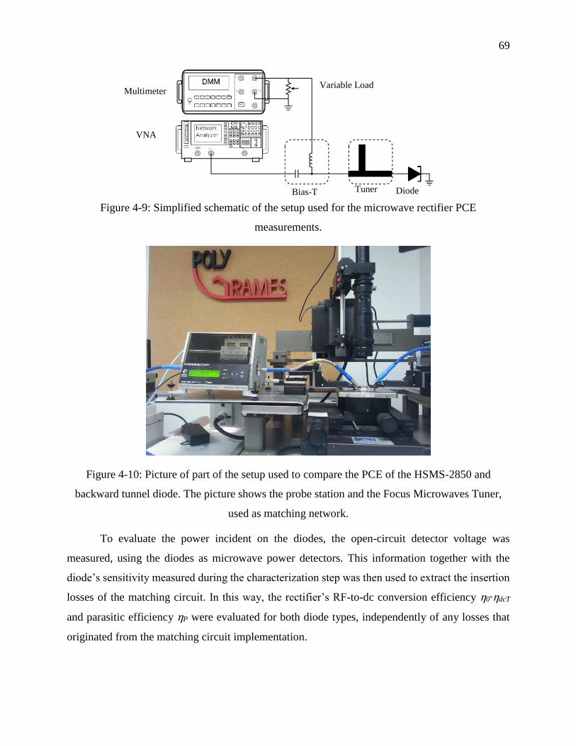
69
Figure 4-9: Simplified schematic of the setup used for the microwave rectifier PCE
measurements.
Figure 4-10: Picture of part of the setup used to compare the PCE of the HSMS-2850 and
backward tunnel diode. The picture shows the probe station and the Focus Microwaves Tuner,
used as matching network.
To evaluate the power incident on the diodes, the open-circuit detector voltage was
measured, using the diodes as microwave power detectors. This information together with the
diode’s sensitivity measured during the characterization step was then used to extract the insertion
losses of the matching circuit. In this way, the rectifier’s RF-to-dc conversion efficiency η0∙ηdcT
and parasitic efficiency ηP were evaluated for both diode types, independently of any losses that
originated from the matching circuit implementation.
Tuner Bias-T Diode
Variable Load
VNA
Multimeter
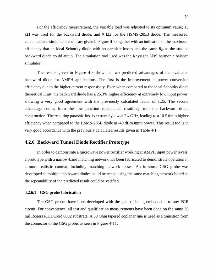
70
For the efficiency measurement, the variable load was adjusted to its optimum value; 13
kΩ was used for the backward diode, and 9 kΩ for the HSMS-285B diode. The measured,
calculated and simulated results are given in Figure 4-8 together with an indication of the maximum
efficiency that an ideal Schottky diode with no parasitic losses and the same Rj0 as the studied
backward diode could attain. The simulation tool used was the Keysight ADS harmonic balance
simulator.
The results given in Figure 4-8 show the two predicted advantages of the evaluated
backward diode for AMPH applications. The first is the improvement in power conversion
efficiency due to the higher current responsivity. Even when compared to the ideal Schottky diode
theoretical limit, the backward diode has a 25.3% higher efficiency at extremely low input power,
showing a very good agreement with the previously calculated factor of 1.25. The second
advantage comes from the low junction capacitance resulting from the backward diode
construction. The resulting parasitic loss is extremely low at 2.4 GHz, leading to a 10.5 times higher
efficiency when compared to the HSMS-285B diode at -40 dBm input power. This result too is in
very good accordance with the previously calculated results given in Table 4-1.
4.2.6 Backward Tunnel Diode Rectifier Prototype
In order to demonstrate a microwave power rectifier working at AMPH input power levels,
a prototype with a narrow-band matching network has been fabricated to demonstrate operation in
a more realistic context, including matching network losses. An in-house GSG probe was
developed so multiple backward diodes could be tested using the same matching network board so
the repeatability of the predicted result could be verified.
4.2.6.1 GSG probe fabrication
The GSG probes have been developed with the goal of being embeddable to any PCB
circuit. For convenience, all test and qualification measurements have been done on the same 30
mil Rogers RT/Duroid 6002 substrate. A 50 Ohm tapered coplanar line is used as a transition from
the connector to the GSG probe, as seen in Figure 4-11.
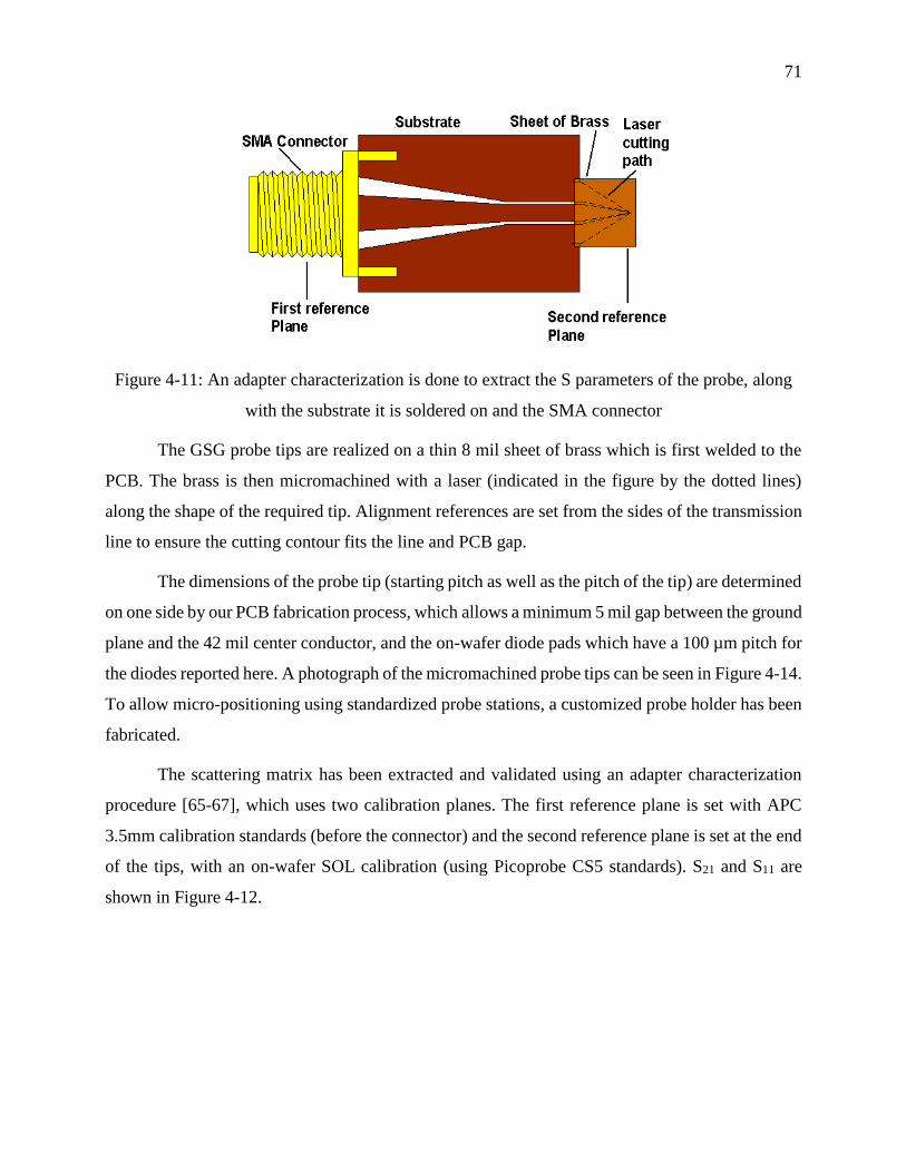
71
Figure 4-11: An adapter characterization is done to extract the S parameters of the probe, along
with the substrate it is soldered on and the SMA connector
The GSG probe tips are realized on a thin 8 mil sheet of brass which is first welded to the
PCB. The brass is then micromachined with a laser (indicated in the figure by the dotted lines)
along the shape of the required tip. Alignment references are set from the sides of the transmission
line to ensure the cutting contour fits the line and PCB gap.
The dimensions of the probe tip (starting pitch as well as the pitch of the tip) are determined
on one side by our PCB fabrication process, which allows a minimum 5 mil gap between the ground
plane and the 42 mil center conductor, and the on-wafer diode pads which have a 100 µm pitch for
the diodes reported here. A photograph of the micromachined probe tips can be seen in Figure 4-14.
To allow micro-positioning using standardized probe stations, a customized probe holder has been
fabricated.
The scattering matrix has been extracted and validated using an adapter characterization
procedure [65-67], which uses two calibration planes. The first reference plane is set with APC
3.5mm calibration standards (before the connector) and the second reference plane is set at the end
of the tips, with an on-wafer SOL calibration (using Picoprobe CS5 standards). S21 and S11 are
shown in Figure 4-12.

72
Figure 4-12: Reflection and transmission parameter of the probe extracted through an adapter
characterization procedure.
4.2.6.2 Rectifier prototype measurements
The substrate used for the matching network construction is 30 mil Rogers RT/Duroid 6002.
This design was based on the ideal matching network impedance given in Figure 4-13, and includes
a matching network with an adjustable length short circuit stub, which was used to fine-tune the
narrow band matching network. A picture of the circuit is shown in Figure 4-14.
Figure 4-13 shows the PCE as a function of the matching network output impedance. The
simulation was done using the backward diode model presented previously with an L-section
matching network composed of a 50 Ω series transmission line and 50 Ω short-circuited stub which
is used as the dc rectified current return path. The line and stub lengths were swept from 0.05 mm
up to 𝛌/2. The very high initial mismatch between the 50 Ω source and the 12.5kΩ diode Rj0
introduces almost 3 dB matching network insertion loss, resulting in a reduced peak PCE of
approximately 20% at -30 dBm input power, while the lossless case presented in Figure 4-8 had a
PCE near 37% at the same frequency and input power. An important remark that can be made
based on the results from Figure 4-13 is that the impedance to be matched is nearly real, with very
low imaginary part. This means that the proposed backward tunnel diodes may be matched to a

73
large bandwidth using more complex matching network structures according to the Bode-Fano
criterion [27].
Figure 4-13: Simulated PCE for different matching networks impedances. -30 dBm input power,
2.4GHz, 13kOhm load. The arrow indicates an increasing PCE.
Due to the 3 dB matching network insertion losses resulting from the high mismatch
between the source and the diode junction resistance [68], an overall rectifier efficiency at 100 nW
of 3.8% has been measured. Although well below the 11.6% PCE expected from the measurements
in Figure 4-8, the device technology has proved to be promising based on this first demonstration.
Figure 4-15 shows the measured PCE for four different samples of the backward tunnel diode,
showing the repeatability of the results across several tunnel diodes. The dc loads connected to the
circuit were adjusted for each diode, in order to reach the maximum PCE. Measurements and
Harmonic Balance (HB) simulation using the proposed backward tunnel diode model agree very
well, indicating that the parameters extracted are in accordance with the actual diodes evaluated.
The matching network was simulated using the Keysight Momentum electromagnetic fields
simulator.

74
Figure 4-14: Photograph of the rectifier circuit using a backward diode. The matching network
was built and integrated with an in-house GSG probe used to interface with the diode pads
(inset). a = 83 mil, b = 170 mil, c = 300 mil, d = 333 mil, e = 25 mil, f = 100 µm, g = 2 mil.
Width of the line in d = 75 mil, width of the line in b = 42 mil (6 mil separation between line and
ground).
Figure 4-15: Measured efficiencies for different diode samples at optimum load, the simulated
result has been added for comparison
4.2.7 Conclusion
This paper has reported and demonstrated for the first time the possibility of overcoming
the microwave power harvesting rectification efficiency limit of Schottky diode rectifiers, at low
a c b d
e
f
g

75
power levels typical of AMPH applications, through the use of backward tunnel diodes. A 25.3%
increase in efficiency was observed when the backward diode rectifier model was compared to a
theoretically ideal Schottky diode with the same Rj0, while a 10.5 times higher efficiency was
obtained when compared to a real HSMS-285B Schottky diode, due to lower diode parasitic losses
and improved intrinsic current responsivity ℜI0.
The rectifier’s measured efficiency for three different backward diodes agreed with the
simulation results and showed a good repeatability between different backward diode devices. The
best measured result from Figure 4-15 is compared to other state-of-the-art published results in
Figure 4-16; only diode based rectifiers operating between 1.5 GHz and 3 GHz were included in
this comparison. The efficiency limitation of Schottky diode based AMPH is evident from this
figure, even though different diodes, matching technologies and loads are used in the reports cited
here, all of the Schottky-based rectifiers show an abrupt drop in the efficiency below approximately
10 µW input power. The presented rectifier, based on a backward tunnel diode, on the other hand
demonstrates good conversion efficiency for input powers in the 1 µW range due to its low parasitic
junction capacitance and increased current responsivity. The input power range for this figure has
been extended to higher power levels to give the reader a good understanding of the power range
where the backward tunnel diode can be used to increase microwave power transmission (MPT)
and AMPH efficiency.
The backward diode rectifier efficiency roll off seen at higher powers likely originates from
a larger voltage swing increasing the forward (thermionic) current, thereby limiting the efficiency.
This could be addressed by using maximum power point tracking (MPPT) [69], rectification
bridges using more diodes, or structural modifications to the diode design if input power is expected
to reach higher values.
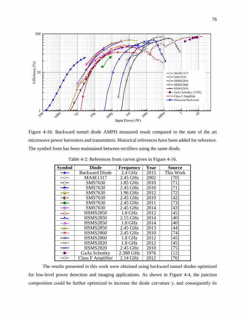
76
Figure 4-16: Backward tunnel diode AMPH measured result compared to the state of the art
microwave power harvesters and transmitters. Historical references have been added for reference.
The symbol form has been maintained between rectifiers using the same diode.
Table 4-2: References from curves given in Figure 4-16.
Symbol Diode Frequency Year Source Backward Diode 2.4 GHz 2015 This Work MA4E1317 2.45 GHz 2002 [70] SMS7630 1.85 GHz 2010 [71] SMS7630 2.45 GHz 2010 [71] SMS7630 1.96 GHz 2012 [72] SMS7630 2.45 GHz 2010 [42] SMS7630 2.45 GHz 2011 [73] SMS7630 2.45 GHz 2014 [43] HSMS2850 1.8 GHz 2012 [45] HSMS2850 2.15 GHz 2014 [40] HSMS2850 1.8 GHz 2014 [40] HSMS2850 2.45 GHz 2013 [44] HSMS2860 2.45 GHz 2010 [74] HSMS2860 1.8 GHz 2012 [45] HSMS2820 1.8 GHz 2012 [45] HSMS2820 2.45 GHz 2010 [75] GaAs Schottky 2.388 GHz 1976 [12] Class F Amplifier 2.14 GHz 2012 [76]
The results presented in this work were obtained using backward tunnel diodes optimized
for low-level power detection and imaging applications. As shown in Figure 4-4, the junction
composition could be further optimized to increase the diode curvature γ, and consequently its

77
current responsivity ℜI0, increasing the power conversion efficiency even more at lower input
powers. The diode junction area, on the other hand, could be increased to optimize Rj0, which could
be used to minimize matching losses, although this would also increase the junction capacitance
Cj. The authors believe this increase in Cj would not be large enough to impact significantly
performance in AMPH applications, since the frequencies of signals where higher power density
appear are usually below 3 GHz [3, 6]. The expected improvements in AMPH for a varying
backward tunnel diode anode Al composition are shown in Figure 4-17; this efficiency
improvement was calculated using the simulation results given in Figure 4-4 adjusting the junction
area so that a 12.5 kΩ Rj0 was maintained. The intrinsic capacitance value remains negligible at
2.45 GHz even with an increasing anode Al composition. As a result, the power conversion
efficiency is improving in the same exponential fashion as the curvature γ. This low power analysis
forecasts a significant improvement of at least one order of magnitude on the efficiency for
narrower tunneling window. Determining and verifying the optimum characteristics of a backward
tunnel diode for AMPH remains the subject of future work.
Figure 4-17: Expected power conversion efficiency improvement for different backward tunnel
diode anode Al compositions, the diode junction area was calculated to mantain a 12.5 kΩ
junction resistance.

78
4.2.8 Acknowledgment
The authors would like to thank Rogers Corporation for providing the laminates used in
this project.
The authors would also like to thank the support provided by the Poly-GRAMES Research
Center technical support team, who are: Traian Antonescu, Steve Dubé, Maxime Thibault, and
Jean-Sébastien Décarie.
79
CHAPITRE 5 TRANSMISSION DE PUISSANCE PAR ONDES
MILLIMETRIQUES (94 GHz)
5.1 Introduction
A la différence de la récupération d’énergie des radiofréquences ambiantes, qui peut être
utilisée dans les applications avec une très faible consommation d’énergie, la transmission de
puissance par micro-ondes ou même ondes millimétriques peut être utilisée dans des applications
dans lesquelles le dispositif a besoin d’une puissance dans une plage allant des microwatts jusqu’à
quelques watts; et qui requièrent également une source de puissance sans fil, petite et légère.
Dans le schéma classique de transmission de puissance sans fil un émetteur est
intentionnellement installé pour augmenter la densité de puissance disponible pour le circuit de
récupération d’énergie micro-ondes, ce qui permet que de plus hautes puissances soient fournies
par le circuit de redressement de puissance. Les premières démonstrations de transmission de
puissances par micro-ondes ont été effectuées par Brown et Dickinson dans les décennies de 1960
et de 1970, où jusqu’à 30 kW cc ont été récupérés par un lien de transmission de puissance par
micro-ondes [11, 12].
Ce travail qui est présenté dans la suite sous le format d’article, explore l’application de la
transmission de puissance par micro-ondes pour résoudre un des problèmes classiques de la
conception des micro-robots : la disponibilité d’une source d’énergie fiable et de taille et poids
compatibles avec les dimensions d’un micro-robot.
Les micro-robots peuvent être utilisés dans une multitude de scénarios. Mentionnons les deux
exemples importants de la décontamination de régions affectées par un débordement de produits
chimiques ou la fouille de décombres après un séisme ou une autre catastrophe. Dans ces deux
exemples, la région affectée pourrait être illuminée par une source de micro-ondes, qui fournirait
ainsi la puissance aux micro-robots dotés d’une rectenne.
Dans ce travail une rectenne a été développée à la fréquence de 94 GHz. A cette fréquence la
longueur d’onde dans le vide est de seulement 3.19 mm, ce qui permet la conception d’une rectenne
de dimensions très réduites. Un circuit d’adaptation d’impédances a été réalisé en technologie de
guide d’ondes coplanaire, de façon à simplifier la connexion à l’antenne papillon à fentes qui a été

80
choisie en raison de sa caractéristique large bande et qui peut accommoder ainsi une variation de
dimensions dues aux imprécisions de la fabrication. Cette antenne a aussi été sélectionnée pour son
patron de rayonnement ayant une faible directivité, caractéristique nécessaire pour l’application
micro-robots, puisque la position du micro-robot par rapport à la source de puissance est variable.
Toutes les simulations du circuit d’adaptation d’impédances ont été faites utilisant les logiciels
HFSS pour les lignes de transmission et Keysight ADS pour les effets non linéaires. L’antenne a
été développée avec le logiciel HFSS.
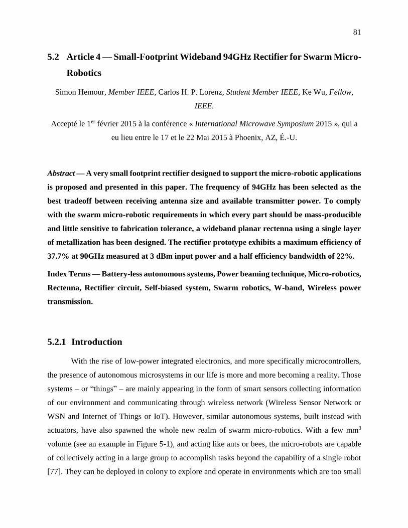
81
5.2 Article 4 — Small-Footprint Wideband 94GHz Rectifier for Swarm Micro-
Robotics
Simon Hemour, Member IEEE, Carlos H. P. Lorenz, Student Member IEEE, Ke Wu, Fellow,
IEEE.
Accepté le 1er février 2015 à la conférence « International Microwave Symposium 2015 », qui a
eu lieu entre le 17 et le 22 Mai 2015 à Phoenix, AZ, É.-U.
Abstract — A very small footprint rectifier designed to support the micro-robotic applications
is proposed and presented in this paper. The frequency of 94GHz has been selected as the
best tradeoff between receiving antenna size and available transmitter power. To comply
with the swarm micro-robotic requirements in which every part should be mass-producible
and little sensitive to fabrication tolerance, a wideband planar rectenna using a single layer
of metallization has been designed. The rectifier prototype exhibits a maximum efficiency of
37.7% at 90GHz measured at 3 dBm input power and a half efficiency bandwidth of 22%.
Index Terms — Battery-less autonomous systems, Power beaming technique, Micro-robotics,
Rectenna, Rectifier circuit, Self-biased system, Swarm robotics, W-band, Wireless power
transmission.
5.2.1 Introduction
With the rise of low-power integrated electronics, and more specifically microcontrollers,
the presence of autonomous microsystems in our life is more and more becoming a reality. Those
systems – or “things” – are mainly appearing in the form of smart sensors collecting information
of our environment and communicating through wireless network (Wireless Sensor Network or
WSN and Internet of Things or IoT). However, similar autonomous systems, built instead with
actuators, have also spawned the whole new realm of swarm micro-robotics. With a few mm3
volume (see an example in Figure 5-1), and acting like ants or bees, the micro-robots are capable
of collectively acting in a large group to accomplish tasks beyond the capability of a single robot
[77]. They can be deployed in colony to explore and operate in environments which are too small
82
or too dangerous for people or larger robots, e. g. search and rescue in earthquake rubble, bomb
disposal, inspection of radioactive hardware, etc.
Like their sensor-oriented counterparts, robotic autonomous microsystems cannot rely only
on batteries, which would be incompatible with their size and life-span requirements. Instead,
remote or wireless powering is needed to offer the flexibility to relocate the source of energy.
Energy harvesting [13], however, would not match the degree of reliability required by the duties
of micro-robots. Wireless power transmission technology, based on resonant magnetic coupling, is
also to be avoided because of the poor distance-to-resonator diameter ratio [49]. Thus, and since
many materials found in nature are opaque to light, the best choice tends to be found in millimeter-
wave and sub-THz region.
Figure 5-1: (a) Photograph of the I-SWARM micro-robot [77], (b) Proposed 94GHz rectenna.
5.2.2 Choice of Frequency and Technology
The technology that is usually chosen for the micro-robotics should comply with
elementary requirements: every part of the robots should be easy-to-manufacture and accept a high-
degree fabrication tolerance to enable mass-production.
In a tradeoff between receiving antenna size and ability to generate a high power at the
transmitter, the 94GHz frequency of operation was selected. A wireless power beaming platform
(Figure 5-2) with a 100W Klystron amplifier, which would be eventually used to evaluate energy
transfer over distance, was built.
There are few works of rectifier reported in the literature working in the upper millimeter
band, all using CMOS technology. In [78], an 8% RF-to-DC rectification efficiency has been
obtained at 71GHz for 5 dBm input power. In [79], a 10% efficiency has been obtained at 94GHz

83
for 4.5 dBm input power. Both works used 65cm(1) CMOS technology. In this work, a millimeter-
wave GaAs Schottky diode (Virginia diode VDI ZBD) is selected to design the proposed 94GHz
rectifier energy receiver. It is expected that this diode, which was especially developed to operate
above 100GHz would outclass CMOS rectifiers, especially bellow 1mW RF power.
Figure 5-2: 94GHz power beaming platform. (1) 18.8GHz signal generator, (2) power meter, (3)
frequency quintupler, (4) variable attenuators, (5) 100W 50dB gain klystron amplifier, (6) high
voltage Klystron power supply, (7) coupler & power probe, (8) WR10 power load, (9) 43dB gain
cassegrain antenna, (10) chiller and cooling systems
5.2.3 Rectenna Development
The topology of the proposed rectenna is depicted in Figure 5-3. Coplanar waveguide
(CPW) technology is selected for its simple fabrication process.
1 L'unité appropriée est nm, cependant le texte originel tel quel publié dans la conférence a été maintenu selon requis
par le règlement de l’École Polytechnique de Montréal pour les mémoires écrites par articles.

84
Figure 5-3: Schematic of the proposed 94GHz rectenna. The antenna is modeled as a Thevenin
source, VA and RA being respectively the equivalent RF source and impedance of the antenna. LT
and CT are the inductance and capacitance accounting for effects of the pad and mounting. LS and
CP are roughly the packaging parasitics, while RS, the series resistance, and CJ0 are dependent on
the junction properties.
5.2.3.1 Antenna design
A CPW-fed bow-tie slot antenna is selected and designed using Ansoft HFSS to receive the
power beam. This type of antenna is rather large-band, which allows for good fabrication
tolerances. A set of Inter Digital Capacitors at each side of the bow-tie slot is utilized to open the
DC current path and include the load. As it is found in the literature [80] and verified in Figure 5-4
(b), planar antenna on high permittivity substrate tends to radiate naturally through its dielectric.
The antenna is designed with a single lobe, but as it can be seen in the radiation pattern in Figure
5-4 (b), the presence of the diode and its matching network have broken the symmetry of the whole
rectenna, giving rise to a second lobe. This is not a critical problem, as it adds a second direction
of transmission, which may be usefull in our application, and we are not restricted by the amount
of power density available at the receiving antenna.
5.2.3.2 Diode model extraction
Prior to the design, a diode sample mounted using conductive epoxy (Epo-Tech H20) on a
CPW line has been characterized, the used substrate was 10mil alumina. The obtained scattering
parameters have been de-embedded after a TRL calibration. Figure 5-3 shows a set of parasitic
elements extracted from the mounted diode characterization. DC characterization of the I(V) curve
enabled the recovery of the Shockley diode parameters (Table 5-1). The junction diode’s large
signal model is modeled with RJ0.

85
Figure 5-4: Simulation results of full-wave FDTD analysis (a) Surface losses on the rectenna in
W/m² and (b) Radiation pattern of the entire rectenna (antenna & rectifier)
5.2.3.3 Rectifier circuit
A single diode topology is selected over a dual diode structure [81] or full bridge
architecture [82] to reduce effects of the parasitics and size. A taper has to be included in the
matching circuit, as the width of the Schottky diode die is larger than the CPW feed of the antenna.
The matching network transforms the 50Ohm real impedance of the antenna into the expected 108-
j11 Ohm of the diode. Figure 5-4 shows the surface losses in the rectenna. It can be seen that the
losses originate mainly from the matching network. The matching efficiency computed from
Harmonic Balance simulation is 65% at -10 dBm and 67.5% at -5 dBm input power levels.
86
Table 5-1: Diode parameters extracted from RF and DC measurements
Is Vj N Ibv Rs Cj0
Value 5x10⁻⁶ A 0.085 V 1.1 0.1 mA 13 Ω 19 fF
5.2.4 Measurements
As it is discovered, the fabrication process in our work has introduced a 4 µm over-etching.
It is seen in Figure 5-5 that the antenna resonance frequency is moved from 94GHz to 90GHz. The
over-etching might tend to reduce the matching efficiency because of higher radiation losses
although this effect is hard to quantify in our measurements.
Figure 5-5: Comparison of simulation and measurement for S11 of the CPW-fed bow-tie antenna.
Measurements were performed on a probe station after on-wafer Short-Open-Load calibration.
On-wafer measurements were done using a power calibrated procedure at the tips of the
GSG probe [9]. A comparison of the simulated and measured rectifier circuit (without the antenna)
behavior is plotted in Figure 5-6, given for an input power of -12 dBm. It suggests that in our
simulation, parasitic components of the diode are overestimated, thus leading to an underestimated
power conversion efficiency. In the measurement, the rectifier current is larger than expected, and
in turn decreases the junction resistance, which explains why the optimum resistance is larger in
the simulation than in the measurement. The frequency shift caused by the over etching is also
clearly visible. The robustness of the circuit to fabrication tolerance, provided by a wideband circuit
87
design, is also demonstrated: Even under the over etching condition, the rectifier is still operating
at 94GHz with almost 7% efficiency.
Figure 5-6: Rectifier efficiency as a function of frequency, plotted with the optimum load for an
input power of -12 dBm (calibrated probe measurement). In the simulation condition, the
optimum load was found to be 600 Ohm (solid line). However, due to lower parasitic in the real
diode, junction current has been higher in the measurement, leading to a lower junction
resistance, thus to a lower optimum load resistance, i.e. 400 Ohm (dotted line).
Figure 5-7: Rectifier efficiency as a function of the input power at 90GHz and 94GHz (calibrated
probe measurement at the input of the rectifier circuit). The optimum resistive load is indicated
for each measurement point. In the insert, the efficiency is shown as a function of DC current, for
a RF signal of 3 dBm at 90GHz.

88
A comparison between the optimum rectification frequency, 90GHz, and 94GHz is
presented in Figure 5-7, showing the benefit of the wideband design on the behavior of the rectifier
circuit (no antenna) fabricated with a high tolerance, In Table 5-2 the results are summarized and
compared with the previous works. The efficiency is improved by nearly four times, for a similar
half efficiency bandwidth.
Table 5-2: Comparison with other related works
[78] [79] This work
Technology 65nm CMOS 65nm CMOS GaAs Schottky diode
Frequency 70-72GHz 94GHz 94GHz
Rectifier efficiency 8% (71GHz) 10% 37.7% (90GHz)
32.3% (94GHz)
Half efficiency Bandwidth
- 24%* 22%
Input power 5 dBm 4.5 dBm 3 dBm
Rectifier area 1.09mm2 0.095mm2 1.17mm2
Rectenna area 1.78mm2 0.48mm2 5.62mm2 * Simulation results
5.2.5 Conclusion
We have developed a rectifier compatible with mass-production requirement and high
fabrication tolerance (Half efficiency bandwidth of 22%). An unprecedented efficiency of 37.7%
has been obtained at 90GHz. The rectifier presented in this work is the first iteration in our research.
A further improvement includes lower area, improved efficiency using higher Schottky barrier
diode, such as mixer diode, and circuit engineering in order to obtain a necessary amount of voltage
to operate the microrobot of interest.
5.2.6 Acknowledgement
The authors would like to acknowledge the financial support of the Natural Sciences and
Engineering Research Council of Canada (NSERC) and CREATE PERSWADE Training Program,
which partially funded the work presented in this article. The authors wish to thank J. Gauthier, M.
Thibault, D. Dousset, S. Dubé, T. Antonescu, and J.-S. Décarie, all with the Poly-Grames Research
Center, École Polytechnique de Montréal, Montreal, QC, Canada, for their technical assistance.

89
CHAPITRE 6 DISCUSSION GÉNÉRALE
La récupération d’énergie micro-ondes ambiantes demeure un défi en raison des faibles
densités de puissance disponibles dans l’environnement, comme rapporté par des études déjà
publiées [3, 6, 8]. Dans ce travail on a présenté un modèle mathématique qui permet la
compréhension des mécanismes de redressement et des pertes lors de la conversion de puissance
micro-ondes en courant continu (cc). À partir de la théorie développée pour établir ce modèle, deux
méthodes ont été proposées et vérifiés pour augmenter l’efficacité de conversion de puissance
micro-ondes en cc dans les faibles puissances: la récupération hybride coopérative d’énergie
ambiante, présentée dans le chapitre 3, et l’utilisation des diodes tunnel avec une forte responsivité
en courant démontrée dans le chapitre 4.
Toutefois, la perte dans le réseau d’adaptation d’impédance reste un phénomène majeur à
l’origine de la faible ECP obtenue dans les circuits de récupération d’énergie micro-ondes
ambiantes. Dans le chapitre 4, nous avons vu que pour une puissance d’entrée de -40 dBm,
l’efficacité atteignable sans pertes d’adaptation était estimé à 15%, alors que les mesures ont
montré une efficacité proche de 4.2%. Le même effet a été constaté pour une puissance à l’entrée
de -30 dBm, où le maximum atteignable était estimé à 36% et les mesures ont démontré une ECP
proche de 18%. Les résultats présentés dans le chapitre 2 mettent cet effet en évidence dans la
Figure 2-7, où il existe une résistance de jonction Rj0 optimale dans un compromis entre les pertes
d’insertion du réseau d’adaptation d’impédances et l’efficacité de conversion de puissance micro-
ondes en cc. À ce point de fonctionnement, les pertes d’insertion du réseau d’adaptation
d’impédances sont responsables à hauteur de 30% de la puissance perdue.
Ces pertes importantes dans le réseau d’adaptation d’impédances ont été étudiées dans ce
chapitre avec l’aide du modèle de pertes présenté dans le Chapitre 2. Un modèle de diode à faibles
pertes parasitiques a été utilisé pour étudier une nouvelle topologie de réseau d’adaptation
d’impédances visant diminuer ses pertes d’insertion. Les caractéristiques de la diode sont : Cj0 =
15.7 fF, Cp = 25.2 fF, Rs = 15 Ω, Lp =0 et N=1.1. Le courant de saturation Is a été varié de 10 nA à
100 μA et une capacitance de 10 fF a été ajoutée en parallèle avec la diode pour prendre en compte
la capacitance des plots de soudure. Tous les calculs considèrent des lignes microruban 50 Ω
construites sur un substrat Rogers RT/Duroid 6002 d’une épaisseur de 30 mil.
90
Utilisant l’équation (2-16) pour calculer le facteur de qualité requis pour adapter une diode
non polarisé avec une résistance de jonction égale à 12.5 kΩ à une source de 50 Ω, on obtient Qr =
15.78. Cela veut dire qu’un réseau d’adaptation qui présente un facteur de qualité égal à 15.78
présenterait une perte d’insertion de 50%. Ce facteur de qualité ne semble pas difficile à obtenir ni
même à dépasser, mais comme décrit par l’équation (2-22), la constante effective de pertes d’une
ligne de transmission augmente quand l’onde stationnaire présente sur cette ligne a un ROS
important. En raison de la grande différence entre l’impédance de la source et de la charge
représentée par la diode, cette augmentation dans les pertes sur la ligne de transmission ne peut pas
être négligée.
L’impédance initiale d’une telle diode est proche de l’infini, comme montré dans la Figure 6-1
ici-bas. Cela signifie que le ROS soutenu sur la ligne connectée à cette diode est très élevé.
Figure 6-1: Effet de l’ajout de deux inductances de 34 nH en série avec la diode sur l’impédance
d’entrée. Fréquence = 2.45 GHz.
Une façon de diminuer les pertes d’insertion de ce réseau d’adaptation d’impédances est de
diminuer le ROS présent sur la ligne connectée à la diode. Pour y arriver, il faut rapprocher
l’impédance à adapter du centre de l’abaque de Smith, comme montré dans la Figure 6-1. Dans
cette figure deux inductances de 34 nH Coilcraft (0302CS-34NXJL_) ont été mises en série avec
la diode. Le modèle réel de l’inductance, fourni par Coilcraft, a été utilisé pour prendre en compte
les éléments parasites.
Impédance
initiale
Impédance avec
inductances en série

91
L’effet de l’ajout de ces inductances peut sembler négligeable sur l’abaque de Smith,
cependant le coefficient de réflexion de l’impédance résultante connecté à une ligne de 50 Ω chute
de 0.99 vers 0.925. Cela signifie une chute de 199 à 25.7 dans le ROS et une chute de 99 vers 12.85
dans le facteur de multiplication de l’atténuation de la ligne de transmission selon l’équation (2-
22) soit une atténuation 7.7 fois plus petite. La théorie présentée dans la section 2.1.6 a été utilisée
pour vérifier l’impact de l’ajout d’inductances en série avec la diode, avant de l’adapter à une
source de 50 Ω avec un réseau d’adaptation d’impédances en L, comme montré dans la Figure 2-
7. Les ECP calculées avec la méthode présentée dans le chapitre 2 sont données dans la Figure 6-2
ici-bas :
Figure 6-2: ECP calculée avec le modèle présenté dans le chapitre 2. D’inductances ont été mises
en série avec la diode. La puissance à l’entrée est de -30 dBm, Fréquence = 2.45 GHz.
On voit que l’ajout des inductances permet d’augmenter l’ECP maximale qui peut être
obtenue. L’ajout des inductances diminue le coefficient de réflexion au bout de la ligne de
transmission série utilisée dans le réseau d’adaptation d’impédances en L, cela réduit les pertes
totales dans le réseau d’adaptation d’impédances composé des inductances plus les lignes micro-
ruban en L, selon la théorie présentée dans 2.2.6. L’ECP maximale monte de 22.5% pour le réseau
sans inductances à 35% pour le réseau avec 3 inductances en série. L’ajout de plus de 3 inductances
diminue l’ECP maximale en raison des pertes provenant de la résistance série des inductances, dans
ce point, un équilibre est atteint entre la diminution du ROS sur la ligne connectée aux inductances
et diode, et les pertes introduites par les inductances.
92
Une deuxième remarque qui peut être faite à partir des données de la Figure 6-2 est la
différence de seulement 4% qu’apparaît entre les résultats simulés dans Keysight ADS et calculés
pour le circuit sans diodes en série, ce qui est un très bon accord considérant les simplifications de
la méthode analytique proposée.
Cette méthode a été utilisée pour améliorer la rectenne présentée dans le chapitre 4, où
l’utilisation d’une diode tunnel avec une haute responsivité en courant a été étudiée pour augmenter
l’ECP maximale des circuits de récupération d’énergie ambiante. Selon les simulations réalisées
dans le logiciel Keysight ADS, l’ajout de deux inductances en série avec la diode (Coilcraft
03CS21N et 03CS8N3) permettrait d’augmenter l’ECP atteignable. Le circuit a été simulé avec
l’aide de l’outil Momentum, lequel a été utilisé pour obtenir les paramètres S du circuit par la
méthode des moments. Ces résultats ont été utilisés avec la simulation d’équilibrage harmonique
pour obtenir l’ECP du circuit proposé. La topologie finale du circuit proposé est donnée dans la
Figure 6-3 (Plan de masse sur la face opposée de la carte de circuit imprimée).
Figure 6-3: Topologie finale du circuit proposé avec le but de diminuer les pertes d’insertion du
rectifieur présenté dans le chapitre 4.
Le résultat de la simulation est comparé à l’ECP maximale prévue et les résultats des
mesures présentées dans l’article du chapitre 4. La méthode proposée donne un circuit qui présente
de très faibles pertes d’insertion pour le réseau d’adaptation d’impédances. L’ECP prévu est proche
du maximum atteignable, comme montré dans la Figure 6-4.
Sortie cc
Entrée Micro-
Ondes Diode Inductances
Réseau en L
Court-Circuit
ajustable
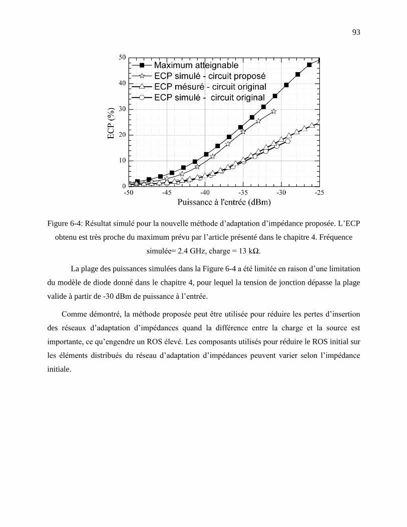
93
Figure 6-4: Résultat simulé pour la nouvelle méthode d’adaptation d’impédance proposée. L’ECP
obtenu est très proche du maximum prévu par l’article présenté dans le chapitre 4. Fréquence
simulée= 2.4 GHz, charge = 13 kΩ.
La plage des puissances simulées dans la Figure 6-4 a été limitée en raison d’une limitation
du modèle de diode donné dans le chapitre 4, pour lequel la tension de jonction dépasse la plage
valide à partir de -30 dBm de puissance à l’entrée.
Comme démontré, la méthode proposée peut être utilisée pour réduire les pertes d’insertion
des réseaux d’adaptation d’impédances quand la différence entre la charge et la source est
importante, ce qu’engendre un ROS élevé. Les composants utilisés pour réduire le ROS initial sur
les éléments distribués du réseau d’adaptation d’impédances peuvent varier selon l’impédance
initiale.

94
CHAPITRE 7 CONCLUSION ET TRAVAUX FUTURES
Ce travail a exploré la récupération d’énergie micro-ondes ambiante (REMA), débutant par la
présentation d’un modèle mathématique où les mécanismes des pertes et de conversion d’énergie
micro-ondes en courant continu par un circuit de redressement à diodes sont expliqués. L’efficacité
totale de conversion de puissance micro-ondes en cc est divisée dans 𝞰m, l’efficacité du réseau
d’adaptation d’impédances, 𝞰p, l’efficacité parasitique de la diode, 𝞰RFDC, l’efficacité de
conversion d’énergie micro-ondes en cc de la jonction non-linéaire et 𝞰SL, l’efficacité de
transfert de puissance de la source à la charge. Chaque efficacité est évaluée
indépendamment et une méthode est proposée pour prédire l’efficacité de chaque étape. Les
résultats prévus par les équations proposées ont été vérifiés et comparés aux résultats mesurés pour
trois prototypes présentés dans le Chapitre 2, y incluant les pertes d’insertion calculées pour le
réseau d’adaptation d’impédances.
La théorie développée pour prévoir les pertes d’insertion du réseau d’adaptation d’impédances
peut facilement être utilisée pour d’autres applications où une grande différence entre l’impédance
de la source et de la charge peut engendrer de pertes d’insertion importantes dans le circuit
d’adaptation, comme dans la récupération d’énergie micro-ondes ambiante. La solution analytique
peut facilement être mise en œuvre dans un logiciel de résolution d’équations mathématiques
comme MATLAB, pour aider à choisir la topologie qui présente la plus faible perte par moyen de
la méthode analytique avant de réaliser la simulation électromagnétique du circuit imprimé,
laquelle peut être utilisée pour optimiser le réseau d’adaptation choisi.
Le modèle mathématique a amené à deux méthodes possibles pour augmenter l’ECP dans la
plage de puissances en-dessous de -30 dBm, comme c’est généralement lecas dans les applications
de REMA. La première méthode, présentée dans le chapitre 3, combine la puissance provenant de
plusieurs sources dans un seul élément non-linéaire utilisé pour le redressement. Dans le travail
présenté, la puissance micro-ondes reçue à 2.1 GHz a été combinée avec la puissance récupérée
d’une source de vibration mécanique. L’ECP a été doublée pour des puissances à l’entrée en-
dessous de -40 dBm pour chaque source, ce qui quadruplait la puissance totale récupérée par le
circuit par rapport à une rectenne simple. Cette avantage diminuait progressivement pour une
puissance d’entrée montant jusqu’à -24 dBm, point où la puissance perdue dans les produits
d’intermodulation entre les signaux d’entrée égalait les gains de la méthode collaborative hybride
95
proposée. Un autre avantage de la méthode proposée est la combinaison des puissances récupérées
directement par le dispositif non-linéaire utilisé dans le redressement, sans le besoin d’un circuit
supplémentaire pour réaliser cette fonction, lequel rendrait le système moins efficace et
augmenterait les coûts et complexité du circuit.
Ensuite, une deuxième méthode pour augmenter l’ECP a été évaluée : l’utilisation des diodes
tunnel avec une responsivité en courant à zéro-biais plus élevée que celle atteignable avec les
diodes Schottky, laquelle a un maximum égal à 19.4 A/W à la température ambiante. Des
échantillons de diodes tunnel ayant une responsivité en courant mesurée proche de 22 A/W en
température ambiante ont étés caractérisés et un modèle de diode a été créé dans le logiciel
Keysight ADS. Ayant le modèle de diode en main, des prototypes ont étés construits et mesurés.
L’ECP mesurée a atteint 18.2% pour une puissance de -30 dBm à l’entrée du redresseur, soit un
gain de 3.6 fois par rapport au meilleur résultat publié pour les circuits de récupération de puissance
micro-ondes ambiantes fonctionnant à de puissances et fréquences similaires avec des diodes
Schottky. Lorsque comparé au meilleur résultat présenté dans le chapitre 2, obtenu du circuit
construit avec les diodes VDI W-Band ZBD, le gain était de 1.67, ce qui peut être justifié par les
très faibles pertes parasitiques présentes dans cette dernière diode. Ce chiffre est aussi en accord
avec le gain prédit par le modèle mathématique si on considère que les pertes dans le réseau
d’adaptation, les pertes parasitiques et les pertes dans le transfert source – charge sont proches pour
les deux diodes. Selon l’équation (2-11) l’efficacité de conversion d’énergie micro-ondes en cc est
proportionnelle au carré de la responsivité en courant à zéro-biais. Vu que 𝕽I0 pour la diode VDI
est de 17.6 A/W, le gain calculé attendu est égal à :
2
2
221.56
17.6Gain (7.1)
un résultat très proche de celui mesuré considérant l’approximation faite quand on a considéré que
les autres pertes sont identiques pour les deux diodes. Comme montré dans la Figure 4-17 ce gain
peut encore être amélioré significativement en changeant la composition de l’anode de la diode
tunnel, la confirmation expérimentale de cette prévision reste encore comme un des travaux futurs
proposés par ce mémoire.
Finalement, un circuit de transmission de puissance par micro-ondes a été présenté. La
transmission de puissance a lieu dans une plage de puissances plus élevée que la REMA et peut

96
être utilisée dans les applications où la charge a besoin des puissances plus élevées pour
fonctionner. Dans ce travail une rectenne de dimensions et taille réduites a été proposée pour être
utilisée comme source de puissance pour des micro-robots. Un prototype a été construit et mesuré
à 94 GHz, lequel a été présenté dans le Chapitre 5.
Une faiblesse toutefois a été remarquée pour tous les circuits présentés dans ce travail et aussi
dans les résultats présentés dans l’état de d’art trouvé dans les derniers articles publiés dans le
domaine de la REMA. Comme présenté dans les Chapitres 2 et 4, entre 30% et 50% de la puissance
reçue est dissipée dans le circuit d’adaptation d’impédances. Dans le chapitre 6 une étude est
présentée où l’origine de ces pertes et un moyen pour les réduire sont discutés. Le gain attendu
pour le circuit proposé dans le Chapitre 4 a été présenté dans la Figure 6-4, où on voit une hausse
de l’efficacité de conversion de puissance à -30 dBm de 18.2% à 31%, très proche du maximum
atteignable pour le cas d’un réseau d’adaptation d’impédances sans pertes, égal à 38%. La
technique appliquée pour cet exemple pourrait aussi être utilisée pour les circuits présentés dans le
Chapitre 2 de façon à augmenter les ECP obtenus. La vérification des résultats prévus par la
construction des prototypes est proposée comme un des travaux futurs à réaliser.
Une dernière vérification proposée est l’étude de l’effet des pertes ohmiques et diélectriques
sur le modèle d’estimation de αr, la constante d’atténuation équivalente pour une ligne de
transmission sur laquelle des ondes stationnaires sont présentes. L’évaluation indépendante des
pertes ohmiques et diélectriques dans le modèle présenté dans le chapitre 2, section 2.1.6, reste
encore à être faite. Dans le développement du modèle seulement le rapport d’onde stationnaire en
tension a été considéré de façon générale pour corriger la constante d’atténuation totale de la ligne.
Toutefois une constante d’atténuation équivalente plus précise, en prenant en compte les effets
d’ondes stationnaires sur les constantes de pertes ohmiques αc et diélectriques αd séparément, qui
ensemble composent la constante d’atténuation de la ligne de transmission α, reste encore à être
étudiée.
Ce mémoire de maîtrise a exploré avec succès les fondements de la récupération d’énergie
micro-ondes ambiante. Un modèle mathématique a été proposé et vérifié. À partir de la théorie
décrite, deux méthodes ont étés proposées pour augmenter l’efficacité de conversion de puissance
des circuits de récupération d’énergie ambiante. La vérification de ces méthodes par les prototypes

97
développés a confirmé l’efficacité de ces deux méthodes dans la plage de puissance où la REMA
fonctionne.
98
RÉFÉRENCES
[1] J. Gubbi, R. Buyya, S. Marusic, and M. Palaniswami, "Internet of Things (IoT): A vision,
architectural elements, and future directions," Future Generation Computer Systems, vol.
29, pp. 1645-1660, 2013.
[2] D. Miorandi, S. Sicari, F. De Pellegrini, and I. Chlamtac, "Internet of things: Vision,
applications and research challenges," Ad Hoc Networks, vol. 10, pp. 1497-1516, 2012.
[3] F. Giuppi, K. Niotaki, A. Collado, and A. Georgiadis, "Challenges in energy harvesting
techniques for autonomous self-powered wireless sensors," in Microwave Conference
(EuMC), 2013 European, 2013, pp. 854-857.
[4] M. K. Hosain, A. Z. Kouzani, M. F. Samad, and S. J. Tye, "A Miniature Energy Harvesting
Rectenna for Operating a Head-Mountable Deep Brain Stimulation Device," Access, IEEE,
vol. 3, pp. 223-234, 2015.
[5] K. Niotaki, F. Giuppi, A. Georgiadis, and A. Collado, "Solar/EM energy harvester for
autonomous operation of a monitoring sensor platform," Wireless Power Transfer, vol. 1,
pp. 44-50, 2014.
[6] M. Pinuela, D. C. Yates, S. Lucyszyn, P. D. Mitcheson, C. Wang, F. Hu, et al. (2012,
14/06/2014). London RF Survey. Available: http://www.londonrfsurvey.org/
[7] M. Pinuela, P. D. Mitcheson, and S. Lucyszyn, "Ambient RF Energy Harvesting in Urban
and Semi-Urban Environments," IEEE Transactions on Microwave Theory and
Techniques, vol. 61, pp. 2715-26, 2013.
[8] K. Sangkil, R. Vyas, J. Bito, K. Niotaki, A. Collado, A. Georgiadis, et al., "Ambient RF
Energy-Harvesting Technologies for Self-Sustainable Standalone Wireless Sensor
Platforms," Proceedings of the IEEE, vol. 102, pp. 1649-1666, 2014.
[9] S. Hemour, Y. P. Zhao, C. H. P. Lorenz, D. Houssameddine, Y. S. Gui, C. M. Hu, et al.,
"Towards Low-Power High-Efficiency RF and Microwave Energy Harvesting," IEEE
Transactions on Microwave Theory and Techniques, vol. 62, pp. 965-976, Apr 2014.
[10] C. H. P. Lorenz, S. Hemour, W. Li, Y. Xie, J. Gauthier, P. Fay, et al., "Overcoming the
Efficiency Limitation of Low Microwave Power Harvesting with Backward Tunnel Diodes
" in Microwave Symposium (IMS), 2015 IEEE MTT-S International, Phoenix, AZ, USA,
2015, pp. 1-4.
[11] W. C. Brown, "Experimental airborne microwave supported platform," Rome Air
Development Center, Rome, NY 1965.
[12] R. M. Dickinson, "Performance of a high-power, 2.388-GHz receiving array in wireless
power transmission over 1.54 km," in 1976 IEEE MTT-S International Microwave
Symposium, 14-16 June 1976, New York, NY, USA, 1976, pp. 139-41.
[13] S. Hemour and K. Wu, "Radio-Frequency Rectifier for Electromagnetic Energy
Harvesting: Development Path and Future Outlook," Proceedings of the Ieee, vol. 102, pp.
1667-1691, Nov 2014.
99
[14] J. G. Koomey, S. Berard, M. Sanchez, and H. Wong, "Implications of Historical Trends in
the Electrical Efficiency of Computing," Annals of the History of Computing, IEEE, vol.
33, pp. 46-54, 2011.
[15] J. G. Koomey, H. S. Matthews, and E. Williams, "Smart everything: Will intelligent
systems reduce resource use?," Annual Review of Environment and Resources, vol. 38, p.
311, 2013.
[16] Libelium. (2015, 15/06/2015). 50 Sensor Applications for a Smarter World. Available:
http://www.libelium.com/top_50_iot_sensor_applications_ranking/
[17] T. W. Yoo and K. Chang, "Theoretical and Experimental Development of 10 and 35 Ghz
Rectennas," Ieee Transactions on Microwave Theory and Techniques, vol. 40, pp. 1259-
1266, Jun 1992.
[18] H. C. Torrey, C. A. Whitmer, and S. A. Goudsmit, Crystal rectifiers, 1st ed. New York,:
McGraw-Hill Book Co., 1948.
[19] J. Guo and X. Zhu, "An improved analytical model for RF-DC conversion efficiency in
microwave rectifiers," in 2012 IEEE MTT-S International Microwave Symposium, IMS
2012, June 17, 2012 - June 22, 2012, Montreal, QC, Canada, 2012, pp. 1-3.
[20] Skyworks. (03/03/2015). SMS7630 Datasheet. Available:
www.skyworksinc.com/products_opendocument.asp?did=331
[21] A. M. Niknejad, Electromagnetics for high-speed analog and digital communication
circuits: Cambridge University Press, 2007.
[22] P. Vizmuller, RF design guide: systems, circuits, and equations vol. 1: Artech House, 1995.
[23] A. R. Djordjevic, A. G. Zajic, D. V. Tosic, and T. Hoang, "A note on the modeling of
transmission-line losses," Microwave Theory and Techniques, IEEE Transactions on, vol.
51, pp. 483-486, 2003.
[24] G. L. Ragan, Microwave transmission circuits vol. 9: published and distributed by Boston
Technical Publishers, 1964.
[25] J. E. Zúñiga-Juárez, J. A. Reynoso-Hernández, M. del Carmen Maya-Sánchez, and R. S.
Murphy-Arteaga, "A New Analytical Method to Calculate the Characteristic Impedance
ZC of Uniform Transmission Lines," Computación y Sistemas, vol. 16, pp. 277-285, 2012.
[26] H. W. Bode, Network Analysis and Feedback Amplifier Design: Van Nostrand, 1945.
[27] R. M. Fano, "Theoretical limitations on the broadband matching of arbitrary impedances,"
Journal of the Franklin Institute, vol. 249, pp. 57-83, 1950.
[28] D. M. Pozar, Microwave and RF wireless systems. New York: John Wiley, 2001.
[29] S. A. Maas, Microwave mixers, 2nd ed. Boston, MA: Artech House, 1993.
[30] Infineon. (03/03/2015). BAT15 Datasheet. Available:
http://www.infineon.com/dgdl/Infineon-BAT15SERIES-DS-v01_01-
en.pdf?fileId=db3a304314dca3890114ff6b74ca0b48
[31] Avago. (03/03/2015). HSMS-286X Datasheet. Available:
http://www.avagotech.com/docs/AV02-1388EN
100
[32] Avago. (03/03/2015). HSMS-285X Datasheet. Available:
http://www.avagotech.com/docs/AV02-1377EN
[33] V. Diodes. (03/03/2015). VDI Zero-Bias Detector diode Datasheet. Available:
http://vadiodes.com/images/pdfs/ZBD_20120727_Revision.pdf
[34] J. Hesler and B. Gelmont, "A discussion of power coupling bandwidth limitations of planar
Schottky diodes at submillimeter wavelengths," in Proceedings of the Nineteenth
International Symposium on Space Terahertz Technology, 1998, pp. 173-180.
[35] B. S. Yarman, Design of ultra wideband antenna matching networks : via simplified real
frequency technique. Dordrecht: Springer, 2008.
[36] B. S. Yarman, Design of ultra wideband power transfer networks: John Wiley & Sons,
2010.
[37] R. G. Harrison, "Full nonlinear analysis of detector circuits using Ritz-Galerkin theory," in
Microwave Symposium Digest, 1992., IEEE MTT-S International, 1992, pp. 267-270.
[38] Z. Zhang, R. Rajavel, P. Deelman, and P. Fay, "Sub-Micron Area Heterojunction Backward
Diode Millimeter-Wave Detectors With 0.18 Noise Equivalent Power," Microwave and
Wireless Components Letters, IEEE, vol. 21, pp. 267-269, 2011.
[39] A. Nimo, D. Grgic, T. Ungan, and L. M. Reindl, "A new family of passive wireless RF
harvesters based on R-C-Quartz oscillators," in Microwave Conference (EuMC), 2013
European, 2013, pp. 511-514.
[40] Z. Liu, Z. Zhong, and Y.-X. Guo, "High-efficiency triple-band ambient RF energy
harvesting for wireless body sensor network," in RF and Wireless Technologies for
Biomedical and Healthcare Applications (IMWS-Bio), 2014 IEEE MTT-S International
Microwave Workshop Series on, 2014, pp. 1-3.
[41] C. Valenta and G. Durgin, "Harvesting Wireless Power: Survey of Energy-Harvester
Conversion Efficiency in Far-Field, Wireless Power Transfer Systems," Microwave
Magazine, IEEE, vol. 15, pp. 108-120, 2014.
[42] G. Andia Vera, A. Georgiadis, A. Collado, and S. Via, "Design of a 2.45 GHz rectenna for
electromagnetic (EM) energy scavenging," in Radio and Wireless Symposium (RWS), 2010
IEEE, 2010, pp. 61-64.
[43] W. Haboubi, H. Takhedmit, J.-D. Lan Sun Luk, S.-E. Adami, B. Allard, F. Costa, et al.,
"An Efficient Dual-Circularly Polarized Rectenna for RF Energy Harvesting in the 2.45
GHz Ism Band," Progress In Electromagnetics Research, vol. 148, pp. 31-39, 2014.
[44] B. R. Franciscatto, V. Freitas, J.-M. Duchamp, C. Defay, and T. P. Vuong, "High-efficiency
rectifier circuit at 2.45 GHz for low-input-power RF energy harvesting," in Microwave
Conference (EuMC), 2013 European, 2013, pp. 507-510.
[45] V. Marian, B. Allard, C. Vollaire, and J. Verdier, "Strategy for Microwave Energy
Harvesting From Ambient Field or a Feeding Source," IEEE Transactions on Power
Electronics, vol. 27, pp. 4481-4491, Nov 2012.
[46] G. Marrocco, L. Mattioni, and C. Calabrese, "Multiport sensor RFIDs for wireless passive
sensing of objects—Basic theory and early results," Antennas and Propagation, IEEE
Transactions on, vol. 56, pp. 2691-2702, 2008.

101
[47] J. A. Hagerty, F. B. Helmbrecht, W. H. McCalpin, R. Zane, and Z. B. Popovic, "Recycling
ambient microwave energy with broad-band rectenna arrays," IEEE Transactions on
Microwave Theory and Techniques, vol. 52, pp. 1014-24, 2004.
[48] S. J. Roundy, "Energy scavenging for wireless sensor nodes with a focus on vibration to
electricity conversion," Ph.D. dissertation, Mechanical Engineering, University of
California, Berkeley, 2003.
[49] W. Wang, S. Hemour, and K. Wu, "Coupled resonance energy transfer over gigahertz
frequency range using ceramic filled cavity for medical implanted sensors," Microwave
Theory and Techniques, IEEE Transactions on, vol. 62, pp. 956-964, 2014.
[50] Z. Popovic, "Cut the cord: Low-power far-field wireless powering," Microwave Magazine,
IEEE, vol. 14, pp. 55-62, 2013.
[51] D. Masotti, A. Costanzo, P. Francia, M. Filippi, and A. Romani, "A Load-Modulated
Rectifier for RF Micropower Harvesting With Start-Up Strategies," Microwave Theory and
Techniques, IEEE Transactions on, vol. 62, pp. 994-1004, 2014.
[52] J. Karlovský, "The curvature coefficient of germanium tunnel and backward diodes," Solid-
State Electronics, vol. 10, pp. 1109-1111, 1967.
[53] S. M. Sze and K. K. Ng, Physics of semiconductor devices: John Wiley & Sons, 2006.
[54] C. Burrus, "Backward diodes for low-level millimeter-wave detection," Microwave Theory
and Techniques, IEEE Transactions on, vol. 11, pp. 357-362, 1963.
[55] L. Esaki, "New phenomenon in narrow germanium p− n junctions," Physical Review, vol.
109, p. 603, 1958.
[56] L. Esaki, "Discovery of the tunnel diode," Electron Devices, IEEE Transactions on, vol.
23, pp. 644-647, 1976.
[57] R. Meyers, P. Fay, J. Schulman, S. Thomas III, D. Chow, J. Zinck, et al., "Bias and
temperature dependence of Sb-based heterostructure millimeter-wave detectors with
improved sensitivity," Electron Device Letters, IEEE, vol. 25, pp. 4-6, 2004.
[58] J. Schulman, E. Croke, D. Chow, H. Dunlap, K. Holabird, M. Morgan, et al., "Quantum
tunneling Sb-heterostructure millimeter-wave diodes," in Electron Devices Meeting, 2001.
IEDM'01. Technical Digest. International, 2001, pp. 35.1. 1-35.1. 3.
[59] H. Moyer, J. Schulman, J. Lynch, J. Schaffner, M. Sokolich, Y. Royter, et al., "W-band Sb-
diode detector MMICs for passive millimeter wave imaging," Microwave and Wireless
Components Letters, IEEE, vol. 18, pp. 686-688, 2008.
[60] N. Su, R. Rajavel, P. Deelman, J. N. Schulman, and P. Fay, "Sb-heterostructure millimeter-
wave detectors with reduced capacitance and noise equivalent power," Electron Device
Letters, IEEE, vol. 29, pp. 536-539, 2008.
[61] J. J. Lynch, H. P. Moyer, J. H. Schaffner, Y. Royter, M. Sokolich, B. Hughes, et al.,
"Passive millimeter-wave imaging module with preamplified zero-bias detection,"
Microwave Theory and Techniques, IEEE Transactions on, vol. 56, pp. 1592-1600, 2008.
[62] J. Schulman and D. Chow, "Sb-heterostructure interband backward diodes," Electron
Device Letters, IEEE, vol. 21, pp. 353-355, 2000.

102
[63] N. Su, Y. Tang, Z. Zhang, T. Kuech, and P. Fay, "Observation and control of
electrochemical etching effects in the fabrication of InAs∕ AlSb∕ GaSb heterostructure
devices," Journal of Vacuum Science & Technology B, vol. 26, pp. 1025-1029, 2008.
[64] M. Shams, I. Bin, Y. Xie, Y. Lu, and P. Fay, "An accurate interband tunneling model for
InAs/GaSb heterostructure devices," physica status solidi (c), vol. 10, pp. 740-743, 2013.
[65] Keysight. (2002, 29/06/2015). [VBA Sample Program] Adapter Characterization. User
Manual No. 16000-95024. Available:
http://www.keysight.com/main/editorial.jspx?cc=VN&lc=vie&ckey=85082&nid=-
11143.0.00&id=85082
[66] Agilent. (29/06/2015). Measuring Noninsertable Devices. Product Note No. 8510-13.
Available: http://cp.literature.agilent.com/litweb/pdf/5956-4373E.pdf
[67] J. Randa, W. Wiatr, and R. L. Billinger, "Comparison of adapter characterization methods,"
Microwave Theory and Techniques, IEEE Transactions on, vol. 47, pp. 2613-2620, 1999.
[68] C. H. P. Lorenz, S. Hemour, and K. Wu, "Modeling and Influence of Matching Network
Insertion Losses on Ambient Microwave Power Harvester," presented at the Conference on
Numerical Electromagnetic and Multiphysics Modeling and Optimization (NEMO), 2015
IEEE MTT-S International, Ottawa (ON) Canada, 2015.
[69] A. Dolgov, R. Zane, and Z. Popovic, "Power management system for online low power RF
energy harvesting optimization," Circuits and Systems I: Regular Papers, IEEE
Transactions on, vol. 57, pp. 1802-1811, 2010.
[70] Y.-H. Suh and K. Chang, "A high-efficiency dual-frequency rectenna for 2.45- and 5.8-
GHz wireless power transmission," IEEE Transactions on Microwave Theory and
Techniques, vol. 50, pp. 1784-1789, 2002.
[71] C. M. Ghiglino, "Ultra-wideband (UWB) rectenna design for electromagnetic energy
harvesting," Masters theses, Dept. Teoria del Senyal i Comun., Escola Técnica Superior
d’Enginyeria de Telecomun. de Barcelona, Catalunya, Spain, 2010.
[72] E. Falkenstein, M. Roberg, and Z. Popović, "Low-power wireless power delivery,"
Microwave Theory and Techniques, IEEE Transactions on, vol. 60, pp. 2277-2286, 2012.
[73] K. Lui, A. Vilches, and C. Toumazou, "Ultra-efficient microwave harvesting system for
battery-less micropower microcontroller platform," IET microwaves, antennas &
propagation, vol. 5, pp. 811-817, 2011.
[74] S. Riviere, F. Alicalapa, A. Douyere, and J.-D. Lan Sun Luk, "A compact rectenna device
at low power level," Progress In Electromagnetics Research C, vol. 16, pp. 137-146, 2010.
[75] H. Takhedmit, B. Merabet, L. Cirio, B. Allard, F. Costa, C. Vollaire, et al., "A 2.45-GHz
dual-diode RF-to-dc rectifier for rectenna applications," in Microwave Conference
(EuMC), 2010 European, 2010, pp. 37-40.
[76] M. Roberg, T. Reveyrand, I. Ramos, E. A. Falkenstein, and Z. Popovic, "High-efficiency
harmonically terminated diode and transistor rectifiers," IEEE Transactions on Microwave
Theory and Techniques, vol. 60, pp. 4043-4052, 2012.
103
[77] R. Casanova, A. Arbat, O. Alonso, A. Sanuy, J. Canals, and A. Dieguez, "An Optically
Programmable SoC for an Autonomous Mobile mm-Sized Microrobot," Circuits and
Systems I: Regular Papers, IEEE Transactions on, vol. 58, pp. 2673-2685, 2011.
[78] H. Gao, M. K. Matters-Kammerer, P. Harpe, D. Milosevic, U. Johannsen, A. van
Roermund, et al., "A 71GHz RF energy harvesting tag with 8% efficiency for wireless
temperature sensors in 65nm CMOS," in Radio Frequency Integrated Circuits Symposium
(RFIC), 2013 IEEE, 2013, pp. 403-406.
[79] N. Weissman, S. Jameson, and E. Socher, "W-Band CMOS on-chip energy harvester and
rectenna," in Microwave Symposium (IMS), 2014 IEEE MTT-S International, 2014, pp. 1-
3.
[80] D. B. Rutledge, D. P. Neikirk, and D. P. Kasilingam, "Integrated circuit antennas," Infrared
and millimeter waves, vol. 10, pp. 1-90, 1983.
[81] S. Ladan, S. Hemour, and K. Wu, "Towards millimeter-wave high-efficiency rectification
for wireless energy harvesting," in Wireless Symposium (IWS), 2013 IEEE International,
2013, pp. 1-4.
[82] A. Boaventura, A. Collado, N. B. Carvalho, and A. Georgiadis, "Optimum behavior:
Wireless power transmission system design through behavioral models and efficient
synthesis techniques," Microwave Magazine, IEEE, vol. 14, pp. 26-35, 2013.