Technologie CMOS pour photoréception télémétrique laser intégrée

UNIVERSITÉ DE MONTRÉAL
TRI-BAND CMOS CIRCUIT DEDICATED FOR AMBIENT RF ENERGY HARVESTING
YIQIU WANG
DÉPARTEMENT DE GÉNIE ÉLECTRIQUE
ÉCOLE POLYTECHNIQUE DE MONTRÉAL
MÉMOIRE PRÉSENTE EN VUE DE L’OBTENTION
DU DIPLÔME DE MAÎTRISE ÈS SCIENCES APPLIQUÉES
(GÉNIE ÉLECTRIQUE)
FÉVRIER 2015
© Yiqiu Wang, 2015.

UNIVERSITÉ DE MONTRÉAL
ÉCOLE POLYTECHNIQUE DE MONTRÉAL
Ce mémoire intitulé :
TRI-BAND CMOS CIRCUIT DEDICATED FOR AMBIENT RF ENERGY HARVESTING
présenté par : WANG Yiqiu
en vue de l’obtention du diplôme de : Maîtrise ès sciences appliquées
a été dûment accepté par le jury d’examen constitué de :
M. AUDET Yves, Ph. D., président
M. SAWAN Mohamad, Ph. D., membre et directeur de recherche
M. KARIMI Houshang, Ph. D., membre

iii
DEDICATION
To my parents…

iv
ACKNOWLEDGMENT
My thanks are due, first and foremost, to my supervisor, Professor Mohamad Sawan, for
his patient guidance and support during my Master at Polytechnique Montréal. His many years of
design experience in analog integrated circuit have allowed me to focus on a very promising and
interesting project.
On the second place, I would like to thank my parents, who offered me their unconditional
love and support, and encouraged me throughout my study.
My thanks go to my friendly colleagues for their friendship and for the pleasant atmosphere
in the office they made, especially to thank Yushan Zheng for his help and friendship from the
beginning of my Master, Seyed Saeid Hashemi for his useful instructions on rectifier design, Faycal
Mounaim for his useful suggestions on rectifier measurement, Sami Hached and Mohamed Zgaren
for their help on my French and their daily jokes, Bahareh Ghane-Motlagh for helping me cut the
chip. Also I would like to thank my friends from PolyGrames: Kuangda Wang for his help on
rectifier measurement and Ajay-Babu Guntupalliu for his advice on antenna design.
Last but not least, I would like to thank Marie-Yannick Laplante for her responsibility,
Laurent Mouden for his wire bonding and Réjean Lepage for his software support.

v
RÉSUMÉ
L'utilisation de systèmes sans fil connait une croissance rapide dans divers domaines tels
que les réseaux de téléphonie cellulaire, Wi-Fi, Wi-Max, la radiodiffusion et les communications
par satellite. Cette croissance mènera à une quantité considérable d'énergie électromagnétique
générée dans l'air ambiant, mais toujours en dessous des limites de sécurité internationales. Ainsi,
la recherche au niveau des systèmes de récupération d'énergie RF pour alimenter des appareils
électroniques miniaturisés à faible consommation de puissance devient attrayante et prometteuse.
Le bloc principal dans un système de récupération d'énergie RF est le redresseur qui
détermine l'efficacité et la sensibilité de l'ensemble du système. Étant donné que la puissance RF
ambiante est très faible, la quantité d'énergie captée par l'antenne l’est également. En outre, il y a
des pertes au niveau du réseau d'adaptation d’impédance qui réduisent encore plus la puissance
transmise au bloc redresseur. Par conséquent, la puissance disponible est trop faible pour faire
fonctionner des redresseurs classiques.
Dans ce mémoire, nous proposons trois redresseurs à trois-étages et à grilles totalement
croisées-couplées en utilisant des transistors à faible tension de seuil afin d’opérer à de faibles
puissances d'entrée. Les trois redresseurs ont été conçus et intégrés au sein d’une même puce
fabriquée en utilisant une technologie CMOS 130nm d’IBM. Ils ont été optimisés à des fréquences
de 880MHz, 1960MHz et 2.45GHz respectivement. Les résultats expérimentaux démontrent qu’ils
atteignent une efficacité de conversion de puissance maximale de 62%, 62% et 56.2%
respectivement. Les mesures montrent également une grande amélioration de l'efficacité à de
faibles niveaux de puissance d'entrée. Afin de récupérer l'énergie ambiante de trois principales
sources RF au Canada – GSM-850, GSM-1900 et Wi-Fi, un système de redresseur utilisé pour la
combinaison de la puissance de ces trois canaux est simulé et analysé. Le système utilise une
topologie consistant simplement à connecter les sorties des redresseurs ensemble pour charger le
condensateur de charge. En dépit de la grande amélioration de l'efficacité et de la sensibilité dans
la plage de 0-5μW, une baisse d'efficacité indésirable se produit aux puissances plus élevées. Ainsi,
un nouveau bloc de gestion de l'alimentation est proposé. De plus, une antenne tri-bande est conçue
et simulée pour diminuer le volume de l'ensemble du système de récupération d'énergie RF. En
particulier, les pertes par réflexion obtenues sont de -25.43dB, -13.92dB et -12.73dB aux
fréquences citées plus haut respectivement.

vi
ABSTRACT
Nowadays, the use of wireless systems has grown rapidly in various domains such as
cellular phone networks, Wi-Fi, Wi-Max, radio broadcasting and satellite communications. The
growing use of these wireless systems leads to considerable amount of electromagnetic energy
generated in ambient air (of course, still below international safety limits). Thus the research in
ambient RF energy harvesting system dedicated for powering up low-power-consumption
miniaturized electronic devices becomes attractive and promising.
The main block in a RF harvesting system is the rectifier which determines the efficiency
and sensitivity of the whole system. Since ambient RF power is very low, the amount of power
captured by the antenna is extremely low. Besides, there is loss on matching networks, thus the
available power given to the rectifier block is too low for traditional rectifiers to operate. Therefore,
in this master thesis, three three-stage fully gate cross-coupled rectifiers using low-threshold-
voltage transistors are proposed to overcome the dead zone in low input power range. The three
rectifiers optimized at 880MHz, 1960MHz and 2.45GHz frequencies respectively are designed on
one chip layout. Their experimental results are retrieved from this custom fabricated integrated
circuit using IBM 130nm CMOS technology. They achieve peak efficiencies of 62%, 62% and
56.2% respectively and show great improvements on power conversion efficiency at low input
power level.
In order to harvest ambient RF energy from the three main RF contributors in Canada –
GSM-850, GSM-1900 and Wi-Fi 2.4GHz, a rectifier system used for power combination from
these three channels is simulated and analyzed. The system employs a simple topology by
connecting the outputs together to charge the load capacitor. In spite of its high improvements on
efficiency and sensitivity in 0-5μW range, an undesirable efficiency drop happens at higher input
power levels. Thus an idea of power management block is proposed.
In addition, a tri-band antenna is designed and simulated so as to decrease the volume of
the overall RF energy harvesting system. It achieves return loss of -25.43dB, -13.92dB and -
12.73dB at each desired band respectively.

vii
TABLE OF CONTENTS
DEDICATION .............................................................................................................................. III
ACKNOWLEDGMENT ............................................................................................................... IV
RÉSUMÉ ........................................................................................................................................ V
ABSTRACT .................................................................................................................................. VI
TABLE OF CONTENTS ............................................................................................................. VII
LIST OF TABLES ......................................................................................................................... X
LIST OF FIGURES ....................................................................................................................... XI
LIST OF ABBREVIATIONS AND SYMBOLS ....................................................................... XIV
LIST OF APPENDIXES ............................................................................................................ XVI
CHAPTER 1 INTRODUCTION ............................................................................................... 1
1.1 Background ...................................................................................................................... 1
1.2 Objectives ......................................................................................................................... 2
1.3 Thesis organization .......................................................................................................... 2
CHAPTER 2 LITERATURE REVIEW .................................................................................... 4
2.1 Energy harvesting ............................................................................................................. 4
2.2 RF energy harvesting (RF-EH) ........................................................................................ 6
2.3 Ambient RF energy .......................................................................................................... 9
2.4 Rectifier .......................................................................................................................... 10
CHAPTER 3 RECTIFIER DESIGN AND POST-LAYOUT SIMULATION ....................... 14
3.1 Overview of rectifiers: popular CMOS rectifier structures ............................................ 14
3.1.1 Basic structures of MOS-based rectifier .................................................................... 15
3.1.2 Advanced bridge MOS-based rectifiers ..................................................................... 17
3.2 Design of a 3-stage FGCC rectifier ................................................................................ 20

viii
3.2.1 Attempt to improve the work proposed by Hashemi et al. (2012) ............................. 20
3.2.2 Analysis of single-stage FGCC rectifier .................................................................... 22
3.2.3 Necessity of cascading stages of the FGCC rectifier ................................................. 24
3.2.4 PCE comparison of 3-stage FGCC rectifiers using various transistors ..................... 26
3.2.5 PCE comparison of 3-stage FGCC rectifiers using different bulk connections ......... 27
3.2.6 Design of 3-stage FGCC rectifier ............................................................................... 28
3.2.7 Layout design ............................................................................................................. 28
3.3 Post-layout simulation results of the designed 3-stage FGCC rectifier ......................... 30
3.3.1 Vout simulation .......................................................................................................... 30
3.3.2 PCE simulation ........................................................................................................... 31
CHAPTER 4 SYSTEM IMPLEMENTATION AND POST-LAYOUT SIMULATION ...... 33
4.1 General concept of multi-channel power combination .................................................. 33
4.2 Post-layout simulation results of multi-channel rectifier ............................................... 35
4.3 Reason of the efficiency drop at higher power levels .................................................... 37
4.4 Strategy for preventing reverse leakage ......................................................................... 38
4.4.1 General concept of micropower management ............................................................ 38
4.4.2 Proposed strategy for power management ................................................................. 39
CHAPTER 5 MEASUREMENT OF RECTIFIER ................................................................. 42
5.1 Measurement Setup ........................................................................................................ 42
5.1.1 PCB design ................................................................................................................. 42
5.1.2 Equipments and calibration ........................................................................................ 45
5.2 Measurement results ....................................................................................................... 47
5.2.1 Process of data ............................................................................................................ 48
5.2.2 Measurement results ................................................................................................... 48

ix
CHAPTER 6 TRI-BAND ANTENNA DESIGN .................................................................... 57
6.1 RF power transmission ................................................................................................... 57
6.2 Microstrip patch antenna ................................................................................................ 58
6.2.1 General characteristics ............................................................................................... 58
6.2.2 General advantages of MPA ...................................................................................... 59
6.3 Designed tri-band microstrip patch antenna ................................................................... 60
CHAPTER 7 GENERAL DISCUSSION: RECTIFIER COMPARISON WITH PREVIOUS
WORKS .........................................................................................................................................64
CONCLUSION ............................................................................................................................. 66
REFERENCES .............................................................................................................................. 68

x
LIST OF TABLES
Table 2.1: The typical autonomy of several battery-powered electronic devices, from Vullers et al.
(2009) ....................................................................................................................................... 4
Table 2.2: Comparison of published works (* calculated from graph) ............................................ 7
Table 2.3: Comparison of published works (* calculated from graph) (continued) ........................ 8
Table 7.1: Comparison with published works (*calculated from figures) ..................................... 65

xi
LIST OF FIGURES
Figure 1.1. General diagram blocks for RF-EH ............................................................................... 2
Figure 2.1 DBS on diode-connected transistors, from Ahmadi et al. (2005) ................................ 10
Figure 2.2 (a) DBS and parallel diodes, from Ghovanloo and Najafi (2004). (b) DBS and
bootstrapped capacitors, from Hashemi et al. (2012). ........................................................... 12
Figure 2.3 Improved FGCC, from Theilmann et al. (2010) ........................................................... 12
Figure 2.4 (a) DBS technique from Wang et al. (2007). (b) Floating-gate technique from Le et al.
(2008). .................................................................................................................................... 13
Figure 3.1 Conventional MOS-based half-wave rectifier .............................................................. 16
Figure 3.2 Waveforms of the conventional MOS-based half-wave rectifier from Yi et al. (2007):
(a) Waveforms of input and output voltages, (b) Waveforms of transistor current. .............. 16
Figure 3.3 Conventional MOS-based full-wave bridge rectifier (nMOS transistors are used) ...... 17
Figure 3.4 Partially gate cross-coupled rectifier (nMOS transistors are used) .............................. 18
Figure 3.5 Fully gate cross-coupled rectifier ................................................................................. 19
Figure 3.6 Charge-Pump based rectifier ........................................................................................ 20
Figure 3.7 PCE of the rebuilt rectifier of Hashemi et al. (2012) and comparison with those of fully
and partially gate cross-coupled structures ............................................................................ 21
Figure 3.8 Operation of P1 and N2 of single-stage FGCC CMOS rectifier: (a) Conduction on linear
mode (point A in Figure 3.9), (b) Conduction on subthreshold mode (point B in Figure 3.9).
................................................................................................................................................ 22
Figure 3.9 Theoretical analysis of single-stage FGCC rectifier ..................................................... 23
Figure 3.10 Proposed three-stage FGCC rectifier .......................................................................... 25
Figure 3.11 PCE comparison of 3-stage FGCC rectifiers using LTV and STV transistors ........... 26
Figure 3.12 PI triple well LTV nMOS transistor: (a) Cross section view from IBM Training file,
(b) Symbol view. .................................................................................................................... 27

xii
Figure 3.13 PCE comparison of 3-stage FGCC rectifier structure using different bulk connection
................................................................................................................................................ 28
Figure 3.14 Layout of transistors: (a) nMOS LTV, (b) pMOS LTV. ............................................ 29
Figure 3.15 Vout vs. input power of the designed rectifier with different loads ........................... 31
Figure 3.16 PCE vs. input power of the designed rectifier with different loads ............................ 32
Figure 4.1 Simplified block diagram of tri-channel rectifier system dedicated for EH from three RF
bands, Wang and Sawan (2014). ............................................................................................ 34
Figure 4.2 Comparison of PCE of rectifiers with different numbers of channels .......................... 36
Figure 4.3 Comparison of Vout of rectifiers with different numbers of channels ......................... 37
Figure 4.4 Theoretical analysis of the efficiency drop ................................................................... 38
Figure 4.5 Proposed RF energy harvesting system with power management ............................... 40
Figure 4.6 Transient simulation results of the proposed rectifier system with power management:
(a) when Pin2 >Pin3, (b) when Pin2 <Pin3. ........................................................................... 41
Figure 5.1 Five main pads shown in schematic view ..................................................................... 43
Figure 5.2 Photomicrograph of fabricated rectifier with its five main pads with wire bonding .... 43
Figure 5.3 Simplified layout view of the connections of the main five pads (not scaled) ............. 44
Figure 5.4 Layout view of the designed PCB in ADS ................................................................... 44
Figure 5.5 PCB for chip testing ...................................................................................................... 45
Figure 5.6 Calibration: (a) Power meter self calibration, (b) PNA source calibration, ................. 46
Figure 5.7 Purpose of port extension ............................................................................................. 46
Figure 5.8 Design of an open to the portion of fixture ................................................................... 47
Figure 5.9 Model of s4p block in ADS for processing data ........................................................... 48
Figure 5.10 Measured PCE as a function of input power at 880MHz with 100kΩ, 50kΩ and 10kΩ
load resistor ............................................................................................................................ 49

xiii
Figure 5.11 Measured PCE as a function of input power at 1960MHz with 100kΩ, 50kΩ and 10kΩ
load resistor ............................................................................................................................ 50
Figure 5.12 Measured PCE as a function of input power at 2.45GHz with 100kΩ, 50kΩ and 10kΩ
load resistor ............................................................................................................................ 51
Figure 5.13 Measured PCE vs. Simulated PCE as a function of input power at 880MHz with 100kΩ
load resistor and 60pF load capacitor ..................................................................................... 52
Figure 5.14 Measured Vout as a function of input power at 880MHz with 100kΩ, 50kΩ and 10kΩ
load resistor ............................................................................................................................ 53
Figure 5.15 Measured Vout as a function of input power at 1960MHz with 50kΩ, 100kΩ and
200kΩ load resistor ................................................................................................................ 54
Figure 5.16 Measured Vout as a function of input power at 2.45GHz with 50kΩ, 100kΩ and 200kΩ
load resistor ............................................................................................................................ 54
Figure 5.17 Measured real part of Zin as a function of input power of the rectifiers dedicated for
880MHz, 1960MHz and 2.45GHz respectively ..................................................................... 55
Figure 5.18 Measured imaginary part of Zin as a function of input power of the rectifiers dedicated
for 880MHz, 1960MHz and 2.45GHz respectively ............................................................... 56
Figure 6.1 Illustration of power transmission from base station to harvesting devices ................. 58
Figure 6.2 Cross section of a MPA in its basic form ..................................................................... 59
Figure 6.3 Proposed volume-reduced RF harvesting system ......................................................... 60
Figure 6.4 Geometry of the designed tri-band MPA (dimensions in millimeter) .......................... 61
Figure 6.5 Simulated return loss of the designed antenna .............................................................. 62
Figure 6.6 Simulated 3D radiation pattern of the designed antenna: (a) at 880MHz, (b) at 1960MHz,
(c) 2.45GHz ............................................................................................................................ 63
Figure 7.1 Comparison with published works (PCE as a function of input power) ...................... 64
Figure 7.2 Comparison with published works (PCE as a function of magnitude of Vin) ............. 65

xiv
LIST OF ABBREVIATIONS AND SYMBOLS
AC: Alternative Current
ADE: Analog Design Environment
BEH: Biological Energy Harvesting
DC: Direct Current
DBS: Dynamic Bulk Switching
DRC: Design Rule Check
EH: Energy Harvesting
FGCC: Fully Gate Cross-Coupled
GND: GROUND
GSM: Global System for Mobile Communications
HFSS: High Frequency Structure Simulator
LIP: Low Input Power
LTV: Low-Threshold-Voltage
LVS: Layout Versus Schematic
MOS: Metal-Oxide-Semiconductor
MPA: Microstrip Patch Antenna
nMOS: n-type Metal-Oxide-Semiconductor
PCB: Printed Circuit Board
PCE: Power Conversion Efficiency
PGCC: Partially Gate Cross-Coupled
pMOS: p-type Metal-Oxide-Semiconductor
RF-EH: RF Energy Harvesting
RFID: Radio-Frequency Identification

xv
SEH: Solar Energy Harvesting
STV: Standard-Threshold-Voltage
TE: Thermoelectric
VDD: label of input power
WLAN: Wireless Local Area Network

xvi
LIST OF APPENDIXES
APPENDIX A– MA LAST METAL CROSS SECTION ………………………………………76
APPENDIX B– SCHEMATIC VIEW OF THE DESIGNED 3-STAGE FGCC RECTIFIER …77
APPENDIX C– LAYOUT OF THE DESIGNED 3-STAGE FGCC RECTIFIER ……………..78
APPENDIX D– SCHEMATIC VIEW OF THE COMPARATOR AND INVERTER …………79

1
CHAPTER 1 INTRODUCTION
1.1 Background
Energy harvesting or power harvesting or energy scavenging is an approach to collect
energy from external sources. One of the most popular energy harvesting (EH) method nowadays
is radio-frequency (RF) EH (RF-EH), which seems to be initiated by radio-frequency identification
(RFID) applications.
The existing applications of RF-EH are RFID (Shameli et al. (2007)), wireless sensor
networks (Nishimoto et al. (2010)), RF-powered devices (Ouda et al. (2013)) and ambient-RF-
powered devices (Li et al. (2013)).
Some modern medical devices (Ho et al. (2014)) tend to be RF-powered instead of battery-
powered. This is mainly because the RF-powered medical devices can reduce the chances of
infection and chemical instability, especially when the devices are implantable. RF-powered
implants can prevent the patients from undergoing repeated surgeries to replace the out-of-power
old device at intervals of several years. Furthermore, the battery size is always too large compared
with the chip’s physical size. With the maturity of RF-EH technique, researchers can miniaturize
the last thing that makes medical devices so large. However, so far, all reported RF-powered
medical devices need a dedicated and specified RF source to supply enough RF power for the RF
harvesting module of the biomedical device at a designated frequency and power density, which
means that the patients need to carry a RF source at hand or keep staying near the RF source to
make their implants work. Authors Visser and Vullers (2013) consider it as “RF energy transport”
instead of “RF energy harvesting”.
In order to make the devices totally portable, ambient-RF-powered technique draws great
attention of designers. Ambient RF-EH is the process where electromagnetic waves in the
surrounding air, due to the growing presence of cellular phones and corresponding local area
networks, are harvested and collected. However, not all RF–powered devices (near-field RF or far-
field RF) can be turned to ambient-RF-powered ones. This is because the available/existing RF
energy in the free air is limited and very low, thus only extremely low-power-consumption (only
several microwatts) miniaturized electronic devices can be powered by ambient RF.

2
Figure 1.1. General diagram blocks for RF-EH
A RF-EH system needs an antenna for sensing electromagnetic waves and a rectifier for
converting the sensed AC power to DC power. The DC power can then be used to power up an
ultra-low-power system. Figure 1.1 shows the building blocks of a RF energy harvester,
encompassing an antenna, an impedance matching network, a rectifier and a DC/DC up converter.
Commonly multi-stage rectifier can be used to increase the rectified DC voltage instead of using
an additional DC/DC up converter. Far-field RF energy transmission is concerned in this case,
which is different from the near-field resonant inductive coupling and magnetic resonance coupling.
Normally the power conversion efficiency (PCE) of the harvesting system is defined as the ratio
of the load DC power to the available RF power at the antenna.
1.2 Objectives
In this Master work, the main objective is to develop a high-efficiency CMOS rectifier
dedicated to recover energy from ambient RF through GSM-850, GSM-1900 and Wi-Fi 2.4GHz
bands in the surrounding air.
In addition, multi-band rectifier system should be studied for the purpose of multi-band
ambient RF-EH. In the meanwhile, a power management block should be proposed if needed.
1.3 Thesis organization
This master thesis contains seven chapters. Chapter 1, this chapter, introduces the
background and the objectives of this Master work. Chapter 2 provides the literature review on
topics: EH, RF-EH, feasibility of harvesting ambient RF energy and rectifier design. At the same
time, main design challenges and optimizations on basic circuit structures are also stated. In
Chapter 3 classification of rectifier structures are studied in the first place. Then a rectifier is
proposed and presented with its post-layout simulation results. The implementation of the proposed
rectifier system is reported in Chapter 4 with its post-layout simulation results and analysis. A

3
theoretical power management block is proposed straight after for the purpose of multi-band EH
without reverse leakage. In Chapter 5, the measurement results of the fabricated rectifier using
130nm IBM CMOS Technology are presented. Then, a tri-band antenna dedicated for the whole
RF-EH system design is presented with its simulation results in Chapter 6. Finally, Chapter 7
covers the comparison of this master thesis with several published works.

4
CHAPTER 2 LITERATURE REVIEW
2.1 Energy harvesting
Nowadays, batteries play the dominant role of energy sources for a broad variety of devices,
such like smartphone, MP3 player, quartz watch and implantable medical devices (for example,
cardiac pacemaker). The typical autonomy of several battery-powered electronic devices is shown
in Table 2.1.
Table 2.1: The typical autonomy of several battery-powered electronic devices, from Vullers et al.
(2009)
Device type Power consumption Energy autonomy
Smart phone 1 W 5 h
MP3 player 50 mW 15 h
Hearing aid 1 mW 5 days
Wireless sensor node 100 μW Lifetime
Cardiac pacemaker 50 μW 7 years
Quartz watch 5 μW 5 years
In spite of the fact that energy density of batteries has largely increased and the fact that
silicon-based electronic devices have greatly reduced the power consumption, the battery-powered
devices mentioned above need to be recharged or replaced at intervals of several years or hours.
For example, the battery of cardiac pacemaker is usually out of power after 7 years as shown in
Table 2.1. In addition, since the emerging integration technologies enable even smaller electronic
systems, the size of the battery becomes constrain. As systems continue to shrink, less energy is
needed for certain miniaturized devices, research toward power-autonomous is going on.
The power-autonomous devices do not require any internal power source while extracting
the needed power from the ambient robust energy. Many kinds of robust energy can be harvested
and extracted:
- Motion, vibration and movement
The three main transduction mechanisms for mechanical EH are electrostatic,
piezoelectric and electromagnetic. For typical electrostatic transducer, a variable
capacitor structure, whose capacitance changes when the overlap area of two electrodes
varies in response to an external movement, will change the voltage across the capacitor,

5
and thus a current will flow to the external circuit (Wang and Hansen (2014)). Generally
in piezoelectric devices, a voltage is generated when the piezoelectric material is under
mechanical strain (Hajati and Kim (2011)). And for electromagnetic transducer, the
relative displacement of a number of turns of coil generates a magnetic field and then
delivers an AC current (Tang et al. (2014)).
- Electromagnetic (RF)
A RF-EH system mainly depends on AC to DC rectifier. Takacs et al. (2014) reported
a system which is dedicated for harvesting the RF energy on board of geostationary
satellites for health satellite monitoring. Tallos et al. (2014) designed a body-worn
ambient RF-EH system which is able to harvest freely available RF energy in an office
environment using the 2.45-GHz WLAN band.
- Thermal
The basic TE generator is realized by heating one face of TE module, and cooling the
other face. By doing so, an electrical current is generated by connected a load to the end
terminals of the TE module. Works proposed by Kishi et al. (1999) was the first thermal
EH system being used in customer products.
- Solar and light
Solar EH (SEH) system mainly employs photovoltaic cells to convert the incident
photons into electricity. The most critical issue of SEH is the matching between the
harvesting components (solar panels) and the energy storage elements (batteries or
ultracapacitors) in order to maximize harvesting efficiency. Some well-known SHE
systems include, but are not limited to, these two proposed by Simjee and Chou (2006)
and Park and Chou (2006).
- Biological
Biological EH has a relatively large range of use. For example, a recently published
work proposed by Bandyopadhyay et al (2014) is a system that harvests energy from
endocochlear potential, which is a biological potential at around 80mV-100mV inside
the mammalian ear and changes either positive or negative in the endolymph depending
on a coming sound. The system is able to provide 544pW to 4nW power at output with
6
a low quiescent power consumption of 544pW. On the other hand, Laursen (2012)
reported that a fuel cell made from enzyme-equipped buckypaper electrodes generates
electricity when implanted into a snail.
In addition, there are also other types of energy that can be harvested, for example nuclear
and tidal energies. But they will not be discussed here, since this Master thesis focus on small-
dimension and low-power-consumption electronic devices.
2.2 RF energy harvesting (RF-EH)
Nowadays, the use of radio transmitters in variety of applications, such as mobile
telephones, mobile base stations, television/ radio broadcast stations and local wireless networks,
keeps increasing. This leads to lots of electromagnetic energy broadcasted from billions of radio
transmitters around the world. Almost every public place in an urban area is covered by cellular
signals from GSM base station, and it is possible to detect tens of Wi-Fi access points at a single
location. The available energy in the ambient air provides an opportunity to harvest that energy.
Furthermore, the number of radio transmitters continues to increase. Aware of this fact, we may
predict that low-power-consumption miniaturized electronic devices may be powered by ambient
RF energy. Thus the research in ambient RF-EH system becomes attractive and promising.
In Table 2.2, some previously published RF energy harvesters, from year of 2006 to now,
are presented for readers to have access to a clear literature review on RF-EH systems. As stated
in the first chapter, the existing applications of RF-EH are RFID, wireless sensor networks, RF-
powered devices and ambient-RF-powered devices. Works done by Li et al. (2013) and Md Din et
al. (2012) in Table 2.2 are exactly dedicated for ambient RF-EH. Md Di et al. (2012) report that
their harvester on PCB board is able to generate 2.9V to the load (a temperature sensor) with a
distance of 50m to a GSM base station antenna tower. Li et al. (2013) designed a RF-EH system
with a CMOS rectifier biased by large amount of off-chip resistors. They claim that this system
has the same output as in measurement lab when they simply walk outdoors in Maryland campus
with it.
It is difficult to make a fair comparison among these works due to the large number of
parameters which determine the performance of the harvesters, for example, minimum input
7
Table 2.2: Comparison of published works (* calculated from graph)
Work Frequency Rectifier
structure
Minimum input
@ output voltage
and load
Peak efficiency
@ input power
and load
Technology
Kocer et al.
(2006) 450MHz
charge
pump
-19.5dBm*
@ 1V, 1MΩ
10.94%
@ -12dBm, 1MΩ
0.25μm
CMOS
Yi et al.
(2006) 900MHz
charge
pump N/A
26.5%
@ -11.12dBm,
35/200/473kΩ
0.18μm
CMOS
Mandal et al.
(2007) 950MHz FGCC
-20.97dBm
@ 0.5V, 125kΩ N/A
0.18μm
CMOS
Shameli et al.
(2007) 920MHz
charge
pump
-14.1dBm
@ 1V, 500kΩ N/A
0.18μm
CMOS
Le et al.
(2008) 906MHz
charge
pump
-22.6dBm
@ 1V, 5.6MΩ
60%
@ -8dBm*, 5.6M
Ω
0.25μm
CMOS
Yao et al.
(2009) 900MHz
charge
pump
-14.7dBm
@ 1.48V, 500kΩ
15.76%
@ N/A
0.35μm
CMOS
Salter et al.
(2009) 2.2GHz
charge
pump
−25.5 dBm
@ 1V, 5MΩ N/A
0.13μm
CMOS
Vera et al.
(2010) 2.45GHz
voltage
doubler N/A
42.1%
@ -10dBm, 5kΩ
Schottky
diode
Papotto et al.
(2011) 915MHz
charge
pump
-18.8dBm
@ 1.2V, 1MΩ
11.5%*
@ -14dBm, 0.5M
Ω
90nm
CMOS
Seunghyun et al.
(2012) 915MHz
charge
pump
-32dBm
@ 1V, no resistive
load
N/A 0.13μm
CMOS
Masuch et al.
(2012) 2.4GHz FGCC
-10dBm
@ 1V, 111kΩ*
22.7%
@ -3dBm, 8.8kΩ*
0.13μm
CMOS
Scorcioni et al.
(2012 September) 868MHz
charge
pump
-17dBm
@ 2V, no resistive
load
60%
@ -3dBm*,
no resistive load
0.13μm
CMOS
Taris et al.
(2012) 900MHz
voltage
doubler
-22.5dBm
@ 0.2V, no resistive
load
N/A Schottky
diode
Sun et al.
(2012) 2.45GHz
voltage
doubler
-3.5dBm*
@ 1V, 2.8kΩ
83%
@ -1dBm*, 1.4k
Ω
Schottky
diode

8
power, the efficiency, the output voltage, the value of the load, the operating frequency, the rectifier
topology, the response time, the application, the size of the harvester and discrete components
versus microelectronics, the technology cost, the availability, abundance and vicinity of the energy
sources, etc. However, it is still possible to compare these presented works to some extent. They
can firstly be classified into two parts: harvester on PCB and harvester on chip. Harvesters on PCB
employ Schottky diode in a multi-stage voltage doubler topology. The work of Sun et al. (2012)
gives a PCE of 81% at -1dBm which is a relatively very high efficiency ever been reported. For
harvesters on chip, there are more options of rectifier topologies. Seunghyun et al. (2012) employed
charge-pump based rectifier structure and their rectifier generates 1V at -32dBm input which is the
Table 2.3: Comparison of published works (* calculated from graph) (continued)
Karolak et al.
(2012)
900MHz
2.45GHz FGCC
-22.4dBm @ 1.2V,
400kΩ
-22.3dBm @ 1.2V,
400kΩ
63% @-22.3dBm, 400k
Ω
61% @-22.4dBm, 400k
Ω
0.13μm
CMOS
Md Din et al.
(2012) 945MHz
voltage
doubler
-22.6dBm
@ 2.61V, 326kΩ N/A
Schottky
diode
Scorcioni et al.
(2013 May)
840-975
MHz FGCC
-16dBm
@ 2V, no resistive load
60%
@ -3dBm*, no resistive
load
0.13μm
CMOS
Stoopman et al.
(2013) 868MHz FGCC
-26.3dBm
@ 1V, no resistive load
31.5%
@ -15dBm, 0.33MΩ
90nm
CMOS
Li et al.
(2013)
900MHz
2000MHz
charge
pump
-19.3dBm @ 1.15V,
1.5MΩ
-19dBm @ 1.05V, 1M
Ω
9.1% @-19.3dBm, 1.5M
Ω
8.9% @-19dBm, 1MΩ
0.13μm
CMOS
Thierry et al.
(2013)
900MHz
2.4GHz
voltage
doubler
-10dBm @ 2.2V, no
resistive load
-20dBm @0.4V, no
resistive load
N/A Schottky
diode
Nimo et al.
(2013) 13.56MHz
voltage
doubler
-30dBm
@ 1.9V, no resistive
load
55%
@ -30dBm, no resistive
load
Schottky
diode
Alam et al.
(2013) 2.45GHz
voltage
doubler
-15dBm
@ 0.55V, 5kΩ N/A
Schottky
diode
Agrawal et al.
(2014) 900MHz
voltage
doubler
-10dBm
@ 1.8V*, 50kΩ
79%
@-10dBm, 50kΩ
Schottky
diode
Stoopman et al.
(2014) 868MHz FGCC
-27dBm
@ 1V, no resistive load
40%
@-17dBm, 0.5MΩ
90nm
CMOS

9
highest sensitivity ever been reported. Scorcioni et al. (2012 September) also employed charge-
pump based rectifier and reported a PCE of 60% which is very high compared to other works
operating in 900MHz range.
Generally looking at Table 2.2, we may conclude that, to achieve 1V DC output, -22dBm
to -10dBm harvested RF power is required. Though the threshold voltage of standard CMOS
transistors (e.g. 355mV for nMOS transistor in IBM 130nm technology) is higher than that of a
Schottky diode (e.g. 150mV for schottky diode HSMS-2852), the minimum input power of a
CMOS-based RF-EH system can also be lower than a PCB-based one by using several threshold
cancelation techniques, which will be introduced in the following section. Besides, it should be
noted that the value of the load resistor is quite important when talking about output voltage.
Normally, the output voltage can be boosted up by the increasing of the load resistance. Thus it is
unfair to compare the output voltages of different works without mentioning the load resistance.
Furthermore, the devices presented in Table 2.2, working on dual frequencies, have two outputs
dedicated for each frequency band separately, which means that there is no power combination of
their two bands.
2.3 Ambient RF energy
Visser et al. (2008) claim that in between 25m and 100m from a GSM-900 base station in
Netherland, the power density is between 0.1mW/m2 and 1.0mW/m2 (10-5-10-4 mW/cm2) according
to their measurement. Pinuela et al. (2013) conducted a citywide RF spectral survey (0.3-3GHz),
giving conclusion that GSM900, GSM1800 and 3G are main contributors to the ambient RF power
density in London.
As previously stated, Md Din et al. (2012) report their designed harvester is able to generate
2.9V with a distance of 50m to a GSM base station antenna tower and Li et al. (2013) claim that
their RF-EH system has output when they simply walk outdoors in Maryland campus with it.
Besides, Russo et al. (2013) report that about -26dBm (2.5μW) GSM900 downlink (935MHz-
960MHz) power can be harvested in their university building by the 3dBi measuring antenna of
spectrum analyzer. They also conducted more measurements at different locations and obtained
similar data. Moreover, they demonstrate the possibility of harvesting energy from a ringing phone
in near distance.
10
These results give the fact that it is feasible to harvest ambient RF from GSM base station.
But the amount of the harvested power is very small (only 0 to 10μW, if we assumed an antenna
with a dimension of 10cm*10cm is used) and only low-power-consumption devices can be
supported and driven by such small amount of power.
2.4 Rectifier
The conventional structures of MOS-based rectifier are charge pump, full-wave bridge,
FGCC and partially gate cross-coupled (PGCC), which will be all analyzed and discussed in
Chapter 3. Some recently published works, relating improvements and modifications on these basic
rectifier structures, will be introduced and presented here.
- Improvements on PGCC structure
Ahmadi et al. (2005) adopted Dynamic Bulk Switching (DBS) technique to the PGCC
rectifier. As shown in Figure 2.1, the bulks of the diode-connected transistors are
connected with the higher voltage, either input or output. This method will effectively
reduce the possibility for latch-up. As we know that latch-up is a critical issue for PGCC
rectifier, since all the sources of the transistors are connected with the input signals.
Ghovanloo and Najafi (2002) use DBS technique not only on the diode-connected
transistors but also on the switch-connected transistors. They claim that, by doing so,
the substrate leakage current and parasitic components are decreased and the possibility
of latch-up is reduced, and efficiency is improved. Note that this conclusion is drawn
on the fact that this circuit structure is tested only on 4MHz input AC signal. Using DBS
at high frequency levels does not provide great improvements.
Figure 2.1 DBS on diode-connected transistors, from Ahmadi et al. (2005)
Ghovanloo and Najafi (2004) not only employs DBS technique on the diode-connected
transistors, but also add additional diodes on the diode-connected transistors sides, as

11
shown in Figure 2.2 (a). The added parallel diodes help to facilitate the current to flow
back to the coil. The same technique is also used in Atluri and Ghovanloo (2007) and
Ghovanloo and Atluri (2008).
Bootstrapped capacitor technique is usually used in rectifier design for the purpose of
reduce threshold voltage of the transistors. When the rectifier is exploited for an ambient
RF-EH system, the threshold cancellation techniques are necessary since the voltage
generated on the receiving antenna is relatively low compared with the standard MOS
threshold voltage. Lower threshold voltage can not only reduce the “dead zone” of the
harvester but also can increase the PCE value due to the smaller voltage drop of the
“ON” resistance. Jianyun et al. (2005) and Hu and Min (2005, October) designed a
rectifier based on PGCC where the bootstrapping capacitors are connected to the gate
of the main pass switches. Authors claim that the voltage drop between the drain and
source of the main pass transistor when it is in “ON” state can be close to zero after
properly optimize the size of bootstrapped capacitor and the main pass transistor. Thus
the PCE is higher compared to the conventional gate cross-coupled rectifier structure
under the same load and source conditions. Hashemi et al. (2012) employ both DBS
and bootstrapped capacitor techniques, as shown in Figure 2.2 (b), and successfully
achieve an increase in PCE. Transistor M5 and M6 form the paths to charge up the
bootstrapping capacitors at start up via M7 and M8. The combination of M5, M7 and CB1
reduces the threshold voltage of main transistor M3. DBS technique is employed on
transistor M5 and M6 by selectively connecting their bulks to the highest available
voltage (either VOUT or input) in order to avoid latch-up, as shown in the right part of
Figure 2.2 (b).
- Improvements based on FGCC structure
Theilmann et al. (2010) employs zero-threshold-voltage transistors in FGCC structure
in order to push the rectifier to operate into a lower input power level. However, since
the threshold is zero, the source-bulk (or drain-bulk) diodes of pMOS transistors will
be forward-biased during their “OFF” state. Thus a considerable amount of leakage

12
current will flow to the ground. To suppress this leakage, authors proposed a version of
FGCC rectifier, as shown in Figure 2.3.
Mandal and Sarpeshkar (2007) employ floating-gate techniques to decrease the
threshold voltage. This technique is realized by injecting charges into the gate oxide of
the transistors, thus a gate-to-source bias voltage is formed to reduce the threshold
voltage. This technique is less area-efficient since extra pre-charge circuit is necessary.
Furthermore, it is difficult to control the injected charge on the floating gate. The
performance of the rectifier may become worse after several years due to the leakage of
injected charge (Hashemi et al. (2012)).
(a) (b)
Figure 2.2 (a) DBS and parallel diodes, from Ghovanloo and Najafi (2004). (b) DBS and
bootstrapped capacitors, from Hashemi et al. (2012).
Figure 2.3 Improved FGCC, from Theilmann et al. (2010)
13
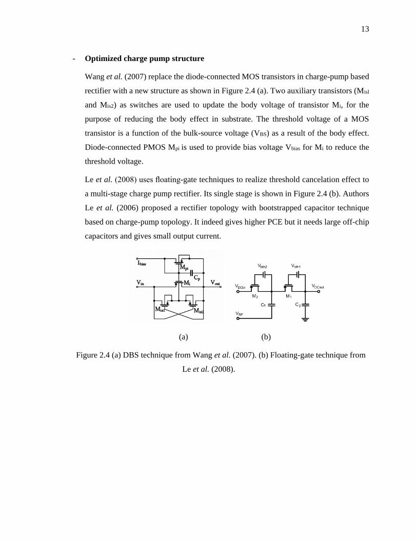
- Optimized charge pump structure
Wang et al. (2007) replace the diode-connected MOS transistors in charge-pump based
rectifier with a new structure as shown in Figure 2.4 (a). Two auxiliary transistors (Misl
and Mis2) as switches are used to update the body voltage of transistor Mi, for the
purpose of reducing the body effect in substrate. The threshold voltage of a MOS
transistor is a function of the bulk-source voltage (VBS) as a result of the body effect.
Diode-connected PMOS Mpi is used to provide bias voltage Vbias for Mi to reduce the
threshold voltage.
Le et al. (2008) uses floating-gate techniques to realize threshold cancelation effect to
a multi-stage charge pump rectifier. Its single stage is shown in Figure 2.4 (b). Authors
Le et al. (2006) proposed a rectifier topology with bootstrapped capacitor technique
based on charge-pump topology. It indeed gives higher PCE but it needs large off-chip
capacitors and gives small output current.
(a) (b)
Figure 2.4 (a) DBS technique from Wang et al. (2007). (b) Floating-gate technique from
Le et al. (2008).

14
CHAPTER 3 RECTIFIER DESIGN AND POST-LAYOUT
SIMULATION
Rectifier is the most important block of a RF-EH system and should be critically designed
because it greatly influences the overall performance of the harvesting system. In this chapter,
popular rectifier structures are studied in the first place. Then the designed 3-stage FGCC rectifier
dedicated for 880MHz GSM band is presented in the second part. The benefits of employing
multiple stages, low-threshold-voltage (LTV) transistors and bulk-GND connection are discussed
at the same time. In addition, the layout design of this rectifier is also presented. The post-layout
simulation results are given at the end of this chapter.
3.1 Overview of rectifiers: popular CMOS rectifier structures
Diode is the main component in a rectifier, which allows one-way flow of the electrons. In
CMOS technology, a PN junction is usually used as a diode for designers. However, it has a typical
threshold voltage of 0.7 V, which is apparently too high for the input signal to exceed in our
application. In other words, it is not suitable for rectifying low level signals. As we know, schottky
diode has very low threshold voltage, low conduction resistance, low junction capacitance and also
very large saturation current. However, since conventional CMOS integrated circuits generally do
not employ Schottky junction diodes, Schottky diodes are not known to be available in all standard
CMOS semiconductor fabrication processes (Ma et al. (2014)). Schottky junction diodes of the
prior art require specialized semiconductor fabrication processes, which raises the cost of chip
fabrication because extra masks need to be produced by the Fabs which use modular process
(Shokrani et al. (2014)). Besides, although the foundries have already began to adopt Schottky
diodes into modular process in recent years, accurate model of the schottky diode for simulation
are not well prepared and matured enough (Yuan et al. (2015)). Thus schottky diodes in rectifier
design are replaced by diode-connected CMOS transistors. However, the voltage needed for
turning on the transistor diode is higher than that of a schottky diode. Therefore, transistors working
as switches are adopted in some rectifier structures. In this section, different popular CMOS
rectifier structures are analyzed. All the recently published advanced rectifiers are derived or
improved from these basic and conventional CMOS rectifier structures.

15
3.1.1 Basic structures of MOS-based rectifier
A: Half-wave structure
The MOS-based half-wave rectifier circuit normally utilizes a single diode-connected MOS
transistor, as shown in Figure 3.1. When it is placed in series with the load capacitor across an AC
supply, it converts alternating voltage into uni-directional pulsating voltage. It uses half cycles of
the applied voltage, either the positive or negative half of the AC wave, and the other half cycle is
suppressed because the diode-connected MOS transistor conducts only in one direction.
An analysis of one-stage conventional MOS-based half-wave rectifier was presented in Yi
et al. (2007) based on the BSIM3 transistor model with appropriate approximations. Figure 3.2
gives the steady-state waveforms of a half wave rectifier. Between t1 and t2, the diode-connected
transistor begins to conduct in sub-threshold region. At t=t2, the input voltage rises higher than the
output voltage by VTH (threshold voltage of the diode-connected transistor). At this moment, the
transistor gets into saturation region. Between t2 and t3, the transistor keeps working in saturation
region, and the drain-to-source current of the transistor id(t) equals to2( )gs THV V . This state
continues until the input voltage drops to just higher than the output voltage by VTH at t=t4. Between
t3 and t4, the transistor works in sub-threshold region again. Between t4 and t1+T (T is the period of
the input AC voltage signal), the drain and source of the transistor are interchanged. The transistor
works in sub-threshold region with 0gsV and ( ) ( )ds out inV V t V t . During this time period, the
current id(t) is considered as leakage current Ileak. In the micro-power regime, Ileak cannot be
neglected. This is because:
(1) Ileak increases exponentially with the decrease in VTH, and, for low-VTH and zero-VTH
devices, Ileak can be of the order of μA and is thus not negligibly small;
(2) Ileak is comparable to the load current in micro-power rectifiers;
(3) the power consumed by Ileak is significant as the transistor stays in the reverse-biased
region for a considerable period of time. (Yi et al. (2007))
Half-wave topology is simple and easy to be understood. However, it is not efficient
because it uses only the half of the input signal cycle. For low-power-consumption electronic
devices, half-wave topology is not the best choice.

16
Figure 3.1 Conventional MOS-based half-wave rectifier
Figure 3.2 Waveforms of the conventional MOS-based half-wave rectifier from Yi et al. (2007):
(a) Waveforms of input and output voltages, (b) Waveforms of transistor current.
B: Full-wave bridge structure
The full-wave rectifier is a little more complicated than the half-wave one. It utilizes both
halves of the input AC waveform to provide an output. This greatly improves the efficiency and
leads the output to be much easier to be smoothed. The full-wave bridge nMOS-based topology is
presented in Figure 3.3.
Taking this circuit as an example, during the positive half cycle of the supply, diodes N3
and N2 conduct in series while diodes N4 and N1 are reverse biased and the current flows through
17
the load from top to bottom. During the negative half cycle of the supply, diodes N4 and N1 conduct
in series, but diodes N3 and N2 switch "OFF" as they are now reversed biased. The current flowing
through the load has the same direction as that of the positive half circuit. As the current flowing
through the load is unidirectional, the voltage developed across the load is also unidirectional.
The bulk of the nMOS transistors in Figure 3.3 are connected to the rectifier output. This
bulk biasing method leads to latch-up hazard, and leakage current Ileak during “OFF” state, same as
what we discussed earlier in the half-wave topology section. To overcome the disadvantages,
Onizuka et al. (2006) use DBS technique to reduce the undesirable body effect of the main diode-
connected PMOS transistor, as presented in Figure 2.1.
The efficiency of full-wave rectifier is higher than the half-wave one, but it is still limited
by the voltage drop of two diodes in each single cycle, especially in low-voltage applications.
Figure 3.3 Conventional MOS-based full-wave bridge rectifier (nMOS transistors are used)
3.1.2 Advanced bridge MOS-based rectifiers
As we saw in the previous section, conventional full-wave bridge rectifier uses two pairs of
diode-connected MOS transistors. The effective turn-on voltage of the diode-connected MOS
transistor is almost equal to the threshold voltage of the MOS transistor, which is smaller than a
PN-junction diode, but generally larger than a Schottky diode. Since a pair of diodes turns on at
each cycle in series with the input RF signal, the output voltage is twice as low as the threshold
voltage of the MOS transistor below the amplitude of the input RF signal. Therefore, in such
structure, high PCE cannot be achieved. In order to get high PCE, several advanced rectifier
topologies have been proposed.
vin+
vin-
Cload Rload
N1
N2
N3
N4
Vout

18
A: Partially Gate Cross-Coupled structure (PGCC)
In partially gate cross-coupled structure, two diode-connected transistors in conventional
full-wave bridge structure are replaced by two cross-coupled transistors (N1 and N2) as shown in
Figure 3.4. During the positive half cycle, only diode N3 and switch N2 turn on. The current goes
out of node Vout from terminal Vin+ through diode N3 and flows through the load Rload. Then the
current goes back to terminal Vin- from the load through switch N2. Ground acts as a reference
voltage. During the negative half cycle, diode N4 and switch N1 turn on. At this time, the current
goes out of node Vout from terminal Vin- through N4 and flows through the load. Then the current
goes back to terminal Vin+ from the load through N1. In each case, the negative terminal of the
source is connected to the ground and the positive terminal transfer the positive voltage to the
output. A DC voltage is generated across the load resistor.
The advantage of this topology comparing with the conventional diode-connected full-wave
topology is that the voltage drop across the switch transistors can be lower than threshold voltage
if they are properly sized. Thus DBS technique is adopted in some works as we introduced and
presented in section 2.4. However, the switch transistors lead to substrate leakage and possible
latch-up.
Figure 3.4 Partially gate cross-coupled rectifier (nMOS transistors are used)
B: Fully Gate Cross-Coupled structure (FGCC)
As shown in Figure 3.5, this circuit has a cross-coupled differential CMOS configuration
with a bridge structure. In this rectifier, all the four transistors are used as switches.
vin+
vin-
Cload Rload
N1
N2
N3
N4
Vout

19
When Vin+ is high and Vin- is low (during the positive half of the switching cycle),
transistor P1 and N2 are on and P2 and N1 are off, assuming that Vin+ and Vin- are large enough to
turn the transistors on and off. Current flows out of Vout through P1 and flows into negative
terminal of the source through N2. During the other half of the cycle, P1 and N2 are off and P2 and
N1 are on. In this case, current flows out of Vout through P2 and flows into positive terminal of the
source through N1. Therefore, a DC voltage is generated across the load resistance.
In this circuit, the on-resistance of the transistors is decreased by increasing gate-source
voltage (|VGS|) of the transistors and the reverse leakage is reduced by reversing the polarity of the
VGS in the cross-coupled structures. Thus, the PCE of this circuit is higher than those of the previous
rectifier circuits.
Figure 3.5 Fully gate cross-coupled rectifier
C: Charge-Pump Based Rectifiers
The charge-pump based rectifier is mostly based on the Dickson's topology. In this topology
as shown in Figure 3.6 (nMOS and pMOS complementary version), diode-connected transistors
are used as pumping devices. During the negative half cycle, MP2 turns off and MN1 turns on
resulting in capacitor C being charged to |Vin|. When Vin goes into the positive half cycle, MN1
turns off and MP2 turns on. In this case the charges stored in capacitor C flows into load capacitor
CL through MP2, thus the top plate of capacitor C (its right side in Figure 3.6) is pushed up to 2|Vin|
and this voltage appears at the output.
Ideally the output voltage should be 2|Vin|, but in fact the output voltage is reduced by the
threshold of the rectifying transistors. The output voltage of a single stage charge-pump based
rectifier can be expressed as (Dickson (1976)):
vin+
vin-
Cload Rload
N1
N2
P1
P2
Vout
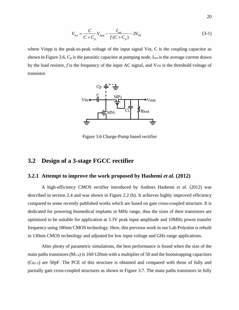
20
2( )
outout inpp TH
p p
ICV V V
C C f C C
(3-1)
where Vinpp is the peak-to-peak voltage of the input signal Vin, C is the coupling capacitor as
shown in Figure 3.6, Cp is the parasitic capacitor at pumping node, Iout is the average current drawn
by the load resistor, f is the frequency of the input AC signal, and VTH is the threshold voltage of
transistor.
Figure 3.6 Charge-Pump based rectifier
3.2 Design of a 3-stage FGCC rectifier
3.2.1 Attempt to improve the work proposed by Hashemi et al. (2012)
A high-efficiency CMOS rectifier introduced by Authors Hashemi et al. (2012) was
described in section 2.4 and was shown in Figure 2.2 (b). It achieves highly improved efficiency
compared to some recently published works which are based on gate cross-coupled structure. It is
dedicated for powering biomedical implants in MHz range, thus the sizes of their transistors are
optimized to be suitable for application at 3.3V peak input amplitude and 10MHz power transfer
frequency using 180nm CMOS technology. Here, this previous work in our Lab Polystim is rebuilt
in 130nm CMOS technology and adjusted for low input voltage and GHz range applications.
After plenty of parametric simulations, the best performance is found when the size of the
main paths transistors (M1-4) is 160/120nm with a multiplier of 50 and the bootstrapping capacitors
(CB1-2) are 50pF. The PCE of this structure is obtained and compared with those of fully and
partially gate cross-coupled structures as shown in Figure 3.7. The main paths transistors in fully
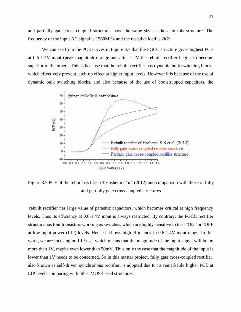
21
and partially gate cross-coupled structures have the same size as those in this structure. The
frequency of the input AC signal is 1960MHz and the resistive load is 2kΩ.
We can see from the PCE curves in Figure 3.7 that the FGCC structure gives highest PCE
at 0.6-1.4V input (peak magnitude) range and after 1.4V the rebuilt rectifier begins to become
superior to the others. This is because that the rebuilt rectifier has dynamic bulk switching blocks
which effectively prevent latch-up effect at higher input levels. However it is because of the use of
dynamic bulk switching blocks, and also because of the use of bootstrapped capacitors, the
rebuilt rectifier has large value of parasitic capacitors, which becomes critical at high frequency
levels. Thus its efficiency at 0.6-1.4V input is always restricted. By contrary, the FGCC rectifier
structure has four transistors working as switches, which are highly sensitive to turn “ON” or “OFF”
at low input power (LIP) levels. Hence it shows high efficiency in 0.6-1.4V input range. In this
work, we are focusing on LIP use, which means that the magnitude of the input signal will be no
more than 1V, maybe even lower than 50mV. Thus only the case that the magnitude of the input is
lower than 1V needs to be concerned. So in this master project, fully gate cross-coupled rectifier,
also known as self-driven synchronous rectifier, is adopted due to its remarkable higher PCE at
LIP levels comparing with other MOS-based structures.
Figure 3.7 PCE of the rebuilt rectifier of Hashemi et al. (2012) and comparison with those of fully
and partially gate cross-coupled structures

22
3.2.2 Analysis of single-stage FGCC rectifier
As shown in Figure 3.8, a single-stage FGCC rectifier consists of two NMOS (N1, N2) and
two PMOS (P1, P2) transistors. A differential input AC signal is fed to this circuit. In order to
better illustrate its operation, the differential input signals (vin+, vin-) and currents through P1 and
N2 (iP1, iN2), which are derived from simulation results, are given in Figure 3.9.
The operation of this circuit can be summarized as follows. During the positive half cycle
of the input AC signal, for example at point A in Figure 3.9, transistors P1 and N2 are “ON” and
P2 and N1 are “OFF”. Current flows out of “Vout” to the load through P1 from the positive terminal
of the input source and flows back to the negative terminal of the input source through N2, as
indicated in Figure 3.8 (a). By doing this, a DC voltage is generated across the load. Here P1 and
N2 work in linear region as two switches. Currents through P1 or N2 can be expressed as:
Figure 3.8 Operation of P1 and N2 of single-stage FGCC CMOS rectifier: (a) Conduction on
linear mode (point A in Figure 3.9), (b) Conduction on subthreshold mode (point B in Figure
3.9).
vin+
vin-
Cload Rload
N1
N2
P1
P2
iP1
iN2
iN2-rev
iP1-rev
Vout
G
D
GS
D
ON
ON
OFF
OFF
OFF
OFFS
vin+
vin-
Cload Rload
N1
N2
P1
P2
Vout
G
D
GS
DON
ONS
Po
siti
ve
cycle
negat
ive
cycl
e
(a)
(b)
_ 1/ 2 21/ 21/ 2 0_ 1/ 2 _ 1/ 2 _ 1/ 2 _ 1/ 2
1/ 2
[( ) ( ) ]2
DS P NP NP N P N ox GS P N TH P N DS P N
P N
vWi C v V v
L (3-2)

23
where iP1/N2 is the drain-to-source current of transistor P1 or N2 (Ampere); μ0-P1/N2 is the electron
mobility of n- or p-type transistor (cm2·V-1·s-1); Cox is the gate-oxide capacitor per unit area (F/cm2);
WP1/N2 and LP1/N2 are effective channel length and width of P1/N2 respectively (μm); VTH-P1/N2 is
the threshold voltage of P1/N2 (V); vGS-P1/N2 and vDS-P1/N2 are gate-to-source and drain-to-source
voltage of P1/N2 respectively. Transistors P2 and N1 work in the same way during the negative
half cycle since this circuit has a symmetrical structure. Therefore, we only discuss transistor P1
and N2 here.
We may easily draw one conclusion from Eq.(3-2) that lower threshold voltage will give
larger iP1/N2. In other words, lower threshold voltage will make the transistors transfer the current
to the load more easily during their “ON” mode, which may lead to a higher PCE. The on resistance
of transistor P1 or N2 (rON-P1/N2) can be derived from Eq.(3-2):
We may draw the second conclusion from Eq.(3-3): larger width/length ratio may decrease
the on resistance, meaning that the voltage drop across the conducting transistor will decrease,
which may improve the PCE. PCE is defined by:
Figure 3.9 Theoretical analysis of single-stage FGCC rectifier
Vo
ltag
e (m
V)
Curr
ent
(uA
)
0.0
iN2
iP1
250.0
500.0
750.0
1000.0
0.0
2.5
5.0
7.5
10.0
12.5
-2.5-25024.6265 24.627 24.6275 24.628 24.6285
Time (us)
B
A A A
B
vin-vin+
1/ 2
1/ 2_ 1/ 2
1/ 2 0_ 1/ 2 _ 1/ 2 _ 1/ 2 _ 1/ 2
_ 1/ 2
1
( ) ( )
( )
P N
P NON P N
P N P N ox GS P N TH P N DS P N
DS P N
L
Wr
i C v V v
v
(3-3)

24
(3-4)
where T is the period of the input AC signal. However, note that we are discussing the transistors
working on “ON” mode and in linear region (for example at point A in Figure 3.9). Later, when
the magnitude of vin+ falls, for example, to point B in Figure 3.9, the advantages of low threshold
and large width/length ratio transform into disadvantages.
In the shadow area in Figure 3.9, vin+ falls to a smaller value which makes [(vGS-N2) - VTH-
N2] 0 and [(vGS-P1) - VTH-P1] 0. Considering from the perspective of a switch, in this case,
transistor P1 and N2 get into “OFF” mode. Ideally, it is supposed to have no current going through
them. However, since P1 and N2 operate in weak inversion region, there is a small subthreshold
current going through them, as illustrated in Figure 3.8 (b). This small current iP1/N2-rev, flowing in
the reversed direction of the previous working mode, can be expressed by:
(3-5)
where k is Boltzmann constant; T is the absolute temperature; q is the electron charge; n is
subthreshold slope factor; ID0 is a parameter related to process. In this situation, both larger
width/length ratio and low threshold voltage provide convenience for this reversed small current
to go through, which reduces the total charge delivered to the load, resulting lower efficiency.
In conclusion, the design of FGCC rectifier should make trade-off between “ON” current
and reversed subthreshold current by carefully selecting the size and threshold voltage of the
transistors.
3.2.3 Necessity of cascading stages of the FGCC rectifier
Since the maximum output DC voltage can be obtained from a single-stage rectifier is
limited, more stages are needed to produce a higher DC voltage across the load resistor. However,
increasing the number of stages causes more leakage because: (a) body bias on nMOS transistors
in later stages increases with the number of stages, which may reduce the “ON” charging current
_ 1/ 21/ 21/ 2_ 0
1/ 2
exp( / )
GS P NP NP N rev D
P N
vWi I
L n kT q
0
0
2 /, ( ) ( )
1( )
out out loadint T
inin in
t
P V RPCE v vin vin
Pv i dt
T

25
through these nMOS transistors, thus pulls down the PCE, and (b) the total number of transistors
also increases which apparently augments the total reversed subthreshold current (may vary from
several nW to tens of nW depending on the input power, Yi et al. (2007)), thus PCE decreases.
In this work, we expect to have an output to be around 1V to 1.2V at the output. However,
the available magnitude of the input signal in front of the rectifier depends not only on the antenna
but also on the matching network. If we assume a 350mV magnitude of the input signal can be
obtained, after plenty of simulation, three is selected as the number of stages since 3-stage rectifier
gives enough output DC voltage and at the same time it does not lead to too much power loss, as
shown in Figure 3.10. Another reason for choosing number 3 is that, according to some published
works, single-stage and 3-stage FGCC rectifiers are reported to have a peak efficiency higher than
60%. The efficiency cannot be remained this high when the number of stages exceeds five due to
the leakage. For example, the 5-stage FGCC rectifiers developed by Le and Luong (2010) and
Ouda et al. (2013) have efficiency only around 25% when input power is below 0dBm.
The main role of the four capacitors C1-4 is to prevent the generated DC signals at the
outputs of each rectifier stage from flowing back to the input. There is no capacitors at the first
stage, since the output voltage at the output of the first stage is lower than the magnitude of the
input signal. Thus there is no need to prevent the reverse flowing. This explains why for some
designed single-stage FGCC rectifier, no capacitor is used in the input path. In addition, the sizes
of the transistors do not need to be the same in each stage. Simulation results show that adjusting
pMOS transistors to be slightly larger than nMOS transistors and making the transistors in first
stage larger than the others help to improve the efficiency.
Figure 3.10 Proposed three-stage FGCC rectifier
vin+
vin-
Cload Rload
N1
N2
N3
N4
N5
N6
P1
P2
P3
P4
P5
P6
Vout
C1 C3
C2 C4
26
3.2.4 PCE comparison of 3-stage FGCC rectifiers using various transistors
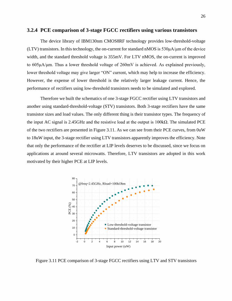
The device library of IBM130nm CMOS8RF technology provides low-threshold-voltage
(LTV) transistors. In this technology, the on-current for standard nMOS is 530μA/μm of the device
width, and the standard threshold voltage is 355mV. For LTV nMOS, the on-current is improved
to 605μA/μm. Thus a lower threshold voltage of 260mV is achieved. As explained previously,
lower threshold voltage may give larger “ON” current, which may help to increase the efficiency.
However, the expense of lower threshold is the relatively larger leakage current. Hence, the
performance of rectifiers using low-threshold transistors needs to be simulated and explored.
Therefore we built the schematics of one 3-stage FGCC rectifier using LTV transistors and
another using standard-threshold-voltage (STV) transistors. Both 3-stage rectifiers have the same
transistor sizes and load values. The only different thing is their transistor types. The frequency of
the input AC signal is 2.45GHz and the resistive load at the output is 100kΩ. The simulated PCE
of the two rectifiers are presented in Figure 3.11. As we can see from their PCE curves, from 0uW
to 18uW input, the 3-stage rectifier using LTV transistors apparently improves the efficiency. Note
that only the performance of the rectifier at LIP levels deserves to be discussed, since we focus on
applications at around several microwatts. Therefore, LTV transistors are adopted in this work
motivated by their higher PCE at LIP levels.
-2 0 2 4 6 8 10 12 14 16 18 20
0
10
20
30
40
50
60
70
80
Standard-threshold-voltage transistor
Low-threshold-voltage transistor
PC
E (
%)
Input power (uW)
@freq=2.45GHz, Rload=100kOhm
Figure 3.11 PCE comparison of 3-stage FGCC rectifiers using LTV and STV transistors
27
3.2.5 PCE comparison of 3-stage FGCC rectifiers using different bulk
connections
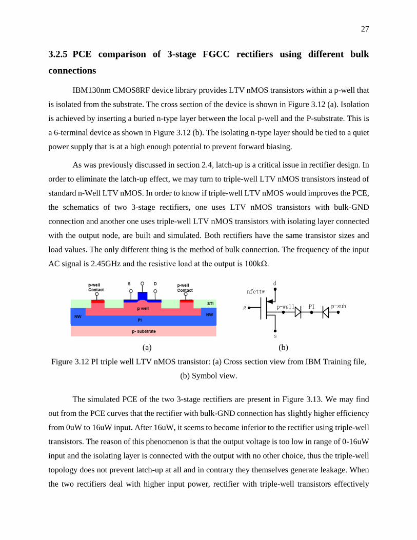
IBM130nm CMOS8RF device library provides LTV nMOS transistors within a p-well that
is isolated from the substrate. The cross section of the device is shown in Figure 3.12 (a). Isolation
is achieved by inserting a buried n-type layer between the local p-well and the P-substrate. This is
a 6-terminal device as shown in Figure 3.12 (b). The isolating n-type layer should be tied to a quiet
power supply that is at a high enough potential to prevent forward biasing.
As was previously discussed in section 2.4, latch-up is a critical issue in rectifier design. In
order to eliminate the latch-up effect, we may turn to triple-well LTV nMOS transistors instead of
standard n-Well LTV nMOS. In order to know if triple-well LTV nMOS would improves the PCE,
the schematics of two 3-stage rectifiers, one uses LTV nMOS transistors with bulk-GND
connection and another one uses triple-well LTV nMOS transistors with isolating layer connected
with the output node, are built and simulated. Both rectifiers have the same transistor sizes and
load values. The only different thing is the method of bulk connection. The frequency of the input
AC signal is 2.45GHz and the resistive load at the output is 100kΩ.
(a) (b)
Figure 3.12 PI triple well LTV nMOS transistor: (a) Cross section view from IBM Training file,
(b) Symbol view.
The simulated PCE of the two 3-stage rectifiers are present in Figure 3.13. We may find
out from the PCE curves that the rectifier with bulk-GND connection has slightly higher efficiency
from 0uW to 16uW input. After 16uW, it seems to become inferior to the rectifier using triple-well
transistors. The reason of this phenomenon is that the output voltage is too low in range of 0-16uW
input and the isolating layer is connected with the output with no other choice, thus the triple-well
topology does not prevent latch-up at all and in contrary they themselves generate leakage. When
the two rectifiers deal with higher input power, rectifier with triple-well transistors effectively
nfettw
g
s
d
p-well PI p-sub

28
prevents latch-up and as a consequence it gives higher efficiency. However, note that the focus of
this project is on LIP use. Therefore, we chose the rectifier using bulk-GND connection.
-2 0 2 4 6 8 10 12 14 16 18 20
0
10
20
30
40
50
60
70
80
PC
E (
%)
Input Power (uW)
@freq=2.45GHz, Rload=100kOhms
Triple-well transistors Bulk-GND connection
Figure 3.13 PCE comparison of 3-stage FGCC rectifier structure using different bulk connection
3.2.6 Design of 3-stage FGCC rectifier
Following the preliminary analysis shown above, we can get to the conclusion that, in order
to design a rectifier intended to operate with several microwatts of input power, and having a higher
efficiency at low power levels, a FGCC structure, composed of three stages in series, and based on
LTV transistors, and bulk-GND connection for nMOS transistors.
Figure in APPENDIX B shows the resulting 3-stage FGCC rectifier built in Virtuoso
Schematic Editor. Power excitation is an 880MHz AC source with zero port resistance. By
carefully selecting the transistor sizes, we obtained good performance.
3.2.7 Layout design
The layout is designed in Virtuoso Layout Suite Editing, using IBM 130nm cmrf8sf
Technology with MA last metal Back End Of Line (BEOL) Metallization Options. The cross
section of this MA last metal Option is presented in APPENDIX A.

29
- Layout of transistors
As shown in Figure 3.14 (a), the gate of nMOS transistor is connected with Metal One
(M1) at both of its two ends, in order to have low resistance gate connection. M1 forms
a gate contact ring. Then a substrate contact ring is designed just outside of the gate
contact ring (p-well tie downs). For the nMOS transistors at the first stage of the rectifier
whose sources and drains are connected with the pads, an N-well guarding is designed
to collect minority electrons injected into the substrate.
As shown in Figure 3.14 (b), the pMOS transistor also has a gate contact ring. And an
N-well contact ring is designed right outside the gate contact ring. This N-well is tied
down by a n+/P-well diode in order to prevent N-well potential from rising too high to
the P-substrate by providing the reverse biased leakage path, as explained in IBM
cmrf8s Design Manual.
(a)
(b)
Figure 3.14 Layout of transistors: (a) nMOS LTV, (b) pMOS LTV.

30
- Layout of capacitors
In this design, dual HP MIM capacitor is employed due to its advantage of area-saving.
Dual HP MIM insert add an additional HY layer to realize parallel connection of two
capacitors. In this way, the capacitance density is increased to 4.10fF/um2.
- Layout of the whole 3-stage FGCC rectifier
The overall area of the designed 3-stage FGCC rectifier including pads is 0,215mm2, as
shown in APPENDIX C.
3.3 Post-layout simulation results of the designed 3-stage FGCC
rectifier
After the layout of the designed 3-stage FGCC rectifier passed Design Rule Check (DRC)
by Calibre DRC and Layout Versus Schematic (LVS) by Calibre LVS, its parasitic capacitors and
resistors are extracted by Assure QRC. Post simulations are run using the extracted file.
3.3.1 Vout simulation
There are different methods to measure power metrics for a circuit using Spectre simulator
and Cadence tools. Since the designed rectifier circuit does not have any power supply, and it is a
non-linear circuit where transistors operate through subthreshold region to linear region, the most
suitable method to know the input power is to measure the input voltage and input current. Then
by applying Eq.(3-6) to the Tool Calculator of Analog Design Environment (ADE), the average
input power P can be plotted.
0
0
1( ) ( )
t T
tP v t i t dt
T
(3-6)
where v(t) is the transient input voltage, i(t) is the transient input current, T is the period of the input
AC signal.
We simulated output voltages of the completed rectifier layout after being extracted, with
50kΩ, 100kΩ and 200kΩ load respectively as shown in Figure 3.15. Being powered by an 880MHz
input AC signal, the designed rectifier can generate 1V at the output at around 15μW (-18.24dBm)
input with 100kΩ load. We find out that the load resistance has

31
impact on the output voltage of the rectifier. When the output is connected with 50kΩ load, 1V
output is generated at around 32μW (-14.95dBm) input power. And if with 200kΩ load, it can
generate 1V at the output at around 7.5μW (-21.25dBm) input. We find that the higher the load
resistance, the lower amount of input power is needed to generate 1V at the output. In other words,
higher load resistance can improves the sensitivity of the rectifier. But it should be noted that
increasing load resistance is not a good method to increase the output voltage, since the load
resistance is always decided and restricted by the circuit block following the rectifier. Hence in this
thesis, the performances of the designed rectifier with different load resistances, 50kΩ, 100kΩ and
200kΩ, are all reported.
3.3.2 PCE simulation
As for the average output power, it can by calculated by:
2( )outout
load
VP
R (3-7)
where Vout is output voltage (V), Rload is the load resistance (Ω).
-2 0 2 4 6 8 10 12 14 16 18 20 22 24 26 28 30
0
200
400
600
800
1000
1200
1400
1600
1800
@880MHz
Outp
ut
Volt
age
(mV
)
Input Power (uW)
200kOhms load
100kOhms load
50kOhms load
Figure 3.15 Vout vs. input power of the designed rectifier with different loads

32
After obtaining both the input and output power, the PCE can be calculated by:
out
in
PPCE
P (3-8)
We simulated the PCE of the designed 3-stage FGCC rectifier with 50kΩ, 100kΩ and
200kΩ load respectively as shown in Figure 3.16. Being fed by an 880MHz input AC signal, the
designed rectifier gives a PCE of 16% at 1μW (-30.0dBm) input and achieves a peak PCE of 70%
at 20μW (-17.0dBm) input with 100kΩ load. The load resistance also has impact on PCE. With
50kΩ load, it gives a PCE of 8.8% at 1μW (-30.0dBm) input and achieves its peak PCE after 30μW
(-15.23dBm) input. And with 200kΩ load, it gives a PCE of 28.5% at 1μW (-30.0dBm) input and
gets to its peak PCE of 67.8% at 8.3μW (-20.81dBm) input. The peak efficiency moves toward
lower input power with the increase of the load resistance, but its value slightly decreases.
Although the proposed rectifier shows great efficiency improvement in LIP range, it still
needs at least 10μW (-20dBm) input power to generate 1.2V at the output. It is not guaranteed that
10μW can be always harvested from single GSM-850MHz band. Thus power combination from
multiple bands is proposed and it will be presented right in next chapter.
-2 0 2 4 6 8 10 12 14 16 18 20 22 24 26 28 30
0
10
20
30
40
50
60
70
80
@ 880MHz
200kOhms load
100kOhms load
50kOhms load
PC
E (
%)
Input Power (uW)
Figure 3.16 PCE vs. input power of the designed rectifier with different loads

33
CHAPTER 4 SYSTEM IMPLEMENTATION AND POST-LAYOUT
SIMULATION
According to the post-simulation results of the designed 3-stage FGCC rectifier at 880MHz
in Chapter 3, in order to obtain a 1V DC voltage across a 200kΩ resistor at the output, at least
7.5μW (-21.25dBm) input power should be available in front of the rectifier. However, as was
previously explained in Chapters 1 and 2, the power density of channel GSM-850 is extremely low,
which means that scavenging 7.5μW (-21.25dBm) RF energy is rather difficult and thus 1V DC
voltage at the output is not guaranteed. Therefore, we attempt to harvest the energy from GSM-
850, GSM-1900 and Wi-Fi 2.4GHz bands at the same time and assemble the energy from these
three channels at the output. In this chapter, a tri-band rectifier system is implemented and
simulated. The topology of the rectifier system is presented in the first place to provide a clear view
for the readers. Furthermore, the post-layout simulation results are reported and discussed. A power
management block to be used for preventing multi-channel reverse leakage is proposed at the end.
4.1 General concept of multi-channel power combination
In Canada, GSM-850, GSM-1900, Wi-Fi 2.4GHz are three largest RF energy contributors.
Generally, GSM-850 uses 824–849 MHz to send information from the mobile station to the base
station (uplink) and 869–894 MHz for the other direction (downlink); GSM-1900 uses 1850–1910
MHz as uplink and 1930–1990 MHz as downlink. Downlink power is always present, and more or
less constant (small power variations during the day), while uplink power depends on the number
of mobile phones in the vicinity of GSM energy harvester (Russo et al. (2013)).Therefore, for
rectifier dedicated for harvesting energy from GSM-850, which is already designed and simulated
in Chapter 3, the center operating frequency of the rectifier is set to be the center frequency of the
GSM-850 downlink band — 880MHz. Similarly, the center operating frequency of rectifier
dedicated for GSM-1900 should be 1960MHz. According to the specifications of IEEE 802.11 for
Wireless Local Area Network (WLAN) computer communication, the center frequency of Wi-Fi
2.4GHz band is 2.45GHz. Therefore, the rectifier dedicated for harvesting energy from Wi-Fi
2.4GHz should have a center operating frequency at 2.45GHz in order to cover the whole band.
For harvesting energy from all these three bands discussed above, another two rectifiers dedicated
for center frequency at 1960MHz and 2.45GHz are designed. The three rectifiers have the same 3-
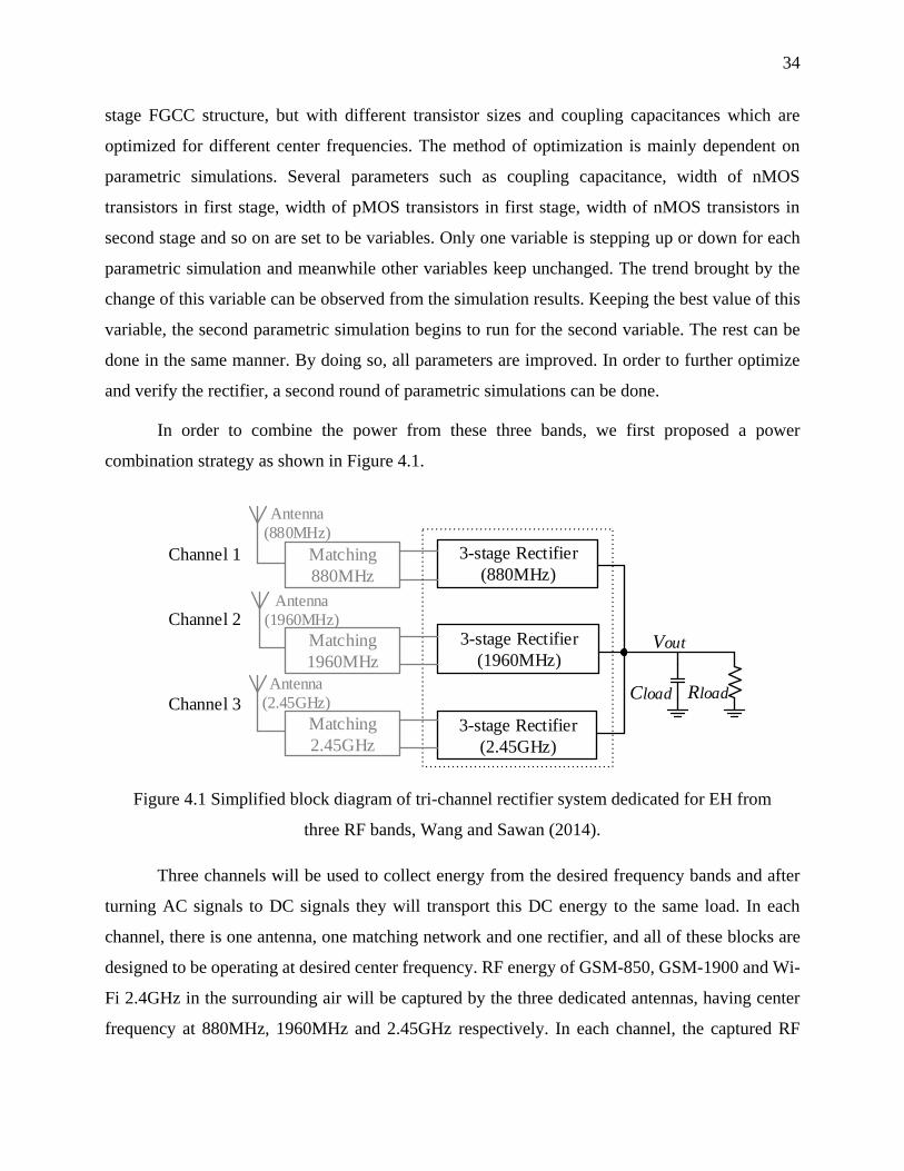
34
stage FGCC structure, but with different transistor sizes and coupling capacitances which are
optimized for different center frequencies. The method of optimization is mainly dependent on
parametric simulations. Several parameters such as coupling capacitance, width of nMOS
transistors in first stage, width of pMOS transistors in first stage, width of nMOS transistors in
second stage and so on are set to be variables. Only one variable is stepping up or down for each
parametric simulation and meanwhile other variables keep unchanged. The trend brought by the
change of this variable can be observed from the simulation results. Keeping the best value of this
variable, the second parametric simulation begins to run for the second variable. The rest can be
done in the same manner. By doing so, all parameters are improved. In order to further optimize
and verify the rectifier, a second round of parametric simulations can be done.
In order to combine the power from these three bands, we first proposed a power
combination strategy as shown in Figure 4.1.
Three channels will be used to collect energy from the desired frequency bands and after
turning AC signals to DC signals they will transport this DC energy to the same load. In each
channel, there is one antenna, one matching network and one rectifier, and all of these blocks are
designed to be operating at desired center frequency. RF energy of GSM-850, GSM-1900 and Wi-
Fi 2.4GHz in the surrounding air will be captured by the three dedicated antennas, having center
frequency at 880MHz, 1960MHz and 2.45GHz respectively. In each channel, the captured RF
Figure 4.1 Simplified block diagram of tri-channel rectifier system dedicated for EH from
three RF bands, Wang and Sawan (2014).
Matching
880MHz
Antenna
(880MHz)
3-stage Rectifier
(880MHz)
Matching
1960MHz
Antenna
(1960MHz)
3-stage Rectifier
(1960MHz)
Matching
2.45GHz
Antenna
(2.45GHz)
3-stage Rectifier
(2.45GHz)
Cload Rload
Vout
Channel 1
Channel 2
Channel 3
35
energy will be fed to the rectifier by the matching circuits. Then the output from each channel will
charge the load capacitor together in the same manner.
This tri-band rectifier system for power combination can be easily realized. However, on
account of the different paces of operation among these rectifiers, we may predict that each rectifier
will be influenced by the other two. The influences could decrease the power efficiency or change
the input impedance. Hence, this power combination topology is being studied and explored
through simulations.
4.2 Post-layout simulation results of multi-channel rectifier
Another two 3-stage FGCC rectifiers dedicated for 1960MHz and 2.45GHz center
frequencies are implemented using the same technology and same transistors/capacitors
arrangements in layout as rectifier for 880MHz.
- PCE simulation
We simulated the PCE of each single-channel rectifier and also those of the tri- and
dual-channel rectifier systems. We define the PCE of multi-channel rectifier system as:
2
, 1 , 2 , 3
/out out load
in in ch in ch in ch
P V RPCE
P P P P
(4-1)
where Pin,ch1/2/3 is the input power to each channel (1, 2 and 3). The method of measuring
Pin,ch1/2/3 is just as we mentioned earlier in chapter 3.
According to our simulation results as presented in Figure 4.2, with 100kΩ load resistor,
the tri-channel rectifier system gives the highest PCE in the range of 0-5μW input power
per channel, improves the PCE by maximum 25% in this input power range, and has a
peak efficiency of 66.3% at 4.9μW input per channel. The dual-channel rectifier system
(880MHz and 1960MHz channels) gives the highest PCE in the range of 5-12μW input
power per channel, improves the PCE by around 20% in this power range, and has a
peak efficiency of around 68% at 8μW input per channel. The three single-channel
rectifiers provide highest PCE after 12μW input power, and have peak efficiencies of
67-70% at around 20μW input power. We find that the peak efficiency moves toward
lower input power levels along with the increase of number of channels.

36
Although the tri-band and dual-band rectifier systems show greatly improved efficiency
at LIP levels, they show non-ideal performance when the input power goes higher than
10μW. Both of them have severe efficiency decrease at HIP levels. The reason for this
phenomenon is that the leakage increases significantly with the increase of number of
channels at HIP levels, which will be discussed in detail in next section.
- Vout Simulation
We simulated the output voltage of each single-channel rectifier and also that of the tri-
channel rectifier system. Although the tri-channel rectifier does not show advantages
on PCE at HIP levels, it has higher sensitivity since its output voltage stays higher than
those of single-channel rectifiers, as shown in Figure 4.3. With 100kΩ load resistor, the
needed input power for single-channel rectifier to generate 1V DC voltage at the output
is 15μW. However, the tri-band rectifier system can generate 1V when the input power
is only 5μW per channel.
-2 0 2 4 6 8 10 12 14 16 18 20 22 24 26 28 30
0
20
40
60
80@ 100kOhms load
PC
E (
%)
Input power per channel (uW)
channel 1 (880MHz)
channel 2 (1960MHz)
channel 3 (2.45GHz)
Dual-channel (880MHz &1960MHz)
Tri-channel (880MHz &1960MHz&2.45GHz)
Figure 4.2 Comparison of PCE of rectifiers with different numbers of channels

37
From Figure 4.2, we know that, when the input power is 5μW per channel, the tri-band
rectifier system still works in its advantageous region. It has an efficiency of 66%. If
we only focus on the circumstance that no more than 5μW can be harvested from each
channel, the tri-band rectifier is definitely superior to the dual-channel rectifier system
and signal-channel rectifiers.
4.3 Reason of the efficiency drop at higher power levels
The reason of the severe efficiency drop, observed from Figure 4.2, for tri- and dual-channel
rectifier systems is explained as follows.
The impedance of the later two channels (1900MHz and 2.4GHz) seen from the output can
be modeled as one resistor Reqi-cha2,3 in parallel with a reactance Xeqi-cha2,3, as shown in Figure 4.4.
The equivalent resistance Reqi-cha2,3 varies with the input power of channels 2 and 3. When the input
power is extremely low, resistance Reqi-cha2,3 has a relatively large value. Thus current mainly flows
through Rload which explains the noticeable improvement in PCE from 0 to 5μW input power.
-4 -2 0 2 4 6 8 10 12 14 16 18 20 22 24 26 28 30
0
200
400
600
800
1000
1200
1400
1600
1800 @ 100kOhms load
Ou
tpu
t v
olt
age
(mV
)
Input power per channel (uW)
Tri-channel (880MHz&1960MHz&2.45GHz)
Single channel (880MHz)
Single channel (1960MHz)
Single channel (2.45GHz)
Figure 4.3 Comparison of Vout of rectifiers with different numbers of channels
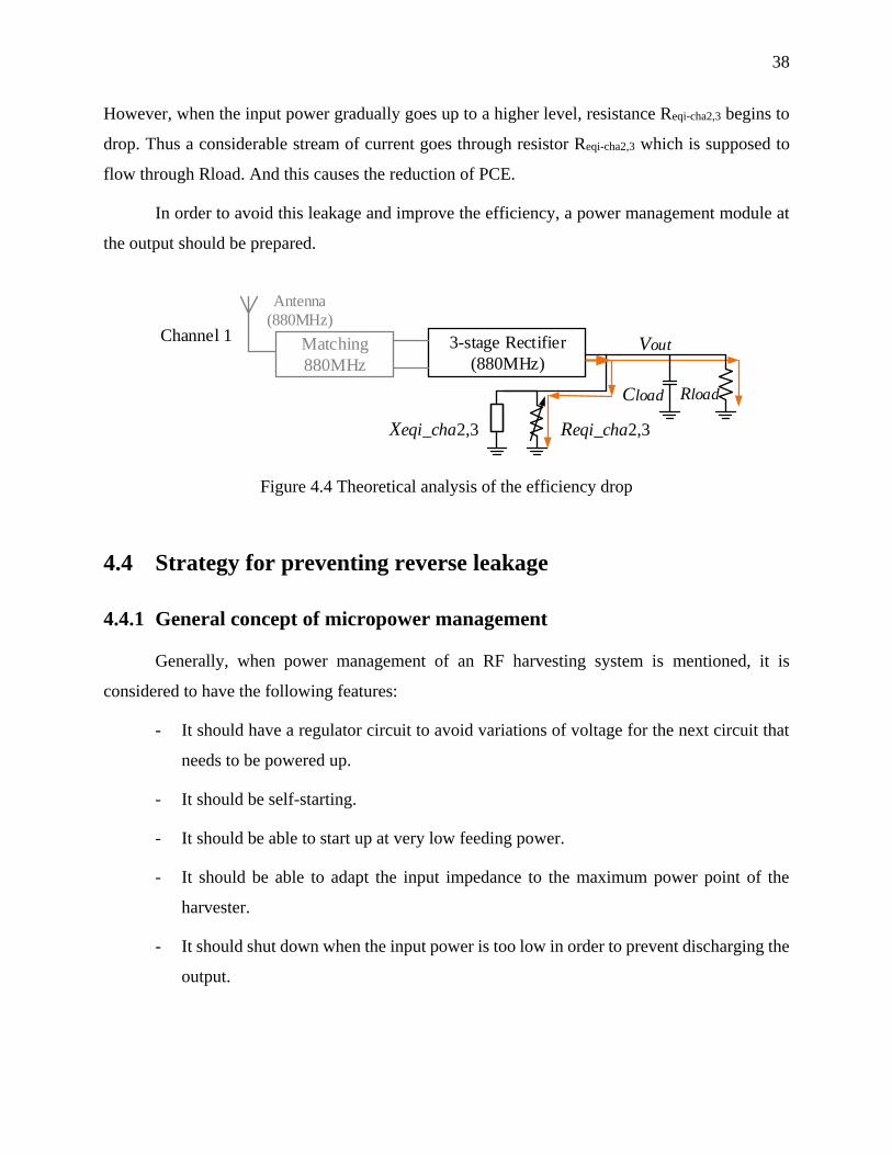
38
However, when the input power gradually goes up to a higher level, resistance Reqi-cha2,3 begins to
drop. Thus a considerable stream of current goes through resistor Reqi-cha2,3 which is supposed to
flow through Rload. And this causes the reduction of PCE.
In order to avoid this leakage and improve the efficiency, a power management module at
the output should be prepared.
4.4 Strategy for preventing reverse leakage
4.4.1 General concept of micropower management
Generally, when power management of an RF harvesting system is mentioned, it is
considered to have the following features:
- It should have a regulator circuit to avoid variations of voltage for the next circuit that
needs to be powered up.
- It should be self-starting.
- It should be able to start up at very low feeding power.
- It should be able to adapt the input impedance to the maximum power point of the
harvester.
- It should shut down when the input power is too low in order to prevent discharging the
output.
Figure 4.4 Theoretical analysis of the efficiency drop
Matching
880MHz
3-stage Rectifier
(880MHz)
Xeqi_cha2,3 Reqi_cha2,3
Antenna
(880MHz)Channel 1
Cload Rload
Vout
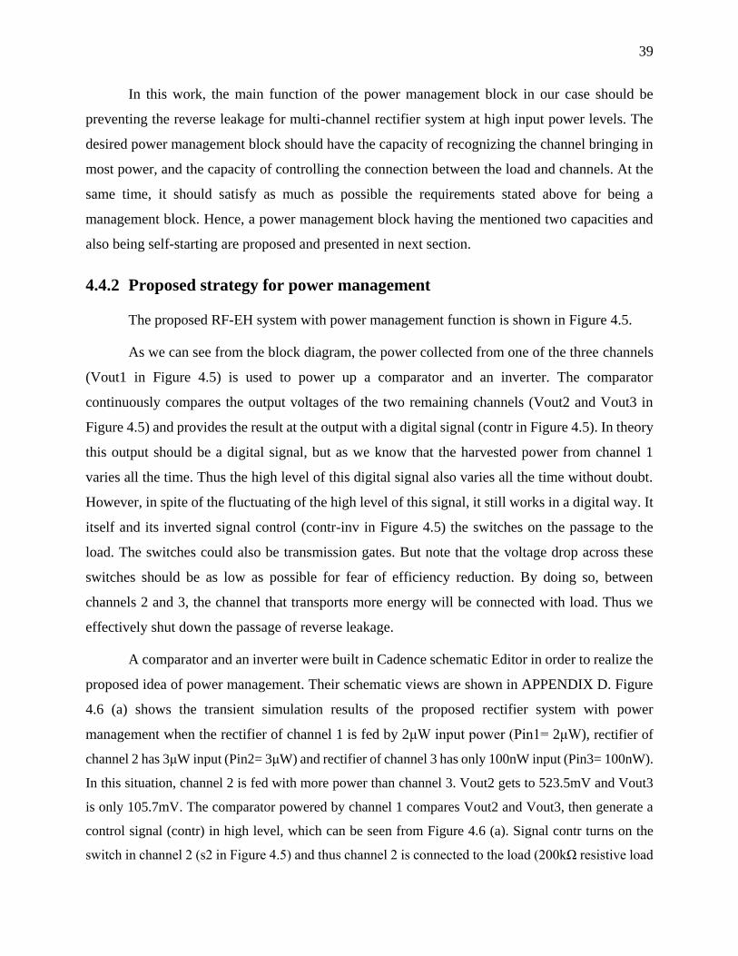
39
In this work, the main function of the power management block in our case should be
preventing the reverse leakage for multi-channel rectifier system at high input power levels. The
desired power management block should have the capacity of recognizing the channel bringing in
most power, and the capacity of controlling the connection between the load and channels. At the
same time, it should satisfy as much as possible the requirements stated above for being a
management block. Hence, a power management block having the mentioned two capacities and
also being self-starting are proposed and presented in next section.
4.4.2 Proposed strategy for power management
The proposed RF-EH system with power management function is shown in Figure 4.5.
As we can see from the block diagram, the power collected from one of the three channels
(Vout1 in Figure 4.5) is used to power up a comparator and an inverter. The comparator
continuously compares the output voltages of the two remaining channels (Vout2 and Vout3 in
Figure 4.5) and provides the result at the output with a digital signal (contr in Figure 4.5). In theory
this output should be a digital signal, but as we know that the harvested power from channel 1
varies all the time. Thus the high level of this digital signal also varies all the time without doubt.
However, in spite of the fluctuating of the high level of this signal, it still works in a digital way. It
itself and its inverted signal control (contr-inv in Figure 4.5) the switches on the passage to the
load. The switches could also be transmission gates. But note that the voltage drop across these
switches should be as low as possible for fear of efficiency reduction. By doing so, between
channels 2 and 3, the channel that transports more energy will be connected with load. Thus we
effectively shut down the passage of reverse leakage.
A comparator and an inverter were built in Cadence schematic Editor in order to realize the
proposed idea of power management. Their schematic views are shown in APPENDIX D. Figure
4.6 (a) shows the transient simulation results of the proposed rectifier system with power
management when the rectifier of channel 1 is fed by 2μW input power (Pin1= 2μW), rectifier of
channel 2 has 3μW input (Pin2= 3μW) and rectifier of channel 3 has only 100nW input (Pin3= 100nW).
In this situation, channel 2 is fed with more power than channel 3. Vout2 gets to 523.5mV and Vout3
is only 105.7mV. The comparator powered by channel 1 compares Vout2 and Vout3, then generate a
control signal (contr) in high level, which can be seen from Figure 4.6 (a). Signal contr turns on the
switch in channel 2 (s2 in Figure 4.5) and thus channel 2 is connected to the load (200kΩ resistive load
40
in this simulation). Observing from Figure 4.6 (a), the curve of Vout is almost overlapped with the
curve of Vout2.
Figure 4.6 (b) shows the transient simulation results of the proposed rectifier system with
power management when Pin2= 100nW and Pin3= 3μW. In this case, being contrary to Figure 4.6
(a), channel 3 is given more energy than channel 2. Vout3 gets to 507.1mV but Vout2 is only
172.1mV. Besides, only 0.4μW power harvested from channel 1 (Pin1= 0.4μW) makes the
comparator and inverter become well functional. As we can see from Figure 4.6 (b), the output
signal of the inverter (contr-inv) is in high level, overlapped with signal Vout1. And this signal
contr-inv successfully turns on the switch in channel 3 (s3 in Figure 4.5), thus connecting channel
3 to the load. The curve of Vout is almost overlapped with that of Vout3, which means that channel
3 is chosen by the comparator since Vout3 is higher than Vout2.
Several transient simulations like these have been conducted and the results of the
simulations preliminarily verify the feasibility of this proposed topology.
Figure 4.5 Proposed RF energy harvesting system with power management
Matching
880MHz
Antenna
(880MHz)
3-stage Rectifier
(880MHz)
Matching
1960MHz
Antenna
(1960MHz)
3-stage Rectifier
(1960MHz)
Matching
2.45GHz
Antenna
(2.45GHz)
3-stage Rectifier
(2.45GHz)Cload Rload
Vout
Channel 1
Channel 2
Channel 3
comparator inverter
Pin1
Pin2
Pin3
Vout1
Vout2
Vout3
contr contr-inv
s2
s3

41
(a)
(b)
Figure 4.6 Transient simulation results of the proposed rectifier system with power management:
(a) when Pin2 >Pin3, (b) when Pin2 <Pin3.

42
CHAPTER 5 MEASUREMENT OF RECTIFIER
The designed rectifier is fabricated with IBM 130nm process. In this chapter, the
measurement setup for testing the fabricated chip is presented in the first place. Then measurement
results of efficiency, output voltage and input impedance are reported.
5.1 Measurement Setup
Measurements were carried out using equipment Agilent (Keysight) PNA-X Network
Analyzer N5247A 10MHz-67GHz, Agilent N1914A EPM Series Power Meter and Oscilloscope.
Due to our analysis in Chapter 3, the FGCC rectifier is a large-signal non-linear circuit. Thus
conventional mixed-mode S-parameter measurements for linear differential circuits using a single-
ended stimulus cannot be used in our case. Although a balun (or hybrid junction) can be used to
feed true differential signal, it is necessary to characterize the hybrid junction itself to obtain its
Touchstone s4p data file before making the measurements which is time-consuming and degrades
measurement accuracy. Thus, in this work, the True-Mode Stimulus Application of PNA is adopted
to apply truly differential input AC signals.
5.1.1 PCB design
In order to guarantee the high-frequency performance of the chip under test and avoid the
influence of parasitic parameters of the chip package, the chip is glued on a substrate Rogers 6002
and the pads on it are directly connected to the copper trace on the substrate by wire bonding. Here,
the main five pads of the rectifier are shown in Figure 5.1. The other pads are test points and are
not presented here since they are dedicated for detailed observation and analysis. The
photomicrograph of the five main pads with wire bonding is shown in Figure 5.2.
The simplified layout view of the PCB is presented in Figure 5.3. The back side of the
substrate is covered by copper as GND. The pads of two inputs (Vin+ and Vin-) are designed to be
connected with two 50Ω SAM Female Jack connectors (leg length 3.8mm) on the left side of Figure
5.3. The two copper transmission lines connecting the inner Pins of connectors and the pads on
chip are designed symmetrically since a truly differential signal will be fed to them. The width of
the two transmission lines is designed to be 25mil, and so does the other lines on the substrate.
Substrate Rogers 6002 has a dielectric constant of 2.94, thus copper transmission lines with a width

43
of 25mil gives a characteristic impedance of 50Ω. By designing like this, the 50Ω lines on substrate
will match with the 50Ω connectors and also match with the 50Ω system of the network analyzer.
The pads of two outputs (Vout+ and Vout-) are designed to be connected with the two horizontal
transmission lines, as shown on the right part of Figure 5.3. A surface-mounted load capacitor and
resistor are connected across the two lines. Two squares of copper are added at the terminals of the
two lines at the edge of substrate for later placing the probe of oscilloscope. The pad of GND_DC
is connected with the transmission line at the upper part of Figure 5.3. This line will be firstly
connected to a DC power supply with zero Volt, and after making sure it works properly, it will be
connected with the GND at the back side.
Figure 5.1 Five main pads shown in schematic view
vin+
vin-
N1
N2
N3
N4
N5
N6
P1
P2
P3
P4
P5
P6
Vout+
Vout-
GND_DC
GND_DC
GND_DC
GND_DC
GND_DC
GND_DC
GND_DC
Figure 5.2 Photomicrograph of fabricated rectifier with its five main pads with wire bonding
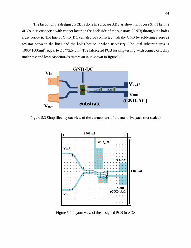
44
The layout of the designed PCB is done in software ADS as shown in Figure 5.4. The line
of Vout- is connected with copper layer on the back side of the substrate (GND) through the holes
right beside it. The line of GND_DC can also be connected with the GND by soldering a zero Ω
resistor between the lines and the holes beside it when necessary. The total substrate area is
1000*1000mil2, equal to 2.54*2.54cm2. The fabricated PCB for chip testing, with connectors, chip
under test and load capacitors/resistors on it, is shown in figure 5.5.
Figure 5.3 Simplified layout view of the connections of the main five pads (not scaled)
Vin+
Vin-
Vout+
Vout -
(GND-AC)
chip RloadCload
Substrate
GND-DC
Figure 5.4 Layout view of the designed PCB in ADS

45
5.1.2 Equipments and calibration
- Power Meter self calibration
Power meter N1914A needs to be self calibration, as shown in Figure 5.6 (a), before it
is used to measure the power from network analyzer.
- Network Analyzer calibration
A: Network Analyzer source calibration
As BAL-BAL (balance to balance) measurement mode of Agilent N5247A Network
Analyzer is used in our case, port 1 and port 3 are set to be the “Balance Port 1”, which
will be fed a truly differential stimulus. In other words, the signals in port 1 and port 3
have the same magnitude and same frequency but 180 degree difference of phase. The
two sources in port 1 and port 3 respectively need to be measured by the power meter
to make sure that they have accurate outputs, as shown in Figure 5.6 (b).
B: Network Analyzer vector calibration
This calibration process employs a technique called vector error correction, in which
error terms are characterized using known standards so that errors can be removed from
actual measurements. For example, the calibration eliminates the impacts of test cables.
The two-port E-cal Agilent 85093-60008 is used as shown in Figure5.6 (c).
Figure 5.5 PCB for chip testing

46
(a) (b)
(c) (d)
Figure 5.6 Calibration: (a) Power meter self calibration, (b) PNA source calibration,
(c) PNA vector calibration, (d) Port extension.
Figure 5.7 Purpose of port extension
Calibration Plane Desired Calibration Plane
Vout+
Vout -
(GND-AC)
chip RloadCload
Substrate
GND-DC
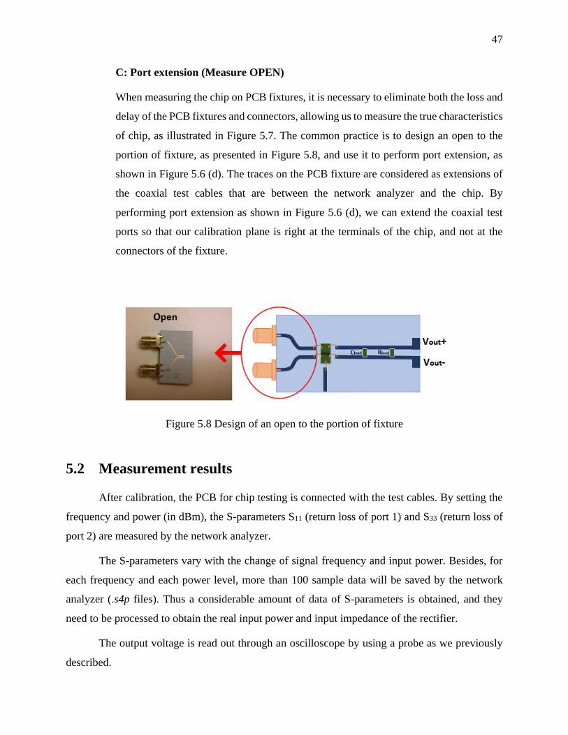
47
C: Port extension (Measure OPEN)
When measuring the chip on PCB fixtures, it is necessary to eliminate both the loss and
delay of the PCB fixtures and connectors, allowing us to measure the true characteristics
of chip, as illustrated in Figure 5.7. The common practice is to design an open to the
portion of fixture, as presented in Figure 5.8, and use it to perform port extension, as
shown in Figure 5.6 (d). The traces on the PCB fixture are considered as extensions of
the coaxial test cables that are between the network analyzer and the chip. By
performing port extension as shown in Figure 5.6 (d), we can extend the coaxial test
ports so that our calibration plane is right at the terminals of the chip, and not at the
connectors of the fixture.
5.2 Measurement results
After calibration, the PCB for chip testing is connected with the test cables. By setting the
frequency and power (in dBm), the S-parameters S11 (return loss of port 1) and S33 (return loss of
port 2) are measured by the network analyzer.
The S-parameters vary with the change of signal frequency and input power. Besides, for
each frequency and each power level, more than 100 sample data will be saved by the network
analyzer (.s4p files). Thus a considerable amount of data of S-parameters is obtained, and they
need to be processed to obtain the real input power and input impedance of the rectifier.
The output voltage is read out through an oscilloscope by using a probe as we previously
described.
Figure 5.8 Design of an open to the portion of fixture

48
5.2.1 Process of data
In order to process the large amount of data with high efficiency and high accuracy, a s4p
block in 50Ω system is modeled in ADS as shown in Figure 5.9. By filling the s4p files from
network analyzer into the model, we can plot the input impedances of the rectifier at different
frequency and different input power by setting equations:
111
11
150
1
SZ
S
(5-1)
333
33
150
1
SZ
S
(5-2)
Ideally, the value of Z1 and Z3 should be the same since the FGCC rectifier structure is
symmetrical. However, due to the different layout routing, they are slightly different at low
frequency and much more different at higher frequency range. The consequence of this will be
discussed in the flowing section. Here the reported input impedance is the average of Z1 and Z3.
5.2.2 Measurement results
- Efficiency measurement
The real input power Pin, the power really fed into the rectifier, is calculated by
Figure 5.9 Model of s4p block in ADS for processing data

49
2 2
11 11(1 )in s dd cdP P S S (5-3)
where Ps is the source power, Sdd11 is the differential-to-differential mode reflection
coefficient, and Scd11 is differential-to-common mode reflection coefficient.
Sdd11 can be directly plotted on the network screen, and it also can be obtained through
the built s4p block in ADS by setting equation:
11 11 31 13 33
1( )
2ddS S S S S (5-4)
So does Scd11:
11 11 31 13 33
1( )
2cdS S S S S (5-5)
Firstly, the PCE curves of the fabricated rectifiers are presented. They are the average
results measured from nine chip samples. Each sample was measured three times.
-30 -25 -20 -15 -10 -5 0 5
-5
0
5
10
15
20
25
30
35
40
45
50
55
60
65
70
Po
wer
co
nv
ersi
on
eff
icie
ncy
(%
)
Input Power (dBm)
100kOhms resistive load
50kOhms resistive load
10kOhms resistive load
@880MHz
Figure 5.10 Measured PCE as a function of input power at 880MHz with 100kΩ, 50kΩ and 10kΩ
load resistor
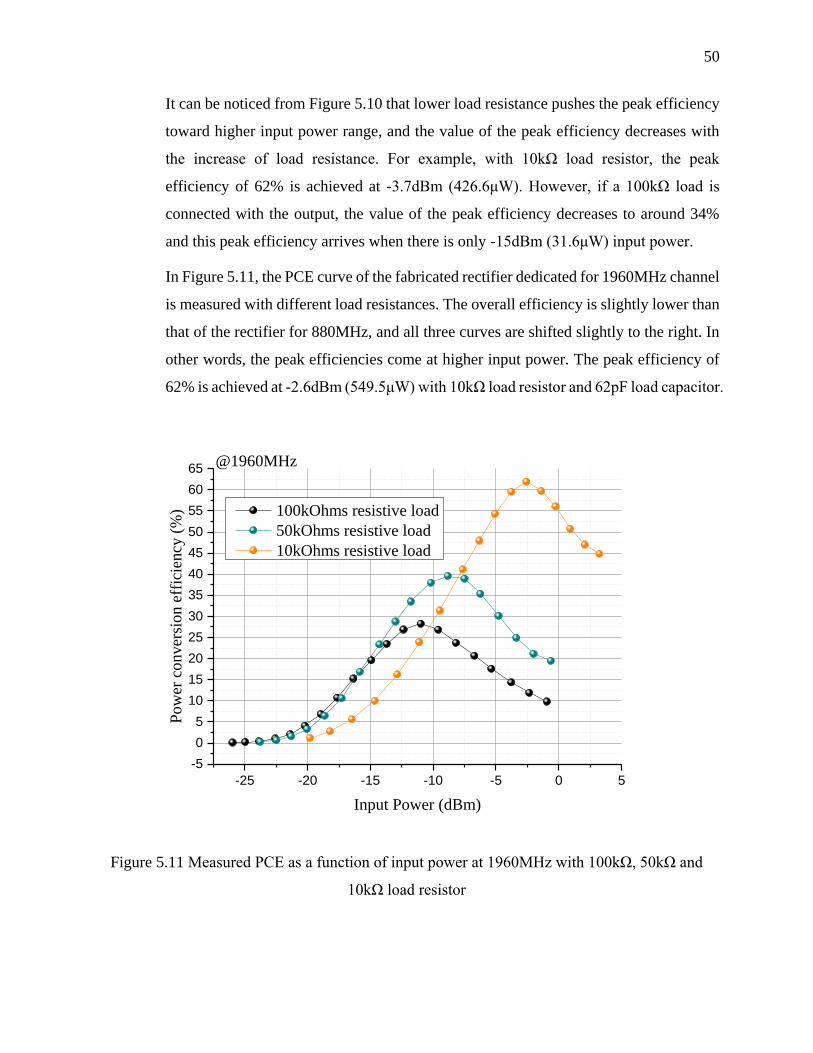
50
It can be noticed from Figure 5.10 that lower load resistance pushes the peak efficiency
toward higher input power range, and the value of the peak efficiency decreases with
the increase of load resistance. For example, with 10kΩ load resistor, the peak
efficiency of 62% is achieved at -3.7dBm (426.6μW). However, if a 100kΩ load is
connected with the output, the value of the peak efficiency decreases to around 34%
and this peak efficiency arrives when there is only -15dBm (31.6μW) input power.
In Figure 5.11, the PCE curve of the fabricated rectifier dedicated for 1960MHz channel
is measured with different load resistances. The overall efficiency is slightly lower than
that of the rectifier for 880MHz, and all three curves are shifted slightly to the right. In
other words, the peak efficiencies come at higher input power. The peak efficiency of
62% is achieved at -2.6dBm (549.5μW) with 10kΩ load resistor and 62pF load capacitor.
-25 -20 -15 -10 -5 0 5
-5
0
5
10
15
20
25
30
35
40
45
50
55
60
65
Po
wer
co
nv
ersi
on
eff
icie
ncy
(%
)
Input Power (dBm)
100kOhms resistive load
50kOhms resistive load
10kOhms resistive load
@1960MHz
Figure 5.11 Measured PCE as a function of input power at 1960MHz with 100kΩ, 50kΩ and
10kΩ load resistor
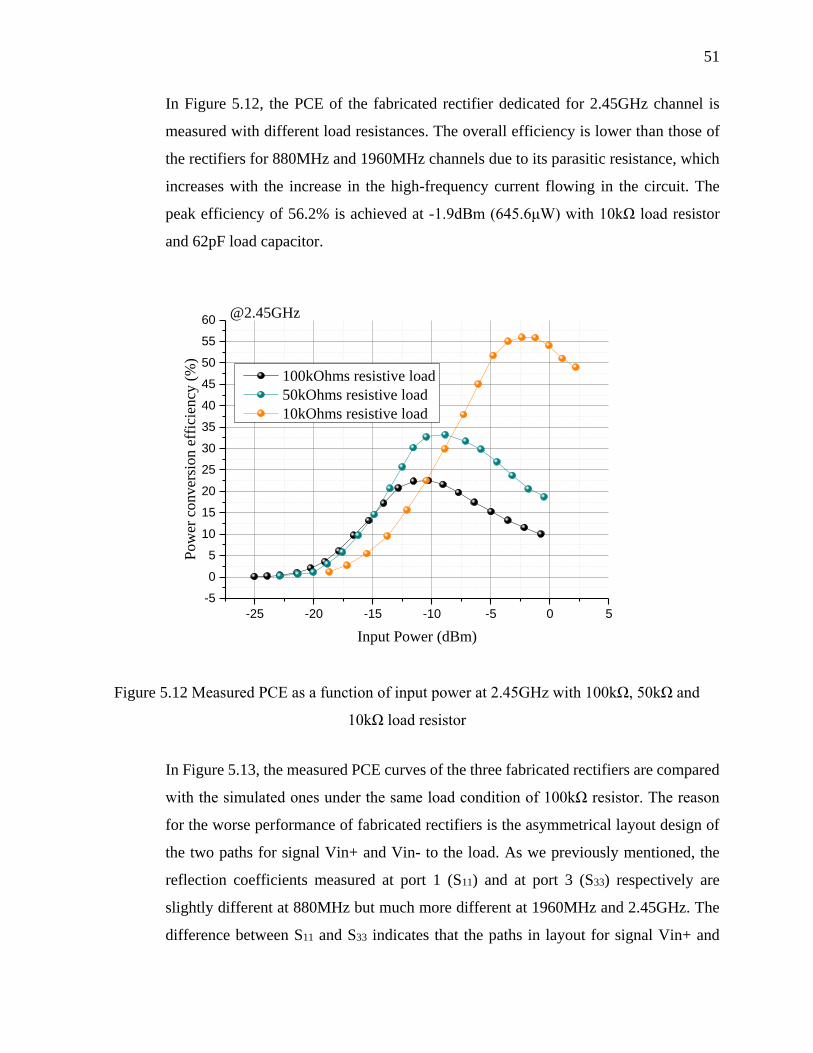
51
In Figure 5.12, the PCE of the fabricated rectifier dedicated for 2.45GHz channel is
measured with different load resistances. The overall efficiency is lower than those of
the rectifiers for 880MHz and 1960MHz channels due to its parasitic resistance, which
increases with the increase in the high-frequency current flowing in the circuit. The
peak efficiency of 56.2% is achieved at -1.9dBm (645.6μW) with 10kΩ load resistor
and 62pF load capacitor.
In Figure 5.13, the measured PCE curves of the three fabricated rectifiers are compared
with the simulated ones under the same load condition of 100kΩ resistor. The reason
for the worse performance of fabricated rectifiers is the asymmetrical layout design of
the two paths for signal Vin+ and Vin- to the load. As we previously mentioned, the
reflection coefficients measured at port 1 (S11) and at port 3 (S33) respectively are
slightly different at 880MHz but much more different at 1960MHz and 2.45GHz. The
difference between S11 and S33 indicates that the paths in layout for signal Vin+ and
-25 -20 -15 -10 -5 0 5
-5
0
5
10
15
20
25
30
35
40
45
50
55
60
Po
wer
co
nv
ersi
on
eff
icie
ncy
(%
)
Input Power (dBm)
100kOhms resistive load
50kOhms resistive load
10kOhms resistive load
@2.45GHz
Figure 5.12 Measured PCE as a function of input power at 2.45GHz with 100kΩ, 50kΩ and
10kΩ load resistor
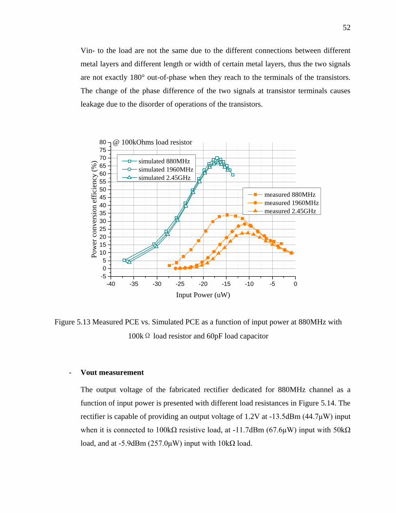
52
Vin- to the load are not the same due to the different connections between different
metal layers and different length or width of certain metal layers, thus the two signals
are not exactly 180° out-of-phase when they reach to the terminals of the transistors.
The change of the phase difference of the two signals at transistor terminals causes
leakage due to the disorder of operations of the transistors.
- Vout measurement
The output voltage of the fabricated rectifier dedicated for 880MHz channel as a
function of input power is presented with different load resistances in Figure 5.14. The
rectifier is capable of providing an output voltage of 1.2V at -13.5dBm (44.7μW) input
when it is connected to 100kΩ resistive load, at -11.7dBm (67.6μW) input with 50kΩ
load, and at -5.9dBm (257.0μW) input with 10kΩ load.
-40 -35 -30 -25 -20 -15 -10 -5 0
-5
0
5
10
15
20
25
30
35
40
45
50
55
60
65
70
75
80
simulated 880MHz
simulated 1960MHz
simulated 2.45GHz
Pow
er c
onver
sion e
ffic
iency
(%
)
Input Power (uW)
measured 880MHz
measured 1960MHz
measured 2.45GHz
@ 100kOhms load resistor
Figure 5.13 Measured PCE vs. Simulated PCE as a function of input power at 880MHz with
100kΩ load resistor and 60pF load capacitor
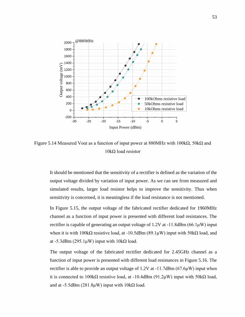
53
It should be mentioned that the sensitivity of a rectifier is defined as the variation of the
output voltage divided by variation of input power. As we can see from measured and
simulated results, larger load resistor helps to improve the sensitivity. Thus when
sensitivity is concerned, it is meaningless if the load resistance is not mentioned.
In Figure 5.15, the output voltage of the fabricated rectifier dedicated for 1960MHz
channel as a function of input power is presented with different load resistances. The
rectifier is capable of generating an output voltage of 1.2V at -11.8dBm (66.1μW) input
when it is with 100kΩ resistive load, at -10.5dBm (89.1μW) input with 50kΩ load, and
at -5.3dBm (295.1μW) input with 10kΩ load.
The output voltage of the fabricated rectifier dedicated for 2.45GHz channel as a
function of input power is presented with different load resistances in Figure 5.16. The
rectifier is able to provide an output voltage of 1.2V at -11.7dBm (67.6μW) input when
it is connected to 100kΩ resistive load, at -10.4dBm (91.2μW) input with 50kΩ load,
and at -5.5dBm (281.8μW) input with 10kΩ load.
-30 -25 -20 -15 -10 -5 0 5
-200
0
200
400
600
800
1000
1200
1400
1600
1800
2000
Outp
ut
volt
age
(mV
)
Input Power (dBm)
100kOhms resistive load
50kOhms resistive load
10kOhms resistive load
@880MHz
Figure 5.14 Measured Vout as a function of input power at 880MHz with 100kΩ, 50kΩ and
10kΩ load resistor

54
-25 -20 -15 -10 -5 0 5
-200
0
200
400
600
800
1000
1200
1400
1600
1800
2000
Outp
ut
volt
age
(mV
)
Input Power (dBm)
100kOhms resistive load
50kOhms resistive load
10kOhms resistive load
@1960MHz
Figure 5.15 Measured Vout as a function of input power at 1960MHz with 50kΩ, 100kΩ and
200kΩ load resistor
-25 -20 -15 -10 -5 0 5
-200
0
200
400
600
800
1000
1200
1400
1600
1800
2000
Ou
tpu
t v
olt
age
(mV
)
Input Power (dBm)
100kOhms resistive load
50kOhms resistive load
10kOhms resistive load
@2.45GHz
Figure 5.16 Measured Vout as a function of input power at 2.45GHz with 50kΩ, 100kΩ and
200kΩ load resistor

55
- Input impedance measurement
The output waveform of a rectifier commonly has ripples due to the charging and
discharging procedures of the load capacitor. It is often desirable for designers to reduce
the amount of output ripples. The magnitude of the rectifier output ripples can be
reduced by increasing the source operating frequency, or by using larger load
capacitances. In this work, a 62pF load capacitor is employed. Thus the following
reported input impedances of the rectifiers include this 62pF load capacitor and 100kΩ
load resistor.
Setting up in a 50Ω system, the measured real part of Zin as a function of input power
at 880MHz, 1960MHz and 2.45GHz respectively is presented in Figure 5.17. The real
part of Zin (rectifiers for channel 880MHz and 1960MHz) increases with the increase
in input power.
-30 -25 -20 -15 -10 -5 0 5
10
20
30
40
50
60
70
80
90
100
Rea
l (Z
in)
(Ohm
)
Input power (dBm)
2.45GHz
1960MHz
880MHz
@100kOhms RLOAD, 62pF CLOAD
Figure 5.17 Measured real part of Zin as a function of input power of the rectifiers dedicated for
880MHz, 1960MHz and 2.45GHz respectively
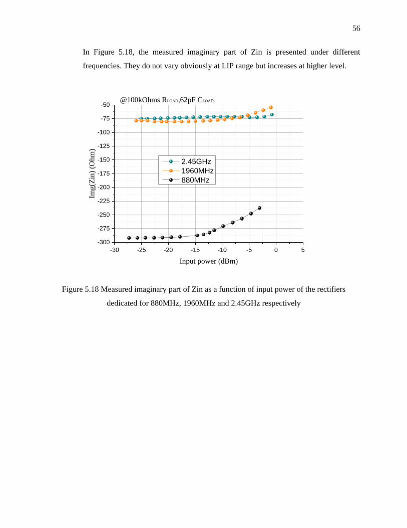
56
In Figure 5.18, the measured imaginary part of Zin is presented under different
frequencies. They do not vary obviously at LIP range but increases at higher level.
-30 -25 -20 -15 -10 -5 0 5
-300
-275
-250
-225
-200
-175
-150
-125
-100
-75
-50
Img
(Zin
) (O
hm
)
Input power (dBm)
2.45GHz
1960MHz
880MHz
@100kOhms RLOAD,62pF CLOAD
Figure 5.18 Measured imaginary part of Zin as a function of input power of the rectifiers
dedicated for 880MHz, 1960MHz and 2.45GHz respectively

57
CHAPTER 6 TRI-BAND ANTENNA DESIGN
The designed rectifier block of RF-EH system was discussed in chapter 3-5. In this chapter,
design of the antenna block is presented. Firstly, basic concept of RF power transmission is
introduced. The vital functions of antenna design are also explained. In the second part, general
characteristics and advantages of microstrip patch antenna (MPA) are introduced. Then a new low-
volume RF harvesting system is presented. This new system uses a tri-band antenna instead of
three discrete single-band antennas. The geometry of the designed tri-band MPA antenna with its
simulation results are presented and reported.
6.1 RF power transmission
The function of the antenna in an RF-EH system is to receive instead of to radiate. It
captures energy from an incoming electromagnetic field and converts the electromagnetic waves
into electric current.
The concept of RF power transmission is shown in Figure 6.1. For our case, the base station
works as the source and the power transmitted by it will be received by the harvesting devices.
Friis equation:
2
4r t t rP PG G
r
(6-1)
one of the most important equations in antenna design, gives an estimate of received power from
the source, where Pr and Pt are the received power and transmitted power in Watts at the antenna
terminals, respectively. Gr and Gt are the antenna gain at receiving and transmitting. λ is the
wavelength of the signal and r is the distance between the transmit and receive antennas. This
equation reveals that, in order to receive large amounts of energy (Pr) at the devices, either the
harvesting devices stay near to the source (r) or they have a high-gain antenna (Gr), in the case of
fixed signal frequency (f), fixed Gt and fixed Pt.
The received power Pt can also be expressed as:
t eP S A (6-2)
where S is the power density at the receive antenna and Ae is the effective area of the receive
antenna.

58
The amplitude of the voltage generated on the antenna va depends on the receiving power
Pr and the antenna radiation resistance Rr:
2 2a r rv R P
(6-3)
According to Eq.(6-3), we may deduce that va will be very low and will be on the order of tens of
millivolts. For example, a typical half wave dipole operating in free space has a radiation resistance
of around 73 Ω and the received power of this dipole antenna is assumed to be 5μW. Then we may
calculate that va equals to 54.04mV. Faced with such a low voltage generated by the antenna, the
following matching network bears the responsibility of increasing the magnitude of this voltage,
in order to make the rectifier stay no longer in the dead zone and begin to operate.
6.2 Microstrip patch antenna
6.2.1 General characteristics
The basic geometry of a MPA consists of a “sandwich” of two metallic layers separated by
a substrate, as shown in Figure 6.2. The thickness and dielectric constant of the substrate (εr) can
have effects upon the operating frequency and bandwidth. Lower εr provides better efficiency and
Figure 6.1 Illustration of power transmission from base station to harvesting devices
Device 1 Device 2
r1
r2
Base Station

59
larger bandwidth, but leads to larger area. Nowadays plenty of substrates are available in the market,
and one can determine the suitable substrate material for use.
Apart from the substrate, the shape of the top metal layer determines the radiation pattern
and directivity of the antenna. Common patch shapes contain rectangle, circle, annular-ring and
equitriangle. Normally, the MPA radiates strongest in the broadside direction. Its pattern is broad,
the gain is typically 5 dB and polarization is linear (Lee et al. 2012). Note that circular polarization
can also be realized by employing multiple feed points, or a single feed point with asymmetric
patch structures. In addition, the antenna works as if it has a larger dimension then its real one due
to its fringe field at the edges of top metal layer as shown in Figure 6.2. The fringe field is the
electric field which extends past the patch's outer periphery.
There are three commonly used feeding methods for MPA: coaxial feed, stripline feed, and
aperture coupled. For coaxial-fed antennas, the input impedance depends on the feed position.
Usually, the input impedance can be reduced by putting the feed point closer to the center, as the
current is low at the edge of the patch and increases in magnitude toward the center. The input
impedance of a MPA can be from tens to hundreds of Ω.
6.2.2 General advantages of MPA
MPA is used in a wide range of applications. It offers the advantages of low profile, low
fabrication cost, conformability to a shaped surface. In addition, other discrete electronic devices
can be mounted on the same substrate with MPA. Also, as we know that antenna array is able to
provide higher gain and directivity compared with single antenna, it is relatively easy to print a
patch antenna array on a single large substrate using lithographic techniques. Even though the basic
Figure 6.2 Cross section of a MPA in its basic form
ground plane
top layer
electrical field
fringe field fringe field
substrate

60
geometry of MPA suffers from narrow bandwidth, MPA attracts more and more attention from the
antenna designers, especially after plenty of broadband techniques for MPA were reported (Wong
et al. 2001 and Chiou et al. 2002) in literature.
6.3 Designed tri-band microstrip patch antenna
In order to reduce the total area of the tri-band RF harvesting system as shown in Figure
4.5, a tri-band antenna is designed to replace the three single-band antennas. The new volume-
reduced RF harvesting system with only one antenna is proposed and presented in Figure 6.3.
Starting from the complexly structured multi-band MPA for 2.45, 3.42 and 5.32GHz bands
proposed in Pazin et al (2008), we examine the possibility of decreasing the three operating
frequencies. The geometry of the resultant tri-band MPA is shown in Figure 6.4. It consists of a
Figure 6.3 Proposed volume-reduced RF harvesting system
Matching at
880MHz
3-stage Rectifier
(880MHz)
Matching at
1960MHz
3-stage Rectifier
(1960MHz)
Matching at
2.45GHz3-stage Rectifier
(2.45GHz)Cload Rload
Vout
Channel 1
Channel 2
Channel 3
comparator inverter
Tri-band antenna
Resonant at 880MHz, 1960MHz and 2.45GHz
Matching
880MHz
Antenna
(880MHz)3-stage Rectif ier
(880MHz)
Matching
1960MHz
Antenna
(1960MHz)3-stage Rectif ier
(1960MHz)
Matching
2.45GHz
Antenna
(2.45GHz)3-stage Rectif ier
(2.45GHz)Cload Rload
Vout
Channel 1
Channel 2
Channel 3
comparator inverter
Figure 4.5
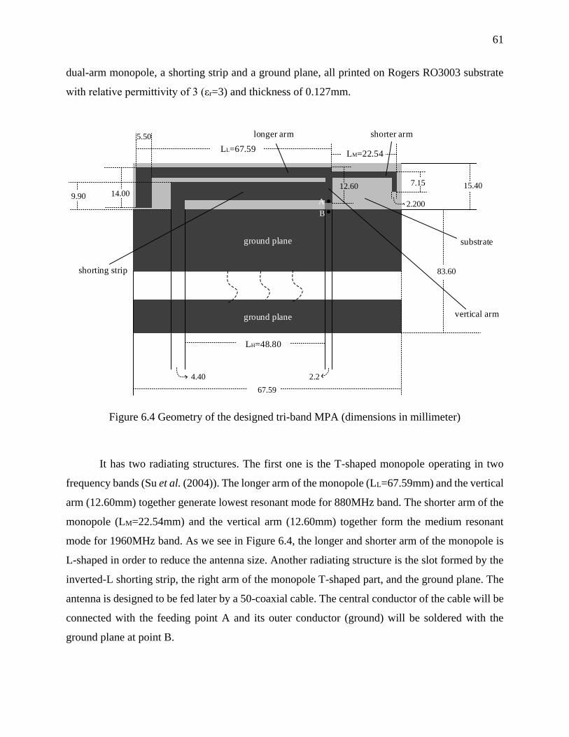
61
dual-arm monopole, a shorting strip and a ground plane, all printed on Rogers RO3003 substrate
with relative permittivity of 3 (εr=3) and thickness of 0.127mm.
It has two radiating structures. The first one is the T-shaped monopole operating in two
frequency bands (Su et al. (2004)). The longer arm of the monopole (LL=67.59mm) and the vertical
arm (12.60mm) together generate lowest resonant mode for 880MHz band. The shorter arm of the
monopole (LM=22.54mm) and the vertical arm (12.60mm) together form the medium resonant
mode for 1960MHz band. As we see in Figure 6.4, the longer and shorter arm of the monopole is
L-shaped in order to reduce the antenna size. Another radiating structure is the slot formed by the
inverted-L shorting strip, the right arm of the monopole T-shaped part, and the ground plane. The
antenna is designed to be fed later by a 50-coaxial cable. The central conductor of the cable will be
connected with the feeding point A and its outer conductor (ground) will be soldered with the
ground plane at point B.
Figure 6.4 Geometry of the designed tri-band MPA (dimensions in millimeter)
7.15
2.200
LM=22.54
15.40
83.60
LL=67.59
9.90 14.00
67.59
4.40 2.2
LH=48.80
5.50
ground plane substrate
ground plane
12.60
longer arm shorter arm
shorting strip
vertical arm
A
B

62
The antenna is built in Ansoft simulation software HFSS (High Frequency Structure
Simulator). Figure 6.5 shows the simulated return loss of the antenna. The low band has a return
loss of -25.43dB (point m1 in Figure 6.5), the medium band has -13.92dB (point m2 in Figure 6.5)
and high band has -12.73dB (point m3 in Figure 6.5). Figure 6.6 plot the simulated 3D radiation
patterns at 880MHz, 1960MHz and 2.45GHz, respectively. The peak antenna gains are 2.35dBi for
low band, 4.57dBi for medium band and 5.55dBi for high band.
The low return loss and good radiation pattern (donut shape) of the proposed antenna at
880MHz are observed through these simulation results. As the operating frequency increases the
“donut” directional is not preserved, because of the change the resonant length of antenna.
Although the return losses at 1960MHz and 2.45GHz are around -14dBm (worse performance than
880MHz band) and the directions of maximum radiation of 2.45GHz and 1960MHz bands are not
z-direction, this does not influence its capability of tri-frequency operation.
Since the proposed antenna is planar, the matching networks (on 880MHz, 1960MHz and
2.45GHz band respectively) and the antenna can be integrated on the same substrate, where the
fabricated chip of rectifier can also be mounted on. These are recommended for future works.
Figure 6.5 Simulated return loss of the designed antenna
0.78 1.00 1.25 1.50 1.75 2.00 2.25 2.50 2.67Freq [GHz]
-25.00
-20.00
-15.00
-10.00
-5.00
-0.19
dB
(S(1
,1))
HFSSDesign1XY Plot 6
m1
m2m3
Curve Info
dB(S(1,1))Setup1 : Sw eep
Name X Y
m1 0.8800 -25.4341
m2 1.9600 -13.9223
m3 2.4500 -12.7308
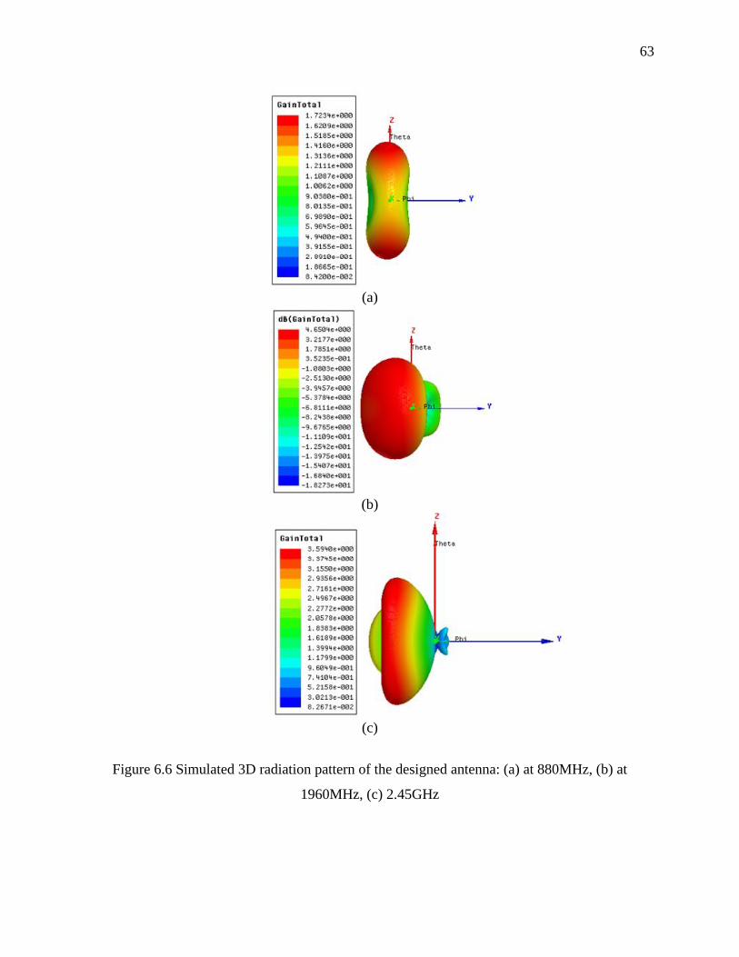
63
(a)
(b)
(c)
Figure 6.6 Simulated 3D radiation pattern of the designed antenna: (a) at 880MHz, (b) at
1960MHz, (c) 2.45GHz
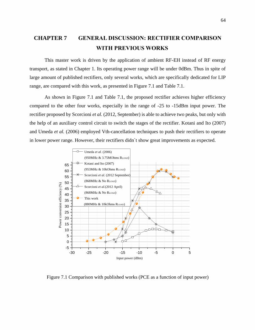
64
CHAPTER 7 GENERAL DISCUSSION: RECTIFIER COMPARISON
WITH PREVIOUS WORKS
This master work is driven by the application of ambient RF-EH instead of RF energy
transport, as stated in Chapter 1. Its operating power range will be under 0dBm. Thus in spite of
large amount of published rectifiers, only several works, which are specifically dedicated for LIP
range, are compared with this work, as presented in Figure 7.1 and Table 7.1.
As shown in Figure 7.1 and Table 7.1, the proposed rectifier achieves higher efficiency
compared to the other four works, especially in the range of -25 to -15dBm input power. The
rectifier proposed by Scorcioni et al. (2012, September) is able to achieve two peaks, but only with
the help of an auxiliary control circuit to switch the stages of the rectifier. Kotani and Ito (2007)
and Umeda et al. (2006) employed Vth-cancellation techniques to push their rectifiers to operate
in lower power range. However, their rectifiers didn`t show great improvements as expected.
-30 -25 -20 -15 -10 -5 0 5
-5
0
5
10
15
20
25
30
35
40
45
50
55
60
65
Pow
er c
onver
sion e
ffic
iency
(%
)
Input power (dBm)
Umeda et al. (2006)
(950MHz & 3.75MOhms RLOAD)
Kotani and Ito (2007)
(953MHz & 10kOhms RLOAD)
Scorcioni et al. (2012 September)
(868MHz & No RLOAD)
Scorcioni et al.(2012 April)
(868MHz & No RLOAD)
This work
(880MHz & 10kOhms RLOAD)
Figure 7.1 Comparison with published works (PCE as a function of input power)

65
Table 7.1: Comparison with published works (*calculated from figures)
Work Frequency
Minimum input
@ output load
resistance
Peak efficiency
@ input power Tchnology Others
Umeda et al.
(2006) 950MHz -15dBm*@3MΩ
11%
@ -6dBm input 0.3μm
External Vth-
cancelation technique
Kotani and Ito
(2007) 953MHz -20dBm*@10kΩ
29%
@ -9.9dBm 0.35μm N/A
Scorcioni et al.
(2012, April) 868MHz Not reported
45%
@ -7.5dBm* 0.13μm N/A
Scorcioni et al.
(2012, September) 868MHz
-17dBm*
@ no load
60%
@ -4dBm* 0.13μm
Two rectifiers
controlled by auxiliary
control circuit
This work 880MHz -26dBm @10kΩ 62%
@ -3dBm input 0.13μm
Low-threshold
transistors
Moreover, the efficiency of the proposed work is compared with the works of Kotani and
Ito (2007) and Hashemi et al. (2012) as a function of input magnitude with the same load condition,
as shown in Figure 7.2. The proposed rectifier is able to start operating at around 200mV input
magnitude. This remarkable improvement in overcoming dead-zone owes much to the employment
of LTV transistors.
200 400 600 800 1000 1200 1400 1600
-10
0
10
20
30
40
50
60
70
Pow
er c
onver
sion e
ffic
iency
(%
)
Magnitude of input voltage (mV)
This work (880MHz & 2kOhms RLOAD)
Hashemi et al. (2012)
(10MHz & 2kOhms RLOAD)
This work (880MHz & 10kOhms RLOAD)
Kotani and Ito (2007)
(953MHz & 10kOhms RLOAD)
Figure 7.2 Comparison with published works (PCE as a function of magnitude of Vin)

66
CONCLUSION
In this master thesis three CMOS rectifiers dedicated for ambient RF-EH have been
designed. Each rectifier consists of three stages of fully gate cross-coupled basic structure and
employs low-threshold-voltage transistors. The three rectifiers are fabricated on one single chip
using IBM 130nm CMOS technology. The measurement results show that they have great
capability of working at low input power range. They achieve peak efficiencies of 62%, 62% and
56.2% respectively for 880MHz, 1960MHz and 2.45GHz channel and they are capable of operating
at lower magnitude of input signal compared to certain published works.
In addition, a rectifier system with power combination at the output is proposed and
analyzed. The efficiency drop demonstrates the necessity of power management at higher input
range. Thus a power management block is proposed and simulated. The energy harvested from one
of the three channels is used to power up a comparator and an inverter, and the output of the
comparator picks up the higher output voltage between the other two channels to be connected with
the load.
Last but not least, a tri-band antenna is redesigned and simulated. Using a tri-band antenna
brings the benefit of lower volume of the overall RF-EH system. Simulation results show that it
gives relatively high gain and low return loss. Optimization and fabrication of this antenna are
recommended for future work.
To implement the proposed power management block is also recommended in the future
work. There are several critical issues about this topology. For example, the power consumption
of the comparator should be around several micro watts, and its response time or transmission delay
should be as low as possible, and the switches on the routes to the load should be designed carefully
to avoid severe voltage drop across them.
Three matching networks between the tri-band receiving antenna and the rectifier is
indispensable to reduce the transmission loss and also to increase the voltage at the input of the
rectifier. The transmitted power reaches its maximum when the antenna sees at its output
impedance that is the conjugate of its own impedance. High-Q components (for example: off-chip
inductors, capacitors, or transmission lines) are recommended to be exploited for impedance
matching in the first step due to their flexibility on change of values. Later, on-chip matching

67
network should be implemented since it is more preferable due to the trend of integrating all
discrete electronic components on chip.

68
REFERENCES
Agrawal, S., Pandey, S. K., Singh, J., & Parihar, M. S. (2014, March). Realization of efficient RF
energy harvesting circuits employing different matching technique. In Quality Electronic Design
(ISQED), 2014 15th International Symposium on (pp. 754-761). IEEE.
Ahmadi, M. M., & Jullien, G. (2005, August). A full CMOS voltage regulating circuit for
bioimplantable applications. In Circuits and Systems, 2005. 48th Midwest Symposium on (pp.
988-991). IEEE.
Alam, S. B., Ullah, M. S., & Moury, S. (2013, May). Design of a low power 2.45 GHz RF energy
harvesting circuit for rectenna. In Informatics, Electronics & Vision (ICIEV), 2013 International
Conference on (pp. 1-4). IEEE.
Andia Vera, G., Georgiadis, A., Collado, A., & Via, S. (2010, January). Design of a 2.45 GHz
rectenna for electromagnetic (EM) energy scavenging. In Radio and Wireless Symposium (RWS),
2010 IEEE (pp. 61-64). IEEE.
Arfin, S. K., & Sarpeshkar, R. (2012). An energy-efficient, adiabatic electrode stimulator with
inductive energy recycling and feedback current regulation.Biomedical Circuits and Systems,
IEEE Transactions on, 6(1), 1-14.
Atluri, S., & Ghovanloo, M. (2007, May). Incorporating back telemetry in a full-wave CMOS
rectifier for RFID and biomedical applications. In Circuits and Systems, 2007. ISCAS 2007. IEEE
International Symposium on (pp. 801-804). IEEE.
Bandyopadhyay, S., Mercier, P. P., Lysaght, A. C., Stankovic, K. M., & Chandrakasan, A. P. (2014,
February). 23.2 A 1.1 nW energy harvesting system with 544pW quiescent power for next-
generation implants. In Solid-State Circuits Conference Digest of Technical Papers (ISSCC), 2014
IEEE International (pp. 396-397). IEEE.
Based Characterization of a High-Coupled Screen Printed PZT Thick Film Unimorph Energy
Harvester. JOURNAL OF MICROELECTROMECHANICAL SYSTEMS, 23(4), 842-854.
Burasa, P., Constantin, N. G., & Wu, K. (2014). High-Efficiency Wideband Rectifier for Single-
Chip Batteryless Active Millimeter-Wave Identification (MMID) Tag in 65-nm Bulk CMOS
Technology.

69
Chiou, T. W., & Wong, K. L. (2002). Broad-band dual-polarized single microstrip patch antenna
with high isolation and low cross polarization. Antennas and Propagation, IEEE Transactions
on, 50(3), 399-401.
Dickson, J. F. (1976). On-chip high-voltage generation in MNOS integrated circuits using an
improved voltage multiplier technique. Solid-State Circuits, IEEE Journal of, 11(3), 374-378.
Do Valle, B., Wentz, C. T., & Sarpeshkar, R. (2011). An area and power-efficient analog li-ion
battery charger circuit. Biomedical Circuits and Systems, IEEE Transactions on, 5(2), 131-137.
Ghovanloo, M., & Atluri, S. (2008). An integrated full-wave CMOS rectifier with built-in back
telemetry for RFID and implantable biomedical applications. IEEE Trans. Circuits Syst. I, Reg.
Papers, 55(10), 3328-3334.
Ghovanloo, M., & Najafi, K. (2002). Fully integrated power supply design for wireless biomedical
implants. In Microtechnologies in Medicine & Biology 2nd Annual International IEEE-EMB
Special Topic Conference on (pp. 414-419). IEEE.
Ghovanloo, M., & Najafi, K. (2004). A modular 32-site wireless neural stimulation
microsystem. Solid-State Circuits, IEEE Journal of, 39(12), 2457-2466.
Hajati, A., & Kim, S. G. (2011). Ultra-wide bandwidth piezoelectric energy harvesting. Applied
Physics Letters, 99(8), 083105.
Hashemi, S., Sawan, M., & Savaria, Y. (2012). A high-efficiency low-voltage CMOS rectifier for
harvesting energy in implantable devices. Biomedical Circuits and Systems, IEEE Transactions
on, 6(4), 326-335.
Ho, J. S., Yeh, A. J., Neofytou, E., Kim, S., Tanabe, Y., Patlolla, B., ... & Poon, A. S. (2014).
Wireless power transfer to deep-tissue microimplants. Proceedings of the National Academy of
Sciences, 111(22), 7974-7979.
Hu, J., & Min, H. (2005, October). A low power and high performance analog front end for passive
RFID transponder. In Automatic Identification Advanced Technologies, 2005. Fourth IEEE
Workshop on (pp. 199-204). IEEE.
IBM cmrf8s Design Manual: CMOS8RF (CMRF8SF) Design Manual, ES#57P9006, November
30, 2010, IBM Corporation

70
IBM Training file: Foundry and Manufacturing Services Education, Design Kit and Technology
Training CMOS8RF (CMRF8SF) V1700, IBM Corporation
Jianyun, H., Yan, H., & Hao, M. (2005). High efficient rectifier circuit eliminating threshold
voltage drop for RFID transponders. In 2005 6th International Conference on ASIC (Vol. 2, pp.
607-610).
Karolak, D., Taris, T., Deval, Y., Begueret, J. B., & Mariano, A. (2012, December). Design
comparison of low-power rectifiers dedicated to RF energy harvesting. In Electronics, Circuits and
Systems (ICECS), 2012 19th IEEE International Conference on (pp. 524-527). IEEE.
Kishi, M., Nemoto, H., Hamao, T., Yamamoto, M., Sudou, S., Mandai, M., & Yamamoto, S. (1999,
August). Micro thermoelectric modules and their application to wristwatches as an energy source.
In Thermoelectrics, 1999. Eighteenth International Conference on (pp. 301-307). IEEE.
Kocer, F., & Flynn, M. P. (2006). A new transponder architecture with on-chip ADC for long-
range telemetry applications. Solid-State Circuits, IEEE Journal of, 41(5), 1142-1148.
Kotani, K., & Ito, T. (2007, November). High efficiency CMOS rectifier circuit with self-Vth-
cancellation and power regulation functions for UHF RFIDs. In Solid-State Circuits Conference,
2007. ASSCC'07. IEEE Asian (pp. 119-122). IEEE.
Laursen, L. (2012). Snails in a race for biological energy harvesting.Spectrum, IEEE, 49(5), 19-19.
Lee, K. F., & Tong, K. F. (2012). Microstrip Patch Antennas—Basic Characteristics and Some
Recent Advances. Proceedings of the IEEE, 100(7), 2169-2180.
Le, H., Fong, N., & Luong, H. C. (2010, August). RF energy harvesting circuit with on-chip
antenna for biomedical applications. In Communications and Electronics (ICCE), 2010 Third
International Conference on (pp. 115-117). IEEE.
Le, T., Mayaram, K., & Fiez, T. (2008). Efficient far-field radio frequency energy harvesting for
passively powered sensor networks. Solid-State Circuits, IEEE Journal of, 43(5), 1287-1302.
Le, T. T., Han, J., von Jouanne, A., Mayaram, K., & Fiez, T. S. (2006). Piezoelectric micro-power
generation interface circuits. Solid-State Circuits, IEEE Journal of, 41(6), 1411-1420
Li, B., Shao, X., Shahshahan, N., Goldsman, N., Salter, T., & Metze, G. M. (2013). An antenna
co-design dual band RF energy harvester.

71
Mandal, S., & Sarpeshkar, R. (2007). Low-power CMOS rectifier design for RFID applications.
Circuits and Systems I: Regular Papers, IEEE Transactions on, 54(6), 1177-1188.
Masuch, J., Delgado-Restituto, M., Milosevic, D., & Baltus, P. (2012, May). An RF-to-DC energy
harvester for co-integration in a low-power 2.4 GHz transceiver frontend. In Circuits and Systems
(ISCAS), 2012 IEEE International Symposium on (pp. 680-683). IEEE.
Ma, Y., Oliver, R. A., Humes, T. E., & Mavoori, J. (2014). U.S. Patent No. 8,759,937. Washington,
DC: U.S. Patent and Trademark Office.
Md Din, N., Chakrabarty, C. K., Bin Ismail, A., Devi, K. K. A., & Chen, W. Y. (2012). Design of
RF energy harvesting system for energizing low power devices. Progress In Electromagnetics
Research, 132, 49-69.
Nimo, A., Grgic, D., Ungan, T., & Reindl, L. M. (2013, October). A new family of passive wireless
RF harvesters based on RC-Quartz oscillators. In Microwave Conference (EuMC), 2013
European (pp. 511-514). IEEE.
Nishimoto, H., Kawahara, Y., & Asami, T. (2010, November). Prototype implementation of
ambient RF energy harvesting wireless sensor networks. InSensors, 2010 IEEE (pp. 1282-1287).
IEEE.
Oh, S., & Wentzloff, D. D. (2012, June). A− 32dBm sensitivity RF power harvester in 130nm
CMOS. In Radio Frequency Integrated Circuits Symposium (RFIC), 2012 IEEE (pp. 483-486).
IEEE.
Onizuka, K., Kawaguchi, H., Takamiya, M., Kuroda, T., & Sakurai, T. (2006, September). Chip-
to-chip inductive wireless power transmission system for SiP applications. In IEEE CICC
Proceedings (pp. 575-578).
Ouda, M. H., Arsalan, M., Marnat, L., Shamim, A., & Salama, K. N. (2013). 5.2-GHz RF Power
Harvester in 0.18-/spl mu/m CMOS for Implantable Intraocular Pressure Monitoring. Microwave
Theory and Techniques, IEEE Transactions on, 61(5), 2177-2184.
Papotto, G., Carrara, F., & Palmisano, G. (2011). A 90-nm CMOS threshold-compensated RF
energy harvester. Solid-State Circuits, IEEE Journal of, 46(9), 1985-1997.
72
Park, C., & Chou, P. H. (2006, September). Ambimax: Autonomous energy harvesting platform
for multi-supply wireless sensor nodes. In Sensor and Ad Hoc Communications and Networks,
2006. SECON'06. 2006 3rd Annual IEEE Communications Society on (Vol. 1, pp. 168-177). IEEE.
Pazin, L., Telzhensky, N., & Leviatan, Y. (2008). Multiband flat-plate inverted-F antenna for Wi-
Fi/WiMAX operation. IEEE antennas and wireless propagation letters, 7, 197-200.
Pinuela, M., Mitcheson, P. D., & Lucyszyn, S. (2013). Ambient RF energy harvesting in urban and
semi-urban environments. Microwave Theory and Techniques, IEEE Transactions on, 61(7),
2715-2726.
Russo, M., Šolić, P., & Stella, M. (2013). Probabilistic modeling of harvested GSM energy and its
application in extending UHF RFID tags reading range. Journal of Electromagnetic Waves and
Applications, 27(4), 473-484.
Salter, T., Choi, K., Peckerar, M., Metze, G., & Goldsman, N. (2009). RF energy scavenging
system utilising switched capacitor DC-DC converter. Electronics letters, 45(7), 374-376.
Scorcioni, S., Bertacchini, A., & Larcher, L. (2012, September). A 868MHz CMOS RF-DC power
converter with− 17dBm input power sensitivity and efficiency higher than 40% over 14dB input
power range. In ESSCIRC (ESSCIRC), 2012 Proceedings of the (pp. 109-112). IEEE.
Scorcioni, S., Larcher, L., & Bertacchini, A. (2012, April). Optimized CMOS RF-DC converters
for remote wireless powering of RFID applications. In RFID (RFID), 2012 IEEE International
Conference on (pp. 47-53). IEEE.
Scorcioni, S., Larcher, L., Bertacchini, A., Vincetti, L., & Maini, M. (2013, May). An integrated
RF energy harvester for UHF wireless powering applications. In Wireless Power Transfer (WPT),
2013 IEEE (pp. 92-95). IEEE.
Shameli, A., Safarian, A., Rofougaran, A., Rofougaran, M., & De Flaviis, F. (2007). Power
harvester design for passive UHF RFID tag using a voltage boosting technique. Microwave Theory
and Techniques, IEEE Transactions on, 55(6), 1089-1097.
Shokrani, M. R., Khoddam, M., Hamidon, M. N. B., Kamsani, N. A., Rokhani, F. Z., & Shafie, S.
B. (2014). An RF Energy Harvester System Using UHF Micropower CMOS Rectifier Based on a
Diode Connected CMOS Transistor. The Scientific World Journal, 2014.
73
Simjee, F., & Chou, P. H. (2006, October). Everlast: long-life, supercapacitor-operated wireless
sensor node. In Low Power Electronics and Design, 2006. ISLPED'06. Proceedings of the 2006
International Symposium on (pp. 197-202). IEEE.
Stoopman, M., Keyrouz, S., Visser, H. J., Philips, K., & Serdijn, W. A. (2013, June). A self-
calibrating RF energy harvester generating 1V at− 26.3 dBm. InVLSI Circuits (VLSIC), 2013
Symposium on (pp. C226-C227). IEEE.
Stoopman, M., Keyrouz, S., Visser, H. J., Philips, K., & Serdijn, W. A. (2014). Co-Design of a
CMOS Rectifier and Small Loop Antenna for Highly Sensitive RF Energy Harvesters.
Su, C. M., Chen, W. S., Cheng, Y. T., & Wong, K. L. (2004). Shorted T‐shaped monopole antenna
for 2.4/5 GHz WLAN operation. Microwave and optical technology letters, 41(3), 202-203.
Sun, H., Guo, Y. X., He, M., & Zhong, Z. (2012). Design of a high-efficiency 2.45-GHz rectenna
for low-input-power energy harvesting. Antennas and Wireless Propagation Letters, IEEE, 11,
929-932.
Takacs, A., Aubert, H., Fredon, S., Despoisse, L., & Blondeaux, H. (2014). Microwave Power
Harvesting for Satellite Health Monitoring.
Tallos, R. K., Wang, Z., & Volakis, J. L. (2014, July). Wi-Fi energy harvesting system using body-
worn antennas. In Antennas and Propagation Society International Symposium (APSURSI), 2014
IEEE (pp. 1405-1406). IEEE.
Tang, X., Lin, T., & Zuo, L. (2014). Design and optimization of a tubular linear electromagnetic
vibration energy harvester. Mechatronics, IEEE/ASME Transactions on, 19(2), 615-622.
Taris, T., Vigneras, V., & Fadel, L. (2012, June). A 900MHz RF energy harvesting module. In New
Circuits and Systems Conference (NEWCAS), 2012 IEEE 10th International (pp. 445-448). IEEE.
Theilmann, P. T., Presti, C. D., Kelly, D., & Asbeck, P. M. (2010, May). Near zero turn-on voltage
high-efficiency UHF RFID rectifier in silicon-on-sapphire CMOS. In Radio Frequency Integrated
Circuits Symposium (RFIC), 2010 IEEE (pp. 105-108). IEEE.
Thierry, T., Ludivine, F., Laurent, O., & Valerie, V. (2013, June). COTS-based modules for far-
field radio frequency energy harvesting at 900MHz and 2.4 GHz. In New Circuits and Systems
Conference (NEWCAS), 2013 IEEE 11th International (pp. 1-4). IEEE.

74
Umeda, T., Yoshida, H., Sekine, S., Fujita, Y., Suzuki, T., & Otaka, S. (2006). A 950-MHz rectifier
circuit for sensor network tags with 10-m distance. Solid-State Circuits, IEEE Journal of, 41(1),
35-41.
Visser, H. J., Reniers, A. C., & Theeuwes, J. A. (2008, October). Ambient RF energy scavenging:
GSM and WLAN power density measurements. InMicrowave Conference, 2008. EuMC 2008.
38th European (pp. 721-724). IEEE.
Visser, H. J., & Vullers, R. J. (2013). RF energy harvesting and transport for wireless sensor
network applications: Principles and requirements. Proceedings of the IEEE, 101(6), 1410-1423.
Vullers, R. J. M., van Schaijk, R., Doms, I., Van Hoof, C., & Mertens, R. (2009). Micropower
energy harvesting. Solid-State Electronics, 53(7), 684-693.
Wang, F., & Hansen, O. (2014). Electrostatic energy harvesting device with out-of-the-plane gap
closing scheme. Sensors and Actuators A: Physical,211, 131-137.
Wang, X., Jiang, B., Che, W., Yan, N., & Min, H. (2007, November). A high efficiency AC-DC
charge pump using feedback compensation technique. InSolid-State Circuits Conference, 2007.
ASSCC'07. IEEE Asian (pp. 252-255). IEEE.
Wang, Y., & Sawan, M. (2014). High-efficiency CMOS rectifier dedicated for multi-band ambient
RF energy harvesting. In Electronics, Circuits and Systems, 2014. ICECS 2014. 21st IEEE
International Conference. IEEE.
Wong, K. L., & Hsu, W. H. (2001). A broad-band rectangular patch antenna with a pair of wide
slits. Antennas and Propagation, IEEE Transactions on, 49(9), 1345-1347.
Yao, Y., Wu, J., Shi, Y., & Dai, F. F. (2009). A fully integrated 900-MHz passive RFID transponder
front end with novel zero-threshold RF–DC rectifier. Industrial Electronics, IEEE Transactions on,
56(7), 2317-2325.
Yi, J., Ki, W. H., & Tsui, C. Y. (2007). Analysis and design strategy of UHF micro-power CMOS
rectifiers for micro-sensor and RFID applications. Circuits and Systems I: Regular Papers, IEEE
Transactions on, 54(1), 153-166.

75
Yuan, H., Tang, X., Song, Q., Zhang, Y., Zhang, Y., Yang, F., & Niu, Y. (2015). Analytical models
of on-resistance and breakdown voltage for 4H-SiC floating junction Schottky barrier diodes.
Solid-State Electronics, 103, 83-89.

76
APPENDIX A – MA LAST METAL CROSS SECTION

77
APPENDIX B – SCHEMATIC VIEW OF THE DESIGNED 3-STAGE FGCC RECTIFIER

78
APPENDIX C – LAYOUT OF THE DESIGNED 3-STAGE FGCC RECTIFIER
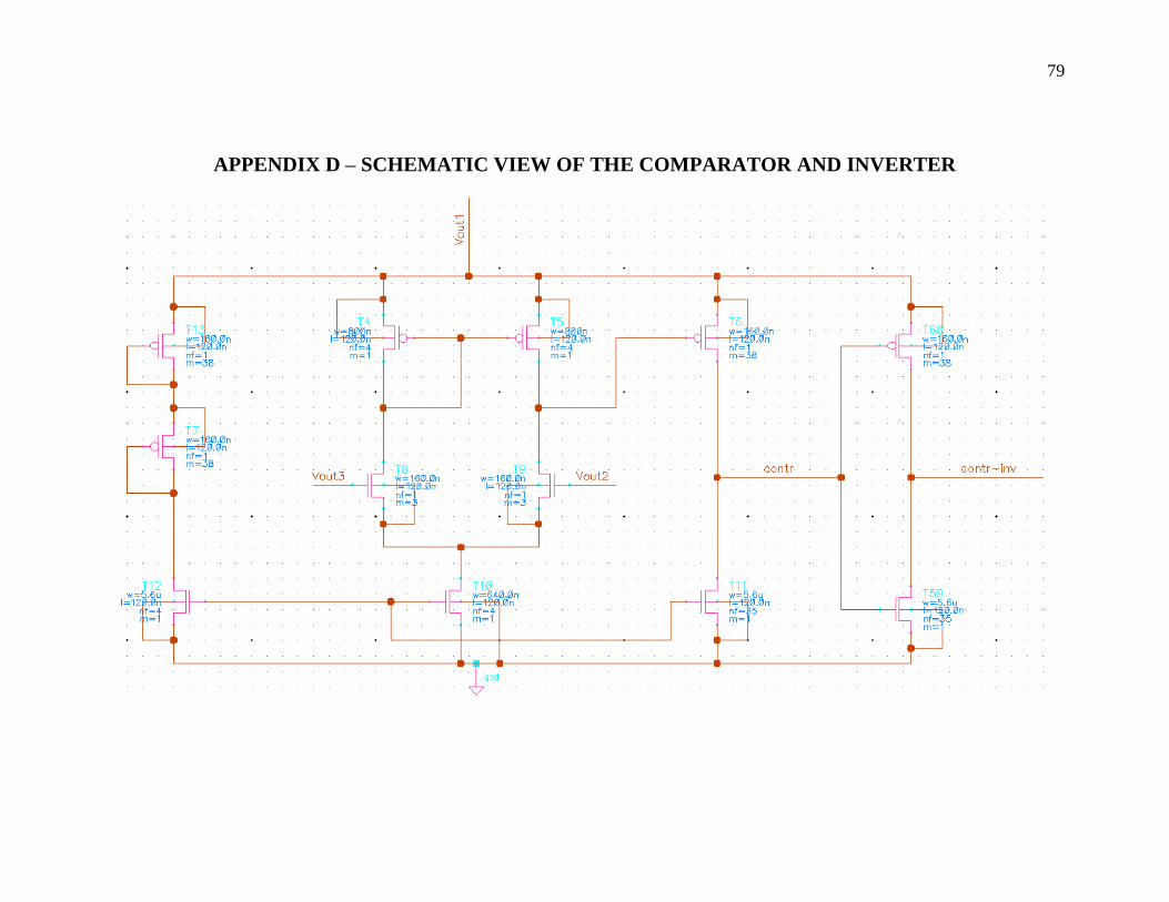
79
APPENDIX D – SCHEMATIC VIEW OF THE COMPARATOR AND INVERTER