PDF/1994/01/mmm 1994 5 1 31 0.pdf
10
31- Characterization of the metal-semiconductor interface by ballistic electron emission microscopy Roland Coratger, François Ajustron and Jacques Beauvillain CEMES-LOE / CNRS, 29 rue J. Marvig, BP. 4347, 31055 Toulouse, France (Received 20August, 1993, accepted 22 October,1993) Résumé. 2014 A travers les résultats obtenus sur des jonctions Au-Si(100), nous présentons les prin- cipales caractéristiques de la Microscopie par Emission d’Electrons Balistiques (BEEM). La spec- troscopie permet d’obtenir la hauteur de barrière Schottky locale avec une résolution de l’ordre du nanomètre à l’interface. La spectroscopie en mode "polarisation inverse" met en évidence un cou- rant de même sens qu’en polarisation directe. Ce courant peut être interprété en considérant que la diffusion par interaction entre porteurs est le phénomène dominant dans le transport d’électrons de faibles énergies. De plus, les variations du courant collecteur permettent l’imagerie BEEM. La hauteur de barrière Schottky étant constante sur ces échantillons, le contraste des images BEEM est principalement attribué à la diffusion dans le film métallique et à la qualité de l’interface. Abstract. 2014 Through the results obtained on Au-Si(100) junctions, we show the main aspects of Bal- listic Electron Emission Microscopy (BEEM). Spectroscopy allows the local Schottky barrier height to be yielded with a lateral resolution at the interface in the nanometer range. A collector current of electrons is evidenced in the reverse voltage condition. Carrier-carrier scattering is assumed to ac- count for this phenomenon and appears as the dominant process in low energy electron transport. In addition, collector current variations allow BEEM imaging. As the Schottky barrier height is found to be constant in these Au-Si(100) junctions, BEEM image contrast is mainly attributed to scattering in the gold film and interface quality. Microsc. MicroanaL Microstruct. FEBRUARY 1994, PAGE 31 Classification Physics Abstracts 61.16P - 68.20 - 73.40N 1. Introduction. Since its invention in 1981, the Scanning Tunneling Microscopy has proven to be a suitable tool for surface investigation [1]. Indeed, the exponential dependence of tunneling current in terms of tip-sample distance allows determination of the surface atomic structure with a resolution better than 0.1 nin. However, the informations only concem the first surface layers or, at the most, the layer just below the surface for certain reconstructions [2]. This lack has been partially filled after the pioneering work of Kaiser and Bell in 1988 [3, 4]. These authors have used a new technique, Ballistic Electron Emission Microscopy (BEEM), to study the buried interface between a metal and a semiconductor, i.e. a Schottky junction. This Article available at http://mmm.edpsciences.org or http://dx.doi.org/10.1051/mmm:019940050103100
Transcript of PDF/1994/01/mmm 1994 5 1 31 0.pdf
31-
Characterization of the metal-semiconductor interface by ballisticelectron emission microscopy
Roland Coratger, François Ajustron and Jacques Beauvillain
CEMES-LOE / CNRS, 29 rue J. Marvig, BP. 4347, 31055 Toulouse, France
(Received 20August, 1993, accepted 22 October,1993)
Résumé. 2014 A travers les résultats obtenus sur des jonctions Au-Si(100), nous présentons les prin-cipales caractéristiques de la Microscopie par Emission d’Electrons Balistiques (BEEM). La spec-troscopie permet d’obtenir la hauteur de barrière Schottky locale avec une résolution de l’ordre dunanomètre à l’interface. La spectroscopie en mode "polarisation inverse" met en évidence un cou-rant de même sens qu’en polarisation directe. Ce courant peut être interprété en considérant quela diffusion par interaction entre porteurs est le phénomène dominant dans le transport d’électronsde faibles énergies. De plus, les variations du courant collecteur permettent l’imagerie BEEM. Lahauteur de barrière Schottky étant constante sur ces échantillons, le contraste des images BEEM estprincipalement attribué à la diffusion dans le film métallique et à la qualité de l’interface.
Abstract. 2014 Through the results obtained on Au-Si(100) junctions, we show the main aspects of Bal-listic Electron Emission Microscopy (BEEM). Spectroscopy allows the local Schottky barrier heightto be yielded with a lateral resolution at the interface in the nanometer range. A collector current ofelectrons is evidenced in the reverse voltage condition. Carrier-carrier scattering is assumed to ac-count for this phenomenon and appears as the dominant process in low energy electron transport. Inaddition, collector current variations allow BEEM imaging. As the Schottky barrier height is foundto be constant in these Au-Si(100) junctions, BEEM image contrast is mainly attributed to scatteringin the gold film and interface quality.
Microsc. MicroanaL Microstruct. FEBRUARY 1994, PAGE 31
Classification
Physics Abstracts61.16P - 68.20 - 73.40N
1. Introduction.
Since its invention in 1981, the Scanning Tunneling Microscopy has proven to be a suitable toolfor surface investigation [1]. Indeed, the exponential dependence of tunneling current in terms oftip-sample distance allows determination of the surface atomic structure with a resolution betterthan 0.1 nin. However, the informations only concem the first surface layers or, at the most, thelayer just below the surface for certain reconstructions [2].
This lack has been partially filled after the pioneering work of Kaiser and Bell in 1988 [3, 4].These authors have used a new technique, Ballistic Electron Emission Microscopy (BEEM), tostudy the buried interface between a metal and a semiconductor, i.e. a Schottky junction. This
Article available at http://mmm.edpsciences.org or http://dx.doi.org/10.1051/mmm:019940050103100
32
Metal-Semiconductor (MS) contact leads to the well-know Schottky barrier which height eVB maybe estimated in a rough approximation as the metal work function 03A6M minus the electron affinityof the semiconductor Xs. The tip of the STM is then used as a very localized electron or holesource according to the voltage polarity. The carriers ballistically injected in a thin metal layermay overcome the potential barrier at the interface, provided their incident energy is sufficientand the metal thickness is comparable to the electron mean free path in the bulk material (typicallya few tens of nanometers for a few eV).BEEM spectroscopy therefore consists of the current detection in the semiconductor (le) in
terms of bias voltage V at a constant position (x, y) on the metal surface. The collector current isdifferent of zero when V is larger than VB and the threshold in the Ic (V) spectrum gives the localvalue of VB. An other possible mode of working is BEEM imaging. In this case, the tip-samplevoltage is kept constant at a value above the threshold. While scanning the metal surface with thetip, the vertical height of the tip and the local variations of the collector current in the semicon-ductor are simultaneously recorded. A BEEM image consists of a grey scale representation of thecurrent local variations.An other interesting aspect is the possible study of transport mechanism in thin metal layers.
Indeed, the local variations of Ic may originate from several mechanisms: scattering in the metallayer, interface defects, variations of the mean free path in terms of electron energy, injection intothe different minima of the semiconductor conduction band, ... that may be also studied with agreat accuracy by this method.
In this paper, we illustrate the possibilities of BEEM through the results obtained on thin goldfilms evaporated on Si(100). We discuss the effects of the electron scattering in the gold film andat the interface. Spectroscopy with reverse bias voltages also allows direct characterization ofcarrier-carrier scattering. BEEM images illustrate the non-homogeneity of these peculiar hetero-junctions.
2. Experimental.
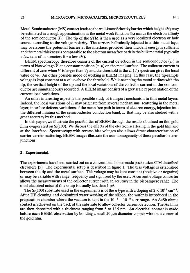
The experiments have been carried out on a conventional home-made pocket size STM describedelsewhere [5]. The experimental setup is described in figure 1. The bias voltage is establishedbetween the tip and the metal surface. This voltage may be kept constant (positive or negative)or may be variable with range, frequency and sign fixed by the user. A current-voltage converterallows the measurements of the collector current with an accuracy in the picoampere range. Thetotal electrical noise of this setup is usually less than 1 pA.The Si(100) substrate used in the experiments is of the n type with a doping of 2 x 1015 cm-3.
After HF cleaning and desionized water washing of the silicon, the wafer is introduced in thepreparation chamber where the vacuum is kept in the 10-8 - 10-9 torr range. An AuSb ohmiccontact is achieved on the back of the substrate to allow collector current detection. The Au filmsare then deposited with a thickness ranging from 5 to 12.5 nm. An electrical contact is madebefore each BEEM observation by bonding a small 50 03BCm diameter copper wire on a corner ofthe gold film.
33
Fig. 1. - Schema of the experimental setup with the STM tip and the Metal-Semiconductor junction. Thedrawing in the right-hand gives the energy diagram when the sample voltage is positive and larger than theSchottky barrier height at the interface.
3. Results.
3.1 SPECTROSCOPY.
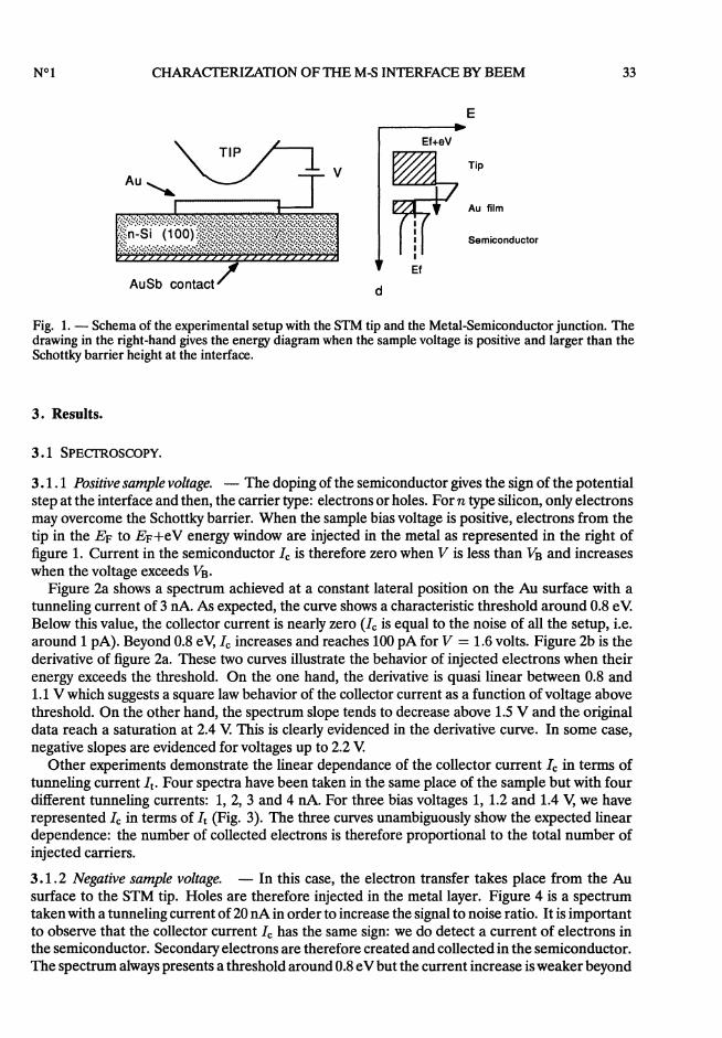
3.1.1 Positive sample voltage. - The doping of the semiconductor gives the sign of the potentialstep at the interface and then, the carrier type: electrons or holes. For n type silicon, only electronsmay overcome the Schottky barrier. When the sample bias voltage is positive, electrons from thetip in the EF to EF+eV energy window are injected in the metal as represented in the right offigure 1. Current in the semiconductor Ic is therefore zero when V is less than VB and increaseswhen the voltage exceeds VB.
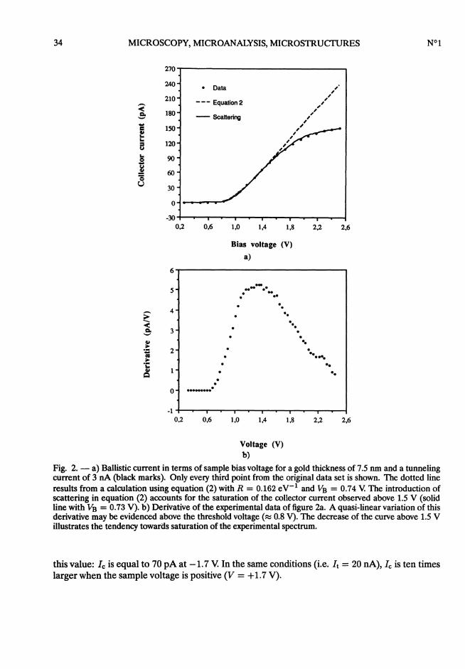
Figure 2a shows a spectrum achieved at a constant lateral position on the Au surface with atunneling current of 3 nA. As expected, the curve shows a characteristic threshold around 0.8 eVBelow this value, the collector current is nearly zero (le is equal to the noise of all the setup, i.e.around 1 pA). Beyond 0.8 eV, Ic increases and reaches 100 pA for V = 1.6 volts. Figure 2b is thederivative of figure 2a. These two curves illustrate the behavior of injected electrons when theirenergy exceeds the threshold. On the one hand, the derivative is quasi linear between 0.8 and1.1 V which suggests a square law behavior of the collector current as a function of voltage abovethreshold. On the other hand, the spectrum slope tends to decrease above 1.5 V and the originaldata reach a saturation at 2.4 V This is clearly evidenced in the derivative curve. In some case,negative slopes are evidenced for voltages up to 2.2 V
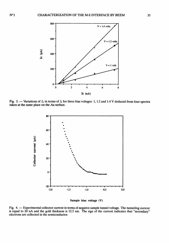
Other experiments demonstrate the linear dependance of the collector current Ic in terms oftunneling current It. Four spectra have been taken in the same place of the sample but with fourdifferent tunneling currents: 1, 2, 3 and 4 nA. For three bias voltages 1, 1.2 and 1.4 V, we haverepresented Ic in terms of It (Fig. 3). The three curves unambiguously show the expected lineardependence: the number of collected electrons is therefore proportional to the total number ofinjected carriers.
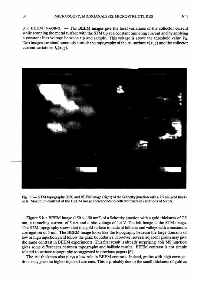
3.1.2 Negative sample voltage. - In this case, the electron transfer takes place from the Ausurface to the STM tip. Holes are therefore injected in the metal layer. Figure 4 is a spectrumtaken with a tunneling current of 20 nA in order to increase the signal to noise ratio. It is importantto observe that the collector current Ic has the same sign: we do detect a current of electrons inthe semiconductor. Secondary electrons are therefore created and collected in the semiconductor.The spectrum always presents a threshold around 0.8 eV but the current increase is weaker beyond
34
Fig. 2. - a) Ballistic current in terms of sample bias voltage for a gold thickness of 7.5 nm and a tunnelingcurrent of 3 nA (black marks). Only every third point from the original data set is shown. The dotted lineresults from a calculation using equation (2) with R = 0.162 eV-1 and VB = 0.74 V The introduction ofscattering in equation (2) accounts for the saturation of the collector current observed above 1.5 V (solidline with VB = 0.73 V). b) Derivative of the experimental data of figure 2a. A quasi-linear variation of thisderivative may be evidenced above the threshold voltage (~ 0.8 V). The decrease of the curve above 1.5 Villustrates the tendency towards saturation of the experimental spectrum.
this value: le is equal to 70 pA at -1.7 V. In the same conditions (i.e. It = 20 nA), 7c is ten timeslarger when the sample voltage is positive (V = +1.7 V).
35
Fig. 3. - Variations of Ic in terms of It for three bias voltages: 1, 1.2 and 1.4 V deduced from four spectrataken at the same place on the Au surface.
Fig. 4. - Experimental collector current in terms of negative sample tunnel voltage. The tunneling currentis equal to 20 nA and the gold thickness is 12.5 nm. The sign of the current indicates that "secondary"electrons are collected in the semiconductor.
36
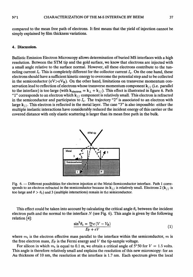
3.2 BEEM IMAGING. - The BEEM images give the local variations of the collector currentwhile scanning the metal surface with the STM tip at a constant tunneling current and by applyinga constant bias voltage between tip and sample. This voltage is above the threshold value VB.Two images are simultaneously stored: the topography of the Au surface z(x, y) and the collectorcurrent variations Ic (x, y).
Fig. 5. - STM topography (left) and BEEM image (right) of the Schottky junction with a 7.5 nm gold thick-ness. Maximum contrast of the BEEM image corresponds to collector current variations of 50 pA.
Figure 5 is a BEEM image (150 x 150 nm2) of a Schottky junction with a gold thickness of 7.5nm, a tunneling current of 5 nA and a bias voltage of 1.4 V The left image is the STM image.The STM topography shows that the gold surface is made of hillocks and valleys with a maximumcorrugation of 5 nm. The BEEM image looks like the topography because the large domains oflow or high injection yield follow the grain boundaries. However, several adjacent grains may givethe same contrast in BEEM experiments. This first result is already surprising: this MS junctiongives some différences between topography and ballistic results. BEEM contrast is not simplyrelated to surface topography as suggested in previous papers [6].The Au thickness also plays a low role in BEEM contrast. Indeed, grains with high corruga-
tions may give the higher injected currents. This is probably due to the small thickness of gold as
37
compared to the mean free path of electrons. It first means that the yield of injection cannot besimply explained by film thickness variations.
4. Discussion.
Ballistic Emission Electron Microscopy allows determination of buried MS interfaces with a highresolution. Between the STM tip and the gold surface, we know that electrons are injected witha small angle relative to the surface normal. However, all these electrons contribute to the tun-neling current It. This is completely different for the collector current le. On the one hand, theseelectrons should have a sufficient kinetic energy to overcome the potential step and to be collectedin the semiconductor (eV>eVB). On the other hand, limitations on transverse momentum con-servation lead to reflection of electrons whose transverse momentum component k// (i.e. parallelto the interface) is too large (with ketectron = kl + k//). This effect is illustrated in figure 6. Path"1" corresponds to an electron which k// component is relatively small. This electron is refractedin the semiconductor and participates to Ic. The trajectory "2" is associated to an electron withlarge k//. This electron is reflected in the metal layer. The case "3" is also impossible: either themultiple inelastic interactions have considerably reduced the incident energy of this carrier or thecovered distance with only elastic scattering is larger than its mean free path in the bulk.
Fig. 6. - Different possibilities for electron injection at the Metal-Semiconductor interface. Path 1 corre-sponds to an electron refracted in the semiconductor because its ka is relatively small. Electrons 2 (k// istoo large and e > (Je) and 3 (multiple interactions) remain in the semiconductor.
This effect could be taken into account by calculating the critical angle Be between the incidentelectron path and the normal to the interface N (see Fig. 6). This angle is given by the followingrelation [4]:
where mt is the electron effective mass parallel to the interface within the semiconductor, m îsthe free electron mass, EF is the Fermi energy and V the tip-sample voltage.
For silicon in which mt is equal to 0.1 m, we obtain a critical angle of 5°50 for V = 1.5 volts.This angle is therefore relatively small and explains the resolution of this new microscopy: for anAu thickness of 10 nm, the resolution at the interface is 1.7 nm. Each spectrum gives the local
38
electronic characteristic of the MS interface with this high resolution. The same properties applyto the BEEM images.
Interpretation of the experimental spectra has been furnished by Kaiser and Bell in their firstpaper on BEEM [3]. This one dimensional theoretical model has been later improved by twodimensional calculations [4]. The authors have used the formalism, introduced by Simmons in1963 for tunneling between planar electrodes [7], to describe both tunneling and collector current.Hence, the collector current may be written as:
where C is a constant, E_L and EII are the energy perpendicular and parallel to the interfacerespectively, f (E) is the Fermi-Dirac function and D (E..L) is the well-known expression for thetransmission probability of a square barrier. Emin and Emax are given by the energy and momentummatching conditions at the interface. R is a measure of attenuation due to scattering in the metallayer. In the calculations, the collector current only depends on two parameters: the Schottkybarrier height VB and R.We have used this formalism to fit the experimental data in the case of low bias voltages, i.e.
at the most 0.5 V above the threshold. The dotted line in figure 2a is a curve calculated by thisformalism with R = 0.162 eV-1 and VB = 0.74 V As expected, the model accounts for the spec-troscopic results in the low voltage case. Kaiser et al. [4] have also demonstrated the calculatedspectra have a square law behavior just above threshold as observed in the derivative of figure 2b.
Beyond these voltage values, equation (2) is less accurate: the calculated values are greaterthan the experimental data (see Fig. 2a above 1.5 V). The tendency to reach saturation in theexperimental spectra has been theoretically studied by Prietsch and Ludeke [8, 9]. These authorsadd in equation (2) a function that accounts for the variations with energy of the electron meanfree path (we have to kept in mind that R is an energy independent constant in (2)). Indeed, ithas been shown in previous works that, in the eV range, the mean free path Àe-e due to electron-electron scattering decreases when the energy increases [10]. In figure 2a, the solid line has beencalculated after introduction of inelastic scattering in the gold film in the form of an exponentialfunction. This example underlines the abilities of BEEM to study the transport properties of lowenergy electrons through thin metal layers.More generally, we have used the simplest formalism (2) to fit all the spectra yielded during the
experiments in the low energy range. Taken the accuracy of the method into account, i.e. around50 meV, we find the Schottky barrier height is constant for this MS interface (~ 0.77 eV). Thevariations of Ic rather arise from the fluctuations of the R parameter. This value is smaller thanthose usually obtained by BEEM on Si substrates [4] or by other techniques [11] (generally above0.8 eV).The same Schottky barrier height at the MS interface is still evidenced in the spectroscopy with
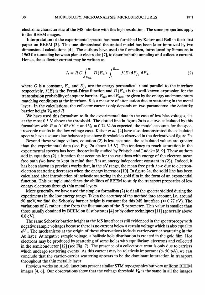
negative sample voltages because there is no current below a certain voltage which is also equal toeVB. The mechanisms at the origin of these observations include carrier-carrier scattering in theAu layer. At negative sample voltage, a ballistic hole distribution is created in the gold film. Hotelectrons may be produced by scattering of some holes with equilibrium electrons and collectedin the semiconductor [12] (see Fig. 7). The presence of a collector current is only due to carrierswhich undergo scattering events. As this current may be relatively important (> 50 pA), we canconclude that the carrier-carrier scattering appears to be the dominant interaction in transportthroughout the thin metallic layer.
Previous works on Au-Si junctions present similar STM topographies but very uniform BEEMimages [4, 6]. Our observations show that the voltage threshold VB is the same in all the images
39
Fig. 7. - Energy diagram for the scattering process (sample voltage negative and n-type semiconductor).For simplicity, the semiconductor band bending at the interface has been neglected. A ballistic hole dis-tribution is then created in the gold film. Hot electrons may be produced by scattering of some holes withequilibrium electrons and collected in the semiconductor.
and the injection yield locally varies which leads to the observed collector current variations. Someauthors have suggested that this could be due to variations of the injection angle on the grain edges[9]. In our case, this interpretation is not very convincing because the domains have an uniformcontrast even at the grain edges. Interface roughness may be invoked if one admits that adjacentgrains in a BEEM domain are located in areas where the interface normal has the same direction(because the BEEM domains follow the grain boundaries).We assume that the unusual large domains where low or high ballistic currents are observed,
may be attributed to interface domains rather than to different surface properties. Interface de-fects and intermigration are assumed to play an important role in the variations of injection yield[13]. Oxides on the Si(100) substrate are undoubtedly present before gold deposition. This couldaccount for the relative low barrier height observed during the spectroscopic measurements asreported in previous papers where techniques such as I (V ) or C(V ) measurements have beenused [14]. As suggested in [15], no BEEM current is observed when the interface oxide layer istoo thick. In this case, darker areas in the BEEM image could correspond to interface domainswith thicker oxide layers. This oxide layer, that considerably decreases the electron mean freepath at high kinetic energy, could also account for the saturation of the spectra at high voltage.
Interpretation of these BEEM images is therefore assumed to be tighly dependent of the in-terface quality, i.e. substrate cleanness before metal deposition, quality of the first métal layers,...Further experiments are necessary to resolve this problem. However, BEEM reveals the het-erogeneity of the MS junction and then appears to be of fundamental importance for Schottkyjunction optimization.
5. Summary.
In this paper, we show the possibilities of Ballistic Electron Emission Microscopy for Metal-Semiconductor interface characterization. Spectroscopy allows the Schottky barrier height to bedetermined with a lateral resolution at the interface in the nanometer range. For Au on Si(100),this barrier height is found to be constant with a value lower than usually obtained on similar junc-tions. Spectra realized in the reverse tip bias condition demonstrate that carrier-carrier scattering
40
is the dominant energy loss mechanism in transport through thin metallic layers. As the barrierheight is constant, BEEM images give the variations of the injection yield in the semiconductor.Large domains are mainly attributed to defects at the interface. All these results demonstrate thatBEEM appears as one of the most suitable tool to study buried interfaces.
Acknowledgements.
We would like to thank G. Peuch for technical assistance and F. Rossel for sample preparation.
References
[1] Binnig G., Rohrer H., Gerber Ch., Weibel E., Appl. Phys. Lett. 40 (1982) 178.[2] Binnig G., Rohrer H., Gerber Ch., Weibel E., Surf. Sci. 131 (1983) L379.[3] Bell L.D., Kaiser W.J., Scanning Microsc. 2 (1988) 1231.[4] Bell L.D., Kaiser W.J., Phys. Rev. Lett. 61 (1988) 2368.[5] Coratger R., Beauvillain J., Ajustron F., Lacaze J.C., Tremollieres C., Rev. Sci. Instrum. 62 (1991) 830.[6] Palm H., Arbes M., Schulz M., Appl. Phys. A56 (1993) 1.[7] Simmons J.G., 34 (1963) 1793.[8] Ludeke R., Prietsch M., Samsavar A., J. Vac. Sci. Technol. B9 (1991) 2342.[9] Ludeke R., Prietsch M., J. Vac. Sci. Technol. A9 (1991) 885.
[10] Quinn J.J., Phys. Rev. 126 (1962) 1453.[11] Brillson L.J., Surf. Sci. Rep. 2 (1982) 123.[12] Bell L.D., Hecht M.H., Kaiser W.J., Davis L.C., Phys. Rev. Lett. 64 (1990) 2679.[13] Cros A., Derrien J., Salvan F., Surf. Sci. 110 (1981) 471.[14] Rhoderick E.H., Williams R.H. (Clarendon, Oxford Press, 1988).[15] Hallen H.D., Fernandez A., Huang T., Buhrman R.A., Silcox J., J. Vac. Sci. Technol. B9 (1991) 585.