
New Small Wheel Low-Voltage Power: Design Review
26
New Small Wheel Low-Voltage Power: Design Review Jon Ameel a , Dan Amidei a , Karishma Sekhon Edgar a , Ryan Edgar a , Yunjie Yang a , Paolo Cova b,f , Nicola Delmonte b,f , Agostino Lanza b , Stefania Baccaro c , Salvatore Fiore c , Mauro Citterio d , Stefano Latorre d , Massimo Lazzaroni d,e a University of Michigan, Ann Arbor b Istituto Nazionale di Fisica Nucleare di Pavia c ENEA and INFN Sez di Roma d Istituto Nazionale di Fisica Nucleare di Milano e Universit` a degli Studi di Milano f Universit` a degli Studi di Parma February 5, 2015 1 Introduction This document details the present status of research and development for the low-voltage power systems of the ATLAS New Small Wheel (NSW). The combination of large power requirements and low available cabling space suggests a point-of-load conversion archi- tecture, where power is delivered to a front-end board (FEB) at a relatively high voltage (10V or more) and then reduced to the delivery voltage by on-FEB power electronics. This is potentially a multi-step process. Power will be delivered to the rim of the NSW at a voltage of at least 24V. From the rim, it will be distributed to the individual front-end boards. If the FEBs are unable to directly accept the voltage delivered to the rim, an additional conversion step is required at the point of distribution. This point of distribution is also a natural location for circuit protection and ballast resistors. On the FEBs, power conversion will be accomplished by single-inductor buck converters, optionally followed by one or more low-dropout regulators (LDOs) for noise reduction or to provide additional output voltages. The challenges in this approach are to ensure that the selected power conversion device(s) will: 1. Survive in the radiation and magnetic field environment of the NSW; 2. Effectively couple to the proposed cooling system; 3. Not introduce noise that may impact sensitive analog components; 1
Transcript of New Small Wheel Low-Voltage Power: Design Review
New Small Wheel Low-Voltage Power: Design Review
Jon Ameela, Dan Amideia, Karishma Sekhon Edgara, Ryan Edgara,Yunjie Yanga, Paolo Covab,f , Nicola Delmonteb,f , Agostino Lanzab,
Stefania Baccaroc, Salvatore Fiorec,Mauro Citteriod, Stefano Latorred, Massimo Lazzaronid,e
aUniversity of Michigan, Ann Arbor
bIstituto Nazionale di Fisica Nucleare di Pavia
c ENEA and INFN Sez di Roma
dIstituto Nazionale di Fisica Nucleare di Milano
eUniversita degli Studi di Milano
fUniversita degli Studi di Parma
February 5, 2015
1 Introduction
This document details the present status of research and development for the low-voltagepower systems of the ATLAS New Small Wheel (NSW). The combination of large powerrequirements and low available cabling space suggests a point-of-load conversion archi-tecture, where power is delivered to a front-end board (FEB) at a relatively high voltage(10 V or more) and then reduced to the delivery voltage by on-FEB power electronics.
This is potentially a multi-step process. Power will be delivered to the rim of theNSW at a voltage of at least 24 V. From the rim, it will be distributed to the individualfront-end boards. If the FEBs are unable to directly accept the voltage delivered to therim, an additional conversion step is required at the point of distribution. This pointof distribution is also a natural location for circuit protection and ballast resistors. Onthe FEBs, power conversion will be accomplished by single-inductor buck converters,optionally followed by one or more low-dropout regulators (LDOs) for noise reduction orto provide additional output voltages.
The challenges in this approach are to ensure that the selected power conversiondevice(s) will:
1. Survive in the radiation and magnetic field environment of the NSW;
2. Effectively couple to the proposed cooling system;
3. Not introduce noise that may impact sensitive analog components;
1
4. Fit within the relatively small available space on the FEBs;
5. Allow a cabling solution that fits within the available space for services.
This material is written primarily with reference to the MicroMegas, although it isrecognized that the chosen solution will likely be adopted by the sTGC detector as well.
2 Power Requirements and Design Constraints
The 7,500 front-end boards of the New Small Wheel are expected to require some 80 kWof delivered power (Tables 1b, 1a). Some 80% of this is for analog processing and digiti-zation (i.e. the VMM). The balance is required by communications and logic. The powerdemands are almost exclusively at very low voltages (1.2 V or 1.5 V).
The estimated power consumption of individual FE boards are shown in Table 1a.These estimates are based on the expected power consumption of the major componentson each board and an assumed average power-conversion efficiency of 64%. In the caseof ASICs whose development is not yet advanced, these values are speculative. Theremainder are taken from datasheets, or when possible from actual test results. Note thatthe pad trigger board is not included.
2.1 Radiation Load and Magnetic Field
The New Small Wheel is located sufficiently close to the interaction point that the radi-ation exposure is substantial over the NSW’s design lifetime. Ten-year radiation loads atthe inner and outer radii of the NSW are summarized in Table 2; the inner radius of thedetector is subject to some 20− 30× the radiation load of the outer radius.
Additionally, the New Small Wheel is within the fringing fields of the toroidal bendingmagnets. These are very well-understood from particle tracking studies. In the NSWvolume, the field ranges from negligible (inner radius) to over 5 kG (large sector corners).The majority of the NSW is subject to a field of less than 3 kG. This field is highlynonuniform; it is predominantly radial at high radii, but at intermediate radii becomesdominated by z and φ components.
2.2 Noise
On-detector power electronics are located within an extremely noise-sensitive environ-ment. The analog electronics require particular consideration, but the density of the finalinstallation and the potential for either conducted or radiated coupling between adjacentelectronics mandates that any additional noise from power conversion be minimized.
Traditionally, noise is minimized by a combination of heavy passive filtering and atwo-stage conversion process, where a DC-DC converter is followed by an LDO. TheLDO provides regulation and active attenuation of the high-frequency noise from the DC-DC converter. Including a LDO stage, however, has a negative impact on the overallpower conversion efficiency and entails the use of a further radiation-hard part. For that
2

Assumed Board Composition for Power Estimates
Part Power Qty. Per Board
(Watts) MM
FE
ADDC
L1DDC
Strip
Pad Rou
ter1
PadTrig
ger
VMM 0.840 8 5-7 2-3RO ASIC 0.630 1 1 1TDS ASIC 1.000 3-4 1-2ART ASIC 0.500 2SCA 0.250 1 1 1GBTX 2.200 2 1GBTIA 0.250 1GBTLD 0.325 2 1Current at 1.2 V 5.60 0.83 - 3.50 1.40
4.90 2.10Current at 1.5 V 0.59 2.93 1.47 2.09 1.25
2.51 1.67Current at 2.5 V ? 0.26 0.23 ? ?Total Power 7.60 6.05 2.78 7.34 3.56 16.00 10.00(Watts) -9.65 -5.031 Voltage rails for router: 1.0 V (x3), 1.2 V, 1.8 V, 2.5 V, 3.3 V
(a)
New Small Wheel Power Requirements
Device Number of Power1
Devices (Watts)MM
MMFE 4096 11.88ADDC 512 9.45L1DDC 512 4.34Total Power 55700
sTGCStrip (5 VMM) 128 11.47Strip (6 VMM) 384 12.78Strip (7 VMM) 256 15.08Pad+Wire (2 VMM) 512 7.86Pad+Wire (3 VMM) 256 5.56L1DDC 512 4.34Router 256 25.00Pad Trigger 32 15.63Total Power 237161 Assuming a 64% on-FEB conversion efficiency.
(b)
Table 1: Estimates for FE board power consumption. Table (a) shows the estimatefor each FEB. For those sTGC boards that accommodate different numbers of VMMs,multiple power estimates are shown. Also shown are estimates for the required current oneach voltage rail. These estimates assume a worst-case scenario where the RO companionand SCA chip both draw primarily 1.5 V. Table (b) shows the total power consumption ofthe NSW derived from these estimates. These numbers assume a 64% average efficiencyfor on-board power conversion; a solution without linear regulators would improve this to75%-80%.
3

Magnetic and Radiation Tolerance Criteria for COTS parts
Inner Rim (R = 1 m) Outer Rim (R = 5 m)TID (γ) 1740 Gy 84 GyNIEL (fast neutrons) 2.1× 10¹⁴ n/cm2 7.1× 10¹² n/cm2
SEE1 (protons) 4.3× 10¹³ p/cm2 1.4× 10¹² p/cm2
B field ≤1 kG 5 kG1 Simulated number of hadrons with E > 20 MeV
Table 2: Radiation and magnetic tolerance criteria. Radiation numbers assume 10 yearsat an LHC luminosity of L = 5× 1034 p/cm2s. Safety factors include are appropriate forhomogenous-batch COTS devices with control for dose-rate effects. A 30% increase canbe expected from the JD shielding redesign.
Power Supply Rejection1.2V l t
1.2V l tnoise regulator
input
regulator
input
noise
VMM amplifier
pMOSFET
VMM amplifier
pMOSFET
100
ne Gain 16 mV/fC
p p p pp y100
ne Gain 16 mV/fC
p p p pp yENC for filtered 1 nV/√HZ noise ENC for 1 µV rms in spectral line
1000
dwid
th B
Gain 16 mV/fC
p p p pp y1000
dwid
th B
Gain 16 mV/fC
p p p pp y
60
80 Peaktime 25 ns 50 ns 100 ns 200 ns
oise
on
spec
tral l
i
60
80 Peaktime 25 ns 50 ns 100 ns 200 ns
oise
on
spec
tral l
i
100
Peaktime 25 ns 50 ns 100 ns 200 ns
e no
ise
with
ban
d
100
Peaktime 25 ns 50 ns 100 ns 200 ns
e no
ise
with
ban
d
20
40
C p
er µ
V 1
rms
no
20
40
C p
er µ
V 1
rms
no
10
nV/s
qrt(H
z) w
hite
10
nV/s
qrt(H
z) w
hite
105 106 107 108 1090
EN
C
Frequency of spectral line [Hz]
105 106 107 108 1090
EN
C
Frequency of spectral line [Hz]
103 104 105 106 107 108 1091
EN
C fo
r 1
Noise bandwidth B [Hz]
103 104 105 106 107 108 1091
EN
C fo
r 1
Noise bandwidth B [Hz]
(a)
Power Supply Rejection1.2V l t
1.2V l tnoise regulator
input
regulator
input
noise
VMM amplifier
pMOSFET
VMM amplifier
pMOSFET
100
ne Gain 16 mV/fC
p p p pp y100
ne Gain 16 mV/fC
p p p pp yENC for filtered 1 nV/√HZ noise ENC for 1 µV rms in spectral line
1000
dwid
th B
Gain 16 mV/fC
p p p pp y1000
dwid
th B
Gain 16 mV/fC
p p p pp y
60
80 Peaktime 25 ns 50 ns 100 ns 200 ns
oise
on
spec
tral l
i
60
80 Peaktime 25 ns 50 ns 100 ns 200 ns
oise
on
spec
tral l
i
100
Peaktime 25 ns 50 ns 100 ns 200 ns
e no
ise
with
ban
d
100
Peaktime 25 ns 50 ns 100 ns 200 ns
e no
ise
with
ban
d
20
40
C p
er µ
V 1
rms
no
20
40
C p
er µ
V 1
rms
no
10
nV/s
qrt(H
z) w
hite
10
nV/s
qrt(H
z) w
hite
105 106 107 108 1090
EN
C
Frequency of spectral line [Hz]
105 106 107 108 1090
EN
C
Frequency of spectral line [Hz]
103 104 105 106 107 108 1091
EN
C fo
r 1
Noise bandwidth B [Hz]
103 104 105 106 107 108 1091
EN
C fo
r 1
Noise bandwidth B [Hz]
(b)
Figure 1: The noise sensitivity of the VMM2 [1]. Figure (a) shows the noise in terms ofequivalent noise charge per micro-volt RMS noise at a given frequency. Figure (b) showsthis integrated over a white noise spectrum up to the specified cutoff frequency.
reason, we also consider the possibility of direct power from an extremely low-noise DC-DC converter.
The VMM has demanding noise requirements for its analog supply. Figure 1 shows thesimulated sensitivity of the VMM2 to power supply noise. Figure (a) show the equivalentnoise charge (ENC) induced per microvolt noise at the given frequency. Figure (b) showsthe integral of the ENC assuming a white noise spectrum cutoff at a maximum frequencyB. Ideally, the ENC would be kept to 100 electrons or less [1]. This indicates that at themegahertz-scale frequencies associated with compact DC-DC converters, the noise at thefundamental frequency should be of the order of 1 µV.
4

MM – Water Cooling Channels
13/1/2015 Koulouris A. | Alexopoulos T. | Ciappeti M.
Lanza A. | Maltezos S. | Spigo G. 21
Wedge Top Corner 1 channel IN
∀ wedge side
=> 2 IN / wedge
4 IN / sector
16 sectors / NSW
128 IN / NSW
Distributed how?
3 cases follow
(solution depends
on infrastructure
availability)
Figure 2: The edge of a single MicroMegas quadruplet. Shown are the two parallel coolingchannels and the placement of an MMFE8 board. There is 6 mm between the component-side of an MMFE and its cooling channel. The distance between the reverse side and thenext cooling channel is slightly over 13 mm.
2.3 MicroMegas Cabling, Cooling and Mechanical
The most stringent space constraints are associated with the MicroMegas front-end boards(MMFE). These boards are situated along the edges of each MM plane; each board hosts8 VMM chips and supporting circuitry in order to provide digitization and readout ofdetector signals. Cooling channels, which also serve as cable raceways, are located betweenadjacent rows of MMFEs. This is shown in Figure 2.
The component-side of an MMFE faces its associated cooling channel, separated by agap of approximately 6 mm. The exact value will depend on the final choice of attachmentmethod for the MMFE. A machined cooling plate located in this gap will provide thermalcontact between the heat-generating components and the channel. The reverse side ofthe board is less constrained; the boards located on the inner two planes will have some13 mm between the reverse surface and the second cooling channel. If the final MMFEinstallation requires that the boards be inserted at an angle or offset from their finalposition, the effectively available height will be less.
The cooling scheme also constrains the LV power cabling to the FE boards. The opencavity in the cooling channel - 7 mm × 29.5 mm - is expected to house LV cabling, HV
5
Figure 3: An illustration of the cabling occupancy of the MicroMegas cooling channel.The closed cavity on the right carries the cooling water through the channel, while theopen cavity on the left is used as a cableway. The drawing is representative of the end ofthe channel furthest from the beamline, where cabling ccupancy is maximal.
cabling, and fibers for readout. If the FE boards are to have individual LV connections(ie. a star distribution topology), then after accounting for HV and fibers, the remainingspace allows for 22AWG cables (Fig. 3). The longest cable runs (4 m) would have aresistance of 212 mΩ. This can supply a current of 1 A at 12 V at 95% efficiency (e.g. a10 W MMFE8), which is sufficient in all scenarios for any of the FE boards that will becabled through the cooling channel.
Constraints on the board surface area available for power are less easily quantified.However, the MMFE will be extremely densely populated, and any reduction of the powerconversion area will help ease placement on and layout of the final board. As a point ofreference, roughly 1600 mm2-1700 mm2 is used for power conversion and regulation on theMMFE8 demonstrator. This area contains four DC-DC converters and twelve LDOs.
6

3 On-FEB Power Conversion Options
3.1 COTS Buck Converters, LDOs
Compact buck converters providing 1 V-2 V from greater than 12 V input are widely usedin consumer electronics and automotive applications. Low-dropout regulators are ubiq-uitous. Because the radiation loads in the New Small Wheel are relatively modest, thisallows the possibility that commercial-off-the-shelf (COTS) power conversion devices maybe suitable.
One advantage of this approach is cost, as COTS parts tend to be relatively inexpen-sive. A second and more important advantage is that the extensive commercial marketfor power conversion devices has produced a large collection of optimized solutions; manyhave desirable features that would ease board design and integration issues. A list ofcandidate devices was identified by a combination of market survey and recommenda-tion (Table 3). The selected candidate parts include such features as multiple outputs(LTM4619, LTM4628, ADP5052), low radiated noise (LTM8033), or integrated magnetics(LTM8033, LTM4619, LTM4628).
3.2 FEAST
Point-of-load conversion is an attractive solution for many particle physics applications.In recognition of the common constraints in these applications, an extensive researchand development effort in the CERN microelectronics group has undertaken to producea common solution. The product of this effort, the FEASTMP [2, 3], is a 4 A-capablesynchronous buck converter intended to provide POL regulation from a 5 V-12 V input.The FEAST ASIC is designed to withstand a total ionizing dose of 2× 10⁹ Gy and anintegrated particle fluence of above 5× 10¹⁴ n/cm2 (1MeV-eq). The device is resilientagainst single-event effects and capable of operating in magnetic fields in excess of 40 kG.
The FEAST is normally provided as a mezzanine module with a stack height of14.37 mm (Fig. 4). Much of the height is a result of the toroidal air-core power inductor,a necessity for operation in magnetic fields of tens of kiloGauss. The module’s connectoralso contributes substantially to the height. Additionally, the module requires cooling viaa pad located on the bottom of the module.
A lower-profile module, the FEASTMP-CLP, also exists. This module locates theconnector on the opposite side of the board to reduce the stack height to 9.4 mm. This isa combination of 8.4 mm module height and a 1 mm mandatory gap between the moduleand the host board. Cooling is similarly accomplished through a thermal pad on thebottom of the module.
3.3 TPS7H1101: TI Space-Qualified LDO
A recent development is the beginning of discussions with Texas Instruments regarding aCERN bulk purchase of the TPS7H1101, a TI low-dropout regulator intended for spaceapplications. This part is nominally available at 200USD in unit quantities. However, TI
7
(a)
(b)
FEASTMP_CLP datasheet – rev 1.0
CERN - 1 -
FEASTMP_CLP
Radiation and magnetic field tolerant 10W DC/DC converter module Description
FEASTMP_CLP is a modified version of the FEASTMP
module customized for applications needing a module stack height below 1cm. The connector used in FEASTMP has been replaced here with another one allowing for direct contact of the DCDC module with the receiving board: this decreases the overall stack height to below 1cm and removes the need for any mechanical interface, easing the integration of the module. However, the new connection scheme requires more handling care and a longer module.
Other than the replacement of the connector and the increase of the module length (to allow for an additional screw to secure the module to the receiving board), the module is identical to FEASTMP. For this reason, this datasheet does not repeat all the information reported for the FEASTMP but only the few mechanical differences. For all electrical characteristics, please refer to the FEASTMP datasheet that can be found in the public web page of the
DCDC converter project: http://project-dcdc.web.cern.ch.
Figure 1: View of the FEASTMP_CLP module fully assembled (right) and with shield removed (left).
Pin Configuration
Pin Number Function
1 PGood
12 En
7,8,9,10,11,18,19,20,21,22 Vout
4,5,6,15,16,17 Gnd
2,3,13,14 Vin
Module size, footprint, and stack height
The outline of the module, seen from above, is shown in Figure 2
together with all relevant sizes.
Figure 2: Top view of the FEASTMP_CLP module with mechanical
dimensions.
The 22-pin power connector is located to the left, close to one of
the three 2.1mm diameter holes giving the possibility to screw the
module to the receiving board for optimal mechanical attachment
and thermal contact. The highlighted rectangle in the middle of the
module represents the shield, which is 8mm high, under which the
ASIC, the main inductor and most of the other passives are
arranged. When mated, the bottom of the module stays about 1mm
above the receiving board – a thermal pad should be inserted in this
gap for cooling. Adding the 0.4mm thickness of the PCB and the 8
mm height of the shield, the full stack height is below 10mm.
Figure 3: Side view of the FEASTMP_CLP module with
mechanical dimensions. When mated, a gap of about 1mm exists
between the module and the receiving board. A thermal pad should
be inserted there for efficient cooling of the module.
(c)
FEASTMP_CLP datasheet – rev 1.0
CERN - 1 -
FEASTMP_CLP
Radiation and magnetic field tolerant 10W DC/DC converter module Description
FEASTMP_CLP is a modified version of the FEASTMP
module customized for applications needing a module stack height below 1cm. The connector used in FEASTMP has been replaced here with another one allowing for direct contact of the DCDC module with the receiving board: this decreases the overall stack height to below 1cm and removes the need for any mechanical interface, easing the integration of the module. However, the new connection scheme requires more handling care and a longer module.
Other than the replacement of the connector and the increase of the module length (to allow for an additional screw to secure the module to the receiving board), the module is identical to FEASTMP. For this reason, this datasheet does not repeat all the information reported for the FEASTMP but only the few mechanical differences. For all electrical characteristics, please refer to the FEASTMP datasheet that can be found in the public web page of the
DCDC converter project: http://project-dcdc.web.cern.ch.
Figure 1: View of the FEASTMP_CLP module fully assembled (right) and with shield removed (left).
Pin Configuration
Pin Number Function
1 PGood
12 En
7,8,9,10,11,18,19,20,21,22 Vout
4,5,6,15,16,17 Gnd
2,3,13,14 Vin
Module size, footprint, and stack height
The outline of the module, seen from above, is shown in Figure 2
together with all relevant sizes.
Figure 2: Top view of the FEASTMP_CLP module with mechanical
dimensions.
The 22-pin power connector is located to the left, close to one of
the three 2.1mm diameter holes giving the possibility to screw the
module to the receiving board for optimal mechanical attachment
and thermal contact. The highlighted rectangle in the middle of the
module represents the shield, which is 8mm high, under which the
ASIC, the main inductor and most of the other passives are
arranged. When mated, the bottom of the module stays about 1mm
above the receiving board – a thermal pad should be inserted in this
gap for cooling. Adding the 0.4mm thickness of the PCB and the 8
mm height of the shield, the full stack height is below 10mm.
Figure 3: Side view of the FEASTMP_CLP module with
mechanical dimensions. When mated, a gap of about 1mm exists
between the module and the receiving board. A thermal pad should
be inserted there for efficient cooling of the module.
(d)
Figure 4: The FEASTMP module. Figure (a) shows the full module, with shield re-moved, and with air-core inductor removed. Figure (b) shows the module’s dimensions.Figures (c) and (d) show the same for the lower-profile FEASTMP-CLP.
8

MAX8556 ADP1755
Figure 5: The physical specifications of one proposed package for the TI TPS7H1101.Shown for comparison are two COTS regulators, the ADP1755 and MAX8556.
has indicated that with less costly alternate packaging and a sufficiently large order, thepart might be available for as low as 20-30USD per device.
This device is radiation-hard, although it has not yet been tested to the levels requiredin the New Small Wheel. TI has agreed to test the device’s TID tolerance internally, andhas also provided samples so that the device’s tolerance to displacement damage may beevaluated as well. These tests are presently pending, but are likely to be successful.
Unfortunately, the TPS7H1101 die is physically large, which limits the available pack-ages. One proposed package is shown in Figure 5, along with two candidate COTSregulators. It is unlikely that the size will be reduced much from this proposed pack-age. Along with considerations of cost, this will likely mandate a minimal usage of LDOsshould this device be a recommended options.
9
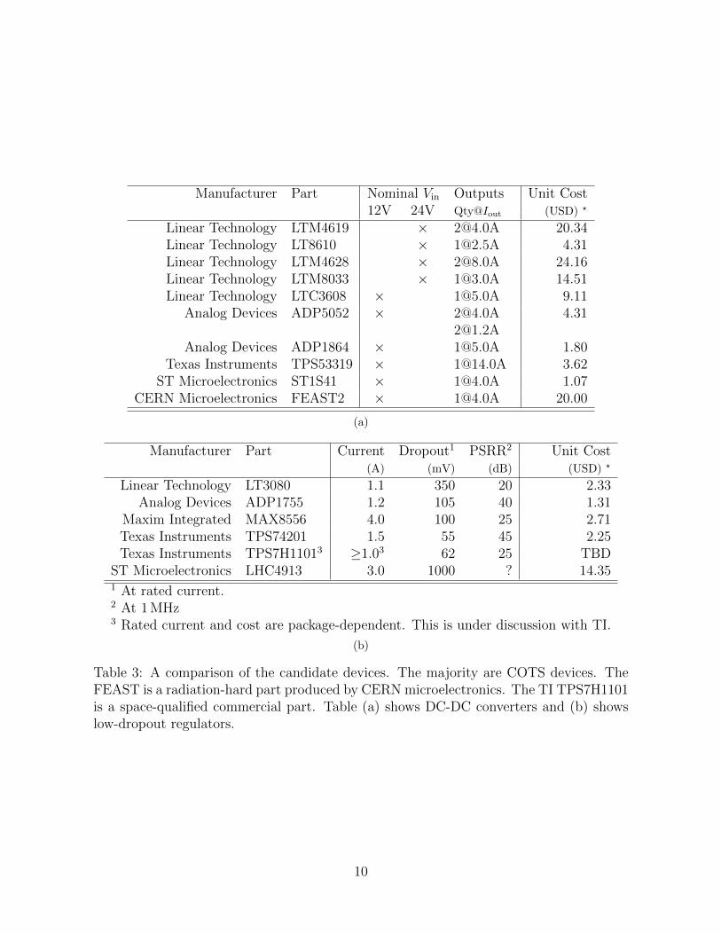
Manufacturer Part Nominal Vin Outputs Unit Cost12V 24V Qty@Iout (USD) ?
Linear Technology LTM4619 × [email protected] 20.34Linear Technology LT8610 × [email protected] 4.31Linear Technology LTM4628 × [email protected] 24.16Linear Technology LTM8033 × [email protected] 14.51Linear Technology LTC3608 × [email protected] 9.11
Analog Devices ADP5052 × [email protected]@1.2A
4.31
Analog Devices ADP1864 × [email protected] 1.80Texas Instruments TPS53319 × [email protected] 3.62
ST Microelectronics ST1S41 × [email protected] 1.07CERN Microelectronics FEAST2 × [email protected] 20.00
(a)
Manufacturer Part Current Dropout1 PSRR2 Unit Cost(A) (mV) (dB) (USD) ?
Linear Technology LT3080 1.1 350 20 2.33Analog Devices ADP1755 1.2 105 40 1.31
Maxim Integrated MAX8556 4.0 100 25 2.71Texas Instruments TPS74201 1.5 55 45 2.25Texas Instruments TPS7H11013 ≥1.03 62 25 TBD
ST Microelectronics LHC4913 3.0 1000 ? 14.351 At rated current.2 At 1 MHz3 Rated current and cost are package-dependent. This is under discussion with TI.
(b)
Table 3: A comparison of the candidate devices. The majority are COTS devices. TheFEAST is a radiation-hard part produced by CERN microelectronics. The TI TPS7H1101is a space-qualified commercial part. Table (a) shows DC-DC converters and (b) showslow-dropout regulators.
10

Part Rate Dose at Failure(Gy h−1) (Gray)
Candidate Buck ConvertersLTM8033 5 ≥ 40001,2
LT8610 10 ≥ 40002
LT8610 16 33003
LTM4628 16 15403
ADP5052 16 7503
ADP1864 16 6303
TPS53319 16 2603
ST1S41 16 2403
LTM4619 5 ≥ 40002
LTM4619 16 20003
LTM4619 22 23002
LTM4619 22 18002
LTM4619 50 3003
MAX8556 1500 24004,5
ADP1755 1500 23004
LT8612 1500 4004
Candidate Low-Dropout RegulatorsTPS74401 16 9103
LTM3083 16 9003
1 Deviations of above 20% in Vout observed during testing.2 ENEA Calliope.3 Brookhaven SSIF.4 High-rate TID data inferred from proton exposures (subsequent section).5 Device later regained functionality after annealing at room-temperatures.
Table 4: The dose of ionizing radiation at which failure was observed during 60Co ex-posures. The results are arranged in descending order by dose rate. The LTM4619 isdisplayed separately to illustrate the enhanced tolerance to ionizing radiation that is ev-ident at lower rates. This table also includes TID tolerance data obtained from protontesting. The extremely high dose rate likely reduces the measured TID tolerance comparedto the low-rate 60Co exposures.
4 COTS Radiation and Magnetic Field Testing
5 Ionizing Radiation (TID)
Although the total dose in the operating environment is large, it is accumulated over theNew Small Wheel’s ten-year design lifetime at a rate of only 20 mGy h−1. Because manymodern semiconductor technologies are known to exhibit some degree of annealing atroom temperature, the failure-dosages measured at high rates may not accurately reflectthe failure-dosage in the low-rate environment of the New Small Wheel. To minimize thiseffect, candidate devices were irradiated over the longest possible times.
Exposures were conducted at two 60Co sources: the Solid State Irradiation Facility(SSIF), a 4× 10¹³ Bq source operated by Brookhaven National Laboratory in the United
11

States; and Calliope, a 3× 10¹⁵ Bq source operated by ENEA Casaccia in Italy. Buckconverters were powered by 24 V during irradiation, while providing 1.5 V to either resis-tive loads or voltage regulators on their outputs. Voltage regulators in turn were suppliedby 1.5 V while providing 1.2 V to resistive loads. Input voltage, input current, and outputvoltage for each device were monitored for the entirety of each exposure.
Several irradiation campaigns were conducted at these facilities, ranging in durationfrom 1-40 days at rates between 5 Gy h−1 and 22 Gy h−1. The dosages at failure from theseand other tests are summarized in Table 4. One part, the LTM4619, has been tested at aparticularly large variety of dose rates, and the tolerance to ionizing radiation is seen toimprove markedly as the dose rate decreases. The LT8610 appears to be affected similarly,though here there are fewer data points.
6 Displacement Damage (NIEL)
Those parts that appeared to display sufficient tolerance to ionizing radiation were sub-sequently tested for susceptibility to displacement damage using fast neutrons. An initialexposure was conducted at the Fast Neutron Irradiation Facility (FNI), operated by theUniversity of Massachusettes, Lowell. An unpowered collection of modules that includedthe LTM8033, LTM4628 and LT8610 were exposed to a total fluence of 1× 10¹³ n/cm2
1 MeV (Si). The LTM4628 experienced a small (<10 mV) increase in output voltage. Theoutput voltage of the LTM8033 was shifted by 40%, from 1.5 V to 2.1 V. No observablechanges occurred in the LT8610.
A second exposure at FNI was conducted to a higher fluence with the samples powered.The two-hour exposure reached 5× 10¹⁴ n/cm2 1 MeV (Si) equivalent neutrons. Twelvedevices in total were irradiated: six LT8610, one LTM4628 and one LTM4619, along withfour voltage regulators. The devices were placed into a sealed aluminum cell and lowered6 m into the reactor water. Power and monitoring were supplied remotely from the surfacethrough sealed, watertight cable assemblies. The parts were provided with in-situ resistiveloads as above.
At a total fluence of 2.5× 10¹⁴ n/cm2 1 MeV (Si), the LTM4619 experienced abruptfailure. One voltage regulator, the LT3080, experienced failure at a fluence of 5× 10¹³ n/cm2
1 MeV (Si). The remaining modules survived the testing. The LT8610 and LTM4628displayed output voltage shifts of 30 mV-50 mV, which is likely a result of accumulateddamage to internal voltage references.
Finally, the modules that had been previously exposed to gamma radiation at Calliopewere subsequently exposed to neutrons at TAPIRO, a 5 kW research reactor with dry irra-diation channels operated by ENEA Casaccia. This exposure was conducted with devicesunder power to a total fluence of 1× 10¹³ n/cm2 1 MeV (Si). The LTM8033 remained op-erational through the test, but the output voltage shifted upward by 50%. The LTM4619failed completely after 8× 10¹² n/cm2, while the LT8610 was entirely unaffected. Thefailure of the LTM4619 is likely due to additional ionizing radiation accumulated duringthe fast neutron exposure. These results are summarized in Table 5.
12
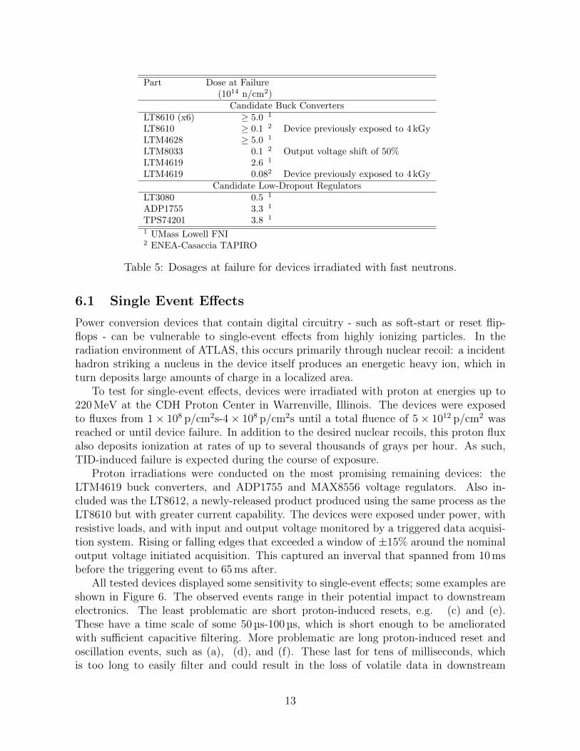
Part Dose at Failure(1014 n/cm2)
Candidate Buck ConvertersLT8610 (x6) ≥ 5.0 1
LT8610 ≥ 0.1 2 Device previously exposed to 4 kGyLTM4628 ≥ 5.0 1
LTM8033 0.1 2 Output voltage shift of 50%LTM4619 2.6 1
LTM4619 0.082 Device previously exposed to 4 kGyCandidate Low-Dropout Regulators
LT3080 0.5 1
ADP1755 3.3 1
TPS74201 3.8 1
1 UMass Lowell FNI2 ENEA-Casaccia TAPIRO
Table 5: Dosages at failure for devices irradiated with fast neutrons.
6.1 Single Event Effects
Power conversion devices that contain digital circuitry - such as soft-start or reset flip-flops - can be vulnerable to single-event effects from highly ionizing particles. In theradiation environment of ATLAS, this occurs primarily through nuclear recoil: a incidenthadron striking a nucleus in the device itself produces an energetic heavy ion, which inturn deposits large amounts of charge in a localized area.
To test for single-event effects, devices were irradiated with proton at energies up to220 MeV at the CDH Proton Center in Warrenville, Illinois. The devices were exposedto fluxes from 1× 10⁸ p/cm2s-4× 108 p/cm2s until a total fluence of 5× 10¹² p/cm2 wasreached or until device failure. In addition to the desired nuclear recoils, this proton fluxalso deposits ionization at rates of up to several thousands of grays per hour. As such,TID-induced failure is expected during the course of exposure.
Proton irradiations were conducted on the most promising remaining devices: theLTM4619 buck converters, and ADP1755 and MAX8556 voltage regulators. Also in-cluded was the LT8612, a newly-released product produced using the same process as theLT8610 but with greater current capability. The devices were exposed under power, withresistive loads, and with input and output voltage monitored by a triggered data acquisi-tion system. Rising or falling edges that exceeded a window of ±15% around the nominaloutput voltage initiated acquisition. This captured an inverval that spanned from 10 msbefore the triggering event to 65 ms after.
All tested devices displayed some sensitivity to single-event effects; some examples areshown in Figure 6. The observed events range in their potential impact to downstreamelectronics. The least problematic are short proton-induced resets, e.g. (c) and (e).These have a time scale of some 50 µs-100 µs, which is short enough to be amelioratedwith sufficient capacitive filtering. More problematic are long proton-induced reset andoscillation events, such as (a), (d), and (f). These last for tens of milliseconds, whichis too long to easily filter and could result in the loss of volatile data in downstream
13

−10
010
2030
4050
60
Tim
e(m
s)
0.0
0.5
1.0
1.5
2.0
Vout(Volts)
LT86
12.1
0T
ran
sien
t15
230
(a)
−5
05
1015
Tim
e(m
s)
0.0
0.5
1.0
1.5
2.0
2.5
3.0
Vout(Volts)
LTM
4619
.9T
ran
sien
t9
(b)
0.0
0.2
0.4
0.6
0.8
1.0
1.2
Tim
e(m
s)
0.0
0.5
1.0
1.5
2.0
Vout(Volts)
MA
X85
56.5
Tra
nsi
ent
85
(c)
0.0
0.2
0.4
0.6
0.8
1.0
1.2
Tim
e(m
s)
0.0
0.5
1.0
1.5
2.0
Vout(Volts)
MA
X85
56.7
Tra
nsi
ent
7660
(d)
05
1015
2025
Tim
e(m
s)
0.0
0.5
1.0
1.5
2.0
Vout(Volts)
AD
P17
55.6
Tra
nsi
ent
2464
0
(e)
05
1015
2025
Tim
e(m
s)
0.0
0.5
1.0
1.5
2.0
Vout(Volts)
AD
P17
55.7
Tra
nsi
ent
1132
14
(f)
Fig
ure
6:E
xam
ple
sof
singl
e-ev
ent
effec
tsob
serv
edin
220
MeV
pro
tons.
Fig
ure
(a)
show
stw
opro
ton-i
nduce
dre
sets
inan
LT
8612
occ
uri
ng
inra
pid
succ
essi
on.
Fig
ure
(b)
show
na
susp
ecte
ddes
truct
ive
singl
e-ev
ent
effec
tin
anLT
M46
19.
Fig
ure
s(c
)an
d(d
)sh
owpro
ton-i
nduce
dre
sets
and
osci
llat
ions
inth
eM
AX
8556
.F
igure
s(e
)an
d(f
)sh
owsi
milar
even
tsfo
rth
eA
DP
1755
.
14

Device Proton Energy Cross-Section Notes(MeV) 10−12cm−2
ADP1755 220 277 ± 8 Short transients220 83 ± 4 Long transients
MAX8556 ≥401 71 ± 4 Short transients≥401 0.50± 0.35 Long oscillations3
LTM4619 220 62 DestructiveLT8612 220 680 ±50 Multi-millisecond dropsMAX8556 220 2 ± 1 Long oscillations3
MAX8556 220 83 ± 8 Short transientsMAX8556 170 64 ± 9 Short transientsMAX8556 120 76 ± 9 Short transientsMAX8556 70 58 ±10 Short transientsMAX8556 40 58 ±10 Short transientsMAX8556 20 13 ± 3 Short transients
1 Combined result from individual measurements in the second part of the table.2 One event; no error is assigned.3 These were observed only at 220 MeV, and not in lower-energy exposures.
Table 6: Measured single-event cross-sections for buck converters and voltage regulatorsirradiated in a proton beam.
electronics (e.g. configuration registers). Most troubling is (b), which appears to be adestructive single-event effect in an LTM4619.
The measured cross-sections for these devices are shown in Table 6. As a point of ref-erence, at a distance of 1 m from the interaction point, a cross-section of 7.3× 10⁻¹⁴ cm−2
is equivalent to one SEE per device per year and a cross-section of 2.7× 10⁻¹¹ cm−2 equiv-alent to one SEE per device per day. At these levels, only the MAX8556 appears to beusable in all regions of the NSW. The observation of destructive single-event effects inthe LTM4619 entirely preclude its use. The LT8612’s large cross-section would result inseveral resets per day for devices located at r = 1 m.
6.2 Magnetic Field Tolerance
Several of the candidate parts are packaged modules that include integrated magnetics(LTM8033, LTM4619, LTM4628). This is desirable from the standpoint of system inte-gration, as it reduces the parts count and the footprint for the power circuitry while atthe same time simplifying the design of the front-end boards. However, the 0.3 T-0.6 Tmagnetic fields in the New Small Wheel are large enough to potentially saturate magneticmaterials.
These modules were tested for their ability to tolerate these magnetic fields at a 1 Tconventional electromagnet housed at the Laboratorio Acceleratori e SuperconduttiviataApplicata, operated by INFN and the University of Milan (see also Ref. [4, 5]). TwoLTM8033 and one LTM4619 were exposed to magnetic fields in three different orientations(Figure 7). The LTM8033, which includes additional magnetic shielding to suppress RFinterference, was able to operate in fields as high as 1 T with only small reductions in
15

0.00
0.10
0.20
0.30
0.40
0.50
0.60
0.70
0.80
0.90
0.0 0.1 0.2 0.3 0.4 0.5 0.6 0.7 0.8 0.9 1.0 1.1
Effic
ienc
y
B (T)
LTM8033 #1, B orthogonal (Z)
LTM8033 #1, B from right (X)
LTM8033 #1, B from top (Y)
LTM8033 #2, B orthogonal (Z)
LTM8033 #2, B from right (X)
LTM8033 #2, B from top (Y)
LTM4619 B orthogonal (Z)
LTM4619 B from right (X)
LTM4619 B from top (Y)
Figure 7: The efficiency of the LTM8033 and LTM4619 packaged modules as a functionof magnetic field strength. These modules include integrated magnetics, and thereforemay be affected by external magnetic fields.
efficiency. The LTM4619 tolerated fields as high as 0.5 T when the field was perpendicularto the plane of the board, but was only able to function to 0.3 T with the field parallel.
6.3 Summary
Table 7 displays the most limiting known tolerance for each of the tested commercialdevices. Although several COTS parts appeared promising in test of TID and NIELtolerance, subsequent tests for single-event effects in protons have uncovered several trou-bling behaviors. This suggests against the use of these devices on electronics that willbe located near the inner radius of the NSW. The potential exception is the MaximMAX8556, however, this part requires additional testing to demonstrate its tolerance todisplacement damage.
Although most of the COTS devices cannot be recommended for use in the high-radiation inner radii, the potential remains that some may be of use in the lower-radiationregion on the outer edge of the New Small Wheel. The large magnetic field there precludesthe use of the devices with integrated inductors. However, the Linear Technology LT8612is likely viable in this region, particularly if measures such as multiply-redundant devicesare taken to mitigate the single-event resets.
7 COTS Inductors
Although some of the candidate DC-DC converters include integrated magnetics, mostrequire external power inductors. In addition, smaller inductors will be used extensivelyfor filtering. In many cases this could be done with air-core inductors, however, the spacesaved by more compact ferrites is of value on the densely-populated front-end boards.
16

Test Notes
Part Limiting ToleranceCandidate Buck Converters
LTM4619 B 3 kGSEE destructive
LT8610 Iout 2 ALT8612 SEE σSE = 6.8× 10⁻¹⁰ cm−2
LTM4628 B 3 kGLTM8033 NIEL 1013 n/cm2
LTC3608 NIEL 1013 n/cm2
ADP5052 TID 750 GyADP1864 TID 630 GyTPS53319 TID 260 GyST1S41 TID 240 Gy
Candidate Low-Dropout RegulatorsLT3080 NIEL 5× 10¹³ n/cm2
ADP1755 SEEMAX8556 viable?TPS74201 engineering (Vbias)
Neutron dosages in 1 MeV (Si) equivalent.
Table 7: A summary of the limiting tolerances of the devices of interest. In all casesexcept the MAX8556, expected radiation doses near the inner rim of the NSW exceedthese tolerances. Some devices (e.g. the LT8612) appear suitable for usage on the outerrim.
Ferrite inductors, however, suffer from a loss of inductance when subject to externalmagnetic fields.
A testing program was conducted to locate ferrite-cored inductors, both for power andfor filtering, that are sufficiently tolerant of magnetic fields for use in the New Small Wheel.The results are shown in Table 9. Numerous inductors from several manufacturers weretested in a Neodymium-Iron-Boron magnet fixture able to produce fields up to 6.5 kG.The performance of the inductors was characterized by measuring their inductance as afunction of the external field strength. Molded inductors, in which the coil is sinteredinto a block of powdered iron, were typically the best performers. While most otherinductor geometries fall to 5-20% of their initial inductance in a 6.5 kG field, severalmolded inductors were found that retain nearly 50% of their inductance at these fieldstrengths.
8 Adapting the FEAST
The mechanical constraints of the FEASTMP and FEASMP-CLP modules are challeng-ing. While the latter can meet the height constraints for the MMFE, the module’s re-quirements that cooling be provided from the bottom pad does not readily integrate withthe MicroMega’s cooling system. Additionally, the 1 mm space between the module andFEB produces dead space on the FEB, where component placement becomes difficult or
17

(a) (b)
Figure 8: A prototype ultra-low-profile FEAST-based DC-DC converter. The protypewas constructed as a module compatible with the original FEAST for convenient testing.The shield was constructed from heavy-gauge copper to allow the shield to serve as analternate cooling path. The area required when integrated on a PCB is 16 mm × 27 mm.The height is 4 mm, but could be reduced further.
impossible.One option to address these constraints is to integrate the FEAST directly on the
FEBs using low-profile B-tolerant ferrite inductors. This avoids the small but noticablevoltage drop from the connector, minimizes the total height, and allows for the possibleuse of alternate cooling paths. To explore this usage of the FEAST ASIC, an ultra-low-profile module was constructed (Fig. 8). The design was produced as a module, and sharesthe same footprint as the original FEAST module for convenience in testing.
This implementation uses a surface-mount ferrite inductor identified during previoustests as being able to withstand magnetic fields as high as 6.5 kG. Integrated onto thefront-end boards, the required area per converter would be 430 mm2. The total heightis only 4 mm, and with alternate choices of power inductor could be reduced to below3 mm. Like the full-height FEAST module, a copper shield is included to reduce radiatedemissions.
8.1 Electrical Performance
The regulation, efficiency, and noise of the module were characterized on the benchtopwhile providing 1.5 V output from a 10 V input voltage.
The regulation is shown in Figure 9a as the difference between the output voltage atthe given current and the output voltage with no load. Curves are shown as measuredon the load side of the connector (representative of use as a module) and as measuredon the module itself (representative of direct integration on to a FEB). The differenceseen between these two measurements is due to the series resistance of the module’sconnector. A corresponding plot of the efficiency is shown in Figure 9b. Here, the slightlylower resistance of the surface-mount ferrite as compared to the air-core toroid producesa slight increase in efficiency.
Extensive study was also performed by the FEAST designers to reduce the conductednoise on the converter’s input and output [6, 7]. That work has been heavily drawn onhere. The module’s conducted noise was measured at load currents up to 4 A. Some noise
18

-‐80
-‐70
-‐60
-‐50
-‐40
-‐30
-‐20
-‐10 0
0.0
0.5
1.0
1.5
2.0
2.5
3.0
3.5
4.0
Delta Vout (mV)
Output Current (A)
Through Samtec connector
On module
FEAST Vout = 1.5V
(a)
60
65
70
75
80
85
90 1.0
1.5
2.0
2.5
3.0
3.5
4.0
Ef#iciency (%)
Output Current (A)
Through Samtec connector
On module
FEAST Vout = 1.5V
(b)
(c)
(d)
Fig
ure
9:R
egula
tion
(a),
effici
ency
(b),
and
conduct
ednoi
sem
easu
rem
ents
ofth
eult
ra-l
ow-p
rofile
FE
AST
module
(blu
ecu
rves
).A
sa
com
par
ison
,th
efu
ll-h
eigh
tF
EA
ST
module
wit
hai
r-co
reto
roid
isal
sosh
own
(red
curv
e).
Con
duct
ednoi
seis
show
nat
load
curr
ents
of1
A(c
)an
d2
A(d
).N
ote
that
the
pea
ks
bel
owth
e1.
63M
Hz
ripple
freq
uen
cyar
enoi
sefr
omth
ete
sten
vir
onm
ent.
19

(a) (b) (c)
Figure 10: Tles.
results from the prototype module are shown in Figures 9c and 9d, with the converterproviding 1 A and 2 A respectively. The latter was the noisiest case observed over thefull output current range, with an amplitude of 40 µV on the output at the converter’s1.63 MHz switching frequency. Although in isolation this does not yet meet the demand-ing VMM noise requirements, it was achieved with relatively modest component values.Larger filter components or the addition of another filtering stage can readily reduce itmuch further.
8.2 Cooling
To evaluate different cooling strategies, the ultra-low-profile FEAST included multiplecooling paths: a cooling pad located underneath the test board (Fig. 10b), a copperfinger on top of the test board (Fig. 10c), and the shield (Fig. 10a), which was designedto double as a heat-transfer mechanism.
The cooling paths were characterized by measuring the thermal resistance betweenthe ASIC case and a heatsink in good thermal contact (a copper bar). The case thermo-couple was attached with thermal epoxy to ensure good thermal contact. This method isimperfect, but provides a useful comparison. At present, methods are being investigatedto measure the die temperature directly.
The results of these measurements are shown in Table 8. A corresponding measure-ment of the full-height FEAST provides a point of comparison. Additionally, the mea-surements were repeated after filling the shield completely with thermal grease. In bothcases the underside cooling pad is the most effective solution. However, the injection ofthermal grease improved the heat transfer performance markedly, and can allow adequatecooling through the shield.
20
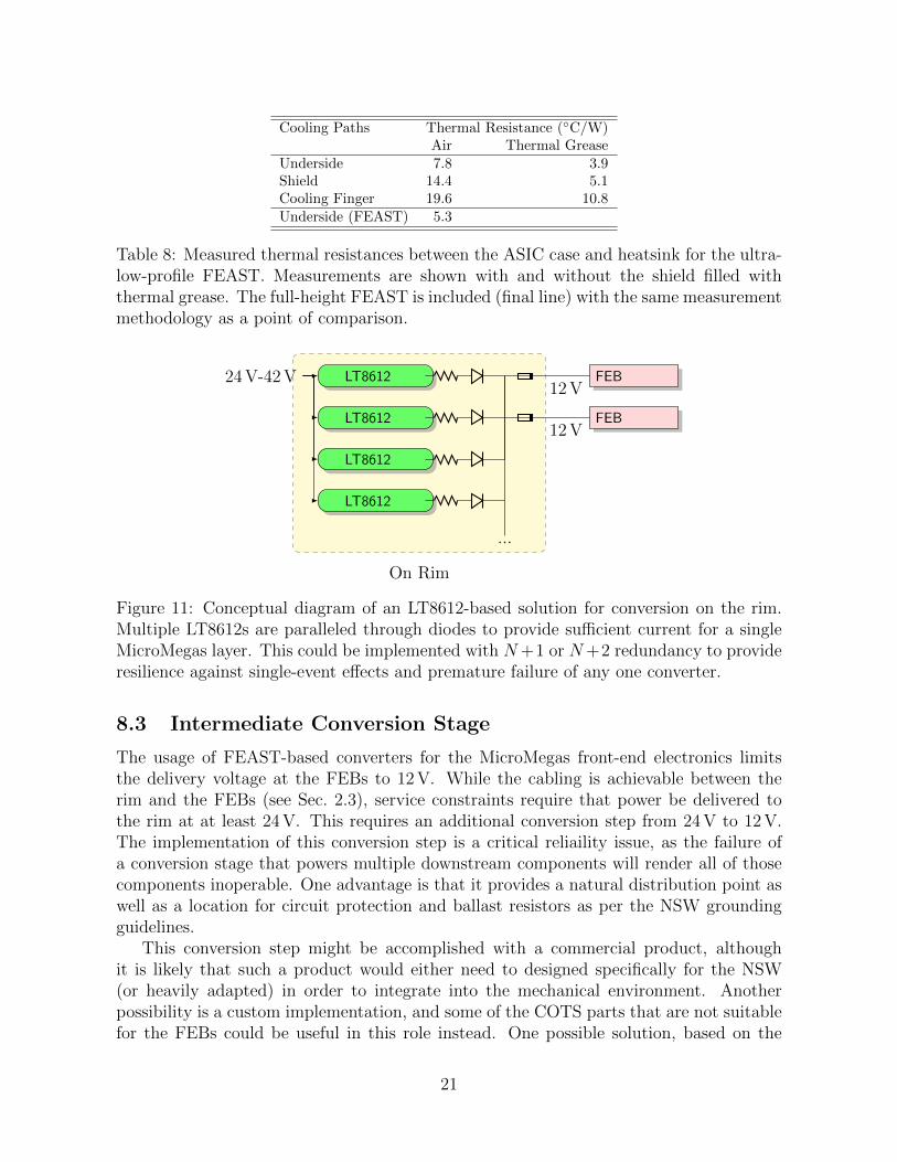
Cooling Paths Thermal Resistance (C/W)Air Thermal Grease
Underside 7.8 3.9Shield 14.4 5.1Cooling Finger 19.6 10.8Underside (FEAST) 5.3
Table 8: Measured thermal resistances between the ASIC case and heatsink for the ultra-low-profile FEAST. Measurements are shown with and without the shield filled withthermal grease. The full-height FEAST is included (final line) with the same measurementmethodology as a point of comparison.
24 V-42 V LT8612
LT8612
LT8612
LT8612
...
FEB
FEB
12 V
12 V
On Rim
Figure 11: Conceptual diagram of an LT8612-based solution for conversion on the rim.Multiple LT8612s are paralleled through diodes to provide sufficient current for a singleMicroMegas layer. This could be implemented with N+1 or N+2 redundancy to provideresilience against single-event effects and premature failure of any one converter.
8.3 Intermediate Conversion Stage
The usage of FEAST-based converters for the MicroMegas front-end electronics limitsthe delivery voltage at the FEBs to 12 V. While the cabling is achievable between therim and the FEBs (see Sec. 2.3), service constraints require that power be delivered tothe rim at at least 24 V. This requires an additional conversion step from 24 V to 12 V.The implementation of this conversion step is a critical reliaility issue, as the failure ofa conversion stage that powers multiple downstream components will render all of thosecomponents inoperable. One advantage is that it provides a natural distribution point aswell as a location for circuit protection and ballast resistors as per the NSW groundingguidelines.
This conversion step might be accomplished with a commercial product, althoughit is likely that such a product would either need to designed specifically for the NSW(or heavily adapted) in order to integrate into the mechanical environment. Anotherpossibility is a custom implementation, and some of the COTS parts that are not suitablefor the FEBs could be useful in this role instead. One possible solution, based on the
21
LT8612, is shown in Figure 11. The LT8612 can accept an input voltage of up to 42 Vand produce an output current of 6 A at any lower voltage. Paralleling several convertersusing diodes can provide N + 1 or N + 2 redundancy, thus protecting against SEE and/orpremature failure of any one converter. This would require N=4 if one supply handles asingle MicroMegas layer, or N=2 for one side of one layer.
Note also that this conversion step, whether commercial or custom, need not be locatedon the rim; it could conceivably be placed along the MM cooling channels in an unusedlocated to take advantage of the existing cooling system.
9 Status and recommendations
Of the buck converters that have been evaluated for use in the New Small Wheel, noCOTS option appears fully viable in the higher-radiation regions at low radii. Both theleading COTS candidates - the LT8612 and LTM4619 - display troubling single-eventeffects when exposed to protons. The LTM4619 is strongly affected by magnetic fieldlevels that would be present on the NSW rim. The LT8612 appears usable on the rim,e.g. as a conversion step to provide 10 V-12 V to electronics located in higher-radiationregions, particularly if measures are taken to mitigate the impact of single-event effects.
The FEAST, while not usable in it’s module form, does not suffer from radiationconcerns. Our recommendation is to integrate the FEAST ASIC(s) directly onto thefront-end boards. This produces the best electrical performance while minimizing therequired PCB area. With a magnetically-tolerant low-profile ferrite, the total height ofthis solution is 4 mm. This imposes minimal constraint on placement due to height.Cooling from either above or below is viable with this solution. Furthermore, the coolingchannel capacity is adequate for cables supplying 10 V from the rim without undue cableloss.
This solution necessitates an additional conversion step on the rim. As mentionedabove, the LT8612 appears suitable for this task. However, exploring the optimal meansof accomplishing this conversion step remains an open issue.
Three possibilities presently remain for voltage regulators. The space-qualified TexasInstruments TPS7H1101 is being explored as an option, however, its large size andpresently-unknown price may limit its application. One COTS regulators, the MaximMAX8556, appears sufficiently resilient but still requires evaluation for its susceptibilityto displacement damage. This is currently in progress. One final option is that voltageregulators may prove unnecessary - the conducted noise from the FEAST can be reducedto extremely low levels with only moderate passive filtering. This possibility would best betested by integrating a FEAST-only power solution into a demonstrator front-end boardand evaluating the effect.
In summary, the remaining open issues are:
1. Fully resolve the integration of the FEAST, along with noise and cooling issues, andproduce a reference design for board designers.
2. Qualify the MAX8556 or TPS7H1101, or validate the no-voltage-regulator options.
22

3. Understand the options for conversion on the rim, commercial vs. custom with theLT8612, and from where it would be procured.
23

Table 9: Measured inductance for a variety of COTS parts in several magnetic fieldstrengths.
Inductor Magnetic Field Tolerance
Manufacturer Part InductanceRated B=0 B=2kG B=4kG B=6.5kG
Power Inductors (Testing @ 1.8MHz)1 Coiltronics HCM0703-R47-R 0.47 .58 .54 .42 .152 Coiltronics HCM0703-1R0-R 1.00 .97 .88 .71 .363 Coiltronics HCM0703-4R7-R 4.70 5.15 4.57 3.52 1.65
4 Coilcraft XAL5030-601MEB 0.60 .69 .46 .40 .115 Coilcraft XAL4020-601MEB 0.60 .57 .43 .33 .126 Coilcraft XAL4020-102MEB 1.00 1.01 .65 .48 .197 Coilcraft XAL5030-222MEB 2.20 2.11 1.31 .73 .318 Coilcraft XAL5030-472MEB 4.70 5.57 3.07 1.61 .689 Coilcraft XAL4030-472MEB 4.70 4.44 2.59 1.71 .61
10 Vishay-Dale IHLP-2525CZERR47M01 0.47 .56 .42 .33 .1511 Vishay-Dale IHLP-2525CZ-01 1.00 1.07 .98 .84 .4912 Vishay-Dale IHLP-2525CZER4R7M01 4.70 3.75 3.41 2.75 1.24
13 Wurth 744 355 147 0.47 .42 .18 .16 .0914 Wurth 744 373 460 047 0.47 .59 .53 .45 .1415 Wurth 744 310 055 0.52 .60 .49 .43 .1216 Wurth 744 778 004 0.52 .57 .09 -17 Wurth 744 311 068 0.68 .72 .47 .39 .0918 Wurth 744 778 001 1.00 .99 .12 .11 .1019 Wurth 744 311 220 2.20 2.41 1.70 .72 .2420 Wurth 744 778 002 2.20 2.31 .28 .27 .2021 Wurth 744 373 460 33 3.30 3.27 2.90 2.32 1.0622 Wurth 744 355 137 0 3.70 3.35 1.41 .56 .4723 Wurth 744 373 240 47 4.70 4.97 4.50 3.33 1.9024 Wurth 744 778 005 4.70 4.04 .53 .48 -25 Wurth 744 311 220 6.50 6.55 3.35 1.08 -26 Wurth 744 311 650 6.50 6.63 3.13 .96 .5227 Wurth 744 373 461 00 10.00 10.30 10.10 8.56 6.5228 Wurth WE7447797470 4.70 4.32 .54 .52 .42
EMI Chokes (Testing @ 1MHz)29 Fair-Rite 2744065447 2.72 .09 .08 -30 Fair-Rite 2744045447 .88 .06 .05 -31 Fair-Rite 2752041447 .16 .04 .04 -32 Fair-Rite 2752045447 .40 .09 .09 -33 Fair-Rite 2744555567 6.15 .07 .06 -34 Fair-Rite 2744555577 10.46 .12 .10 -35 Fair-Rite 2773021447 3.49 .05 .05 -36 Fair-Rite 2773019447 1.80 .03 .03 -
37 Murata BLM21PG221SN1D 1.54 .05 - -
38 Coiltronics MPI2520R0-R47-R 0.47 .60 .50 .35 .18Continued on next page
24

Table 9 – continued from previous pageManufacturer Part Inductance
Rated B=0 B=2kG B=4kG B=6.5kG39 Coiltronics MPI2520R1-R47-R 0.47 .43 .34 .17 .11
40 Bourns SRR0603-100ML 10.00 9.71 1.48 1.33 1.19
41 Vishay-Dale ILHB0603ER600V .40 .02 .02 .0142 Vishay-Dale ILHB0603ER121V .91 .06 .05 .0443 Vishay-Dale ILC0603ERR27J 0.27 .39 .39 .40 .4044 Vishay-Dale IMC0603ER15NG01 0.01545 Vishay-Dale IMC0603ER22NG01 0.02246 Vishay-Dale IMC0603ER3N3S 0.003347 Vishay-Dale IMC0603ER15NG 0.015
48 Coilcraft 1206USB-172MLB 1.74 .09 .0649 Coilcraft 1206USB-371MLB .42 .07 .06 .0650 Coilcraft 1206USB-102MLB .51 .09 .06 .04
51 Wurth 782 633 620 .50 .04 .0252 Wurth 782 631 101 .23 .07 .06 .0553 Wurth 782 633 601 4.58 .14 .09 .08
54 Yuden BRC1608TR77M 0.77 .75 .30 .12 .12WE Inductor Testing MAPI and LHMI Families(Testing @ 1MHz)
55 Wurth 744 373 240 10 1 1.03 .95 .74 .4356 Wurth 744 373 340 10 1 .94 .87 .66 .5157 Wurth 744 373 460 10 1 1.05 .89 .59 .3558 Wurth 744 383 130 033 0.33 .52 .45 .37 .2659 Wurth 744 383 130 068 0.68 .76 .74 .59 .3760 Wurth 744 383 130 10 1 .90 .85 .69 .4861 Wurth 744 383 210 10 1 1.13 1.08 .89 .7962 Wurth 744 383 240 10 1 1.09 1.03 .63 .4263 Wurth 744 383 430 10 1 1.01 .96 .80 .52
References
[1] Gianluigi De Geronimo Personal Communication
[2] Michelis, S. et al, DC-DC converters in 0.35µm CMOS technology JINST 7 C01072
[3] Abbate, C. et al, Developments on DC/DC converters for the LHC experiment up-grades, JINST 9 C02017
[4] Lazzaroni, M.; Citterio, M.; Latorre, S.; Lanza, A.; Spiazzi, G., Point of Load forLHC experiments: Testing the behaviour in hostile environment, Instrumentation andMeasurement Technology Conference (I2MTC) Proceedings, 2014 IEEE International,pp.681-686, 12-15 May 2014
25

[5] Lazzaroni, M.; Citterio, M.; Latorre, S.; Lanza,A., High B Test of a commercial step-down Point of Load for LHC experiments, Measurement, Available online 20 October2014, ISSN 0263-2241
[6] Fuentes, C.; Allongue, B.; Blanchot, G.; Faccio, F.; Michelis, S.; Orlandi, S.; Pontt,J.; Rodriguez, J.; Kayal, M., Optimization of DC-DC Converters for Improved Elec-tromagnetic Compatibility With High Energy Physics Front-End Electronics, NuclearScience, IEEE Transactions on , vol.58, no.4, pp.2024,2031, Aug. 2011
[7] Fuentes, C., Optimization of the design of DC-DC converters for improving the elec-tromagnetic compatibility with the Front-End electronic for the super Large HadronCollider Trackers Ph.D. Dissertation, Universidad Tecnica Federico Santa Marıa
26