
A Synchrophasor-and-Active-Load-Based Oscillation Damping ... · A...
16
A Synchrophasor-and-Active-Load-Based Oscillation Damping Controller Hardware Prototype for the Icelandic Power System Guðrún Margrét Jónsdóttir, [email protected] Muhammad Shoaib Almas (supervisor), [email protected] Luigi Vanfretti (professor), [email protected] 22-24th March 2015 NASPI Work Group Meeting
Transcript of A Synchrophasor-and-Active-Load-Based Oscillation Damping ... · A...

A Synchrophasor-and-Active-Load-Based Oscillation Damping Controller Hardware Prototype for the Icelandic Power System
Guðrún Margrét Jónsdóttir, [email protected]
Muhammad Shoaib Almas (supervisor), [email protected]
Luigi Vanfretti (professor), [email protected]
22-24th March 2015NASPI Work Group Meeting

https://www.wikipedia.org/
Iceland
2www.telegraph.co.uk
www.icelandluxury.com
www.boredpanda.com
icelandintro.is
www.bluelagoon.com

Motivation
3
-> Heavily loaded and aging infrastructure
-> Poorly damped inter-area oscillatory modes.
Load disconnection
0.4 Hz oscillation
Line Trip
0.3 Hz oscillation
Icelandic Power System
Idea:Control the load of aluminium smelters.
3
Assumptions and limitations The study was limited to only one inter-area oscillatory mode at a time.
The Icelandic system, and most other power systems, have several modes that need to be considered.
The tests were carried out using the two-area four-machine Klein-Rogers-Kundur power system model.
Resembles the Icelandic network.
The aluminum smelter load were not modelled in detail.
Aluminum smelters are represented using three phase dynamic loads.
The load could be increased and decreased instantaneously.
Aluminum smelters load demand can be increased instantaneously, however, their power output needs to be modulated within equipment constraints.
4
• Determine the maximum and minimum.
• Determine whether to increase or decrease.
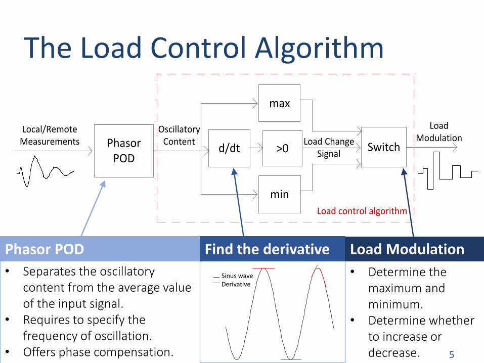
The Load Control Algorithm
d/dt
max
minLoad control algorithm
Load ModulationPhasor
POD
Local/Remote Measurements
Oscillatory Content Load Change
SignalSwitch>0
Sinus waveDerivative
Phasor POD
• Separates the oscillatory content from the average value of the input signal.
• Requires to specify the frequency of oscillation.
• Offers phase compensation.
Find the derivative Load Modulation
5
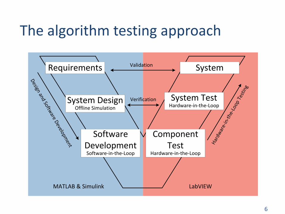
Requirements
System DesignOffline Simulation
Software DevelopmentSoftware-in-the-Loop
System
System TestHardware-in-the-Loop
Component Test
Hardware-in-the-Loop
Validation
Verification
Design and Softw
are Developm
ent Har
dwar
e-in
-the
-Loo
p Te
stin
g
MATLAB & Simulink LabVIEW
The algorithm testing approach
6
7
Hardware-in-the-LoopSoftware-in-the-Loop
1. Real-time execution of power system model.2. Send Voltage and Current signals to PMU.3. The PMU forwards the data to the PDC.4. S3DK unwraps the PDC stream to access raw measurements.5. Load control algorithm deployed on the NI-cRIO. 6. Send Load modulation signal back to the RTS.
Real-TimeSimulator
SEL-487 E PMU
Communication Network
(Managed Ethernet Switch)
PMU Stream
Phasor Data Concentrator (PDC)
Legend
HardwiredHardwired
PMU streamPMU stream
PDC streamPDC stream
Feedback SignalFeedback Signal
Bypass Amplifiers Connect to Low-level
Input on the PMU
Load Modulation
Two Area Kundur Test System simulated on the
Real-Time Simulator
1.
2.
3.
4.
5.
6.
G1
G2
Area 1
Local Loads
220 Km Parallel Transmission Lines
Power TransferArea 1 to Area 2
G3
G4
Local Loads
Area 2
Control Load in Area 2
d/dt <0
max
min Load control algorithm
Load Modulation
Phasor POD
Local/Remote Measurements
Oscillatory Content Load Change
SignalSwitch
To External controller
MATLAB/SimulinkSimPowerSystems
Model Design
OPAL-RT‘s eMEGASIM Real-Time Simulator
d/dt <0
max
min
Phasor POD
Switch
G1
G2
Area 1
G3
G4
Area 2
Control Load in Area 2
64 Analog Out
16 Analog In
Simulator Analog and Digital I/Os
OP 5251 (64 DO)
OP 5251 (64 DI)
1.
2. 3.
4.
5.
1. The power system model and the load controller are simulated on two separate cores on the RTS.
2. Load modulation signal from Load controller model in Simulink is configured to one of the DOs of the RTS.
3. Digital Output and Input are looped back.
4. Load modulation signal is received by one of the DIs of the RTS and configured to change the load.
5. Workstation with RT-Lab software for monitoring the RT simulation.
The power system model in MATLAB/SimulinkArea 2 in the power system model in MATLAB/Simulink
The load controlled in Area 2
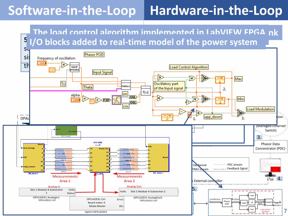
The load control algorithm implemented in MATLAB/SimulinkThe load control algorithm implemented in LabVIEW FPGA
Analog OutAnalog In
OP5142EX1 Ctrl
Board index: 0
Mode:Master
Error
IDs
OpCtrl OP5142EX1
Slot 1 Module B Subsection 1
Volts
Status
OP5142EX1 AnalogIn1'OP5142EX1 Ctrl'
Slot 2 Module A Subsection 2Volts
OP5142EX1 AnalogOut3'OP5142EX1 Ctrl'
Measurements Area 1
Measurements Area 2
I/O blocks added to real-time model of the power system
7
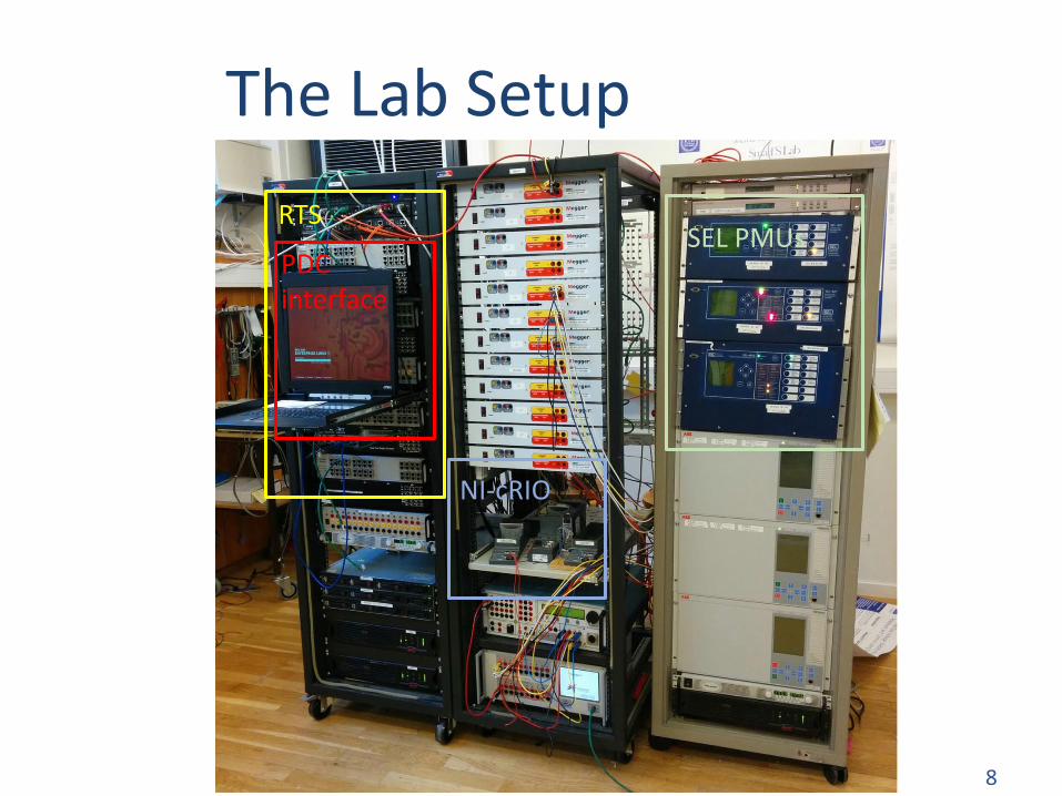
RTS
PDC interface
SEL PMUs
NI-cRIO
The Lab Setup
8
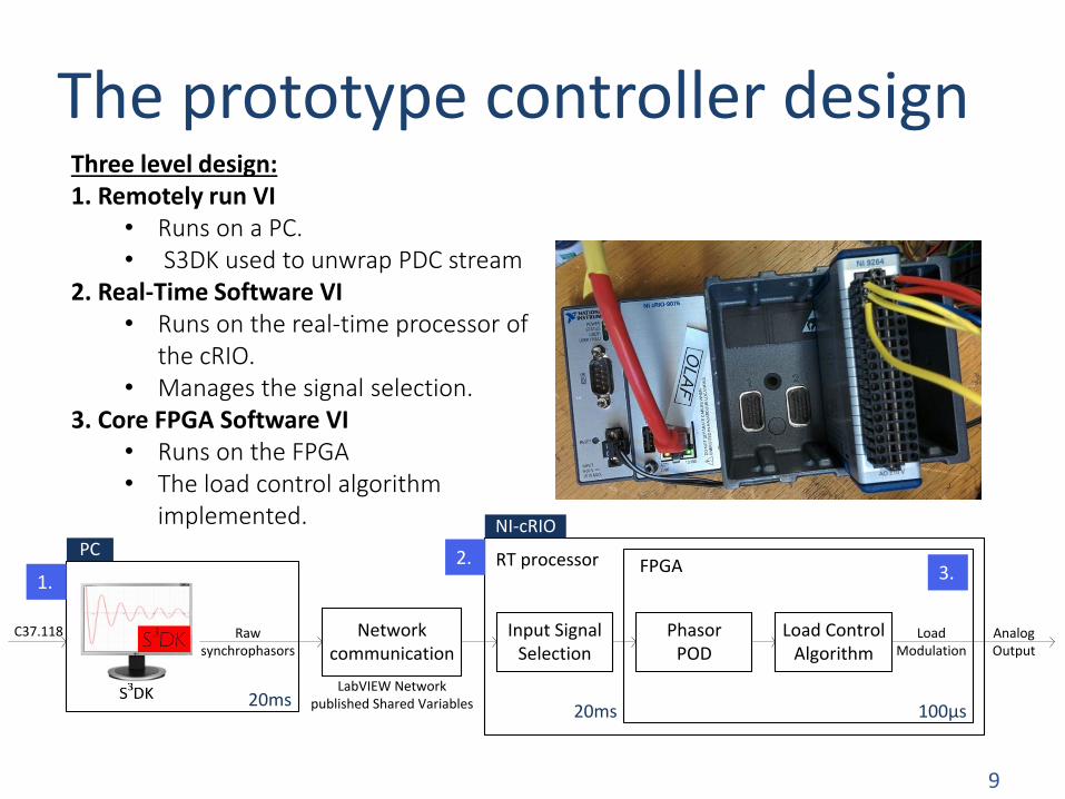
The prototype controller design
Network communication
Raw synchrophasors
LabVIEW Networkpublished Shared Variables
Input Signal Selection
PhasorPOD
Load ControlAlgorithm
NI-cRIOPC
RT processor FPGA
20ms 100µs20ms
LoadModulation
AnalogOutput
C37.118
Three level design:1. Remotely run VI
• Runs on a PC.• S3DK used to unwrap PDC stream
2. Real-Time Software VI• Runs on the real-time processor of
the cRIO.• Manages the signal selection.
3. Core FPGA Software VI• Runs on the FPGA • The load control algorithm
implemented.
1.2.
3.
9
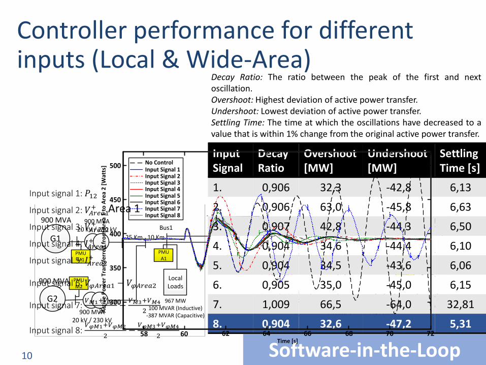
Controller performance for different inputs (Local & Wide-Area)
10
G1
G2
Area 1
Local Loads
900 MVA
900 MVA 900 MVA20 kV / 230 kV
25 Km 10 Km
900 MVA20 kV / 230 kV
967 MW100 MVAR (Inductive)
-387 MVAR (Capacitive)
220 Km Parallel Transmission Lines
Power TransferArea 1 to Area 2
10 Km 25 Km
900 MVA900 MVA20 kV / 230 kV
G4900 MVA
20 kV / 230 kV 900 MVA
Area 2
Bus1 Bus2
Local Loads
1767 MW100 MVAR (Inductive)
-537 MVAR (Capacitive)
Phasor POD
Load Control
Algorithm
Local/RemoteMeasurement
Oscillatory Content
Load Modulation
PMUM1
PMUM2
G3PMUM3
PMUM4
PMUMiddle
PMUA1
PMUA2
Input signal 1: 𝑃12
Input signal 2: 𝑉𝐴𝑟𝑒𝑎1+
Input signal 3: 𝑉𝐴𝑟𝑒𝑎2+
Input signal 4: 𝐼𝐴𝑟𝑒𝑎1+
Input signal 5: 𝐼𝐴𝑟𝑒𝑎2+
Input signal 6: 𝑉𝜑𝐴𝑟𝑒𝑎1 − 𝑉𝜑𝐴𝑟𝑒𝑎2
Input signal 7: 𝑉𝑀1+𝑉𝑀2
2−
𝑉𝑀3+𝑉𝑀4
2
Input signal 8: 𝑉𝜑𝑀1+𝑉𝜑𝑀2
2−
𝑉𝜑𝑀3+𝑉𝜑𝑀4
2
ΔVref G1
Input Signal
Decay Ratio
Overshoot[MW]
Undershoot [MW]
Settling Time [s]
1. 0,906 32,3 -42,8 6,13
2. 0,906 63,0 -45,8 6,63
3. 0,907 42,8 -44,3 6,50
4. 0,904 34,6 -44,4 6,10
5. 0,904 34,5 -43,6 6,06
6. 0,905 35,0 -45,0 6,15
7. 1,009 66,5 -64,0 32,81
8. 0,904 32,6 -47,2 5,31
Decay Ratio: The ratio between the peak of the first and nextoscillation.Overshoot: Highest deviation of active power transfer.Undershoot: Lowest deviation of active power transfer.Settling Time: The time at which the oscillations have decreased to avalue that is within 1% change from the original active power transfer.
Software-in-the-Loop58 60 62 64 66 68 70 72
300
350
400
450
500 No ControlInput Signal 1Input Signal 2Input Signal 3Input Signal 4Input Signal 5Input Signal 6Input Signal 7Input Signal 8
Act
ive
Po
we
r T
ran
sfe
rre
d f
rom
Are
a 1
to
Are
a 2
[W
att
s]
Time [s]
Input signal 1: 𝑃12
Input signal 2: 𝑉𝐴𝑟𝑒𝑎1+
Input signal 3: 𝑉𝐴𝑟𝑒𝑎2+
Input signal 4: 𝐼𝐴𝑟𝑒𝑎1+
Input signal 5: 𝐼𝐴𝑟𝑒𝑎2+
Input signal 6: 𝑉𝜑𝐴𝑟𝑒𝑎1 − 𝑉𝜑𝐴𝑟𝑒𝑎2
Input signal 7: 𝑉𝑀1+𝑉𝑀2
2−
𝑉𝑀3+𝑉𝑀4
2
Input signal 8: 𝑉𝜑𝑀1+𝑉𝜑𝑀2
2−
𝑉𝜑𝑀3+𝑉𝜑𝑀4
2
10
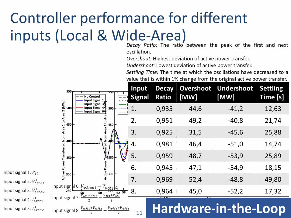
Controller performance for different inputs (Local & Wide-Area)
11
G1
G2
Area 1
Local Loads
900 MVA
900 MVA 900 MVA20 kV / 230 kV
25 Km 10 Km
900 MVA20 kV / 230 kV
967 MW100 MVAR (Inductive)
-387 MVAR (Capacitive)
220 Km Parallel Transmission Lines
Power TransferArea 1 to Area 2
10 Km 25 Km
900 MVA900 MVA20 kV / 230 kV
G4900 MVA
20 kV / 230 kV 900 MVA
Area 2
Bus1 Bus2
Local Loads
1767 MW100 MVAR (Inductive)
-537 MVAR (Capacitive)
Phasor POD
Load Control
Algorithm
Local/RemoteMeasurement
Oscillatory Content
Load Modulation
PMUM1
PMUM2
G3PMUM3
PMUM4
PMUMiddle
PMUA1
PMUA2
Input signal 1: 𝑃12
Input signal 2: 𝑉𝐴𝑟𝑒𝑎1+
Input signal 3: 𝑉𝐴𝑟𝑒𝑎2+
Input signal 4: 𝐼𝐴𝑟𝑒𝑎1+
Input signal 5: 𝐼𝐴𝑟𝑒𝑎2+
Input signal 6: 𝑉𝜑𝐴𝑟𝑒𝑎1 − 𝑉𝜑𝐴𝑟𝑒𝑎2
Input signal 7: 𝑉𝑀1+𝑉𝑀2
2−
𝑉𝑀3+𝑉𝑀4
2
Input signal 8: 𝑉𝜑𝑀1+𝑉𝜑𝑀2
2−
𝑉𝜑𝑀3+𝑉𝜑𝑀4
2
ΔVref G1
Hardware-in-the-Loop
Act
ive
Po
we
r T
ran
sfe
rre
d f
rom
Are
a 1
to
Are
a 2
[M
W]
Time [s]58 60 62 64 66 68 70 72 74 76
250
300
350
400
450
500
550
No ControlInput Signal 1Input Signal 3Input Signal 4Input Signal 6
Input Signal 2Input Signal 5Input Signal 7Input Signal 8
No Control
Act
ive
Po
we
r T
ran
sfe
rre
d f
rom
Are
a 1
to
Are
a 2
[M
W]
Time [s]58 60 62 64 66 68 70 72 74 76
250
300
350
400
450
500
550Input Signal
Decay Ratio
Overshoot[MW]
Undershoot [MW]
Settling Time [s]
1. 0,935 44,6 -41,2 12,63
2. 0,951 49,2 -40,8 21,74
3. 0,925 31,5 -45,6 25,88
4. 0,981 46,4 -51,0 14,74
5. 0,959 48,7 -53,9 25,89
6. 0,945 47,1 -54,9 18,15
7. 0,969 52,4 -48,8 49,80
8. 0,964 45,0 -52,2 17,32
Input signal 1: 𝑃12
Input signal 2: 𝑉𝐴𝑟𝑒𝑎1+
Input signal 3: 𝑉𝐴𝑟𝑒𝑎2+
Input signal 4: 𝐼𝐴𝑟𝑒𝑎1+
Input signal 5: 𝐼𝐴𝑟𝑒𝑎2+
Input signal 6: 𝑉𝜑𝐴𝑟𝑒𝑎1 − 𝑉𝜑𝐴𝑟𝑒𝑎2
Input signal 7: 𝑉𝑀1+𝑉𝑀2
2−
𝑉𝑀3+𝑉𝑀4
2
Input signal 8: 𝑉𝜑𝑀1+𝑉𝜑𝑀2
2−
𝑉𝜑𝑀3+𝑉𝜑𝑀4
2
Decay Ratio: The ratio between the peak of the first and nextoscillation.Overshoot: Highest deviation of active power transfer.Undershoot: Lowest deviation of active power transfer.Settling Time: The time at which the oscillations have decreased to avalue that is within 1% change from the original active power transfer.
11
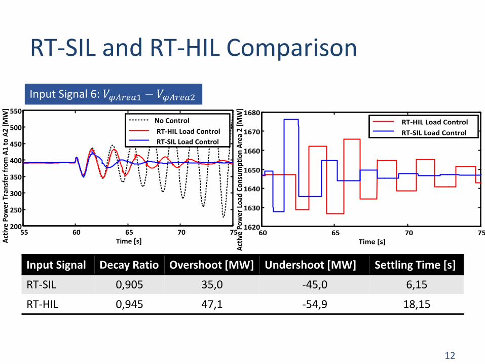
RT-SIL and RT-HIL Comparison
55 60 65 70 75200
250
300
350
400
450
500
550
Time [s]Act
ive
Po
wer
Tra
nsf
er f
rom
A1
to A
2 [M
W]
No Control
RT-HIL Load Control
RT-SIL Load Control
60 65 70 751620
1630
1640
1650
1660
1670
1680
Time [s]A
ctiv
e Po
wer
Loa
d Co
nsum
ptio
n A
rea
2 [M
W]
RT-HIL Load Control
RT-SIL Load Control
Input Signal 6: 𝑉𝜑𝐴𝑟𝑒𝑎1 − 𝑉𝜑𝐴𝑟𝑒𝑎2
Input Signal Decay Ratio Overshoot [MW] Undershoot [MW] Settling Time [s]
RT-SIL 0,905 35,0 -45,0 6,15
RT-HIL 0,945 47,1 -54,9 18,15
12

Further Analysis of Simulation ResultsMain factors contributing to difference in RT-HIL and RT-SIL simulation results:
D/A
Co
nversio
n
A/D
Co
nversio
nD
/A C
on
version
A/D Conversion
Real-TimeSimulator SEL-487 E PMU
PDC
PC
cRIORT
FPGA
TCP
TCP
TCP
1. 2. 3.
4.5.
6.
Digital signal
Analog signal
Model simulated in Real-Time
Divide by1.4*103
Divide by1.8*105
Voltage
Current
Inside Real-Time Simulator
Multiply by1000
Multiply by10
Inside PMU
Compute input signal
Inside cRIO
1. 2. 3.
4.
Divide by120
Multiply by3*106
1. Signal has to be within ±5𝑉.
2. Scaled up with pre-configured CT and VT turn ratio.
3. Signal has to be within ±10𝑉.
4. Analog input limit of simulator.
Load
Co
ntr
ol S
ign
al
Time [s] Time [s]60 65 70 75 80
-1
0
1
2x 10
7
61.4 61.6 61.8 62 62.2 62.41.211
1.212
1.213
1.214
1.215x 10
7
(a) (b)
• Latency
• Scaling
• NoiseNoise in the range of ±20 kW.
Note that the peak output is 121 MW.
Fixed delay: • RTS• PMU• NI-cRIO
Non-deterministic delay:• PDC• S3DK• The communication protocols
• Difference in implementation
Requirements
System DesignOffline Simulation
Software DevelopmentSoftware-in-the-Loop
System
System TestHardware-in-the-Loop
Component Test
Hardware-in-the-Loop
Validation
Verification
Design and Softw
are Developm
ent Har
dwar
e-in
-the
-Loo
p Te
stin
g
MATLAB & Simulink LabVIEW
The same programming language and development platform can not be used for SIL and HIL.
13
Summary
A load control algorithm was designed for damping of inter-area oscillations.
The algorithm utilizes synchrophasor measurements (local and/or remote) as an input signal.
Tested in RT-SIL and RT-HIL for eight different input signals (synchrophasors).
Voltage angle difference, current and active power performed the best.
HIL performance is affected by scaling, noise, latencies and difference in implementation.
14
Future Work Create an equivalent model of the Icelandic power system in Simulink
SimPowerSystems and prepare for real-time simulation on OPAL RT eMEGASIM real-time simulator.
Verify the model using PMU measurements from the system.
Test the load controllers damping performance in the system.
Enhancement of the load control algorithm.
Design and testing multiple oscillatory modes and ambient load variations.
15
Thank you!
16