


Langages
Pages
Légal

Direct Measurement ofDensity-of-States EffectiveMass and Scattering Parameterin Transparent conductingOxides Using Second-OrderTransport Phenomena
March 2000 � NREL/CP-520-27747
D.L. Young and T.J. CouttsNational Renewable Energy Laboratory
V.I. KaydanovColorado School of Mines: Golden, Colorado
W.P. MulliganSunpower Inc.: Sunnyvale, California
Presented at the American Vacuum Society 46th
International SymposiumSeattle, WashingtonOctober 24-29, 1999
National Renewable Energy Laboratory1617 Cole BoulevardGolden, Colorado 80401-3393NREL is a U.S. Department of Energy LaboratoryOperated by Midwest Research Institute •••• Battelle •••• Bechtel
Contract No. DE-AC36-99-GO10337
NOTICEThe submitted manuscript has been offered by an employee of the Midwest Research Institute (MRI), acontractor of the US Government under Contract No. DE-AC36-99GO10337. Accordingly, the USGovernment and MRI retain a nonexclusive royalty-free license to publish or reproduce the publishedform of this contribution, or allow others to do so, for US Government purposes.
This report was prepared as an account of work sponsored by an agency of the United Statesgovernment. Neither the United States government nor any agency thereof, nor any of their employees,makes any warranty, express or implied, or assumes any legal liability or responsibility for the accuracy,completeness, or usefulness of any information, apparatus, product, or process disclosed, or representsthat its use would not infringe privately owned rights. Reference herein to any specific commercialproduct, process, or service by trade name, trademark, manufacturer, or otherwise does not necessarilyconstitute or imply its endorsement, recommendation, or favoring by the United States government or anyagency thereof. The views and opinions of authors expressed herein do not necessarily state or reflectthose of the United States government or any agency thereof.
Available electronically at http://www.doe.gov/bridge
Available for a processing fee to U.S. Department of Energyand its contractors, in paper, from:
U.S. Department of EnergyOffice of Scientific and Technical InformationP.O. Box 62Oak Ridge, TN 37831-0062phone: 865.576.8401fax: 865.576.5728email: [email protected]
Available for sale to the public, in paper, from:U.S. Department of CommerceNational Technical Information Service5285 Port Royal RoadSpringfield, VA 22161phone: 800.553.6847fax: 703.605.6900email: [email protected] ordering: http://www.ntis.gov/ordering.htm
Printed on paper containing at least 50% wastepaper, including 20% postconsumer waste
Paper presented at the American Vacuum Society 46thInternational Symposium in Seattle, WA.October 24-29, 1999
Abstract Number: 1045Program Number: TF-WeA10
Session Title: Transparent Conductive Oxides
Direct Measurement of Density-of-States Effective Mass and Scattering Parameter inTransparent Conducting Oxides Using Second-Order Transport Phenomena
D.L. Young, T.J. Coutts, National Renewable Energy Laboratory, Golden, COV.I. Kaydanov, Colorado School of Mines, Golden, CO.W.P. Mulligan, Sunpower Inc. Sunnyvale, CA.
Abstract:
The Boltzmann transport equation can be solved to give analytical solutions to the resistivity, Hall, Seebeck, and
Nernst coefficients. These solutions may be solved simultaneously to give the density-of-states (DOS) effective
mass ( md* ), the Fermi energy relative to either the conduction or valence band, and a scattering parameter that is
related to a relaxation time and the Fermi energy. The Nernst coefficient is essential for determining the scattering
parameter and, thereby, the effective scattering mechanism(s). We constructed equipment to measure these four
transport coefficients simultaneously over a temperature range of 30-350 K for thin, semiconducting films deposited
on insulating substrates. We measured these coefficients for rf magnetron-sputtered zinc oxide, both doped and
undoped, with aluminum with carrier concentrations in the range of 1x10¹⁹ - 5x1020 cm-3. The ( md* ) was not constant
over this carrier concentration range: varying from 0.3 to 0.48 me, leading us to conclude that zinc oxide has a non-
parabolic conduction band. Conductivity effective mass values for zinc oxide matched our md* values, revealing a
single valley, nearly spherical, constant energy surface for zinc oxide. The measured scattering parameter changed
from close to zero to 1.5 as the carrier concentrations increased. The scattering parameter, Seebeck, and mobility vs.
temperature data support neutral impurity scattering in the undoped material and ionized impurity scattering in the
Al-doped ZnO. The transport theory also allows an extrapolation for an md* value at the bottom of the conduction
band, which was found to be 0.27 me.
2
Introduction
Transparent conductive oxide (TCO), thin-film semiconductors are used in many large-volume and
technically significant applications,1 yet they remain some of the least-understood materials, in part due to their
relatively poor transport properties. TCO films represent a compromise between optical transmittance, bounded by
absorbance at the optical band gap and reflectance at the plasma frequency, and electrical conductivity. As noted by
Coutts et al.,2 this compromise must pivot about maximizing the mobility. For highly degenerate, metal-like TCO
films, mobility may be defined by the Drude theory, µ = qτ m* , where m* is the conductivity effective mass and τ
is the time between carrier-scattering elastic collisions, known as the relaxation time. Obviously, either a long
relaxation time or a small m* will increase the mobility, but either quantity represents a formidable task to measure;
the former is very difficult. Cyclotron and de Haas van Alphen resonance techniques, the traditional methods for
probing the Fermi surface via the effective mass, are only applicable for high-mobility materials because of the
constraint that the product µB >> 1 so that electrons complete at least one orbit before they are scattered. With
typical magnetic fields in the laboratory being on the order of one Tesla, the mobility must be in the tens of
thousands cm2/V-s. TCOs, with their relatively small mobilities (µ < 300 cm2/V-s) and short relaxation times (~10-15
s), do not meet the µB >> 1 requirement and are thus unsuitable for these measurement techniques. Effective mass
values for polycrystalline, thin-film TCOs are usually inferred from optical modeling (plasma frequency, or
transmission, reflection data) or assumed to be equal to single-crystal bulk values.
In addition to the need for a direct measure of m* in TCOs and other polycrystalline thin films,
understanding the mechanism for scattering of carriers in films is of great importance for improving transport
properties. To better understand the band structure and the dominant scattering mechanisms, a novel measurement
technique, based on transport phenomena, has been applied to TCO thin-films. Transport-phenomena coefficient
measurements � resistivity, Hall, Seebeck, and Nernst (sometimes referred to as Nernst-Ettingshausen) � on thin-
film TCO samples were used with solutions to the Boltzmann transport equation to make direct measurements of the
DOS effective mass, md* , and an energy-dependent scattering parameter, s. We have constructed equipment to enable
these measurements for films grown on electrically insulating substrates. We have applied this technique to TCO
thin-film samples and have made, to our knowledge, the first direct measurements of md* and s on films of cadmium
3
stannate, zinc oxide, tin oxide, and cadmium oxide. In this paper, we will discuss transport theory, our transport
coefficient equipment, and data obtained from our zinc oxide study.
Theory
Transport, or motion of charge carriers in a material, is described by Boltzmann�s transport equation, which
relates changes in the carrier distribution (occupied energy states) to forces that drive the carriers to a non-
equilibrium state. The carriers (electrons for n-type materials) in a degenerate material in equilibrium are described
by the Fermi-Dirac distribution function, � fo(
��
k ,��
r ) . When external driving forces from temperature gradients or
electric and magnetic fields are imposed on a material, the carriers are driven to higher energy (excited) states. The
redistribution of occupied energy levels from the equilibrium configuration may be described by a non-equilibrium
distribution function, ��
f (��
k ,��
r ) . Carriers in excited states will return to their equilibrium distribution after collision,
scattering events between other charge carriers or imperfections in the material.3 Transport by electric and thermal
current densities in a material are described by
��
��
J = q4π 3
��v f (��
k ,��r )dk� Amps/m2 �
��
Q = 14π 3 (E − EF )
��v f (��
k , ��r ,)dk� Watts/m2, [1]
where �� ��
v is the carrier velocity. To solve these integrals, �
f (��
k ,��
r ) must be determined by solving the steady-state
Boltzmann transport equation,4
��
∂f∂t
� � � �
� � ≈
q�
(��E +
��v ×
��B ) ⋅
��∇ k f (
��k ,��r ) +
��v ⋅
��∇ r f (
��k ,��r ) ,
which relates the rate-of-change of the non-equilibrium function to driving forces acting on the non-equilibrium
energy distribution of carriers. Obviously, this is a very difficult equation to solve because it requires knowledge of
occupation and transition probabilities between excited and equilibrium states. Traditionally, a relaxation time
approximation has been made to allow analytical solutions. This approximation assumes a mean time between
collisions, when carriers are forced from an excited to an equilibrium distribution or vice versa�known as the
relaxation time, τ. The change in the distribution function can be approximated by
∂f∂t
� � � �
� � ≈
f0 − fτ
� � � �
� � 1/sec.
The relaxation time between collisions is not a function of direction of the carrier motion, but is a function of energy
and possibly temperature.3 The frequency of elastic collisions, τ-1(E), depends on the density-of-states function,
4
g(E), and the square of the matrix element of the scattering transition from one energy state to a final state of the
same energy, w(E). For parabolic energy bands, g( E ) ∝ E1/ 2 , while w(E) is a power function of energy
w( E ) ∝ E− s ∝ ( k 2 )−s . Thus, τ−1( E ) = w( E )g( E ) = E − sE1/ 2 = E1/ 2− s , which is often written
τ ∝ E s−1/ 2 ∝ E ′ s with s' = s - 1/2. For the parabolic band model, s' has been identified for several scattering
mechanisms that are:
Acoustic Phonon scattering �> s' = -1/2, s = 0
Neutral Impurity scattering �> s' = 0, s = 1/2
Ionized Impurity scattering �> s' = 3/2 s = 2
In the non-parabolic energy-band case, the energy of the carriers can be described by the function
��
�2k 2
2md0*
= γ ( E ) = E +E 2
E1+
E 3
E2+ ... [2]
where E1 and E2 are constants, which preserves the same transition matrix element dependence on k 2 as in the
parabolic case. The non-parabolic density-of-states function, gN .P .( E ) ∝γ 1/ 2 dγ
dE� � � �
� , leads to
τN .P.
−1 = w( E )N .P.g( E )N .P. ∝γ − sγ 1/ 2 dγdE
� � � �
� ,
and finally,
τ ∝ γ s−1/ 2 dγ
dE� � � �
�
−1
∝γ s' dγdE
� � � �
�
−1
. [3]
Clearly, the s' values for different scattering mechanisms in the non-parabolic case are the same as in the parabolic
case.
Many texts3-6 outline the solution of Boltzmann�s equation for �
f (��
k ,��
r ) using the relaxation time
approximation and further solve equations [1] for electric and thermal current densities. In general, equations [1]
have the following form,3
Jα =q
4π 3 vα2
� τGα (E)∂f0
∂Edk and Qα =
14π 3 (E − EF )vα
2� τGα (E)
∂f0
∂Edk , [4]
where Gα (E) is a function of temperature gradients and electric and magnetic forces, and α represents different
crystallographic directions. Equations [4] may be related to the phenomenological equations for carrier transport,
5
Jα = σαβEβ −θαβdTdxβ
and Qα = χαβ Eβ − ξαβdTdxβ
, [5]
to identify specific transport coefficients. In equations [5], Eβ is an electric field, dT dxβ is a temperature gradient
across a sample, andσαβ ,θαβ , χαβ ,ξαβ are transport tensors that depend on the orientation and strength of a magnetic
field.7 To match experimental setups, temperature gradients and electric fields are placed in the x, y plane, whereas
magnetic fields are parallel to the z-axis. This arrangement leads to analytical solutions for conductivity, Hall,
Seebeck, and Nernst coefficients. Integral equations for n-type material coefficients are
σ =q2nm *
τ conductivity, RH =−1nq
τ 2
τ 2 Hall,
α =−1qT
τEτ
− EF
�
� �
�
� � Seebeck, Q =
−µn
qTτ 2Eτ 2 −
τ 2 τEτ 3
�
� �
�
� � Nernst,
where τ mEn =τ m En( )Eg(E)
∂f0
∂EdE
0
∞
�
Eg(E) ∂f0
∂EdE
0
∞
� and g(E) is a density-of-states function.
Kolodziejczak et al.7 first solved equations [6] for materials with ellipsoidal energy surfaces. Later, Kaydanov8 also
solved the equations using the energy function described by equation [2]. When γ ( E ) = E , the (in general) non-
parabolic energy bands become parabolic. γ ( E ) , then, describes the state of non-parabolicity for the energy bands
in a material. Analytic expressions for equations [6] are solved using the method of Bethe-Sommerfeld9 to
approximate the Fermi integrals. Keeping only lowest-order, non-vanishing terms, the conductivity and Hall
coefficients require only first-order terms in the Sommerfeld expansion, whereas the Seebeck and Nernst coefficients
require retention of second-order terms to first-order in temperature. The results for the Seebeck and Nernst
coefficients for low magnetic fields µB << 1 and isotropic materials of high degeneracy are
α0 =
23
α∞ s + 1 − λ{ } Seebeck coefficient [7]
Q0 = µ 2
3α ∞ s −
12
− λ� � �
� � �
Nernst coefficient, [8]
[6]
6
where λ = 2γ dγ
dε� � � �
�
−2d 2γdε 2
, s is the scattering parameter, and µ is the mobility. The term�� α∞ =
k02T
q�2π3n
� � � �
�
2 3
md* is
the Seebeck coefficient under high magnetic field (µB >> 1) and md
* = md0* dγ
dε is the energy-dependent DOS
effective mass, with md 0* representing the DOS effective mass at the conduction-band minimum. Notice that the
second term within the braces for equations [7] and [8], λ, depends on the energy bands of the material and vanishes
for parabolic-band materials when γ ( E ) is constant. Kolodziejczak et al.10 noticed that the high field Seebeck
effect could be used to probe the energy band of a material without knowledge of the scattering mechanism.
Dubrovskaya et al.11 investigated single-crystal PbTe in this manner. Unfortunately, this technique is not applicable
for TCOs, again, because of their low mobilities and the µB >> 1 requirement for high field measurements.
Zhitinskaya et al.12 were the first to recognize that equations [7] and [8] could be combined to give equations
for the effective density-of-states mass at the Fermi level,
�� md
* =3nπ
� � � �
�
23 q�2
kB2T
α −Qµ
� � � �
� , [9]
and s, the scattering parameter,
s =32
Qµ
� �
� �
α − Qµ
� �
� �
+12
+ λ . [10]
Substituting into [9] µ = RH σ and n ≈ 1 RHq , where RH is the Hall coefficient, we obtain
��
md* =
3RH qπ
�
� �
�
� �
23 q� 2
kB2T
α −Q
RH σ�
� �
�
� � , [11]
which illustrates that the DOS effective mass may be experimentally determined by measuring the conductivity, Hall,
Seebeck, and Nernst coefficients of a sample. This technique has been coined the method of four coefficients8 and
was originally applied to p-type PbTe single crystals.13 Our group has applied the method of four coefficients to
thin-film TCO samples, using a specially designed instrument to measure the four coefficients on the same sample.
7
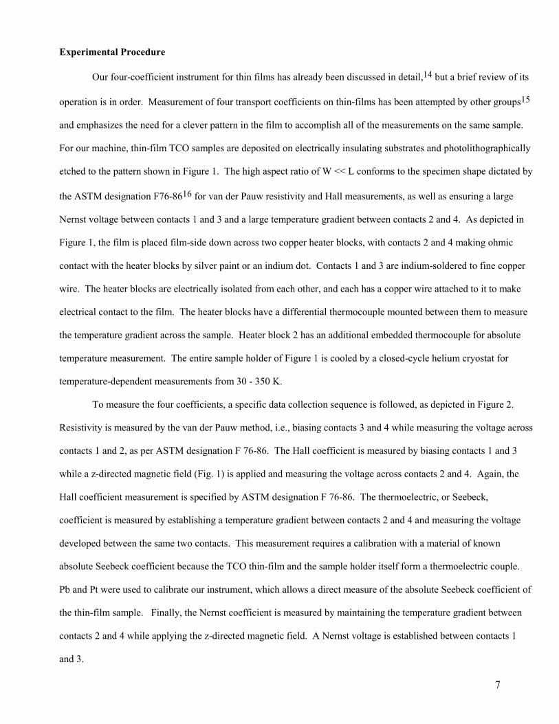
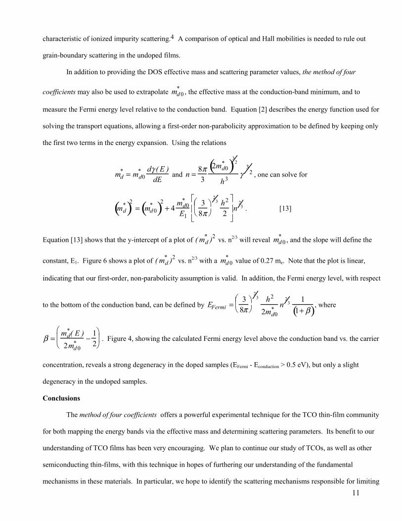
Experimental Procedure
Our four-coefficient instrument for thin films has already been discussed in detail,14 but a brief review of its
operation is in order. Measurement of four transport coefficients on thin-films has been attempted by other groups15
and emphasizes the need for a clever pattern in the film to accomplish all of the measurements on the same sample.
For our machine, thin-film TCO samples are deposited on electrically insulating substrates and photolithographically
etched to the pattern shown in Figure 1. The high aspect ratio of W << L conforms to the specimen shape dictated by
the ASTM designation F76-8616 for van der Pauw resistivity and Hall measurements, as well as ensuring a large
Nernst voltage between contacts 1 and 3 and a large temperature gradient between contacts 2 and 4. As depicted in
Figure 1, the film is placed film-side down across two copper heater blocks, with contacts 2 and 4 making ohmic
contact with the heater blocks by silver paint or an indium dot. Contacts 1 and 3 are indium-soldered to fine copper
wire. The heater blocks are electrically isolated from each other, and each has a copper wire attached to it to make
electrical contact to the film. The heater blocks have a differential thermocouple mounted between them to measure
the temperature gradient across the sample. Heater block 2 has an additional embedded thermocouple for absolute
temperature measurement. The entire sample holder of Figure 1 is cooled by a closed-cycle helium cryostat for
temperature-dependent measurements from 30 - 350 K.
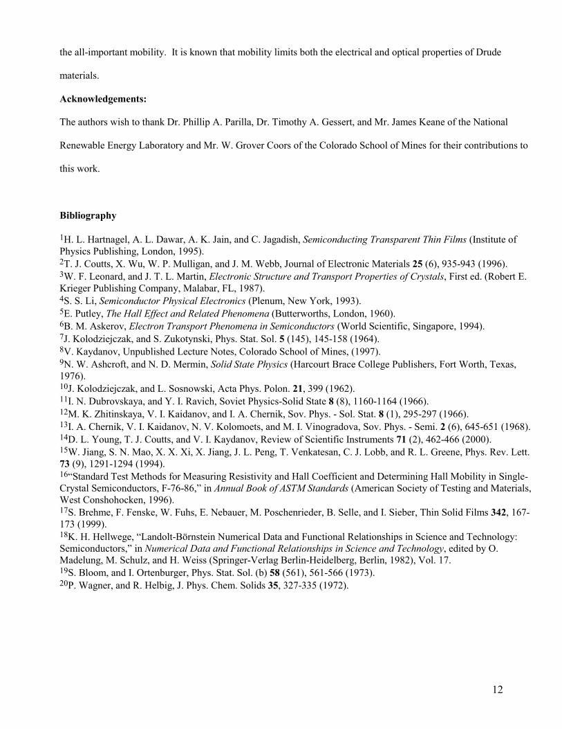
To measure the four coefficients, a specific data collection sequence is followed, as depicted in Figure 2.
Resistivity is measured by the van der Pauw method, i.e., biasing contacts 3 and 4 while measuring the voltage across
contacts 1 and 2, as per ASTM designation F 76-86. The Hall coefficient is measured by biasing contacts 1 and 3
while a z-directed magnetic field (Fig. 1) is applied and measuring the voltage across contacts 2 and 4. Again, the
Hall coefficient measurement is specified by ASTM designation F 76-86. The thermoelectric, or Seebeck,
coefficient is measured by establishing a temperature gradient between contacts 2 and 4 and measuring the voltage
developed between the same two contacts. This measurement requires a calibration with a material of known
absolute Seebeck coefficient because the TCO thin-film and the sample holder itself form a thermoelectric couple.
Pb and Pt were used to calibrate our instrument, which allows a direct measure of the absolute Seebeck coefficient of
the thin-film sample. Finally, the Nernst coefficient is measured by maintaining the temperature gradient between
contacts 2 and 4 while applying the z-directed magnetic field. A Nernst voltage is established between contacts 1
and 3.
8
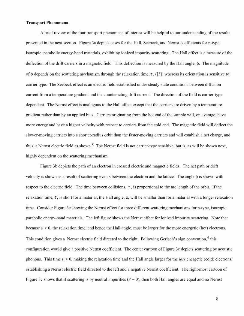
Transport Phenomena
A brief review of the four transport phenomena of interest will be helpful to our understanding of the results
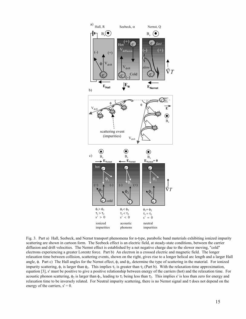
presented in the next section. Figure 3a depicts cases for the Hall, Seebeck, and Nernst coefficients for n-type,
isotropic, parabolic energy-band materials, exhibiting ionized impurity scattering. The Hall effect is a measure of the
deflection of the drift carriers in a magnetic field. This deflection is measured by the Hall angle, φ. The magnitude
of φ depends on the scattering mechanism through the relaxation time,τ , ([3]) whereas its orientation is sensitive to
carrier type. The Seebeck effect is an electric field established under steady-state conditions between diffusion
current from a temperature gradient and the counteracting drift current. The direction of the field is carrier-type
dependent. The Nernst effect is analogous to the Hall effect except that the carriers are driven by a temperature
gradient rather than by an applied bias. Carriers originating from the hot end of the sample will, on average, have
more energy and have a higher velocity with respect to carriers from the cold end. The magnetic field will deflect the
slower-moving carriers into a shorter-radius orbit than the faster-moving carriers and will establish a net charge, and
thus, a Nernst electric field as shown.5 The Nernst field is not carrier-type sensitive, but is, as will be shown next,
highly dependent on the scattering mechanism.
Figure 3b depicts the path of an electron in crossed electric and magnetic fields. The net path or drift
velocity is shown as a result of scattering events between the electron and the lattice. The angle φ is shown with
respect to the electric field. The time between collisions, τ , is proportional to the arc length of the orbit. If the
relaxation time,τ , is short for a material, the Hall angle, φ, will be smaller than for a material with a longer relaxation
time. Consider Figure 3c showing the Nernst effect for three different scattering mechanisms for n-type, isotropic,
parabolic energy-band materials. The left figure shows the Nernst effect for ionized impurity scattering. Note that
because s' > 0, the relaxation time, and hence the Hall angle, must be larger for the more energetic (hot) electrons.
This condition gives a Nernst electric field directed to the right. Following Gerlach�s sign convention,5 this
configuration would give a positive Nernst coefficient. The center cartoon of Figure 3c depicts scattering by acoustic
phonons. This time s' < 0, making the relaxation time and the Hall angle larger for the less energetic (cold) electrons,
establishing a Nernst electric field directed to the left and a negative Nernst coefficient. The right-most cartoon of
Figure 3c shows that if scattering is by neutral impurities (s' = 0), then both Hall angles are equal and no Nernst
9
electric field is established. The Nernst effect gives a clear signal for the type of scattering occurring in a parabolic
band material by changing the sign of the Nernst voltage.
It is interesting to note that if the γ (ε ) function in [7] and [8] is not constant (non-parabolic energy bands),
then the last term in [7] and [8] could become large enough to change the sign of the Seebeck and Nernst
coefficients. This condition was first observed in n-type InSb,10 and it has appeared in our work with CdO,[Coutts,
2000 #96] where the effective mass changes by a factor of three over an order of magnitude increase in carrier
concentration. Because the degree of non-parabolicity of the energy bands can affect the sign of the Nernst effect,
one must be careful in drawing conclusions about the scattering mechanism based solely on the sign of the Nernst
coefficient, until the band shape has been mapped with a variety of carrier concentration samples. The last term in
equations [7] and [8] may be shown to equal
2γ dγdε
� � � �
�
−2d 2γdε 2
E F
= 3n
md*
dmd*
dn = 3dLn[md
* ]dLn[ n] = λ , [12]
which allows direct measurement of the degree of non-parabolicity of a material once md* is known (via equation
[11]) for a number of samples of different carrier concentrations.
Results
Our group has applied the method of four coefficients to several TCO thin-films grown under a variety of
conditions. In this paper, we will present our preliminary findings on rf magnetron sputtered, undoped zinc oxide,
and zinc oxide doped with aluminum thin-films. Prepared samples were photolithographically patterned to the shape
shown in Figure 1 with film thickness measured by profilometry. The four relevant transport phenomena coefficients
(conductivity, Hall, Seebeck, and Nernst) were measured by the method and by the instrument described above, and
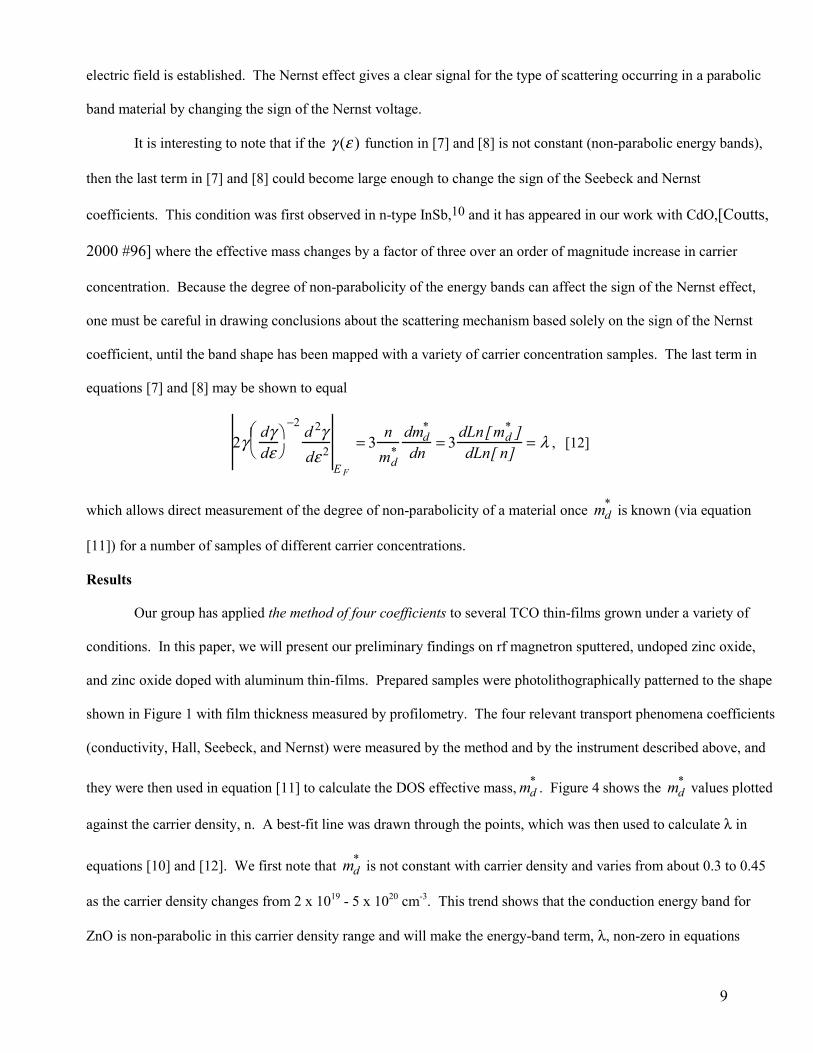
they were then used in equation [11] to calculate the DOS effective mass, md* . Figure 4 shows the md
* values plotted
against the carrier density, n. A best-fit line was drawn through the points, which was then used to calculate λ in
equations [10] and [12]. We first note that md* is not constant with carrier density and varies from about 0.3 to 0.45
as the carrier density changes from 2 x 10¹⁹ - 5 x 1020 cm-3. This trend shows that the conduction energy band for
ZnO is non-parabolic in this carrier density range and will make the energy-band term, λ, non-zero in equations
10
[7],[8], and [10]. In addition to our md* values for ZnO plotted in Figure 4, conductivity effective-mass values are
plotted, as well. These values were taken from the literature17,18 on plasma frequency-calculated conductivity
effective masses. Note that the conductivity and DOS effective mass are in good agreement with each other, but that
the error bars on the DOS effective mass are much smaller. Recalling that the relationship between the two effective-
mass values is given by md* = N
23( m1
* m2* m3
* )1
3 , we conclude that N, the number of ellipsoids of revolution, must
be one and that the conductivity effective-mass values ( m1* m2
* m3* ) for different crystallographic directions must be
approximately equal. This being the case, we may conclude that ZnO has a single-valley minimum in the conduction
energy band and that the constant energy surface must be spherical to within experimental uncertainty. The single-
valley minimum of ZnO is predicted by theory,19 but the uncertainty in the plasma frequency data makes it difficult
to be certain of the spherical nature of the energy surface. We note that ZnO is hexagonal and that our films have a
(200) orientation. Anisotrophy in the effective mass is not found in the literature, nor is it observed in the mobility
above 100 K.20
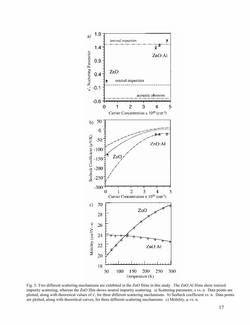
With md* known as a function of n, we solve for λ to determine the degree to which the band shape affects
the scattering parameter, s, in equation [10]. Figure 5a shows the calculated scattering parameter values from
equation [10] for our ZnO samples, along with the predicted trends in the scattering parameter for three different
scattering mechanisms. For the ZnO:Al samples, the measured scattering parameter matches well with the trend
expected for ionized impurities. This result is expected for these films, where aluminum is added to dope the films n-
type by contributing an electron to the conduction band, leaving behind an ionized aluminum atom. For the undoped
material, the scattering parameter is found to lie most closely with the neutral impurity trend. To further support our
claim that neutral and ionized impurity scattering are the main scattering mechanisms in ZnO and ZnO:Al,
respectively, Figure 5b shows our Seebeck measurements plotted against expected Seebeck values for three
scattering mechanisms. Again, ionized and neutral impurity scattering are the apparent mechanisms. Mobility vs.
temperature data for both a ZnO and ZnO:Al film are shown in Figure 5c. The undoped ZnO film shows a clear
positive dependence of mobility on temperature, indicative of neutral impurities. As the temperature decreases, the
number of neutral impurity centers will increase, decreasing the relaxation time between collisions, and thus
decreasing the mobility.6 For the doped material, the mobility is seen to be almost constant with temperature,
11
characteristic of ionized impurity scattering.4 A comparison of optical and Hall mobilities is needed to rule out
grain-boundary scattering in the undoped films.
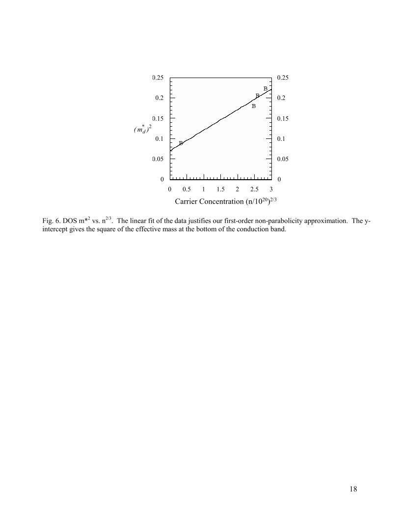
In addition to providing the DOS effective mass and scattering parameter values, the method of four
coefficients may also be used to extrapolate md 0* , the effective mass at the conduction-band minimum, and to
measure the Fermi energy level relative to the conduction band. Equation [2] describes the energy function used for
solving the transport equations, allowing a first-order non-parabolicity approximation to be defined by keeping only
the first two terms in the energy expansion. Using the relations
md
* = md0* dγ ( E )
dE and n =
8π3
2md0*( )3
2
h3γ
32 , one can solve for
md
*( )2 = md 0*( )2
+ 4md0
*
E1
38π
� � � �
�
23 h2
2
�
� �
� n
23 . [13]
Equation [13] shows that the y-intercept of a plot of ( md* )2 vs. n2/3 will reveal md 0
* , and the slope will define the
constant, E1. Figure 6 shows a plot of ( md* )2 vs. n2/3 with a md 0
* value of 0.27 me. Note that the plot is linear,
indicating that our first-order, non-parabolicity assumption is valid. In addition, the Fermi energy level, with respect
to the bottom of the conduction band, can be defined by EFermi =
38π
� � � �
�
23 h2
2md0*
n2
3 11+ β( ), where
β =
md*( E )
2md 0* −
12
�
� �
�
� � . Figure 4, showing the calculated Fermi energy level above the conduction band vs. the carrier
concentration, reveals a strong degeneracy in the doped samples (EFermi - Econduction > 0.5 eV), but only a slight
degeneracy in the undoped samples.
Conclusions
The method of four coefficients offers a powerful experimental technique for the TCO thin-film community
for both mapping the energy bands via the effective mass and determining scattering parameters. Its benefit to our
understanding of TCO films has been very encouraging. We plan to continue our study of TCOs, as well as other
semiconducting thin-films, with this technique in hopes of furthering our understanding of the fundamental
mechanisms in these materials. In particular, we hope to identify the scattering mechanisms responsible for limiting
12
the all-important mobility. It is known that mobility limits both the electrical and optical properties of Drude
materials.
Acknowledgements:
The authors wish to thank Dr. Phillip A. Parilla, Dr. Timothy A. Gessert, and Mr. James Keane of the National
Renewable Energy Laboratory and Mr. W. Grover Coors of the Colorado School of Mines for their contributions to
this work.
Bibliography
1H. L. Hartnagel, A. L. Dawar, A. K. Jain, and C. Jagadish, Semiconducting Transparent Thin Films (Institute ofPhysics Publishing, London, 1995).2T. J. Coutts, X. Wu, W. P. Mulligan, and J. M. Webb, Journal of Electronic Materials 25 (6), 935-943 (1996).3W. F. Leonard, and J. T. L. Martin, Electronic Structure and Transport Properties of Crystals, First ed. (Robert E.Krieger Publishing Company, Malabar, FL, 1987).4S. S. Li, Semiconductor Physical Electronics (Plenum, New York, 1993).5E. Putley, The Hall Effect and Related Phenomena (Butterworths, London, 1960).6B. M. Askerov, Electron Transport Phenomena in Semiconductors (World Scientific, Singapore, 1994).7J. Kolodziejczak, and S. Zukotynski, Phys. Stat. Sol. 5 (145), 145-158 (1964).8V. Kaydanov, Unpublished Lecture Notes, Colorado School of Mines, (1997).9N. W. Ashcroft, and N. D. Mermin, Solid State Physics (Harcourt Brace College Publishers, Fort Worth, Texas,1976).10J. Kolodziejczak, and L. Sosnowski, Acta Phys. Polon. 21, 399 (1962).11I. N. Dubrovskaya, and Y. I. Ravich, Soviet Physics-Solid State 8 (8), 1160-1164 (1966).12M. K. Zhitinskaya, V. I. Kaidanov, and I. A. Chernik, Sov. Phys. - Sol. Stat. 8 (1), 295-297 (1966).13I. A. Chernik, V. I. Kaidanov, N. V. Kolomoets, and M. I. Vinogradova, Sov. Phys. - Semi. 2 (6), 645-651 (1968).14D. L. Young, T. J. Coutts, and V. I. Kaydanov, Review of Scientific Instruments 71 (2), 462-466 (2000).15W. Jiang, S. N. Mao, X. X. Xi, X. Jiang, J. L. Peng, T. Venkatesan, C. J. Lobb, and R. L. Greene, Phys. Rev. Lett.73 (9), 1291-1294 (1994).16�Standard Test Methods for Measuring Resistivity and Hall Coefficient and Determining Hall Mobility in Single-Crystal Semiconductors, F-76-86,� in Annual Book of ASTM Standards (American Society of Testing and Materials,West Conshohocken, 1996).17S. Brehme, F. Fenske, W. Fuhs, E. Nebauer, M. Poschenrieder, B. Selle, and I. Sieber, Thin Solid Films 342, 167-173 (1999).18K. H. Hellwege, �Landolt-Börnstein Numerical Data and Functional Relationships in Science and Technology:Semiconductors,� in Numerical Data and Functional Relationships in Science and Technology, edited by O.Madelung, M. Schulz, and H. Weiss (Springer-Verlag Berlin-Heidelberg, Berlin, 1982), Vol. 17.19S. Bloom, and I. Ortenburger, Phys. Stat. Sol. (b) 58 (561), 561-566 (1973).20P. Wagner, and R. Helbig, J. Phys. Chem. Solids 35, 327-335 (1972).
13
B
A
CD
12
3 4
heater block #1
Cu spade connectors
OFHC-Cu
z
x
y
B
heater
block #2
substrate
L =
16.0
a = 0.2
b =1.0
W = 3.0
2 film 4
3
1
Fig. 1. Photolithographically etched thin-film sample on electrically insulating substrate placed film-side downacross copper heater blocks. Lengths are in mm. Wires A and C provide electrical contact to the sample, anddifferential thermocouple, B, and thermocouple, D, provide temperature information.
14
V
conductivity (van der Pauw) Hall effect
Seebeck effect Nernst effect
VV�� ��
∇ T
VBz
Bz
1
23
4
Fig. 2. Measurement configurations for collecting conductivity, Hall, Seebeck, and Nernst coefficients on a single,thin-film sample. Note the temperature gradient for the Seebeck and Nernst measurements and the applied magneticfield for the Hall and Nernst measurements.
15
Bz
Hall, R Seebeck, α Nernst, Q
Eαααα
Vdiffusion
Vdrift
Cold
Hot
(-)
(+)
e-
e-
slow
fast
(-) (+)
ENernst
e-
e-�� ��
∇ T
EHall
Vdriftφ
(-) (+)
Bz
e-
scattering event (impurities)
E
Bz
Vdrift
φ φ
Vdrift
e-
ENernst
φ1
φ2
(+) (-)φ1
φ2
(+)(-)
ENernst
φ1
φ2
ENernst= 0
φ1> φ2τ1 > τ2s� > 0
φ1< φ2τ1 < τ2s� < 0
φ1= φ2τ1 = τ2s� = 0
ionized impurities
acoustic phonons
neutralimpurities
hot
cold
Bz Bz Bz
�� ��
∇ T
a)
b)
c)
e-e-e-
e-e-e-
Fig. 3. Part a) Hall, Seebeck, and Nernst transport phenomena for n-type, parabolic band materials exhibiting ionized impurityscattering are shown in cartoon form. The Seebeck effect is an electric field, at steady-state conditions, between the carrierdiffusion and drift velocities. The Nernst effect is established by a net negative charge due to the slower moving, "cold"electrons experiencing a greater Lorentz force. Part b) An electron in a crossed electric and magnetic field. The longerrelaxation time between collision, scattering events, shown on the right, gives rise to a longer helical arc length and a larger Hallangle, φ. Part c) The Hall angles for the Nernst effect, φ1 and φ2, determine the type of scattering in the material. For ionizedimpurity scattering, φ1 is larger than φ2. This implies τ1 is greater than τ2 (Part b). With the relaxation-time approximation,equation [3], s' must be positive to give a positive relationship between energy of the carriers (hot) and the relaxation time. Foracoustic phonon scattering, φ2 is larger than φ1, leading to τ1 being less than τ2. This implies s' is less than zero for energy andrelaxation time to be inversely related. For Neutral impurity scattering, there is no Nernst signal and τ does not depend on theenergy of the carriers, s' = 0.
16
Fig. 4. Density-of-states (DOS) effective mass, Fermi energy level with respect to the conduction band, and plasmafrequency - conductivity effective mass, mc, versus carrier concentration for ZnO and ZnO:Al.
17
Fig. 5. Two different scattering mechanisms are exhibited in the ZnO films in this study. The ZnO:Al films show ionizedimpurity scattering, whereas the ZnO film shows neutral impurity scattering. a) Scattering parameter, s vs. n. Data points areplotted, along with theoretical values of s', for three different scattering mechanisms. b) Seebeck coefficient vs. n. Data pointsare plotted, along with theoretical curves, for three different scattering mechanisms. c) Mobility, µ vs. n.
18
( md* )2
Carrier Concentration (n/1020)2/3
B
BB
B
0
0.05
0.1
0.15
0.2
0.25
0
0.05
0.1
0.15
0.2
0.25
0 0.5 1 1.5 2 2.5 3
Fig. 6. DOS m*2 vs. n2/3. The linear fit of the data justifies our first-order non-parabolicity approximation. The y-intercept gives the square of the effective mass at the bottom of the conduction band.
REPORT DOCUMENTATION PAGE Form ApprovedOMB NO. 0704-0188
Public reporting burden for this collection of information is estimated to average 1 hour per response, including the time for reviewing instructions, searching existingdata sources, gathering and maintaining the data needed, and completing and reviewing the collection of information. Send comments regarding this burdenestimate or any other aspect of this collection of information, including suggestions for reducing this burden, to Washington Headquarters Services, Directorate forInformation Operations and Reports, 1215 Jefferson Davis Highway, Suite 1204, Arlington, VA 22202-4302, and to the Office of Management and Budget, PaperworkReduction Project (0704-0188), Washington, DC 20503.
1. AGENCY USE ONLY (Leave blank) 2. REPORT DATEMarch 2000
3. REPORT TYPE AND DATES COVEREDconference paper
4. TITLE AND SUBTITLEDirect Measurement of Density-of-States Effective Mass and Scattering Parameter in TransparentConducting Oxides Using Second-Order Transport Phenomena6. AUTHOR(S)D.L. Young, T.J. Coutts, V.I. Kaydanov, and W.P. Mulligan
5. FUNDING NUMBERS
CTA: WW215201
7. PERFORMING ORGANIZATION NAME(S) AND ADDRESS(ES) 8. PERFORMING ORGANIZATIONREPORT NUMBER
9. SPONSORING/MONITORING AGENCY NAME(S) AND ADDRESS(ES)National Renewable Energy Laboratory1617 Cole Blvd.Golden, CO 80401-3393
10. SPONSORING/MONITORINGAGENCY REPORT NUMBER
CP-520-27747
11. SUPPLEMENTARY NOTES
12a. DISTRIBUTION/AVAILABILITY STATEMENTNational Technical Information ServiceU.S. Department of Commerce5285 Port Royal RoadSpringfield, VA 22161
12b. DISTRIBUTION CODE
13. ABSTRACT (Maximum 200 words)The Boltzmann transport equation can be solved to give analytical solutions to the resistivity, Hall, Seebeck, and Nernst coefficients. These solutions may be solved simultaneously to give the density-of-states (DOS) effective mass ( *
dm ), the Fermi energy relative to eitherthe conduction or valence band, and a scattering parameter that is related to a relaxation time and the Fermi energy. The Nernstcoefficient is essential for determining the scattering parameter and, thereby, the effective scattering mechanism(s). We constructedequipment to measure these four transport coefficients simultaneously over a temperature range of 30-350 K for thin, semiconductingfilms deposited on insulating substrates. We measured these coefficients for rf magnetron-sputtered zinc oxide, both doped and undoped,
with aluminum with carrier concentrations in the range of 1x10¹⁹ - 5x1020 cm-3. The ( md* ) was not constant over this carrier concentration
range: varying from 0.3 to 0.48 me, leading us to conclude that zinc oxide has a non-parabolic conduction band. Conductivity effective
mass values for zinc oxide matched our md* values, revealing a single valley, nearly spherical, constant energy surface for zinc oxide.
The measured scattering parameter changed from close to zero to 1.5 as the carrier concentrations increased. The scattering parameter,Seebeck, and mobility vs. temperature data support neutral impurity scattering in the undoped material and ionized impurity scattering in
the Al-doped ZnO. The transport theory also allows an extrapolation for an md* value at the bottom of the conduction band, which was
found to be 0.27 me.15. NUMBER OF PAGES 14. SUBJECT TERMS
photovoltaics ; transparent conducting oxides ; second-order transport phenomena ; density ofstates ; effective mass ; scattering parameters 16. PRICE CODE
17. SECURITY CLASSIFICATIONOF REPORTUnclassified
18. SECURITYCLASSIFICATIONOF THIS PAGEUnclassified
19. SECURITY CLASSIFICATIONOF ABSTRACTUnclassified
20. LIMITATION OF ABSTRACT
UL
NSN 7540-01-280-5500 Standard Form 298 (Rev. 2-89)Prescribed by ANSI Std. Z39-18
298-102
Top Related