
Zhen LI RECONFIGURABLE COMPUTING …RESUME FRANCAIS 1. Introduction A l'ère de l'explosion des...
188
N° d’ordre : 2015-01 Année : 2015 THESE délivré par L’ECOLE CENTRALE DE LYON Spécialité : Electronique, micro et nano-électronique, optique et laser Présentée et soutenue publiquement par Zhen LI Préparé à l’Institut des Nanotechnologies de Lyon (INL), UMR CNRS 5270 RECONFIGURABLE COMPUTING ARCHITECTURE EXPLORATION USING SILICON PHOTONICS TECHNOLOGY Ecole Doctoral E.E.A « Electronique, Electrotechnique, Automatique » de Université de Lyon Sera soutenue le 28 janvier 2015 devant la Commission d’Examen Jury : M.Peter Bienstman Associate Professeur, Ghent University Rapporteur M.Lionel Torres Professeur, Univ.de Montpellier 2 Rapporteur M.Yannick Dumeige HDR, Univ.de Rennes 1 Examinateur M.Jacques-Olivier Klein Professeur, Université Paris-Sud XI Examinateur M.Sébastien Le Beux Maitre de conférence, ECL Examinateur Mme.Christelle Monat Maitre de conférence, ECL Examinateur M.Xavier Letartre Directeur de recherche, CNRS Examinateur M.Ian O'Connor Professeur, ECL Directeur de thèse
Transcript of Zhen LI RECONFIGURABLE COMPUTING …RESUME FRANCAIS 1. Introduction A l'ère de l'explosion des...

N° d’ordre : 2015-01 Année : 2015
THESE délivré par
L’ECOLE CENTRALE DE LYON
Spécialité : Electronique, micro et nano-électronique, optique et laser
Présentée et soutenue publiquement par
Zhen LI
Préparé à l’Institut des Nanotechnologies de Lyon (INL), UMR CNRS 5270
RECONFIGURABLE COMPUTING ARCHITECTURE EXPLORATION USING SILICON PHOTONICS
TECHNOLOGY
Ecole Doctoral E.E.A « Electronique, Electrotechnique, Automatique » de Université de Lyon
Sera soutenue le 28 janvier 2015 devant la Commission d’Examen Jury : M.Peter Bienstman Associate Professeur, Ghent University Rapporteur M.Lionel Torres Professeur, Univ.de Montpellier 2 Rapporteur M.Yannick Dumeige HDR, Univ.de Rennes 1 Examinateur M.Jacques-Olivier Klein Professeur, Université Paris-Sud XI Examinateur M.Sébastien Le Beux Maitre de conférence, ECL Examinateur Mme.Christelle Monat Maitre de conférence, ECL Examinateur M.Xavier Letartre Directeur de recherche, CNRS Examinateur M.Ian O'Connor Professeur, ECL Directeur de thèse


i
REMERCIEMENTS
Tout d’abord, je tiens à remercier Peter Bienstman et Lionel Torres pour avoir joué le
role essentiel de rapporteurs de cette thèse, en lisant avec sérieux et indulgence ce manuscrite
« double-disciplinaire ». Peter et Lionel a aussi contribué grandement non seulement à
l’amélioration de l’architecture je proposé, et encore à reconsidérer ce travail sous un autre
horizon. Je joins à ces remerciements Jacques-Olivier Klein et Yannick Dumeige pour avoir
ajouté des visions différentes à la variété des compétences de mon jury et aussi pour leurs
remarques, questions et conseils lors de ma présentation.
Les quatres personnes restant du jury ont contribué plus intensément à la réussite de
cette thèse, mon directeur de thèse Ian O’Connor, avec Sébastien Le Beux, Christelle Monat
et Xavier Letartre. Je tiens à exprimer ma profonde gratitude envers cette équipe
d’encadrement « fantastique » et « croisé le monde du système et du photonique », pour
m’avoir encadré, accompagné, conseillé et soutenu tout au long de ma thèse, pour leur aides
scientifiques, organisationnelles et énormément encouragements à défendre mes idées et
suivre le chemin je choisie, pour l’ensemble de nos échanges stimulants, de nos débats
agreables et passionants ainsi que pour ces nombreuses relecteurs de ce manuscrite.
Je voudrais remercier Guy Hollinger (directeur de l’INL), Catherine Bru-Chevallier
(directrice INL) et Christian Seassal (directeur adjoint INL, résponsable site-ECL) pour
m’avoir accueillie au sein de l’INL et m’avoir permis d’effectuer cette thèse dans ses murs.
Bien sûr, Xavier a joué un rôle essentiel qui est un peu comme « le roi physique »
dans ces traveaux de thèse. Combien de fois j’ai pu apprécier de discuter avec toi des
problèmes épineux et mes questions à la fois « informé » et « inprécisé », et l’ésprit prolifique
de sortir un solution élégant et satisfaite (plus qu’un compromis) pour des choses compliqués.
Souvent je me sens plutot comme jouer un petit jeu de raisonnement avec toi, avec les échos
« et alors » « et alors » « mais c’est bien sur » ou « on sent fou», on a trouvé finalment c’était
tout simple !… J’espère vraiment que je me montrerai aussi l’ésprit que toi dans ma carrière
de recherche de futur.
Egalement, Christelle est aussi joué un rôle comme « mère optique » dans mes
traveaux. Toujours vivant, jamais à dire « oui » facilement sans une réflexion profondu pour

ii
tous ce que je t’ai parlé et proposé, tu es toujours curieuse et passionné à apprendre les
nouveaux (plus que du côte physique, mais aussi du système), à décourir des petits choses
intéréssantes, à tenir les détails au cœur et pu faire le lien entre eux quand t’a besoin (par
exemple, pour me montrer les choses bizzares ou inraisonnables qui sont dans un coin caché
de ma thèse). Pour ces moments, le mieux je peux faire est de te dire « je ne sais pas, et je vais
le bien vérifier après ». Mais plus qu’une perfectionniste et parfois « exigente » en science, tu
es aussi très attentive et tolérante, je ne sais plus combien de fois je suis ému que tu tiens sur
ma position à considérer et/ou à montré un autre angle sur mes idées et mes traveaux. Tu es le
premier exemple du chercheur accompli qui me vienne à l’esprit.
Egalement, Sébastien prends le rôle comme « boss système ». C’est vraiment difficile
à croire que tu as des imaginations si riches et tu as pu inspirer des belles idées chaque fois
qu’on échange et discute. J’ai encore bien du mal à réaliser comment tu parviens d’avoir le
grande vue en même temps n’oublier pas tous les petites détails, parfois je ne sais pas
comment te faire plaisir quand tu m’a dit « c’est pas claire ». Mais ce qui est précieuse pour
moi, c’est tu m’as parlé souvent la difficulté sur ce sujet multi-disciplinaire qui est entre le
système et physique (la communication, la compromis), surtout quand on n’étais pas content
sur les résultats, ta tolérence et personnalité fait toi comme « mon frère ».
Et finalement j’ai eu la chance d’avoir Ian, le meilleur directeur de la thèse, cette thèse
n’aurait pas pu voir le jour sans l’implication de toi. Je n’a pas pu de trouver un mot ou une
phrase pour merci ton support, tes encouragements, tes idées, tes temps, ta
compherension…tu es le « père » de ma vie de la science.
Je tiens aussi à mentioner le plaisir que j’ai eu à travailler au sein de l’équipe
conception et l’équipe nanophotonique et j’en remercie ici tous les membres. Merci également
auxadministrateurs systèmes (Laurent Carrel et Rapheal Lopez) et aux secrétaires (Sylvie,
Patricia), qui font un travail formidable pour le labo.
Je passe ensuite une dédicace spéciale à tous les jeunes que j’ai eu plaisir de cotôyer
durant ces quelques années à INL, à savoir Felipe Frantz, Barakat Jean-Baptiste, Zhu Nanhao,
Feng Zhengfu, Yang Zhugeng, Sui Ning, Zhang Taiping, Meng Xianqing, Liu Huanhuan, Yin
Shi, Liu Qiang, Ding He, Li Hui, Guan Xin, Shi Liu… J’ai aussi voulu remercier ceux qui
sont déjà repartis qui m’a partagé des moments inoubliables dans la vie à Ecully, Tianli
Huang, Yu Zhang, Meng Jie, … Merci égalment à tous mes amis qui, bien que souvent à

iii
distance, m’ont soutenu au cours de cette aventure : Tang Qingshan, Ning Baozhu, Bing
jingyi, Shi Peiluo, Wang Weijia…
Enfin, je souhaiterais remercier l’ensemble de ma famille pour m’avoir soutenu
au cours de ma thèse, mon père, ma copine et mes frères et mes sœurs. Et merci maman
au ciel, tu m’appris heureux, courage, dignité, je sens ta presence chaque jours.
« Pour ma maman au ciel,
Le paradis est sous tes pieds »

iv
v
RESUME
Les progrès dans la fabrication des systèmes de calcul reconfigurables de type « Field
Programmable Gate Arrays » (FPGA) s’appuient sur la technologie CMOS, ce qui engendre
une consommation des puces élevée. Des nouveaux paradigmes de calcul sont désormais
nécessaires pour remplacer les architectures de calcul traditionnel ayant une faible
performance et une haute consommation énergétique. En particulier, optique intégré pourrait
offrir des solutions intéressantes. Beaucoup de travail sont déjà adressées à l’utilisation
d’interconnexion optique pour relaxer les contraintes intrinsèques d’interconnexion
électronique. Dans ce contexte, nous proposons une nouvelle architecture de calcul
reconfigurable optique, la « optical lookup table » (OLUT), qui est une implémentation
optique de la lookup table (LUT). Elle améliore significativement la latence et la
consommation énergétique par rapport aux architectures de calcul d’optique actuelles tel que
RDL (« reconfigurable directed logic »), en utilisant le spectre de la lumière au travers de la
technologie WDM. Nous proposons une méthodologie de conception multi-niveaux
permettant l'explorer l’espace de conception et ainsi de réduire la consommation énergétique
tout en garantissant une fiabilité élevée des calculs (BER~10-18). Les résultats indiquent que
l’OLUT permet une consommation inférieure à 100fJ/opération logique, ce qui répondait en
partie aux besoins d’un FPGA tout-optique à l’avenir.

vi

vii
ABSTRACT
Advances in the design of high performance silicon chips for reconfigurable
computing, i.e. Field Programmable Gate Arrays (FPGAs), rely on CMOS technology and are
essentially limited by energy dissipation. New design paradigms are mandatory to replace
traditional, slow and power consuming, electronic computing architectures. Integrated optics,
in particular, could offer attractive solutions. Many related works already addressed the use of
optical on-chip interconnects to help overcome the technology limitations of electrical
interconnects. Integrated silicon photonics also has the potential for realizing high
performance computing architectures. In this context, we present an energy-efficient on-chip
reconfigurable photonic logic architecture, the so-called OLUT, which is an optical core
implementation of a lookup table. It offers significant improvement in latency and power
consumption with respect to optical directed logic architectures, through allowing the use of
wavelength division multiplexing (WDM) for computation parallelism. We proposed a multi-
level modeling approach based on the design space exploration that elucidates the optical
device characteristics needed to produce a computing architecture with high computation
reliability (BER~10-18) and low energy dissipation. Analytical results demonstrate the
potential of the resulting OLUT implementation to reach <100 fJ/bit per logic operation,
which may meet future demands for on-chip optical FPGAs.

viii
ix
RESUME FRANCAIS
1. Introduction
A l'ère de l'explosion des données, les systèmes de calcul sont un facteur clé pour
l’innovation des technologies de l'informatique et de la communication. En raison des besoins
sans-cesse croissantes en puissance de calcul, en rentabilité économique, et en efficacité
énergétique, les méthodes traditionnelles reposant sur une évolution incrémentale des
architectures de calcul ne suffisent plus ; des nouveaux paradigmes de calcul s’appuyant sur
de nouvelles technologies sont désormais nécessaires pour relever les défis énergétiques et de
performance.
ITRS (the International Technology Roadmap for Semiconductors) prédit que les
interconnexions électriques ne seront plus capables de supporter les échanges de données
ultrarapides dans les systèmes de calcul parallèle (e.g. système sur puce multiprocesseurs,
MPSoC), du fait de leurs faibles efficacités énergétiques et de leur faible bande passante.
L’optique intégrée sur puce fait partie des alternatives susceptibles de répondre aux besoins
en vitesse et en faible consommation des circuits intégrés (IC), cela en leur conférerant
davantage de fiabilité. En effet, selon [12] and [17], l’optique permet d’augmenter la bande
passante, de diminuer la latence et la consommation associée aux interconnexions. De plus, la
compatibilité de l’optique avec les procédés de fabrication traditionnels CMOS permet de
réduire fortement les couts de développements et de fabrication tout en garantissant un accès
aux techniques d'assemblage hautement intégrés.
Au-delà de l'utilisation de la photonique sur silicium pour la réalisation
d’interconnexions dans les architectures multi-processeurs, cette technologie peut également
être exploitée pour effectuer des calculs en tout-optique, bénéficiant ainsi des avantages
intrinsèques de la lumière, cad une bande passante élevée et une consommation énergétique
plus faible. Cependant, il est illusoire de penser que l'optique peut directement concurrencer
l'électronique dans les système de calcul en raison de son immaturité technologique, qui induit
naturellement des problèmes d'intégration, de fiabilité et de coût de fabrication. Une première
étape consiste donc à rendre l'optique utile dans des fonctions de niche, cela afin d’améliorer
les futurs systèmes de calcul. Cela nécessite de repenser et d’imaginer de nouvelles
x
architectures de calcul adaptés à l’optique et capable de tirer profit de ses bonne propriété [3].
Une feuille de route permettant de développer des architectures de calcul exploitant l’optique
peuvent être résumés ainsi: a) le calcul doit rester autant que possible dans le domaine optique
afin de limiter l'utilisation d'interfaces électro-optiques couteuse; b) le spectre de la lumière
doit être utilisés via le multiplexage en longueurs d’onde (« wavelength division
multiplexing », WDM) afin de représenter et traiter l'information de manière efficace et
compacte; c) l’architecture optique doit être reconfigurable pour permettre plus de flexibilité
et d’adaptabilité selon les applications traitées; d) l'optique doit permettre d’améliorer
l'efficacité énergétique des systèmes de calcul.
Dans cette thèse, nous proposons une nouvelle architecture de calcul optique, la
« Optical LookUp table » (OLUT), qui est une implémentation optique de la Lookup table
(LUT). Les progrès dans la fabrication des systèmes de calcul reconfigurables de type « field
programmable gate arrays » (FPGA) s’appuient sur la technologie CMOS, ce qui engendre
une consommation des puces élevée. Dans la mesure où la technologie CMOS approche de
ses limites fondamentales, l’approche classique visant à densifier les ressources de calculs au
sein des FPGAs mènera à des puissances surfaciques élevées qui ne pourront être réduite que
par une limitation de l’activité. Continuer à réduire le nombre de pJ/bits avec chaque
génération de technologie n’est donc plus possible. La photonique sur silicium, quant à elle, a
le potentiel pour franchir cette barrière énergétique et augmenter le rapport
performances/puissance des FPGAs, permettant ainsi de réduire l'écart entre FPGAs et ASICs.
L'architecture OLUT proposée permet d’accélérer les calculs en utilisant le spectre de
la lumière au travers de la technologie WDM. Elle améliore significativement la latence et la
consommation énergétique par rapport aux architectures de calcul d’optique actuelles tel que
RDL (« reconfigurable directed logic »). Nous proposons une méthodologie de conception
multi-niveaux permettant l'explorer l’espace de conception et ainsi de réduite la
consommation énergétique tout en garantissant une fiabilité élevée des calculs (BER ~ 10-18).
Les résultats indiquent que l’OLUT permet une consommation inférieure à 100fJ par bit, ce
qui répondait en partie aux besoins d’un FPGA tout-optique.
Objectifs et plan de la thèse
Le travail décrit dans cette thèse a pur but d’aider à la conception d'une nouvelle
architecture de calcul reconfigurable reposant sur la photonique de silicium. Ce travail se situe

xi
à la frontière entre des domaines de la conception de systèmes de calcul et de la modélisation
de dispositifs photoniques. Le plan de cette thèse est le suivant:
Le chapitre 1 introduit les systèmes de traitement de l'information et offre un aperçu
des défis technologiques liés à l'utilisation de la technologie optique pour les communications
dans les systèmes sur puce électroniques. Il retrace ensuite l'évolution du calcul optique et
résumé les raisons de ses échecs pour sa diffusion. Enfin, ce chapitre identifie le rôle que
pourrait jouer l’optique dans les systèmes de calcul en tirant profit des ses bonnes propriétés.
Le chapitre 2 identifie les principaux types d'architectures de calcul existant et leurs
limites actuels ou à venir pour répondre aux défis de la réduction de la consommation
d'énergie et de l’augmentation de la puissance de calcul. Il présente ensuite les tendances
actuelles liées à l’utilisation des technologies émergentes pour la mise en œuvre des
architectures de calcul reconfigurables, tels que la technologie 3-D, les nano-mémoires et
l’optique. Un état de l’art portant sur les architectures de calcul optiques est ensuite adressé.
Le chapitre 3 décrit le principe de fonctionnement de l’OLUT. Dans un premier temps,
une implémentation optique équivalente à la LUT électrique est décrite. Nous montrons
ensuite comment le WDM est avantageusement utilisé pour réaliser des calculs en parallèles,
ce qui permet d’aboutir à une OLUT avec plusieurs sorties. Le principe de filtrage en
longueurs d’onde des OLUTs y est ensuite détaillé. Une évaluation préliminaire de gains
potentiels de l’OLUT est ensuite réalisée via l’exemple de l’additionneur complet 1-bit. Dans
la dernière partie, les sorties sont dupliquées afin de densifier plus encore les calculs. Cela est
réalisé par le biais de sorties complémentaire, qui permettent d’effectuer simultanément le
calcul d’une fonction logique et de son complément.
Le chapitre 4 propose une mise en œuvre des OLUTs reposant sur une technologie
photonique sur silicium existante. Il est consacré à la modélisation multi-niveaux de l’OLUT,
partant de sa brique de base principal qu’est un filtre « add-drop » contrôlé électriquement. Il
sert de base à l'évaluation des performances et de la consommation de l’OLUT au niveau du
système. Pour cela, la transmission du filtre « add-drop » est étudiée dans les régimes passifs
et actifs, cela en utilisant la théorie des modes couplés. Nous avons exploré plusieurs schémas
de modulation des signaux optiques sous la commande électrique, en prenant en compte les
porteurs au travers d’une jonction PIN. Les pertes optiques se produisant dans le layout du
circuit photonique du système OLUT sont ensuite étudiés. Enfin, le modèle d’énergétique
complet est décrit.
xii
Le chapitre 5 présente les résultats d’évaluation de performance de l’OLUT en
utilisant la méthodologie de conception multi-niveaux décrite dans le chapitre 4. Dans la
première partie, la consommation d’énergie de l’OLUT est évaluée en explorant l'espace de
conception des filtres « add-drop ». L'impact des dimensions d'entrée et de sortie d’OLUT sur
son efficacité énergétique est étudié. La deuxième partie quantifie les gains de l’OLUT avec
les sorties complémentaires sur les performances de calcul et l'efficacité énergétique. La
surface sur silicium et la puissance de laser optique d’entrée sont ensuite analysés.
Le chapitre 6 conclut la thèse et donne les perspectives de l’OLUT. En particulier, une
OLUT tout-optique reposant sur les interfaces d'entrée et de sortie tout-optique est proposée,
ce qui permet de passer à l’échelle et de traiter des fonctions de calcul plus complexes.
2. Utilisé la technologie optique dans les systèmes de calcul reconfigurables
Les solutions optiques ont été proposées pour réaliser les interconnexions sur puce et
les interfaces d'entrée/sortie (I/O) à haut débit, qui pourrait potentiellement influencer
significative le domaine de FPGA. Ils se concentrent sur l'augmentation de la bande passante
d'interconnexion en diminuant l'énergie par bit pour relaxer les limites intrinsèques imposées
par des pertes élevées dans les interconnexions électriques. Il a aussi promesse de rendre les
implémentations économique en tirant profit de bonne propriété de l’optique. Bien que ce ne
soit pas encore mature, des progrès importants continuent d'être reportés sur cette technologie.
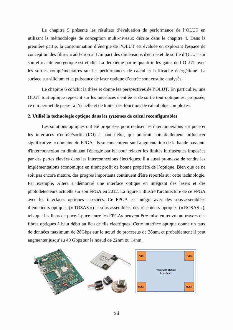
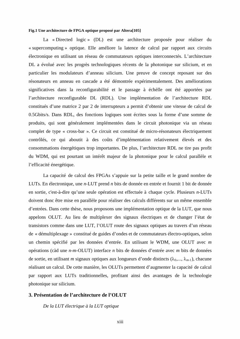
Par exemple, Altera a démontré une interface optique en intégrant des lasers et des
photodétecteurs actuelle sur son FPGA en 2012. La figure 1 illustre l'architecture de ce FPGA
avec les interfaces optiques associées. Ce FPGA est intégré avec des sous-assemblées
d’émetteurs optiques (« TOSAS ») et sous-assemblées des récepteurs optiques (« ROSAS »),
tels que les liens de puce-à-puce entre les FPGAs peuvent être mise en œuvre au travers des
fibres optiques à haut débit au lieu de fils électriques. Cette interface optique donne un taux
de données maximum de 28Gbps sur le nœud de processus de 28nm, et probablement il peut
augmenter jusqu’au 40 Gbps sur le noeud de 22nm ou 14nm.
xiii
Fig.1 Une architecture de FPGA optique proposé par Altera[105]
La « Directed logic » (DL) est une architecture proposée pour réaliser du
« supercomputing » optique. Elle améliore la latence de calcul par rapport aux circuits
électronique en utilisant un réseau de commutateurs optiques interconnectés. L’architecture
DL a évolué avec les progrès technologiques récents de la photonique sur silicium, et en
particulier les modulateurs d’anneau silicium. Une preuve de concept reposant sur des
résonateurs en anneau en cascade a été démontrée expérimentalement. Des améliorations
significatives dans la reconfigurabilité et le passage à échèlle ont été apportées par
l’architecture reconfigurable DL (RDL). Une implémentation de l’architecture RDL
constitués d’une matrice 2 par 2 de interrupteurs a permit d’obtenir une vitesse de calcul de
0.5Gbits/s. Dans RDL, des fonctions logiques sont écrites sous la forme d’une somme de
produits, qui sont généralement implémentées dans le circuit photonique via un réseau
complet de type « cross-bar ». Ce circuit est constitué de micro-résonateurs électriquement
contrôlés, ce qui aboutit à des coûts d’implémentation relativement élevés et des
consommations énergétiques trop importantes. De plus, l’architecture RDL ne tire pas profit
du WDM, qui est pourtant un intérêt majeur de la photonique pour le calcul parallèle et
l’efficacité énergétique.
La capacité de calcul des FPGAs s’appuie sur la petite taille et le grand nombre de
LUTs. En électronique, une n-LUT prend n bits de donnée en entrée et fournit 1 bit de donnée
en sortie, c'est-à-dire qu’une seule opération est effectuée à chaque cycle. Plusieurs n-LUTs
doivent donc être mise en parallèle pour réaliser des calculs différents sur un même ensemble
d’entrées. Dans cette thèse, nous proposons une implémentation optique de la LUT, que nous
appelons OLUT. Au lieu de multiplexer des signaux électriques et de changer l’état de
transistors comme dans une LUT, l’OLUT route des signaux optiques au travers d’un réseau
de « démultiplexage » constitué de guides d’ondes et de commutateurs électro-optiques, selon
un chemin spécifié par les données d’entrée. En utilisant le WDM, une OLUT avec m
opérations (càd une n-m-OLUT) interface n bits de données d’entrée avec m bits de données
de sortie, en utilisant m signaux optiques aux longueurs d’onde distincts (λ0,..., λm-1), chacune
réalisant un calcul. De cette manière, les OLUTs permettent d’augmenter la capacité de calcul
par rapport aux LUTs traditionnelles, profitant ainsi des avantages de la technologie
photonique sur silicium.
3. Présentation de l’architecture de l’OLUT
De la LUT électrique à la LUT optique
xiv
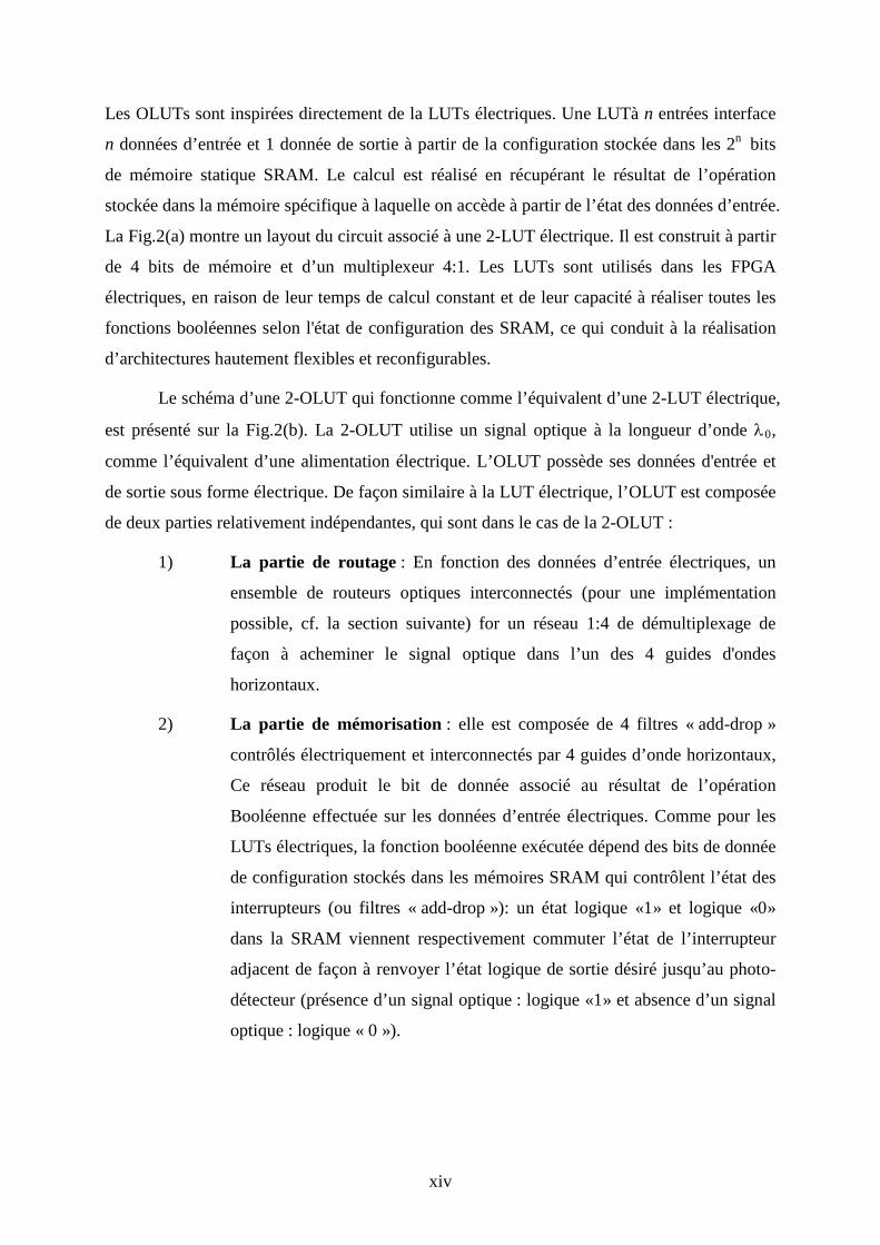
Les OLUTs sont inspirées directement de la LUTs électriques. Une LUTà n entrées interface
n données d’entrée et 1 donnée de sortie à partir de la configuration stockée dans les 2n bits
de mémoire statique SRAM. Le calcul est réalisé en récupérant le résultat de l’opération
stockée dans la mémoire spécifique à laquelle on accède à partir de l’état des données d’entrée.
La Fig.2(a) montre un layout du circuit associé à une 2-LUT électrique. Il est construit à partir
de 4 bits de mémoire et d’un multiplexeur 4:1. Les LUTs sont utilisés dans les FPGA
électriques, en raison de leur temps de calcul constant et de leur capacité à réaliser toutes les
fonctions booléennes selon l'état de configuration des SRAM, ce qui conduit à la réalisation
d’architectures hautement flexibles et reconfigurables.
Le schéma d’une 2-OLUT qui fonctionne comme l’équivalent d’une 2-LUT électrique,
est présenté sur la Fig.2(b). La 2-OLUT utilise un signal optique à la longueur d’onde λ0,
comme l’équivalent d’une alimentation électrique. L’OLUT possède ses données d'entrée et
de sortie sous forme électrique. De façon similaire à la LUT électrique, l’OLUT est composée
de deux parties relativement indépendantes, qui sont dans le cas de la 2-OLUT :
1) La partie de routage : En fonction des données d’entrée électriques, un
ensemble de routeurs optiques interconnectés (pour une implémentation
possible, cf. la section suivante) for un réseau 1:4 de démultiplexage de
façon à acheminer le signal optique dans l’un des 4 guides d'ondes
horizontaux.
2) La partie de mémorisation : elle est composée de 4 filtres « add-drop »
contrôlés électriquement et interconnectés par 4 guides d’onde horizontaux,
Ce réseau produit le bit de donnée associé au résultat de l’opération
Booléenne effectuée sur les données d’entrée électriques. Comme pour les
LUTs électriques, la fonction booléenne exécutée dépend des bits de donnée
de configuration stockés dans les mémoires SRAM qui contrôlent l’état des
interrupteurs (ou filtres « add-drop »): un état logique «1» et logique «0»
dans la SRAM viennent respectivement commuter l’état de l’interrupteur
adjacent de façon à renvoyer l’état logique de sortie désiré jusqu’au photo-
détecteur (présence d’un signal optique : logique «1» et absence d’un signal
optique : logique « 0 »).

xv
0/1
y z0
λ0
λ0
λ0
λ0
D
SRAM Multiplexer
λ00/1
xy
Z0
xInput Data Input Data Output Data
Output Data
(b) Optical 2-LUT
SRAM
(a) Electrical 2-LUT
λ0 stage
0/1
0/1
0/1
Routing Memorization
λ00/1
λ00/1
λ00/1
0/10/1
y z0
λ0
λ0
λ0
λ0
D
SRAM Multiplexer
λ00/1 λ00/1
xy
Z0
xInput Data Input Data Output Data
Output Data
(b) Optical 2-LUT
SRAM
(a) Electrical 2-LUT
λ0 stage
0/10/1
0/10/1
0/10/1
Routing Memorization
λ00/1 λ00/1
λ00/1 λ00/1
λ00/1 λ00/1
Fig.2 Representation schematique d’une (a) 2-LUT electrique et (b) de l’OLUT équivalente.
Principe de base et l’opération du switch
Le composant clé de l’OLUT est le commutateur (ou filtre add-drop). Ces composants
permettent de sélectionner et de rediriger un signal optique en fonction de sa longueur d'onde.
Par souci de clarté, dans la figure 2, on utilise des symboles différents pour représenter les
routeurs optiques et les commutateurs optiques dans la partie de routage et de mémorisation,
respectivement, même si ces fonctions peuvent être physiquement implémentés par le même
composant optique, par exemple un filtre « add-drop » exploitant un micro-résonateur en
anneau (comme expliqué dans la section suivante). La pertinence de cette distinction
deviendra plus explicite lors de l'introduction de l'utilisation du WDM dans les architectures
OLUTs pour paralléliser les calculs.
Pour une géométrie et des paramètres matériaux donnés, le spectre de transmission
d’un filtre add-drop à micro-anneau est typiquement un peigne de raies qui peut être modifié
par un signal de contrôle, conduisant à la définition d’un état « Through » et d’un état
« Drop » :
« Etat Through»: la résonance du filtre add-drop (i.e. associé à un pic de transmission)
est désalignée spectralement avec la longueur d’onde du signal d’entrée, de sorte que le signal
optique continue sur le même guide d’onde, sans être perturbé par le filtre add-drop qu’il
croise.
«Etat Drop» : la résonance du filtre add-drop est alignée avec la longueur d’onde du
signal d’entrée, de sorte que ce dernier est redirigé du guide d’onde d’entrée vers le second
guide (dans l’exemple de la Fig.2, le guide orthogonal).
Le commutateur ainsi implémenté peut être considéré comme un routeur optique
spatial 1x2 contrôlé dynamiquement (i.e. le bloc de base dans la partie routage) ou bien
xvi
comme un interrupteur optique contrôlé statiquement qui peut changer la direction du signal
optique d’entrée en fonction de l’état de donnée stockée dans la mémoire adjacent (i.e. la
brique de base pour implémenter la partie de mémorisation). Noter que les cahiers des charges
pour ces deux fonctions sont cependant assez différents: le commutateur de la partie routage
doit pouvoir fonctionner en régime de modulation dynamique très rapide, pour être
compatible avec un débit de données (signale de contrôle) élevé, tandis que le commutateur
de la partie mémorisation n’impose aucune exigence sur la vitesse de modulation puisqu’il
fonctionne à l'état statique et n’est modifié que de manière ponctuelle si l’OLUT est
reconfigurée. Pour le reste du résumé, nous utilisons de manière équivalente le terme de filtre
«add-drop » pour désigner ces deux composants. Enfin, bien que le symbole choisi pour
représenter le commutateur optique ressemble à un micro-anneau, nous soulignons que cela
ne représente qu’un choix d’implémentation possible (probablement la plus mature
actuellement) pour construire les commutateurs composant l’architecture de l’OLUT.
1
0
0
0
0 1
0
AND
1
0
0
0
1 1
1
AND
D
1
λ0
λ0
λ0 0
0
0
λ0
1 1 1AND D
1
λ0
λ0
λ0 0
0
0
λ0
1 0 0AND
1
0
0
0
0 0
0
AND
D
1
λ0
λ0
λ0 0
0
0
λ0
0 0 0AND
1
0
0
0
1 0
0
AND
Electrical 2-LUT
2-1x2-OLUT
a) b) c) d)
e) f) g) h)D
1
λ0
λ0
λ0 0
0
0
λ0
0 1 0AND
1
0
0
0
0 1
0
AND
1
0
0
0
0 1
0
AND
1
0
0
0
1 1
1
AND
1
0
0
0
1 1
1
AND
D
11
λ0
λ0
λ0 00
00
0
λ0λ0λ0
1 1 1AND D
1
λ0
λ0
λ0 00
00
0
λ0
1 0 0AND
1
0
0
0
0 0
0
AND
1
0
0
0
0 0
0
AND
D
11
λ0
λ0
λ0 0
0
0
λ0
0 0 0AND
1
0
0
0
1 0
0
AND
1
0
0
0
1 0
0
AND
Electrical 2-LUT
2-1x2-OLUT
a) b) c) d)
e) f) g) h)D
11
λ0
λ0
λ0 0
0
0
λ0
0 1 0AND
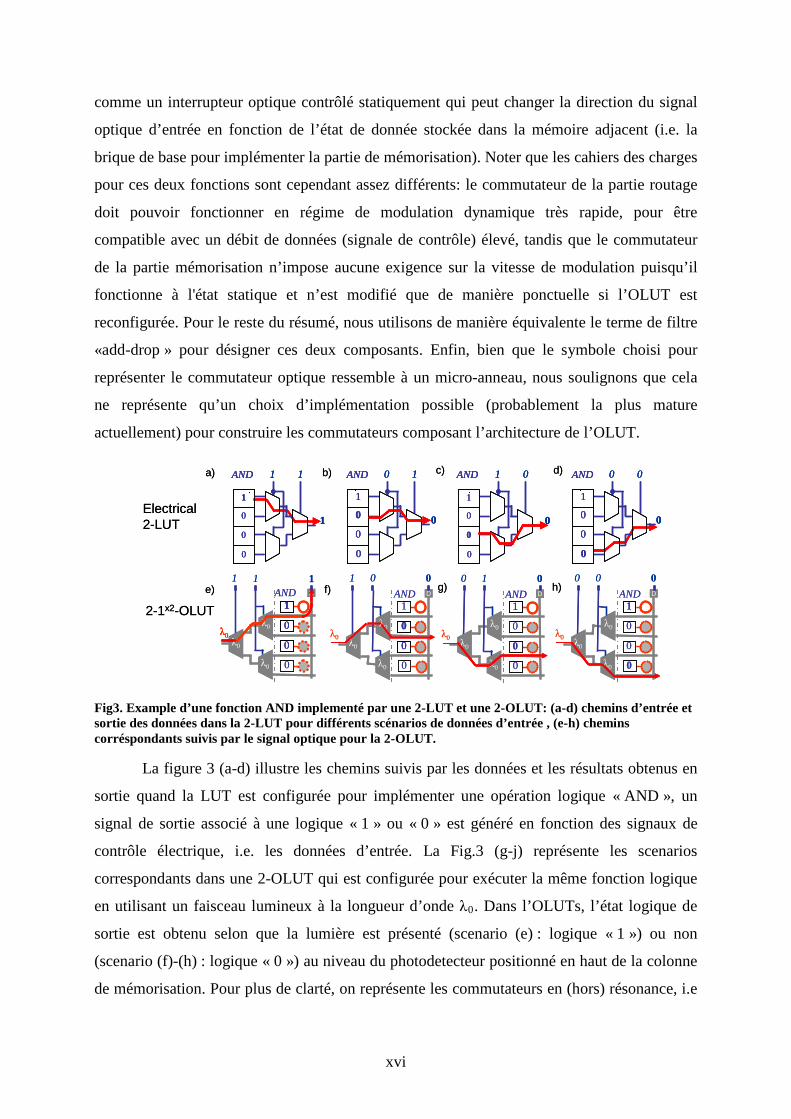
Fig3. Example d’une fonction AND implementé par une 2-LUT et une 2-OLUT: (a-d) chemins d’entrée et sortie des données dans la 2-LUT pour différents scénarios de données d’entrée , (e-h) chemins corréspondants suivis par le signal optique pour la 2-OLUT.
La figure 3 (a-d) illustre les chemins suivis par les données et les résultats obtenus en
sortie quand la LUT est configurée pour implémenter une opération logique « AND », un
signal de sortie associé à une logique « 1 » ou « 0 » est généré en fonction des signaux de
contrôle électrique, i.e. les données d’entrée. La Fig.3 (g-j) représente les scenarios
correspondants dans une 2-OLUT qui est configurée pour exécuter la même fonction logique
en utilisant un faisceau lumineux à la longueur d’onde λ0. Dans l’OLUTs, l’état logique de
sortie est obtenu selon que la lumière est présenté (scenario (e) : logique « 1 ») ou non
(scenario (f)-(h) : logique « 0 ») au niveau du photodetecteur positionné en haut de la colonne
de mémorisation. Pour plus de clarté, on représente les commutateurs en (hors) résonance, i.e
xvii
qui sont spectralement (des)alignés avec le signal optique incident par les contours des rings
en trait plain (pointillé).
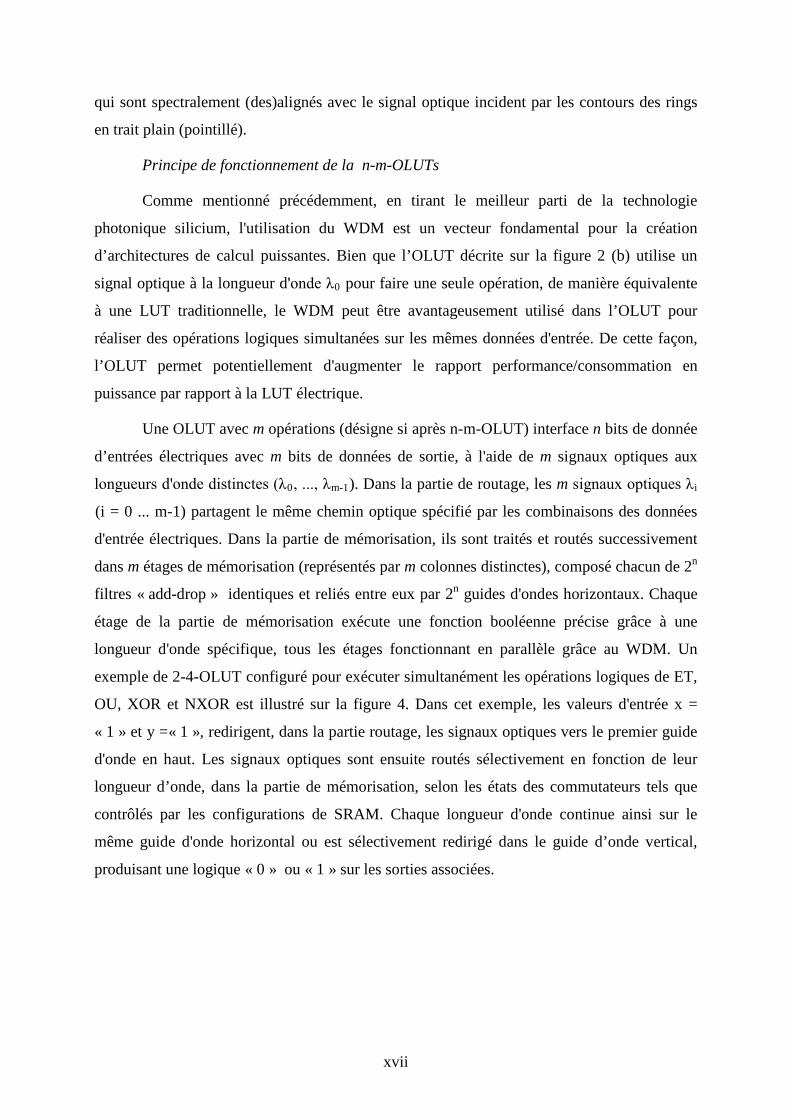
Principe de fonctionnement de la n-m-OLUTs
Comme mentionné précédemment, en tirant le meilleur parti de la technologie
photonique silicium, l'utilisation du WDM est un vecteur fondamental pour la création
d’architectures de calcul puissantes. Bien que l’OLUT décrite sur la figure 2 (b) utilise un
signal optique à la longueur d'onde λ0 pour faire une seule opération, de manière équivalente
à une LUT traditionnelle, le WDM peut être avantageusement utilisé dans l’OLUT pour
réaliser des opérations logiques simultanées sur les mêmes données d'entrée. De cette façon,
l’OLUT permet potentiellement d'augmenter le rapport performance/consommation en
puissance par rapport à la LUT électrique.
Une OLUT avec m opérations (désigne si après n-m-OLUT) interface n bits de donnée
d’entrées électriques avec m bits de données de sortie, à l'aide de m signaux optiques aux
longueurs d'onde distinctes (λ0, ..., λm-1). Dans la partie de routage, les m signaux optiques λi
(i = 0 ... m-1) partagent le même chemin optique spécifié par les combinaisons des données
d'entrée électriques. Dans la partie de mémorisation, ils sont traités et routés successivement
dans m étages de mémorisation (représentés par m colonnes distinctes), composé chacun de 2n
filtres « add-drop » identiques et reliés entre eux par 2n guides d'ondes horizontaux. Chaque
étage de la partie de mémorisation exécute une fonction booléenne précise grâce à une
longueur d'onde spécifique, tous les étages fonctionnant en parallèle grâce au WDM. Un
exemple de 2-4-OLUT configuré pour exécuter simultanément les opérations logiques de ET,
OU, XOR et NXOR est illustré sur la figure 4. Dans cet exemple, les valeurs d'entrée x =
« 1 » et y =« 1 », redirigent, dans la partie routage, les signaux optiques vers le premier guide
d'onde en haut. Les signaux optiques sont ensuite routés sélectivement en fonction de leur
longueur d’onde, dans la partie de mémorisation, selon les états des commutateurs tels que
contrôlés par les configurations de SRAM. Chaque longueur d'onde continue ainsi sur le
même guide d'onde horizontal ou est sélectivement redirigé dans le guide d’onde vertical,
produisant une logique « 0 » ou « 1 » sur les sorties associées.

xviii
YX
1
Routing part Memorization part
1
1 1
1
1
0
0 1
0
0
0
1
0
λx
λx
D D D D
λ0
λ0
λ0
λ0
λ1
λ1
λ1
λ1 λ2
λ2
λ2
λ2
λ3
0 λ3
λ3
0 λ3
AND OR XOR Buffer
λ0λ1λ2λ3
Z0 Z1 Z2 Z3‘1’ ‘1’ ‘1’ ‘1’ ‘1’‘0’
λx
YX
1
Routing part Memorization part
1
1 1
1
1
0
0 1
0
0
0
1
0
λx
λx
D D D D
λ0
λ0
λ0
λ0
λ1
λ1
λ1
λ1 λ2
λ2
λ2
λ2
λ3
0 λ30 λ3
λ3
0 λ30 λ3
AND OR XOR Buffer
λ0λ1λ2λ3
Z0 Z1 Z2 Z3‘1’ ‘1’ ‘1’ ‘1’ ‘1’‘0’
λx
Fig.4 Représentation fonctionnelle d'une 2-4-OLUT configurée pour réaliser en parallèle 4 opérations logiques sur 4 longueurs d'onde distinctes.
Dans l'architecture de l’OLUT, le WDM est mis en œuvre à l'aide de deux schémas
distincts de filtrage en longueur d'onde (i) dans la partie de routage, où tous les signaux
optiques, indépendamment de leur longueur d'onde, se propagent le long du même chemin, et
(ii) dans la partie de mémorisation, où chaque signal optique (qui est spectralement distincte
des autres) est acheminé individuellement en fonction de la donnée de configuration. Pour
l'exemple de la 2-4-OLUT (Fig.4):
La partie de routage: Le comportement du commutateur dans la partie de routage est
illustré sur la Fig.5 (a) selon qu’il est dans l’état Drop (trait plein) ou dans l’état Through
(ligne pointillée). Les flèches représentent les quatre signaux optiques incidents pour lesquels
les longueurs d'onde λ0, λ1, λ2 et λ3 sont soit idéalement alignées avec les longueurs d'onde
de résonance du filtre add-drop (représentés par des pics dans le spectre de transmission) dans
l'état Drop, soit désaccordées avec un certain écart en longueur d'onde ∆λ dans l'état Through.
Les longueurs d'onde des signaux optiques injectés sont régulièrement espacées d’un écart
spectral correspondant au FSRx (« free spectral range ») du filtre add-drop. Ainsi, dans le cas
où le filtre « add-drop » est dans l'état DROP, tous les signaux sont redirigés vers un guide
d'onde donné, alors que dans l'état Through, tous les signaux se propagent le long de l'autre
guide d'onde.
La partie de mémorisation: Les Fig.5 (b) et (c) illustrent le fonctionnement des
filtres « add-drop » dans la partie de mémorisation ainsi que leur spectre de transmission. Par
rapport à ceux de la partie de routage, leur FSR est légèrement plus large (notés FSRm0 et
dans FSRm1 sur les Fig.5 (b) et (c)) de sorte qu’une seule longueur d'onde de résonance se
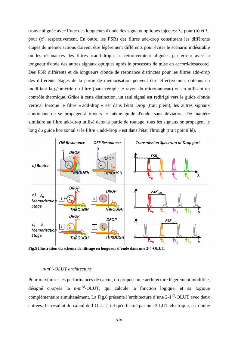
xix
trouve alignée avec l’une des longueurs d'onde des signaux optiques injectés: λ0 pour (b) et λ1
pour (c), respectivement. En outre, les FSRs des filtres add-drop constituant les différents
étages de mémorisations doivent être légèrement différents pour éviter le scénario indésirable
où les résonances des filtres « add-drop » se retrouveraient alignées par erreur avec la
longueur d'onde des autres signaux optiques après le processus de mise en accord/désaccord.
Des FSR différents et de longueurs d'onde de résonance distinctes pour les filtres add-drop
des différents étages de la partie de mémorisation peuvent être effectivement obtenus en
modifiant la géométrie du filtre (par exemple le rayon du micro-anneau) ou en utilisant un
contrôle thermique. Grâce à cette distinction, un seul signal est redirigé vers le guide d'onde
vertical lorsque le filtre « add-drop » est dans l'état Drop (trait plein), les autres signaux
continuant de se propager à travers le même guide d'onde, sans déviation. De manière
similaire au filtre add-drop utilisé dans la partie de routage, tous les signaux se propagent le
long du guide horizontal si le filtre « add-drop » est dans l'état Through (trait pointillé).
1λ0λ1λ2λ3λx
0
λx λ0λ2λ3
λ1
FSRx
λλ0 λ1 λ2 λ3
ON Resonance OFF Resonance
1
0
λ0
λ1λ2λ3
λ01
λ0λ1λ2λ3
λ00
FSRm0
λλ0 λ1 λ2 λ3
1
0
λ1
λ0λ2λ3
λ11
λ0λ1λ2λ3
λ10
FSRm1
λλ0 λ1 λ2 λ3
1
0
THROUGH
a) Router
b) λ0
λ1
Transmission Spectrum at Drop port
DROP
DROP
DROP
THROUGH
DROP
THROUGH
DROP
THROUGH
DROP
THROUGH
THROUGH
Memorization Stage
c)Memorization Stage
1λ0λ1λ2λ3
λ0λ1λ2λ3λx
0
λx λ0λ2λ3
λ1
FSRx
λλ0 λ1 λ2 λ3
ON Resonance OFF Resonance
1
0
λ0
λ1λ2λ3
λ01
λ0λ1λ2λ3
λ00
FSRm0
λλ0 λ1 λ2 λ3
1
0
λ1
λ0λ2λ3
λ11
λ0λ1λ2λ3
λ10
FSRm1
λλ0 λ1 λ2 λ3
1
0
THROUGH
a) Router
b) λ0
λ1
Transmission Spectrum at Drop port
DROP
DROP
DROP
THROUGH
DROP
THROUGH
DROP
THROUGH
DROP
THROUGH
THROUGH
Memorization Stage
c)Memorization Stage
Fig.5 Illustration du schéma de filtrage en longueur d’onde dans une 2-4-OLUT.
n-mx2-OLUT architecture
Pour maximiser les performances de calcul, on propose une architecture légèrement modifiée,
désigné ci-après la n-m×2-OLUT, qui calcule la fonction logique, et sa logique
complémentaire simultanément. La Fig.6 présente l’architecture d’une 2-1×2-OLUT avec deux
entrées. Le résultat du calcul de l’OLUT, tel qu'effectué par une 2-LUT électrique, est donné
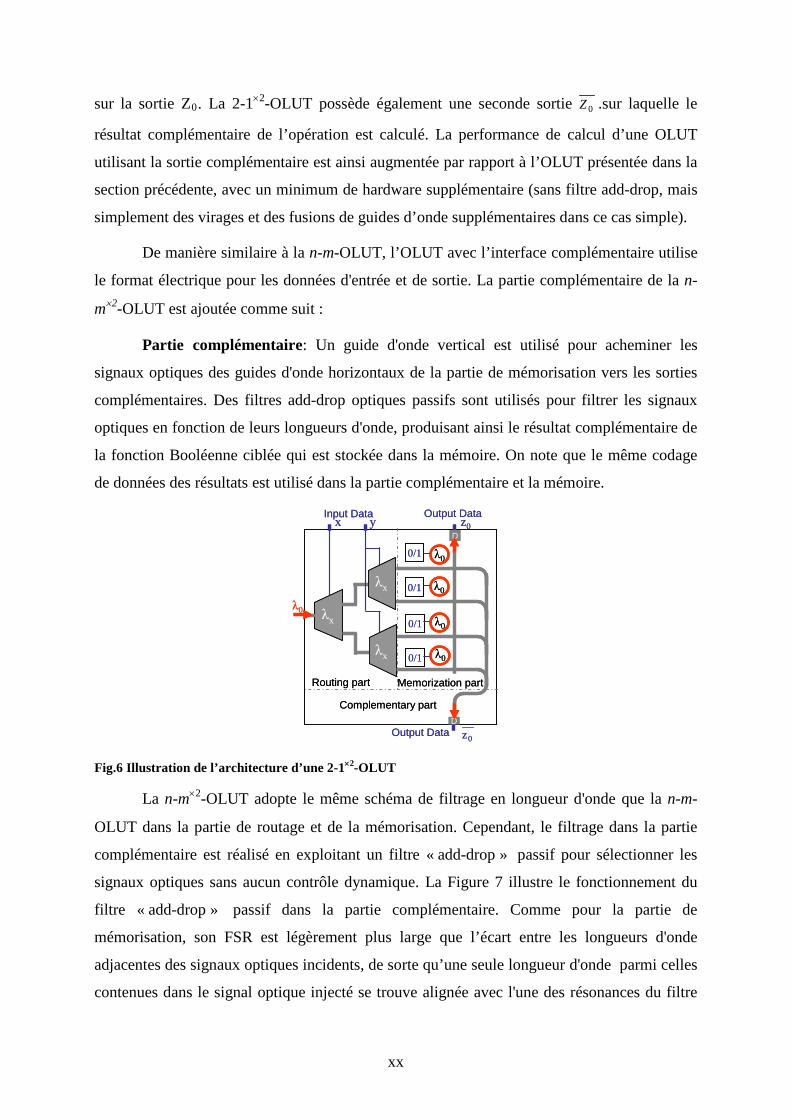
xx
sur la sortie Z0. La 2-1×2-OLUT possède également une seconde sortie 0Z .sur laquelle le
résultat complémentaire de l’opération est calculé. La performance de calcul d’une OLUT
utilisant la sortie complémentaire est ainsi augmentée par rapport à l’OLUT présentée dans la
section précédente, avec un minimum de hardware supplémentaire (sans filtre add-drop, mais
simplement des virages et des fusions de guides d’onde supplémentaires dans ce cas simple).
De manière similaire à la n-m-OLUT, l’OLUT avec l’interface complémentaire utilise
le format électrique pour les données d'entrée et de sortie. La partie complémentaire de la n-
m×2-OLUT est ajoutée comme suit :
Partie complémentaire: Un guide d'onde vertical est utilisé pour acheminer les
signaux optiques des guides d'onde horizontaux de la partie de mémorisation vers les sorties
complémentaires. Des filtres add-drop optiques passifs sont utilisés pour filtrer les signaux
optiques en fonction de leurs longueurs d'onde, produisant ainsi le résultat complémentaire de
la fonction Booléenne ciblée qui est stockée dans la mémoire. On note que le même codage
de données des résultats est utilisé dans la partie complémentaire et la mémoire.
yx
0/1
Routing part Memorization part
0/1
0/1
0/1
λx
λx
λx
λ0
0z
z0D
λ0
λ0
λ0
λ0
Complementary part
Input Data Output Data
Output Data D
yx
0/1
Routing part Memorization part
0/1
0/1
0/1
λx
λx
λx
λ0
0z
z0D
λ0
λ0
λ0
λ0
Complementary part
Input Data Output Data
Output Data D
Fig.6 Illustration de l’architecture d’une 2-1×2-OLUT
La n-m×2-OLUT adopte le même schéma de filtrage en longueur d'onde que la n-m-
OLUT dans la partie de routage et de la mémorisation. Cependant, le filtrage dans la partie
complémentaire est réalisé en exploitant un filtre « add-drop » passif pour sélectionner les
signaux optiques sans aucun contrôle dynamique. La Figure 7 illustre le fonctionnement du
filtre « add-drop » passif dans la partie complémentaire. Comme pour la partie de
mémorisation, son FSR est légèrement plus large que l’écart entre les longueurs d'onde
adjacentes des signaux optiques incidents, de sorte qu’une seule longueur d'onde parmi celles
contenues dans le signal optique injecté se trouve alignée avec l'une des résonances du filtre
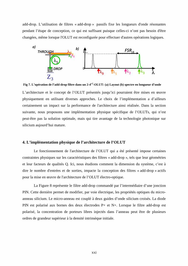
xxi
add-drop. L’utilisation de filtres « add-drop » passifs fixe les longueurs d'onde résonantes
pendant l’étape de conception, ce qui est suffisant puisque celles-ci n’ont pas besoin d'être
changées, même lorsque l'OLUT est reconfigurée pour effectuer d'autres opérations logiques.
λ2
λ0λ1
λλ0 λ1 λ2 λ3
1
0D
λ3
λ3
FSRi3
3ZDROP
THROUGHa) b)
λ2
λ0λ1
λλ0 λ1 λ2 λ3
1
0D
λ3
λ3
FSRi3
3ZDROP
THROUGHa) b)
Fig 7. L’opération de l’add-drop filtre dans un 2-4×2-OLUT: (a) Layout (b) spectre en longueur d’onde
L’architecture et le concept de l’OLUT présentés jusqu’ici pourraient être mises en œuvre
physiquement en utilisant diverses approches. Le choix de l’implémentation a d’ailleurs
certainement un impact sur la performance de l'architecture ainsi réalisée. Dans la section
suivante, nous proposons une implémentation physique spécifique de l’OLUTs, qui n’est
peut-être pas la solution optimale, mais qui tire avantage de la technologie photonique sur
silicium aujourd’hui mature.
4. L’implémentation physique de l’architecture de l’OLUT
Le fonctionnement de l'architecture de l’OLUT qui a été présenté impose certaines
contraintes physiques sur les caractéristiques des filtres « add-drop », tels que leur géométries
et leur facteurs de qualités Q. Ici, nous étudions comment la dimension du système, c’est à
dire le nombre d'entrées et de sorties, impacte la conception des filtres « add-drop » actifs
pour la mise en œuvre de l'architecture de l’OLUT électro-optique.
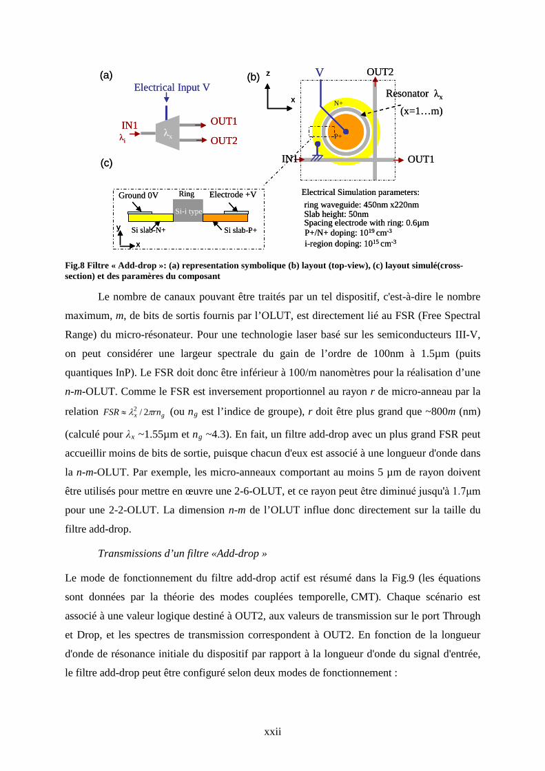
La Figure 8 représente le filtre add-drop commandé par l’intermédiaire d’une jonction
PIN. Cette dernière permet de modifier, par voie électrique, les propriétés optiques du micro-
anneau silicium. Le micro-anneau est couplé à deux guides d’onde silicium croisés. La diode
PIN est polarisé aux bornes des deux électrodes P+ et N+. Lorsque le filtre add-drop est
polarisé, la concentration de porteurs libres injectés dans l’anneau peut être de plusieurs
ordres de grandeur supérieur à la densité intrinsèque initiale.
xxii
Electrical Input V
OUT2
OUT1IN1λi
λx P+
V
N+
IN1 OUT1
OUT2
Resonator λx
(x=1…m)
(a) (b)
y
x
z
x
(c)
ring waveguide: 450nm x220nmSlab height: 50nmSpacing electrode with ring: 0.6µmP+/N+ doping: 1019 cm-3
i-region doping: 1015 cm-3
Electrical Simulation parameters:
Si slab-P+
Ring Electrode +V
Si slab-N+
Ground 0V
Si-i type
Electrical Input V
OUT2
OUT1IN1λi
λx P+
V
N+
IN1 OUT1
OUT2
Resonator λx
(x=1…m)
(a) (b)
y
x
y
x
z
x
z
x
(c)
ring waveguide: 450nm x220nmSlab height: 50nmSpacing electrode with ring: 0.6µmP+/N+ doping: 1019 cm-3
i-region doping: 1015 cm-3
Electrical Simulation parameters:
Si slab-P+
Ring Electrode +V
Si slab-N+
Ground 0V
Si-i type
Fig.8 Filtre « Add-drop »: (a) representation symbolique (b) layout (top-view), (c) layout simulé(cross-section) et des paramères du composant
Le nombre de canaux pouvant être traités par un tel dispositif, c'est-à-dire le nombre
maximum, m, de bits de sortis fournis par l’OLUT, est directement lié au FSR (Free Spectral
Range) du micro-résonateur. Pour une technologie laser basé sur les semiconducteurs III-V,
on peut considérer une largeur spectrale du gain de l’ordre de 100nm à 1.5µm (puits
quantiques InP). Le FSR doit donc être inférieur à 100/m nanomètres pour la réalisation d’une
n-m-OLUT. Comme le FSR est inversement proportionnel au rayon r de micro-anneau par la
relation gx rnFSR πλ 2/2≈ (ou ng est l’indice de groupe), r doit être plus grand que ~800m (nm)
(calculé pour λx ~1.55µm et ng ~4.3). En fait, un filtre add-drop avec un plus grand FSR peut
accueillir moins de bits de sortie, puisque chacun d'eux est associé à une longueur d'onde dans
la n-m-OLUT. Par exemple, les micro-anneaux comportant au moins 5 µm de rayon doivent
être utilisés pour mettre en œuvre une 2-6-OLUT, et ce rayon peut être diminué jusqu'à 1.7μm
pour une 2-2-OLUT. La dimension n-m de l’OLUT influe donc directement sur la taille du
filtre add-drop.
Transmissions d’un filtre «Add-drop »
Le mode de fonctionnement du filtre add-drop actif est résumé dans la Fig.9 (les équations
sont données par la théorie des modes couplées temporelle, CMT). Chaque scénario est
associé à une valeur logique destiné à OUT2, aux valeurs de transmission sur le port Through
et Drop, et les spectres de transmission correspondent à OUT2. En fonction de la longueur
d'onde de résonance initiale du dispositif par rapport à la longueur d'onde du signal d'entrée,
le filtre add-drop peut être configuré selon deux modes de fonctionnement :
xxiii
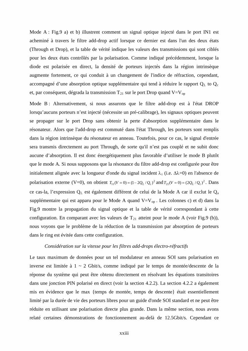
Mode A : Fig.9 a) et b) illustrent comment un signal optique injecté dans le port IN1 est
acheminé à travers le filtre add-drop actif lorsque ce dernier est dans l'un des deux états
(Through et Drop), et la table de vérité indique les valeurs des transmissions qui sont ciblés
pour les deux états contrôlés par la polarisation. Comme indiqué précédemment, lorsque la
diode est polarisée en direct, la densité de porteurs injectés dans la région intrinsèque
augmente fortement, ce qui conduit à un changement de l'indice de réfraction, cependant,
accompagné d’une absorption optique supplémentaire qui tend à réduire le rapport QL to Qc
et, par conséquent, dégrada la transmission T21 sur le port Drop quand V=Vop
Mode B : Alternativement, si nous assurons que le filtre add-drop est à l'état DROP
lorsqu’aucuns porteurs n’est injecté (nécessite un pré-calibrage), les signaux optiques peuvent
se propager sur le port Drop sans obtenir la perte d'absorption supplémentaire dans le
résonateur. Alors que l'add-drop est commuté dans l'état Through, les porteurs sont remplis
dans la région intrinsèque du résonateur en anneau. Toutefois, pour ce cas, le signal d'entrée
sera transmis directement au port Through, de sorte qu'il n’est pas couplé et ne subit donc
aucune d’absorption. Il est donc énergétiquement plus favorable d’utiliser le mode B plutôt
que le mode A. Si nous supposons que la résonance du filtre add-drop est configurée pour être
initialement alignée avec la longueur d'onde du signal incident λ i (i.e. ∆λ=0) en l'absence de
polarisation externe (V=0), on obtient 211 )/21()0( cL QQVT −== and 2
21 )/2()0( cL QQVT == . Dans
ce cas-la, l’expression QL est également différent de celui de la Mode A car il exclut le Qa
supplémentaire qui est apparu pour le Mode A quand V=Vop . Les colonnes c) et d) dans la
Fig.9 montre la propagation du signal optique et la table de vérité correspondant à cette
configuration. En comparant avec les valeurs de T21 atteint pour le mode A (voir Fig.9 (b)),
nous voyons que le problème de la réduction de la transmission par absorption de porteurs
dans le ring est évitée dans cette configuration.
Considération sur la vitesse pour les filtres add-drops électro-réfractifs
Le taux maximum de données pour un tel modulateur en anneau SOI sans polarisation en
inverse est limitée à 1 ~ 2 Gbit/s, comme indiqué par le temps de montée/descente de la
réponse du système qui peut être obtenu directement en résolvant les équations transitoires
dans une jonction PIN polarisé en direct (voir la section 4.2.2). La section 4.2.2 a également
mis en évidence que le max {temps de montée, temps de descente} était essentiellement
limité par la durée de vie des porteurs libres pour un guide d'onde SOI standard et ne peut être
réduite en utilisant une polarisation directe plus grande. Dans la même section, nous avons
relaté certaines démonstrations de fonctionnement au-delà de 12.5Gbit/s. Cependant ce

xxiv
régime nécessite l’implémentation de signaux électriques complexes et de tensions élevées,
peu compatible avec un circuit de contrôle CMOS de faible consommation.
a) Mode A (V=0) b) Mode A (V=Vop) c) Mode B (V=0) d) Mode B (V=Vop)
Signal propagati
on scenario
THROUGH
IN
V=0
OUT2
OUT1
IN2
THROUGH
IN
V=0
OUT2
OUT1
IN2
DROP
IN
V≠0OUT2
OUT1
IN2
DROP
IN
V≠0OUT2
OUT1
IN2
DROP
IN
V=0OUT2
OUT1
IN2
DROP
IN
V=0OUT2
OUT1
IN2
THROUGH
IN1
V≠0
OUT2
OUT1
IN2
THROUGH
IN1
V≠0
OUT2
OUT1
IN2 Targeted
Signal logic at OUT2
‘0’ ‘1’ ‘1’ ‘0’
T11 [ ] 1/2)/21(1
1 2
2
+∆
−−−
λλL
cL
QQQ 2)
//2//
(acic
acic
QQQQQQQQ
+++ 2)
/2/(
ic
ic
QQQQ
+
[ ] 1/2)/21(1
1 2
2
+∆
−−−
λλL
cL
QQQ
T21 [ ] 1/2
)/2(2
2
+∆ λλL
cL
QQQ
2)
//22(
acic QQQQ ++
2)/2
2(ic QQ+
[ ] 1/2
)/2(2
2
+∆ λλL
cL
QQQ
Spectrum
λ
λi
T21
λres λ
λi
T21
λres λ
T21
λres
λi
λ
T21
λres
λi
λ
λiT21
λres λ
λiT21
λres λ
λi
T21
λres λ
λi
T21
λres Fig.9 Fonctionnement du filtre add-drop actif selon les 2 modes opératoires A et B.
5. Méthodologie pour l’évaluation de la performance
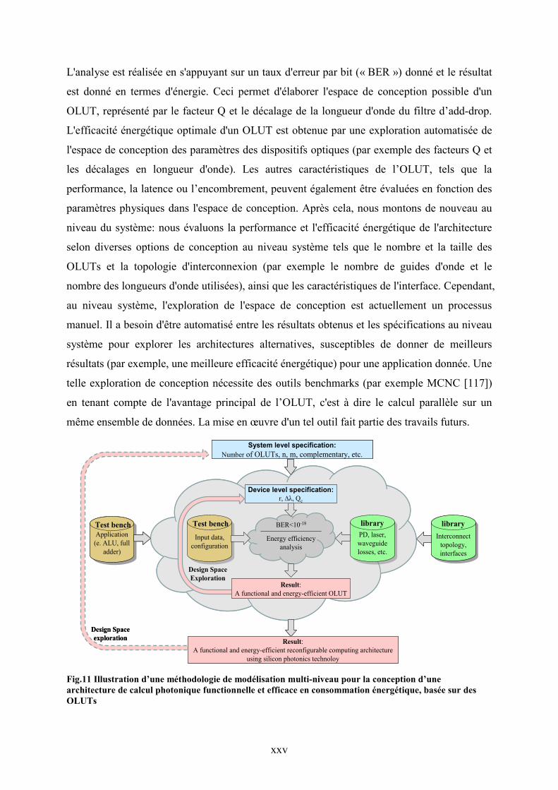
Fig.10 illustre la méthodologie de conception. Idéalement, pour une application de calcul
donnée (par exemple un ALU ou un additionneur complet), notre approche commence avec
les spécifications au niveau architectural (notamment en ce qui concerne le nombre de OLUTs,
les dimensions des entrées et des sorties des OLUTs, ainsi que l'option complémentaire) et
passe ensuite progressivement jusqu'au niveau composant afin de concevoir un OLUT
fonctionnel. Les paramètres au niveau du dispositif incluent la taille (rayon de l'anneau), le
facteur de qualité et le décalage de longueur d'onde des filtres add-drop. Ces paramètres
seront utilisés pour évaluer les caractéristiques clés du dispositif optique en effectuant la
simulation physique (par exemple par FDTD), la simulation électrique et la modélisation avec
la théorie des modes couplés (CMT). Les caractéristiques des autres composants (par exemple,
les lasers et les photodétecteurs, ainsi que les guides d'onde) dans la boîte à outils
fonctionnelle utilisant la technologie photonique sur silicium sont extraits de la bibliothèque.
La configuration des données d'entrée et des mémoires différentes (indiquées par l'application
cible) sont considérés pour calculer la consommation d'énergie d'un seul bloc de OLUT.

xxv
L'analyse est réalisée en s'appuyant sur un taux d'erreur par bit (« BER ») donné et le résultat
est donné en termes d'énergie. Ceci permet d'élaborer l'espace de conception possible d'un
OLUT, représenté par le facteur Q et le décalage de la longueur d'onde du filtre d’add-drop.
L'efficacité énergétique optimale d'un OLUT est obtenue par une exploration automatisée de
l'espace de conception des paramètres des dispositifs optiques (par exemple des facteurs Q et
les décalages en longueur d'onde). Les autres caractéristiques de l’OLUT, tels que la
performance, la latence ou l’encombrement, peuvent également être évaluées en fonction des
paramètres physiques dans l'espace de conception. Après cela, nous montons de nouveau au
niveau du système: nous évaluons la performance et l'efficacité énergétique de l'architecture
selon diverses options de conception au niveau système tels que le nombre et la taille des
OLUTs et la topologie d'interconnexion (par exemple le nombre de guides d'onde et le
nombre des longueurs d'onde utilisées), ainsi que les caractéristiques de l'interface. Cependant,
au niveau système, l'exploration de l'espace de conception est actuellement un processus
manuel. Il a besoin d'être automatisé entre les résultats obtenus et les spécifications au niveau
système pour explorer les architectures alternatives, susceptibles de donner de meilleurs
résultats (par exemple, une meilleure efficacité énergétique) pour une application donnée. Une
telle exploration de conception nécessite des outils benchmarks (par exemple MCNC [117])
en tenant compte de l'avantage principal de l’OLUT, c'est à dire le calcul parallèle sur un
même ensemble de données. La mise en œuvre d'un tel outil fait partie des travails futurs.
Device level specification:r, ∆λ, Qc
System level specification:Number of OLUTs, n, m, complementary, etc.
Input data, configurationInput data,
configurationApplication (e. ALU, full
adder)
Application (e. ALU, full
adder)
PD, laser, waveguide losses, etc.
PD, laser, waveguide losses, etc.
Interconnect topology, interfaces
Interconnect topology, interfaces
Energy efficiency analysis
BER<10-18
Result:A functional and energy-efficient OLUT
Result:A functional and energy-efficient reconfigurable computing architecture
using silicon photonics technoloy
library libraryTest benchTest bench
Design Space Exploration
Design Space exploration
Fig.11 Illustration d’une méthodologie de modélisation multi-niveau pour la conception d’une architecture de calcul photonique functionnelle et efficace en consommation énergétique, basée sur des OLUTs
xxv
L'analyse est réalisée en s'appuyant sur un taux d'erreur par bit (« BER ») donné et le résultat
est donné en termes d'énergie. Ceci permet d'élaborer l'espace de conception possible d'un
OLUT, représenté par le facteur Q et le décalage de la longueur d'onde du filtre d’add-drop.
L'efficacité énergétique optimale d'un OLUT est obtenue par une exploration automatisée de
l'espace de conception des paramètres des dispositifs optiques (par exemple des facteurs Q et
les décalages en longueur d'onde). Les autres caractéristiques de l’OLUT, tels que la
performance, la latence ou l’encombrement, peuvent également être évaluées en fonction des
paramètres physiques dans l'espace de conception. Après cela, nous montons de nouveau au
niveau du système: nous évaluons la performance et l'efficacité énergétique de l'architecture
selon diverses options de conception au niveau système tels que le nombre et la taille des
OLUTs et la topologie d'interconnexion (par exemple le nombre de guides d'onde et le
nombre des longueurs d'onde utilisées), ainsi que les caractéristiques de l'interface. Cependant,
au niveau système, l'exploration de l'espace de conception est actuellement un processus
manuel. Il a besoin d'être automatisé entre les résultats obtenus et les spécifications au niveau
système pour explorer les architectures alternatives, susceptibles de donner de meilleurs
résultats (par exemple, une meilleure efficacité énergétique) pour une application donnée. Une
telle exploration de conception nécessite des outils benchmarks (par exemple MCNC [117])
en tenant compte de l'avantage principal de l’OLUT, c'est à dire le calcul parallèle sur un
même ensemble de données. La mise en œuvre d'un tel outil fait partie des travails futurs.
Device level specification:r, ∆λ, Qc
System level specification:Number of OLUTs, n, m, complementary, etc.
Input data, configurationInput data,
configurationApplication (e. ALU, full
adder)
Application (e. ALU, full
adder)
PD, laser, waveguide losses, etc.
PD, laser, waveguide losses, etc.
Interconnect topology, interfaces
Interconnect topology, interfaces
Energy efficiency analysis
BER<10-18
Result:A functional and energy-efficient OLUT
Result:A functional and energy-efficient reconfigurable computing architecture
using silicon photonics technoloy
library libraryTest benchTest bench
Design Space Exploration
Design Space exploration
Device level specification:r, ∆λ, Qc
System level specification:Number of OLUTs, n, m, complementary, etc.
Input data, configuration
Input data, configurationInput data,
configurationApplication (e. ALU, full
adder)
Application (e. ALU, full
adder)
Test benchTest benchApplication Application Application Application
(e. ALU, full Application
(e. ALU, full (e. ALU, full (e. ALU, full (e. ALU, full (e. ALU, full adder
(e. ALU, full adder)
(e. ALU, full )adderadderadderadder)adder))
Application (e. ALU, full
adder)
PD, laser, waveguide losses, etc.
PD, laser, waveguide waveguide losses, etc.losses, etc.
PD, laser, waveguide losses, etc.
Interconnect topology, interfaces
Interconnect topology, interfaces
library
Interconnect Interconnect Interconnect Interconnect topology, topology, topology, topology,
interfacestopology,
interfacesinterfacesinterfacesinterfacesinterfaces
Interconnect topology, interfaces
Energy efficiency analysis
BER<10-18
Result:A functional and energy-efficient OLUT
Result:A functional and energy-efficient reconfigurable computing architecture
using silicon photonics technoloy
library libraryTest benchTest bench
Design Space Exploration
Design Space exploration
Fig.11 Illustration d’une méthodologie de modélisation multi-niveau pour la conception d’une architecture de calcul photonique functionnelle et efficace en consommation énergétique, basée sur des OLUTs

xxvi
Modèle d’énergie
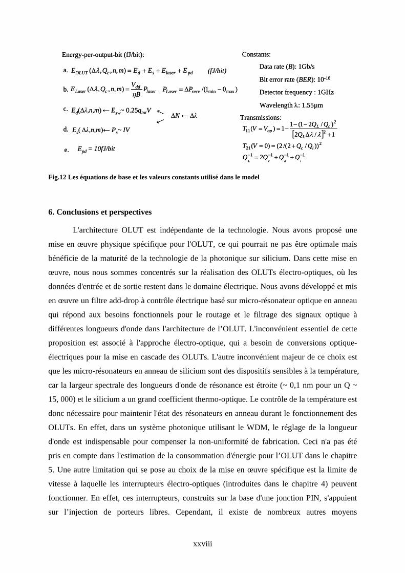
Ici, nous examinons les principes de base pour re-clarifier la relation entre les
paramètres décrivant les filtres add-drop, et la consommation d'énergie pour l’OLUT, basée
sur l'effet électro-optique. Les équations et les valeurs constantes utilisées par le modèle sont
présentées dans la Fig.12. Nous rappelons ici que la consommation globale d'énergie de
l’OLUT EOLUT (i.e. energy-per-output-bit, donnée par l’équation (a) sur la figure) est la
somme des contributions suivantes:
i) Ed (cf. Equation (4.17)) représente l'énergie dynamique dissipée par les filtres add-
drop pour effectuer la transition d'état (Drop to Through), qui doit injecter des porteurs
pour régler la longueur d'onde de résonance;
ii) Es (cf. Equation (4.18)) représente l'énergie statique consommée par les filtres add-
drop et est déterminée par la polarisation électrique et le courant obtenu selon la
simulation électrique de la jonction PIN du résonateur micro-anneau en silicium;
iii) Elaser (cf. Equation (4.19)) représente la puissance optique minimum d'entrée
délivrée par le laser pour distinguer le niveau logique « 1 » du niveau logique « 0 »
(selon la dissipation de l'énergie laser dans la OLUT) pour atteindre un taux d'erreur
par bit acceptable (BER=10-18 est choisie ici).
iv) Epd est une estimation de l'énergie dissipée par chaque photodétecteur et est
quantifiée à 10fJ/bit pour une fréquence de 1 GHz
Comme indiqué précédemment, les paramètres nécessaires pour décrire complètement
l’opération d’un filtre add-drop sont : le facteur de qualité de couplage Qc ; le décalage en
longueur d’onde ∆λ entre la longueur d'onde de résonance et la longueur d’onde du signal
d’entrée ; et le facteur de qualité intrinsèque Qi. Comme Qi est généralement fixé pour une
technologie donnée et pour un rayon d'anneau donné, les transmissions du filtre add-drop dans
le régime actif sont ainsi exprimées selon les valeurs de Qc et ∆λ. De ce fait, on peut
construire l'espace de conception possible sur la base des valeurs du facteur de qualité de
couplage Qc, ainsi que du décalage de longueur d'onde ∆λ. Pour un nombre de bits d'entrée
donné n, et un nombre de bits de sortie donné m:
• Des valeurs plus élevées de Ed et Es sont nécessaires pour le fonctionnement du n-m-
OLUT pour un décalage en longueur d'onde ∆λ plus élevé, parce qu'il y a plus de
porteurs libres à injecter. Toutefois, les valeurs de Ed et Es sont indépendantes de Qc

xxvii
• Cependant, Elaser est inversement proportionnelle à la différence minimale entre les
valeurs de transmission pire cas pour les niveaux logiques « 1 » et « 0 » (1min and 0max
dans l'équation (b) dans la Fig.12) et s’appuie donc sur les valeurs de Qc et de ∆λ.
D'une part, pour un plus grand décalage en longueur d'onde ∆λ, une valeur élevée de
transmission sera généralement obtenue au port Through du filtre add-drop dans l'état
Through, facilitant ainsi la distinction des niveaux logiques «1» et « 0 », ce qui devrait
conduire à une valeur plus faible de Elaser , à utiliser pour les OLUTs. D'autre part,
comme indiqué par les expressions de transmission dans la Fig.12, pour une valeur
plus grande de Qc (ou plus précisément du rapport Qc/Qi), il est plus difficile
d'atteindre l'état Drop lorsque le filtre add-drop est éteint (puisque T12 devient plus
faible), mais il n'aide pas à atteindre l'état Through (où T11 augmente) car une
augmentation Qc conduit à une réduction de la largeur spectrale de la résonance. Ceci
implique que l'impact de la valeur de Qc sur celle de Elaser n'est pas toujours le même
et dépend de l'état du filtre add-drop (Drop ou Through), car c'est celui-ci qui
déterminera essentiellement la valeur de transmission dans le pire cas. Par exemple, si
la transmission dans l'état Through est inférieure que dans l'état-Drop, une valeur
inférieure de Elaser est nécessaire pour augmenter Qc. Inversement, Elaser augmente
avec Qc lorsque la transmission de l'état Through est plus élevée que celle de l'état
Drop.
Pour résumer brièvement, pour une technologie donnée et un rayon d'anneau fixe (Qi
constant), l'énergie dissipée dans l'OLUT (EOLUT) repose essentiellement sur les valeurs du
facteur de qualité de couplage Qc et le décalage en longueur d'onde ∆λ. La valeur optimale de
Eolut peut être réalisée à partir d'un compromis entre la dissipation de l'énergie des lasers et les
filtres add-drop, pour différentes valeurs de Qc et ∆λ. Pour étudier les rapports entre la
dissipation d'énergie et ces paramètres physiques et ainsi obtenir la valeur minimale de Eolut,
nous présentons le calcul de l'espace de conception possible du Qc et ∆λ pour l'architecture
d’une 2-2-OLUT dans la figure 12.
xxviii
pdlasersdcOLUT EEEEmnQE +++=∆ ),,,( λ
laserdd
cLaser PB
VmnQEη
λ =∆ ),,,(
a.
b. )01/( maxmin −∆= recvLaser PP
c. Vqtot25.0Ed(∆λ,n,m)← Esw~
Es( ∆λ,n,m)← Ps~ IV
∆N ← ∆λ←←
d.
Constants:Energy-per-output-bit (fJ/bit):
Data rate (B): 1Gb/s
Bit error rate (BER): 10-18
Epd = 10fJ/bite.
(fJ/bit)
Wavelength λ: 1.55µm
Detector frequency : 1GHz
[ ]
1111
221
2
2
11
2
))/2/(2()0(
1/2)/21(1
1)(
−−−− ++=
+==
+∆
−−−==
iacLQQQQ
QQVT
QQQVVT
ic
L
cLop
λλ
Transmissions:
Fig.12 Les équations de base et les valeurs constants utilisé dans le model
6. Conclusions et perspectives
L'architecture OLUT est indépendante de la technologie. Nous avons proposé une
mise en œuvre physique spécifique pour l'OLUT, ce qui pourrait ne pas être optimale mais
bénéficie de la maturité de la technologie de la photonique sur silicium. Dans cette mise en
œuvre, nous nous sommes concentrés sur la réalisation des OLUTs électro-optiques, où les
données d'entrée et de sortie restent dans le domaine électrique. Nous avons développé et mis
en œuvre un filtre add-drop à contrôle électrique basé sur micro-résonateur optique en anneau
qui répond aux besoins fonctionnels pour le routage et le filtrage des signaux optique à
différentes longueurs d'onde dans l'architecture de l’OLUT. L'inconvénient essentiel de cette
proposition est associé à l'approche électro-optique, qui a besoin de conversions optique-
électriques pour la mise en cascade des OLUTs. L'autre inconvénient majeur de ce choix est
que les micro-résonateurs en anneau de silicium sont des dispositifs sensibles à la température,
car la largeur spectrale des longueurs d'onde de résonance est étroite (~ 0,1 nm pour un Q ~
15, 000) et le silicium a un grand coefficient thermo-optique. Le contrôle de la température est
donc nécessaire pour maintenir l'état des résonateurs en anneau durant le fonctionnement des
OLUTs. En effet, dans un système photonique utilisant le WDM, le réglage de la longueur
d'onde est indispensable pour compenser la non-uniformité de fabrication. Ceci n'a pas été
pris en compte dans l'estimation de la consommation d'énergie pour l’OLUT dans le chapitre
5. Une autre limitation qui se pose au choix de la mise en œuvre spécifique est la limite de
vitesse à laquelle les interrupteurs électro-optiques (introduites dans le chapitre 4) peuvent
fonctionner. En effet, ces interrupteurs, construits sur la base d'une jonction PIN, s'appuient
sur l’injection de porteurs libres. Cependant, il existe de nombreux autres moyens
xxix
d’implémenter le filtre add-drop : par exemple le coupleur directionnel, les cristaux
photoniques ou l'interféromètre Mach-Zehnder. En plus, en considérant les progrès de la
technologie, des composants plus compacts et plus économes en énergie deviennent
disponibles. Il est à noter que la frontière de la photonique sur silicium évolue extrêmement
rapidement avec de nouveaux dispositifs intégrés reportés chaque année. Cependant, notre
travail de modélisation ne repose pas sur des nouvelles contributions dans les performances
du dispositif (vitesse, puissance ou efficacité). Au lieu de cela, nous nous sommes concentrés
sur l'étude de la façon dont certains dispositifs photoniques sur silicium devraient être conçus
pour l'architecture de calcul pour atteindre les exigences de performance au niveau du
système. Dans ce contexte, nous avons également proposé une approche de modélisation
multi-niveau basée sur l'exploration de l’espace de conception et des paramètres de
composant pour estimer la performance du système. Cette méthode nous permet d'étudier la
faisabilité de l'architecture OLUT et d'explorer l'espace de conception de dispositifs
photoniques pour réaliser des calculs fiables et efficaces dans les architectures OLUTs. Cette
méthode pourrait donc être étendue à l'évaluation de la performance des OLUTs s’appuyant
sur différentes implémentations physiques, simplement en changeant le modèle physique
utilisé au niveau de composant.
L'évaluation des performances pour les architectures de l'OLUT électro-optique a été
présentée en utilisant l'approche de modélisation multi-niveau et le modèle physique.
L'impact des dimensions d'entrée d’OLUT sur les paramètres des composants, et par
conséquent sur l'efficacité énergétique du système, est étudié par le calcul de l'espace de
conception possible pour les OLUTs. Les résultats analytiques ont montré le potentiel des
architectures de OLUT d'accéder au dessous de 100 fJ/opération logique, ce qui est en effet
comparable à la dissipation totale d'énergie par l’opération logique pour les dispositifs actuels
de CMOS en silicium (au niveau du femto Joule, selon ITRS [5]). En outre, nous avons
illustré le potentiel de l'architecture n-m×2-OLUT pour améliorer l'efficacité du matériel et de
l'énergie par rapport à la n-m-OLUT en utilisant la mise en œuvre d'une unité logique
arithmétique 1-bit (ALU). Les résultats d'analyse ont mis en évidence l'avantage clé des
sorties complémentaires pour augmenter la capacité de calcul d'une OLUT jusqu'à 100%,
avec un surcoût raisonnable sur la puissance du laser optique d'entrée et de la surface du
système. Cependant, il est bien de souligner que le modèle proposé n’inclut pas certaines
sources de dissipation d'énergie, qui devraient être pris en compte dans un environnement réel.
Il s'agit par exemple de la consommation d'énergie statique pour les lasers, de l'énergie
xxx
requise par les filtres add-drop de pré-calibration en temps réel et de réglage thermique. Ces
points feront l'objet de sujets de travail futur.
Pour compléter les perspectives de ce travail de thèse, nous avons proposé une version plus
avancée de l'OLUT pour compenser les faiblesses associées à la mise en cascade des OLUTs,
grâce à l'utilisation d'un filtre add-drop tout-optique. L'interface tout-optique proposée permet
de cascader plusieurs OLUTs ensemble pour construire éventuellement une architecture
FPGA tout-optique, éliminant ainsi la latence et la consommation d'énergie associée avec des
interfaces opto-électriques. Cette approche permettrait également de bénéficier de vitesses de
calcul potentiellement plus élevées, car le filtre add-drop tout-optique a un débit bien plus
élevés que celui des dispositifs électro-optiques introduits dans le chapitre 4.

xxxi
TABLE OF CONTENTS
REMERCIEMENTS ............................................................................................ I
ABSTRACT ..................................................................................................... VII
RESUME FRANCAIS ...................................................................................... IX
CHAPTER 1 INTRODUCTION ................................................................... 1 1.1 Background ...................................................................................................... 1 1.2 Lesson from the history of optical computing ................................................. 6
1.2.1 Early days of optical computing ......................................................................... 6 1.2.2 Golden Age of optical computing ....................................................................... 7 1.2.3 Lessons and observations ................................................................................... 8
1.3 Optics in computing: what next? ................................................................... 11 1.4 Objectives and thesis outline .......................................................................... 14
CHAPTER 2 EMERGING TECHNOLOGIES FOR RECONFIGURABLE COMPUTING ............................................................ 17
2.1 Emerging technologies for reconfigurable computing architectures ............. 17 2.1.1 Introduction to computing architectures .......................................................... 17 2.1.2 FPGA Overview ............................................................................................... 19 2.1.3 FPGAs challenges and emerging technologies ................................................ 21
2.1.3.1 Non-volatile nano-memory devices ............................................................. 22 2.1.3.2 3D technology .............................................................................................. 25 2.1.3.3 Optical technologies for reconfigurable computing ..................................... 27
2.2 State-of-the-art: Silicon photonics based computing architectures ............... 29 2.2.1 Background ...................................................................................................... 29 2.2.2 Directed Logic .................................................................................................. 29 2.2.3 Reconfigurable Directed Logic ........................................................................ 31
2.3 Conclusions .................................................................................................... 35
CHAPTER 3 OLUT ARCHITECTURE DESIGN AND IMPLEMENTATION ....................................................................................... 37
3.1 Single-output OLUT Architecture ................................................................. 37 3.1.1 From electrical LUTs to optical LUTs ............................................................. 37 3.1.2 Basic principle and switching operation .......................................................... 38
3.2 n-m-OLUT architecture ................................................................................. 40 3.2.1 Operation principles ........................................................................................ 40 3.2.2 Preliminary evaluation of n-m-OLUTs ............................................................ 43
3.2.2.1 Evaluation Metrics ....................................................................................... 43 3.2.2.2 Scalability of OLUT architecture ................................................................. 45 3.2.2.3 Case study: k-bit full adder with carry ......................................................... 46
3.3 n-m×2-OLUT Architecture.............................................................................. 49 3.3.1 OLUT with Complementary Logic Output ....................................................... 49 3.3.2 Filtering Scheme in the complementary part ................................................... 52
xxxii
3.4 Conclusions .................................................................................................... 52
CHAPTER 4 FROM ARCHITECTURE TO DEVICE: MULTI-LEVEL MODELLING AND SIMULATION ............................................................... 55
4.1 Functional toolbox based on silicon photonics for implementing OLUT ..... 56 4.1.1 Passive Add-Drop Filters (Microring resonator) ............................................ 56
4.1.1.1 Basic Principles ............................................................................................ 56 4.1.1.2 Passive add-drop filter transmission and Coupled Mode Theory ................ 58
4.1.2 Silicon waveguides, integrated photodetectors and micro-lasers .................... 63 4.2 Design of active add-drop filters for OLUT architectures ............................. 65
4.2.1 Electrically-controlled modulation of an optical signal .................................. 65 4.2.1.1 Electro-optic effect ....................................................................................... 66 4.2.1.2 Thermo-optic effect ...................................................................................... 66 4.2.1.3 Free carrier dispersion and electro-refractive effect .................................... 68
4.2.2 Carrier electrical manipulation with PIN junction .......................................... 70 4.2.3 From the OLUT system dimension to the device building block geometry ...... 73 4.2.4 Transmission characteristics of the active Add-drop filter .............................. 74 4.2.5 Calculation of electrical control and power consumption ............................... 77 4.2.6 Speed consideration for electro-refractive add-drop filters ............................ 78
4.3 Multi-level modelling of OLUT and impact on the low level design of the OLUT building blocks .............................................................................................. 78
4.3.1 Overview of the multi-level modeling methodology ......................................... 79 4.3.2 Optical losses in OLUT architectures .............................................................. 80 4.3.3 OLUT energy model ......................................................................................... 83
4.3.3.1 Dynamic Energy Ed ..................................................................................... 84 4.3.3.2 Static Energy Es ........................................................................................... 85 4.3.3.3 Energy dissipated by the photodetectors Epd ............................................... 86 4.3.3.4 Energy dissipated by the laser Elaser ............................................................. 86
4.4 Conclusions .................................................................................................... 88
CHAPTER 5 PERFORMANCE EVALUATION OF THE ELECTRO-OPTIC OLUT IMPLEMENTATION ............................................................. 91
5.1 Case study and result analysis for n-m-OLUTs ............................................. 91 5.1.1 A review of the energy model introduced in chapter 4 .................................... 91 5.1.2 Feasible design space for the 2-2-OLUT ......................................................... 93 5.1.3 From 2 to m output bits .................................................................................... 99
5.1.3.1 Scalability and energy efficiency ................................................................. 99 5.1.3.2 Case study: 1-bit Arithmetic Logic Unit (ALU) ........................................ 102
5.1.4 From 2 to n input bits ..................................................................................... 102 5.2 Performance evaluation for the n-mx2-OLUT Architecture ......................... 105
5.2.1 Feasible design space for the 2-2 x2-OLUT .................................................... 105 5.2.2 Area and optical power overhead .................................................................. 106 5.2.3 Case study: a 1-bit ALU implemented by a n-mx2-OLUT .............................. 107
5.3 Conclusions .................................................................................................. 109
CHAPTER 6 CONCLUSIONS AND PERSPECTIVES ......................... 111 6.1 Conclusions .................................................................................................. 111
xxxiii
6.2 A possible all-optical implementation of OLUTs: towards all-optical FPGAs 116
6.2.1 Cascading of OLUTs ...................................................................................... 116 6.2.2 Interconnect network ...................................................................................... 119
6.2.2.1 ORNoC ....................................................................................................... 119 6.2.2.2 λ-router ....................................................................................................... 120
6.2.3 Case study: 4-bit full adder ............................................................................ 121 6.2.4 Discussion ...................................................................................................... 123
REFERENCES ................................................................................................ 125
APPENDIX ...................................................................................................... 139

xxxiv

xxxv
LIST OF ACRONYMS A
ALU Arithmetic Logic Unit
ASIC Application Specific Integrated Circuit
C
CLB Configurable Logic Block
CMOS Complementary Metal Oxide Semiconductor
CMT Coupled Mode Theory
CW Continuous Wave
E
EDA Electronic Design Automation
F
FDTD Finite Difference Time Domain
FSR Free Spectral Range
FPGA Fidel Programmable Gate Array
G
GPP General-Purpose processor
I
InP Indium Phosphide
L
LUT Look Up Table

xxxvi
O
OLUT Optical LookUp Table
ONoC Optical Network On Chip
R
RAM Random Access Memory
S
SOA Semiconductor Optical Amplifier
SOI Silicon On Insulator
T
TSV Through-Silicon-Via
V
VCSEL Vertical Cavity Surface-Emitting Laser
W
WDM Wavelength Division Multiplexing

Chapter 1 Introduction 1
Chapter 1 INTRODUCTION
1.1 Background
Today’s era of high-performance computing and big data analysis promises to bring
profound and far-reaching changes to society [1]. These changes are made at all levels of
information systems – from data acquisition in distributed sensor networks to storage and
processing in the cloud. Many computationally demanding applications, e.g. social network
analysis, quantum physics simulation, weather forecasting, disaster prediction, oil and gas
exploration, molecular simulation, increasingly require high-performance, cost-effective,
energy-economic computing hardware [3]. However, these constraints are conflicting in
conventional or incremental computing systems, and have also proved to be a major challenge
in disruptive approaches. New computing paradigms are thus required to address the energy
and performance challenges of computing in the data explosion era.
In the past, advances in semiconductor technology have been the main vehicle for
expanding the boundaries of computing. The long-term trend in semiconductor technology
was famously predicted in a paper by Gordon Moore in 1965 [4], in which he observed that
the number of electronic transistors that could be fabricated in an integrated circuit (IC) would
approximately double every year (later, the time between technology generations was
extended to two years). Circuit miniaturization through down-scaling of the critical
dimensions of transistors has thus been the primary driving force for the increase in the
microprocessor computational power. Following Moore's law for almost five decades, today's
microprocessors have already broken the billion transistor barrier. The ITRS Semiconductor
roadmap [5] shows yet further reductions in transistor feature sizes from 22nm down to the
sub-10nm regime in the next decade.
However, the scaling of physical dimensions and device speed are now mainly limited
by energy dissipation [7]. According to the physical laws such as Heisenberg uncertainty
principle and Landauer rule (the minimum energy required to generate a bit of information
is 2lnKT , where K is the Boltzmann constant and T is the temperature in Kelvin), the
maximum operation frequency of a switch is 25x1012 Hz. If the device operates at this
frequency, the resulting integrated circuit would consume more than 4x10⁶ W/cm2. The heat
generated would thus vaporize the circuit immediately once it is turned on [7]. Moreover, not
Chapter 1 Introduction 2
only does clock frequency appear to be limited, but also memory performance improvement
has not kept pace with processor performance scaling. The mismatch between memory
read/write speed and computational speed presents a wall to the scaling of overall
computational performance in CMOS technology. To address these issues, the computing
architecture has been shifted from a single microprocessor to multi-core (parallelism-driven)
processor architectures. Computing parallelism has been exploited by using more CPUs and
processing units, data/instruction parallel execution units, additional register sets, more cache
and heterogeneous processors (e.g. Graphic Processing Units) [3,6] on the chip. Such a shift
from sequential to parallel computer architecture would help to increase performance and
robustness while keeping power consumption relatively constant. However, parallel
computing architectures have to face new challenges compared to single processor
architectures. A critical issue is the energy dissipated by the interconnect required to realize
high-speed data communications between various computing resources in the multi-core
computing system. Although its computing performance could scale with the growing number
of cores, the electrical interconnects increasingly present a bottleneck due to their physical
limitations in terms of loss, dispersion, cross-talk and bandwidth [1-3,7,12,13]. It therefore
becomes very difficult to improve the computing performance when interconnect densities
continue to rise. For instance, a total interconnect data rate of 50-100 TBit/s in future multi-
core chips is expected by 2015 and more than the double of that by 2022, with a maximum
average allowed data communication energy dissipated on a chip ranging from 0.1 to 1pJ/bit
[13]. In high-density electrical interconnect, because the time constant of electrical wires
increases as device dimensions are scaled down, the energy costs for transporting information
electrically can be extremely high. From [8], the projected energy cost of off-chip electrical
communication is expected to be 5.8 pJ/bit in 2017 while the current practice reaches about
20 pJ/bit. At this cost, therefore, most of the available power will be consumed to move data
between processors and off-chip computing resources. Yet, as we demand more from the
computing architectures, even such parallel computing systems will be increasingly energy-
constrained. Therefore, producing computing systems that meet the performance, energy and
communication demands of emerging applications will likely be impossible.
As a result, to improve the energy efficiency of the computing system, emerging
technologies are urgently needed, such as silicon photonics, three-dimensional integration,
emerging memories and near-threshold voltage etc. In particular, optical cables have been
considered as a viable alternative to copper interconnect for transferring information between

Chapter 1 Introduction 3
computing elements and systems, and can potentially help the intrinsic limitations of
electrical interconnects to be overcome [16]. As witnessed from the telecommunication
industry with mature optical fiber technology, optics has already proved to be the best
technology for conveying information from one point to another over long distance. In 2013,
US National Research Council published a report on the advantages of photonics [8], which
wrote: “The remarkable growth of networks and the Internet over the past decade has been
enabled by previous generations of optical technology. Optics is, furthermore, the only
technology with the physical headroom to keep up with this exponentially growing demand
for communicating information”. The fact that light can be easily transmitted in parallel in
free space or in a guiding medium, with very low crosstalk, is of great importance.
Fig.1 summarizes the evolution in optical interconnects observed by [9]. The past two
decades have witnessed milestones of single-mode fibers in replacing telephone lines as the
primary mechanism for transmitting data over medium to long distances (WAN, LAN),
mostly thanks to the extraordinary growth of the Internet and network traffic. From 1998
when Harnessing light [14] was published to today, the capacity per wavelength in
commercial WDM long-distance networks has increased from a maximum of 10 Gb/s per
wavelength to more than 100Gb/s [8]. In addition, with increasing bandwidth demands,
optical technology is increasingly used in short-distance data communication within local
networks for high-performance computing systems [10], such as data centers, clustered
supercomputers and storage area networks (specifically for distance from several kilometers
down to less than 100 meters). Considering that low cost is particularly critical for short-reach
applications, technologies such as VCSEL laser arrays and multimode fibers (rather than
single-mode fibers and DFB lasers) are becoming widely employed [8] [11].
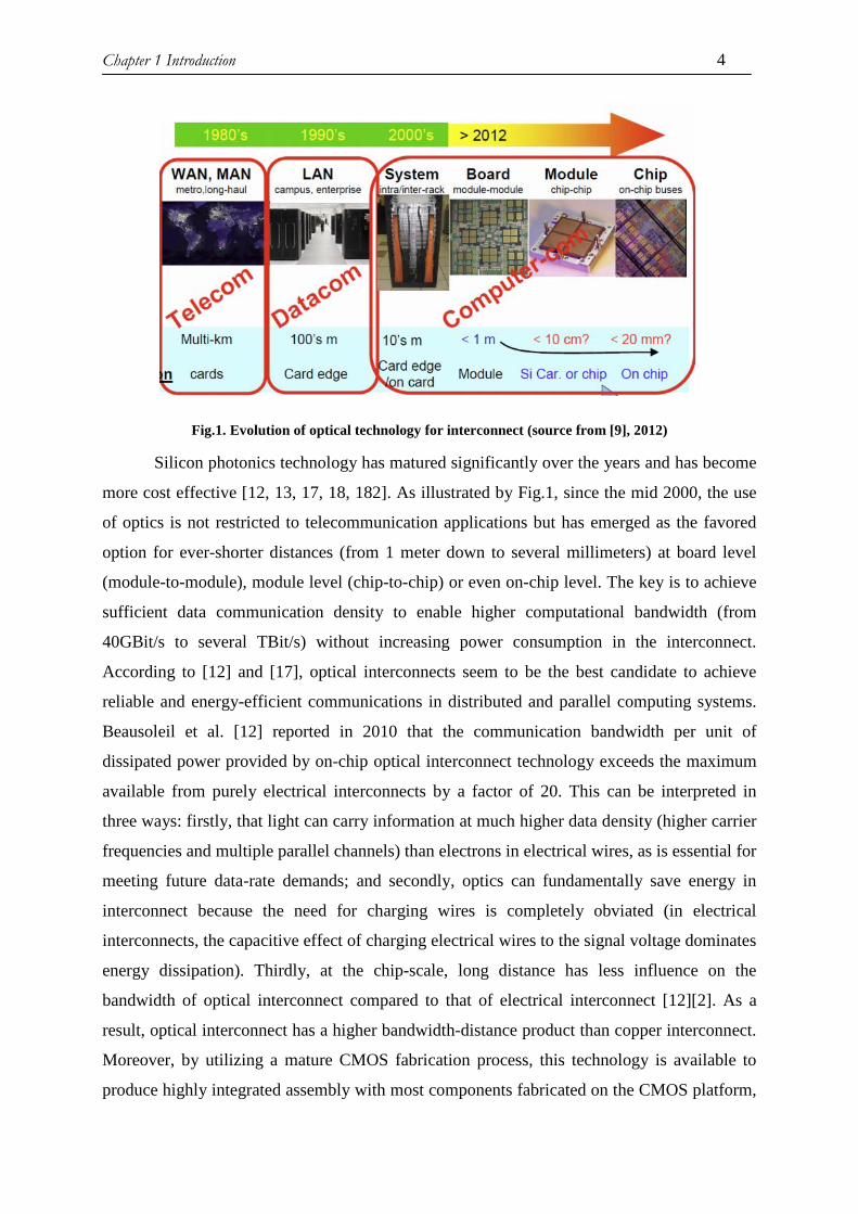
Chapter 1 Introduction 4
Fig.1. Evolution of optical technology for interconnect (source from [9], 2012)
Silicon photonics technology has matured significantly over the years and has become
more cost effective [12, 13, 17, 18, 182]. As illustrated by Fig.1, since the mid 2000, the use
of optics is not restricted to telecommunication applications but has emerged as the favored
option for ever-shorter distances (from 1 meter down to several millimeters) at board level
(module-to-module), module level (chip-to-chip) or even on-chip level. The key is to achieve
sufficient data communication density to enable higher computational bandwidth (from
40GBit/s to several TBit/s) without increasing power consumption in the interconnect.
According to [12] and [17], optical interconnects seem to be the best candidate to achieve
reliable and energy-efficient communications in distributed and parallel computing systems.
Beausoleil et al. [12] reported in 2010 that the communication bandwidth per unit of
dissipated power provided by on-chip optical interconnect technology exceeds the maximum
available from purely electrical interconnects by a factor of 20. This can be interpreted in
three ways: firstly, that light can carry information at much higher data density (higher carrier
frequencies and multiple parallel channels) than electrons in electrical wires, as is essential for
meeting future data-rate demands; and secondly, optics can fundamentally save energy in
interconnect because the need for charging wires is completely obviated (in electrical
interconnects, the capacitive effect of charging electrical wires to the signal voltage dominates
energy dissipation). Thirdly, at the chip-scale, long distance has less influence on the
bandwidth of optical interconnect compared to that of electrical interconnect [12][2]. As a
result, optical interconnect has a higher bandwidth-distance product than copper interconnect.
Moreover, by utilizing a mature CMOS fabrication process, this technology is available to
produce highly integrated assembly with most components fabricated on the CMOS platform,

Chapter 1 Introduction 5
thus greatly reducing the manufacturing cost. Numerous research efforts have focused on
optical interconnects based on silicon photonics (or optical network-on-chip, ONoC) to prove
its feasibility and benefits over electrical interconnects (THz bandwidth, low power, low loss
and low crosstalk). Several projects targeting high performance computing systems based on
photonic interconnect have been launched by industrial companies such as Intel, IBM, Oracle,
HP and Avago since 2009. However, the key challenges for on-chip optical interconnect are
technological: CMOS compatible, low energy dissipation and high performance compact
novel optical devices are required to be integrated at a large scale with low manufacturing
cost, as pointed out by Miller[13] in 2009.
Today optics is likely to be very successful for on-chip interconnect/communication in
computing systems [5,17-20]. But optical technology is believed to hold the promise to go
beyond realizing communication channels or networks for ultrafast massive data transmission,
and could also be exploited to perform digital computation in an all-optical way as well. This
can potentially lead to an additional increase in speed, bandwidth and energy efficiency as
compared to transistors based computations in electrical domain. Such idea of using optics for
computing as a replacement to electronics has attracted attention for more than half a century
but has never becomes reality. This has been recognized by most experts in the field.
Caulfield wrote in his paper on the perspectives of optical computing in 1998 as follows [31]:
“The only way for optical practitioners to win the “war” with electronics is to abandon it”.
He described the evolution of viewing optics over electronics in computing: the first phrase is
the “ignorance and underestimation” of electronics then “awakening and fear of inferiority”
and now “realistic acceptance that optical computing and electronics are eternal partners”.
But he also pointed that optics could do useful things electronics cannot and it is worth
exploring what roles optics is best at. In 2010, he wrote another paper investigating the
requirement of optics in future supercomputing, where he pointed out that the potential of
optics for computing particularly lies in parallel real-time information processing and the
future of optics might be the use of nanotechnologies. However, since the origin of optical
computing research in early 50s, there have always been many doubts about the potential of
optics for computing [52]. The reasons are various and worth to be investigated. Therefore, by
reviewing the historic evolution of optical computing, we investigate in the next section why
optical computing could not compete with electronic over the past few decades, where the
limitations are and conversely what can be hoped for.
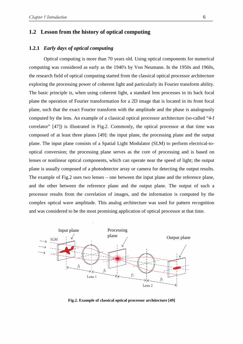
Chapter 1 Introduction 6
1.2 Lesson from the history of optical computing
1.2.1 Early days of optical computing
Optical computing is more than 70 years old. Using optical components for numerical
computing was considered as early as the 1940's by Von Neumann. In the 1950s and 1960s,
the research field of optical computing started from the classical optical processor architecture
exploring the processing power of coherent light and particularly its Fourier transform ability.
The basic principle is, when using coherent light, a standard lens processes in its back focal
plane the operation of Fourier transformation for a 2D image that is located in its front focal
plane, such that the exact Fourier transform with the amplitude and the phase is analogously
computed by the lens. An example of a classical optical processor architecture (so-called “4-f
correlator” [47]) is illustrated in Fig.2. Commonly, the optical processor at that time was
composed of at least three planes [49]: the input plane, the processing plane and the output
plane. The input plane consists of a Spatial Light Modulator (SLM) to perform electrical-to-
optical conversion; the processing plane serves as the core of processing and is based on
lenses or nonlinear optical components, which can operate near the speed of light; the output
plane is usually composed of a photodetector array or camera for detecting the output results.
The example of Fig.2 uses two lenses – one between the input plane and the reference plane,
and the other between the reference plane and the output plane. The output of such a
processor results from the correlation of images, and the information is computed by the
complex optical wave amplitude. This analog architecture was used for pattern recognition
and was considered to be the most promising application of optical processor at that time.
Input plane Processing plane Output plane
Input plane Processing plane Output plane
Fig.2. Example of classical optical processor architecture [49]

Chapter 1 Introduction 7
Since holography was invented by Gabor in 1948 [28], research development in the
field of optical computing was limited until the invention of the laser as a coherent light
source in 1960 [50], which then led to rapid progress in the design of optical correlator
architectures for real-time information processing. Coherent processor architectures like the
joint Fourier transform correlator were presented (e.g. by Goodman [48]), as well as
incoherent architectures to compute information through wave intensities for character
recognition [51]. However, due to the poor performance and high cost of critical components
such as the SLM, the advancement of optical processing was slow [14]. At the beginning of
the 1970s, rapidly developing digital electronic computers were demonstrated to compete
successfully with coherent optical computers for specific defense applications, such as the
processing of synthetic aperture radar data [52]. Without major showstoppers, the path to
higher performance computing with electronics was clear, and massive investments in this
sector led to significantly cheaper and more mature solutions than optics in most of
computing applications. However, the first years of optical computing still generated much
enthusiasm concerning the potential of optics for information processing, in specific domains.
In 1962, researchers at a symposium on optical processing [52] recognized that “special-
purpose optical processors could be used in the fields of pattern recognition and information
retrieval since optical systems offer in these cases the ability to process many items in parallel,
while the generous-purpose optical processors were questioned”. It was recognized that
optical technology was not ready to compete with electronic computing and that perhaps
optical computers would have a different form than electronic ones. Several decades after that
conference, it is of course clear that the general-purpose optical computer has not appeared,
and even optical correlators for pattern recognition have almost disappeared due to its size
and lack of accuracy.
1.2.2 Golden Age of optical computing
Fortunately, the slowdown period was then followed by a so-called “golden age” of
optical computing from the 1980s to 2000s [15]. Although no longer directly in competition
with electronic computing, the generated research results in optical computing have
contributed strongly to the development of new research topics such as biophotonics,
nanophotonics, optofluidics, and femtosecond nonlinear optics. In this period, remarkable
progress was made in specific research topics of optical computing such as pattern
recognition and optical memories. Various analog processors were constructed by taking

Chapter 1 Introduction 8
advantage of technological advancement in SLMs, optical filters and analog optical processor
architectures. Most of these processors remained at laboratories, but some were tested for
real-time applications. For example, in 1982, Cleland et al. [38] developed an optical
processor for detecting signal tracks based on a matrix of LEDs as the input plane, and was
also evaluated in a high-energy physics experiment in Brookhaven. In 1986, Ambs et al.
implemented an optical processor based on a matrix of 256×256 optically recorded holograms
[39]. A prototype of a correlator processor compliant with the PCI (Peripheral Component
Interconnect) interface, which can be used for processing video data at 65MB/s, was also
constructed [40]. In addition, optical processors were designed for many other information
processing applications such as matrix operations [41], systolic array processing [42] and
neural networks [43].
To become commercially feasible and to compete with electronic computing in
specific applications, research effort has focused on moving from analog optical processors to
digital optical processors. Thanks to the invention of vertical-cavity surface-emitting lasers
(VCSELs) in the early 1990s, several digital optical computer architectures were
demonstrated. For instance, sponsored by the Naval Research Office and NASA, Stone et al.
proposed a 32-bit fully-programmable digital optical computer (DOC II) designed to operate
in a UNIX environment and run basic RISC microcode [45]. The system is based on laser
diode arrays, multichannel SLMs, and avalanche photodiode arrays. By using data input in a
dual rail format, parallel microcode implementation was achieved, including an architectural
balance of optical interconnect and software code efficiency. Rudokas et al. demonstrated a
programmable optical digital ALU by implementing some RISC instructions on DOC II,
demonstrating gate interconnect bandwidth products (GIBPs) of up to 1016 with power
consumption of the order of 100W [46]. However, optical processors still have no solution to
tackle computing science issues such as complexity, accuracy, decisions and reliability.
Indeed, electronics is far more mature and can do almost anything optics can do in digital
computing applications with much lower cost. Moreover, as highlighted by Caulfield and
other researchers [31], even in domains more naturally suited to optics, e.g. Fourier
transforms, electronic chips have overwhelmed optics in terms of throughput and accuracy.
1.2.3 Lessons and observations
Much can be learned from this lesson and some of the most important reasons behind
the predominance of electronics over optics for computing can be summarized as follows:

Chapter 1 Introduction 9
- The accuracy advantage of electronics results from its being digital. Arbitrary
accuracy can be achieved at the cost of breaking computation tasks into smaller tasks such
that error rates are minimized, and errors can be corrected with more computation. The use of
analog optical processors implies the use of a large, not-so-accurate computation system. In
addition, a digital computer is more flexible than an analog one - to change functionality,
analog hardware must be changed since there is no provision for hardware reconfiguration;
while changing functionality in a digital computer can be achieved by changing the
instruction inputs. Therefore, it is crucial to design reconfigurable optical computing
hardware which is flexible to evolve with the evolution of the computing applications.
- A common term used in reference of optical computing is “computing at the speed of
light.” Processing information by light can be faster than by electronics under some
circumstances, but there are limits to this. Firstly, according to [31] and [38], electronic
signals in copper wires and optical signals in guiding materials (e.g. fibers, silicon) have
approximately the same upper speed limit. We know that a closely spaced bundle of wires
suffers from some physical effects, such as capacitive coupling and electromagnetic
interference of electrical signals, which can dramatically reduce the transmission speed of
electrons by some orders of magnitude. However, closely spaced optical fibers (or optical
waveguides) lead to an even worse situation: information leaks between them within the
nominal numerical aperture of the fiber (or due to phase coherent energy transferring between
waveguides) [31], such that the received information is not the transmitted information. And
secondly, computational performance is obviously not measured in centimeters per second,
though the speed is one factor in performance of computing components. Indeed, in current
silicon CMOS transistors with ~20nm critical size, electron can travel at the speed in the pico-
second range with a future projection in the range of 100 femtosecond (considering that the
typical saturation velocity that can be reached by an electron is 1x107 cm/s [12]), which is
comparable to the internal propagation speed can be achieved by photon in an optical switch
(assuming a typical optical signal propagation length of tens of micrometers and the photons
travel at a speed close to ~ c/3 (c is the light speed in vacuum). The carrier velocity in
transistors definitely contributes to the device switching speed, as does the channel length of
transistors and the voltage applied across the transistor tunnel. While reducing the transistor
size reduces propagation delay at constant carrier speed and consequently increase the device
operating speed, the energy dissipated by transistors increase significantly. In contrast, the
only fundamental limit on the switching time of optical switching devices arises from the

Chapter 1 Introduction 10
energy-time uncertainty [153]. In principle, the switching energy consumption of an optical
switch can be as low as several hundred attojaules if the device operates at a very high speed
~c/3 (the switching time in a range of sub-picosecond). In particular, the switching time will
be accumulated for (larger) electronic circuits with more transistors in series, while it is non-
cumulative for larger photonic structures consisting of more optical switching elements, since
all these elements integrated in a photonic circuit can be driven simultaneously, thereby
potentially leading to low latency and high bandwidth.
- Lower interaction between photons makes it more difficult to construct switches
similar to electronic transistors (fundamentally two electrons cannot be in the same place at
the same time due to their strong interaction), which are the core component for computing.
Although a lot of research progresses were made in optical switches processing logical
operations using nonlinear optical effects [33], it is impossible in the foreseeable future that
optical devices can have a size roughly equal to that of the electronic switches, and most
importantly, optical switch would consume a lot more power for generating nonlinear effect
between photons and the material used. Moreover, a fundamental difference is that an
electronic switch will block the current flow, while an optical switch deviates the photon flow
to somewhere other than where the information will be detected. Whatever the state of the
optical switch, light is being generated and energy consumed. Also, optical memories that are
based on the storage of photons have been difficult to achieve, whereas electronic memories
rely on the simple storage of electrical charges on a capacitor. However, optics is still
potentially suitable to design switches in future. On the one hand, potential breakthrough may
be made with the technological advance of the materials with optical nonlinearities in the
coming yeas. On the other hand, the unique properties of light (e.g. light spectrum, phase,
and polarization) and the pulse-based representation of information, rather than levels
of light intensity, might play a beneficial role for computation. Furthermore, for non Von-
Neumann computing paradigms, e.g. neuromorphic computing, some fast optical nonlinear
effects can be used to design high speed switches with rich intrinsic dynamics and
consequently facilitate the neural behaviors in these systems [177].
- The featured advantage of optics over electronics for massive data transmission
comes from the fact that incoherent light beams do not interact with each other during
propagation, and each can behave independently in some respects. But it happens to be a
critical drawback for optical computing, since even the interference of two optical signals
takes place under specific conditions [153,151]. Therefore, writing information (like

Chapter 1 Introduction 11
bitstreams of data) onto the light beam commonly uses electronics - electro-optic modulators
and photodetectors explicitly serve at this role. Implicitly, even switching devices based on
nonlinear optics have to use electronics (i.e. carriers) for achieving much lower power
consumption than those use pure optics. Consequently, the physical conversion between
optics and electronics is a prerequisite component of optical computing systems. But
ironically, with the use of electronics, the overall performance of an optical computing system
is often limited by that of the input and output interfaces, which are commonly the slowest (i.e.
highest latency) and most energy consuming parts. In short, the limitations of the optical
computing systems are within the electronic interfaces, and it is therefore difficult to improve
the performance by directly replacing electronics with optics in the computing systems.
Therefore, the future optical computing architecture has to stay in the domain of optics as
much as possible and limit the usage of electro-optic interfaces.
1.3 Optics in computing: what next?
In light of these experiences, what now are the appropriate roles that optics can play
for information processing and what are the perspectives for optical computing? It would
appear clear that while it is illusory to consider that optics can directly compete with
electronics based computing, it can fill a useful role in niche functions to help computing
systems work better [31-34]. In terms of the different formats of the information that are
required to be processed:
- If the input and output information are in optical form (e.g. optical images), then
when performing operations such as correlation, convolution and optical Fourier
transformation in real-time image processing, optical approaches are favorable. In this
situation, electro-optical conversions are no longer needed. Moreover, there is no need to
force optics to behave as electronics in such systems, thereby taking advantage of the intrinsic
properties of light for achieving computation with potentially high bandwidth and low power
consumption.
- On the other hand, if the input and output data are non-optical, then it might be better
to associate optics with electronics to implement some functionalities that pure electronics is
less efficient at doing.
This can be interpreted as follows:
Chapter 1 Introduction 12
- Electronics commonly handles complexity in two ways: the use of space (e.g.
parallel buses, multi-cores) and time (e.g. pipelined datapaths), but optics has a third vector:
wavelength. Many independent light beams at different wavelengths can be modified,
commonly or independently, by a single control signal in an optical information processing
system. This is very promising to create highly-parallel powerful computing architectures.
Indeed, as we will discuss in the following chapters, the wavelength vector plays a
fundamental role in the reconfigurable photonic logic architecture proposed in this thesis.
Additionally, optical technology can implement massive, parallel, arbitrary mapping from an
NxN input array form to an N×N output array form using N weighted interconnections through
N wavelengths [31], where the phase of optical signals is critical for weighted
interconnections. Such a function can serve as the backbone of a massively parallel neural
network e.g. reservoir computing [177] [35]. Because of this, optics can be exploited to
perform parallel computation tasks for parallel computing architectures integrating massive
logic components.
- Optical computing may help to alleviate heat generation issues in electronic
processors. As mentioned before, the heat problem of electronic devices worsens as operation
speed increases and device geometry decreases: faster operations require more power, while
smaller devices occupy less area from which the resulting heat is more difficult to remove.
Optical systems, however, do not increase heat dissipation significantly as compared to
electronic chips when increasing the operation speed. This aspect has been demonstrated by
many computing systems based on optical network-on-chips (ONoCs).
- Digital computing systems do not handle continuous data well. It was once thought
that continuous-time computations could be approximated arbitrarily with current computing
systems. However, the study of chaos shows that this is not true, for example when using such
systems to manipulate continuous variables [37][14]. For example, it is possible to transform
a continuous-time function into the discrete-time domain using digital sampling and
transformation techniques, but it is impossible to perform continuous-time transformations on
continuous-time signals directly in the digital domain. In this case, analog techniques (i.e. in
the optical or electrical domains) are needed. Optics has the inherently continuous properties
defined by wave theory and wave equations, so optics might be favorable for solving this type
of problems. From this point of view, an analog optical processor could operate at a much
higher data rate than analog electronics in analog computing systems processing continuous
operation. This is seen from recent trends in designing optical reservoir computing systems
Chapter 1 Introduction 13
for carrying out the recognition tasks and generating continuous signals [177][35], which
typically use an interconnected array of nonlinear optical components.
- Power consumption is one of the main bottlenecks in current computing systems. In
electronic circuits, performing any logic operation consumes a finite (and small) amount of
energy. As a complex logic function is commonly decomposed into small sub-functions, a
great number of intermediate logic stages are necessary. These logic stages generate useless
logic data and lead to high energy dissipation. However, this could be avoided in an optical
computing system that generates results by the manipulation and the propagation of light. For
example, Directed Logic [34] (see section 2.2.2 for more details) has been recently proposed.
It performs logic operations by directly propagating a light beam through a network of
interconnected optical switches. Since the intermediate logics and their dissipated energy are
avoided, the total energy dissipation of the logic circuit could be potentially reduced.
- Finally, optical memories, i.e. holographic memories, seem to be very attractive for
being potentially high density and enabling parallel data access, as compared to conventional
memories [14]. Research in this aspect has been started from the early 1960s, which is
marked by the development of the theory of optical storage through using 3D materials [21].
Shortly after that, holographic memories using films such as synthetic holography has been
proposed for recording and storing digital data in the Human Read/Machine Read (HRMR)
system [23]. Rapid progress was made in the 1980s and 1990s in developing 3D parallel
access optical memory. For instance, Marchand et al. proposed a motionless-head parallel
readout optical-disk system with a maximum data rate of 1.2Gb/s [24]. In addition, there were
some start-up companies created for developing holographic memories but most of them
disappeared. One of them however has commercialized a holographic disk memory product
based on photopolymer material [27]. Today the holographic memory is still a candidate for
future memories. However, this choice is limited by the recording material, and particularly
by the fact that there is no explicit method to use cheap rewritable material [30].
We discussed here some roles in future computing systems that optics could be
suitable for. There are probably other roles that optics could play that electronics cannot, such
as zero-energy logic, or quantum computing etc. However, all these propositions are still in
the early stages of research and need to be investigated further.

Chapter 1 Introduction 14
1.4 Objectives and thesis outline
The work described in this thesis aims at the design of a new reconfigurable
computing architecture that can be implemented in a silicon photonic integrated circuit, so as
to address the energy, bandwidth and reconfiguration issues of conventional computing
architectures. This work lies in the context of optical computing but with a focus on on-chip
reconfigurable computing, at the boundary of computing system design and photonic device
modeling. The outline of this thesis is given as follows:
This chapter has given an introduction to the background of information processing
systems, including an overview of the technological challenges in electronic computing
systems and trends of using optical technology for on-chip communication. It then reviewed
the historical evolution of optical computing with a focus on the lessons and the reasons
behind the lack of success of optical computing. Finally, we summarized the roles that optics
could play in computing systems by analyzing some important features that optics has.
Chapter 2 reviews the various types of computing architectures and highlights the
major challenges in conventional reconfigurable computing architectures (e.g. FPGAs),
particularly the high power consumption and low computation capacity. It then discusses the
current trends of emerging technologies for implementing reconfigurable computing
architectures, such as 3D technology, emerging nano-memories and optical technologies. This
chapter then focuses on the state-of-the-art optical computing architectures. The analysis
shows that the optical approach can be used to implement reconfigurable computing systems
with the promise of reduced latency and energy dissipation.
Chapter 3 proposes a reconfigurable block based on silicon photonics, the optical look
up table (OLUT) and associated logic architectures. We start by introducing a basic OLUT
block that is equivalent with an electrical LUT. It then presents the OLUT with multiple
outputs by taking advantage of WDM for parallel computation, thereby resulting in higher
bandwidth, higher hardware efficiency and potentially lower energy consumption. The
operation principles and filtering schemes of OLUTs are investigated followed by a
preliminary performance evaluation of OLUTs through an example of a full-bit adder.
Progressively, we extend the initial OLUT architecture by proposing a complementary logic
output to simultaneously perform a pair of complementary logic functions, leading to higher
computational efficiency with reasonable hardware overhead.
Chapter 1 Introduction 15
Chapter 4 proposes one physical implementation of OLUTs. It is thus devoted to the
multilevel modeling of this OLUT architecture, including the physical-level design of its key
building block, i.e. an electrically controlled add-drop filter. It lays the foundation for the
system-level performance evaluation with a strong emphasis on the energy dissipation of
OLUTs. It offers an analysis of the transmission response of the add-drop filter in both
passive and active regimes through coupled mode theory and explores a range of electrically
controlled optical signal modulation schemes, focusing on carrier manipulation through a PIN
junction. It then subsequently analyzes the optical losses occurring in the photonic circuit
layout for the OLUT system. Finally, the complete energy model including the contribution of
all the active components in OLUT is described.
Chapter 5 presents the performance evaluation results for the OLUT architectures by
using the multi-level modeling approach and the energy model described in chapter 4. In the
fist part, the energy dissipation of the n-m-OLUT architecture is evaluated by calculating the
feasible design space for the parameters of add-drop filters. The impact of the input and
output dimensions of OLUT on its energy efficiency is well studied. Its second section
explores the OLUT with the complementary logic interface for further improving the
computation performance and energy efficiency of OLUT. The input optical laser power and
area cost for performing complementary logic computations in the n-mx2-OLUT architecture
is also analyzed.
Chapter 6 concludes the thesis and discusses the perspectives of the proposed OLUT
as a reconfigurable computing paradigm for the future. In particular, an all-optical OLUT
based on an all-optical input and output interface is proposed for the cascade of multiple
OLUTs.

Chapter 1 Introduction 16

Chapter 2 Emerging technologies for reconfigurable computing 17
Chapter 2 EMERGING TECHNOLOGIES FOR RECONFIGURABLE COMPUTING
This chapter reviews emerging technologies for implementing reconfigurable
computing architectures, with a focus on silicon photonics technology. Due to a variety of
reasons such as increased power consumption, heat generation and current leakage in
integrated circuits, the performance of microprocessors is no longer increasing exponentially.
Silicon photonics is considered as a potential solution to help microelectronic chips continue
to improve performance per unit energy ratios. Silicon photonics is already widely used for
optical interconnects and data communication in high-end computing systems, i.e. data
centers, networks etc. It also holds the promise for realizing on-chip reconfigurable
computing architectures.
The chapter is organized as follows. Section 2.1 first gives a brief introduction of the
FPGA architectures, and then discusses key challenges and solutions, including a survey of
some important trends to design future FPGAs. The potential benefits of emerging
technologies, such as low power consumption, low latency, low cost and high performance
are analyzed. Section 2.2 introduces the silicon photonics technology and shows the related
work that exploits it for implementing reconfigurable computing architectures.
2.1 Emerging technologies for reconfigurable computing architectures
2.1.1 Introduction to computing architectures
The computer architecture is the conceptualization of the fundamental operating
principles of a computing system [155]. It commonly considers how to use hardware
components and design the software to implement the computing systems that meet functional,
performance and cost targets. Three main architectural options are general-purpose processors,
application-specific integrated circuits (ASICs) and reconfigurable computing systems
(usually) based on field-programmable gate arrays (FPGAs). General purpose processors
(GPPs) execute sequentially a set of software instructions to perform a computing task. They
are applicable to most of the tasks thanks to their flexibility introduced by software
programming. However, since their hardware is not optimized for a specific application [156],
they are energy consuming and performance inefficient for many emerging tasks. Conversely,

Chapter 2 Emerging technologies for reconfigurable computing 18
ASICs are dedicated hardware devices that are specialized to a particular application. For a
given computing task, ASICs achieve better performance with lower power consumption and
less area utilization than GPPs. However, due to their fixed nature, ASICs cannot be
modified when the target application changes, such that, although it can offer the best
performance for a specific application, it cannot be used for other applications. Additionally,
an ASIC chip is considered to have higher non-recurring engineering costs, implying that
development is time-consuming and fabrication expensive [157]. Reconfigurable computing
offers an alternative architectural option to GPPs and ASICs by allowing its hardware
components (i.e. logic blocks and interconnects) to be configured and customized to suit a
specific computing task through post-fabrication and user-defined programming [54]. They
offer higher performance than GPPs while achieving a higher level of flexibility than ASICs.
For instance, a point multiplication with a key size of 270 bits can be computed in 0.36ms in a
reconfigurable system implemented in an XC2V6000 FPGA driven at 66MHz while an
optimized software implementation takes 196.71ms on a dual-Xeon computer driven at
2.6GHz [55]. This therefore demonstrates a 540x computation speed-up in reconfigurable
systems while its clock rate is almost 40 times slower than the microprocessor. The main
issue to be addressed for reconfigurable computing is that its flexibility comes at a higher cost
in speed, area and power consumption than the ASICs [55][59][62]. But the flexibility may
advantageously lead to a shorter time-to-market and lower non-recurring engineering costs,
thereby relaxing the budgetary and R&D constraints. This makes reconfigurable computing
systems a better alternative than ASICs for many applications in future network, computer,
data centers and communication systems. This trend has been recognized by researchers in the
“FPGAs in 2032” workshop in 2012. By reviewing the history of programmable devices over
the last 20 years and then extrapolating it for the next 20 years, they concluded: “in 2032,
every system-level device will have to be programmable: at run time, the chip will have to
configure its still-functioning resources into a working system.”[56]
To date, most reconfigurable computing architectures commonly rely on FPGAs as the
core processing unit. This will be introduced in the next section. We then discuss the
challenges of FPGAs and take a look at the emerging technologies for reconfigurable
computing.

Chapter 2 Emerging technologies for reconfigurable computing 19
2.1.2 FPGA Overview
FPGAs are prefabricated semiconductor chips that typically consist of a large number
of configurable logic blocks (“CLB”) which are interconnected via a configurable dynamic
routing network, and configurable I/O (Input/Output) blocks [158], as illustrated in Fig.3. (a).
If initial FPGAs were homogeneous and only included the above-mentioned resources, they
are now heterogeneous and integrate complex blocks such as dedicated multipliers, memories
and even GPPs. The logic functionality for each block is provided by Lookup Tables (LUT),
which contains SRAM (Static Random Access Memories) for storing the configuration bits of
the required function. The n-LUTs produce a single-bit Boolean data output that is stored by
2n bit memories by propagating it from a 2n-to-1 multiplexing circuit through a data path
specified by the input data, allowing any Boolean logic function of up to n variables to be
implemented. Fig.4 (a) shows a 2-LUT circuit layout. It is built out of 4bit memories and a
4:1 multiplexer. Fig.4 (b) presents the truth table of the AND function, and Fig.4c) illustrates
the 2-LUT used to implement an AND function associated with data paths according to
different incoming data. Additionally, the basic logic elements (BLEs) that are included in the
CLB contains a D-type flip-flop (DFF) for registering the output of the LUT in situations
where sequential logic or clocking is required, such as pipelining, state-holding functions for
finite state machines etc, as illustrated in Fig.3 (c). A complete CLB is a fully connected
cluster of BLEs: each input of a BLE can be either connected to the same data input of the
CLB or any output bit of other BLEs, while all the outputs of BLEs can be connected to the
FPGA routing fabric as the output data of this logic block. The FPGAs are commonly
programmed with a high-level language or hardware structural languages, e.g. VHDL or
Verilog, to create the required logic functionality and interconnect architecture. The
configuration bit stream needs to be generated through the synthesis process by using a
commercial FPGA tool, e.g. ISE Xilinx. By downloading the bit stream onto the FPGA board,
the values stored in SRAM cells are changed to implement the logic functions or realize a
new connection.

Chapter 2 Emerging technologies for reconfigurable computing 20
(a)
BLE
CLB
Programmable I/O Programmable Interconnect
CLB
(b)
(c)Inputs
Out
puts
(a)
BLE
CLB
Programmable I/O Programmable Interconnect
CLB
(b)
(c)Inputs
Out
puts
Fig.3. a) FPGA architecture b) Architecture of the configurable logic block (CLB) based on a cluster of BLEs c) A basic BLE element includes a 4-LUT, a flip-flop and a multiplexer[57]
0/1
SRAM Multiplexer
y
Z0
xInput Data
Output Data 0/1
0/1
0/1
10
00
0 1
0
AND
10
0
0
1 1
1
AND
10
00
0 0
0
AND
10
0
0
1 0
0
AND
a) 1 1
1
1
00
0
0
x y z0
1
0
0
0
Inputs Outputs
1 1
1
1
00
0
0
x y z0
1
0
0
0
Inputs Outputs
c)
b)
0/10/1
SRAM Multiplexer
y
Z0
xInput Data
Output Data 0/10/1
0/10/1
0/10/1
10
00
0 1
0
AND
10
00
0 1
0
AND
10
0
0
1 1
1
AND
10
0
0
1 1
1
AND
10
00
0 0
0
AND
10
00
0 0
0
AND
10
0
0
1 0
0
AND
10
0
0
1 0
0
AND
a) 1 1
1
1
00
0
0
x y z0
1
0
0
0
Inputs Outputs
1 1
1
1
00
0
0
x y z0
1
0
0
0
Inputs Outputs
c)
b)
Fig.4. a) Diagram of a 2-LUT and b) Illustration of the AND function implemented by a 2-LUT
Chapter 2 Emerging technologies for reconfigurable computing 21
The primary trend impacting FPGA-based reconfigurable computing systems is
Moore’s Law. According to [161], since the birth of FPGAs, the gate capacity and device
performance have improved at an exponential growth rate that is roughly identical to that of
CMOS technology scaling. Due to the reconfigurable property of FPGAs, the computational
performance penalty for a computing system implemented by LUT-based FPGAs compared
to that implemented directly by ASICs is of the order of a factor of five. Regarding the energy
consumption, it becomes the main limitation for the improvement of FPGAs. According to
[67], the penalty of the static energy needed for maintaining the configuration data in FPGAs
is more than ten times than that of ASICs, which is mainly consumed by the SRAM (38%),
the interconnect (34%) and the LUTs (16%)[71]. The penalty of dynamic energy is of the
order of 7 to 14, since the interconnection is not direct and the SRAM memories occupy a
large area on the chip and consequently increase the wire length for interconnection.
According to [66-69], the dynamic power is dominated by the interconnects ( in Virtex-2
FPGAs, interconnect, logic, clocking and I/O accounts for 60%, 16%, 14% and 10% of the
total dynamic power [71]). In order to reduce the power consumption, some works have
studied the power trade-offs according to different routing architectures, LUT size and cluster
size. Results from [69] suggest that 4-LUT is the best logic block for area-efficiency and for
minimized dynamic power consumption. Additionally, [70,72,66] proposed to use sleep
transistors and dual supply voltage techniques into FPGAs for achieving a 50% reduction of
power consumption. From the CAD aspect, [73] proposed a low-power operation mode for
switches along with some power-aware mapping algorithms, and [73,74] proposed some
high-level synthesis techniques such as behavioral transformation, variable supply voltages,
low power binding and scheduling.
2.1.3 FPGAs challenges and emerging technologies
Past FPGA architectures relied on the predictable performance improvements of
CMOS technologies. Fig.5 presents the evolution of the FPGA technology projected by the
ITRS roadmap in terms of the number of configuration bits per chip evolving with years
[75][5]. It shows that even though the cell size is decreasing and functions per chip are
increasing, eventually standard FPGA technology cannot improve performance, while CMOS
technologies come to reach their fundamental scaling limits. Traditional approaches in
increasing FPGA computational power will ultimately lead to higher heat generation and
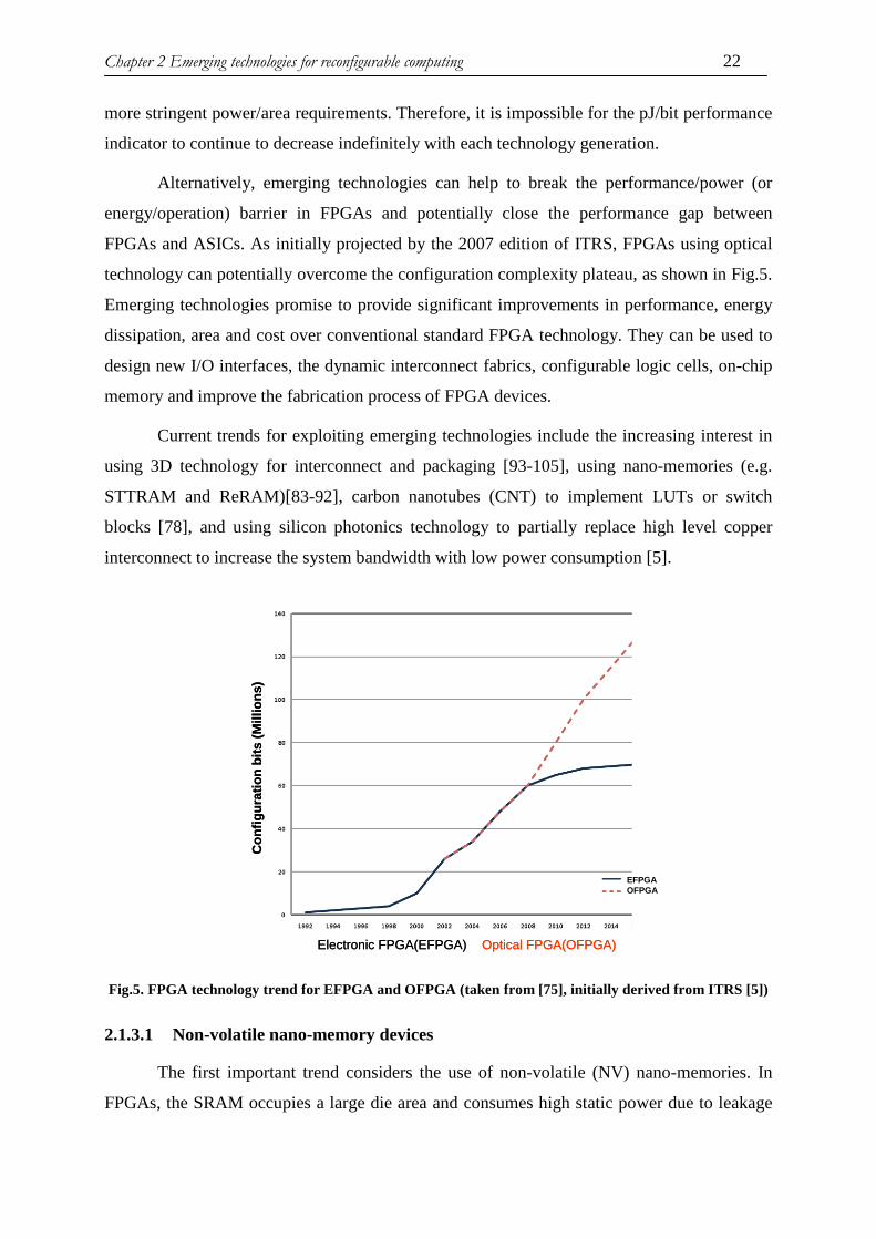
Chapter 2 Emerging technologies for reconfigurable computing 22
more stringent power/area requirements. Therefore, it is impossible for the pJ/bit performance
indicator to continue to decrease indefinitely with each technology generation.
Alternatively, emerging technologies can help to break the performance/power (or
energy/operation) barrier in FPGAs and potentially close the performance gap between
FPGAs and ASICs. As initially projected by the 2007 edition of ITRS, FPGAs using optical
technology can potentially overcome the configuration complexity plateau, as shown in Fig.5.
Emerging technologies promise to provide significant improvements in performance, energy
dissipation, area and cost over conventional standard FPGA technology. They can be used to
design new I/O interfaces, the dynamic interconnect fabrics, configurable logic cells, on-chip
memory and improve the fabrication process of FPGA devices.
Current trends for exploiting emerging technologies include the increasing interest in
using 3D technology for interconnect and packaging [93-105], using nano-memories (e.g.
STTRAM and ReRAM)[83-92], carbon nanotubes (CNT) to implement LUTs or switch
blocks [78], and using silicon photonics technology to partially replace high level copper
interconnect to increase the system bandwidth with low power consumption [5].
EFPGAOFPGA
Con
figur
atio
n bi
ts (M
illio
ns)
Electronic FPGA(EFPGA) Optical FPGA(OFPGA)
EFPGAOFPGA
Con
figur
atio
n bi
ts (M
illio
ns)
Electronic FPGA(EFPGA) Optical FPGA(OFPGA)
Fig.5. FPGA technology trend for EFPGA and OFPGA (taken from [75], initially derived from ITRS [5])
2.1.3.1 Non-volatile nano-memory devices
The first important trend considers the use of non-volatile (NV) nano-memories. In
FPGAs, the SRAM occupies a large die area and consumes high static power due to leakage
Chapter 2 Emerging technologies for reconfigurable computing 23
current. Moreover, the SRAM is volatile, which requires all functions to be reprogrammed at
each power-up. Replacing SRAMs with non-volatile memories to implement logic functions
has been suggested many times in recent years, commonly including using Spin-transfer
torque RAM, ReRAM or Nanocrystal Floating Gate FETs [5]. These emerging memories
offer opportunities to incorporate more programmable logic resources and interconnect in
FPGA chips, as they can create more compact and energy-efficient LUTs or configurable
switch blocks in FPGAs. By leveraging the benefits of these devices, an improvement of
typically 2 to 3 times in the performance/power ratio of FPGAs at the current technology
node is expected to be achieved [95].
Spin-transfer torque RAM (STT-RAM) is considered to be one of the most promising
candidates for non-volatile memory using spintronics technology [76] which combines non-
volatility, excellent scalability and endurance with lower power consumption and high read
and write speeds. Spin-transfer torque data writing is performed by passing an electric current
to change the magnetic orientation of the information storage layer in a magnetic tunnel
junction. By using such writing schemes, STT-RAMs promise to greatly reduce the power
and die area and improve the write selectivity over conventional magnetic memories [77].
Compared with SRAMs, STT-RAMs have a much smaller cell size and an equivalent write
speed. The non-volatile memory based FPGA architecture was proposed by Zhao et al. [77] in
2009 and Torres et al. [79] in 2010. In 2014, FPGAs using STT-RAMs have been
commercialized by Altera and Everspin, with the expectation of improving the application
performance, data security and system crash recovery time according to the designers of
Altera Inc. [80]. The configuration bits can be stored in STT-RAM cells and logic blocks can
then be safely powered off, avoiding significantly noise or power failure. Moreover, the
application of such FPGAs using magnetic memories can be considered to extend to
aerospace or military fields which enable new computing features that conventional FPGAs
cannot offer. For example, Goncalves et al. [83] demonstrated a 2-LUT using a compact
model of the magnetic tunnel junction on hybrid magnetic/CMOS 130nm technology, which
allows an FPGA to be protected against radiation with low area overhead. The main
challenges faced by the STT-RAM technology are i) the stochastic nature of magnetic tunnel
junction, which leads to a non-deterministic transient behavior during switching activity
caused by thermal stability, and ii) the high write energy consumption, given by the high
intrinsic current when switching magnetization[95]. Many schemes have been proposed to
minimize the writing energy while maintaining sufficient thermal stability for acceptable error

Chapter 2 Emerging technologies for reconfigurable computing 24
rates, including relaxing the non-volatility of STT-RAMs through reducing the planar area of
magnetic tunnel junction [85], tuning the saturation magnetization and the thickness of the
free layer, etc. In [85], a cache model is developed to explore the trade-off between the non-
volatility, latency and energy in STT-RAMs, and a more than 70% reduction in energy-delay
product is achieved by using a hybrid design of SRAM-based L1 caches with reduced-
retention STT-RAM L2 and L3 caches. Ping [86] proposed an early write termination scheme
to improve the STT-RAM cache, which reads out the content of the cache before doing a
writing operation, leading to 80% reduction in writing energy and 33% saving in total energy
in their experiments. In addition, some new techniques have been invented to make use of the
stochastic nature of magnetic tunnel junction. Zhang et al. use the stochastic feature as a way
to maintain the thermal stability by proposing a multi-level programmable cell that can
change states randomly.
Another emerging memory technology for FPGA architectures is the rapidly evolving
ReRAM, standing for Redox memory or resistive RAM. ReRAMs are based on a metal-ion
conductor-metal (MIM) structure, which utilizes ion migration with a redox process to
perform the resistive switching operation, involving the dielectric and/or electrode materials.
Since the ReRAM device has the potential to scale down to very small feature sizes, the
switching time can be as low as a few nanoseconds. However, many of the details of the
ReRAM switching mechanisms are still unknown, which is the key challenge for the
development of this technology. Rapid improvement has been made in several kinds of
ReRAM and towards a commercial product, such as:
• the Conductive Bridge RAM that has been demonstrated exhibiting very good scalability
and ultra-low energy dissipation[87],
• the Valence Change Memory which has progressed a lot in scaling (~10nm critical size),
endurance and retention time[89],
• The Thermo-Chemical Memory which can advantageously enable the vertical stacking of
memory devices in a dense crossbar array [92].
In 2013, Toshiba Inc. reported a basic read/write circuit for prototyping a 2-layer 32Gb
ReRAM memory [91] on a 24nm CMOS platform, although details of the switching material
and performance parameters were not given. Using ReRAMs in a reconfigurable switching
application is also very promising [88]. Miyamura et al. proposed a programmable cell array
and a 32x32 crossbar switch using a nonvolatile and rewritable solid-electrolyte switch, with

Chapter 2 Emerging technologies for reconfigurable computing 25
each individual cell functionally equivalent to a 4-LUT. An 81% reduction in cell area and a
72% reduction in total chip-area compared with that of a standard SRAM based design is
achieved on a 90nm CMOS platform.
2.1.3.2 3D technology
The second important trend is Three-dimensional (3D) technology. 3D integration
technology allows for the vertical stacking of layers of basic electronic components that are
laterally connected by using 2D interconnect fabrics. 3D integration includes 3D bonding, 3D
stacking, and the use of a Si interposer structure that only contain interconnect layers. Several
vertical interconnect methods have been explored recently, such as wire bonding,
microbumps, contactless interconnection, and particularly the TSV (Through-Silicon-Via),
which seems to be the most promising of all the candidates [5]. 3D integrated technology is
increasingly viewed as an attractive solution in responding to the critical process-scaling issue
for reducing area and power consumption [87]. As mentioned previously, interconnects have
emerged as the main source of delay and power consumption in microelectronic chips. 3D
integration may offer significant benefits for interconnect such as reduced wire length, higher
memory bandwidth (by stacking the memory and computing cores with TSV connections),
heterogeneous integration and smaller form factor, which can potentially lead to higher
packing density and smaller footprint, and thereby lower fabrication costs [5]. However, 3D
brings new challenges of its own, such as thermal issues, passive and memory interposer
design, clock tree and power grid design as well as other challenges relating to physical and
EDA tools [5,87].
As previously mentioned, the circuit delay in FPGA architectures is determined by the
configurable interconnect part that might need to connect two computing resources at a
significant distance between each other. 3D integration technology can reduce the
interconnect length, thereby providing significant improvement in FPGA performance and
power consumption [93,96,98-100]. Moreover, as the interconnect accounts for a large
portion of the silicon die area, the reduction of the interconnect area results in the reduction of
manufacturing cost for FPGAs. In the past, much work has been done to implement 3D
FPGAs by using 3D routing switches based on electrical or optical technologies [103], or by
partitioning memory elements and routing functions over different layers [100]. Rahman et al.
[101] proposed an analytical model to predict the interconnect bandwidth requirements in
FPGAs, which shows the opportunities for 3D implementation of FPGAs. They use 3D (6-

Chapter 2 Emerging technologies for reconfigurable computing 26
direction) switching blocks for vertical interconnection, and all the FPGA elements were
distributed between layers in a form of fine granularity. Experimental results showed that in a
FPGA containing 70K logic cells that were fabricated in a 0.25µm process, the LUT density
was improved by 25-60% in their proposed 3D implementation. Moreover, the interconnect
delay was also significantly reduced by 45%-60% and the reduction in power dissipation
ranged from 35% to 55%.
[97]proposed a 3D non-volatile FPGA architecture, in which the basic FPGA
structures were renovated, as well as the layer partition and logic density evaluation for 3D
die stacking. By replacing SRAM cells in FPGAs with PCM cells (Fig.6), their simulation
results showed that the logic density per bit can be significantly improved over 16 times
against SRAMs in a basic FPGA architecture. In their work, the 3D integration is realized by
using two layer die stacking: all the interconnect and switch components, as well as the
memory elements in logic blocks are put in one layer; while all the logic blocks are located in
another layer, and in between are the TSVs for corresponding vertical interconnections.
Experimental results showed that the improvement in wire length, interconnect delay and
power consumption was 55%, 45% and 35% respectively in 3D implementation compared
with 2D baseline FPGAs. They also showed better results in logic density, interconnect delay
and power consumption compared to Rahman’s proposal.
Fig.6. The basic FPGA architecture and the PCM cell used in a 3D non-volatile FPGA (source from [97])
In addition, researchers have developed some CAD tools to explore and evaluate the
design using 3D FPGAs. Alexander et al. [98] proposed 3D place and route algorithms.
Ababei et al [104] presented a fast placement tool for 3D FPGAs, in which the effects of 3D
integration on circuit delay taking into account the interconnect wire length are investigated.
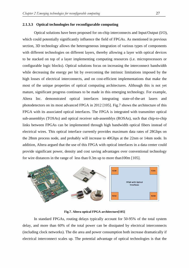
Chapter 2 Emerging technologies for reconfigurable computing 27
2.1.3.3 Optical technologies for reconfigurable computing
Optical solutions have been proposed for on-chip interconnects and Input/Output (I/O),
which could potentially significantly influence the field of FPGAs. As mentioned in previous
section, 3D technology allows the heterogeneous integration of various types of components
with different technologies on different layers, thereby allowing a layer with optical devices
to be stacked on top of a layer implementing computing resources (i.e. microprocessors or
configurable logic blocks). Optical solutions focus on increasing the interconnect bandwidth
while decreasing the energy per bit by overcoming the intrinsic limitations imposed by the
high losses of electrical interconnects, and on cost-efficient implementations that make the
most of the unique properties of optical computing architectures. Although this is not yet
mature, significant progress continues to be made in this emerging technology. For example,
Altera Inc. demonstrated optical interfaces integrating state-of-the-art lasers and
photodetectors on its most advanced FPGA in 2012 [105]. Fig.7 shows the architecture of this
FPGA with its associated optical interfaces. The FPGA is integrated with transmitter optical
sub-assemblys (TOSAs) and optical receiver sub-assemblys (ROSAs), such that chip-to-chip
links between FPGAs can be implemented through high bandwidth optical fibers instead of
electrical wires. This optical interface currently provides maximum data rates of 28Gbps on
the 28nm process node, and probably will increase to 40Gbps at the 22nm or 14nm node. In
addition, Altera argued that the use of this FPGA with optical interfaces in a data center could
provide significant power, density and cost saving advantages over conventional technology
for wire distances in the range of less than 0.3m up to more than100m [105].
Fig.7. Altera optical FPGA architecture[105]
In standard FPGAs, routing delays typically account for 50-95% of the total system
delay, and more than 60% of the total power can be dissipated by electrical interconnects
(including clock networks). The die area and power consumption both increase dramatically if
electrical interconnect scales up. The potential advantage of optical technologies is that the
Chapter 2 Emerging technologies for reconfigurable computing 28
power consumption of an optical link is relatively independent of the line length, and the
optical waveguide loss can be as low as 0.1dB/cm in an SOI platform. In addition, unlike
electrical signals, optical signals are immune to electric-magnetic interference and have less
crosstalk, providing better signal integrity. Moreover, with WDM technology, multiple
independent signals can be transmitted in each optical waveguide, leading to high bandwidth
and lower hardware utilization. [75] predicted in their experiments that if the interconnect
delays could be mitigated through the use of optical technologies, the CelerityTM accelerator
would go from 130MHz to 650MHz with a 500% clock rate improvement. In addition, an
increase of approximately 10 times in configurable logic blocks and computational power
with higher parallelization could be achieved if the interconnect area was decreased by using
silicon photonics and the WDM technology. Indeed, an optical FPGA made with
programmable optical logic cells and optical interconnects was identified as a future direction
for signal processing and optical supercomputing in DARPA/MTO Microsystems technology
symposium in 2007 [56]. The main challenge is to design efficient reconfigurable optical
routers and interconnect architectures that satisfy the flexibility, power, area and cost
requirements. Recent progress has been made by D. Prather et.al [75] who proposed an
optically interconnected reconfigurable switching system based on the confinement and
dispersive properties of photonic crystal structures, which includes fixed planar and 3D
routing structures, crossbar switches for reconfiguration and electro-optic modulators for
signal encoding. Preliminary results show that this system is very promising to replace the full
crossbar switching system.
To take full advantage of optics in future FPGAs architecture, it is crucial that the
programmable optical computation core performs logic operations in the optical domain. If
such an optical logic core could be realized, the optical routing fabric could seamlessly
interconnect all optical logic blocks without electrical-optical conversion interfaces, leading to
a significant reduction of power, area and delay, in a true all-optical FPGA. Within this
context, our work is to propose an optical core implementation of reconfigurable computing
cells by taking full advantage of the silicon photonics technology.
In this section, we briefly overviewed the FPGAs with a focus on emerging
technologies that could offer better performance, energy-efficiency and lower cost for
reconfigurable computing systems. However, to realize their full potential, architectural
innovation is required. For example, emerging non-volatile memory requires re-architecting
memory and storage systems, and optical technologies imply a rethink of the computing

Chapter 2 Emerging technologies for reconfigurable computing 29
architecture to make the most of the properties of light. In the next section, we will discuss
state-of-the-art optical reconfigurable computing architectures.
2.2 State-of-the-art: Silicon photonics based computing architectures
2.2.1 Background
Silicon photonics is an emerging technology platform for implementing photonic
integrated circuits (PIC). On a PIC, information is transferred and processed by using photons
instead of electrons on a chip. There are a range of material candidates for PIC technology:
doped glass, III–V semiconductors, polymers, silicon, and others. Silicon is the most
promising among them due to the high refractive index contrast in the silicon-on-insulator
(SOI) platform. It supports strong confinement of light through defining submicron
waveguide circuits and thus allows the large volume integration of optical functions on a
single chip. As mentioned earlier, the main driving force for silicon photonics is the
development of optical interconnects. But due to its compatibility with CMOS technology
platform, the potential of silicon photonics can be extended to computing as well. Within this
context, new optical computing paradigms inspired by silicon photonics technologies have
been proposed. In this section we first introduce the directed logic circuit and the
reconfigurable directed logic circuit, and finally we discuss their limitations and challenges.
2.2.2 Directed Logic
Directed logic (DL)[111] was introduced as a logic architecture based on modified
optical Fredkin-like gates. A DL architecture is composed of optical switches interconnected
through waveguides. The switching state is controlled by an electrical input logic signal. All
switches can change their state simultaneously with this input electrical signal, and the
operation of each switching element is independent of the operation of the other elements in
the circuit. Fig.8 a) illustrates the basic switching element operations in the DL architecture
for an input vector (1, 0). If the control signal is logic ‘0’, the input vector will pass through
the switch to produce the same result at the output ports as its input (1,0), otherwise, if the
control signal is logic ‘1’, the components of the input vector will be switched at the output,
thus producing a logic vector (0,1).

Chapter 2 Emerging technologies for reconfigurable computing 30
The computation of the logical function is performed by the directed circuit as a whole.
Considering an OR/NOR circuit that is implemented by 3 optical switches [111]: Fig.8 (right
hand side) depicts the circuit with input optical vector (1,0), the input signals A and B control
the operation of each element, and A’ is the replication of A. The output vector of the switch
with control A is split to form intermediate vectors serving as the input of the subsequent
switches (i.e. with control B and A’), which then output the pair of complementary bits of the
required logic operations. For example, if A is logic ‘1’, the scalar 1 takes the bottom path and
then it propagates to the OR output port without being affected by the value of B; otherwise,
if A is logic ‘0’, then the outputs depend on the value of B. Similarly, if B is logic ‘1’, it will
pass the logic ‘1’ to the second downside switch and yields the value ‘1’ at the output port OR,
and the zero value of B will yield the value ‘1’ at the output NOR. The optical signal
representing the value 1 will always arrive at one of the NOR or OR outputs, while the other
will have the value 0. In the same way, other basic logic circuits such as AND/NAND and
XOR/XNOR could be implemented but require a different interconnect.
The main advantage of the DL architecture is the reduction of the latency. Latency is
the sum of the propagation delay on the signal path and the switching delay associated with
the switching state changes. In traditional logic architectures, the switching time for state
change upon the input values are accumulated before the final result is computed. The
operation speed thus decreases with the increasing circuit complexity. However, in this
directed logic circuit, all the switching nodes perform change simultaneously, such that the
circuit is slowed by only a single switch delay on entire path. Another advantage is that the
directed logic can be conservative and reversible, since its number of inputs is equal to its
number of outputs.
The main limitations of this original DL architecture are: first, while DL circuits
improve the computation latency as compared to traditional logic architectures, the
interconnections are fixed and the optical switches are non-configurable, leading to an
application specific architecture. Second, the optical switches are cascaded in such a way that
light has to propagate through a long chain of switches in the worst-case scenario, which
imposes a significant limitation on the scalability of the DL paradigm due to the losses
encountered by the optical signal. Logic minimization and optimization are thus required to
expand the DL paradigm from the implementation of a single logic operation to more
complex computing operations. Moreover, the long optical path will increase the propagation
time of the optical signal. Specifically, when optical micro-resonator based add-drop filters
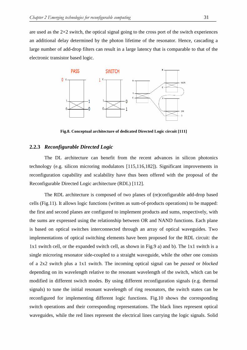
Chapter 2 Emerging technologies for reconfigurable computing 31
are used as the 2×2 switch, the optical signal going to the cross port of the switch experiences
an additional delay determined by the photon lifetime of the resonator. Hence, cascading a
large number of add-drop filters can result in a large latency that is comparable to that of the
electronic transistor based logic.
Fig.8. Conceptual architecture of dedicated Directed Logic circuit [111]
2.2.3 Reconfigurable Directed Logic
The DL architecture can benefit from the recent advances in silicon photonics
technology (e.g. silicon microring modulators [115,116,182]). Significant improvements in
reconfiguration capability and scalability have thus been offered with the proposal of the
Reconfigurable Directed Logic architecture (RDL) [112].
The RDL architecture is composed of two planes of (re)configurable add-drop based
cells (Fig.11). It allows logic functions (written as sum-of-products operations) to be mapped:
the first and second planes are configured to implement products and sums, respectively, with
the sums are expressed using the relationship between OR and NAND functions. Each plane
is based on optical switches interconnected through an array of optical waveguides. Two
implementations of optical switching elements have been proposed for the RDL circuit: the
1x1 switch cell, or the expanded switch cell, as shown in Fig.9 a) and b). The 1x1 switch is a
single microring resonator side-coupled to a straight waveguide, while the other one consists
of a 2x2 switch plus a 1x1 switch. The incoming optical signal can be passed or blocked
depending on its wavelength relative to the resonant wavelength of the switch, which can be
modified in different switch modes. By using different reconfiguration signals (e.g. thermal
signals) to tune the initial resonant wavelength of ring resonators, the switch states can be
reconfigured for implementing different logic functions. Fig.10 shows the corresponding
switch operations and their corresponding representations. The black lines represent optical
waveguides, while the red lines represent the electrical lines carrying the logic signals. Solid

Chapter 2 Emerging technologies for reconfigurable computing 32
squares represent the switches configured to allow an optical signal to pass (or block) when
the logic input is ‘1’ (or ‘0’), while the switches pass (or block) the optical signal when the
logic input is ‘0’ (or ‘1’) are represented by hollow squares. For expanded cells, the square is
replaced by a triangle to represent the case when the optical signal crosses the 2x2 switch and
then it propagates on a waveguide different with the initial one (equivalently represented by
the symbol with two crossing lines in Fig.10).
(c)(a)
(b)
ring (c)(a)
(b)
ring
Fig.9. RDL basic circuit example and switching cell: (a) optical micrograph of a 1x1 electro-optic switch [150] (b) a RDL circuit implemented by 1x1 switches [150] (c) an expanded RDL cell based on a 2x2
switch [111] for realizing XOR port
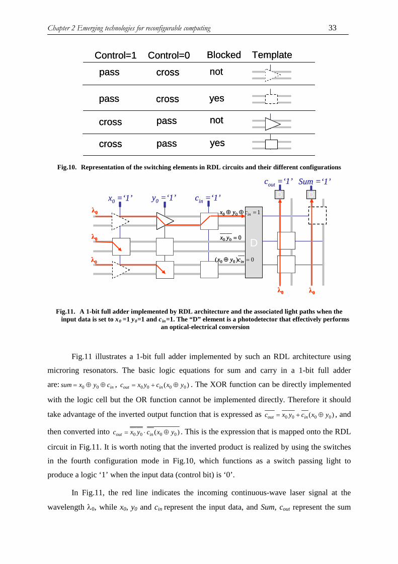
Chapter 2 Emerging technologies for reconfigurable computing 33
Control=1
pass cross
Control=0 Template Blocked
not
cross pass not
pass cross yes
cross pass yes
Control=1
pass cross
Control=0 Template Blocked
not
cross pass not
pass cross yes
cross pass yes
Fig.10. Representation of the switching elements in RDL circuits and their different configurations
D
x0 =‘1’ y0 =‘1’ cin =‘1’λ0
λ0
λ0
cout =‘1’ Sum =‘1’D D
λ0 λ0
100 =⊕⊕ incyx
000 =yx
0)( 00 =⊕ incyx
D
x0 =‘1’ y0 =‘1’ cin =‘1’λ0
λ0
λ0
cout =‘1’ Sum =‘1’D D
λ0 λ0
100 =⊕⊕ incyx
000 =yx
0)( 00 =⊕ incyx
Fig.11. A 1-bit full adder implemented by RDL architecture and the associated light paths when the input data is set to x0 =1 y0=1 and cin=1. The “D” element is a photodetector that effectively performs
an optical-electrical conversion
Fig.11 illustrates a 1-bit full adder implemented by such an RDL architecture using
microring resonators. The basic logic equations for sum and carry in a 1-bit full adder
are: incyxsum ⊕⊕= 00 , )( 0000 yxcyxc inout ⊕+= . The XOR function can be directly implemented
with the logic cell but the OR function cannot be implemented directly. Therefore it should
take advantage of the inverted output function that is expressed as )( 0000 yxcyxc inout ⊕+= , and
then converted into )( 0000 yxcyxc inout ⊕⋅= . This is the expression that is mapped onto the RDL
circuit in Fig.11. It is worth noting that the inverted product is realized by using the switches
in the fourth configuration mode in Fig.10, which functions as a switch passing light to
produce a logic ‘1’ when the input data (control bit) is ‘0’.
In Fig.11, the red line indicates the incoming continuous-wave laser signal at the
wavelength λ0, while x0, y0 and cin represent the input data, and Sum, cout represent the sum

Chapter 2 Emerging technologies for reconfigurable computing 34
and carry-out data at the output. The first plane, based on three pairs of parallel waveguides,
computes three products (one for the Sum and the other two for calculating cout), which are
then converted into electrical signals to control the switches in the second plane through an
OE conversion module (an array of photodetectors, represented by grey squares in Fig.11). In
the example of Fig.11 (when x0 =1 y0=1 and cin=1), the optical signal injected on the highest
horizontal waveguide propagates through the first switch, crosses successively the second one
and the third one before reaching the OE conversion module, thereby generating an electrical
signal of logic ‘1’ for tuning the switch on the second output column to the “pass” state. As a
result, light injected from the bottom of the vertical waveguide in the second plane can reach
the photodetector, thus producing a logic ‘1’ at the output port Sum. For computing the cout,
since the input optical signals are blocked by the second switch in the first plane, the control
bits for the switches on the first vertical waveguide are logic ‘0’. Upon the configuration of
these switches, light directly passes them and generates a logic ‘1’ on the output port cout. In
the worst-case scenario, light has to pass two crossing-state switches and one pass-state
switch in the product plane, 1 photodetector between the two planes, 3 off-resonant switches
in the sum plane and 1 photodetector at the output port.
The RDL architecture has significant limitations. In RDL, logic functions must be
expressed in the form of sums of products, which are typically fed into the integrated photonic
circuit via a two-plane cascaded full cross-bar network of electrically controlled
microresonators, leading to significant hardware cost for this programmable architecture. For
example, to implement a k-bit full adder (the number of input bit is 2k+1, the number of
output bit is k+1) with RDL architecture using expanded cells (each requiring three
microrings), k2+k+1 products are required, and 3(k2+k+1)(3k+2) microring resonators, as well
as k2+2k+2 lasers and photodetectors are needed.
Indeed, considering the history related to the design of reconfigurable computing
architectures, the area costs of two-plane implementations quickly become prohibitive. In
addition, RDL circuits do not allow multiple and distinct operations to be computed
simultaneously using different wavelengths1. Yet, the parallelism as offered by WDM to save
energy and hardware resources is a major advantage of optics for computing. As we will
present in Chapter 3 , to make the most of silicon photonic technologies, the use of WDM is a
fundamental vector for creating powerful computing architectures. 1 In RDL multi-spectral circuit, multiple wavelengths are used to perform a single operation and generate one output bit[150]

Chapter 2 Emerging technologies for reconfigurable computing 35
2.3 Conclusions
In this chapter, we presented an overview of FPGA architectures and discuss the current
trends of emerging technologies for implementing reconfigurable computing architectures
that could offer better performance, energy efficiency and cost. We then examined the state-
of-the-art optical computing architectures, and showed that the optical approaches can be used
to implement reconfigurable computing systems with the promise of reduced latency and
energy dissipation.

Chapter 2 Emerging technologies for reconfigurable computing 36

Chapter 3 OLUT Architecture Design and Implementation 37
Chapter 3 OLUT ARCHITECTURE DESIGN AND IMPLEMENTATION
In this chapter, we propose a novel reconfigurable logic architecture, the so-called
OLUT architecture, specifically designed to exploit integrated silicon photonics for on-chip
reconfigurable computing. The logical architecture introduced here enables the parallel
implementation of combinational Boolean functions on input data through the use of WDM,
making the most of silicon photonics technology. Section 3.1 first presents the principle of the
OLUT architecture through a basic OLUT block with single output, which performs logic
operations as an electronic LUT. We generalize the basic OLUT block to produce multiple
output bits for performing parallel computations simultaneously (Section 3.2), by taking
advantage of a unique feature of optics, i.e. WDM. We then qualitatively evaluate the
performance of this architecture through the example of 1-bit full adder. In section 3.3, we
further increase the parallelism level of OLUT architecture by exploring the complementary
logic interface, which enables better computation performance and lower energy-per-bit over
the initial OLUT architecture with reasonable area and hardware overhead.
3.1 Single-output OLUT Architecture
3.1.1 From electrical LUTs to optical LUTs
OLUTs are directly inspired from electrical LUTs [108]. As presented in Section 2.1,
an n-input LUT is interfaced through n data inputs, one data output and 2n configuration
inputs connected to 2n bits static RAM (SRAM) memory. Computation is achieved by directly
indexing, from input data, the operation result stored in the memory. Fig.12(a) shows an
electrical 2-LUT circuit layout. It is built out of 4 memory bits and a 4:1 multiplexer. In
electrical FPGAs, the main advantages of LUTs are the constant computation time and their
ability to realize any Boolean function depending on the state of the SRAM, leading to highly
flexible architectures [54, 55].
A 2-OLUT block, providing a behavior equivalent to that of an electrical 2-LUT, is
presented in Fig.13 (b). It uses an input optical signal at a wavelength λ0 as the equivalent of a

Chapter 3 OLUT Architecture Design and Implementation 38
power supply. The OLUT block has its input and output data in electrical form. Similarly to
the electrical LUT, the OLUT is composed of two parts [108]:
Routing part (left half of Fig.12 (b)): According to the electrical data inputs, a set of
interconnected optical routers (for a possible implementation, see section 4.1.1) drive the
optical signal into one of the horizontal waveguides, acting as a 1:4 demultiplexer network.
Memorization part (right half of Fig.12 (b)): composed of four electrically controlled
add-drop filters and interconnected by four horizontal waveguides, it produces the required
Boolean computation on the incoming electrical data. As for electrical LUTs, the executed
Boolean function depends on the configuration bits stored in the SRAM memories that
control the optical switches: logic '1' and '0' will respectively turn the attached add-drop filter
to on- or off-resonance, thereby generating the corresponding output logic at the photodetector
(brightness: logic ‘1’ and darkness: logic ‘0’).
0/1
y z0
λ0
λ0
λ0
λ0
D
SRAM Multiplexer
λ00/1
xy
Z0
xInput Data Input Data Output Data
Output Data
(b) Optical 2-LUT
SRAM
(a) Electrical 2-LUT
λ0 stage
0/1
0/1
0/1
Routing Memorization
λ00/1
λ00/1
λ00/1
0/10/1
y z0
λ0
λ0
λ0
λ0
D
SRAM Multiplexer
λ00/1 λ00/1
xy
Z0
xInput Data Input Data Output Data
Output Data
(b) Optical 2-LUT
SRAM
(a) Electrical 2-LUT
λ0 stage
0/10/1
0/10/1
0/10/1
Routing Memorization
λ00/1 λ00/1
λ00/1 λ00/1
λ00/1 λ00/1
Fig.12. Schematic representation of (a) an electrical 2-LUT and (b) its equivalent OLUT.
3.1.2 Basic principle and switching operation
The switching element actually holds the key functionality of selecting and redirecting
an optical signal based on its wavelength. For clarity, we use different symbols for the optical
routers and the optical switches in Fig.12, in the routing and the memorization part
respectively, although these could all be physically implemented with the same optical
component, for instance a microring resonator based add-drop filter (as explained in chapter
4). The relevance of this distinction will become more explicit when introducing the use of
WDM in OLUT architectures in order to parallelize computations.
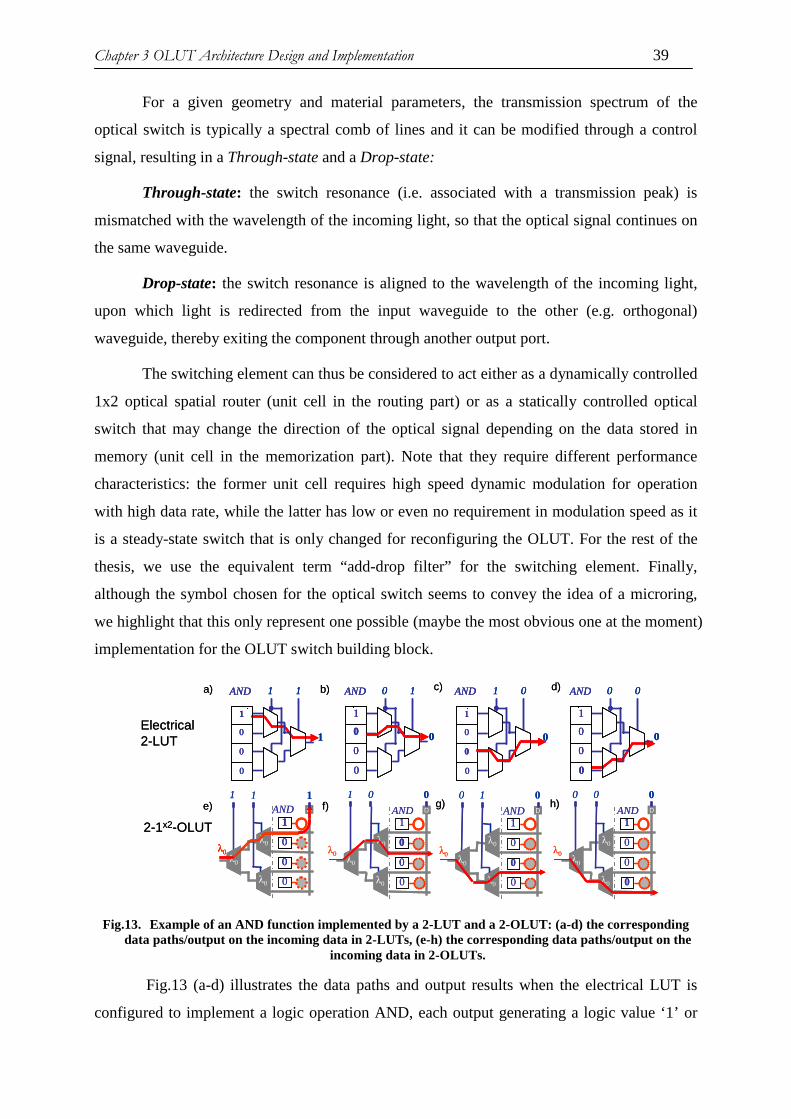
Chapter 3 OLUT Architecture Design and Implementation 39
For a given geometry and material parameters, the transmission spectrum of the
optical switch is typically a spectral comb of lines and it can be modified through a control
signal, resulting in a Through-state and a Drop-state:
Through-state: the switch resonance (i.e. associated with a transmission peak) is
mismatched with the wavelength of the incoming light, so that the optical signal continues on
the same waveguide.
Drop-state: the switch resonance is aligned to the wavelength of the incoming light,
upon which light is redirected from the input waveguide to the other (e.g. orthogonal)
waveguide, thereby exiting the component through another output port.
The switching element can thus be considered to act either as a dynamically controlled
1x2 optical spatial router (unit cell in the routing part) or as a statically controlled optical
switch that may change the direction of the optical signal depending on the data stored in
memory (unit cell in the memorization part). Note that they require different performance
characteristics: the former unit cell requires high speed dynamic modulation for operation
with high data rate, while the latter has low or even no requirement in modulation speed as it
is a steady-state switch that is only changed for reconfiguring the OLUT. For the rest of the
thesis, we use the equivalent term “add-drop filter” for the switching element. Finally,
although the symbol chosen for the optical switch seems to convey the idea of a microring,
we highlight that this only represent one possible (maybe the most obvious one at the moment)
implementation for the OLUT switch building block.
1
0
0
0
0 1
0
AND
1
0
0
0
1 1
1
AND
D
1
λ0
λ0
λ0 0
0
0
λ0
1 1 1AND D
1
λ0
λ0
λ0 0
0
0
λ0
1 0 0AND
1
0
0
0
0 0
0
AND
D
1
λ0
λ0
λ0 0
0
0
λ0
0 0 0AND
1
0
0
0
1 0
0
AND
Electrical 2-LUT
2-1x2-OLUT
a) b) c) d)
e) f) g) h)D
1
λ0
λ0
λ0 0
0
0
λ0
0 1 0AND
1
0
0
0
0 1
0
AND
1
0
0
0
0 1
0
AND
1
0
0
0
1 1
1
AND
1
0
0
0
1 1
1
AND
D
11
λ0
λ0
λ0 00
00
0
λ0λ0λ0
1 1 1AND D
1
λ0
λ0
λ0 00
00
0
λ0
1 0 0AND
1
0
0
0
0 0
0
AND
1
0
0
0
0 0
0
AND
D
11
λ0
λ0
λ0 0
0
0
λ0
0 0 0AND
1
0
0
0
1 0
0
AND
1
0
0
0
1 0
0
AND
Electrical 2-LUT
2-1x2-OLUT
a) b) c) d)
e) f) g) h)D
11
λ0
λ0
λ0 0
0
0
λ0
0 1 0AND
Fig.13. Example of an AND function implemented by a 2-LUT and a 2-OLUT: (a-d) the corresponding
data paths/output on the incoming data in 2-LUTs, (e-h) the corresponding data paths/output on the incoming data in 2-OLUTs.
Fig.13 (a-d) illustrates the data paths and output results when the electrical LUT is
configured to implement a logic operation AND, each output generating a logic value ‘1’ or

Chapter 3 OLUT Architecture Design and Implementation 40
‘0’ according to the electrical voltage. Fig.13 (e-h) show the corresponding scenarios in a 2-
OLUT configured to process the equivalent logic function using a light beam at λ0. In OLUTs,
the corresponding output logic is generated according to the presence of light (scenario (e):
logic ‘1’) or its absence (scenario (f)-(h): logic ‘0’) at the photodetector. For clarity, we
represent the on(/off)-resonance switches that are spectrally (mis)matched with the incoming
light signal by solid (/dotted) lines.
3.2 n-m-OLUT architecture
3.2.1 Operation principles
As mentioned previously, to make the most of silicon photonic technologies, the use
of WDM is a fundamental vector for creating powerful computing architectures. While the
OLUT described in Fig.12 (b) uses a single optical signal at wavelength λ0 thereby computing
a single operation as in traditional LUTs, WDM can be advantageously implemented in
OLUTs to realize simultaneous logic operations on the same input data. In this way, OLUTs
potentially allow us to increase the performance/power ratio as compared to electrical LUTs.
An m operation OLUT (so-called n-m-OLUT) thus interfaces n electrical data inputs
to m electrical data outputs, using m optical signals at distinct wavelengths (λ0,..., λm-1). In the
routing part, the m optical signals λi ( i = 0…m-1) share the same optical path specified by the
electrical input data set. In the memorization part, they are driven into m memorization stages
(represented by m distinct columns), each of which is composed of 2n identical add-drop
filters and interconnected by 2n horizontal waveguides. Each stage of the memorization part
performs a basic Boolean function through a specific wavelength, all the stages operating in
parallel thanks to WDM.
Fig.14 depicts the example of a 2-4-OLUT configured to simultaneously process logic
operations AND, OR, XOR, and XNOR at four different wavelengths, namely λ0, λ1, λ2 and λ3
respectively. All four optical signals are driven, through the routing part, into one of the four
horizontal waveguides of the memorization part according to the values of x and y input data.
In the example of Fig.14 , the input values x= ‘1’ and y= ‘1’, drive the optical signals towards
the first waveguide at the top. The optical signals will then propagate across the memorization
part and, depending on the state of the crossed switches (as controlled by the SRAM
configuration), each wavelength will continue on the same horizontal waveguide or will be

Chapter 3 OLUT Architecture Design and Implementation 41
selectively dropped to the vertical one, thereby producing a logic ‘0’ or a logic ‘1’ at the
associated outputs. In this example, the optical signals at wavelength λ0, λ1 and λ3 are
redirected into the vertical waveguides, resulting in ‘1’ logic values on the Z0, Z1 and Z3
output ports, while the optical signal at λ2 continues along the horizontal waveguide, resulting
in logic ‘0’ at the output Z2.
YX
1
Routing part Memorization part
1
1 1
1
1
0
0 1
0
0
0
1
0
λx
λx
D D D D
λ0
λ0
λ0
λ0
λ1
λ1
λ1
λ1 λ2
λ2
λ2
λ2
λ3
0 λ3
λ3
0 λ3
AND OR XOR Buffer
λ0λ1λ2λ3
Z0 Z1 Z2 Z3‘1’ ‘1’ ‘1’ ‘1’ ‘1’‘0’
λx
YX
1
Routing part Memorization part
1
1 1
1
1
0
0 1
0
0
0
1
0
λx
λx
D D D D
λ0
λ0
λ0
λ0
λ1
λ1
λ1
λ1 λ2
λ2
λ2
λ2
λ3
0 λ30 λ3
λ3
0 λ30 λ3
AND OR XOR Buffer
λ0λ1λ2λ3
Z0 Z1 Z2 Z3‘1’ ‘1’ ‘1’ ‘1’ ‘1’‘0’
λx
Fig.14. Functional representation of a 2-4-OLUT configured for processing parallel logic operations at
four wavelengths.
In the OLUT architecture, WDM is implemented by using two different wavelength
filtering schemes (i) in the routing part, where all the optical signals, independently of their
wavelength, are propagated along the same path, and (ii) in the memorization part, where each
spectrally distinct optical signal is individually routed according to the configuration. For the
2-4-OLUT example (Fig.14):
Routing part: The behavior of the switch in the routing part is illustrated in the Fig.15
(a) according to its DROP state (solid line) or THROUGH state (dashed line). The arrows
represent the four incident optical signals for which the wavelength values λ0, λ1, λ2 and λ3 are
either ideally aligned with the switch resonant wavelengths (represented by peaks in the
transmission spectrum) in the DROP state, or detuned by a wavelength difference ∆λ in the
THROUGH state. The wavelengths of the injected optical signal are regularly spaced
consistently with the Free Spectral Range (FSRx) of the switch. Hence, in case the add-drop
filter is in the DROP state, all the signals are redirected to a given waveguide while, in the
THROUGH state, all the signals propagate along the other waveguide.

Chapter 3 OLUT Architecture Design and Implementation 42
Memorization part: Fig.15 (b) and (c) illustrate the operation of the add-drop filters
in the memorization part as well as their transmission spectrum. Compared to those of the
routing part, their FSR is slightly larger (see FSRm0 and FSRm1 in Fig.15 (b) and (c)) so that
at most one resonant wavelength is aligned with one wavelength of the injected optical signal:
λ0 in (b) and λ1 in (c), respectively. In addition, their relative FSR should be slightly different
to avoid the potential scenario where the add-drop resonances become aligned with the
wavelength of the other optical signals after the tuning/detuning process. Having different
FSR and distinct resonant wavelengths in the memorization part can be achieved by changing
the device geometry (e.g. the microring radius) or through a thermal control [119]. As a result,
only one signal wavelength is redirected to the vertical waveguide when the add-drop is
switched to the DROP state (solid line), the other ones propagating through the same
waveguide. Similarly to the add drop used in the routing part, all the signals propagate along
the horizontal waveguide if the add-drop filter is in the THROUGH state (dashed line).
While the 2-4-OLUT example is used to illustrate how basic logic operations are
processed in OLUTs when using the WDM scheme, it should be reiterated that the dimension
of OLUTs can be extrapolated to perform complex Boolean logic function on a larger number
of inputs. By exploiting this feature, OLUTs can realize more specific applications such as
full adders or Arithmetic Logic Units (ALU).

Chapter 3 OLUT Architecture Design and Implementation 43
1λ0λ1λ2λ3λx
0
λx λ0λ2λ3
λ1
FSRx
λλ0 λ1 λ2 λ3
ON Resonance OFF Resonance
1
0
λ0
λ1λ2λ3
λ01
λ0λ1λ2λ3
λ00
FSRm0
λλ0 λ1 λ2 λ3
1
0
λ1
λ0λ2λ3
λ11
λ0λ1λ2λ3
λ10
FSRm1
λλ0 λ1 λ2 λ3
1
0
THROUGH
a) Router
b) λ0
λ1
Transmission Spectrum at Drop port
DROP
DROP
DROP
THROUGH
DROP
THROUGH
DROP
THROUGH
DROP
THROUGH
THROUGH
Memorization Stage
c)Memorization Stage
1λ0λ1λ2λ3
λ0λ1λ2λ3λx
0
λx λ0λ2λ3
λ1
FSRx
λλ0 λ1 λ2 λ3
ON Resonance OFF Resonance
1
0
λ0
λ1λ2λ3
λ01
λ0λ1λ2λ3
λ00
FSRm0
λλ0 λ1 λ2 λ3
1
0
λ1
λ0λ2λ3
λ11
λ0λ1λ2λ3
λ10
FSRm1
λλ0 λ1 λ2 λ3
1
0
THROUGH
a) Router
b) λ0
λ1
Transmission Spectrum at Drop port
DROP
DROP
DROP
THROUGH
DROP
THROUGH
DROP
THROUGH
DROP
THROUGH
THROUGH
Memorization Stage
c)Memorization Stage
Fig.15. Illustration of wavelength filtering schemes in the 2-4-OLUT. In a) router: when the add-drop
filter is in the DROP state, all the signals are redirected to the DROP port and when in the THROUGH state, all optical signals propagate along the other waveguide. The transmission at the DROP port is represented on the right column. In b) λ0 and c) λ1 memorization stage, only one signal wavelength (i.e. λ0 and λ1) is redirected to the vertical waveguide when the add-drop is switched to the DROP state, the other ones propagating through the same waveguide, and all the signals will be forward to the THOUGH port if the add drop is in the THROUGH state
3.2.2 Preliminary evaluation of n-m-OLUTs
The motivation of this early comparison is to i) evaluate the scalability and ii)
qualitatively estimate the potential of OLUT architectures as compared with RDL
architectures [112]. Therefore, here we introduce a few key metrics to evaluate the hardware
efficiencies (i.e. area size and power consumption) and the performance of n-m-OLUTs when
increasing the number of input and output bits. Hence, the scalability of the OLUT
architecture using WDM is estimated and the performance of OLUTs is compared with RDL
for the full adder case. An in-depth study of OLUT performance and power consumption,
taking into account the system constraints, will be carried out through the design space
exploration in Chapter 5.
3.2.2.1 Evaluation Metrics
The area and power consumption relies on hardware resources used in OLUTs. The
area is an estimation of the surface occupied by the add-drop filters. Here, we estimate the
system area size by qualitatively counting the total number of add-drop filters (NAD) in the n-

Chapter 3 OLUT Architecture Design and Implementation 44
m-OLUT, as the sum of the number of add-drops in the routing part (NR) and in the
memorization part (NS) (see Fig.16):
nnSRAD mNNN 212 ×+−=+= (3.1)
In n-m-OLUTs, the electrical power consumption depends on the number of active
devices, i.e. the number of lasers (m), photodetectors (m) and add-drop filters (NAD). Note that
for increasing n and m values, the add-drop filters rapidly pre-dominate the whole n-m-OLUT
architecture, and become the critical building block. The detailed calculation of the energy
consumption will be presented in the section 4.3 of the next chapter along with the device
physical parameters, since these matters strongly depend on the specific implementation
chosen for building the OLUT. In the following full adder case though, we analyze the
scalability through counting the number of active devices for drawing an early comparison
with RDL architectures.
The last metric is the latency. The main contributions to the latency consist of the
conversion time at the O/E interface (the time delay introduced by photodetector, τconv), the
switching time for the routing part (τsw) and the accumulated time to cross each add-drop in
the resonant state (for example τres~10ps for a microring-based add-drop filter with Q~10000),
both in the routing and the memorization parts. This time is much larger than the one needed
to cross the add-drop in the THROUGH state. In addition, note that τsw is equal to the
switching time of a single router unit cell (i.e. ~1ns for the example of electrically controlled
silicon microrings [116,115,112,150]) since all the router cell states are changed by the data
in parallel. By considering the worst-case scenario, where light passes through n resonant
routers in the routing part and one resonant switch in the memorization part, we estimate the
associated total n-m-OLUT latency to be
resswconvolut n tttt ×+++= )1( (3.2)
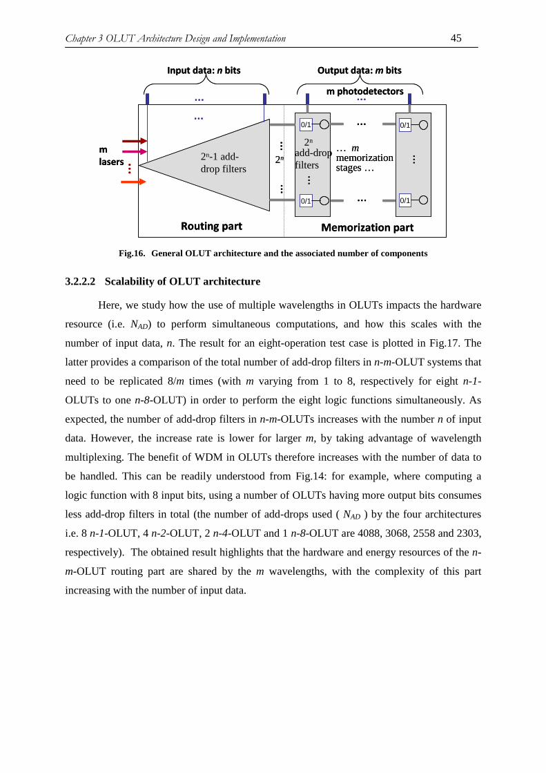
Chapter 3 OLUT Architecture Design and Implementation 45
2n
Routing part Memorization part
…
……
…0/1
… …
m lasers
… mmemorization stages …
…
…
… …
0/1
0/1
0/1
2n-1 add-drop filters
add-drop filters
m photodetectors
2n
Input data: n bits Output data: m bits
2n
Routing part Memorization part
…
……
…0/10/1
… …
m lasers
… mmemorization stages …
…
…
… …
0/10/1
0/10/1
0/10/1
2n-1 add-drop filters
add-drop filters
m photodetectors
2n
Input data: n bits Output data: m bits
Fig.16. General OLUT architecture and the associated number of components
3.2.2.2 Scalability of OLUT architecture
Here, we study how the use of multiple wavelengths in OLUTs impacts the hardware
resource (i.e. NAD) to perform simultaneous computations, and how this scales with the
number of input data, n. The result for an eight-operation test case is plotted in Fig.17. The
latter provides a comparison of the total number of add-drop filters in n-m-OLUT systems that
need to be replicated 8/m times (with m varying from 1 to 8, respectively for eight n-1-
OLUTs to one n-8-OLUT) in order to perform the eight logic functions simultaneously. As
expected, the number of add-drop filters in n-m-OLUTs increases with the number n of input
data. However, the increase rate is lower for larger m, by taking advantage of wavelength
multiplexing. The benefit of WDM in OLUTs therefore increases with the number of data to
be handled. This can be readily understood from Fig.14: for example, where computing a
logic function with 8 input bits, using a number of OLUTs having more output bits consumes
less add-drop filters in total (the number of add-drops used ( NAD ) by the four architectures
i.e. 8 n-1-OLUT, 4 n-2-OLUT, 2 n-4-OLUT and 1 n-8-OLUT are 4088, 3068, 2558 and 2303,
respectively). The obtained result highlights that the hardware and energy resources of the n-
m-OLUT routing part are shared by the m wavelengths, with the complexity of this part
increasing with the number of input data.
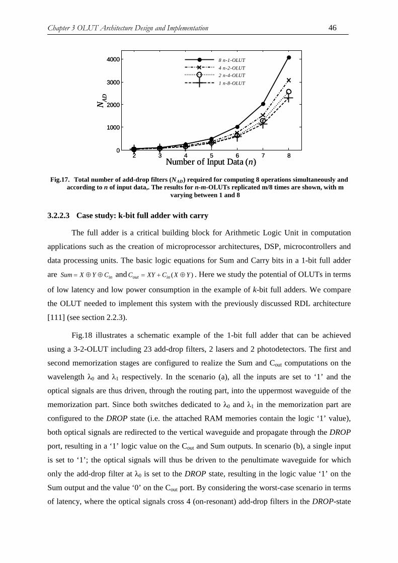
Chapter 3 OLUT Architecture Design and Implementation 46
Number of Input Data (n)
N AD
2 3 4 5 6 7 80
1000
2000
3000
4000
8 n-1-OLUT 4 n-2-OLUT 2 n-4-OLUT 1 n-8-OLUT
Number of Input Data (n)
N AD
2 3 4 5 6 7 80
1000
2000
3000
4000
8 n-1-OLUT 4 n-2-OLUT 2 n-4-OLUT 1 n-8-OLUT
Fig.17. Total number of add-drop filters (NAD) required for computing 8 operations simultaneously and
according to n of input data,. The results for n-m-OLUTs replicated m/8 times are shown, with m varying between 1 and 8
3.2.2.3 Case study: k-bit full adder with carry
The full adder is a critical building block for Arithmetic Logic Unit in computation
applications such as the creation of microprocessor architectures, DSP, microcontrollers and
data processing units. The basic logic equations for Sum and Carry bits in a 1-bit full adder
are inCYXSum ⊕⊕= and )( YXCXYC inout ⊕+= . Here we study the potential of OLUTs in terms
of low latency and low power consumption in the example of k-bit full adders. We compare
the OLUT needed to implement this system with the previously discussed RDL architecture
[111] (see section 2.2.3).
Fig.18 illustrates a schematic example of the 1-bit full adder that can be achieved
using a 3-2-OLUT including 23 add-drop filters, 2 lasers and 2 photodetectors. The first and
second memorization stages are configured to realize the Sum and Cout computations on the
wavelength λ0 and λ1 respectively. In the scenario (a), all the inputs are set to ‘1’ and the
optical signals are thus driven, through the routing part, into the uppermost waveguide of the
memorization part. Since both switches dedicated to λ0 and λ1 in the memorization part are
configured to the DROP state (i.e. the attached RAM memories contain the logic ‘1’ value),
both optical signals are redirected to the vertical waveguide and propagate through the DROP
port, resulting in a ‘1’ logic value on the Cout and Sum outputs. In scenario (b), a single input
is set to ‘1’; the optical signals will thus be driven to the penultimate waveguide for which
only the add-drop filter at λ0 is set to the DROP state, resulting in the logic value ‘1’ on the
Sum output and the value ‘0’ on the Cout port. By considering the worst-case scenario in terms
of latency, where the optical signals cross 4 (on-resonant) add-drop filters in the DROP-state
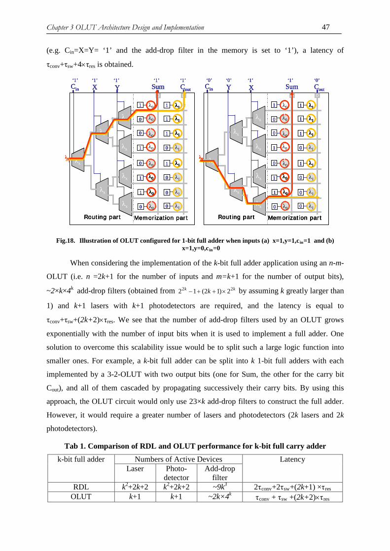
Chapter 3 OLUT Architecture Design and Implementation 47
(e.g. Cin=X=Y= ‘1’ and the add-drop filter in the memory is set to ‘1’), a latency of
τconv+τsw+4×τres is obtained.
1
Routing part Memorization part
1
1
1
0
0
0
1λx
λx
λx
CoutD D
λ0
λ0
λ0
λ0
λ1
λ1
λ1
λ1
λx
λx
λx
0
0
1
0
1
0
1
0
λ0
λ0
λ0
λ0
λ1
λ1
λ1
λ1λx
SumCin X Y‘1’ ‘1’ ‘1’ ‘1’ ‘1’
λ1λ0
1
Routing part Memorization part
1
1
1
0
0
0
1λx
λx
λx
CoutD D
λ0
λ0
λ0
λ0
λ1
λ1
λ1
λ1
λx
λx
λx
0
0
1
0
1
0
1
0
λ0
λ0
λ0
λ0
λ1
λ1
λ1
λ1λx
SumCin X Y‘1’ ‘1’ ‘1’ ‘1’ ‘1’
1
Routing part Memorization part
1
1
1
0
0
0
1λx
λx
λx
CoutD D
λ0
λ0
λ0
λ0
λ1
λ1
λ1
λ1
λx
λx
λx
0
0
1
0
1
0
1
0
λ0
λ0
λ0
λ0
λ1
λ1
λ1
λ1λx
SumCin X Y
1
Routing part Memorization part
1
1
1
0
0
0
1λx
λx
λx
CoutD D
λ0
λ0
λ0
λ0
λ1
λ1
λ1
λ1
λx
λx
λx
0
0
1
0
1
0
1
0
λ0
λ0
λ0
λ0
λ1
λ1
λ1
λ1λx
SumCin X Y‘1’ ‘1’ ‘1’ ‘1’ ‘1’
λ1λ0
1
Routing part Memorization part
1
1
1
0
0
0
1λx
λx
λx
CoutD D
λ0
λ0
λ0
λ0
λ1
λ1
λ1
λ1
λx
λx
λx
0
0
1
0
1
0
1
0
λ0
λ0
λ0
λ0
λ1
λ1
λ1
λ1λx
SumCin Y X‘0’ ‘0’ ‘1’ ‘1’ ‘0’
λ1λ0
1
Routing part Memorization part
1
1
1
0
0
0
1λx
λx
λx
CoutD D
λ0
λ0
λ0
λ0
λ1
λ1
λ1
λ1
λx
λx
λx
0
0
1
0
1
0
1
0
λ0
λ0
λ0
λ0
λ1
λ1
λ1
λ1λx
SumCin Y X‘0’ ‘0’ ‘1’ ‘1’ ‘0’
λ1λ0
1
Routing part Memorization part
1
1
1
0
0
0
1λx
λx
λx
CoutD D
λ0
λ0
λ0
λ0
λ1
λ1
λ1
λ1
λx
λx
λx
0
0
1
0
1
0
1
0
λ0
λ0
λ0
λ0
λ1
λ1
λ1
λ1λx
SumCin Y X
1
Routing part Memorization part
1
1
1
0
0
0
1λx
λx
λx
CoutD D
λ0
λ0
λ0
λ0
λ1
λ1
λ1
λ1
λx
λx
λx
0
0
1
0
1
0
1
0
λ0
λ0
λ0
λ0
λ1
λ1
λ1
λ1λx
SumCin Y X‘0’ ‘0’ ‘1’ ‘1’ ‘0’
λ1λ0
Fig.18. Illustration of OLUT configured for 1-bit full adder when inputs (a) x=1,y=1,cin=1 and (b) x=1,y=0,cin=0
When considering the implementation of the k-bit full adder application using an n-m-
OLUT (i.e. n =2k+1 for the number of inputs and m=k+1 for the number of output bits),
~2×k×4k add-drop filters (obtained from kk k 22 2)12(12 ×++− by assuming k greatly larger than
1) and k+1 lasers with k+1 photodetectors are required, and the latency is equal to
τconv+τsw+(2k+2)×τres. We see that the number of add-drop filters used by an OLUT grows
exponentially with the number of input bits when it is used to implement a full adder. One
solution to overcome this scalability issue would be to split such a large logic function into
smaller ones. For example, a k-bit full adder can be split into k 1-bit full adders with each
implemented by a 3-2-OLUT with two output bits (one for Sum, the other for the carry bit
Cout), and all of them cascaded by propagating successively their carry bits. By using this
approach, the OLUT circuit would only use 23×k add-drop filters to construct the full adder.
However, it would require a greater number of lasers and photodetectors (2k lasers and 2k
photodetectors).
Tab 1. Comparison of RDL and OLUT performance for k-bit full carry adder
k-bit full adder Numbers of Active Devices Latency Laser Photo-
detector Add-drop
filter RDL k2+2k+2 k2+2k+2 ~9k3 2τconv+2τsw+(2k+1) ×τres
OLUT k+1 k+1 ~2k×4k τconv + τsw +(2k+2)×τres
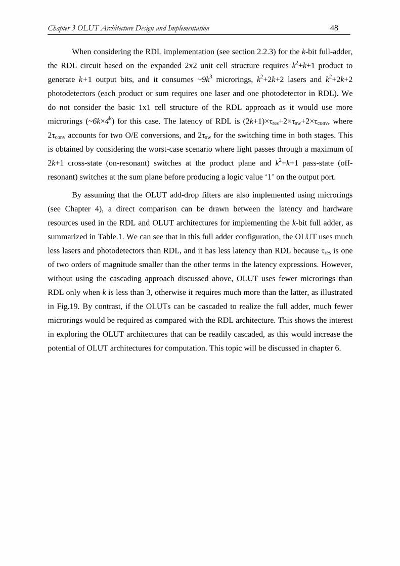
Chapter 3 OLUT Architecture Design and Implementation 48
When considering the RDL implementation (see section 2.2.3) for the k-bit full-adder,
the RDL circuit based on the expanded 2x2 unit cell structure requires k2+k+1 product to
generate k+1 output bits, and it consumes ~9k3 microrings, k2+2k+2 lasers and k2+2k+2
photodetectors (each product or sum requires one laser and one photodetector in RDL). We
do not consider the basic 1x1 cell structure of the RDL approach as it would use more
microrings (~6k×4k) for this case. The latency of RDL is (2k+1)×τres+2×τsw+2×τconv, where
2τconv accounts for two O/E conversions, and 2τsw for the switching time in both stages. This
is obtained by considering the worst-case scenario where light passes through a maximum of
2k+1 cross-state (on-resonant) switches at the product plane and k2+k+1 pass-state (off-
resonant) switches at the sum plane before producing a logic value ‘1’ on the output port.
By assuming that the OLUT add-drop filters are also implemented using microrings
(see Chapter 4), a direct comparison can be drawn between the latency and hardware
resources used in the RDL and OLUT architectures for implementing the k-bit full adder, as
summarized in Table.1. We can see that in this full adder configuration, the OLUT uses much
less lasers and photodetectors than RDL, and it has less latency than RDL because τres is one
of two orders of magnitude smaller than the other terms in the latency expressions. However,
without using the cascading approach discussed above, OLUT uses fewer microrings than
RDL only when k is less than 3, otherwise it requires much more than the latter, as illustrated
in Fig.19. By contrast, if the OLUTs can be cascaded to realize the full adder, much fewer
microrings would be required as compared with the RDL architecture. This shows the interest
in exploring the OLUT architectures that can be readily cascaded, as this would increase the
potential of OLUT architectures for computation. This topic will be discussed in chapter 6.

Chapter 3 OLUT Architecture Design and Implementation 49
1 2 3 4 5 6 7 810
1
102
103
104
105
106
107
k
Num
ber o
f mic
rorin
gs OLUTRDL
)23)(12(3: 2 +++ kkkRDL
)1(212: 1212 +×+− ++ kOLUT kk
1 2 3 4 5 6 7 810
1
102
103
104
105
106
107
k
Num
ber o
f mic
rorin
gs OLUTRDL
1 2 3 4 5 6 7 810
1
102
103
104
105
106
107
k
Num
ber o
f mic
rorin
gs OLUTRDL
)23)(12(3: 2 +++ kkkRDL
)1(212: 1212 +×+− ++ kOLUT kk
Fig.19. Total number of microrings required for implementing a k-bit full adder with the OLUT architecture (represented by red lines with square) and the RDL architecture (represented by blue
lines with triangle)
Therefore, we may conclude that OLUTs allow for lower latency and a reduced
number of lasers and photodetectors, hence reducing the energy consumption in this full adder
configuration when compared to RDL circuits. It also indicates the potential for further
parallel computation through using a higher number of multiplexed wavelengths, which is
possible by exploiting integrated silicon photonic technology.
3.3 n-m×2-OLUT Architecture
In the last section, we proposed the OLUT architecture to perform parallel logic
computations. Could we readily increase the degree of parallelism into the OLUT architecture
to maximize its computational performance? Here, we propose a n-m×2-OLUT architecture to
compute the logic function and its complementary logic output simultaneously. This section
will present the architecture and discuss its operation principle.
3.3.1 OLUT with Complementary Logic Output
Fig.20 shows a 2-1×2-OLUT architecture example, with two inputs. The computation
result of the OLUT is provided on output Z0 similarly to the electrical 2-LUT (see Fig.13 (a)).
In addition, the 2-1×2-OLUT provides a second output 0Z on which the complementary result

Chapter 3 OLUT Architecture Design and Implementation 50
of the operation is computed. The computing performance of the OLUT using the
complementary output interface is thus increased compared to the OLUT architecture, with a
minimum of additional hardware (no active add-drop filter, just some passive ones and some
waveguide crossings in this simple case).
As mentioned in section 3.1.1, the computation in OLUT relies on an optical signal at
wavelength λ0, which is the equivalent of a power supply. Similarly to the n-m-OLUT, the
OLUT with complementary interface uses the electrical form for input and output data. With
respect to n-m-OLUTs, a complementary part is added as described as follows.
Complementary part (Fig.20): Similarly to the memorization part of the n-m-OLUT,
the complementary part is composed of four add-drop filters (in the case n=2, m=1) at
resonant wavelength λ0 that are interconnected by horizontal waveguides and redirect the
optical signal to a vertical waveguide, thereby producing the complementary result of the
targeted Boolean function stored in the SRAM of the memorization part, at the
complementary output port. Note that in contrast with the devices in the memorization part,
the add-drop filters contained in the complementary part are only passive. The same data
coding of the results is used in the complementary part and the memory (i.e. brightness: logic
‘1’ and darkness: logic ‘0’).
yx
0/1
Routing part Memorization part
0/1
0/1
0/1
λx
λx
λx
λ0
0zz0D
λ0
λ0
λ0
λ0
Complementary part
Input Data Output Data
D
λ0
λ0
λ0
λ0
yx
0/1
Routing part Memorization part
0/1
0/1
0/1
λx
λx
λx
λ0
0zz0D
λ0
λ0
λ0
λ0
Complementary part
Input Data Output Data
D
λ0
λ0
λ0
λ0
Fig.20. Illustration of a 2-1×2-OLUT Architecture

Chapter 3 OLUT Architecture Design and Implementation 51
YX
1
Routing part Memorization part
1
1 1
1
1
0
0 1
0
0
0
1
0
λx
λx
D D D D
λ0
λ0
λ0
λ0
λ1
λ1
λ1
λ1 λ2
λ2
λ2
λ2
λ3
0 λ3
λ3
0 λ3
AND OR XOR Buffer
λ0λ1λ2λ3
Z0 Z1 Z2 Z3‘1’ ‘1’ ‘1’ ‘1’ ‘1’‘0’
λx
D D D D
λ0
λ1
λ1
λ1
λ2
λ2 λ3
λ3
λ0
λ0
λ0 λ1
λ2
λ2 λ3
λ3
‘0’‘0’‘0’ ‘1’2Z 3Z1Z0Z
NAND NOR XNOR NOT Y
Complementary part
YX
1
Routing part Memorization part
1
1 1
1
1
0
0 1
0
0
0
1
0
λx
λx
D D D D
λ0
λ0
λ0
λ0
λ1
λ1
λ1
λ1 λ2
λ2
λ2
λ2
λ3
0 λ30 λ3
λ3
0 λ30 λ3
AND OR XOR Buffer
λ0λ1λ2λ3
Z0 Z1 Z2 Z3‘1’ ‘1’ ‘1’ ‘1’ ‘1’‘0’
λx
D D D D
λ0
λ1
λ1
λ1
λ2
λ2 λ3
λ3
λ0
λ0
λ0 λ1
λ2
λ2 λ3
λ3
‘0’‘0’‘0’ ‘1’2Z 3Z1Z0Z
NAND NOR XNOR NOT Y
Complementary part
Fig.21. 2-4×2-OLUT architecture configured to execute 4 Boolean functions and their complements on four wavelengths.
While the OLUT described in Fig.20 uses a single optical signal at wavelength λ0 to
compute one pair of complementary functions, we can once again take advantage of WDM to
realize multiple pairs of logic operations on the input data, thereby computing output data
with m bits along with m complementary bits. Similarly to the n-m-OLUT, m optical signals
at distinct and regularly spaced wavelengths (λ0, ..., λm-1) are used, representing m pairs of
complementary Boolean functions. The complementary part is composed of m stages
(represented by m distinct columns), each of which is composed of 2n identical passive add-
drop filters and interconnected by 2n horizontal waveguides. To illustrate the computation
process of n-m-OLUTs with a complementary part, we take the exmple of the 2-4×2-OLUT
(Fig.21) configured to simultaneously process logic operations AND/NAND, OR/NOR,
XOR/XNOR, and BUFFER/Invert at four specific wavelengths, namely λ0, λ1, λ2 and λ3
respectively. In Fig.21, the input values x= ‘1’ and y= ‘1’ imply that the optical signals are
driven towards the uppermost waveguide in the routing part. The optical signal at wavelength
λ0 is dropped towards output Z0, since the SRAM controlling the state of the corresponding
add-drop filter is configured with logic ‘1’. In the same way, the signals at wavelength λ1 and
λ3 are dropped, thereby producing the result ‘1’ on output Z1 and Z3 respectively. Since the
SRAM controlling the add-drop filter associated with λ2 is configured to logic ‘0’, the optical
signal at λ2 continues propagating on the horizontal waveguide towards the complementary
part. It will be dropped towards 2Z , thus producing the bit ‘1’. We reiterate that the logic
value ‘0’ is obtained when there is no light reaching an output. In this example, the result ‘0’
is thus obtained on outputs 0Z 1Z 3Z and Z2.
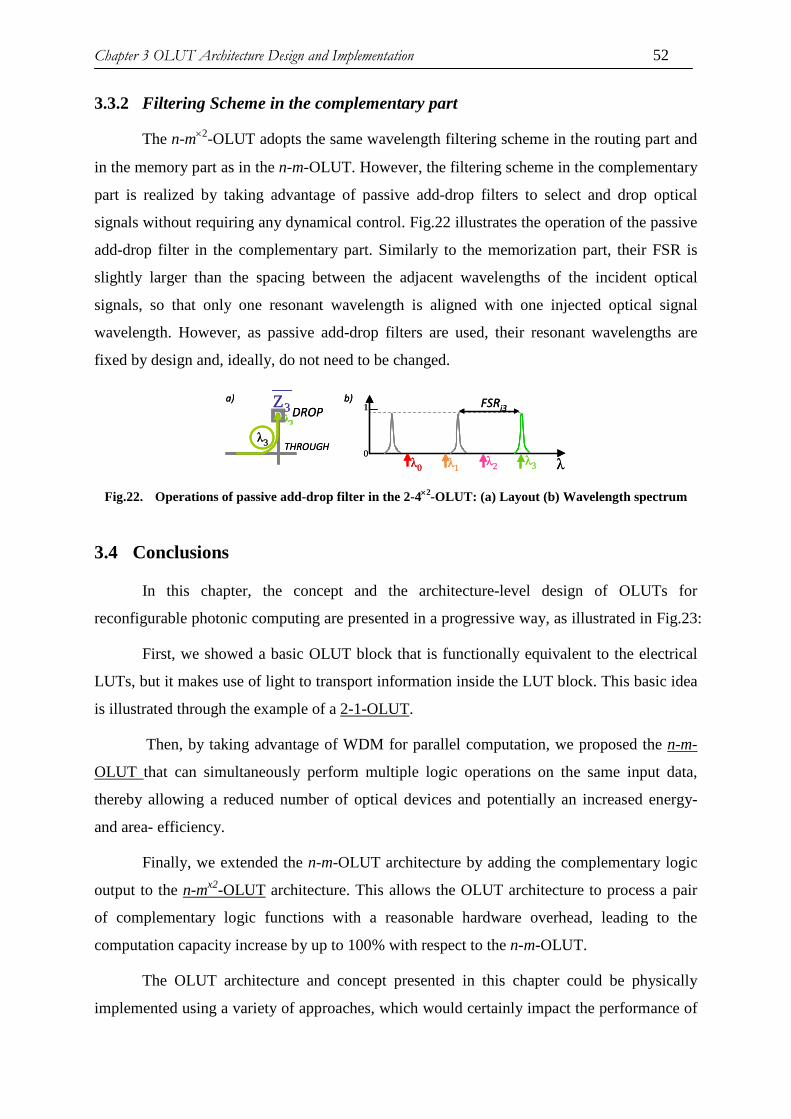
Chapter 3 OLUT Architecture Design and Implementation 52
3.3.2 Filtering Scheme in the complementary part
The n-m×2-OLUT adopts the same wavelength filtering scheme in the routing part and
in the memory part as in the n-m-OLUT. However, the filtering scheme in the complementary
part is realized by taking advantage of passive add-drop filters to select and drop optical
signals without requiring any dynamical control. Fig.22 illustrates the operation of the passive
add-drop filter in the complementary part. Similarly to the memorization part, their FSR is
slightly larger than the spacing between the adjacent wavelengths of the incident optical
signals, so that only one resonant wavelength is aligned with one injected optical signal
wavelength. However, as passive add-drop filters are used, their resonant wavelengths are
fixed by design and, ideally, do not need to be changed.
λλ0 λ1 λ2 λ3
1
0
DFSRi33Z
THROUGH
a) b)
λ3
λ3
DROP
λλ0 λ1 λ2 λ3
1
0
DFSRi33Z
THROUGH
a) b)
λ3
λ3
DROP
Fig.22. Operations of passive add-drop filter in the 2-4×2-OLUT: (a) Layout (b) Wavelength spectrum
3.4 Conclusions
In this chapter, the concept and the architecture-level design of OLUTs for
reconfigurable photonic computing are presented in a progressive way, as illustrated in Fig.23:
First, we showed a basic OLUT block that is functionally equivalent to the electrical
LUTs, but it makes use of light to transport information inside the LUT block. This basic idea
is illustrated through the example of a 2-1-OLUT.
Then, by taking advantage of WDM for parallel computation, we proposed the n-m-
OLUT that can simultaneously perform multiple logic operations on the same input data,
thereby allowing a reduced number of optical devices and potentially an increased energy-
and area- efficiency.
Finally, we extended the n-m-OLUT architecture by adding the complementary logic
output to the n-mx2-OLUT architecture. This allows the OLUT architecture to process a pair
of complementary logic functions with a reasonable hardware overhead, leading to the
computation capacity increase by up to 100% with respect to the n-m-OLUT.
The OLUT architecture and concept presented in this chapter could be physically
implemented using a variety of approaches, which would certainly impact the performance of
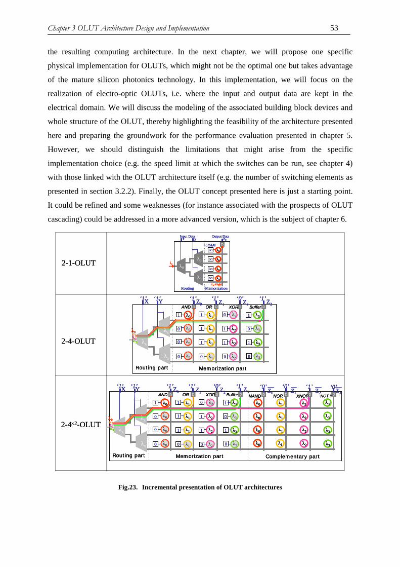
Chapter 3 OLUT Architecture Design and Implementation 53
the resulting computing architecture. In the next chapter, we will propose one specific
physical implementation for OLUTs, which might not be the optimal one but takes advantage
of the mature silicon photonics technology. In this implementation, we will focus on the
realization of electro-optic OLUTs, i.e. where the input and output data are kept in the
electrical domain. We will discuss the modeling of the associated building block devices and
whole structure of the OLUT, thereby highlighting the feasibility of the architecture presented
here and preparing the groundwork for the performance evaluation presented in chapter 5.
However, we should distinguish the limitations that might arise from the specific
implementation choice (e.g. the speed limit at which the switches can be run, see chapter 4)
with those linked with the OLUT architecture itself (e.g. the number of switching elements as
presented in section 3.2.2). Finally, the OLUT concept presented here is just a starting point.
It could be refined and some weaknesses (for instance associated with the prospects of OLUT
cascading) could be addressed in a more advanced version, which is the subject of chapter 6.
2-4×2-OLUT
2-4-OLUT
2-1-OLUT
y z0
λ0
λ0
λ0
λ0
Dλ00/1
xInput Data Output Data
SRAM
λ0 stageRouting Memorization
λ00/1
λ00/1
λ00/1
YX
1
Routing part Memorization part
1
1 1
1
1
0
0 1
0
0
0
1
0
λx
λx
D D D D
λ0
λ0
λ0
λ0
λ1
λ1
λ1
λ1 λ2
λ2
λ2
λ2
λ3
0 λ3
λ3
0 λ3
AND OR XOR Buffer
λ0λ1λ2λ3
Z0 Z1 Z2 Z3‘1’ ‘1’ ‘1’ ‘1’ ‘1’‘0’
λx
YX
1
Routing part Memorization part
1
1 1
1
1
0
0 1
0
0
0
1
0
λx
λx
D D D D
λ0
λ0
λ0
λ0
λ1
λ1
λ1
λ1 λ2
λ2
λ2
λ2
λ3
0 λ3
λ3
0 λ3
AND OR XOR Buffer
λ0λ1λ2λ3
Z0 Z1 Z2 Z3‘1’ ‘1’ ‘1’ ‘1’ ‘1’‘0’
λx
D D D D
λ0
λ1
λ1
λ1
λ2
λ2 λ3
λ3
λ0
λ0
λ0 λ1
λ2
λ2 λ3
λ3
‘0’‘0’‘0’ ‘1’2Z 3Z1Z0Z
NAND NOR XNOR NOT Y
Complementary part
2-4×2-OLUT
2-4-OLUT
2-1-OLUT
y z0
λ0
λ0
λ0
λ0
Dλ00/1
xInput Data Output Data
SRAM
λ0 stageRouting Memorization
λ00/1
λ00/1
λ00/1
y z0
λ0
λ0
λ0
λ0
Dλ00/1 λ00/1
xInput Data Output Data
SRAM
λ0 stageRouting Memorization
λ00/1 λ00/1
λ00/1 λ00/1
λ00/1 λ00/1
YX
1
Routing part Memorization part
1
1 1
1
1
0
0 1
0
0
0
1
0
λx
λx
D D D D
λ0
λ0
λ0
λ0
λ1
λ1
λ1
λ1 λ2
λ2
λ2
λ2
λ3
0 λ3
λ3
0 λ3
AND OR XOR Buffer
λ0λ1λ2λ3
Z0 Z1 Z2 Z3‘1’ ‘1’ ‘1’ ‘1’ ‘1’‘0’
λx
YX
1
Routing part Memorization part
1
1 1
1
1
0
0 1
0
0
0
1
0
λx
λx
D D D D
λ0
λ0
λ0
λ0
λ1
λ1
λ1
λ1 λ2
λ2
λ2
λ2
λ3
0 λ30 λ3
λ3
0 λ30 λ3
AND OR XOR Buffer
λ0λ1λ2λ3
Z0 Z1 Z2 Z3‘1’ ‘1’ ‘1’ ‘1’ ‘1’‘0’
λx
YX
1
Routing part Memorization part
1
1 1
1
1
0
0 1
0
0
0
1
0
λx
λx
D D D D
λ0
λ0
λ0
λ0
λ1
λ1
λ1
λ1 λ2
λ2
λ2
λ2
λ3
0 λ3
λ3
0 λ3
AND OR XOR Buffer
λ0λ1λ2λ3
Z0 Z1 Z2 Z3‘1’ ‘1’ ‘1’ ‘1’ ‘1’‘0’
λx
D D D D
λ0
λ1
λ1
λ1
λ2
λ2 λ3
λ3
λ0
λ0
λ0 λ1
λ2
λ2 λ3
λ3
‘0’‘0’‘0’ ‘1’2Z 3Z1Z0Z
NAND NOR XNOR NOT Y
Complementary part
YX
1
Routing part Memorization part
1
1 1
1
1
0
0 1
0
0
0
1
0
λx
λx
D D D D
λ0
λ0
λ0
λ0
λ1
λ1
λ1
λ1 λ2
λ2
λ2
λ2
λ3
0 λ30 λ3
λ3
0 λ30 λ3
AND OR XOR Buffer
λ0λ1λ2λ3
Z0 Z1 Z2 Z3‘1’ ‘1’ ‘1’ ‘1’ ‘1’‘0’
λx
D D D D
λ0
λ1
λ1
λ1
λ2
λ2 λ3
λ3
λ0
λ0
λ0 λ1
λ2
λ2 λ3
λ3
‘0’‘0’‘0’ ‘1’2Z 3Z1Z0Z
NAND NOR XNOR NOT Y
Complementary part
Fig.23. Incremental presentation of OLUT architectures

Chapter 3 OLUT Architecture Design and Implementation 54

Chapter 4 From architecture to device: multi-level modelling and simulation 55
Chapter 4 FROM ARCHITECTURE TO DEVICE: MULTI-LEVEL MODELLING AND SIMULATION
This chapter deals with the technological aspects required to practically implement the
OLUT introduced in Chapter 3 and addresses the following questions: How can we properly
design its constituent building blocks using a mature silicon photonics technology? How can
we achieve the required system performance when these building blocks are integrated in
OLUT architectures?
A multi-level modeling approach including both the physical and system aspects is
required for investigating the full potential and performance of OLUTs. At the physical level,
we model the behavior of photonic devices using analytical tools such as Coupled Mode
Theory [131] and commercial tools, such as RSoft FDTD and multiphysics utility software
[127]. The device metrics (e.g. transmission, geometry) are then extracted to describe the
system behavior of the resulting OLUT. This model also allows the estimation of the required
optical laser power to ensure a certain level of performance for the OLUT system, e.g. a given
BER at all outputs. This model will allow us to explore the design space of the silicon
photonic devices for performing reliable and energy-efficient computation in OLUT
architectures, as detailed in Chapter 5.
The chapter is organized as follows. Section 4.1 provides an overview of the basic
functional toolbox relying on silicon photonics technology for implementing OLUTs, such as
micro-lasers, photodetectors, waveguides and add-drop filters. In section 4.2, we discuss in
further detail the design of the electro-optic add-drop filters using optical modeling and
electrical simulations. Additionally, different schemes for electrically controlling these add-
drop filters are investigated. Section 4.3 focuses on system level aspects, in particular the
impact of system-level parameters, i.e. the BER, and the OLUT dimensions, on the design of
the devices that are needed to implement the system efficiently. We investigate the optical
losses associated with the silicon photonic layout, and build the energy model for estimating
the total energy consumption in the OLUT system.
Chapter 4 From architecture to device: multi-level modelling and simulation 56
4.1 Functional toolbox based on silicon photonics for implementing OLUT
The OLUT has the potential to make the most of silicon photonics through WDM,
thereby allowing parallel computation. This requires wavelength selective optical components
to route and filter different wavelength channels according to the control signal. The most
compact way to implement such function is to use a resonator-based add-drop filter, for
instance made of a microring resonator (Fig.24 a) [139,115]. In this chapter, we describe a
physical implementation of the electro-optic OLUT that can be realized using a mature
photonics technology. This implies an electrical bias voltage to be used as the control signal
of the microring based add-drop filter. Electrically-controlled silicon microring resonators are
commonly used in optical interconnects and optical computing architectures, since they
combine the key characteristics for such applications, i.e. i) a ten-to-hundred µm-scale
footprint ii) Gigabit/s data rate iii) picosecond transmission delay (latency), iv) low switching
energy (e.g. ~1fJ/bit [170]), and v) large-scale integration for on-chip photonic applications.
We adopt these devices as the essential switching elements for OLUTs.
Alternatively, it is possible to implement these optical switching elements with two-
path interference structures such as Mach-Zehnder interferometers, but their physical size
might be too large to be integrated on a chip at a large scale, as compared with compact ring
resonator based devices. In this section, we introduce all the optical building blocks of
OLUTs, with a strong emphasis on the add-drop filter for which we first establish the
transmission model in the passive regime.
4.1.1 Passive Add-Drop Filters (Microring resonator)
4.1.1.1 Basic Principles
Basically, the SOI-based add-drop filter that we choose to use in OLUTs is a silicon
microring resonator side-coupled to two crossing waveguides. A schematic is shown in Fig.24
a) and the associated transmission response is displayed in Fig.24 (b). It exhibits a spectral
comb of regularly spaced resonance peaks (each peak is typically a Lorentzian-shape function,
and their spacing is related to Free Spectral Range (FSR)), and each of the resonance
wavelengths could serve as a filtering channel for the data input (Fig.24 (b)) [153]. We next
focus on one specific resonance wavelength and its closest signal wavelength. As presented
before (see section 3.1), the add-drop filter acts as an optical router or an optical switch
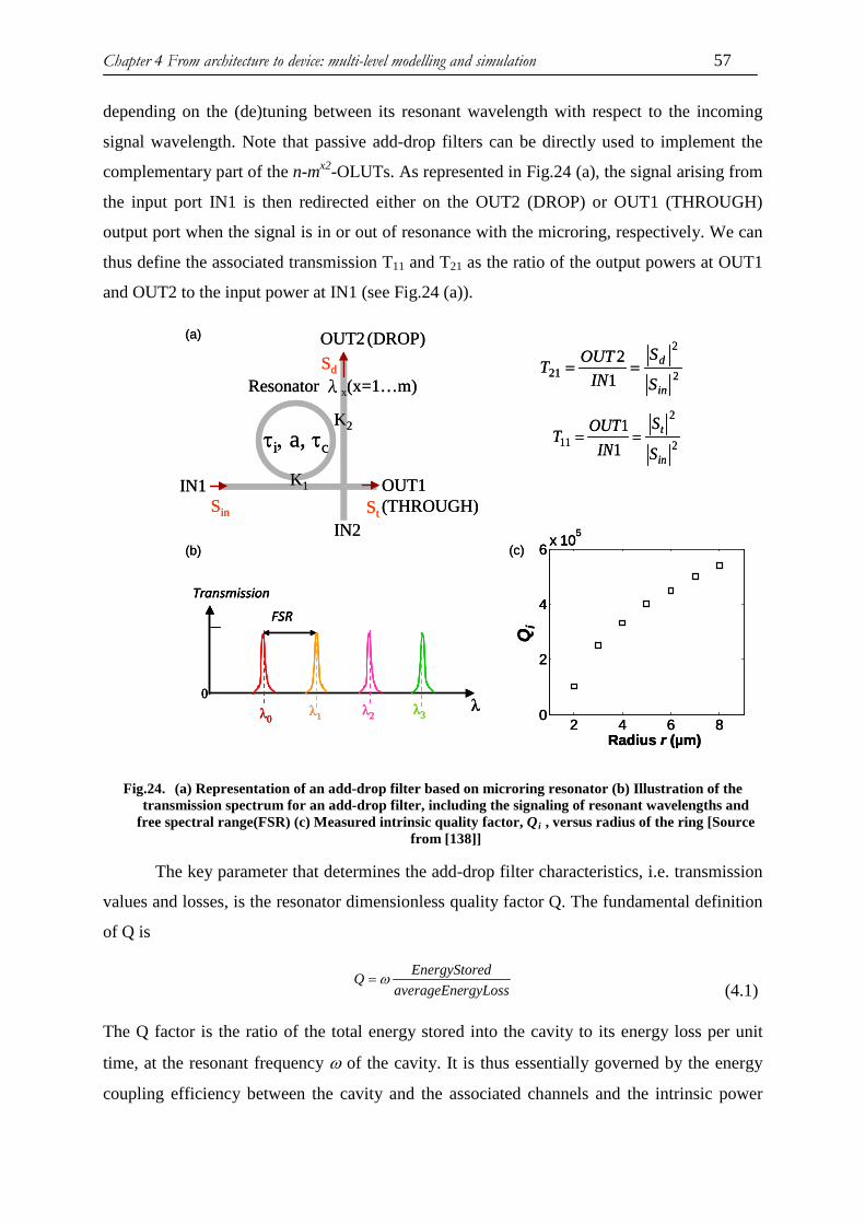
Chapter 4 From architecture to device: multi-level modelling and simulation 57
depending on the (de)tuning between its resonant wavelength with respect to the incoming
signal wavelength. Note that passive add-drop filters can be directly used to implement the
complementary part of the n-mx2-OLUTs. As represented in Fig.24 (a), the signal arising from
the input port IN1 is then redirected either on the OUT2 (DROP) or OUT1 (THROUGH)
output port when the signal is in or out of resonance with the microring, respectively. We can
thus define the associated transmission T11 and T21 as the ratio of the output powers at OUT1
and OUT2 to the input power at IN1 (see Fig.24 (a)).
IN1Sin St
Sd
ti, a, tc
(DROP)
IN2
Resonator λx(x=1…m)
2
2
11 11
in
t
S
SIN
OUTT ==
2
2
21 12
in
d
S
SIN
OUTT ==
OUT2
OUT1 (THROUGH)
FSR
λλ0λ1 λ2 λ3
0
Transmission
(a)
(b)
K1
Qi
Radius r (µm)2 4 6 8
0
2
4
6 x 10⁵
K2
(c)
IN1Sin St
Sd
ti, a, tc
(DROP)
IN2
Resonator λx(x=1…m)
2
2
11 11
in
t
S
SIN
OUTT ==
2
2
21 12
in
d
S
SIN
OUTT ==
OUT2
OUT1 (THROUGH)
FSR
λλ0λ1 λ2 λ3
0
Transmission
FSR
λλ0λ1 λ2 λ3
0
Transmission
(a)
(b)
K1
Qi
Radius r (µm)2 4 6 8
0
2
4
6 x 10⁵Q
i
Radius r (µm)2 4 6 8
0
2
4
6 x 10⁵
K2
(c)
Fig.24. (a) Representation of an add-drop filter based on microring resonator (b) Illustration of the transmission spectrum for an add-drop filter, including the signaling of resonant wavelengths and
free spectral range(FSR) (c) Measured intrinsic quality factor, Qi , versus radius of the ring [Source from [138]]
The key parameter that determines the add-drop filter characteristics, i.e. transmission
values and losses, is the resonator dimensionless quality factor Q. The fundamental definition
of Q is
rgyLossaverageEneedEnergyStorQ ω=
(4.1)
The Q factor is the ratio of the total energy stored into the cavity to its energy loss per unit
time, at the resonant frequency ω of the cavity. It is thus essentially governed by the energy
coupling efficiency between the cavity and the associated channels and the intrinsic power

Chapter 4 From architecture to device: multi-level modelling and simulation 58
loss within the cavity (associated with an intrinsic Q factor), which typically depends on the
cavity geometry and roughness induced scattering for a given material platform and
technology like silicon photonics [138][153]. Fig.24 (c) plots an estimation of the intrinsic
quality factor (excluding coupling loss) as a function of the radius of the microring based on
experimental data from [138]. Since a microring resonator has an additional surface that can
induce more scattering loss than the microdisk resonator, the experimental values of intrinsic
quality factor associated with a microdisk resonator extracted from [138] are divided by a
factor of two2 for the ring resonator, to produce the estimated data of Fig.24 (c). This curve
will be used in the performance evaluation of the next chapter to account for the experimental
trend of decreasing losses for larger microrings.
A high Q cavity allows for slower loss rate, thus achieving a stronger resonant effect.
If t represents the decay time of the electric field amplitude A(t) of an optical mode in the
resonator (i.e. A (t) varies as tt
e−
), Equation (4.1) gives:
2/ωt=Q (4.2)
In the transmission spectrums presented in Fig.24(b), the ratio between the resonant
wavelength λ0 (transmission peak) and the Q factor (λ0/Q) is the full spectral width at half
maximum (FWHM)δλ , i.e. Q/0λδλ = . Hence, the resonant wavelength and the Q factor fully
describe the add-drop filter response close to one resonance. In the following, we express the
resonator transmission as a function of the Q-factor and the wavelength shift, using the
Coupled Mode Theory (CMT [131]) in time.
4.1.1.2 Passive add-drop filter transmission and Coupled Mode Theory
We now derive the add-drop filter transmissions as a function of the Q factor and
wavelength detuning between the incoming signal and the microring resonance. For this, we
directly use the set of equations describing the coupling of the cavity and the two waveguides
according to the temporal Coupled Mode Theory (CMT). The derivation of these equations
can be found in many references and books (see [131, 132][144] [145] [153]) and we will not
fully detail them here.
2 This factor is a rough estimation for the ring. It is optimistic if two horizontal surfaces of the ring are taken into account.
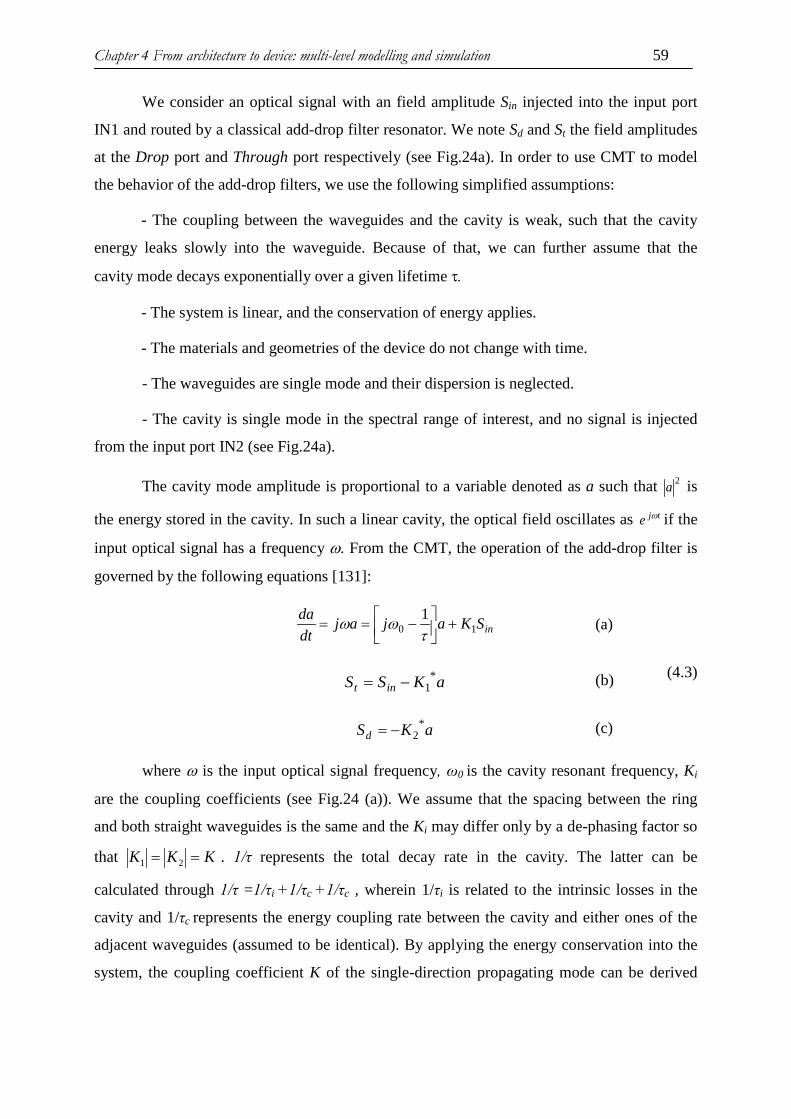
Chapter 4 From architecture to device: multi-level modelling and simulation 59
We consider an optical signal with an field amplitude Sin injected into the input port
IN1 and routed by a classical add-drop filter resonator. We note Sd and St the field amplitudes
at the Drop port and Through port respectively (see Fig.24a). In order to use CMT to model
the behavior of the add-drop filters, we use the following simplified assumptions:
- The coupling between the waveguides and the cavity is weak, such that the cavity
energy leaks slowly into the waveguide. Because of that, we can further assume that the
cavity mode decays exponentially over a given lifetime t.
- The system is linear, and the conservation of energy applies.
- The materials and geometries of the device do not change with time.
- The waveguides are single mode and their dispersion is neglected.
- The cavity is single mode in the spectral range of interest, and no signal is injected
from the input port IN2 (see Fig.24a).
The cavity mode amplitude is proportional to a variable denoted as a such that 2a is
the energy stored in the cavity. In such a linear cavity, the optical field oscillates as tje ω if the
input optical signal has a frequency ω. From the CMT, the operation of the add-drop filter is
governed by the following equations [131]:
inSKajaj
dtda
101
+
−==
tωω (a)
(4.3) aKSS int
*1−= (b)
aKSd*
2−= (c)
where ω is the input optical signal frequency, ω0 is the cavity resonant frequency, Ki
are the coupling coefficients (see Fig.24 (a)). We assume that the spacing between the ring
and both straight waveguides is the same and the Ki may differ only by a de-phasing factor so
that KKK == 21 . 1/τ represents the total decay rate in the cavity. The latter can be
calculated through 1/τ =1/τi +1/τc +1/τc , wherein 1/τi is related to the intrinsic losses in the
cavity and 1/τc represents the energy coupling rate between the cavity and either ones of the
adjacent waveguides (assumed to be identical). By applying the energy conservation into the
system, the coupling coefficient K of the single-direction propagating mode can be derived

Chapter 4 From architecture to device: multi-level modelling and simulation 60
asct2 . The absolute squared value of this coupling coefficient (2/τc) is equal to the total rate
of power decay from the cavity into both adjacent waveguides. The optical power
transmission at the Through port and the Drop port is defined as T11=|St|2/|Sin|2 and
T21=|Sd|2/|Sin|2. To solve for these transmission variables, we divide Equation (4.3)(b) and
Equation (4.3) (c) by Sin and then substitute a from Equation (4.3) (a). We obtain the
transmissions in the stationary state:
2
02
2
21
2
02
2
11
1)(
2
1)(
2
1
tωω
t
tωω
t
+−==
+−−==
jS
ST
jS
ST
c
in
d
c
in
t
(4.4)
This then yields:
22
0
2
2
2
21
22
0
22
2
2
11
1)(
4
1)(
)21(1
1
tωω
t
tωω
ttt
+−==
+−
−−
−==
c
c
in
d
in
t
S
ST
S
ST
(4.5)
Equation (4.5) gives a Lorentzian shape for both transmission values with a maximum
at ω=ω0 for the Drop port and a minimum value for the Through port, i.e. when the incoming
signal is spectrally aligned with the microring resonance. Commonly, it is useful to write the
above transmission equations using Q factors for describing the various loss contributions.
Using the relation (4.2) and converting the angular frequencies into wavelengths, we finally
obtain:
[ ]
[ ] 1/2)/2(
1/2)/21(11
2
2
21
2
2
11
+∆=
+∆
−−−=
λλ
λλ
L
cL
L
cL
QQQT
QQQT
(4.6)
Where ∆λ is the difference between the input wavelength and the closest resonance
wavelength, QL is the total quality factor of the ring cavity (QL = ωt/2) and Qc is the coupling
quality factor associated with the coupling rate into one waveguide (Qc = ωtc/2 ). QL can be

Chapter 4 From architecture to device: multi-level modelling and simulation 61
calculated through 111 2 −−− += icL QQQ , wherein Qi is the intrinsic quality factor limited by the
scattering losses in the ring (Qi = ωti/2 ), which typically depends on the ring radius as
illustrated in Fig.24 (c).
From Equation (4.6), when the add-drop filter is in the Drop state (on-resonance state
i.e. ∆λ=0), we can infer that the transmissions at the Through and the Drop ports are 2
11 )/21( cL QQT −= and 221 )/2( cL QQT = . If we assume the ring scattering loss is negligible
(Qi >>Qc), it then follows that 11 2 −− = cL QQ , resulting in the ideal and targeted values of
transmissions T21= 1 and T11= 0 for the Drop (on-resonance) state. In these conditions,
without any other loss (e.g. free-space scattering or absorption), the transmission peak T11 can
reach 100%. Additional loss contributions result in a decrease of Qi, thus degrading this
transmission peak.
A special case study: an optical signal is injected from port IN2
For completeness, we consider the case where the optical signal is injected from the
input port IN2 of the microring add-drop filter, which occurs in a given column of the
memorization stage of the n-m-OLUT for the signal arising from another add-drop filter in the
Drop state. Indeed, the memorization stage is built such that all the add-drop filters of a given
column have the same resonant wavelength (see Fig.14 in chapter 3). In this scenario, if the
add-drop filter resonance λx is aligned with the wavelength of the incoming light λi, the
optical signal will couple into the ring from IN2 and be redirected into the horizontal
waveguide, thereby exiting from the OUT1 port. Fig.25 shows the result of an FDTD
simulation describing this scenario. This situation should be avoided in the memorization part
of the OLUT, since it would almost fully attenuate the signal coming from the downside,
thereby generating a logic ‘0’ instead of a logic '1' at the output of the associated
photodetector. This issue can however be solved by using the layout represented in Fig.26. In
this scheme, both an individual vertical waveguide and photodetector are assigned to each
add-drop filter of one given column, and these add-drop filters are horizontally shifted with
respect to one another instead of being vertically aligned. The vertical outputs of the add-drop
filters of one given column are subsequently merged in the electrical domain to provide the
intended Z0 logic value. In principle, this could be done without adding much optical loss
apart from the contribution of the additional crossing points (considering that several design
solutions exist for reducing the waveguide crossing losses) nor energy consumption since
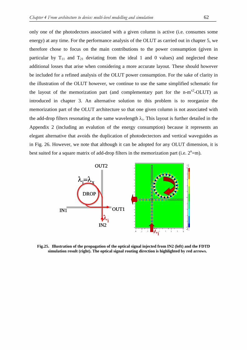
Chapter 4 From architecture to device: multi-level modelling and simulation 62
only one of the photodectors associated with a given column is active (i.e. consumes some
energy) at any time. For the performance analysis of the OLUT as carried out in chapter 5, we
therefore chose to focus on the main contributions to the power consumption (given in
particular by T11 and T21 deviating from the ideal 1 and 0 values) and neglected these
additional losses that arise when considering a more accurate layout. These should however
be included for a refined analysis of the OLUT power consumption. For the sake of clarity in
the illustration of the OLUT however, we continue to use the same simplified schematic for
the layout of the memorization part (and complementary part for the n-mx2-OLUT) as
introduced in chapter 3. An alternative solution to this problem is to reorganize the
memorization part of the OLUT architecture so that one given column is not associated with
the add-drop filters resonating at the same wavelength λi. This layout is further detailed in the
Appendix 2 (including an evalution of the energy consumption) because it represents an
elegant alternative that avoids the duplication of photodectectors and vertical waveguides as
in Fig. 26. However, we note that although it can be adopted for any OLUT dimension, it is
best suited for a square matrix of add-drop filters in the memorization part (i.e. 2n=m).
DROP
IN1
IN2
OUT1
OUT2
λi=λx
λi
λi
DROP
IN1
IN2
OUT1
OUT2
λi=λx
λi
λi
Fig.25. Illustration of the propagation of the optical signal injected from IN2 (left) and the FDTD simulation result (right). The optical signal routing direction is highlighted by red arrows.
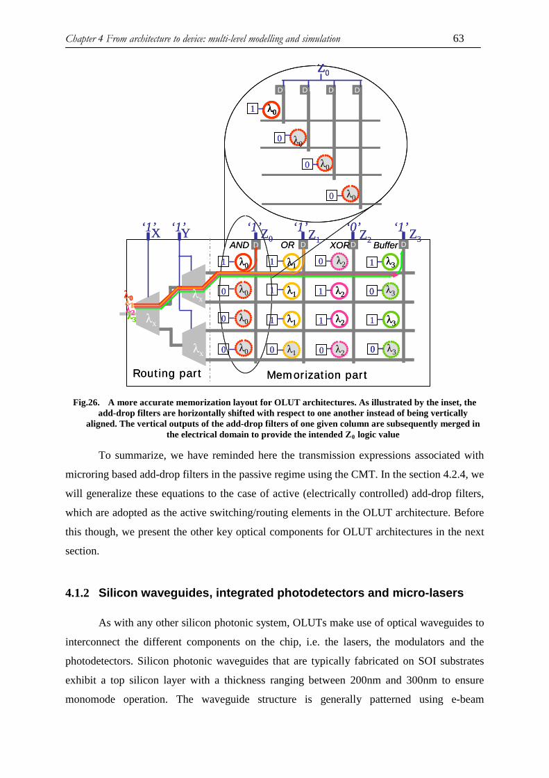
Chapter 4 From architecture to device: multi-level modelling and simulation 63
YX
1
Routing part Memorization part
1
1 1
1
1
0
0 1
0
0
0
1
0
λx
λx
D D D D
λ0
λ0
λ0
λ0
λ1
λ1
λ1
λ1 λ2
λ2
λ2
λ2
λ3
0 λ3
λ3
0 λ3
AND OR XOR Buffer
λ0λ1λ2λ3
Z0 Z1 Z2 Z3‘1’ ‘1’ ‘1’ ‘1’ ‘1’‘0’
λx
λ0
λ0
λ0
λ0
D D D D
Z0
1
0
0
0
YX
1
Routing part Memorization part
1
1 1
1
1
0
0 1
0
0
0
1
0
λx
λx
D D D D
λ0
λ0
λ0
λ0
λ1
λ1
λ1
λ1 λ2
λ2
λ2
λ2
λ3
0 λ30 λ3
λ3
0 λ30 λ3
AND OR XOR Buffer
λ0λ1λ2λ3
Z0 Z1 Z2 Z3‘1’ ‘1’ ‘1’ ‘1’ ‘1’‘0’
λx
λ0
λ0
λ0
λ0
D D D D
Z0
λ0
λ0
λ0
λ0
D D D D
Z0
1
0
0
0
Fig.26. A more accurate memorization layout for OLUT architectures. As illustrated by the inset, the add-drop filters are horizontally shifted with respect to one another instead of being vertically
aligned. The vertical outputs of the add-drop filters of one given column are subsequently merged in the electrical domain to provide the intended Z0 logic value
To summarize, we have reminded here the transmission expressions associated with
microring based add-drop filters in the passive regime using the CMT. In the section 4.2.4, we
will generalize these equations to the case of active (electrically controlled) add-drop filters,
which are adopted as the active switching/routing elements in the OLUT architecture. Before
this though, we present the other key optical components for OLUT architectures in the next
section.
4.1.2 Silicon waveguides, integrated photodetectors and micro-lasers
As with any other silicon photonic system, OLUTs make use of optical waveguides to
interconnect the different components on the chip, i.e. the lasers, the modulators and the
photodetectors. Silicon photonic waveguides that are typically fabricated on SOI substrates
exhibit a top silicon layer with a thickness ranging between 200nm and 300nm to ensure
monomode operation. The waveguide structure is generally patterned using e-beam
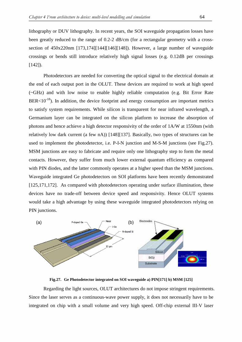
Chapter 4 From architecture to device: multi-level modelling and simulation 64
lithography or DUV lithography. In recent years, the SOI waveguide propagation losses have
been greatly reduced to the range of 0.2-2 dB/cm (for a rectangular geometry with a cross-
section of 450x220nm [173,174][144][146][148]). However, a large number of waveguide
crossings or bends still introduce relatively high signal losses (e.g. 0.12dB per crossings
[142]).
Photodetectors are needed for converting the optical signal to the electrical domain at
the end of each output port in the OLUT. These devices are required to work at high speed
(~GHz) and with low noise to enable highly reliable computation (e.g. Bit Error Rate
BER<10-18). In addition, the device footprint and energy consumption are important metrics
to satisfy system requirements. While silicon is transparent for near infrared wavelength, a
Germanium layer can be integrated on the silicon platform to increase the absorption of
photons and hence achieve a high detector responsivity of the order of 1A/W at 1550nm (with
relatively low dark current (a few nA)) [148][137]. Basically, two types of structures can be
used to implement the photodetector, i.e. P-I-N junction and M-S-M junctions (see Fig.27).
MSM junctions are easy to fabricate and require only one lithography step to form the metal
contacts. However, they suffer from much lower external quantum efficiency as compared
with PIN diodes, and the latter commonly operates at a higher speed than the MSM junctions.
Waveguide integrated Ge photodetectors on SOI platforms have been recently demonstrated
[125,171,172]. As compared with photodetectors operating under surface illumination, these
devices have no trade-off between device speed and responsivity. Hence OLUT systems
would take a high advantage by using these waveguide integrated photodetectors relying on
PIN junctions.
(a) (b)(a) (b)
Fig.27. Ge Photodetector integrated on SOI waveguide a) PIN[171] b) MSM [125]
Regarding the light sources, OLUT architectures do not impose stringent requirements.
Since the laser serves as a continuous-wave power supply, it does not necessarily have to be
integrated on chip with a small volume and very high speed. Off-chip external III-V laser
Chapter 4 From architecture to device: multi-level modelling and simulation 65
diodes that deliver sufficient output optical power (which will be clarified in the section
4.3.3.4) and well-controlled emitting wavelength are well-suited for OLUTs.
4.2 Design of active add-drop filters for OLUT architectures
We next introduce and discuss our choice to implement the electro-optic add-drop
filters that represent the main active components for the OLUT architecture proposed in
section 3.1.
4.2.1 Electrically-controlled modulation of an optical signal
By applying an external electrical signal (voltage) onto a dielectric material such as
silicon, the amplitude and the phase of an optical signal can be modulated. More specifically,
the optical signal that propagates into a silicon waveguide can be modulated by changing the
refractive index of silicon, i.e. its real part or its imaginary part. The imaginary part of the
refractive index can be changed through the electro-absorption effect, but this affects the
intensity of the light that goes through by introducing additional optical losses, so that it is not
energy conservative. In contrast, the modulation of the real part of the refractive index
directly impacts the phase of the incident light, and together with an appropriate structure
(such as a microring resonator or a Mach-Zehnder interferometer), it can be turned into a
wavelength selective approach for modulating the intensity of the optical signal.
Practically, three possible ways can be used to tune the real part of the refractive index:
the thermo-optic effect, the electro-optic effect and the free-carrier induced electro-refractive
effect. As summarized in Tab 2, these effects have different modulation strengths and time
response: the electro-optic effect is the fastest effect but it has a limited tuning range; the
thermo-optic effect is the strongest but is very slow; the response time and the modulation
strength of the electro-refractive effect are in between. In the OLUT architecture, the add-drop
filters in the memorization part and the routing part have different constraints: the first ones
could use the thermo-optic effect since we do not need them to be fast, while the second ones
could make use of the electro-refractive effect because of the required high operation speed.
We next briefly introduce the electro-optic mechanism and then present the other two
mechanisms in further detail as these are considered for the OLUT implementation.
Tab 2. Different mechanisms for electrically-controlled optical modulation with typical values for tuning range, response time, power efficiency and energy consumption

Chapter 4 From architecture to device: multi-level modelling and simulation 66
Thermo-optic
effect
Electro-optic
effect
Electro-
refractive effect
Typical tuning
range
~ 10 nm ~0.1nm[168] ~ nm
Typical response
time
~µs ~10 ps ~ns
Typical power
efficiency
1mW/nm [167]
3.5mW/nm [154]
N/A 1mW/nm [137]
Typical energy
consumption
~1 pJ/bit [167]
~2 pJ/bit [154]
N/A 85fJ/bit [137]
300fJ/bit [165]
4.2.1.1 Electro-optic effect
The optical properties of several dielectric materials can be changed by applying an
electric field (either a voltage or an optical signal). Common electro-optic effects used in
semiconductor materials include the Pockels effect and the Kerr effect. However, due to the
central-symmetric lattice, crystalline silicon does not exhibit the Pockels effect unless the
symmetry of the lattice is broken [115]. The electro-optic Kerr effect in silicon can be very
fast, since it involves a near instantaneous response of the bound electrons in the material, but
is much weaker than the other ones in Si.
4.2.1.2 Thermo-optic effect
The thermo-optic effect causes a wavelength red-shift upon increasing temperature
due to an associated rise of the refractive index. Considering the temperature sensitivity of the
refractive index in silicon that is given by 14108.1/ −−×= KdTdn at room temperature, a change
of refractive index of 0.001 can be achieved by increasing the device temperature by 6°C. The
reverse direction i.e. cooling effect is also possible but is even slower. The thermo-optic effect
is one of the commonly applied approaches for providing static control of the resonant
wavelength in the microring based add-drop filters. It can shift the wavelength spectrum by up
to more than 10 nanometers, depending on the geometry of the microring resonator. For
example, a thermal tuning range of more than 10nm with a heating efficiency of 28µW/GHz
has been demonstrated in silicon microring resonators with a radius of 7µm (16nm FSR) [154]

Chapter 4 From architecture to device: multi-level modelling and simulation 67
(Fig.28). The thermo-optic effect can be obtained by simply applying an electric current to a
micro-heater integrated onto or inside the device region. As illustrated in Fig.29, it can be
realized by putting metallic resistors on top of the device claddings [146], or by heating the
silicon device through doped/silicided resistors [147], or by directly integrating the heater
inside the core of a silicon waveguide [148].
In OLUTs, the thermo-optic effect is typically needed to align the initial resonances of
the ring resonators with respect to the incoming signal wavelengths in a step referred to as a
“pre-calibration”. This would compensate for the fabrication inaccuracy of the microring, and
stabilize the initial OLUT configuration (i.e. configure the state of the add-drop filters in the
memorization part when the RAM value is applied). Some approaches are possible to reduce
the temperature drift, e.g. incorporating the cladding material with a temperature dependency
that is opposite to silicon [115]. However, they are not CMOS compatible at the current stage.
It is also possible to improve the temperature stabilization through the use of higher order
rings (i.e. cascading multiple rings), but the device complexity, footprint and power
consumption will be disadvantageously increased [164].
Fig.28. Microring resonator with integrated heater structure [154]
Waveguide coreBuried oxide
Silicon substrate
Silicon wireTop oxide cladding
Metal resistor
Heating current
Silicon waveguide
Waveguide coreBuried oxide
Silicon substrate
Silicon wireTop oxide cladding
Metal resistor
Heating current
Silicon waveguide
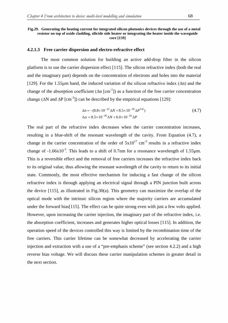
Chapter 4 From architecture to device: multi-level modelling and simulation 68
Fig.29. Generating the heating current for integrated silicon photonics devices through the use of a metal resistor on top of oxide cladding, silicide side heater or integrating the heater inside the waveguide
core [159]
4.2.1.3 Free carrier dispersion and electro-refractive effect
The most common solution for building an active add-drop filter in the silicon
platform is to use the carrier dispersion effect [115]. The silicon refractive index (both the real
and the imaginary part) depends on the concentration of electrons and holes into the material
[129]. For the 1.55µm band, the induced variation of the silicon refractive index (∆n) and the
change of the absorption coefficient (∆α [cm-1]) as a function of the free carrier concentration
change (∆N and ∆P [cm-3]) can be described by the empirical equations [129]:
PN
PNn
∆×+∆×=∆
∆×+∆×−=∆−−
−−
1818
8.01822
100.6105.8
)105.8108.8(
α (4.7)
The real part of the refractive index decreases when the carrier concentration increases,
resulting in a blue-shift of the resonant wavelength of the cavity. From Equation (4.7), a
change in the carrier concentration of the order of 5x1017 cm-3 results in a refractive index
change of -1.66x10⁻³. This leads to a shift of 0.7nm for a resonance wavelength of 1.55µm.
This is a reversible effect and the removal of free carriers increases the refractive index back
to its original value, thus allowing the resonant wavelength of the cavity to return to its initial
state. Commonly, the most effective mechanism for inducing a fast change of the silicon
refractive index is through applying an electrical signal through a PIN junction built across
the device [115], as illustrated in Fig.30(a). This geometry can maximize the overlap of the
optical mode with the intrinsic silicon region where the majority carriers are accumulated
under the forward bias[115]. The effect can be quite strong even with just a few volts applied.
However, upon increasing the carrier injection, the imaginary part of the refractive index, i.e.
the absorption coefficient, increases and generates higher optical losses [115]. In addition, the
operation speed of the devices controlled this way is limited by the recombination time of the
free carriers. This carrier lifetime can be somewhat decreased by accelerating the carrier
injection and extraction with a use of a “pre-emphasis scheme” (see section 4.2.2) and a high
reverse bias voltage. We will discuss these carrier manipulation schemes in greater detail in
the next section.

Chapter 4 From architecture to device: multi-level modelling and simulation 69
(a) (b)(a) (b)
Fig.30. (a) A diagram of silicon microring resonator with a PIN junction built across the device [127] (b) Topside: the cross-section of silicon PINPIN microring resonator using a carrier depletion mecanism,
downside: the electronic microscopy diagram [163]
Alternatively, the carrier concentration can also be controlled through using the
depletion mechanism when applying a reverse bias across the electrical junction (i.e. a reverse
biased PN diode). According to [115][150][152], since the carriers are driven by voltage
depletion instead of diffusion, the associated device operation speed is not limited by the
carrier recombination time in this case, but only by the material carrier mobility and the
device capacitance. Hence, reverse biased PN diode modulators can ideally run at a higher
speed than forward biased PIN diode modulators. However, because the number of free
carriers involved in changing the refractive index is much smaller than that with the carrier
injection mechanism, the electro-refractive effect induced through carrier depletion is much
weaker. As a result, a higher bias is needed for achieving a given refractive index change.
Although this effect can be enhanced by using a more complex junction structure like PIPIN
(as shown schematically in Fig.30 (b)) that enables a better overlap of the optical mode with
the junction intrinsic zone [152] [163], these geometries are not mature enough even at the
laboratory development phase. We do not adopt this approach for the OLUT architecture
mainly because our aim is to design large-scale photonic computing systems with low power
consumption and, as fas as possible, standard integrated device technology.
Finally, it is also possible to use candidate structures other than PN junctions to
achieve the carrier dispersion effect, for instance a Schottky diodes [153], or MOS Capacitors
[153]. The first, which consists of a metal/semiconductor junction, is not considered for
OLUTs since it has a higher absorption loss induced by the metal. The second alternative is

Chapter 4 From architecture to device: multi-level modelling and simulation 70
also dismissed in this work due to the fact that it is not straightforward to make a good
capacitor for these SOI based device structure since they have a vertical insulator layer [153].
To conclude, in the OLUT architecture, both the thermo-optic and electro-refractive
effect could be used for implementing the active add-drop filters in the memorization part, but
the latter is the only viable solution for the active add-drop filters in the routing part. For the
electro-optical implementation of the OLUT architecture presented in this chapter and in next
one, we consider the use of the electro-refractive scheme for the active add-drop filters of
both the routing and the memorization part (In particular for the estimation of the OLUT
power consumption). We keep in mind though that and the thermo-optic effect would likely
be required for pre-calibration. In the next section, we briefly review the carrier manipulation
principle of a classical PIN junction that will be used in the active add-drop filters.
4.2.2 Carrier electrical manipulation with PIN junction
By applying a forward electrical bias, PIN diodes can efficiently inject free carriers
into the (central) intrinsic region of the device. When the device is powered off or a reverse
bias is applied, the free carriers recombine or are extracted out of the intrinsic silicon region.
This practically provides an electrical control of the resonant wavelength of the microring
resonator.
If the diode is driven by a current IF, the speed at which free carriers are injected into
the intrinsic region is governed by the following rate equation:
F
c
tottot Iqdt
dq+−=
t (4.8)
where τc is the carrier lifetime or average recombination time, and qtot is the total charge of
electrons or holes in the region. Supposing that the diode is initially powered off, the minority
carrier density in the intrinsic region is very low and can be neglected leading to qtot(t=0) ~0.
The solution of Equation (4.8) for a constant current IF, is then:
)1()( / ctcFtot eItq tt −−= (4.9)
In the steady state, the electrical charge is qtot=IFtc, so that higher current leads to a
higher steady-state carrier density. This relation can be seen more clearly in the left part of
Fig.31 (a) where the evolution of electrical charges versus time for varying values of IF is
plotted. In addition, by differentiating Equation (4.9) with respect to t, the carrier injection
rate is obtained to be ctF eI t/− . This rate is proportional to IF and decreases exponentially with
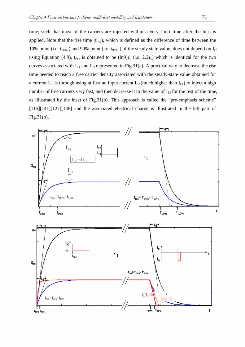
Chapter 4 From architecture to device: multi-level modelling and simulation 71
time, such that most of the carriers are injected within a very short time after the bias is
applied. Note that the rise time (trise), which is defined as the difference of time between the
10% point (i.e. t10% ) and 90% point (i.e. t90% ) of the steady state value, does not depend on IF:
using Equation (4.9), trise is obtained to be (ln9)τc (i.e. 2.2τc) which is identical for the two
curves associated with IF1 and IF2 represented in Fig.31(a). A practical way to decrease the rise
time needed to reach a free carrier density associated with the steady-state value obtained for
a current IF1 is through using at first an input current IF2 (much higher than IF1) to inject a high
number of free carriers very fast, and then decrease it to the value of IF1 for the rest of the time,
as illustrated by the inset of Fig.31(b). This approach is called the “pre-emphasis scheme”
[115][141][127][148] and the associated electrical charge is illustrated in the left part of
Fig.31(b).
t
tfall= t’10%- t’90%
t’10%t’90%
tc
t10% t90%
trise= t90%- t10%
tc
tc
qtotIF1
IF2 =3 IF1
IF2
(a)
t
IF2
IF1
t
tfall= t’10%- t’90%
t’10%t’90%
tctctc
t10% t90%
trise= t90%- t10%
tctc
tctc
qtotIF1
IF2 =3 IF1
IF2
(a)
t
IF2
IF1
tc
tc
qtot
t
IF2
IF1
t90%
t10% t90%
trise= t90%- t10%
t
tfall= t’10%- t’90%
t’10%t’90%
tc
tIF
IR
IR/IF =3IR/IF =2
(b)tctc
tctc
qtot
t
IF2
IF1
t90% t
IF2
IF1
t90%
t10% t90%
trise= t90%- t10%
t
tfall= t’10%- t’90%
t’10%t’90%
tc
tIF
IR
IR/IF =3IR/IF =2
t
tfall= t’10%- t’90%
t’10%t’90%
tctctc
tIF
IR
IR/IF =3IR/IF =2
(b)

Chapter 4 From architecture to device: multi-level modelling and simulation 72
Fig.31. Illustration of the electrical response of a PIN junction (a) Definition of rise and fall time of the output that has an exponential time dependence with the constant of carrier lifetime. (b) Charge
injected by a PIN junction when a pre-emphasis input current is applied with a reverse bias current to extract the carriers in the junction, illustrated by continuous red lines. For comparison, the blue
line replots the same curve in (a) under the input signal condition I=IF1.
When the input bias returns to zero (IF=0), the carrier dynamic is similarly given by:
c
tottot qdt
dqt
−= (4.10)
Thus, the total charge decreases according to ct
cFtot eItq tt /)( −= . Similarly, the fall time (tf) of
the output that is defined as the difference of time between the 10% point (i.e. t10% ) and 90%
point (i.e. t90% ) of the maximum value is related to the carrier lifetime τc and is roughly equal
to 2.2τc. When considering that the reported carrier lifetime in SOI devices is in the range
between 400ps [116,119] and several ns, the operation speed (i.e. inversely proportional to the
maximum of the rise and fall time) of PIN based SOI devices is limited to ~1-2GHz.
As mentioned earlier in this section, the fall time can be reduced when a reverse
current IR is applied across the junction to sweep out the carriers instead of waiting for them
to spontaneously recombine. The modified rate equation applies:
R
c
tottot Iqdt
dq−−=
t (4.11)
It yields that
cR
tcRtot IeIqtq c tt t −+= − /
0 )()( (4.12)
where q0 is the initial charge (IFtc) injected in the intrinsic region before applying the reverse
bias. The fall time required to sweep out most of the carriers is obtained by imposing that
)1.09.0
ln(0)(RF
RFcfalltot II
IIttq
++
=⇒= t (4.13)
Using this scheme, the fall time is proportional to both τc and the ratio of the forward bias
current to the reverse bias current (IF/IR). The right part of Fig.31 (b) shows two curves when
different reverse bias is applied (i.e. continuous red line: IR/IF =3, dashed red line: IR/IF =2)
and we can see that the fall time decreases when using a higher IR/IF. Therefore, either
decreasing the IF forward current or increasing the IR reverse current allows us to reduce the
fall time. In practice, as IF is fixed by the given carrier density needed at the steady state, it is
common to reduce tfall by applying a higher reverse current IR into the junction. Furthermore,
when this approach is adopted together with the previously mentioned “pre-emphasis” scheme
for reducing the rise time, the response time (max{ trise ,tfall}) can be effectively reduced,

Chapter 4 From architecture to device: multi-level modelling and simulation 73
thereby achieving higher device operation speed (i.e. by a factor up to 10~20x). However, we
do not adopt this approach for the OLUT architectures since the energy dissipated by the
higher driving currents in each active add-drop does increase the overall power consumption
of the whole OLUT circuit. More details can be found in section 4.2.6 and section 4.3.3.
To shortly summarize, we have discussed the principle of passive microring resonators
in section 4.1.1 and we have presented a scheme allowing us to electrically drive these
microrings through carrier injection using a classical PIN junction in this section. In the next
section, we present the design of the electrically controlled add-drop filter and link it to the
OLUT system dimension and targeted performance metrics.
4.2.3 From the OLUT system dimension to the device building block geometry
The operation of the OLUT architecture that was presented in Chapter 3 imposes some
physical constraints on the add-drop filter characteristics, such as their geometry and Q
factors. In this section, we study how the system dimension, i.e. the number of inputs and
outputs, impacts the design of the active add-drop filters for implementing the OLUT
architecture.
Following the previous sections, Fig.32 (a) and (b) show the top-view schematic of the
standard forward-biased PIN add-drop filter that we consider for the electro-optic
implementation of the OLUT architecture: it consists of an electrically-controlled silicon
microring resonator side-coupled to two straight cross-connected waveguides, which are
laterally surrounded by two electrodes on top of P+ and N+ doped regions to inject the
carriers into the device. The cross-section layout is shown in Fig.32(c). The ring waveguide
area in grey is the intrinsically doped region while the silicon slab has higher doping
concentration with holes or electrons on each side. When the add-drop filter is forward biased,
the injected free carriers in the ring can be several orders of magnitude higher than the initial
intrinsic density.
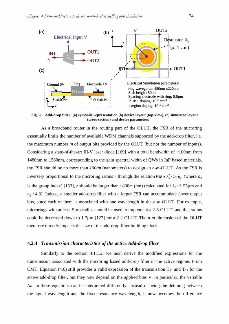
Chapter 4 From architecture to device: multi-level modelling and simulation 74
Electrical Input V
OUT2
OUT1IN1λi
λx P+
V
N+
IN1 OUT1
OUT2
Resonator λx
(x=1…m)
(a) (b)
y
x
z
x
(c)
ring waveguide: 450nm x220nmSlab height: 50nmSpacing electrode with ring: 0.6µmP+/N+ doping: 1019 cm-3
i-region doping: 1015 cm-3
Electrical Simulation parameters:
Si slab-P+
Ring Electrode +V
Si slab-N+
Ground 0V
Si-i type
Electrical Input V
OUT2
OUT1IN1λi
λx P+
V
N+
IN1 OUT1
OUT2
Resonator λx
(x=1…m)
(a) (b)
y
x
y
x
z
x
z
x
(c)
ring waveguide: 450nm x220nmSlab height: 50nmSpacing electrode with ring: 0.6µmP+/N+ doping: 1019 cm-3
i-region doping: 1015 cm-3
Electrical Simulation parameters:
Si slab-P+
Ring Electrode +V
Si slab-N+
Ground 0V
Si-i type
Fig.32. Add-drop filter: (a) symbolic representation (b) device layout (top-view), (c) simulated layout (cross-section) and device parameters
As a broadband router in the routing part of the OLUT, the FSR of the microring
essentially limits the number of available WDM channels supported by the add-drop filter, i.e.
the maximum number m of output bits provided by the OLUT (but not the number of inputs).
Considering a state-of-the-art III-V laser diode [169] with a total bandwidth of ~100nm from
1480nm to 1580nm, corresponding to the gain spectral width of QWs in InP based materials,
the FSR should be no more than 100/m (nanometers) to design an n-m-OLUT. As the FSR is
inversely proportional to the microring radius r through the relation gx rnFSR πλ 2/2≈ (where ng
is the group index) [153], r should be larger than ~800m (nm) (calculated for λx ~1.55µm and
ng ~4.3). Indeed, a smaller add-drop filter with a larger FSR can accommodate fewer output
bits, since each of them is associated with one wavelength in the n-m-OLUT. For example,
microrings with at least 5µm-radius should be used to implement a 2-6-OLUT, and this radius
could be decreased down to 1.7µm [127] for a 2-2-OLUT. The n-m dimension of the OLUT
therefore directly impacts the size of the add-drop filter building block.
4.2.4 Transmission characteristics of the active Add-drop filter
Similarly to the section 4.1.1.2, we next derive the modified expressions for the
transmission associated with the microring based add-drop filter in the active regime. From
CMT, Equation (4.6) still provides a valid expression of the transmission T11 and T21 for the
active add-drop filter, but they now depend on the applied bias V. In particular, the variable
∆λ in these equations can be interpreted differently: instead of being the detuning between
the signal wavelength and the fixed resonance wavelength, it now becomes the difference
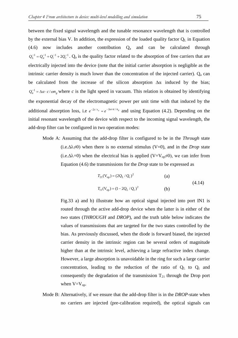
Chapter 4 From architecture to device: multi-level modelling and simulation 75
between the fixed signal wavelength and the tunable resonance wavelength that is controlled
by the external bias V. In addition, the expression of the loaded quality factor QL in Equation
(4.6) now includes another contribution Qa and can be calculated through 1111 2 −−−− ++= ciaL QQQQ . Qa is the quality factor related to the absorption of free carriers that are
electrically injected into the device (note that the initial carrier absorption is negligible as the
intrinsic carrier density is much lower than the concentration of the injected carrier). Qa can
be calculated from the increase of the silicon absorption ∆α induced by the bias;
ga ncQ ωα /1 ⋅∆=− where c is the light speed in vacuum. This relation is obtained by identifying
the exponential decay of the electromagnetic power per unit time with that induced by the
additional absorption loss, i.e ga ntct ee //2 ⋅∆−− = αt and using Equation (4.2). Depending on the
initial resonant wavelength of the device with respect to the incoming signal wavelength, the
add-drop filter can be configured in two operation modes:
Mode A: Assuming that the add-drop filter is configured to be in the Through state
(i.e.∆λ≠0) when there is no external stimulus (V=0), and in the Drop state
(i.e.∆λ=0) when the electrical bias is applied (V=Vop≠0), we can infer from
Equation (4.6) the transmissions for the Drop state to be expressed as
2op21 )/2()V( cL QQT =
2op11 )/21()V( cL QQT −=
(a) (4.14) (b)
Fig.33 a) and b) illustrate how an optical signal injected into port IN1 is
routed through the active add-drop device when the latter is in either of the
two states (THROUGH and DROP), and the truth table below indicates the
values of transmissions that are targeted for the two states controlled by the
bias. As previously discussed, when the diode is forward biased, the injected
carrier density in the intrinsic region can be several orders of magnitude
higher than at the intrinsic level, achieving a large refractive index change.
However, a large absorption is unavoidable in the ring for such a large carrier
concentration, leading to the reduction of the ratio of QL to Qc and
consequently the degradation of the transmission T21 through the Drop port
when V=Vop.
Mode B: Alternatively, if we ensure that the add-drop filter is in the DROP-state when
no carriers are injected (pre-calibration required), the optical signals can
Chapter 4 From architecture to device: multi-level modelling and simulation 76
propagate to the DROP port without getting additional carrier absorption loss
in the resonator. While the add-drop is switched into the THROUGH-state,
the carriers are filled into the intrinsic region of the ring resonator. However,
for this case, the input signal will be forwarded directly to the THROUGH
port, so that it does not get trapped nor does it experience any carrier
absorption in the cavity. It is therefore energetically advantageous to use
Mode B rather than Mode A. If we assume that the add-drop resonance is
configured to be initially aligned with the incoming signal wavelength λi (i.e.
∆λ=0) when there is no external bias (V=0), we
obtained 211 )/21()0( cL QQVT −== and 2
21 )/2()0( cL QQVT == . In this case, the
expression of QL is also different from that in Mode A since it excludes the
additional Qa that appeared for Mode A when V=Vop3. The column c) and d)
in Fig.33 shows the optical signal propagation and the corresponding truth
table for this configuration. Comparing with the values of T21 reached for
Mode A (see Fig.33 (b)), we see that the issue of transmission reduction by
carrier absorption in the ring is avoided in this configuration.
Following this comparison, the operation mode B is considered throughout Chapter 5
of the thesis. We also highlight that because the input signal wavelength is initially aligned
with the resonance (at V=0), the wavelength shift (∆λ) of Equation (4.6) is now directly equal
to the electrically induced wavelength shift of the resonance in this mode. Finally, a rather
hard constraint for this configuration is that it requires some pre-calibration scheme to make
sure that the initial resonance wavelength is aligned. As mentioned earlier, the micro-heater
approach relying on the thermo-optic effect could be adopted in this case.
a) Mode A (V=0) b) Mode A (V=Vop) c) Mode B (V=0) d) Mode B (V=Vop)
Signal propagati
on scenario
THROUGH
IN
V=0
OUT2
OUT1
IN2
THROUGH
IN
V=0
OUT2
OUT1
IN2
DROP
IN
V≠0OUT2
OUT1
IN2
DROP
IN
V≠0OUT2
OUT1
IN2
DROP
IN
V=0OUT2
OUT1
IN2
DROP
IN
V=0OUT2
OUT1
IN2
THROUGH
IN1
V≠0
OUT2
OUT1
IN2
THROUGH
IN1
V≠0
OUT2
OUT1
IN2 Targeted
Signal logic at OUT2
‘0’ ‘1’ ‘1’ ‘0’
3 if we assume the ring scattering loss is negligible (Qi significantly larger than Qc), it reduces to 11 2 −− = cL QQ , ideally resulting in the targeted values of transmission )0(21 =VT = 1 and )0(11 =VT = 0 for the DROP state.

Chapter 4 From architecture to device: multi-level modelling and simulation 77
T11 [ ] 1/2)/21(1
1 2
2
+∆
−−−
λλL
cL
QQQ 2)
//2//
(acic
acic
QQQQQQQQ
+++ 2)
/2/(
ic
ic
QQQQ
+
[ ] 1/2)/21(1
1 2
2
+∆
−−−
λλL
cL
QQQ
T21 [ ] 1/2
)/2(2
2
+∆ λλL
cL
QQQ
2)
//22(
acic QQQQ ++
2)/2
2(ic QQ+
[ ] 1/2
)/2(2
2
+∆ λλL
cL
QQQ
Spectrum
λ
λi
T21
λres λ
λi
T21
λres λ
T21
λres
λi
λ
T21
λres
λi
λ
λiT21
λres λ
λiT21
λres λ
λi
T21
λres λ
λi
T21
λres
Fig.33. Active add-drop filter operations in Mode A and Mode B when in the Through-state and Drop-state. Each scenario is associated with the targeted switch logic value at OUT2, the transmission
values at the Through and the Drop port, and the corresponding transmission spectrums at OUT2 highlighting the signal wavelength (red arrow) and the resonant wavelength of the add-drop filter.
4.2.5 Calculation of electrical control and power consumption
As discussed in section 4.2.2, the change of the free carrier concentration ∆N to be
reached in the electro-optic add-drop filter can be inferred from the required refractive index
change, or equivalently the resonance wavelength shift ∆λ needed to switch the ring state.
Then, the associated electrical bias conditions {V, I}, the serial resistance, as well as the
electrical power consumption, can be calculated using electrical simulation tools, such as
RSoft multiphysics [130]. It establishes the carrier and transport models for the silicon active
devices by applying the drift-diffusion system of equations (i.e. carrier continuity equations,
Poisson’s equation) onto the bulk semiconductor region. Typically, it creates a cross-section
of the device that is made of rectangular semiconductor elements and electrodes, for which
the material and doping conditions can be chosen. The geometry is then digitized with a non-
uniform (Delauney) mesh and the carrier transport equations are then solved via Gummel &
Newton-Raphson iteration [130]. The current density, the carrier concentration as well as
other electrical parameters for the given geometry are then obtained as a function of the
applied voltage.
For example, for a 4µm radius ring with a layout as shown in Fig.32, a current and
bias of {110µA, 0.92V} are required to achieve ∆N=2.65x1017 cm-3 and a shift ∆λ of 0.4nm at
λ =1.5µm. The static power consumption of the microring based add-drop is estimated from
Ps=VI (in Watts) and the dynamic switching energy consumed by the add-drop estimated as
VqCVE totsw 25.041 2 == (in Joules) [127, 133, 153] where qtot is the associated amount of
injected charges, C is the device capacitance and ¼ represents the assumed average
Chapter 4 From architecture to device: multi-level modelling and simulation 78
probability of performing the state transition (i.e. DROP to THROUGH) that needs carriers to
be injected [137].
4.2.6 Speed consideration for electro-refractive add-drop filters
The maximum data rate for such a SOI ring modulator without reverse bias is limited
to 1~2 Gbit/s, as given by the rise/fall time of the system response which can be directly
obtained by solving the classical transient equations of forward-biased PIN junctions (see
section 4.2.2). The section 4.2.2 also mentioned that the max{rise time, fall time} was
essentially limited by the free carrier lifetime for a standard SOI waveguide and could not be
reduced by using a simple higher direct {I, V} drive. Although there has been some
demonstration of silicon microring resonators operating at a speed >12.5Gbit/s with sub-
nanosecond switching time, they require the “pre-emphasis” scheme presented in section
4.2.2 where a higher forward biased electrical signal is used to reduce the carrier injection
time, as well as a high reverse bias voltage to quickly sweep out the free carriers. Such
requirements for a complex signal waveform at high-voltage operation however complicate
the design of low-energy CMOS driver circuits for the OLUT architecture. In fact, advanced
technology processes (28nm and 32nm) support 1V biased transistors. Moreover, the related
data rate increase is much slower than the increase of the total power consumption caused by
the higher electrical forward and reverse currents, such that the energy-per-bit figure of the
active add-drop filter could increase significantly. In addition, as mentioned previously (cf
section 4.2.1.3), reverse biased PN diode modulators can ideally run at a higher speed than
forward biased PIN diode modulator. However, the speed of these devices is practically
limited by the inductance of wire-bonding and the capacitance of the pn junction (e.g. a SOI
microring resonator based on carrier depletion with a data rate of ~3Gb/s under a reversed
bias of 5V was reported in [150]).
4.3 Multi-level modelling of OLUT and impact on the low level design of the OLUT building blocks
The design space is typically defined as the validity range of the device parameters
that allow the complex system built from these devices to reach a well identified set of
targeted system performances. Design space exploration is commonly referred to the activity
of discovering and evaluating design alternatives during system development for identifying
the best design tradeoffs. It is very useful for many engineering tasks, e.g. rapid prototyping,

Chapter 4 From architecture to device: multi-level modelling and simulation 79
optimization and system integration. Design space exploration is widely used by Electronic
design automation (EDA) tools to facilitate the design of complex computing systems
consisting of a large volume of building blocks, e.g. an IC integrated with billions of
individual transistors. Such a complex architecture is often described and optimized by using
various levels of design abstraction other than the register transfer level (RTL). This allows
designers to evaluate the impact of technology options not just at the device level, but also at
the architecture and application level, which can help designers to accelerate the technology
to architecture loop for generating the energy-efficient computing hardware evolved with
emerging applications. Similarly, the basic principle of this approach in EDA can be applied
to the design of our OLUT architecture.
The objective of this section is to provide the groundwork for design space exploration
of the proposed OLUT architecture. We first describe the multi-level modeling methodology
that efficiently generates and implements a functional and energy-efficient reconfigurable
computing architecture based on OLUTs. We then discuss the optical losses in the OLUT
architecture that will be used to evaluate the input laser power. A complete energy model for
the OLUT architecture will be presented in the last sub-section.
4.3.1 Overview of the multi-level modeling methodology
Fig.34 illustrates the design methodology. Ideally, for a given computing application
(e.g. ALU or full adder), our approach starts with architectural-level specifications (including
the number of OLUTs, the inputs and outputs dimensions of OLUTs, and the complementary
option) and then progressively goes down to the device level to design a functional OLUT.
Device level inputs include the size (ring radius), the Q factor and the wavelength shift of the
add-drop filters, which will be used to evaluate the key device characteristics by performing
physical simulation and modeling, e.g. FDTD, electrical simulations and CMT modeling. The
characteristics of other components in the functional toolbox using silicon photonics
technology (e.g. lasers and photodetectors as well as the waveguide losses) are fetched from
the library. Different input data and memory configurations (specified by the target
application) are considered to simulate the energy consumption of a single OLUT block. The
energy-efficient analysis is achieved under a given Bit Error Rate (BER) and the result is an
energy map giving the feasible design space of an OLUT, which is represented by the Q
factor and the wavelength shift of the add-drop filter. The optimal energy efficiency of an
OLUT is obtained by automated design space exploration of device parameters (e.g. Q factors

Chapter 4 From architecture to device: multi-level modelling and simulation 80
and the wavelength shift). Other OLUT metrics such as performance, latency or area usage
can also be evaluated as a function of the device parameters within the design space. After
that, we move again to the system level: we evaluate the performance and the energy
efficiency of the computing architecture according to various system-level design options
such as the number and the size of OLUTs and the interconnect topology (e.g. number of
waveguides and number of wavelengths) as well as the interface characteristics. However,
system-level design space exploration is currently a manual process. It indeed needs
automated back and forth between the results and the system-level specifications to
investigate the alternative architecture option that would provide the optimal results (e.g. best
energy efficiency) for the given test bench. Such a design exploration requires automated
tools for mapping application benchmarks (e.g. MCNC[117]), taking into account the main
advantage of OLUTs, i.e. the parallel computation on a same set of data. The implementation
of such tool is part of future works.
In the following, we present the optical loss model that links the constraint of the
system reliability (BER) and the device parameters.
Device level specification:r, ∆λ, Qc
System level specification:Number of OLUTs, n, m, complementary, etc.
Input data, configurationInput data,
configurationApplication (e. ALU, full
adder)
Application (e. ALU, full
adder)
PD, laser, waveguide losses, etc.
PD, laser, waveguide losses, etc.
Interconnect topology, interfaces
Interconnect topology, interfaces
Energy efficiency analysis
BER<10-18
Result:A functional and energy-efficient OLUT
Result:A functional and energy-efficient reconfigurable computing architecture
using silicon photonics technoloy
library libraryTest benchTest bench
Design Space Exploration
Design Space exploration
Fig.34. Illustration of a multi-level modeling methodology for designing a functional and energy-efficient
photonic reconfigurable computing architecture based on OLUTs
4.3.2 Optical losses in OLUT architectures
The computation performed by the electro-optic OLUTs relies on the optical signals
emitted from the light sources and that propagate across the OLUT building blocks. These
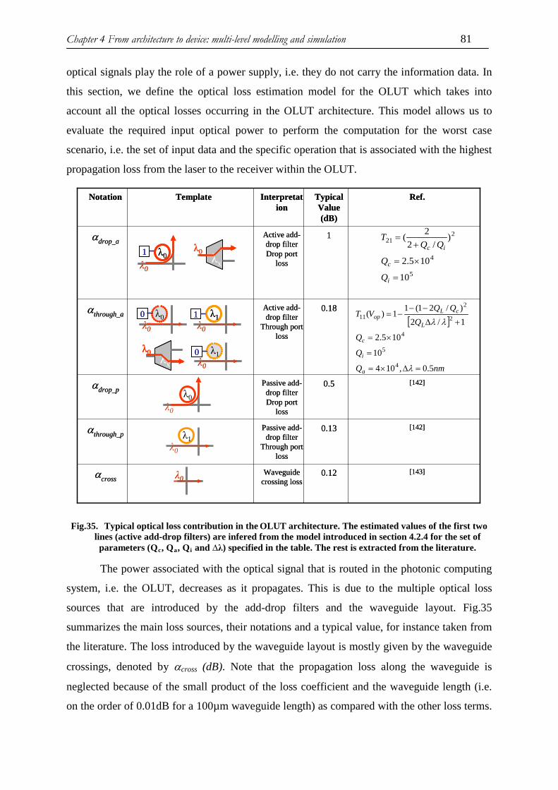
Chapter 4 From architecture to device: multi-level modelling and simulation 81
optical signals play the role of a power supply, i.e. they do not carry the information data. In
this section, we define the optical loss estimation model for the OLUT which takes into
account all the optical losses occurring in the OLUT architecture. This model allows us to
evaluate the required input optical power to perform the computation for the worst case
scenario, i.e. the set of input data and the specific operation that is associated with the highest
propagation loss from the laser to the receiver within the OLUT.
Template
αcross
αthrough_p
αdrop_p
αthrough_a
αdrop_a
Notation
[143]0.12 Waveguide crossing loss
[142]0.13 Passive add-drop filter
Through port loss
[142]0.5 Passive add-drop filter Drop port
loss
0.18 Active add-drop filter
Through port loss
1 Active add-drop filter Drop port
loss
Ref.Typical Value (dB)
Interpretation
λ0λ0
1 λ0λ0
11 λx
λ0λx
λ0
λ0 λ1λ0 λ0
λx
λ0 λ1λ0
0 1
0
λ0 λ1λ0 λ0
λx
λ0λx
λ0 λ1λ0
00 11
00
λ0λ0
5
4
221
10
105.2
)/2
2(
=
×=
+=
i
c
ic
Q
Q
QQT
[ ]
nmQ
Q
Q
QQQVT
a
i
c
L
cLop
5.0,104
10
105.2
1/2)/21(1
1)(
4
5
4
2
2
11
=∆×=
=
×=
+∆
−−−=
λ
λλ
λ0λ0
λ1λ0
Fig.35. Typical optical loss contribution in the OLUT architecture. The estimated values of the first two lines (active add-drop filters) are infered from the model introduced in section 4.2.4 for the set of parameters (Qc, Qa, Qi and ∆λ) specified in the table. The rest is extracted from the literature.
The power associated with the optical signal that is routed in the photonic computing
system, i.e. the OLUT, decreases as it propagates. This is due to the multiple optical loss
sources that are introduced by the add-drop filters and the waveguide layout. Fig.35
summarizes the main loss sources, their notations and a typical value, for instance taken from
the literature. The loss introduced by the waveguide layout is mostly given by the waveguide
crossings, denoted by αcross (dB). Note that the propagation loss along the waveguide is
neglected because of the small product of the loss coefficient and the waveguide length (i.e.
on the order of 0.01dB for a 100µm waveguide length) as compared with the other loss terms.

Chapter 4 From architecture to device: multi-level modelling and simulation 82
Regarding the add-drop filters, the transmission losses of the active add-drop filters that are
driven by carrier injection are computed from the associated Q factors according to the
relation (4.6), while that of the passive ones are taken from the literature to get more realistic
numbers associated with the state-of-the-art silicon photonics technology. These losses are
denoted as αdrop(dB), αthrough (dB) for the Drop and Through state respectively. The typical
loss value at the Drop port of the active add-drops is larger than that of the passive ones due to
the additional absorption loss caused by the electrically injected carriers for the active devices.
We thus use different terms to distinguish them: αdrop_a(dB), αthrough_a (dB) and αdrop_p(dB),
αthrough_p(dB) denote the losses occurring in the active and passive add-drop filters
respectively. The OLUT total loss is the sum (in dB) of the above-mentioned loss
contributions along the signal path. It essentially depends on the OLUT system dimensions,
e.g. the number of inputs n, the number of outputs m, and the physical parameters of the
OLUT building blocks such as the ring geometry, the quality factor of the micro-resonator
based add-drop filter and the spectral-shift ∆λ chosen for driving the add-drop filters of the
OLUT. From comparing the different values listed in Fig.35, we can infer that the total optical
power loss of the n-m-OLUT will be predominantly governed by the contribution of the active
add-drop filters (as well as the passive ones in the Drop state for the n-mx2-OLUTs). The loss
term αdrop_a and αthrough_a are indeed the greatest contributions to the total optical power loss
of the n-m-OLUT.
For simplification, the Through-port transmission losses of the active add-drop filters
in the memorization part are considered to be identical for all the incoming wavelengths that
are out of resonance with the add-drop filter4. The total loss of n-m-OLUTs therefore linearly
increases with the number of the memorization stages, i.e. with the number m of output bits.
For the particular case of the n-mx2-OLUTs, the evaluation of the worst-case optical power of
the n-mx2-OLUTs includes all the contributions listed in the Fig. 35, since some additional
components such as the passive add-drop filters (the number of which increases with the
number m of output bits) are specifically needed by this architecture. According to the values
4 We assume here that for the jth column of the memorization stage, the transmission T11(λk) of the active add-drop filter at the signal wavelength λk is equal to αthrough_a for all k≠j. This seems to be a rather conservative assumption, as the associated wavelength shift in this case is likely to be larger than that needed to drive the add-drop filter from the Drop to the Through state for the λj wavelength of interest of the jth column of the memorization stage
Chapter 4 From architecture to device: multi-level modelling and simulation 83
listed in the above table though, a reasonable input optical power overhead is expected for the
n-mx2-OLUT as compared to the n-m-OLUT5.
Finally, we reemphasize here that the loss values of the active add-drop filter that are
given in Fig.35 are just example values derived from Equation 4.6 for a chosen set of device
parameters (Qc, Qi and ∆λ). In practice, the worst-case optical path might be different for each
set of device parameters. It is evaluated in each case by comparing the total loss for all optical
paths followed upon varying the input data and the computed Boolean function. Based on this
loss model, the energy dissipation from the lasers to the detectors, i.e. basically the minimum
amount of optical power delivered by the laser sources for driving the OLUTs is obtained. In
the next sub-section, we present the energy model for the electro-optic implementation of the
OLUT architecture, including all the various contributions from the lasers, the add-drop filters
and the photodetectors.
4.3.3 OLUT energy model
The overall OLUT energy consumption is driven by the static and dynamic energies
required by each switching element (denoted by Ed and Es), as well as the energy required by
the laser sources (Elaser) and photodetectors (Epd) to transmit and detect the optical signals.
Therefore the overall dissipated energy-per-output-bit for an n-m-OLUT can be estimated as
pdlasersdOLUT EEEEE +++= (4.15)
It depends on the OLUT system dimensions (i.e. number of output bits m, and input
bits n) and on the device characteristics. Fig.36 reminds the general architecture of n-m-
OLUTs with n data inputs and m data outputs highlighting the related number of active add-
drop filters, as well as the number of photodetectors (i.e. one “active” per output bit6) and
lasers (one per input bit) in n-m-OLUTs. The general architecture of the n-mx2-OLUT is also
recalled on Fig.36(b), which highlights that the main difference is related to the m passive
add-drop filters and the m additional photodetectors in the complementary part. Note that the
passive add-drop filters do not consume any energy as such but they will indirectly contribute
to the energy consumption of the computing architecture through increasing the required Elaser
5 The detailed comparison of input optical power and energy dissipation between n-mx2-OLUTs and n-m-OLUTs can be found in section 5.2 6 Given the refined layout of Fig 26, the n-m-OLUT has 2n photodetectors per output bit, but only one is active and consumes energy at any time.

Chapter 4 From architecture to device: multi-level modelling and simulation 84
upon adding some optical losses along the optical paths of the n-mx2-OLUT. We discuss the
contribution of the total energy for the n-m-OLUT in detail in the next section.
n
2n
Routing partMemorization part
…
……
…
0/1
m
… …
m lasers … m stages …
…
…
… …
0/1
0/1
0/1
nB: input data rate mB: output data rate
B: data rate (bit/s)
2n-1 add-drop filters
add-drop filters
- Dynamical energy: Ed- Static energy: Es
- Static energy: Es
- Elaser
- Epd
m photodetectors
2n
n
2n
Routing partMemorization part
…
……
…
0/10/1
m
… …
m lasers … m stages …
…
…
… …
0/10/1
0/10/1
0/10/1
nB: input data rate mB: output data rate
B: data rate (bit/s)
2n-1 add-drop filters
add-drop filters
- Dynamical energy: Ed- Static energy: Es
- Static energy: Es
- Elaser
- Epd
m photodetectors
2n
n
2n
Routing part
Memorization part
…
……
…
0/1
m
… …
m lasers … m stages …
…
…
… …
0/1
0/1
0/1
nB: input data rate
B: data rate (bit/s)
2n-1 active add-drop filters
Active add-drop filters
- Dynamical energy: Ed /2 - Static energy: Es /2 - Static energy: Es /2
- Elaser
- Epd
m photodetectors
2n
/omplementary part
……
m
…
… m stages …
…
…
…
2mB: output data rate
Passive add-drop filters
- Epd
m photodetectors
2n
…
n
2n
Routing part
Memorization part
…
……
…
0/10/1
m
… …
m lasers … m stages …
…
…
… …
0/10/1
0/10/1
0/10/1
nB: input data rate
B: data rate (bit/s)
2n-1 active add-drop filters
Active add-drop filters
- Dynamical energy: Ed /2 - Static energy: Es /2 - Static energy: Es /2
- Elaser
- Epd
m photodetectors
2n
/omplementary part
……
m
…
… m stages …
…
…
…
2mB: output data rate
Passive add-drop filters
- Epd
m photodetectors
2n
…
Fig.36. Reminders of (a) the general architecture of n-m-OLUTs associated with all the terms of energy dissipations (b) the general architecture of n-mx2-OLUTs associated with all the terms of energy
dissipations
4.3.3.1 Dynamic Energy Ed
The OLUT dynamic energy dissipation Ed (energy-per-output-bit, in J/bit) relies on the
switching activity of the 2n-1 add-drop filters in the routing part and is given by
Ed= (2n-1)× Esw/m (4.16)
Chapter 4 From architecture to device: multi-level modelling and simulation 85
where Esw was defined previously as the dynamic switching energy of one add-drop filter.
Since we assume an already configured OLUT and the state of the memorization part does not
change during the computation, no dynamic power is considered in this part of the OLUT.
4.3.3.2 Static Energy Es
The static energy Es (energy-per-output-bit, in J/bit) is estimated from the static electrical
power consumption of the add-drop filters in both the routing and the memorization part to
control the bias. Assuming that half of the add-drop filters are not switched by the input data
in the routing part, and that half of the add-drop filters in the memorization part are
configured to be in the DROP state (i.e. they are powered off), the static energy is given by
Es= 0.5×(2n-1+m×2n)×Ps/mB (4.17)
where B is the data rate per channel (in bit/s) (i.e. nB is the total input data rate and mB the
total output data rate of the OLUT), and Ps was defined previously as the static power
associated with the add-drop filter. The remaining factor stands for the total number of add-
drop filters in the n-m-OLUT. We use the same resonance wavelength shift ∆λ to change the
state of the add-drops in the estimation of Ed and Es. This implicitly assumes that the add-
drops that are dynamically switched in the routing part can almost reach the steady-state
(>95%) carrier concentration within the bit duration. This is a reasonable approximation when
the maximum data rate of the OLUT is less than ~1Gbit/s and considering that the free carrier
lifetime in SOI waveguide can be as short as ~450ps. We also consider the same power and
∆λ to drive the rings in all parts (memorization and routing) of the OLUT, since the associated
diameters are approximately identical. Finally, it is worth reminding that for a practical
implementation of the OLUT using the mode B configuration of the add-drop filters, a pre-
calibration scheme would be required which we do not include in our evaluation of the OLUT
power consumption, as derived in Chapter 5. We only observe here that the static energy
would thus also depend on the initial spectral mismatch between the signal and the add-drop
resonance caused by the fabrication uncertainty. In principle, this deviation could be corrected
by a thermo-optic tuning scheme, as following: considering an inaccuracy of 5nm when
fabricating a 7µm microring (∆r=10nm), it would approximately cause a wavelength shift of 1
nm (at 1.55µm)7. This could be compensated by heating the add-drop filters by ~10°C (given
7 By assuming approximately λλ // ∆=∆ rr

Chapter 4 From architecture to device: multi-level modelling and simulation 86
that ∆λ/Τ=0.1nm/°C), thereby adding ~1pJ/bit to each add-drop filter that operates at the
speed of 1Gbit/s (assuming the heating efficiency is 0.1mW/°C [160,13]).
4.3.3.3 Energy dissipated by the photodetectors Epd
The energy consumed by the transmitter and receiver is estimated by using a back-
propagation method.
At the first step, given the bit error rate (BER) specification and the characteristics of
the photodiode, we need to evaluate the minimum difference of the input optical power (∆Precv)
required by the photodetector to distinguish logic ‘1’ and logic ‘0’ for maintaining the given
BER value. According to [135], considering that the BER is determined by the noise and the
difference between signal values that represent logic ‘1’ and logic ‘0’ in a binary signaling
system, ∆Precv is calculated from the BER as:
ℜ=∆ − /))2(( 212 BERerfciP Nrecv (4.18)
where R (in A/W) represents the responsivity of the integrated photodetector, 2Ni is the
photodetector internal noise in terms of average root-mean squared, efrc-1 is the inversed error
function and efrc-1(2BER)2 is the system signal-to-noise ratio (SNR) that is required to get a
given BER. For example, considering a state-of-the-art Si/Ge integrated PIN photodetector
with a quantum efficiency of ~1.08A/W and a dark current around zero-bias of 0.1µA [125],
∆Precv is ~3.8µW for ensuring a bit-error-rate (BER) of 10-18. This power can be translated
into ~4fJ photon energy per bit given a 1Gbit/s data rate, which generates a charge of a few fC
given the quantum efficiency. If we assume the photodiode has a capacitance of several fF
[13], the energy consumption of the photodetector Epd is approximately 10fJ/bit independently
the number of output bits (one photodetector corresponds to one output port).
4.3.3.4 Energy dissipated by the laser Elaser
Then, knowing ∆Precv for the OLUT circuit layout and the optical losses in its different
parts, we can calculate the minimum required output optical power at the source Plaser. This
power is associated with the laser energy consumption (fJ/bit) through
BPVE laserddLaser /)/( η= (4.19)

Chapter 4 From architecture to device: multi-level modelling and simulation 87
where Vdd is the supply voltage and η (W/A) is the laser differential efficiency. Since
we consider lasers as a global power supply for reconfigurable photonic systems based on
many OLUTs, the static electrical power consumption is not included for the evaluation of
Elaser within a single OLUT8.
Since optical signals (representing the logic levels) are affected by the total
transmission loss and this loss can vary for different optical paths in a photonic system as
OLUT, a simple threshold cannot reliably distinguish between ‘0’ and ‘1’ for OLUTs. To
solve this problem, Plaser is calculated by using differential signaling, as follows: we evaluate
the “worst-case” optical path that exhibits the maximum optical loss from the laser to the
photodetector. It corresponds to the minimum signal transmission among all scenarios where
the desired output is logic “1”, denoted by 1min. Similarly, to avoid the logic determination
failure in the photodetector, we take into account the maximum leakage transmissions of all
the signals arising from the undesired ports and accumulated into the receiver where logic ‘0’
is expected, denoted by 0max. Both transmissions values 1min and 0max (in absolute, no unit)
depend on the input logic values and on the memory configurations of the OLUT. Finally, we
use the difference between 1min and 0max to evaluate Plaser through
)01/( maxmin −∆= recvLaser PP (4.20)
It is worth noting that this condition is extremely conservative, as it uses the minimum
difference in two different powers representing the logic level among all the optical paths, and
distinct optical paths of the OLUT are likely to be associated with either a higher value than
1min or a lower value than 0max.We present as an example, in a 2-1-OLUT, the various
possible cases corresponding to 1min and 0max in Fig.37 (a) and (b), respectively.
8 It is worth noting that the obtained Elaser for an OLUT block is underestimated in the current model. The static power consumption of the laser sources needs to be included if this model is used for a reconfigurable system integrated with a large number of OLUTs.

Chapter 4 From architecture to device: multi-level modelling and simulation 88
D
1
λ0
λ0
λ0λ0
D
λ0
λ0
λ0 1λ0
a) 1min=min{ 1A,1B,1C,1D }
D
λ0
λ0
λ0
1λ0
D
λ0
λ0
λ0
1
λ0
1B 1C 1D1A
0B 0C 0D
b) 0max=max{ 0A,0B,0C,0D }
0AD
0
λ0
λ0
λ0 111
1 1 1 0 0 1 0 0
1 1 1 0 0 1 0 0
000
00
00
000
0
0
D
1
λ0
λ0
λ0 011
D
1
λ0
λ0
λ0 101
D
1
λ0
λ0
λ0 110
D
11
λ0
λ0
λ0λ0λ0λ0
D
λ0
λ0
λ0 111λ0
a) 1min=min{ 1A,1B,1C,1D }
D
λ0
λ0
λ0
111λ0
D
λ0
λ0
λ0
111
λ0
1B 1C 1D1A
0B 0C 0D
b) 0max=max{ 0A,0B,0C,0D }
0AD
0
λ0
λ0
λ0 111
D
00
λ0
λ0
λ0 111111111
1 1 1 0 0 1 0 0
1 1 1 0 0 1 0 0
000000000
000000
000000
000000000
000
000
D
1
λ0
λ0
λ0 011
D
11
λ0
λ0
λ0 000111111
D
1
λ0
λ0
λ0 101
D
11
λ0
λ0
λ0 111000111
D
1
λ0
λ0
λ0 110
D
11
λ0
λ0
λ0 111111000
Fig.37. Evaluation of the worst-case scenario to estimate the value of 1min and 0max (continuous lines represent signal propagation, dashed lines represent the routing and accumulation of leakage power)
In the case where all optical loss values are fixed, it seems simple to conclude on the
worst case scenario in the general case. However, as we change the design parameters of n-m-
OLUTs (such as the number of inputs, the number of outputs, the Q factor of the add-drop
filter, and the wavelength shift to drive them), the worst case scenario used to estimate Plaser
may be different for each set of parameters (i.e. when accounting for the actual transmission
values derived from the model of the active add-drop filters).
In addition, it should be pointed out that the energy model introduced here is not only
valid for n-m-OLUTs, but also for n-mx2-OLUTs upon making two modifications to the model.
First, 2m now is the number of output bits and it should be used accordingly in the equations
that give the different energy contributions. Secondly, Elaser should be computed from the
worst-case scenario that includes all the loss terms listed in Fig.35, taking into account the
additional number of output stages in the complementary part. We note that since the number
of photodetectors is doubled like the number of output bits, this energy contribution remains
similar to that of the n-m-OLUT though.
4.4 Conclusions
In this chapter, we proposed a physical implementation of the photonic components
required for building the OLUT architecture. We focused on using the electrically-controlled
silicon microring resonators as the active add-drop filters that are the essential active devices
of the OLUT presented in Chapter 3 . We showed how to design and model these components

Chapter 4 From architecture to device: multi-level modelling and simulation 89
for a system level estimation of the performance for the resulting OLUT. We are aware that
the landscape of silicon photonics is moving extremely fast with new integrated devices
reported every year. However, our modeling work does not rely on new breakthroughs in
device performance, i.e. speed, power or efficiency. Instead we focus on investigating how
some mature silicon photonic devices (hereby silicon microring based add-drop filters) should
be designed for the OLUT computing architecture to reach system-level performance
requirements. In this context, we have proposed, in the last section of the chapter, a multi-
level modeling methodology based on the design space exploration at the device level for
estimating the system performance. This method therefore aims to study the feasibility of the
OLUT architecture. In the following chapter, we will estimate and discuss the associated
performance of the resulting OLUT using the energy model and the physical implementation
proposed here and comparing the different OLUT architectures that have been introduced.

Chapter 4 From architecture to device: multi-level modelling and simulation 90
Chapter 5 Performance evaluation of the electro-optic OLUT implementation 91
Chapter 5 PERFORMANCE EVALUATION OF THE ELECTRO-OPTIC OLUT IMPLEMENTATION
In this chapter, we perform the design space exploration for the electro-optic OLUT
architecture using the multi-level modeling approach based on the device physical
implementation and the energy model developed in Chapter 4. The chapter is organized as
follows. In section 5.1, we start with a basic 2-2-OLUT example for which we first define the
feasible design space related to the parameters of the underlying add-drop filters. We then
analyze the relation between the estimated OLUT system energy dissipation and the key
technological parameters of the devices when the number of output bits increases from 2 up to
8. We show the key advantage of n-m-OLUTs for performing energy-efficient logic
computation through the example of a 1-bit Arithmetic Logic Unit (ALU). In addition, the
impact of the OLUT input dimension on the device parameters and in turn on the system
energy efficiency is studied. In section 5.2, we present the evaluation results for the n-mx2-
OLUT architecture. By comparing the n-m×2-OLUT architecture with that of n-m-OLUTs
through the implementation of a 1-bit ALU, the benefits in terms of energy and hardware
efficiencies for the n-m×2-OLUT architecture are highlighted. We conclude this chapter in
section 5.3.
5.1 Case study and result analysis for n-m-OLUTs
5.1.1 A review of the energy model introduced in chapter 4
Before discussing the results for the performance evaluation obtained from the energy
model, we review its basic principles and re-clarify the relation between the parameters
describing the add-drop filters and the energy consumption for the OLUT based on an electro-
optic implementation. The equations and the constant values used by the model are listed in
Fig.38. We remind here that the overall OLUT energy consumption EOLUT (i.e. energy-per-
output-bit, given by Equation (a) in the figure) is the sum of the following contributions:
i) Ed (cf. Equation (4.17)) represents the dynamic energy dissipated by the add-drop
filters for performing the state transition (Drop to Through) that needs carriers to be
injected to tune the resonant wavelength;
Chapter 5 Performance evaluation of the electro-optic OLUT implementation 92
ii) Es (cf. Equation (4.18)) is the static energy consumed by the add-drop filters and is
determined by the electrical bias and current obtained from the electrical simulation of
PIN based silicon microring resonator;
iii) Elaser (cf. Equation (4.19)) is the minimum input optical power delivered by the
laser to distinguish the logic ‘1’ with logic ‘0’(according to the laser energy
dissipation within the OLUT) for reaching an acceptable bit error rate (BER=10-18 is
chosen here, i.e. considering error free is reached for one error per 1018 data bits);
iv) Epd is an estimation of the energy dissipated by each photodetector and is set to be
10fJ/bit at the frequency of 1GHz.
As mentioned previously (cf Equation (4.6)), the parameters for fully describing the
operation of the add-drop filters are the coupling quality factor Qc, the wavelength shift
∆λ between the resonance and the incoming signal wavelength as well as the intrinsic quality
factor Qi. Since Qi is generally fixed by a given technology and for a given technology by the
ring radius (as shown in Fig.35(c) in section 4.1), the transmissions of the add-drop filter in
the active regime are thus expressed according to the values of Qc and ∆λ, thereby we build
the feasible design space based on the values of the coupling quality factor Qc as well as the
wavelength shift ∆λ. For a given number of input and output bits n and m:
• Higher Ed and Es are required for operating the n-m-OLUT with an increasing
wavelength shift ∆λ, since more carriers are required to be injected. But Ed and Es are
both independent of Qc.
• However, Elaser is inversely proportional to the minimum difference between the
worst-case transmission values for logic ‘1’ and logic ‘0’ (1min and 0max in equation (b)
in Fig.38) and thus relies on the Qc and the ∆λ. On the one hand, for a larger
wavelength shift ∆λ, an increased transmission value is generally obtained at the
Through port when the add-drop filter is in the Through-state, thereby facilitating the
distinction of logic ‘1’ and logic ‘0’, which in turn should lead to a smaller Elaser to be
used for driving the OLUT 9 . On the other hand, as shown by the transmission
expressions in Fig.38, for an increased value of Qc (or more precisely of the ratio
Qc/Qi), it is more difficult to achieve the Drop-state when the add-drop filter is
9 In fact, Qa also decreases with ∆λ increasing (which is taken into account in our model), but the negative impact on T11 through a decrease of QL is in fact overcompensated by the increase of ∆λ.
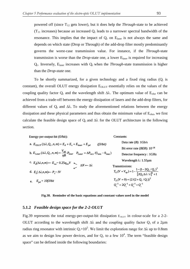
Chapter 5 Performance evaluation of the electro-optic OLUT implementation 93
powered off (since T12 gets lower), but it does help the Through-state to be achieved
(T11 increases) because an increased Qc leads to a narrower spectral bandwidth of the
resonance. This implies that the impact of Qc on Elaser is not always the same and
depends on which state (Drop or Through) of the add-drop filter mostly predominantly
governs the worst-case transmission value. For instance, if the Through-state
transmission is worse than the Drop-state one, a lower Elaser is required for increasing
Qc. Inversely, Elaser increases with Qc when the Through-state transmission is higher
than the Drop-state one.
To be shortly summarized, for a given technology and a fixed ring radius (Qi is
constant), the overall OLUT energy dissipation EOLUT essentially relies on the values of the
coupling quality factor Qc and the wavelength shift ∆λ. The optimum value of Eolut can be
achieved from a trade-off between the energy dissipation of lasers and the add-drop filters, for
different values of Qc and ∆λ. To study the aforementioned relations between the energy
dissipation and these physical parameters and thus obtain the minimum value of Eolut, we first
calculate the feasible design space of Qc and ∆λ for the OLUT architecture in the following
section.
pdlasersdcOLUT EEEEmnQE +++=∆ ),,,( λ
laserdd
cLaser PB
VmnQEη
λ =∆ ),,,(
a.
b. )01/( maxmin −∆= recvLaser PP
c. Vqtot25.0Ed(∆λ,n,m)← Esw~
Es( ∆λ,n,m)← Ps~ IV
∆N ← ∆λ←←
d.
Constants:Energy-per-output-bit (fJ/bit):
Data rate (B): 1Gb/s
Bit error rate (BER): 10-18
Epd = 10fJ/bite.
(fJ/bit)
Wavelength λ: 1.55µm
Detector frequency : 1GHz
[ ]
1111
221
2
2
11
2
))/2/(2()0(
1/2)/21(1
1)(
−−−− ++=
+==
+∆
−−−==
iacLQQQQ
QQVT
QQQVVT
ic
L
cLop
λλ
Transmissions:
Fig.38. Reminder of the basic equations and constant values used in the model
5.1.2 Feasible design space for the 2-2-OLUT
Fig.39 represents the total energy-per-output-bit dissipation EOLUT in colour-scale for a 2-2-
OLUT according to the wavelength shift ∆λ and the coupling quality factor Qc of a 2µm
radius ring resonator with intrinsic Qi=105. We limit the exploration range for ∆λ up to 0.8nm
as we aim to design low power devices, and for Qc to a few 104. The term “feasible design
space” can be defined inside the following boundaries:

Chapter 5 Performance evaluation of the electro-optic OLUT implementation 94
- For small values of Qc, the resonance linewidth is too broad, such that the wavelength
shift ∆λ must exceed the boundary value (e.g. ∆λ>0.8nm for Qc=3000) in order to
switch the add-drop filters to pass from the DROP to the THROUGH state with
sufficient extinction ratio.
- For large values of Qc, the ratio of Qc to the intrinsic Qi becomes too large, inhibiting
the resonant interference process in the resonators, and the DROP state cannot be
achieved anymore (e.g. if Qc/ Qi >0.5).
As shown in Fig.39, at the boundary of the feasible design space, the OLUT energy
dissipation is roughly two orders of magnitude higher than the minimum within the
feasible design space. This is due to the fact that the difference between the worst-case
transmission values of logic ‘1’ and logic ‘0’ (i.e. 1min - 0max) is too small, such that Elaser
has to increase significantly for guarantying the required bit error rate (see Equation (b) in
Fig.38).
0 1 2 3 4 5 6x 10⁴
0
0.1
0.2
0.3
0.4
0.5
0.6
0.7
0.8
1
1.5
2
2.5
3
3.5
4Log10(Energy [fJ/bit])
∆λ(n
m)
Qc
Min {Energy}=72 fJ/bit
Feasible Design Space
1
0 1 2 3 4 5 6x 10⁴
0
0.1
0.2
0.3
0.4
0.5
0.6
0.7
0.8
1
1.5
2
2.5
3
3.5
4Log10(Energy [fJ/bit])
∆λ(n
m)
Qc
Min {Energy}=72 fJ/bit
Feasible Design Space
1
Fig.39. Total energy dissipation (in fJ/bit) in 2-2-OLUTs according to ∆λ and Qc for ring radius of a) r =2µm (Qi~100,000). Invalid regions are represented by the white colour background

Chapter 5 Performance evaluation of the electro-optic OLUT implementation 95
0.1 0.2 0.3 0.4 0.5
50
100
150
200
EdEsELaserEpd
Rat
io (%
)
∆λ (nm)
(b)
0.1 0.2 0.3 0.4 0.50
50
100
150
Qc=30,000Qc=20,000Qc=10,000
Ener
gy (f
J/bi
t)(a)
E las
er(fJ
/bit)
(d)
∆λ (nm)0.1 0.2 0.3 0.4 0.50
100
200
300
400
500
Qc=30,000Qc=20,000Qc=10,000
E olu
t(fJ
/bit)
(c)∆λ (nm)
∆λ (nm)
0.1 0.2 0.3 0.4 0.50
20
40
60
80
100
EdEsELaserEpd
Fig.40. For a 2-2-OLUT (ring radius =2µm), (a) the energy dissipation (fJ/bit) across various components and (b) the ratio of these energy contributions relative to the total energy dissipation vs.
wavelength shift for Qc= 2x10⁴ (c) total energy dissipation (fJ/bit) and (d) laser energy dissipation Elaser vs. wavelength shift for Qc= 1x10⁴, 2x10⁴ , 3x10⁴
Within the remaining feasible design space in Fig.39, i.e. between these boundaries,
the minimum value of Eolut (72fJ/bit, see the marker #1 in Fig.39) is obtained for Qc~20,000
and ∆λ~0.2nm for a bias of {I,V} ={10µA, 0.87V} (i.e. computed from the electrical
simulation of a PIN junction based microring as discussed in section 4.2). This value results
from the trade-off between the energy dissipated by the add-drop filters and that of the lasers.
Indeed, as shown in Fig.40 (a) and (b) (which plot the energy consumed by each device class
and their associated ratios to the total energy Eolut in the 2-2-OLUT as a function of ∆λ for
Qc=20,000), the two main contributions to Eolut are the laser energy dissipation Elaser and the
static energy dissipated within the add-drop filters Es. For a fixed Qc, since the two
contributions Elaser and Es vary differently with ∆λ, a trade-off exists for minimizing Eolut. For
example, for ∆λ below ~0.2nm and above the minimum wavelength shift that can be used to
drive the add-drop filters (i.e. ∆λ =0.14nm), Eolut is globally reduced for increasing ∆λ due to

Chapter 5 Performance evaluation of the electro-optic OLUT implementation 96
the associated reduction of Elaser, which dominates the OLUT energy consumption Eolut.
Outside of this region, Eolut generally increases with ∆λ, since the ratio of Elaser to Eolut
decreases (from 80% down to 10% when ∆λ increases) and its reduction with increasing ∆λ is
overcompensated by the increase of the energy dissipated within the add-drop filters Es (that
increases from ~7% of Eolut for ∆λ of 0.15nm up to ~80% of Eolut when ∆λ is close to 0.5nm),
which ends up being the dominant contribution above ∆λ = 0.23nm. When the Es contribution
mostly determines the overall energy dissipation of the OLUT, Eolut becomes almost
independent of Qc at a fixed value of ∆λ, which is observed on the 2D energy map of Fig.39
above ∆λ of 0.4nm. It happens that the minimum energy dissipation is obtained when the ratio
of Epd reaches its maximum (Epd is fixed at 10fJ/bit, as presented previously).
Fig.40 (c) is a zoom in of Fig.39 and it shows the total energy dissipation of 2-2-
OLUTs (r=2µm) Eolut for ∆λ limited up to 0.5nm and for different values of Qc=1x10⁴, 2x10⁴
and 3x10⁴. While for the largest Qc, a smaller wavelength shift can be afforded to drive the
OLUT, the associated Eolut is not the minimum. As mentioned above, this is because at low
values of ∆λ, Elaser dominates over the energy dissipations within the add-drop filters, such
that the optimal Eolut is obtained when Elaser is closed to its minimum (by taken into account
the other contributions). Fig.40 (d) shows the energy consumed by Elaser in this 2-2-OLUT
(r=2µm) according to the ∆λ for Qc=1x10⁴, 2x10⁴ and 3x10⁴. It highlights that the impact of
Qc on Elaser is not always the same, which indeed depends on which state (Through or Drop)
of the add-drop filter predominantly governs the worst-case transmission value.

Chapter 5 Performance evaluation of the electro-optic OLUT implementation 97
0 1 2 3 4 5 6x 10⁴
0
0.1
0.2
0.3
0.4
0.5
0.6
0.7
0.8
1
1.5
2
2.5
3
3.5
4Log10(Energy [fJ/bit])
∆λ(n
m)
Qc
Min {Energy}=48 fJ/bit
Feasible Design Space
2
0 1 2 3 4 5 6x 10⁴
0
0.1
0.2
0.3
0.4
0.5
0.6
0.7
0.8
1
1.5
2
2.5
3
3.5
4Log10(Energy [fJ/bit])
∆λ(n
m)
Qc
Min {Energy}=48 fJ/bit
Feasible Design Space
2
Fig.41. Total energy dissipation (in fJ/bit) in 2-2-OLUTs according to ∆λ and Qc for add-drop filters based on microrings with a radius of r =7µm (Qi~500,000). Invalid regions are represented by the white colour background
The minimum shift that can be used to drive the OLUT is determined by the ratio of
Qc to Qi, i.e. intrinsically by Qi for a given range of Qc. According to [138] and as already
mentioned in section 4.1 of Chapter 4, Qi strongly depends on the radius of the ring for a
given technology process, thus leading to different feasible design spaces for different ring
sizes. Fig.41 presents the feasible design space associated with a larger Qi (~500,000) in a
7µm radius ring. We see that the design space is extended to values of Qc above 6x10⁴, where
Qc remains small compared to Qi ~5x10⁵, and a lower minimum value of the wavelength shift
of ~0.07nm can be used to drive the OLUT. The minimum wavelength shift therefore depends
on Qi and consequently on the device geometry, i.e. the ring radius. Intuitively, since a higher
Qc value results in a spectrally narrower (more selective) add-drop transfer function, a smaller
wavelength shift becomes sufficient for reaching a targeted signal-to-noise ratio (or bit error
rate). In Fig.41 a lower minimum of the energy-per-output-bit figure of 48fJ/bit (marker #2 in
Fig.41) is obtained for ∆λ=0.1nm when Qc is ~43,000. This is achieved with a reduced ratio
of Qc to Qi as compared to the small ring case (see Table 3), which ensures a larger DROP
state transmission of the add-drop filters, thereby leading to a reduced Elaser as compared with
the 2-2-OLUT (r=2µm). However, although the minimum injected carrier concentration

Chapter 5 Performance evaluation of the electro-optic OLUT implementation 98
decreases for the smaller optimal wavelength shift that can be afforded for the larger ring
case, it does not help reducing the total energy dissipation. This is because the reduction of
carrier concentration is compensated by the increased ring surface (that leads to an increased
amount of total charges within the device). Therefore, an optimum value likely exists for the
radius of the ring to minimize the total energy consumption. Given a range of the ring radius
from 2µm to 10µm, a minimum value for Eolut of 43fJ/bit is indeed obtained for r=5µm
(Qi~4x10⁵) for the 2-2-OLUT architecture. The minimum values of the total energy
dissipation and the associated parameters of the add-drop filters in 2-2-OLUT for r=2µm,
5µm and 7µm are summarized in the Table 3.
Tab 3. Minimum energy dissipation Eolut associated with specific values of the Q factors and the wavelength shift for 2-2-OLUTs with r=2µm, 5µm and 7µm microrings.
2-2-OLUT Qi min Eolut ∆λ Qc Qc /Qi
r=2µm 105 74 fJ/bit 0.2nm 20,000 0.2
r=5µm 4x10⁵ 43 fJ/bit 0.1nm 44,000 0.11
r=7µm 5x10⁵ 48fJ/bit 0.1nm 43,000 0.086
Fig.42 illustrates the ratio of energy dissipation in the different parts of the OLUT with
respect to the total energy dissipation in a 2-2-OLUT (2µm) according to the wavelength shift
∆λ when Qc is 2x10⁴. We can see that when ∆λ is around 0.2nm (corresponds to the minimum
value of Eolut), the energy dissipated in the different parts of the OLUT have a roughly similar
contribution to Eolut. In particular, the energy dissipated by the routing part accounts for a
relatively constant ratio i.e. ~30%. Since the routing part is shared by all the signals and it
does not scale with the wavelengths used, this part of energy dissipation can be reduced by
using more output bits for the OLUT architecture. In the following, we will investigate the
scalability of the n-m-OLUT architectures in terms of energy consumption and demonstrate
the benefits in energy efficiency upon increasing the number of output bits from 2 to 8.

Chapter 5 Performance evaluation of the electro-optic OLUT implementation 99
0.1 0.2 0.3 0.4 0.50
10
20
30
40
50
60
Rat
io (%
)
∆λ (nm)
Routing part
Memorization part
Laser
Photodetector
0.1 0.2 0.3 0.4 0.50
10
20
30
40
50
60
Rat
io (%
)
∆λ (nm)
Routing part
Memorization part
Laser
Photodetector
Fig.42. The ratio of energy consumption (fJ/bit) in different parts with respect to the total energy dissipation vs. wavelength shift for Qc= 2x10⁴ in the 2-2-OLUT (ring radius = 2µm).
5.1.3 From 2 to m output bits
5.1.3.1 Scalability and energy efficiency
Here, we evaluate the scalability of the OLUT architecture when using multiple
wavelengths to perform parallel computation and we analyze the possible reduction of the
energy dissipation (in Joule per output bit).
For the comparison, we set the ring radius value to 7µm (Qi~5x10⁵), which is the
smallest value that can be used for up to a 2-8-OLUT (to have a FSR small enough to support
8 wavelength channels within a 100nm bandwidth). Therefore, we use it to make sure all
OLUTs considered in the analysis can be driven properly. Table 4 lists the minimum values of
energy-per-(output)-bit Eolut with their associated wavelength shift and Qc for the OLUTs with
2 input data channels that produce between 2 and 8 output bits. The lowest energy
consumption of ~47 fJ/bit is obtained for 2-4-OLUTs driven with ∆λ~0.11nm, which is just
slightly lower than others (roughly the same). Again, this is due to the trade-off between the
energy dissipation within the add-drop filters and the lasers. Indeed, for smaller values of ∆λ,
although the energy dissipated by the add-drop filters is effectively reduced by sharing the
routing part with more output bits in the 2-8-OLUT, it is compensated by the increase of Elaser
caused by the transmission loss penalty when more stages are added in the memorization
Chapter 5 Performance evaluation of the electro-optic OLUT implementation 100
part10 (for support more output ports). However, for large values of ∆λ, Eolut is dominated by
the energy consumption within the add-drop filters rather than the lasers, as discussed in the
previous section, so that the benefit of the 2-8-OLUTs over the 2-2-OLUT becomes more
obvious. For example, Fig.43(a) plots Eolut as a function of the wavelength shift for OLUTs
with different output bits that consist of add-drop filters with Qc=25,000 and a ring radius of
7µm. Fig.43 (b) shows the associated energy saving, expressed relatively to the 2-2-OLUT
energy consumption. We can see that OLUTs with more output bits generally have lower
energy-per-bit dissipation, and a maximum energy saving representing about 28% of the 2-2-
OLUT energy consumption is obtained for the 2-8-OLUTs. The energy saving arises from the
reduction of the energy consumption per output bit in the routing part which results from the
parallel routing of multiple signals (i.e. the n-m-OLUT routing part are shared by the m
wavelengths). As shown in Fig.42, this effect is significant, as up to 30% of the total energy is
consumed within the routing part for 2-2-OLUTs. Therefore, it is reasonable that the
maximum of the energy saving for OLUTs with 8 output bits is obtained when the ratio of the
routing part energy reaches its maximum. This demonstrates the ability of the OLUTs to
improve the energy efficiency through performing parallel logic operations on different
wavelengths. In the following, we will investigate the potential of the n-m-OLUT architecture
through the implementation of a 1-bit Arithmetic Logic Unit (ALU).
10 Note that this conclusion is obtained under the conservative assumption (see chapter 4) that tends to overestimate the transmission loss in the Through port for all wavelengths that are out of resonance with the add-drop filter in the jth column of the memorization part.

Chapter 5 Performance evaluation of the electro-optic OLUT implementation 101
0 0.2 0.4 0.6 0.80
500
1000
1500
2000
2500
2-2-OLUT2-4-OLUT2-6-OLUT2-8-OLUT
0.15 0.2 0.25 0.30
100
200
300
Ene
rgy
(fJ/b
it)
∆λ (nm)
(a)
0 0.2 0.4 0.6 0.80
500
1000
1500
2000
2500
2-2-OLUT2-4-OLUT2-6-OLUT2-8-OLUT
0.15 0.2 0.25 0.30
100
200
300
Ene
rgy
(fJ/b
it)
∆λ (nm)
(a)
0 0.2 0.4 0.6 0.80
10
20
30
40
50
2-4-OLUT2-6-OLUT2-8-OLUT
Ene
rgy
savi
ng w
rt2-
2-O
LUT
(%)
∆λ (nm)
(b)
0 0.2 0.4 0.6 0.80
10
20
30
40
50
2-4-OLUT2-6-OLUT2-8-OLUT
Ene
rgy
savi
ng w
rt2-
2-O
LUT
(%)
∆λ (nm)
(b)
Fig.43. (a) Energy dissipation vs. wavelength shift when Qc= 25,000 for 2-2-, 2-4-, 2-6-, 2-8-OLUT (ring radius = 7µm). (b) OLUT energy saving relative to 2-2-OLUTs as a function of the wavelength shift
(ring radius = 7µm, Qc= 25,000)

Chapter 5 Performance evaluation of the electro-optic OLUT implementation 102
5.1.3.2 Case study: 1-bit Arithmetic Logic Unit (ALU)
In this sub-section we study a basic example of ALU that performs the following bit-
wise logic operations: AND/NAND, OR/NOR, XOR/XNOR, ADD, SUBTRACT and
INVERTER. The Fig.49 illustrates a schematic example of the 1-bit ALU that can be
achieved using a 2-9-OLUT (r=8µm, Qi=6×10⁵) including 37 add-drop filters, 9 lasers and 9
photodetectors. In the figure, the OLUT is configured to simultaneously process the basic
logic operations at distinct wavelengths λ0, λ1 … λ8. The nine optical signals are driven,
through the routing part, into one of the four horizontal waveguides of the memorization part
according to the values of data input X and Y. In this implementation, λ0 and λ1 represent the
carry bit and the sum bit of the ADD operation, while λ1 with λ2 represent the difference bit
and borrow bit of the SUBTRACT operation. The remaining wavelengths process the logic
functions with single output bit, relying on the associated columns of the memory part. The
area occupation of this OLUT is estimated to be 0.16mm2 (the area is roughly an estimation of
the surface occupied by the add-drop filters, i.e. 0.004mm2 by assuming each microring is of
8µm radius). For the wavelength shift of 0.14nm and Qc of 45000, this OLUT implementation
can achieve a minimum total energy dissipation of 53fJ/bit. The energy dissipated by the
optical laser at the input and the static energy dissipation of the add-drop filters are 22fJ/bit
and 16fJ/bit, respectively. The latter can be further reduced by using the complementary
output interface for the OLUT architecture, which will be presented in section 5.2. We next
investigate the impact of the number of input bits on the OLUT energy efficiency.
YX
1
Routing part Memorization part
1 1
0
0
0
1
0
λx
λx
λx
D D D D
0 λ0
λ0
λ0
λ0
λ1
λ1
1 λ1
0 λ2
λ2
λ2
λ3
1 λ3
0 λ3
~(XY)~Y
X+Y }
Carry Sum (Difference)
X-Y
Borrow
}
X or ~Y ~(X or Y)X or Y
0 λ2
~(X xor Y)
0
0
D
λ4
1 λ4
λ4
1 λ4
1 λ3 1
0 0
1
D D D
1 λ5
λ5
1 λ6
λ6
λ6
λ7
1 λ7
1 λ7
0 λ6
0
0
D
λ8
0 λ8
λ8
1 λ8
1 λ7
0 λ1 0 λ5
1 λ5
9 lasers
YX
1
Routing part Memorization part
1 1
0
0
0
1
0
λx
λx
λx
D D D D
0 λ0
λ0
λ0
λ0
λ1
λ1
1 λ1
0 λ20 λ2
λ2
λ2
λ3
1 λ31 λ3
0 λ30 λ3
~(XY)~Y
X+Y }
Carry Sum (Difference)
X-Y
Borrow
}
X or ~Y ~(X or Y)X or Y
0 λ20 λ2
~(X xor Y)
0
0
D
λ4
1 λ4
λ4
1 λ4
1 λ31 λ3 1
0 0
1
D D D
1 λ5
λ5
1 λ6
λ6
λ6
λ7
1 λ7
1 λ7
0 λ6
0
0
D
λ8
0 λ8
λ8
1 λ8
1 λ7
0 λ10 λ1 0 λ5
1 λ5
9 lasers
Fig.44. 1-bit ALU implemented with 2-9-OLUT (microring radius = 8µm)
5.1.4 From 2 to n input bits
We have discussed how the OLUT energy efficiency could be potentially improved by
increasing the number of output bits. Here, we investigate how the OLUT input dimensions

Chapter 5 Performance evaluation of the electro-optic OLUT implementation 103
impact on the feasible design space of device, and we evaluate the OLUT energy efficiencies
for an increased number of input bits. To facilitate the comparison with the 2-2-OLUT, we set
the number of output bits to 2 and the ring radius of the add-drop filters to 2µm (Qi=100,000).
Fig.45 a) represents the total energy-per-output-bit dissipation in colour-scale for a 3-2-OLUT
according to ∆λ and Qc. Compared to the case of the 2-2-OLUT, the size of the design space
is shrunk: it is bound to Qc lower than 3x10⁴, and a wavelength shift higher than 0.23nm. This
is due to the fact that optical signals propagate through more active add-drop filters in the
routing part of OLUT, which increases the transmission losses and consequently needs a
lower Qc and a higher ∆λ to reach the required bit error rate. Since each add-drop filter
dissipates higher energy for the larger wavelength shift and the 3-2-OLUT requires more add-
drop filters (i.e. 23) than the 2-2-OLUT (i.e. 11), the minimum value of the energy-per-bit
increases. It reaches to 188fJ/bit for the 3-2-OLUT and is achieved for a wavelength shift of
0.24nm and a Qc of 18000. Furthermore, when the number of the OLUT input bits increases to
4, the feasible design space continues to shrink and the minimum energy consumption
increases to 567fJ/bit (obtained for a Qc ~1.5 x10⁴ and a ∆λ =0.35nm), as shown in Fig.45 (b).
However, increasing the number of input bits for the OLUT architecture allows the OLUT to
process more complex logic functions on an increased number of data input. This leads to the
reduction of the number of OLUTs needed for implementing a targeted computation
performed on a number of input bits greater than 2. To reflect this, we introduce a figure-of-
merit that gives the OLUT energy dissipation normalized with respect to the number of input
bits to be processed. We define it as bitsinput ofNumber bit output -per-Energy
=FOM .
0 2 4 6x 10⁴
0
0.2
0.4
0.6
0.8
1
1.5
2
2.5
3
3.5
4
0 2 4 6x 10⁴
0
0.2
0.4
0.6
0.8
1
1.5
2
2.5
3
3.5
4Log10(Energy [fJ/bit])
∆λ(n
m)
Qc
Min {Energy}=188 fJ/bit
(a) 3-2-OLUT
Log10(Energy [fJ/bit])
Qc
(b) 4-2-OLUT
Min {Energy}=567 fJ/bit
∆λ(n
m)
0 2 4 6x 10⁴
0
0.2
0.4
0.6
0.8
1
1.5
2
2.5
3
3.5
4
0 2 4 6x 10⁴
0
0.2
0.4
0.6
0.8
1
1.5
2
2.5
3
3.5
4Log10(Energy [fJ/bit])
∆λ(n
m)
Qc
Min {Energy}=188 fJ/bit
(a) 3-2-OLUT
Log10(Energy [fJ/bit])
Qc
(b) 4-2-OLUT
Min {Energy}=567 fJ/bit
∆λ(n
m)
Fig.45. Total energy dissipation (in fJ/bit) in a) 3-2-OLUTs and b) 4-2-OLUT according to the wavelength shift and Qc (the microring radius is 2µm)

Chapter 5 Performance evaluation of the electro-optic OLUT implementation 104
2 3 40
100
200
300
400
500
600
n
Energy(fJ/bit)FOM
Fig.46. The minimum energy dissipation (represented by blue square) and the associated FOM (represented by red star) according to the number of input bits n for n-2-OLUT (radius = 2µm)
The minimum energy dissipation and the associated FOM for 2-2-OLUTs, 3-2-OLUTs and 4-
2-OLUTs are represented in Fig.46. Since the lowest energy consumption and FOM are both
obtained for 2-2-OLUTs, it might be best to break down a complex computation task into
small ones that can be implemented by cascaded OLUTs with 2 inputs. However, it should be
pointed out that such an approach should take into account the energy consumption penalty
caused by the additional E-O and O-E interfaces between two cascaded electro-optic OLUT
blocks as implemented so far. This penalty might increase significantly as the number of
cascaded OLUTs increases. To fully demonstrate the potential of a reconfigurable computing
system based on cascading many two inputs OLUTs, an all-optical implementation is
therefore needed11.
In short, this section presented the feasible parameter space for the n-m-OLUT
architecture. The relation between the system energy dissipation and the device parameters
was studied. The obtained evaluation results have shown that the OLUT could improve the
energy efficiency by performing parallel computations on multiple output bits and, in
11 For this purpose, we will propose an all-optical interface for the implementation of the OLUT architecture in Chapter 6, which avoids the electro-optic interface and the associated energy consumption issue.
Chapter 5 Performance evaluation of the electro-optic OLUT implementation 105
principle, by breaking down a large size OLUT into many cascaded OLUTs with 2 input bits.
In the next section, we present the evaluation results for the n-m×2-OLUT architecture
proposed in section 3.3.
5.2 Performance evaluation for the n-mx2-OLUT Architecture
In the last section, we carried out the performance evaluation for the n-m-OLUT
architecture. Here we aim to explore the OLUT with the complementary logic interface,
which should in principle provide better computation performance and lower energy-per-bit
over the initial OLUT architecture with reasonable area and hardware overhead. We remind
that a n-mx2-OLUT can compute the logic function and its complementary logic output
simultaneously, thereby doubling the computation capacity at the output of the OLUT. Again,
we start with the study of the feasible design space for a basic 2-2×2-OLUT, and we then
present the evaluation results for a specific computation case i.e. the 1-bit ALU, similar to
what we did for the n-m-OLUT architecture.
5.2.1 Feasible design space for the 2-2 x2-OLUT
Fig.47(a) represents the total energy-per-output-bit dissipation in colour-scale for a 2-
2×2-OLUT according to ∆λ and Qc for add-drops built from 2µm radius ring resonators with
intrinsic Qi=105. Compared with the 2-2-OLUT (Fig.41), the feasible design space is slightly
reduced because the complementary output part introduces more transmission losses on the
optical signal path. Despite this, the minimum energy dissipation is 40fJ/bit for Qc ~1.9x10⁴
and ∆λ =0.2nm, which is 55% of the total energy consumption of the 2-2-OLUT (72fJ/bit).
This significant reduction mainly results from the fact that the 2-2×2-OLUT has doubled the
number of output bits with respect to the 2-2-OLUT. Fig.47(b) shows the energy consumed
by each device class in the 2-2×2-OLUT (r=2µm) as compared with the 2-2-OLUT for ∆λ
=0.2nm and Qc=2x10⁴. 50% of both the static and the dynamic energy dissipated within the
add-drop filters of the 2-2-OLUT are saved in the 2-2×2-OLUT. This directly results from the
sharing of the add-drop hardware resources by twice the number of output bits for the 2-2×2-
OLUT as compared with the 2-2-OLUT, and by considering the fact that passive add-drop
filters within the complementary part dissipate no energy. The energy dissipated by the
photodetectors does not change since each complementary output port needs one
photodetector. Finally, the laser energy dissipation Elaser can reach a similar reduction closed
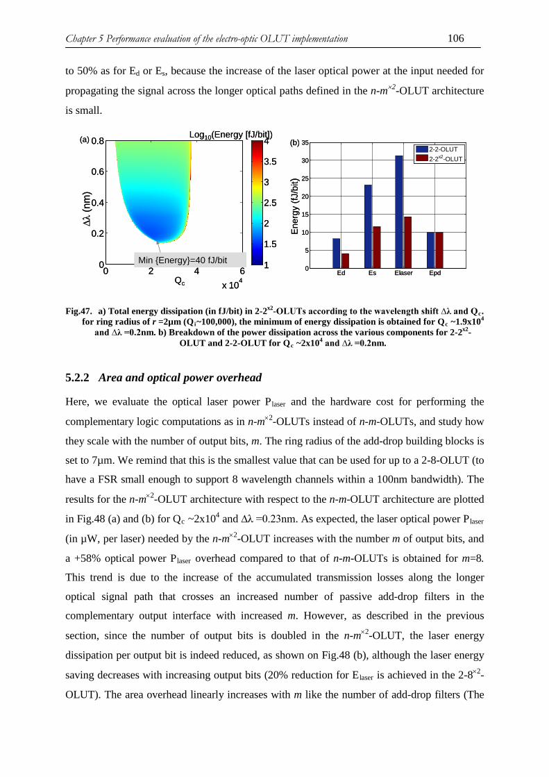
Chapter 5 Performance evaluation of the electro-optic OLUT implementation 106
to 50% as for Ed or Es, because the increase of the laser optical power at the input needed for
propagating the signal across the longer optical paths defined in the n-m×2-OLUT architecture
is small.
Ene
rgy
(fJ/b
it)
(b)
0 2 4 6x 10⁴
0
0.2
0.4
0.6
0.8
1
1.5
2
2.5
3
3.5
4Log10(Energy [fJ/bit])
∆λ(n
m)
Qc
(a)
Min {Energy}=40 fJ/bitEd Es Elaser Epd
0
5
10
15
20
25
30
35
2-2-OLUT2-2x2-OLUT
Ene
rgy
(fJ/b
it)
(b)
0 2 4 6x 10⁴
0
0.2
0.4
0.6
0.8
1
1.5
2
2.5
3
3.5
4Log10(Energy [fJ/bit])
∆λ(n
m)
Qc
(a)
Min {Energy}=40 fJ/bitEd Es Elaser Epd
0
5
10
15
20
25
30
35
2-2-OLUT2-2x2-OLUT
Fig.47. a) Total energy dissipation (in fJ/bit) in 2-2x2-OLUTs according to the wavelength shift ∆λ and Qc. for ring radius of r =2µm (Qi~100,000), the minimum of energy dissipation is obtained for Qc ~1.9x10⁴
and ∆λ =0.2nm. b) Breakdown of the power dissipation across the various components for 2-2x2-OLUT and 2-2-OLUT for Qc ~2x10⁴ and ∆λ =0.2nm.
5.2.2 Area and optical power overhead
Here, we evaluate the optical laser power Plaser and the hardware cost for performing the
complementary logic computations as in n-m×2-OLUTs instead of n-m-OLUTs, and study how
they scale with the number of output bits, m. The ring radius of the add-drop building blocks is
set to 7µm. We remind that this is the smallest value that can be used for up to a 2-8-OLUT (to
have a FSR small enough to support 8 wavelength channels within a 100nm bandwidth). The
results for the n-m×2-OLUT architecture with respect to the n-m-OLUT architecture are plotted
in Fig.48 (a) and (b) for Qc ~2x10⁴ and ∆λ =0.23nm. As expected, the laser optical power Plaser
(in µW, per laser) needed by the n-m×2-OLUT increases with the number m of output bits, and
a +58% optical power Plaser overhead compared to that of n-m-OLUTs is obtained for m=8.
This trend is due to the increase of the accumulated transmission losses along the longer
optical signal path that crosses an increased number of passive add-drop filters in the
complementary output interface with increased m. However, as described in the previous
section, since the number of output bits is doubled in the n-m×2-OLUT, the laser energy
dissipation per output bit is indeed reduced, as shown on Fig.48 (b), although the laser energy
saving decreases with increasing output bits (20% reduction for Elaser is achieved in the 2-8×2-
OLUT). The area overhead linearly increases with m like the number of add-drop filters (The

Chapter 5 Performance evaluation of the electro-optic OLUT implementation 107
surface occupied by the add-drop filters is estimated to be 0.004mm2 by assuming each
microring is of 7µm radius). These results show that a reasonable optical laser power and area
overhead costs do exist for doubling the computation capacity of an OLUT through using the
n-m×2-OLUT architecture.
2 4 6 80
50
100
150
200
250
2-m-OLUT2-mx2-OLUT
2 4 6 80
20
40
60
80
100
120
140
2-m-OLUT2-mx2-OLUT
P las
er(µ
W)
E las
er(fJ
/bit)
mm
(a) (b)
(c)
2 4 6 80.04
0.06
0.08
0.1
0.12
0.14
0.16
0.18
2-m-OLUT2-mx2-OLUT
m
Area
(mm
2 )
+23%
+22%
+21%
+18%
+58% -20%
2 4 6 80
50
100
150
200
250
2-m-OLUT2-mx2-OLUT
2 4 6 80
20
40
60
80
100
120
140
2-m-OLUT2-mx2-OLUT
P las
er(µ
W)
E las
er(fJ
/bit)
mm
(a) (b)
(c)
2 4 6 80.04
0.06
0.08
0.1
0.12
0.14
0.16
0.18
2-m-OLUT2-mx2-OLUT
m
Area
(mm
2 )
+23%
+22%
+21%
+18%
+58% -20%
Fig.48. Comparison of the (a) input optical power for each laser Plaser (b) laser energy dissipation per output Elaser and (c) total area of OLUT according to the number of lasers m between 2-m-OLUTs
(represented by blue square) and 2-mx2-OLUTs (represented by red star) for a ring radius= 7µm, Qc ~2x10⁴ and ∆λ =0.23nm. [Laser differential efficiency=90%, Supply voltage = 1V][169]
5.2.3 Case study: a 1-bit ALU implemented by a n-mx2-OLUT
Similarly to the performance evaluation for the n-m-OLUT, a real computation case i.e.
1-bit ALU is implemented here by the n-m×2-OLUT architecture. In this specific case, we

Chapter 5 Performance evaluation of the electro-optic OLUT implementation 108
compare this configuration with the n-m-OLUT to highlight the benefits of the complementary
output in energy dissipation, area occupation and hardware efficiency.
Fig.49 illustrates the implementation relying on the proposed 2-5×2-OLUT architecture
with complementary output bits. Similar to the implementation proposed in the last section,
the logic operations of ADD, SUBTRACT and OR are realized by λ0, λ1, λ2, λ3 respectively.
However, the operations of NAND, NOR, X OR (not Y), NXOR and not Y are computed by
the complementary output bits using the wavelength λ0, λ1, λ2, λ3 and λ4, respectively. Since
each wavelength produces two logic output bits, only 5 optical laser signals are needed for
implementing all the logic functions of such an ALU application. Consequently, a 44%
reduction of the number of active add-drop filters is achieved in the memorization part (36
required in the 2-9-OLUT with respect to 20 for the 2-5×2-OLUT plus 5 passive rings). The
minimum energy dissipation of 30fJ/bit is obtained for Qc ~4.4x10⁴ and ∆λ =0.13nm which
corresponds to a ~43% improvement compared to the minimum of the 2-9-OLUT (53fJ/bit,
for Qc ~4.5x10⁴ and ∆λ =0.14nm). This is firstly due to the reduction of the number of active
add-drop filters in the Through-state in the memorization part i.e. 9 in the 2-5×2-OLUT with
respect to 18 in the 2-9-OLUT (as previously mentioned the add-drops related to the
complementary part are passive and do not dissipate any static energy). As a result, a 58%
reduction for the total static energy dissipation of the add-drop filters Es is achieved in this
case (23fJ/bit and 9.6fJ/bit for 2-9-OLUT and 2-5×2-OLUT respectively). Moreover, a total
saving of 60% for the laser energy dissipation is achieved in the n-m×2-OLUT due to the fact
that a reduced number of laser sources are used (16.5fJ/bit and 6.8fJ/bit for the 2-9-OLUT and
the 2-5×2-OLUT respectively). In addition, the dynamic energy consumption of the add-drop
filters is the same for both OLUTs since their routing parts are the same. Table 4 summarizes
the comparison results.
YX
1
Routing part Memorization part
1 1
0
0
0
1
0
λx
λx
λx
D D D D
0 λ0
λ0
λ0
λ0
λ1
λ1
1 λ1
0 λ2
λ2
λ2
λ3
1 λ3
0 λ3
~(XY)Y
X+Y }
Carry Sum (Difference)
X-Y
Borrow
}
X or ~Y ~(X or Y)X or Y
0 λ2
~(X xor Y)
D
1 λ3
0 λ1
D D D D
λ0
λ1
λ1
λ1
λ2
λ2 λ3
λ3
λ0
λ0
λ0 λ1
λ2
λ2 λ3
λ3
~YD
λ4
λ4
λ4
λ4
1
1
λ4
0 λ4
λ4
0 λ4
Complementary part
5 lasers
Fig.49. 1-bit ALU implemented with n-m×2-OLUT

Chapter 5 Performance evaluation of the electro-optic OLUT implementation 109
Therefore, we can conclude that the n-m×2-OLUT allows us to perform the logic
computation with a reduced number of optical devices, hence achieving a significant reduction
of energy dissipation and area occupation of an ALU application compared with the n-m-
OLUT architecture implementation.
Tab 4. Comparison of a 1-bit ALU implemented by n-m-OLUT and n-m-×2OLUT
2-9-OLUT 2-5×2-OLUT
Number of output bits 9 10
Number of laser channels 9 5 (-44%)
Total number of add-drop filters 39 28 (-28%)
OLUT size (mm2) 0.156 0.11 (-29%)
Minimum total energy dissipation 53 fJ/bit 30 fJ/bit ( -43%)
5.3 Conclusions
This chapter focused on the system-level performance evaluation for the electro-optic
OLUT architectures by using the multi-level modelling approach and the physical
implementation proposed in Chapter 4. The numerical results show the potential of the
resulting OLUT architectures to reach <100 fJ/bit logic operation. In addition, we
demonstrated the potential of n-m×2-OLUT architectures for improving the hardware and
energy efficiency of n-m-OLUTs through the implementation example of a 1-bit ALU. The
analytical results highlight the key advantage of complementary outputs to increase the
computation capacity of an OLUT up to 100% for a reasonable overhead of input optical laser
power and area occupation.

Chapter 5 Performance evaluation of the electro-optic OLUT implementation 110

Chapter 6 Conclusions and Perspectives 111
Chapter 6 CONCLUSIONS AND PERSPECTIVES
6.1 Conclusions
In the data explosion era, our world is becoming more information-intensive.
Continuing to provide better computing systems is a key enabler of the information and
communication innovations that bring profound and far-reaching changes into our world. Due
to the ever-increasing demand for high-performance, cost-effective, energy-economic
computing hardware and the difficulty of satisfying these conflicting requirements using
conventional or incremental approaches, new computing paradigms relying on emerging
technologies are needed.
Beyond the use of silicon photonics in the realization of communication channels in
multi-core processor architectures, optical technology could also be exploited to perform
some parts of computing in an all-optical way, thus benefiting from the intrinsic advantages of
light for achieving computation with potentially high bandwidth and low power consumption.
However, it is illusory to consider that optics can directly compete with electronics based
computing, due to the technological immaturity leading to issues for integration, reliability
and low-cost manufacturing and its intrinsically large size. To make optics suitable for filling
a useful role in niche functions to help future computing systems operate better and more
efficiently, it is mandatory to rethink and redesign the computing architecture and its
constituent building blocks to make the most of the properties of light. Some useful guidelines
for developing computing architectures with optical technologies are summarized as follows:
a) the computation has to remain in the optical domain as much as possible, and the use of
electro-optic interface should be limited; b) the use of the light spectrum and WDM for
representing and processing information in parallel is a fundamental vector for creating
powerful computing architectures with reduced energy consumption and hardware resources;
c) the optical hardware must be flexible to evolve with the evolution of the computing
application, which is achievable by using reconfigurable computing paradigm; d) and most
importantly, optics should be used with the objective of improving the energy efficiency of
computing systems.
In light of these guidelines, in this thesis we have proposed a new reconfigurable
optical logic architecture, the optical lookup table (OLUT), which is an optical core
Chapter 6 Conclusions and Perspectives 112
implementation of a lookup table. Currently, advances in the design of high-performance
silicon chips for reconfigurable computing, e.g. Field Programmable Gate Arrays (FPGAs),
rely on CMOS technology and are essentially limited by energy consumption. As CMOS
technologies approach their fundamental scaling limits, traditional approaches in increasing
FPGA computational power will ultimately lead to higher heat generation and more stringent
power/area requirements. It is therefore impossible for the pJ/bit performance indicator to
continue to decrease indefinitely with each technology generation. Alternatively, silicon
photonics, as a key enabling technology that has matured significantly over the years, has the
potential to help break the performance/power barrier in FPGAs and close the performance
gap between FPGAs and ASICs. By using a mature CMOS fabrication process, this
technology can benefit from highly integrated assembly techniques with most components
fabricated on the CMOS platform, thus greatly reducing the manufacturing cost.
The proposed OLUT architecture accelerates logic computation by making the full
advantages of the light spectrum through WDM. It offers significant improvement in latency
and energy consumption with respect to state-of-the-art optical logic architectures, e.g.
directed logic architectures, through allowing the use of WDM technology for parallel
computation. The principle of the OLUT architecture was presented through a basic OLUT
block with single output, which performs logic operations as an electronic LUT. Using a
number of multiplexed wavelengths, the basic OLUT block was generalized to produce
multiple output bits in parallel for realizing different Boolean functions simultaneously. The
performance of this architecture was qualitatively evaluated through the example of a 1-bit
full adder. When compared to RDL circuits in this full adder configuration, OLUTs allow for
lower latency and a reduced number of lasers and photodetectors, hence reducing the energy
consumption and increasing the computation speed. In addition, the OLUT architecture was
further extended by exploring the complementary logic interface, which enables higher
computation capacity and lower energy-per-bit over the initial OLUT architecture with
reasonable area and hardware overhead.
The OLUT architecture is, to a certain extent, technology independent. The OLUT
architecture and concept presented in chapter 3 could be physically implemented using a
variety of approaches, which would certainly impact the performance of the resulting
computing architecture. We proposed one specific physical implementation for OLUTs,
which might not be optimal but takes advantages of mature silicon photonics technology. In
this implementation, we focused on the realization of electro-optic OLUTs, i.e. where the

Chapter 6 Conclusions and Perspectives 113
input and output data remain in the electrical domain. We developed and implemented an
embodiment of its building block, i.e. an electrically-controlled microring-resonator based
optical add-drop filter that fully meets the functional needs of routing and filtering optical
wavelength channels in the OLUT architecture. A critical drawback of this proposal is
associated with the electro-optic approach, which needs O/E conversions to cascade OLUTs.
The other main drawback of this choice is that the silicon microring resonators are
temperature sensitive devices because the spectral width of its resonance wavelengths is
narrow (~0.1nm for a ring with Q~15000), and silicon has a large thermo-optical coefficient.
Temperature control is therefore needed for maintaining the state of the ring resonators during
the operation of the OLUTs. Indeed, in a photonic system using WDM scheme, wavelength
tuning is essential to compensate for fabrication non-uniformity and varying operating
environments, which was not taken into account in the estimation of the power consumption
for the OLUT in Chapter 5. Another limitation that arises from the specific implementation
choice is the speed limit at which the electro-optic switches that were introduced in Chapter 4
can be run (because these switches built from PIN junction using carrier injection scheme).
However, there are many other ways of implementing the add-drop filter, e.g. directional
coupler, photonic crystals or MZI interferometer, and as technology advances, more compact,
energy-efficient and cost-economic devices become available. It is worth noting that the
landscape of silicon photonics is moving extremely fast with new integrated devices reported
every year. Our modeling work does not however rely on new breakthroughs in device
performance, i.e. speed, power or efficiency. Instead we focused on investigating how some
mature silicon photonic devices (hereby electrically driven silicon microring-resonator based
add-drop filters) should be designed for the OLUT computing architecture to reach system-
level performance requirements. In this context, we have also proposed a multi-level
modeling approach based on design space exploration of device parameters to estimate the
system performance. This method allows us to study the feasibility of the OLUT architecture
and explore the design space of silicon photonic devices for performing reliable and efficient
computation in OLUT architectures. As such, this method could therefore be extended to
evaluate the performance of OLUTs relying on different physical implementations, simply by
changing the physical model used at the device level.
The performance evaluation for electro-optic OLUT architectures was presented by
using the multi-level approach and the physical model. The impact of the OLUT input
dimensions on the device parameters, and consequently on the system energy efficiency is

Chapter 6 Conclusions and Perspectives 114
studied by calculating the feasible design space for OLUTs. The analytical results showed the
potential of OLUT architectures to reach <100 fJ/bit logic operation, which is indeed
comparable to the total energy dissipation per logic operation for current silicon CMOS
devices (i.e. at the femtojoule level, according to ITRS [5]). In addition, we illustrated the
potential of the n-m×2-OLUT architecture for improving the hardware and energy efficiency
with respect to the n-m-OLUT through the implementation of a 1-bit Arithmetic Logic Unit
(ALU). The analytical results highlighted the key advantage of complementary outputs to
increase the computation capacity of an OLUT up to 100% for a reasonable overhead in input
optical laser power and area occupation. However, it should be pointed out that the proposed
model does not include some energy dissipation sources associated with that should be well
taken into account in a real environment, e.g. the static energy consumption for lasers, the
thermal energy required by the add-drop filters for pre-calibration and real-time thermal
tuning. In particular, this implementation of the OLUT (ring-based silicon photonics) is
sensitive to temperature, and that thermal tuning could potentially be a showstopper here.
However, it should be stressed that the main contributions of the PhD are (i) the concept of
the OLUT itself (independent of the implementation) and (ii) the design and evaluation
methodology used to quantify the performance metrics. In order to push the analysis as far as
possible, we used ring-based silicon photonics (as do most other works on photonic
computing architectures, e.g. directive logic, and for which these pre-calibration problems are
common to all). This choice, with the degree of accuracy that can be reached for the ring
diameter in current technologies, does make this pre-calibration power hungry. However, it
should be pointed out that the 1pJ/bit used by us in section 4.3 as a rough estimation of the
order of magnitude is a worst case value reached by assuming the largest fabrication error for
all the rings (i.e. all rings require maximum tuning). As previously indicated, the value can
and should be decorrelated from the OLUT concept itself - it fully depends on how the
architecture is implemented. Other, more prospective, implementation types exist (Mach-
Zehnder, directive couplers, photonic crystals), and more rigorous evaluations of how to
quantify and reduce the calibration energy should be a future topic of work.
Furthermore, reminding that the two main contributions to the energy dissipation of
OLUT architectures are energy dissipated within lasers and add-drop filters, two different
directions can be exploited to further improve the energy consumption figure for the OLUT
architectures such as: i) exploring more compact and energy-efficient add-drop filters built
from less mature (nano)technologies, such as nano-resonator devices [179,182], very small
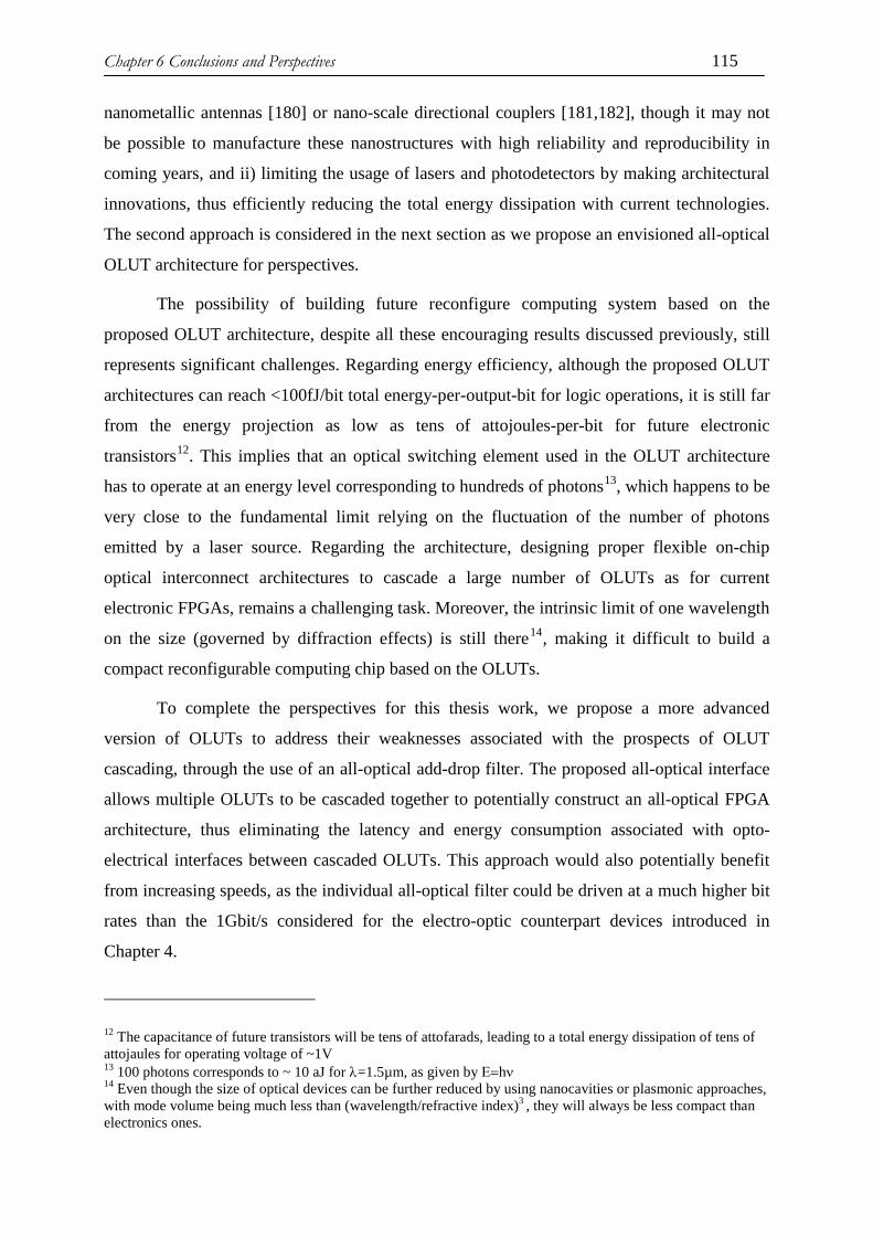
Chapter 6 Conclusions and Perspectives 115
nanometallic antennas [180] or nano-scale directional couplers [181,182], though it may not
be possible to manufacture these nanostructures with high reliability and reproducibility in
coming years, and ii) limiting the usage of lasers and photodetectors by making architectural
innovations, thus efficiently reducing the total energy dissipation with current technologies.
The second approach is considered in the next section as we propose an envisioned all-optical
OLUT architecture for perspectives.
The possibility of building future reconfigure computing system based on the
proposed OLUT architecture, despite all these encouraging results discussed previously, still
represents significant challenges. Regarding energy efficiency, although the proposed OLUT
architectures can reach <100fJ/bit total energy-per-output-bit for logic operations, it is still far
from the energy projection as low as tens of attojoules-per-bit for future electronic
transistors12. This implies that an optical switching element used in the OLUT architecture
has to operate at an energy level corresponding to hundreds of photons13, which happens to be
very close to the fundamental limit relying on the fluctuation of the number of photons
emitted by a laser source. Regarding the architecture, designing proper flexible on-chip
optical interconnect architectures to cascade a large number of OLUTs as for current
electronic FPGAs, remains a challenging task. Moreover, the intrinsic limit of one wavelength
on the size (governed by diffraction effects) is still there14, making it difficult to build a
compact reconfigurable computing chip based on the OLUTs.
To complete the perspectives for this thesis work, we propose a more advanced
version of OLUTs to address their weaknesses associated with the prospects of OLUT
cascading, through the use of an all-optical add-drop filter. The proposed all-optical interface
allows multiple OLUTs to be cascaded together to potentially construct an all-optical FPGA
architecture, thus eliminating the latency and energy consumption associated with opto-
electrical interfaces between cascaded OLUTs. This approach would also potentially benefit
from increasing speeds, as the individual all-optical filter could be driven at a much higher bit
rates than the 1Gbit/s considered for the electro-optic counterpart devices introduced in
Chapter 4.
12 The capacitance of future transistors will be tens of attofarads, leading to a total energy dissipation of tens of attojaules for operating voltage of ~1V 13 100 photons corresponds to ~ 10 aJ for λ=1.5µm, as given by Ε=hν 14 Even though the size of optical devices can be further reduced by using nanocavities or plasmonic approaches, with mode volume being much less than (wavelength/refractive index)3 , they will always be less compact than electronics ones.

Chapter 6 Conclusions and Perspectives 116
6.2 A possible all-optical implementation of OLUTs: towards all-optical FPGAs
The all-optical OLUT design is based on the concept of using optically controlled
switches in the routing part of OLUTs, and inputs and outputs sharing the same (optical) data
representation, enabling the cascade of multiple OLUTs to realize complex functions without
requiring electro-optical or opto-electronic conversions that are fundamentally dissipative in
energy and relatively slow [111]. We choose the optically controlled switches driven by
injecting free carriers through the use of an optical signal. Note that many other optical
nonlinear effects (in higher orders) can be considered to implement these switching elements,
e.g. two-photon absorption, optical Kerr effect etc., which will be a future topic of this work.
The main issue of this proposition is that the design and fabrication of all-optical switches is
far from mature, leading to a limited utilization of wavelength combs and increased design
complexity.
6.2.1 Cascading of OLUTs
Fig.50 depicts the example of two identical 1-2-OLUTs in cascade to illustrate the
basic principle of a possible all-optical OLUT implementation. In this scenario, the input data
stream x0 of OLUTA is carried by the λ1 wavelength, which tunes the optically controlled
switch into the Through-state by injecting free carriers into the device’s active region via a
high-intensity optical signal. In the absence of this control signal, the switches of the routing
part remain in the Drop-state. The behavior of such a switching element in the routing part is
illustrated in Fig.51(a) according to its Drop- and Through- state. The optical control signal
needs to be amplified and spectrally shifted (from λ1 to λc) in the preceding OLUT block
before reaching the optically controlled add-drop filters of OLUTA, as illustrated in Fig.51 (b).
It is worth noting that the wavelength of the control signal indeed needs to be slightly
different from the switch resonant wavelengths due to the electro-refractive effect (although
how big this spectral shift might be for optimal performance of OLUT will not be discussed
here). In addition, only a part of the control signal will be absorbed inside the device region,
which causes an additional optical power output at λc that is transferred at the DROP port.
Hence, in Fig.50, the optical signals λ0 λ1 injected from the laser sources on the left will
propagate through the Through port on the bottom waveguide (note that a small fraction of
the control signal will still drop into the other waveguide, without further effect on the OLUT
behavior) and will eventually drop to an output port Zi when crossing a Drop-state switch in
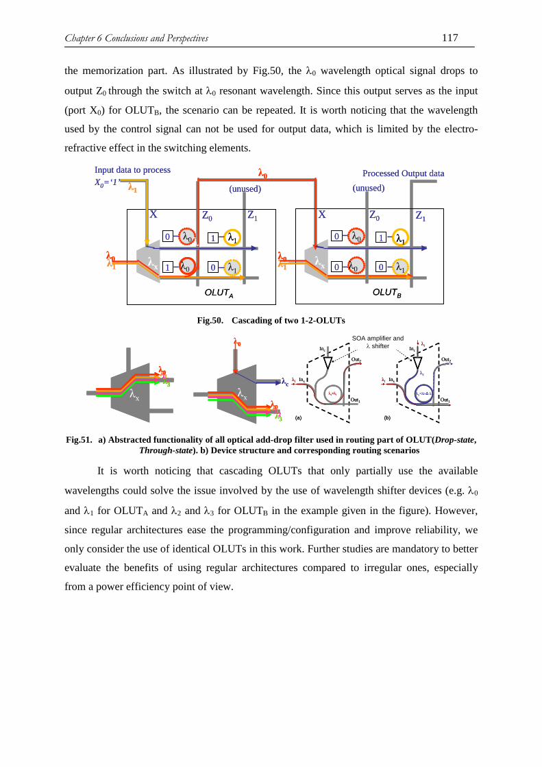
Chapter 6 Conclusions and Perspectives 117
the memorization part. As illustrated by Fig.50, the λ0 wavelength optical signal drops to
output Z0 through the switch at λ0 resonant wavelength. Since this output serves as the input
(port X0) for OLUTB, the scenario can be repeated. It is worth noticing that the wavelength
used by the control signal can not be used for output data, which is limited by the electro-
refractive effect in the switching elements.
OLUTA
X
1
0
0
1
λx
λ0
λ0 λ1
λ1
λ0λ1
X0=‘1’
λx
λ0λ1
OLUTB
X
0
0
0
1
λx
λ0
λ0 λ1
λ1
λ0λ1
Z0 Z0Z1 Z1
Input data to process Processed Output data
(unused) (unused)
OLUTA
X
1
0
0
1
λx
λ0
λ0 λ1
λ1
λ0λ1
X0=‘1’
λx
λ0λ1
OLUTB
X
0
0
0
1
λx
λ0
λ0 λ1
λ1
λ0λ1
Z0 Z0Z1 Z1
Input data to process Processed Output data
(unused) (unused)
Fig.50. Cascading of two 1-2-OLUTs
λx
λ1λ2λ3
λ0
λxλ1λ2λ3
λ0
λ0
λc
λx
λ1λ2λ3
λ0
λx
λ1λ2λ3
λ0
λxλ1λ2λ3
λ0
λ0
λc
Out1
Out2
(a)
λi
λx=λi
EDFA amplifier and λ shifterInc
Ins
Out1
Out2
(b)
λi
λx=λi-Δ λ
Inc
Ins
λi
λc
SOA amplifier and λ shifter
Out1
Out2
(a)
λi
λx=λi
EDFA amplifier and λ shifterInc
Ins
Out1
Out2
(b)
λi
λx=λi-Δ λ
Inc
Ins
λi
λc
SOA amplifier and λ shifter
Fig.51. a) Abstracted functionality of all optical add-drop filter used in routing part of OLUT(Drop-state, Through-state). b) Device structure and corresponding routing scenarios
It is worth noticing that cascading OLUTs that only partially use the available
wavelengths could solve the issue involved by the use of wavelength shifter devices (e.g. λ0
and λ1 for OLUTA and λ2 and λ3 for OLUTB in the example given in the figure). However,
since regular architectures ease the programming/configuration and improve reliability, we
only consider the use of identical OLUTs in this work. Further studies are mandatory to better
evaluate the benefits of using regular architectures compared to irregular ones, especially
from a power efficiency point of view.
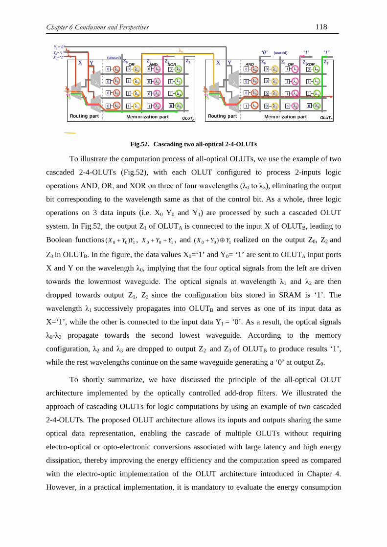
Chapter 6 Conclusions and Perspectives 118
OLUTA
YX0
Routing part Memorization part
1
0 1
0
0
0
0 0
0
1
0
1
1
λx
λx
λ0
λ0
λ0
λ0
λ1
λ1
λ1
λ1 λ2
λ2
λ2
λ2
λ3
1 λ3
λ3
0 λ3
λ0λ1λ2λ3
X0=‘1’
λx
Y0=‘1’ λ0
λ0
YX0
Routing part Memorization part
0
1 1
0
1
1
1 0
0
0
0
0
0
λx
λx
λ0
λ0
λ0
λ0
λ1
λ1
λ1
λ1 λ2
λ2
λ2
λ2
λ3
1 λ3
λ3
0 λ3
λ0λ1λ2λ3
λx
Y1=‘0’
Z0 Z1 Z2 Z3OR AND XOR AND OR XOR
‘0’ ‘1’‘1’Z0 Z1 Z2 Z3
OLUTB
(unused)
λ1 (unused)
OLUTA
YX0
Routing part Memorization part
1
0 1
0
0
0
0 0
0
1
0
1
1
λx
λx
λ0
λ0
λ0
λ0
λ1
λ1
λ1
λ1 λ2
λ2
λ2
λ2
λ3
1 λ3
λ3
0 λ30 λ3
λ0λ1λ2λ3
X0=‘1’
λx
Y0=‘1’ λ0
λ0
YX0
Routing part Memorization part
0
1 1
0
1
1
1 0
0
0
0
0
0
λx
λx
λ0
λ0
λ0
λ0
λ1
λ1
λ1
λ1 λ2
λ2
λ2
λ2
λ3
1 λ3
λ3
0 λ30 λ3
λ0λ1λ2λ3
λx
Y1=‘0’
Z0 Z1 Z2 Z3OR AND XOR AND OR XOR
‘0’ ‘1’‘1’Z0 Z1 Z2 Z3
OLUTB
(unused)
λ1 (unused)
Fig.52. Cascading two all-optical 2-4-OLUTs
To illustrate the computation process of all-optical OLUTs, we use the example of two
cascaded 2-4-OLUTs (Fig.52), with each OLUT configured to process 2-inputs logic
operations AND, OR, and XOR on three of four wavelengths (λ0 to λ3), eliminating the output
bit corresponding to the wavelength same as that of the control bit. As a whole, three logic
operations on 3 data inputs (i.e. X0 Y0 and Y1) are processed by such a cascaded OLUT
system. In Fig.52, the output Z1 of OLUTA is connected to the input X of OLUTB, leading to
Boolean functions 100 )( YYX + , 100 YYX ++ , and 100 )( YYX ⊕+ realized on the output Z0, Z2 and
Z3 in OLUTB. In the figure, the data values X0=‘1’ and Y0= ‘1’ are sent to OLUTA input ports
X and Y on the wavelength λ0, implying that the four optical signals from the left are driven
towards the lowermost waveguide. The optical signals at wavelength λ1 and λ2 are then
dropped towards output Z1, Z2 since the configuration bits stored in SRAM is ‘1’. The
wavelength λ1 successively propagates into OLUTB and serves as one of its input data as
X=‘1’, while the other is connected to the input data Y1 = ‘0’. As a result, the optical signals
λ0-λ3 propagate towards the second lowest waveguide. According to the memory
configuration, λ2 and λ3 are dropped to output Z2 and Z3 of OLUTB to produce results ‘1’,
while the rest wavelengths continue on the same waveguide generating a ‘0’ at output Z0.
To shortly summarize, we have discussed the principle of the all-optical OLUT
architecture implemented by the optically controlled add-drop filters. We illustrated the
approach of cascading OLUTs for logic computations by using an example of two cascaded
2-4-OLUTs. The proposed OLUT architecture allows its inputs and outputs sharing the same
optical data representation, enabling the cascade of multiple OLUTs without requiring
electro-optical or opto-electronic conversions associated with large latency and high energy
dissipation, thereby improving the energy efficiency and the computation speed as compared
with the electro-optic implementation of the OLUT architecture introduced in Chapter 4.
However, in a practical implementation, it is mandatory to evaluate the energy consumption

Chapter 6 Conclusions and Perspectives 119
associated with the additional amplifiers and wavelength-shifter devices, which may reduce
the gain of the elimination of the electro/optic interface in the resulting all-optical OLUT
architecture.
6.2.2 Interconnect network
Generally speaking, interconnecting reconfigurable cells remains a tedious task since,
on one hand, the network is supposed to give the required flexibility to the architecture to
execute any application, while on the other hand, it is also responsible for the high power
consumption and low operating frequency. In this work, our objective is not to reach the
routing flexibility available in today’s FPGA. It is rather to concentrate on fixed (i.e. non-
configurable) networks to interconnect OLUTs executing data-intensive applications in an
efficient way. For this purpose, a streaming-like model of computation is considered; in this
model, data propagate in a single direction and are successively processed by different
operations. Using this model of computation will not require the management of optical signal
propagation in the opposite direction, which helps to reduce the network complexity.
Furthermore, the interconnect also needs to exploit WDM to route optical signals
efficiently. Many Optical Networks on Chip (ONoC) relying on WDM were proposed in the
past few years [109,114,123]. However, in most cases, the data routing is dynamic and
depends on the traffic between processors and memories, which is not suitable to interconnect
OLUTs, since FPGA architectures rely on fixed interconnects once a configuration is applied.
The solution is to use a passive interconnect structure. For this purpose, we consider i)
ORNoC and ii) λ-router networks. Both networks are contention-free (which do not need
arbitration) with high throughput and low latency. They are composed of passive photonic
switching elements. The following gives the main guidelines to interconnect OLUTs through
these networks.
6.2.2.1 ORNoC
Each OLUT interfaces with ORNoC through an Optical Network Interface (ONI),
which performs the following three operation modes:
Ejection: the incoming optical signal on a waveguide is redirected to an OLUT input.
This is achieved by a microresonator located along the waveguide and with the same resonant
wavelength as the signal;

Chapter 6 Conclusions and Perspectives 120
Pass through: the incoming signal propagates along the waveguide (i.e. no
microresonator with the same resonant wavelength is located on the waveguide);
Injection: OLUT injects an optical signal into a waveguide through its output port
data.
The main feature of ORNoC is that the same wavelength can be used to realize
multiple communications on the same waveguide, at the same time, according to application-
specific data dependencies. Consequently, fewer waveguides are required and scalability is
improved. While the ORNoC waveguides are supposed to be rolled back in our prior work (i.e.
as ring), this is not mandatory for interconnecting OLUTs (i.e. straight waveguides are
considered). Furthermore, multiple waveguides can be used to propagate the optical signals
through the network, and multiple waveguides can be used to interface OLUT with an ONI.
Fig.53 (a) illustrates an example where two waveguides cross four ONI, each ONI being
connected to inputs and outputs of an OLUT through two waveguides.
6.2.2.2 λ-router The λ−router is a multistage network relying on WDM to propagate optical signals
from input to output ports. In the proposed architecture, multiple λ-routers are successively
connected to each other and each λ-router input (resp. output) port is connected to an OLUT
output (resp. input) port through a single waveguide. A reduction method can be used to
reduce the network complexity by managing only the required optical connections. Fig.53 (b)
illustrates a simple example where 6 OLUTs are interconnected through two λ-router
networks.
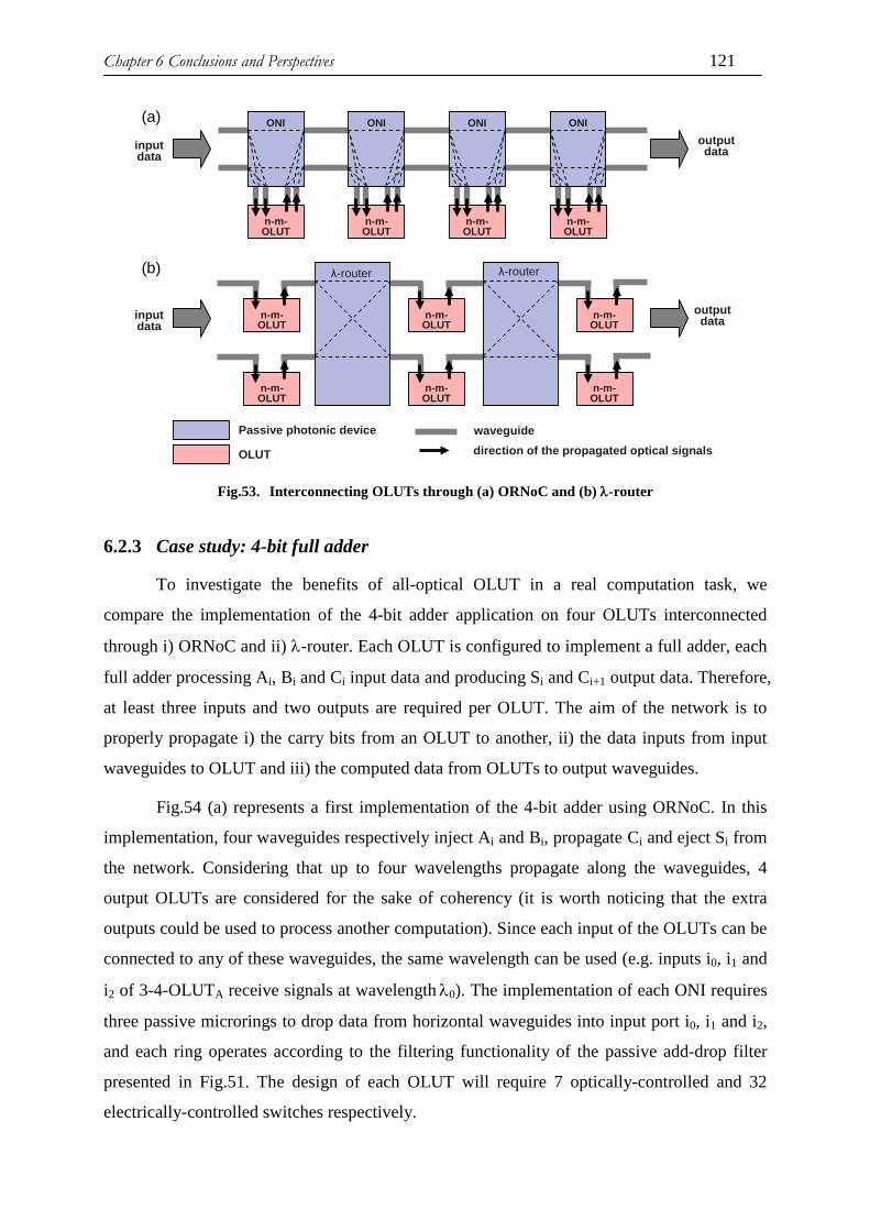
Chapter 6 Conclusions and Perspectives 121
inputdata
outputdata
inputdata
outputdata
(a)
(b)
Passive photonic device
OLUT
waveguide
λ-routerλ-router
n-m-OLUT
ONI
n-m-OLUT
ONI
n-m-OLUT
ONI
n-m-OLUT
ONI
n-m-OLUT
n-m-OLUT
n-m-OLUT
n-m-OLUT
n-m-OLUT
n-m-OLUT
direction of the propagated optical signals
Fig.53. Interconnecting OLUTs through (a) ORNoC and (b) λ-router
6.2.3 Case study: 4-bit full adder
To investigate the benefits of all-optical OLUT in a real computation task, we
compare the implementation of the 4-bit adder application on four OLUTs interconnected
through i) ORNoC and ii) λ-router. Each OLUT is configured to implement a full adder, each
full adder processing Ai, Bi and Ci input data and producing Si and Ci+1 output data. Therefore,
at least three inputs and two outputs are required per OLUT. The aim of the network is to
properly propagate i) the carry bits from an OLUT to another, ii) the data inputs from input
waveguides to OLUT and iii) the computed data from OLUTs to output waveguides.
Fig.54 (a) represents a first implementation of the 4-bit adder using ORNoC. In this
implementation, four waveguides respectively inject Ai and Bi, propagate Ci and eject Si from
the network. Considering that up to four wavelengths propagate along the waveguides, 4
output OLUTs are considered for the sake of coherency (it is worth noticing that the extra
outputs could be used to process another computation). Since each input of the OLUTs can be
connected to any of these waveguides, the same wavelength can be used (e.g. inputs i0, i1 and
i2 of 3-4-OLUTA receive signals at wavelength λ0). The implementation of each ONI requires
three passive microrings to drop data from horizontal waveguides into input port i0, i1 and i2,
and each ring operates according to the filtering functionality of the passive add-drop filter
presented in Fig.51. The design of each OLUT will require 7 optically-controlled and 32
electrically-controlled switches respectively.

Chapter 6 Conclusions and Perspectives 122
Fig.54 (b) illustrates a second implementation relying on three λ-routers. The generic
structure from Fig.54 (b) was reduced to replace unused OLUTs by simple waveguides, which
suits well the simple carry propagation application. The structure of each λ-router was further
reduced to only manage optical signals requiring their propagation direction to be modified(i.e.
the carries, as represented by dashed lines in the figure). The main difference with the first
implementation relies on the use of a single waveguide to interface OLUT inputs with the
network port, thus requiring the use of distinct wavelengths for i0, i1 and i2. Hence, since
fewer wavelengths are required to represent the initial data (three compared to four with
ORNoC), two additional wavelengths must be considered to process Si and Ci+1 data, thus
resulting in larger 3-5-OLUTs. Their design thus requires 8 additional electrically controlled
switches compared to the former implementation. While the ejection of data from waveguides
also requires three passive microrings per OLUT, the design of the λ-router itself requires 2
additional passive devices to redirect the carries signals.
The early design complexity comparison thus gives a small advantage to the ORNoC
based implementation. However, further comparisons (including the execution of additional
applications) through relevant key metrics (e.g. power and performances) are mandatory and
will be carried out in future work.
ONID
3-4-OLUTD
i0 i1 i2 o2 o3o1o0
ONIC
3-4-OLUTC
i0 i1 i2 o2 o3o1o0
ONIB
i0 i1 i2 o2 o3o1o0
ONIA
3-4-OLUTA
i0 i1 i2 o2 o3o1o03-4-OLUTB
S0 S1 S2 S3
Cout
A0A1A2A3B0
B1B2B3
Cin
i0 i1 i2 o2 o3o1o0
(a)
A0
A1
A2
A3
B0
B1
B2
B3
Cin
3-5-OLUTA
i0 i1 i2 o2 o3o1o0 o4
3-5-OLUTB
i0 i1 i2 o2 o3o1o0 o43-5-OLUTC
i0 i1 i2 o2 o3o1o0 o4
3-5-OLUTD
i0 i1 i2 o2 o3o1o0 o4
S0
S1
S2
S3 Coutλ-routerA λ-routerB λ-routerC(b)
Fig.54. Implementation of the 4-bit full adder application on four OLUTs interconnected through (a)
ORNoC and (b) λ-routers
Both implementations share the main advantage of providing coherent data
representations. Indeed, in ORNoC, the injected set of data (e.g. A0…A4) and processed data
propagate along the same waveguide with different wavelengths. For the implementation

Chapter 6 Conclusions and Perspectives 123
using λ-routers, the same data set propagates through different waveguides but with the same
wavelength (e.g. λ 0 for the above-mentioned example). This allows the assembly of further
OLUTs to process more complex applications.
6.2.4 Discussion
The proposed all-optical architectures are made realistic by the critical property of
controlling the propagation of optical signals by another optical signal. Without this property,
electrical-to-optical and optical-to-electrical conversions would be required. While we
considered a device relying on a microring resonator, other structures (e.g. Photonic Crystals
[121]) demonstrated equivalent behavior at higher speed, higher integration level (2x~4x) but
also leading to a more technological challenging fabrication process [121]. Further advances
in the physical demonstration of devices with the above mentioned properties are still
mandatory to improve the energy efficiency and the performance of the proposed
architectures significantly.
At the system level, interconnecting even a small number of OLUTs is already a
challenging task due to the various existing design options such as the number and the size of
OLUTs and the network complexity (e.g. number of waveguides and number of wavelengths).
Design space exploration is thus mandatory to identify the best design tradeoffs, mainly
according to power efficiency and performance metrics. However, this exploration requires
automated tools for mapping application benchmarks (e.g. MCNC[117]), taking into account
the main advantage of OLUTs, i.e. the parallel computation on a same set of data. The
implementation of such tool is part of future works.
The last key point to be addressed in future work is the use of optical memories as
registers or buffer in the application data paths. This is a necessary step to execute FIR-filter
like signal processing applications on an all-optical FPGA. Although optical buffers [122]
have been realized in some work, their performance and operating conditions are far from
satisfactory. The main issue is still the design of high-performance low-cost optical devices
for memories or buffers. Apart from this, further design space exploration is again mandatory
to evaluate if such optical memories are appropriate to be located on OLUT output ports (as it
is the case in FPGA) or in dedicated systems.

Chapter 6 Conclusions and Perspectives 124

References 125
REFERENCES
1. “21st century computer architecture, a community white paper”, May 2012
(http://csl.stanford.edu/~christos/publications/2012.21stcenturyarchitecture.whitepaper.
pdf)
2. R. Ho, K. W. Mai, and M. A. Horowitz, “The future of wires”, Proc. IEEE 89, 490–
504, (2001).
3. J.L. Manferdelli et al., “Challenges and opportunities in many-core computing”, Proc.
IEEE 96,5 2008
4. Moore, Gordon E. "Cramming more components onto integrated circuits." 1965
5. International Technology Roadmap for Semiconductors (ITRS). http://www.itrs.net/
(2013) Documents available at this website describe in detail the current state of the art
in integrated circuits and near-term milestones.
6. M. Azimi, N. Cherukuri, D. N. Jayasimha, A. Kumar, P. Kundu, S. Park, I. Schoinas,
and A. S. Vaidya, “Integration challenges and tradeoffs for terascale architectures”, J.
Intel Technol. 11(3), (2007).
7. JD Meindl et al., “Limits on silicon nanoelectronics for Terascale integration”, Science,
293, 2044-2049, 2001
8. “Optics and photonics: essential technologies for our nation”, US Research Council
report 2013
9. Taubenblatt, M. A, “Optical Interconnects for High-Performance Computing”, J. of
Lightwave technology, 30(4), 448-457,2012
10. K Bergman et al., Exascale computing study: technology challenges in achieving
exascale computing, 2008
11. “Why choose multi-mode fiber?”
http://www.corning.com/docs/opticalfiber/cn0603.pdf
12. Beausoleil, Ray, et al. “A nanophotonic interconnect for high-performance many-core
computation”, Integrated Photonics and Nanophotonics Research and Applications.
Optical Society of America, 2008

References 126
13. D.A.B Miller, “Device Requirements for Optical Interconnects to Silicon Chips” Proc.
IEEE 97(7), 1166-1185, (2009).
14. Harnessing Light: Optical Science and Engineering for the 21st Century by National
Research Council, National Academy Press, Washington, DC, 1998
15. P. Ambs, “Optical computing: a 60-year adventure,” Adv. Opt. Technol. 2010, 372652
(2010).
16. N. Kirman, M. Kirman, R. K. Dokania, J. F. Martinez, A. B. Apsel, M. A. Watkins, D.
H. Albonesi, “Leveraging Optical Technology in Future Bus-based Chip
Multiprocessors”, in Proc. IEEE/ACM Micro., pp.492-503, (2006)
17. M Asghari et al., “silicon photonics: energy-efficient communication” Nature
photonics 5, 268-270 (2011)
18. A. Shacham, K. Bergman, and L. P. Carloni, “Photonic networks-on-chip for future
generations of chip multiprocessors”, IEEE Trans. Comput. 57, 1246–1260, (2008).
19. A. F. Benner, M. Ignatowski, J. A. Kash, D. M. Kuchta, and M. B. Ritter, “Exploitation
of optical interconnects in future server architectures”, IBM J. Res. Develop. 49 (4/5),
755–775 (2005).
20. S. Le Beux, et al. “Layout Guidelines for 3D Architectures including Optical Ring
Network-on-Chip (ORNoC)”. In 19th IFIP/IEEE VLSI-SOC International Conference,
2011
21. P. J. van Heerden, “Theory of optical information storage in solids,” Applied Optics,
vol. 2, no. 4, pp. 393–400, 1963.
22. L. K. Anderson, “Holographic optical memory for bulk data storage,” Bell
Laboratories Records, vol. 46, pp. 318–325, 1968.
23. A. Vander Lugt, “Holographic memories,” in Optical Information Processing, Y. E.
Nesterkhin, G. W. Stroke, and W. E. Kock, Eds., pp. 347–368, Plenum Press, New
York, NY, USA,1976.
24. P. J. Marchand, A. V. Krishnamoorthy, K. S. Urquhart, et al., “Motionless-head
parallel readout optical-disk system,” Applied Optics, vol. 32, no. 2, pp. 190–203,
1993.
25. F. H. Mok, G. W. Burr, and D. Psaltis, “Angle and space multiplexed holographic
random access memory (HRAM),” Optical Memory and Neural Networks, vol. 3, no.
2, pp. 119–127, 1994.
References 127
26. J. Ashley, M. P. Bernal, G. W. Burr, et al., “Holographic data storage,” IBM Journal of
Research and Development, vol. 44,no. 3, pp. 341–368, 2000.
27. “In Phase Technolgies Products,” 2009, http://www.inphase-technologies.com/.
28. S. Hunter, F. Kiamilev, S. Esener, et al., “Potentials of two-photon based 3-D optical
memories for high performance computing,” Applied Optics, vol. 29, no. 14, pp. 2058–
2066,1990.
29. B. Kohler, S. Bernet, A. Renn, et al., “Storage of 2000 holograms in a photochemical
hole burning system,” Optics Letters, vol. 18, no. 24, pp. 2144–2146, 1993.
30. H. J. Coufal, D. Psaltis, and G. T. Sincerbox, Holographic DataStorage, Springer,
Berlin, Germany, 2000.
31. H. J. Caulfield, “Perspectives in optical computing,” Computer, vol. 31, no. 2, pp. 22–
25, 1998.
32. H. J. Caulfield and S. Dolev, “Why future supercomputing requires optics,” Nat.
Photonics 4 (5), 261–263 (2010).
33. D. A. B. Miller, “Are optical transistors the logical next step,” Nat. Photonics 4 (1), 3–
5 (2010).
34. J. G Hardy, and J. Shamir, “Optics inspired logic architecture,” Opt. Express 15(1),
150–165 (2007).
35. K.T Vandoorne, P. Mechet, T. Van Vaerenbergh, M. Fiers, G. Morthier, D.
Verstraeten, B. Schrauwen, J. Dambre, P. Bienstman, Experimental demonstration of a
reservoir computing on a silicon photonics chip, Nature Communications, 5, p.1-6
(2014)
36. M.J.Callaghan et al. “Highly integrated compact optical correlators using FLC-VLSI
spatial light modulators and diffractive optics”, Proc. SPIE 3289, Micro-Optics
Integration and Assemblies, 1998
37. Chase C, Serrano J, Ramadge P J. Periodicity and chaos from switched flow systems:
contrasting examples of discretely controlled continuous systems. Automatic Control,
IEEE Transactions on, 1993, 38(1): 70-83
38. P. Ambs, W. E. Cleland, D. E. Kraus, P. Suni, J. A. Thompson, and J. Turek,
“Kinoform filter for an incoherent optical processor,” Applied Optics, vol. 22, no. 6,
pp. 796–803, 1983

References 128
39. W. E. Cleland, D. E. Kraus, J. A. Thompson, and P. Ambs, “Optical trigger processor
for high energy physics,” Nuclear Instruments & Methods in Physics Research, vol.
216, no. 3, pp. 405–414, 1983
40. S. Bains, “Miniature optical correlator fits inside a PC,” Laser Focus World, vol. 31,
no. 12, pp. 17–18, 1995
41. H. Rajbenbach, Y. Fainman, and S. H. Lee, “Optical implementation of an iterative
algorithm for matrix inversion,” Applied Optics, vol. 26, no. 6, pp. 1024–1031, 1987.
42. H. J. Caulfield, W. T. Rhodes, M. J. Foster, et al., “Opticalimplementation of systolic
array processing,” Optics Communications vol. 40, no. 2, pp. 86–90, 1981.
43. D. Psaltis, D. Brady, and K. Wagner, “Adaptive optical networks using photorefractive
crystals,” Applied Optics, vol. 27, no. 9, pp. 1752–1759, 1988
44. F. B. McCormick, F. A. P. Tooley, T. J. Cloonan, et al.,“Experimental investigation of
a free-space optical switching network by using symmetric self-electro-optic-effect
devices,” Applied Optics, vol. 31, no. 26, pp. 5431–5446, 1992
45. P. S. Guilfoyle and R. V. Stone, “Digital optical computer II,” in Optical
Enhancements to Computing Technology, vol.1563 of Proceedings of SPIE, pp. 214–
222, 1991
46. R.S. Kudokas et al. “A digital optical implementation of RISC”, IEEE Compcon
Spring '91. Digest of Papers pp.436-441, San Francisco, 1991
47. L. J. Cutrona, E. N. Leith, C. J. Palermo, et al., “Optical data processing and filtering
systems,” IRE Transactions on Information Theory, vol. 6, no. 3, pp. 386–400, 1960
48. C. S. Weaver and J. W. Goodman, “A technique for optically convolving two
functions,” Applied Optics, vol. 5, no. 7, pp. 1248–1249, 1966.
49. A. Vander Lugt, “Coherent optical processing,” Proceedings of the IEEE, vol. 62, no.
10, pp. 1300–1319, 1974
50. T. H.Maiman, “Stimulated optical radiation in ruby,” Nature, vol. 187, no. 4736, pp.
493–494, 1960.
51. J. D. Armitage and A. W. Lohmann, “Character recognition by incoherent spatial
filtering,” Applied Optics, vol. 4, no. 4, pp. 461–467, 1965.
52. E. N. Leith, “The evolution of information optics,” IEEE Journal on Selected Topics in
Quantum Electronics, vol. 6, no.6, pp. 1297–1304, 2000
53. D. K. Pollock, C. J. Koester, and J. T. Tippett, Optical Processing of Information,
Spartan Books, Baltimore, Md,USA, 1963

References 129
54. R. Tessier and W. Burleson, “Reconfigurable computing and digital signal processing:
a survey”, Journal of VLSI Signal Processing, Vol. 28, pp. 7–27, May/June 2001,
55. T.J.Todman et al., “Reconfigurable Computing: Architectures and Design Methods”,
IEE Proc. Computers & Digital Techniques, 2004
56. Ron Wilson, FPGAs in 2032: the ACM FPGA 2012 workshop
57. www.xilinx.com
58. Altera Cooperation, White Paper. “Accerating high performance computing with
FPGAs.” October 2007
59. Bondalapti, K., & Prasanna,V. Reconfigurable computing systems. Proceedings of the
IEEE, Vol. 90, No. 7, July, 2002.
60. Buell, D., El-Ghazawi, T., Gaj,K. & Kindratenko,V, “High-Performance
reconfigurable computing”. IEEE Computer Society, March, 2007.
61. El-Ghazawi, T., El-Araby, E., Miaoqing Huang, Gaj,K., Kindratenko, V. & Buell, D.
“The promise of high-performance reconfigurable computing”. IEEE computer society,
February, 2008 pp. 69 -76.
62. Guneysu,T., Paar,C., Pelzl,J., Pfieffer,G., Schimmler,M., & Schlieffer,C. “Parallel
computing with low cost FPGAs A framework for COPACOBANA”.
63. Herbordt, M.C., VanCourt, T., Yongfeng, G., Shukhwani, B., Conti,A., Model,J. &
Disabello,D. “ Achieving high performance with FPGA-Based computing”
64. Smith, M.C., Vetter,J.S., & Alam,S.R. “Scientific computing beyond CPUs: FPGA
implementations of common scientific kernels.” MAPLD/187.
65. Todman,T.J., Constantinides, G.A., Wilton,S.J.E, Luk,W. & Cheung, P.Y.K. “
Reconfigurable computing: architectures and design methods.” IEEE Proceedings of
Computer Digital Technologies, Vol. 152, No. 2, March, 2005.
66. F. LI et al., “Vdd programmability to reduce FPGA interconnect power” DAC04, 2004
67. I. Kuon and J. Rose, “Measuring the gap between FPGAs and ASICs,” IEEE Trans.
Comput.-Aided Des. Integr. Circuits Syst., vol. 26, no. 2, pp. 203–215, Feb. 2007
68. T. Tuan and B. Lai, “Leakage power analysis of a 90 nm FPGA,” in Proc. IEEE
Custom Integr. Circuits Conf., San Jose, CA, pp.57–60. 2003
69. F. Li, D. Chen, L. He, and J. Cong, “Architecture evaluation for power-efficient
FPGAs,” in Proc. ACM/SIGDA Int. Symp. Field Program. Gate Arrays, Monterey,
CA, pp. 175–184. 2003

References 130
70. A. Rahman and V. Polavarapuv, “Evaluation of low-leakage design techniques for
field-programmable gate arrays,” in Proc. ACM/SIGDA Int. Symp. Field Program.
Gate Arrays, Monterey, CA, 2004, pp. 23–30.
71. L. Shang, A. Kaviani, and K. Bathala. “Dynamic Power Consumption inthe Virtex-II
FPGA Family”. In: ACM/SIGDA International Symposium on Field Programmable
Gate Arrays, pp. 157–164, Monterey, CA, 2002
72. K. Poon, A. Yan, and S. J. E. Wilton, “A flexible power model for FPGAs,” in Proc.
Int. Conf. Field-Program. Logic Appl., Montpellier, France, 2002, pp. 312–321.
73. J. Anderson and F. Najm. “Power Estimation Techniques for FPGAs”. IEEE
Transactions on Very Large Scale Integration (VLSI) Systems, Vol. 12, No. 10, pp.
1015–1027, Oct. 2004.
74. D. Chen, J. Cong, and Y. Fan. “Low-Power High-Level Synthesis for FPGA
Architectures”. In: ACM/IEEE International Symposium on Low-Power Electronics
and Design, pp. 134–139, Seoul, Korea, 2003.
75. Ahmed Sharkawy, Dennis W. Prather et al., “Chip-scale photonic interconnects for
reconfigurable computing”, Proc. SPIE 7609, Photonic and Phononic Crystal Materials
and Devices, 2010
76. Kawahara et al., “2mb spin-transfer torque RAM (SPRAM) with bit-by-bit
bidirectional currentwrite and parallelizing-direction current read. In Proceedings of the
International Solid-State Circuits Conference. IEEE, Los Alamitos, CA, 480–482
77. W.Zhao et al., “Spin Transfer Torque (STT)-MRAM–Based Runtime Reconfiguration
FPGA Circuit”. ACM Transactions on Embedded Computing Systems, Vol. 9, No. 2
2009
78. Khoonbani F, Jahanian A. Improved performance and power consumption of three-
dimensional FPGAs using Carbon Nanotube interconnects. 16th IEEE CSI
International Symposium on Computer Architecture and Digital Systems (CADS),
pp.25-30, 2012
79. Guillemenet Y, Torres L, Sassatelli G. “Non-volatile run-time field-programmable gate
arrays structures using thermally assisted switching magnetic random access
memories”. IET Computers & Digital Techniques, 4(3): 211-226. 2010
80. www.Xilinx.com
81. www.Altera.com

References 131
82. Y. Guillemenet, L. Torres, G. Sassatelli, and I. Hassoune. “A nonvolatile run-time
FPGA using thermally assisted switching MRAMs”. In International Conference on
Field Programmable Logic and applications, 2008
83. O. Goncalves et al. Non-Volatile FPGAs based on Spintronic Devices, DAC13, 2013
84. Yang, J. Joshua, Dmitri B. Strukov, and Duncan R. Stewart. "Memristive devices for
computing." Nature nanotechnology 8.1, 13-24, 2013
85. Smullen C W, Mohan V, Nigam A, et al. “Relaxing non-volatility for fast and energy-
efficient STT-RAM caches” 2011 IEEE 17th International Symposium on High
Performance Computer Architecture (HPCA), 50-61, 2011
86. Zhou P, Zhao B, Yang J, et al. “Energy reduction for STT-RAM using early write
termination”, Computer-Aided Design-Digest of Technical Papers, ICCAD
IEEE/ACM International Conference on. 264-268.2009
87. Gilbert, Nad, et al. "A 0.6 V 8 pJ/write Non-Volatile CBRAM Macro Embedded in a
Body Sensor Node for Ultra Low Energy Applications." VLSI Circuits (VLSIC), 2013
Symposium on. IEEE, 2013.
88. Miyamura, Makoto, et al. "Programmable cell array using rewritable solid-electrolyte
switch integrated in 90nm CMOS." Solid-State Circuits Conference Digest of
Technical Papers (ISSCC), 2011.
89. Z. Zhiping, W. Yi, H. S. P. Wong, and S. S. Wong, "Nanometer-Scale HfOx RRAM,"
Electron Dev. Lett., vol. 34, pp. 1005-1007, Aug. 2013
90. L. Tz-Yi, et al., "A 130.7mm2 2-layer 32Gb ReRAM memory device in 24nm
technology," in ISSCC Dig. of Tech. Papers, pp. 210-211, 2013
91. Panasonic Starts World's First Mass Production of ReRAM Mounted Microcomputers.
Available: http://panasonic.co.jp/corp/news/official.data/data.dir/2013/07/en130730-
2/en130730-2.html
92. L. Goux, et al., Roles and Effects of TiN and Pt Electrodes in Resistive-Switching
HfO2 Systems, Electrochemical and Solid-State Letters, vol. 14, pp. H244-H246, June
2011
93. T.Naito et al., World's first monolithic 3D-FPGA with TFT SRAM over 90nm 9 layer
Cu CMOS. IEEE Symposium on. VLSI Technology (VLSIT), 2010.
94. W. R. Davis, J. Wilson, S. Mick, et al., Demystifying 3D ICs: the pros and cons of
going vertical. IEEE Design and Test of Computers, 22(6):498–510, 2005
95. Emerging research architectures, ITRS 2013

References 132
96. L. Madden, et al., "Advancing High Performance Heterogeneous Integration Through
Die Stacking", Proc. ESSCIRC, pp. 18-24, Sept. 2012
97. Sun G, Chen Y, Dong X, et al. Three-dimensional Integrated Circuits: Design, EDA,
and Architecture. Foundations and Trends in Electronic Design Automation, 2011,
5(1–2): 1-151.
98. M. J. Alexander, J. P. Cohoon, J. L. Colesh, et al., Three-dimensional field-
programmable gate arrays. In Proc. Eighth Annual IEEE Int. ASIC Conf. and Exhibit,
pages 253-256, 1995.
99. M. Leeser, W. M. Meleis, M. M. Vai, S. Chiricescu, W. Xu, and P. Rothko: a three-
dimensional fpga. IEEE Design & Test of Computers, 15(1), pp.16-23, 1998.
100.S. M. S. A. Chiricescu and M. M. Vai. A three-dimensional fpga with an integrated
memory for in-application reconguration data. In Proc. IEEEInt. Symp. Circuits and
Systems ISCAS '98, volume 2, pages 232-235, 1998.
101.A. Rahman, S. Das, and et al. Wiring requirement and three-dimensional integration
technology for field programmable gate arrays. TVLSI, 11(1):44-54, 2003.
102.M. Lin, A. El Gamal, and et al. Performance benefits of monolithically stacked 3-D
FPGA. TCAD, 26(2), 216-229, 2007.
103.A. Gayasen, V. Narayanan, M. Kandemir, and A. Rahman. Designing a 3-d fpga:
Switch box architecture and thermal issues. IEEE Transactions on Very Large Scale
Integration (VLSI) Systems, 16(7),882-893, 2008.
104. C. Ababei, P. Maidee, and K. Bazargan. Exploring potential benefits of 3D FPGA
integration. In FPL, 2004
105. Pan Y, Zhang T. DRAM-based FPGA enabled by three-dimensional (3d) memory
stacking. In Proceedings of the 18th annual ACM/SIGDA international symposium on
Field Programmable Gate Arrays, 290, 2010
106. Overcome Copper Limits with Optical Interfaces, white paper, Altera corporation
April 2011
107. J. Rose, R.J. Francis, D. Lewis and P. Chow, “Architecture of Programmable Gate
Arrays: The Effect of Logic Block Functionality on Area Efficiency,” IEEE J. Solid
State Circuits, pp. 1217-1225, 1990
108. Z. Li, S. Le Beux, C. Monat, X. Letartre, I.O’Connor, “Optical Look Up Table”, in
Proc. of DATE, pp.483-486, 2013

References 133
109. A. Shacham et al., “Photonic Network-on-Chip for Future Generations of Chip Multi
Processors,” IEEE Trans. Computers, vol. 57, no. 9, pp. 1246-1260, Sept. 2008
110. S. Le Beux et al., “Reconfigurable photonic switching: Towards all-optical FPGAs”,
in Proc. VLSI-SoC, pp.180-185, 2013.
111. J. Hardy, and J. Shamir, “Optics Inspired Logic Architecture,” Opt. Express 15(1),
150–165 (2007).
112. Q. Xu and R. Soref, “Reconfigurable optical directed-logic circuits using
microresonator-based optical switches,” Opt. Express 19(6), 5244–5259, (2011).
113. A.W.Poon et al., “Cascaded microresonator-based matrix switch for silicon on-chip
optical interconnection”. Proc. IEEE, 97(7), pp.1216-1236, 2009
114. I. O’Connor, et al. “Reduction Methods for Adapting Optical Network on Chip
Topologies to Specific Routing Applications”. In Proceedings of DCIS, November
2008.
115. G.T. Reed, et al., “Silicon optical modulators” ,Nature Photonics 4, 518 – 526, 2010
116. S. Manipatruni et al. “High speed carrier injection 18 Gb/s silicon micro-ring electro-
optic modulator”. IEEE Proc.Lasers and Electro-Optics Soc. 537–538, 2007
117. BLIF ISCAS’89 and MCNC benchmarks, http://cadlab.cs.ucla.edu/~kirill/
118. V. R. Almeida, C. A. Barrios, R. R. Panepucci, and M. Lipson, "All-optical control of
light on a silicon chip," Nature 431, 1081-1084 , 2004
119. Q. Xu and M.Lipson, “All-optical logic based on silicon micro-ring resonators”, Opt.
Express, vol. 15, no. 3, pp. 924-929, 2007
120. Y. Vlasov, W Green and F. Xia, “High-throughput silicon nanophotonic wavelength
insensitive switch for on-chip optical networks”, Nature Photonics 2, 242 – 246, 2008
121. R. Soref et al.“Optical add-drop filters based on photonic crystal ring resonators” ,Opt.
Express, vol. 15, no.4, pp.1823-1831, 2007
122. F. Xia et al. “Ultracompact optical buffers on a silicon chip”, Nature photonics, vol.1,
pp.65-71, 2007
123. Y. Ye et al. “A Torus-based Hierarchical Optical-Electronic Network-on-Chip for
Multiprocessor System-on-Chip”, ACM Journal on Emerging Technologies in
Computing Systems, 2012.
124. S. Le Beux, et al. “Layout Guidelines for 3D Architectures including Optical Ring
Network-on-Chip (ORNoC)”. In 19th IFIP/IEEE VLSI-SOC International Conference,
2011
References 134
125. L.Vivien, A.Polzer, D.Marris-Morini, J.Osmond, J.M. Hartmann, P.Crozat, E. Cassan,
C. Kopp, H. Zimmermann and J-M. Fédéli, “Zero-bias 40Gbit/s germanium waveguide
photodetector on silicon”, Opt. Express 20(2), 1096–1101 (2012).
126. B. E. Nelson, G. A. Keeler, D. Agarwal, N. C. Helman and D. A. B. Miller,
“Wavelength division multiplexed optical interconnect using short pulses”, IEEE
J.Sel.Top. Quantum Electron.9, 486–491 (2003).
127. Q. Xu, S. Manipatruni, B. Schmidt, J. Shakya, and M. Lipson, “12.5 Gbit/s carrier-
injection-based silicon micro-ring modulators”, Opt. Express 15, 430–436, (2007).
128. B. G. Lee, B. A. Small, Q. Xu, M. Lipson, and K. Bergman, “Characterization of a
4x4 Gb/s parallel electronic bus to WDM optical link silicon photonic translator”,
IEEE Photon. Technol. Lett.19, 456–458, (2007).
129. R. A. Soref and B. R. Bennett, “Electrooptical Effects in Silicon," IEEE J. Quantum
Electron. 23 (1), 123-129, (1987).
130. http://optics.synopsys.com/rsoft/
131. C. Manolatou, M.J. Khan, S. Fan, P.R. Villeneuve, H.A. Haus, J.D. Joannopoulos,
“Coupling of Modes Analysis of Resonant Channel Add–Drop Filters”, IEEE J.
Quantum Electron, 35 (9), 1322-1331, 1999.
132. B.E. Little, S.T. Chu, H.A.Haus, J. Foresi, and J.-P. Laine. Microring resonator
channel dropping filters. Journal of Lightwave Technology, 15(6), 998–1005, 1997
133. E.F. Schubert, Light Emitting Diode (Cambridge University Press, 2006).
134. J. Zhou, M. J. O’Mahony, and S. D. Walker, “Analysis of optical crosstalk effects in
multi-wavelength switched networks,” IEEE Photon.Technol. Lett. 6, 302–305, (1994).
135. Ian O’Connor, F. Tissafi-Drissi, F. Gaffiot, J. Dambre, M. De Wilde, J. Van
Campenhout, D. Van Thourhout, D. Stroobandt, “Systematic Simulation-Based
Predictive Synthesis of Integrated Optical Interconnect”, IEEE Transactions on Very
Large Scale Integration (VLSI) Systems 15(8), 927-940, (2007).
136. B. Ramamurthy, D. Datta, H. Feng, J.P. Heritage, B. Mukherjee, “Impact of
transmission impairments on the teletraffic performance of Wavelength-Routed Optical
Networks,” J. Lightwave Technol. 17, 1713-1723 (1999).
137. L. Chen, P. Dong, and M. Lipson, “Integrated GHz silicon photonic interconnect with
micrometer-scale modulators and detectors”, Opt. Express 17(17), 15248-15256, 2009.

References 135
138. M. Borselli, T. J. Johnson, and O. Painter, “Beyond the Rayleigh scattering limit in
high-Q silicon microdisks: theory and experiment,” Opt. Express 13(5), 1515-1530
2005.
139. M. Lipson, “Compact electro-optic modulators on a silicon chip”, IEEE J. Sel. Top.
Quantum Electron.12 (6), 1520–1526, 2006.
140. S. Goliaei and S. Jalili, "An optical wavelength-based computational machine",
International J. Unconventional Computing 9 (1-2), 97-123, (2013)
141. A. Biberman, B. G. Lee, K. Bergman, P. Dong, and M. Lipson, “Demonstration of all-
optical multi-wavelength message routing for silicon photonic networks,”. In OFC., pp.
1–3, February 2008.
142. D. Ding and D. Z. Pan, “OIL: A nano-photonics optical interconnect library for a new
photonic networks-on-chip architecture,” International workshop on System-Level
Interconnect Prediction, pp. 11–18, 2009
143. A.Poon et al., “Cascaded microresonator-based matrix switch for silicon on-chip
optical interconnection”. Proc. IEEE, 97(7), 1216-1236, 2009.
144. Ma Y, Zhang Y, Yang S, et al. “Ultralow loss single layer submicron silicon
waveguide crossing for SOI optical interconnect”. Optics Express, 21(24): 29374-
29382. 2010
145. Joannopoulos, J. D., Johnson, S. G., Winn, J. N., & Meade, R. D. Photonic crystals:
molding the flow of light. Princeton university press. 2011
146. Dai D, Yang L, He S. Ultrasmall thermally tunable microring resonator with a
submicrometer heater on Si nanowires. Journal of Lightwave Technology, 26(6), 704-
709, 2008
147. Van Campenhout J, Green W M J, Assefa S, et al. Integrated NiSi waveguide heaters
for CMOS-compatible silicon thermo-optic devices. Optics Letters, 35(7): 1013-1015,
2010.
148. Gunn C. “CMOS photonics for high-speed interconnects”. Micro, IEEE, 26(2): 58-66.
2006
149. N.Feng et al., “Vertical p-i-n germanium photodetector with high external responsivity
integrated with large core Si waveguides”, Opt. Express, 18(1), 96-101, 2010.
150. C.Qiu et al., Reconfigurable Electro-Optical Directed Logic Circuit Using Carrier
Depletion Micro-ring Resonators, Optics letters, 2014

References 136
151. Haus H A. Waves and fields in optoelectronics. Englewood Cliffs, NJ: Prentice-Hall,
1984.
152. Ziebell M, Marris-Morini D, Rasigade G, et al. 40 Gbit/s low-loss silicon optical
modulator based on a pipin diode. Optics express, 20(10), 10591-10596, 2012.
153. Teich M C, Saleh B E A. “Fundamentals of photonics.” Canada, Wiley Interscience,
1991.
154. F.Gan et al., “Maximizing the Thermo-Optic Tuning Range of Silicon Photonic
Structures”, PICS 2007
155. http://simple.wikipedia.org/wiki/Computer_architecture
156. Y. Patt, “Requirements, bottlenecks, and good fortune: agents for microprocessor
evolution”. Proceedings of the IEEE (2001).
157. Pocek, Tessier and DeHon, “Birth and Adolescence of Reconfigurable Computing: A
Survey of the First 20 Years of Field-Programmable Custom Computing Machines”
158. I. Kuon, et al. FPGA Architecture: Survey and Challenges
159. Masood, Adil, et al. "Comparison of heater architecture for thermal control of silicon
photonics circuits." IEEE Group IV Photonics 2013. 2013.
160. Ciyuan Qiu, Jie Shu, Zheng Li, Xuezhi Zhang, and Qianfan Xu. Wavelength tracking
with thermally controlled silicon resonators. Optics Express, 19(6), 5143–5148, 2011
161. Tessier, Russell, and Wayne Burleson. "Reconfigurable computing for digital signal
processing: A survey." Journal of VLSI signal processing systems for signal, image
and video technology 28.1-2 (2001): 7-27.
162. L. Cheng, F. Li, Y. Lin, P. Wong, and L. He, “Device and architecture cooptimization
for FPGA power reduction,” IEEE Transactions on Computer-Aided Design of
Integrated Circuits and Systems, vol. 26, no. 7, pp. 1211–1221, July 2007
163. Gilles Rasigade, PhD Thesis, Univ Paris-XI, 2010
164. F. Xia, M. Rooks, L. Sekaric, and Y. Vlasov, "Ultra-compact high order ring resonator
filters using submicron silicon photonic wires for on-chip optical interconnects," Opt.
Express, vol. 15, pp. 11934-11941,2007
165. V. Stojanovic, A. Joshi, C. Batten, K. Yong-jin, and K. Asanovic, "Manycore
processor networks with monolithic integrated CMOS photonics," in Lasers and
Electro-Optics, 2009 and 2009 Conference on Quantum electronics and Laser Science
Conference. CLEO/QELS 2009. Conference on, 2009, pp. 1-2

References 137
166. P. Dong, S. Liao, D. Feng, H. Liang, D. Zheng, R. Shafiiha, C.-C. Kung, W. Qian, G.
Li, X. Zheng, A. V. Krishnamoorthy, and M. Asghari, "Low Vpp, ultralow-energy,
compact, high-speed silicon electro-optic modulator," Opt. Express, vol. 17, pp. 22484-
22490, 2009
167. P.Dong, W.Qian, H.Liang et al. Low power and compact reconfigurable multiplexing
devices based on silicon microring resonators. Optics express, 2010, 18(10): 9852-
9858.
168. Chmielak B, Waldow M, Matheisen C, et al. Pockels effect based fully integrated,
strained silicon electro-optic modulator. Optics express, 2011, 19(18): 17212-17219.
169. A W. Fang et al., “A continuous-wave Hybrid AlGaInAs-Silicon Evanescent Laser”
IEEE Photonic Technology Letters, vol 18 no.10, 1143-1145, 2006
170. Erman Timurdogan et al., “An ultralow power athermal silicon modulator”, Nature
Communication 5, 4008, 2014
171. L. Vivien, J. Osmond, J. Fédéli, D. Marris-Morini, P. Crozat, J. Damlencourt, E.
Cassan, Y. Lecunff, and S. Laval, “42 GHz p.i.n Germanium photodetector integrated
in a silicon-on-insulator waveguide,” Opt. Express 17, 6252-6257 (2009)
172. Chen, Long, and Michal Lipson. "Ultra-low capacitance and high speed germanium
photodetectors on silicon." Optics Express 17.10 (2009): 7901-7906.
173. Selvaraja, shankar kumar, Bogaerts, W., Absil, P., Van Thourhout, D., & Baets, R.
(2010). Record low-loss hybrid rib/wire waveguides for silicon photonic circuits.
Presented at the 7th International conference on Group IV Photonics, New York, NY,
USA.
174. Shankar Kumar Selvaraja, Patrick Jaenen, Wim Bogaerts, Dries Van Thourhout, Pieter
Dumon, and Roel Baets. Fabrication of Photonic Wire and Crystal Circuits in Silicon-
on-Insulator Using 193-nm Optical Lithography. J. Lightwave Technol., 27(18), 4076–
4083, 2009
175. Peter Y. Yu, Manuel Cardona, “Fundamentals of Semiconductors: Physics and
Materials Properties”, pp.227-228, Springer, New York, 2005, ISBN 3-540-25470-6
176. D. Ahn, C. H. Hong, J. Liu, W. Giziewicz, M. Beals, L. C. Kimerling, J. Michel, J.
Chen, X. Kartner, High-performance, waveguide integrated Ge photodetectors Optics
Express, vol. 15, (7), pp. 3916–3921, 2007

References 138
177. Kristof Vandoorne, Joni Dambre, David Verstraeten, Benjamin Schrauwen, and Peter
Bienstman. Parallel reservoir computing using optical amplifiers. IEEE transactions on
neural networks, 22(9):1469–1481, 2011
178. Hideo Mabuchi, “Cavity-QED models of switches for attojoule-scale nanophotonic
logic,” Phys Rev A 80, 045802, (2009)
179. Tang, L. et al. Nanometre-scale germanium photodetector enhanced by a near-infrared
dipole antenna. Nature Photon. 2, 226–229 (2008)
180. Novotny, L., Van Hulst, N. Antennas for light, Nat. Photon., 5, pp.83–90, 2011
181. D. S. Ly-Gagnon, S. E. Kocabas, and D. A. B. Miller, “Characteristic impedance
model for plasmonic metal slot waveguides,” IEEE J. Sel. Top. Quantum Electron.
14(6), 1473–1478 (2008)
182. G. T. Reed, Silicon Photonics: The State of the Art (John Wiley & Sons, Ltd., 2008)
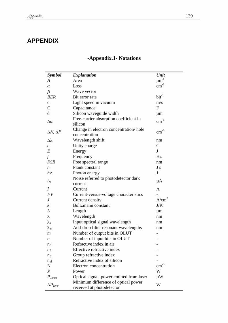
Appendix 139
APPENDIX
-Appendix.1- Notations
Symbol Explanation Unit A Area µm2 α Loss cm-1 β Wave vector BER Bit error rate bit-1 c Light speed in vacuum m/s C Capacitance F d Silicon waveguide width µm
∆α Free-carrier absorption coefficient in silicon cm-1
∆N, ∆P Change in electron concentration/ hole concentration cm-3
∆λ Wavelength shift nm e Unity charge C E Energy J f Frequency Hz FSR Free spectral range nm h Plank constant J s hv Photon energy J
iN Noise referred to photodetector dark current µA
I Current A I-V Current-versus-voltage characteristics - J Current density A/cm2 k Boltzmann constant J/K L Length µm λ Wavelength nm λi Input optical signal wavelength nm λx Add-drop filter resonant wavelengths nm m Number of output bits in OLUT - n Number of input bits in OLUT - n0 Refractive index in air - nf Effective refractive index - ng Group refractive index - nsi Refractive index of silicon - N Electron concentration cm-3 P Power W PLaser Optical signal power emitted from laser µW
∆Precv Minimum difference of optical power received at photodetector W

Appendix 140
qtot Total Electrical charge C Q Quality factor -
Qa Quality factor relate to carrier absorption loss -
QL Total (loaded) quality factor - Qi Intrinsic quality factor - Qc Coupling quality factor - r Ring radius µm ℜ Photodetector responsivity A/W R Resistance Ω t Time s t Amplitude decay time s T Temperature °C T11(V) Through port transmission - T21(V) Drop port transmission - τc Free-carrier lifetime s V Voltage V
Vop Operation voltage corresponding to the resonant state V
Note: This list does not contain some symbols that are used only in the section where they are defined
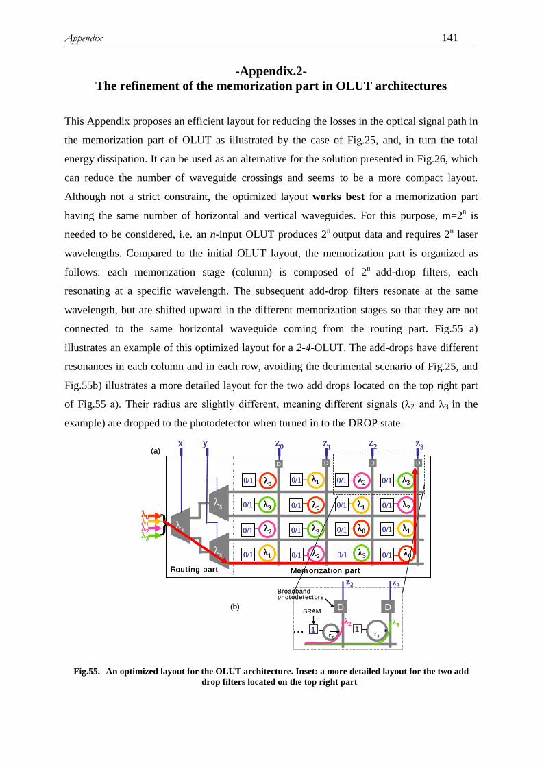
Appendix 141
-Appendix.2- The refinement of the memorization part in OLUT architectures
This Appendix proposes an efficient layout for reducing the losses in the optical signal path in
the memorization part of OLUT as illustrated by the case of Fig.25, and, in turn the total
energy dissipation. It can be used as an alternative for the solution presented in Fig.26, which
can reduce the number of waveguide crossings and seems to be a more compact layout.
Although not a strict constraint, the optimized layout works best for a memorization part
having the same number of horizontal and vertical waveguides. For this purpose, m=2n is
needed to be considered, i.e. an n-input OLUT produces 2n output data and requires 2n laser
wavelengths. Compared to the initial OLUT layout, the memorization part is organized as
follows: each memorization stage (column) is composed of 2n add-drop filters, each
resonating at a specific wavelength. The subsequent add-drop filters resonate at the same
wavelength, but are shifted upward in the different memorization stages so that they are not
connected to the same horizontal waveguide coming from the routing part. Fig.55 a)
illustrates an example of this optimized layout for a 2-4-OLUT. The add-drops have different
resonances in each column and in each row, avoiding the detrimental scenario of Fig.25, and
Fig.55b) illustrates a more detailed layout for the two add drops located on the top right part
of Fig.55 a). Their radius are slightly different, meaning different signals (λ2 and λ3 in the
example) are dropped to the photodetector when turned in to the DROP state.
Broadband photodetectors
yx
0/1
z0
Routing part Memorization part
z1
λ0
λ0
λ0
λ0
0/1
0/1
0/1
0/1
0/1
0/1
0/1
0/1
z2 z3
λ2
λ2
λ2
λ2
0/1
0/1
0/1
0/1
0/1
0/1
0/1 λ3
λ3
λ3
λ3
λ1
λ1
λ1
λ1
λx
λx
λx
}λ0λ1λ2λ3
D D D D
D
… 1
D
1λ2 λ3
SRAM
r2 r3
z3z2
(a)
(b)
Broadband photodetectors
yx
0/1
z0
Routing part Memorization part
z1
λ0
λ0
λ0
λ0
0/1
0/1
0/1
0/1
0/1
0/1
0/1
0/1
z2 z3
λ2
λ2
λ2
λ2
0/1
0/1
0/1
0/1
0/1
0/1
0/1 λ3
λ3
λ3
λ3
λ1
λ1
λ1
λ1
λx
λx
λx
}λ0λ1λ2λ3
λ0λ1λ2λ3
D D D D
D
… 1
D
1λ2 λ3
SRAM
r2 r3
z3z2
(a)
(b)
Fig.55. An optimized layout for the OLUT architecture. Inset: a more detailed layout for the two add drop filters located on the top right part
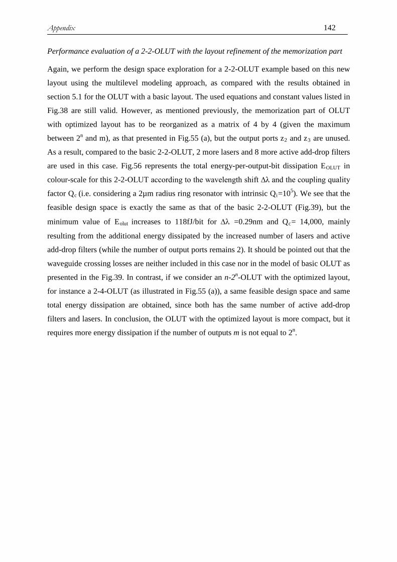
Appendix 142
Performance evaluation of a 2-2-OLUT with the layout refinement of the memorization part
Again, we perform the design space exploration for a 2-2-OLUT example based on this new
layout using the multilevel modeling approach, as compared with the results obtained in
section 5.1 for the OLUT with a basic layout. The used equations and constant values listed in
Fig.38 are still valid. However, as mentioned previously, the memorization part of OLUT
with optimized layout has to be reorganized as a matrix of 4 by 4 (given the maximum
between 2n and m), as that presented in Fig.55 (a), but the output ports z2 and z3 are unused.
As a result, compared to the basic 2-2-OLUT, 2 more lasers and 8 more active add-drop filters
are used in this case. Fig.56 represents the total energy-per-output-bit dissipation EOLUT in
colour-scale for this 2-2-OLUT according to the wavelength shift ∆λ and the coupling quality
factor Qc (i.e. considering a 2µm radius ring resonator with intrinsic Qi=105). We see that the
feasible design space is exactly the same as that of the basic 2-2-OLUT (Fig.39), but the
minimum value of Eolut increases to 118fJ/bit for ∆λ =0.29nm and Qc= 14,000, mainly
resulting from the additional energy dissipated by the increased number of lasers and active
add-drop filters (while the number of output ports remains 2). It should be pointed out that the
waveguide crossing losses are neither included in this case nor in the model of basic OLUT as
presented in the Fig.39. In contrast, if we consider an n-2n-OLUT with the optimized layout,
for instance a 2-4-OLUT (as illustrated in Fig.55 (a)), a same feasible design space and same
total energy dissipation are obtained, since both has the same number of active add-drop
filters and lasers. In conclusion, the OLUT with the optimized layout is more compact, but it
requires more energy dissipation if the number of outputs m is not equal to 2n.

Appendix 143
0 2 4 6x 10⁴
0
0.2
0.4
0.6
0.8
1
1.5
2
2.5
3
3.5
4Log10(Energy [fJ/bit])
∆λ(n
m)
Qc
Min {Energy}=118 fJ/bit
Feasible Design Space
0 2 4 6x 10⁴
0
0.2
0.4
0.6
0.8
1
1.5
2
2.5
3
3.5
4Log10(Energy [fJ/bit])
∆λ(n
m)
Qc
Min {Energy}=118 fJ/bit
Feasible Design Space
Fig.56. Feasible design space and the total energy dissipation in 2-2-OLUTs with the optimized layout according to ∆λ and Qc for ring radius of 2µm (Qi~100,000).

Appendix 144
Reconfigurable computing architecture exploration using silicon photonics technology
Abstract: Advances in the design of high performance silicon chips for reconfigurable computing, i.e. Field Programmable Gate Arrays (FPGAs), rely on CMOS technology and are essentially limited by energy dissipation. New design paradigms are mandatory to replace traditional, slow and power consuming, electronic computing architectures. Integrated optics, in particular, could offer attractive solutions. Many related works already addressed the use of optical on-chip interconnects to help overcome the technology limitations of electrical interconnects. Integrated silicon photonics also has the potential for realizing high performance computing architectures. In this context, we present an energy-efficient on-chip reconfigurable photonic logic architecture, the so-called OLUT, which is an optical core implementation of a lookup table. It offers significant improvement in latency and power consumption with respect to optical directed logic architectures, through allowing the use of wavelength division multiplexing (WDM) for computation parallelism. We proposed a multi-level modeling approach based on the design space exploration that elucidates the optical device characteristics needed to produce a computing architecture with high computation reliability (BER~10-18) and low energy dissipation. Analytical results demonstrate the potential of the resulting OLUT implementation to reach <100fJ/bit per logic operation, which may meet future demands for on-chip optical FPGAs. Key words: LUT, silicon photonics, WDM, design space exploration
Architecture de calcul reconfigurable en exploitant la technologie photonique sur silicium
Résumé: Les progrès dans la fabrication des systèmes de calcul reconfigurables de type « Field Programmable Gate Arrays » (FPGA) s’appuient sur la technologie CMOS, ce qui engendre une consommation des puces élevée. Des nouveaux paradigmes de calcul sont désormais nécessaires pour remplacer les architectures de calcul traditionnel ayant une faible performance et une haute consommation énergétique. En particulier, optique intégré pourrait offrir des solutions intéressantes. Beaucoup de travail sont déjà adressées à l’utilisation d’interconnexion optique pour relaxer les contraintes intrinsèques d’interconnexion électronique. Dans ce contexte, nous proposons une nouvelle architecture de calcul reconfigurable optique, la « optical lookup table » (OLUT), qui est une implémentation optique de la lookup table (LUT). Elle améliore significativement la latence et la consommation énergétique par rapport aux architectures de calcul d’optique actuelles tel que RDL (« reconfigurable directed logic »), en utilisant le spectre de la lumière au travers de la technologie WDM. Nous proposons une méthodologie de conception multi-niveaux permettant l'explorer l’espace de conception et ainsi de réduire la consommation énergétique tout en garantissant une fiabilité élevée des calculs (BER~10-18). Les résultats indiquent que l’OLUT permet une consommation inférieure à 100fJ/opération logique, ce qui répondait en partie aux besoins d’un FPGA tout-optique à l’avenir. Mots clés: LUT, photonique sur silicium, WDM, l’exploration de l’espace de conception
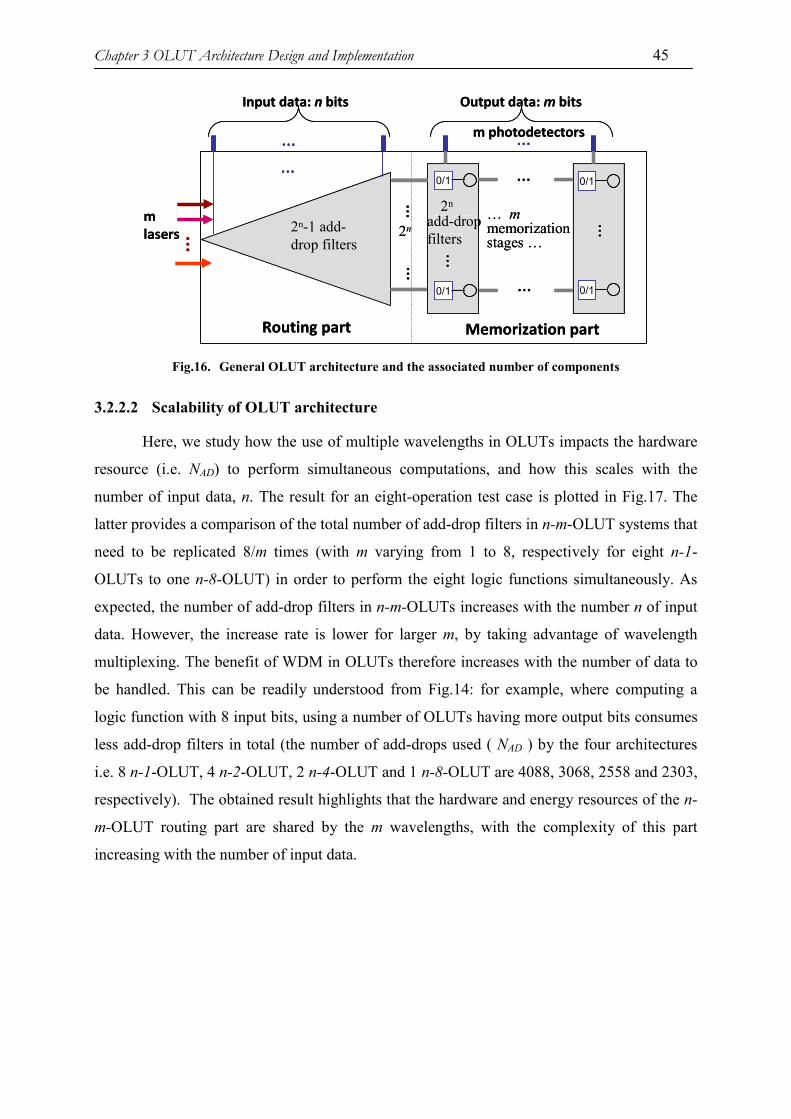
Chapter 3 OLUT Architecture Design and Implementation 45
2n
Routing part Memorization part
…
……
…0/1
… …
m lasers
… mmemorization stages …
…
…
… …
0/1
0/1
0/1
2n-1 add-drop filters
add-drop filters
m photodetectors
2n
Input data: n bits Output data: m bits
…
0/1
0/1
2n
Routing part Memorization part
…
0/1
0/1
aadd-drop drop filtersfilters
2n…
……
…0/10/1
… …
m lasers
… mmemorization stages …
…
…
… …
0/10/1
0/10/1
0/10/1
2n-1 add-drop filters
add-drop filters
m photodetectors
2n
Input data: n bits Output data: m bits
Fig.16. General OLUT architecture and the associated number of components
3.2.2.2 Scalability of OLUT architecture
Here, we study how the use of multiple wavelengths in OLUTs impacts the hardware
resource (i.e. NAD) to perform simultaneous computations, and how this scales with the
number of input data, n. The result for an eight-operation test case is plotted in Fig.17. The
latter provides a comparison of the total number of add-drop filters in n-m-OLUT systems that
need to be replicated 8/m times (with m varying from 1 to 8, respectively for eight n-1-
OLUTs to one n-8-OLUT) in order to perform the eight logic functions simultaneously. As
expected, the number of add-drop filters in n-m-OLUTs increases with the number n of input
data. However, the increase rate is lower for larger m, by taking advantage of wavelength
multiplexing. The benefit of WDM in OLUTs therefore increases with the number of data to
be handled. This can be readily understood from Fig.14: for example, where computing a
logic function with 8 input bits, using a number of OLUTs having more output bits consumes
less add-drop filters in total (the number of add-drops used ( NAD ) by the four architectures
i.e. 8 n-1-OLUT, 4 n-2-OLUT, 2 n-4-OLUT and 1 n-8-OLUT are 4088, 3068, 2558 and 2303,
respectively). The obtained result highlights that the hardware and energy resources of the n-
m-OLUT routing part are shared by the m wavelengths, with the complexity of this part
increasing with the number of input data.

Chapter 4 From architecture to device: multi-level modelling and simulation 67
(Fig.28). The thermo-optic effect can be obtained by simply applying an electric current to a
micro-heater integrated onto or inside the device region. As illustrated in Fig.29, it can be
realized by putting metallic resistors on top of the device claddings [146], or by heating the
silicon device through doped/silicided resistors [147], or by directly integrating the heater
inside the core of a silicon waveguide [148].
In OLUTs, the thermo-optic effect is typically needed to align the initial resonances of
the ring resonators with respect to the incoming signal wavelengths in a step referred to as a
“pre-calibration”. This would compensate for the fabrication inaccuracy of the microring, and
stabilize the initial OLUT configuration (i.e. configure the state of the add-drop filters in the
memorization part when the RAM value is applied). Some approaches are possible to reduce
the temperature drift, e.g. incorporating the cladding material with a temperature dependency
that is opposite to silicon [115]. However, they are not CMOS compatible at the current stage.
It is also possible to improve the temperature stabilization through the use of higher order
rings (i.e. cascading multiple rings), but the device complexity, footprint and power
consumption will be disadvantageously increased [164].
Fig.28. Microring resonator with integrated heater structure [154]
Waveguide coreBuried oxide
Silicon substrate
Silicon wireTop oxide cladding
Metal resistor
Heating current
Silicon waveguide
Waveguide coreBuried oxide
Silicon substrate
Silicon wireTop oxide cladding
Metal resistor
Heating current
Silicon waveguide
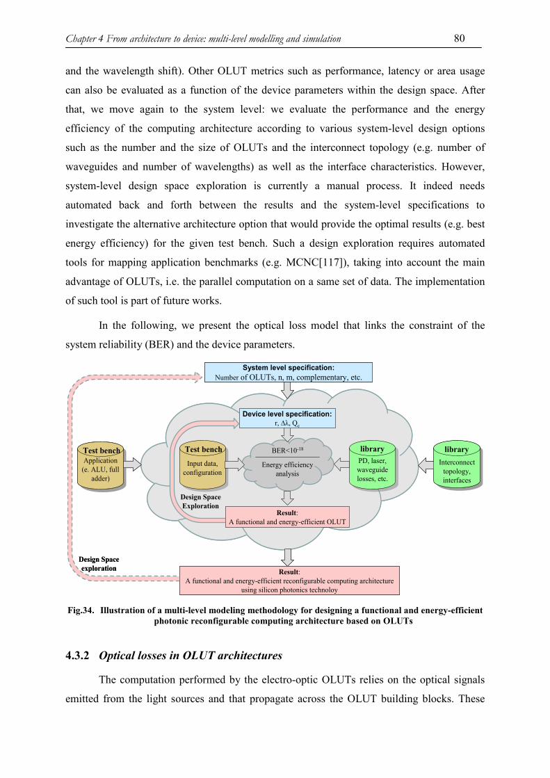
Chapter 4 From architecture to device: multi-level modelling and simulation 80
and the wavelength shift). Other OLUT metrics such as performance, latency or area usage
can also be evaluated as a function of the device parameters within the design space. After
that, we move again to the system level: we evaluate the performance and the energy
efficiency of the computing architecture according to various system-level design options
such as the number and the size of OLUTs and the interconnect topology (e.g. number of
waveguides and number of wavelengths) as well as the interface characteristics. However,
system-level design space exploration is currently a manual process. It indeed needs
automated back and forth between the results and the system-level specifications to
investigate the alternative architecture option that would provide the optimal results (e.g. best
energy efficiency) for the given test bench. Such a design exploration requires automated
tools for mapping application benchmarks (e.g. MCNC[117]), taking into account the main
advantage of OLUTs, i.e. the parallel computation on a same set of data. The implementation
of such tool is part of future works.
In the following, we present the optical loss model that links the constraint of the
system reliability (BER) and the device parameters.
Device level specification:r, ∆λ, Qc
System level specification:Number of OLUTs, n, m, complementary, etc.
Input data, configurationInput data,
configurationApplication (e. ALU, full
adder)
Application (e. ALU, full
adder)
PD, laser, waveguide losses, etc.
PD, laser, waveguide losses, etc.
Interconnect topology, interfaces
Interconnect topology, interfaces
Energy efficiency analysis
BER<10-18
Result:A functional and energy-efficient OLUT
Result:A functional and energy-efficient reconfigurable computing architecture
using silicon photonics technoloy
library libraryTest benchTest bench
Design Space Exploration
Design Space exploration
Device level specification:r, ∆λ, Qc
System level specification:Number of OLUTs, n, m, complementary, etc.
Input data, configuration
Input data, configurationInput data,
configurationApplication (e. ALU, full
adder)
Application (e. ALU, full
adder)
Test benchTest benchApplication Application Application Application
(e. ALU, full Application
(e. ALU, full (e. ALU, full (e. ALU, full (e. ALU, full (e. ALU, full adder
(e. ALU, full adder)
(e. ALU, full )adderadderadderadder)adder))
Application (e. ALU, full
adder)
PD, laser, waveguide losses, etc.
PD, laser, waveguide waveguide losses, etc.losses, etc.
PD, laser, waveguide losses, etc.
Interconnect topology, interfaces
Interconnect topology, interfaces
library
Interconnect Interconnect Interconnect Interconnect topology, topology, topology, topology,
interfacestopology,
interfacesinterfacesinterfacesinterfacesinterfaces
Interconnect topology, interfaces
Energy efficiency analysis
BER<10-18
Result:A functional and energy-efficient OLUT
Result:A functional and energy-efficient reconfigurable computing architecture
using silicon photonics technoloy
library libraryTest benchTest bench
Design Space Exploration
Design Space exploration
Fig.34. Illustration of a multi-level modeling methodology for designing a functional and energy-efficient photonic reconfigurable computing architecture based on OLUTs
4.3.2 Optical losses in OLUT architectures
The computation performed by the electro-optic OLUTs relies on the optical signals
emitted from the light sources and that propagate across the OLUT building blocks. These

Chapter 4 From architecture to device: multi-level modelling and simulation 84
upon adding some optical losses along the optical paths of the n-mx2-OLUT. We discuss the
contribution of the total energy for the n-m-OLUT in detail in the next section.
n
2n
Routing partMemorization part
…
……
…
0/1
m
… …
m lasers … m stages …
…
…
… …
0/1
0/1
0/1
nB: input data rate mB: output data rate
B: data rate (bit/s)
2n-1 add-drop filters
add-drop filters
- Dynamical energy: Ed- Static energy: Es
- Static energy: Es
- Elaser
- Epd
m photodetectors
2n
……
…
0/1
0/1
n
2n
Routing partMemorization part
…
0/1
0/1
aadd-drop drop filtersfilters
2n…
……
…
0/10/1
m
… …
m lasers … m stages …
…
…
… …
0/10/1
0/10/1
0/10/1
nB: input data rate mB: output data rate
B: data rate (bit/s)
2n-1 add-drop filters
add-drop filters
- Dynamical energy: Ed- Static energy: Es
- Static energy: Es
- Elaser
- Epd
m photodetectors
2n
n
2n
Routing part
Memorization part
…
……
…
0/1
m
… …
m lasers … m stages …
…
…
… …
0/1
0/1
0/1
nB: input data rate
B: data rate (bit/s)
2n-1 active add-drop filters
Active add-drop filters
- Dynamical energy: Ed /2- Static energy: Es /2 - Static energy: Es /2
- Elaser
- Epd
m photodetectors
2n
/omplementary part
……
m
…
… m stages …
…
…
…
2mB: output data rate
Passive add-drop filters
- Epd
m photodetectors
2n
………
…
0/1
0/1
n
2n
Routing part
Memorization part
…
0/1
0/1
Active Active aadd-drop drop filtersfilters…filters…
2n…
……
…
0/10/1
m
… …
m lasers … m stages …
…
…
… …
0/10/1
0/10/1
0/10/1
nB: input data rate
B: data rate (bit/s)
2n-1 active add-drop filters
Active add-drop filters
- Dynamical energy: Ed /2- Static energy: Es /2 - Static energy: Es /2
- Elaser
- Epd
m photodetectors
2n
/omplementary part
… ………
…
PPassive aadd-drop drop filtersfilters…filters…
2n
…m
…
… m stages …
…
…
…
2mB: output data rate
Passive add-drop filters
- Epd
m photodetectors
2n
…
Fig.36. Reminders of (a) the general architecture of n-m-OLUTs associated with all the terms of energy dissipations (b) the general architecture of n-mx2-OLUTs associated with all the terms of energy
dissipations
4.3.3.1 Dynamic Energy Ed
The OLUT dynamic energy dissipation Ed (energy-per-output-bit, in J/bit) relies on the
switching activity of the 2n-1 add-drop filters in the routing part and is given by
Ed= (2n-1) Esw/m (4.16)