
UNIVERSITÉ DE MONTRÉAL1 - publications.polymtl.ca · discrimination angulaire et le filtrage du...
134
UNIVERSITÉ DE MONTRÉAL ÉTUDE ET RÉALISATION DE MATRICES À COMMUTATION DE FAISCEAUX EN TECHNOLOGIE GUIDE D’ONDES INTEGRÉ AU SUBSTRAT TAREK DJERAFI DÉPARTEMENT DE GÉNIE ÉLECTRIQUE ÉCOLE POLYTECHNIQUE DE MONTRÉAL THÈSE PRÉSENTÉE EN VUE DE L’OBTENTION DU DIPLÔME DE DU DIPLÔME DE PHILOSOPHIE DOCTOR (Ph.D.) (GÉNIE ÉLECTRIQUE) AVRIL 2011 © Tarek Djerafi, 2011.
Transcript of UNIVERSITÉ DE MONTRÉAL1 - publications.polymtl.ca · discrimination angulaire et le filtrage du...
UNIVERSITÉ DE MONTRÉAL
ÉTUDE ET RÉALISATION DE MATRICES À COMMUTATION
DE FAISCEAUX EN TECHNOLOGIE
GUIDE D’ONDES INTEGRÉ AU SUBSTRAT
TAREK DJERAFI
DÉPARTEMENT DE GÉNIE ÉLECTRIQUE
ÉCOLE POLYTECHNIQUE DE MONTRÉAL
THÈSE PRÉSENTÉE EN VUE DE L’OBTENTION
DU DIPLÔME DE DU DIPLÔME DE PHILOSOPHIE DOCTOR (Ph.D.)
(GÉNIE ÉLECTRIQUE)
AVRIL 2011
© Tarek Djerafi, 2011.
UNIVERSITÉ DE MONTRÉAL
ÉCOLE POLYTECHNIQUE DE MONTRÉAL
Cette thèse intitulée:
ÉTUDE ET RÉALISATION DE MATRICES À COMMUTATION
DE FAISCEAUX EN TECHNOLOGIE
GUIDE D’ONDES INTEGRÉ AU SUBSTRAT
présenté par : DJERAFI Tarek
en vue de l’obtention du diplôme de : Philosophie Doctor (Ph.D.)
a été dûment accepté par le jury d’examen constitué de :
M. HACCOUN David, PH.D., président
M. WU Ke, Ph.D., membre et directeur de recherche
M. SERIOJA Tatu, Ph.D., membre
M. KOUKI Ammar, Ph.D., membre externe

iii
DÉDICACE
A mes parents,
A mes sœurs et frères,
Aux martyrs de la révolution Algérienne du 1 novembre 1954.
«Seul l'effort personnel enrichit et libère»

iv
REMERCIEMENTS
Je tiens à exprimer mes sincères remerciements à mon directeur de recherche, Monsieur Ke
Wu, professeur à l’École Polytechnique de Montréal, pour son support, ses conseils, son
enthousiasme et pour sa confiance.
Je tiens à remercier l’équipe de soutien du laboratoire. Merci à Traian Antonescu, Steve
Dubé, Jules Gauthier, Maxim Thibaut et Roch Brassard pour leurs conseils et leur disponibilité
lors de la fabrication des divers prototypes. Une grande partie des travaux de ce projet de doctorat
n’aurait pas été possible sans leur aide. Je crois qu’ils font aussi l’excellence de notre centre de
recherche.
Merci à Jean-Sébastien Decarie pour le soutien informatique, son dévouement, sa
disponibilité et surtout pour ses encouragements et son amitié.
Merci à Ginette Desparois et à Nathalie Lévesque pour leur dévouement envers les
étudiants du laboratoire.
Finalement, je tiens à remercier les membres de la communauté de Poly-GRAMES pour
leur camaraderie, les précieux moments de discussion et les dîners colorés. Merci mes amis.
v
RÉSUMÉ
Les applications radar pour les voitures demandent des composants de hautes performances
mais avec faible coût de revient. Cette thèse présente la conception des réseaux d’alimentation
d’antennes en ondes millimétriques utilisant la technologie du guide d’ondes intégré aux substrats
(GIS), pour satisfaire les exigences du coût et du faible encombrement dans ces applications de
radar.
Dans un système radar, l’antenne défini la largeur du secteur couvert, la portée, la
discrimination angulaire et le filtrage du bruit généré par d’autre sources. Généralement les
antennes intelligentes remplissent ce cahier des charges. La direction dans laquelle le réseau
ayant la réponse maximale serait la direction du pointage de faisceau. Pour un choix de faisceau
dans une direction désirée, un ajustement de phase doit être accompli. Les matrices à
commutation donnent des distributions de phase aux sorties différentes pour chaque port d’entrée.
Le guide d’ondes intégré aux substrats (GIS) offre une technologie intéressante pour les
réseaux d’alimentation d’antennes en termes de faible pertes par radiation, ce qui assure un très
faible niveau d’interférences et d’effets parasitiques entre les circuits de GIS. Nous proposons
dans ce travail plusieurs matrices de formation de faisceaux basées sur la technologie GIS. La
thèse est présentée sous forme d’articles.
Ce travail montre les étapes entreprises afin de mener à terme la conception, la fabrication,
les mesures et l’évaluation de plusieurs topologies de la matrice de Butler. Nous verrons donc
dans un premier temps les composants nécessaires au bon fonctionnement d’un tel système soit:
les coupleurs 3 dB, les déphaseurs et les croisements. Le choix de la configuration sera justifié
pour chacun de ces éléments. L’usage de simulateur (Ansoft HFSS) basé sur la méthode des
éléments finis (une méthode à ondes complètes) sera nécessaire dans ce travail. Ce logiciel donne
des résultats assez proches des essais expérimentaux. Trois matrices de Butler sont développées,
la première à 77 GHz sans croisement, une deuxième est une structure à deux couches à 24 GHz
et la troisième est une matrice complètement planaire avec un coupler 0 dB à 12.5 GHz.
On s’intéresse aussi à la matrice de Nolen; cette matrice offre par rapport à la matrice de
Butler l’avantage de ne pas présenter de croisement. Les charges disposées aux ports non utilisés
dans la matrice de Blass ne figurent pas dans la matrice de Nolen, ce qui augmente l’efficacité.

vi
On propose deux architectures, une en treillis dans la bande Ku et une deuxième en parallèle qui
affiche de bonnes performances sur une large bande autour de 77 GHz.
Le niveau des lobes latéraux (SLL – Side Lobe Level) augmente avec l’angle de pointage
des réseaux d’antennes. Cette caractéristique affecte l’efficacité des matrices de Butler puisque la
diminution des interférences est en fonction du niveau du SLL. Une architecture basée sur des
coupleurs variables est proposée pour contrôler le SLL. Ce coupleur variable est fabriqué avec un
guide d’ondes métallique WR28. Les résultats de mesures sont utilisés pour estimer les
performances de la matrice de Butler en termes de SLL.
Une architecture basée sur le concept de réseaux adaptatifs est proposée pour le radar long
distance à 77GHz en diminuant le nombre des déphaseurs variables. Un réseau primaire alimenté
(sous-réseaux) par des réseaux secondaires qui doivent satisfaire une contrainte de
chevauchement.
Les conclusions de ces travaux et les suggestions pour les travaux futurs seront présentées
dans le dernier chapitre de cette thèse.
Ces travaux sont une première investigation entrepris dans notre groupe de recherche afin
de maîtriser les différentes matrices et de définir les contraintes additionnelles dans l’utilisation
du GIS. Nous espérons que l’ensemble des informations regroupées dans ce rapport de thèse sera
particulièrement utile dans la conception d’un système d’aide à la conduite fiable, léger et faible
coût.

vii
ABSTRACT
Automotive radar applications require components with high performance but low cost.
This thesis presents the design of millimeter wave antennas feeding networks using the substrate
integrated waveguide (SIW) technology, to satisfy the requirement of low cost and compactness
in these radar applications.
In a radar system the antenna define the width of covered area, the range, the angular
discrimination and the filter noise generated by other sources. Generally smart antennas must be
used to satisfy the specifications. The beam pointing can be achieved only by adjusting the phase
of signals from different elements. For a choice of beam in a desired direction, a phase
adjustment must be done. Switching matrices are used to provide phase distribution at output
ports that is different for each input port.
The substrates integrated waveguide (SIW) is a promising technology for the antenna feed
networks in terms of low radiation and transmission losses with reduced interferences among
SIW circuit elements. We propose in this work several beamforming matrices based on SIW
technology. This thesis is presented in paper form.
First of all, this work shows the steps taken to finalize the design, fabricate, measurement
and evaluation of several Butler matrix topologies. We will see at first that the building
components necessary for the proper functioning of such a network: the 3 dB couplers, phase
shifters and crossovers. The choice of a configuration will be justified for each of these elements.
An electromagnetic simulator (Ansoft HFSS) based on the finite element method (full-wave
method) is used in this work. This software package would be able to yield results close to
experimental counterparts. Three Butler matrices are developed, the first at 77GHz without
crossover, the second is related to a two layer structure at 24 GHz and the third is completely
made planar with a cross-over at 12.5 GHz.
The Nolen matrix compared to Butler matrix has the advantages of being free from
crossovers in the structure. The loads placed on unused ports in the Blass matrix do not appear in
the Nolen matrix which increases efficiency. We propose two architectures, the first one is
related to perpendicular configuration in Ku band while the second platform presents a parallel
topology which shows a good performance over a broad band around 77 GHz.

viii
In the design of antenna systems, the sidelobe level (SLL) should be taken care of in a
special manner, which generally increases with the pointing angle of antenna arrays. This
characteristic affects the efficiency of Butler matrices since the reduction of interference is based
on the level of SLL. An architecture based on variable couplers is proposed in this work to
control the SLL. This variable coupler is fabricated with a metallic waveguide WR28 and
measurement results are used to estimate the performance of the Butler matrix in terms of SLL.
In addition, an architecture based on the concept of adaptive networks is proposed for long
range radar systems at 77GHz. In this architecture, the number of variable phase shifters is
decreased. A primary network feeds secondary networks which must satisfy an overlapping
condition.
This thesis work will be concluded and also make recommendations for future work, which
are presented in the last chapter of this thesis.
This work is a first investigation commenced in our research group to control the various
beamforming matrices and to define the additional constraints in the use of GIS. We hope that all
the information gathered in this thesis report will be particularly useful in designing reliable,
lightweight and low cost radar system for automotive application.

ix
TABLE DES MATIÈRES
DÉDICACE ................................................................................................................................... III
REMERCIEMENTS ..................................................................................................................... IV
RÉSUMÉ ........................................................................................................................................ V
ABSTRACT .................................................................................................................................VII
TABLE DES MATIÈRES ............................................................................................................ IX
LISTE DES FIGURES .................................................................................................................XII
LISTE DES SIGLES ET ABRÉVIATIONS ............................................................................. XIV
LISTE DES ANNEXES ............................................................................................................. XVI
INTRODUCTION ........................................................................................................................... 1
1. CONSIDERATIONS GÉNÉRALES SUR LES RADARS .................................................... 5
1.1 Généralités ........................................................................................................................ 5
1.2 Fréquences utilisées .......................................................................................................... 7
1.3 L’effet des pertes par radiation dans les réseaux en microruban ..................................... 8
1.4 Le GIS .............................................................................................................................. 9
1.4.1 Structure du GIS ......................................................................................................... 10
1.4.2 Les GIS dans la littérature .......................................................................................... 11
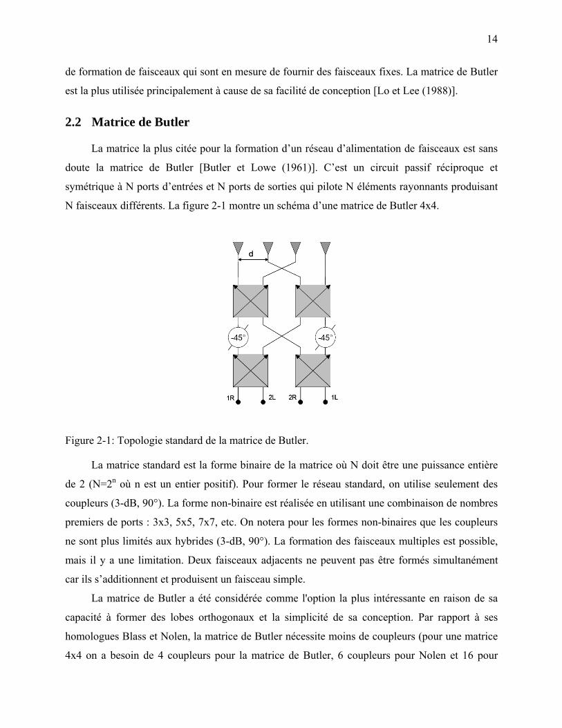
2 MATRICE DE BUTLER ...................................................................................................... 13
2.1 Antenne intelligente ....................................................................................................... 13
2.2 Matrice de Butler ............................................................................................................ 14
2.3 Matrice de Butler 2x2 ..................................................................................................... 15
2.4 Matrices de Butler dans la littérature ............................................................................. 17
2.5 Matrice de Butler planaire sans croisement (Annexe I) ................................................. 20
2.6 Matrice de Butler en deux couches (Annexe II) ............................................................ 21

x
2.7 Matrice de Butler planaire avec croisements (Annexe III) ............................................ 22
3. MATRICE DE BLASS ET NOLEN ..................................................................................... 24
3.1 Matrice de Blass ............................................................................................................. 24
3.2 Matrice de Nolen ............................................................................................................ 25
3.3 Largeur de bande ............................................................................................................ 27
3.4 Matrice de Nolen en treillis (Annexe IV) ....................................................................... 28
3.5 Matrice de Nolen large bande (Annexe V) .................................................................... 29
4. MATRICE DE BUTLER AVEC UN NIVEAU DE LOBES LATERAUX CONTROLÉ .. 30
4.1 Matrice de Butler avec un bas SLL basé sur l’augmentation du nombre de ports de
sortie …………………………………………………………………………………………30
4.2 Matrice de Butler avec un bas SLL basé sur l’utilisation d’atténuateurs ....................... 31
4.3 Matrice de Butler avec un Niveau de lobes lateraux controlé avec des coupleurs
variable (Annexe VI) .................................................................................................................. 33
5. ANTENNE POUR RADAR LONGUE DISTANCE À 77 GHZ ......................................... 34
5.1 Introduction .................................................................................................................... 34
5.2 Condition de chevauchement ......................................................................................... 35
5.3 Modes d’alimentation ..................................................................................................... 37
5.3.1 Réseaux d’alimentation avec recombinaison (Annexe VII) ...................................... 37
5.3.2 Réseaux d’alimentation en série (Annexe VIII) ......................................................... 38
5.3.3 Coupleur 0dB ............................................................................................................. 38
5.4 Conception de l’antenne ................................................................................................. 38
6. DISCUSSION GENERALE ................................................................................................. 42
CONCLUSIONS ET TRAVAUX FUTURS ................................................................................ 44
ANNEXES .................................................................................................................................... 54

xi
LISTE DES TABLEAUX
Tableau 2-1: Comparaison entre les différentes technologies........................................................ 19
Tableau 3-1: Paramètres de la Matrice de Nolen 4X4 retenue (θijφij) ............................................ 26

xii
LISTE DES FIGURES
Figure 1-1: Les différentes applications des radars automobiles. .................................................... 6
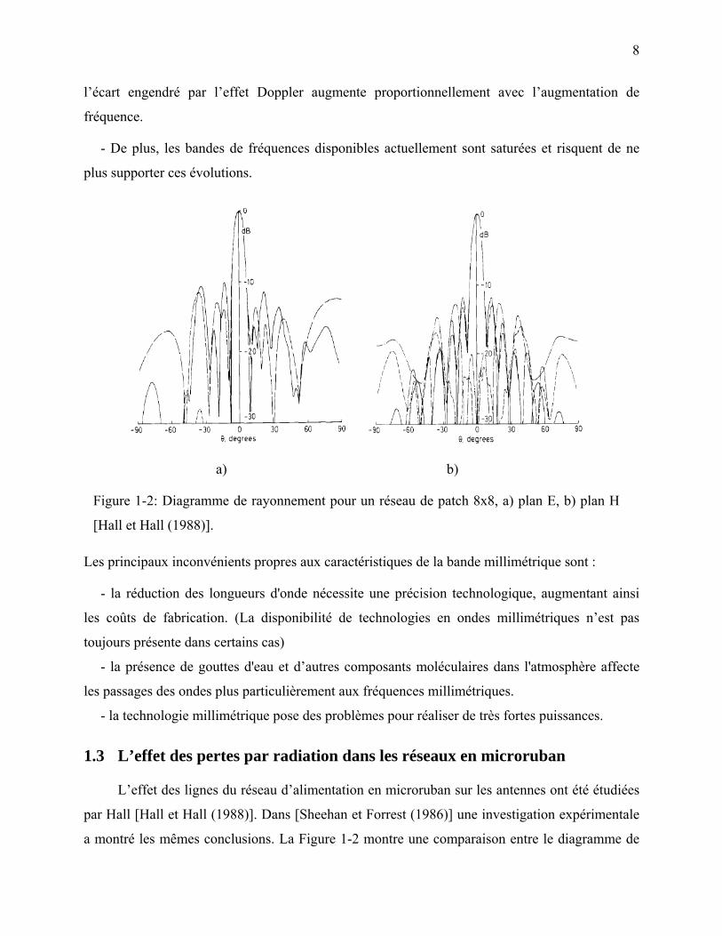
Figure 1-2: Diagramme de rayonnement pour un réseau de patch 8x8, a) plan E, b) plan H [Hall
et Hall (1988)]. ................................................................................................................................. 8
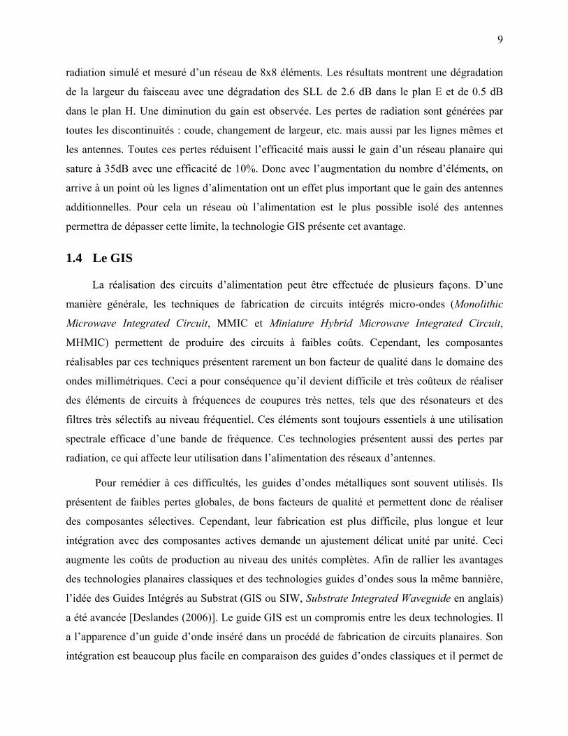
Figure 1-3: Guides équivalents avec indication de largeur équivalente. ........................................ 10
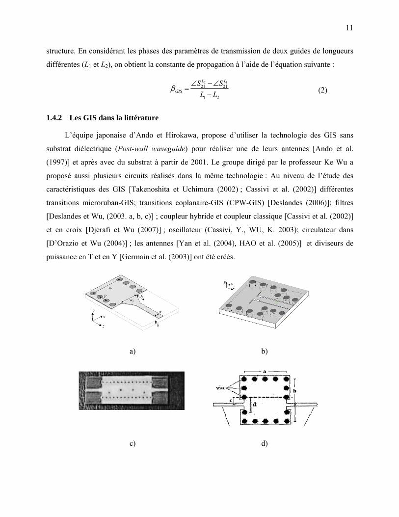
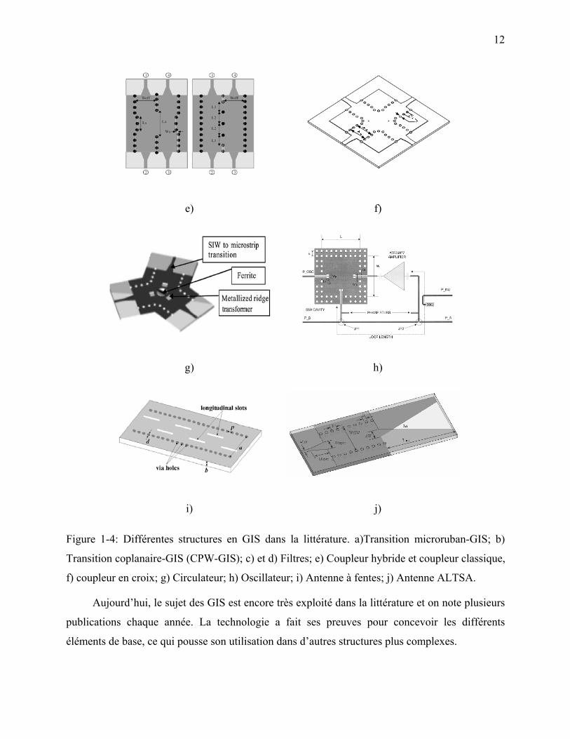
Figure 1-4: Différentes structures en GIS dans la littérature. a)Transition microruban-GIS; b)
Transition coplanaire-GIS (CPW-GIS); c) et d) Filtres; e) Coupleur hybride et coupleur classique,
f) coupleur en croix; g) Circulateur; h) Oscillateur; i) Antenne à fentes; j) Antenne ALTSA. ..... 12
Figure 2-1: Topologie standard de la matrice de Butler. ................................................................ 14
Figure 2-2: Matrice de Butler 2x2 (coupleur 3 dB) ....................................................................... 16
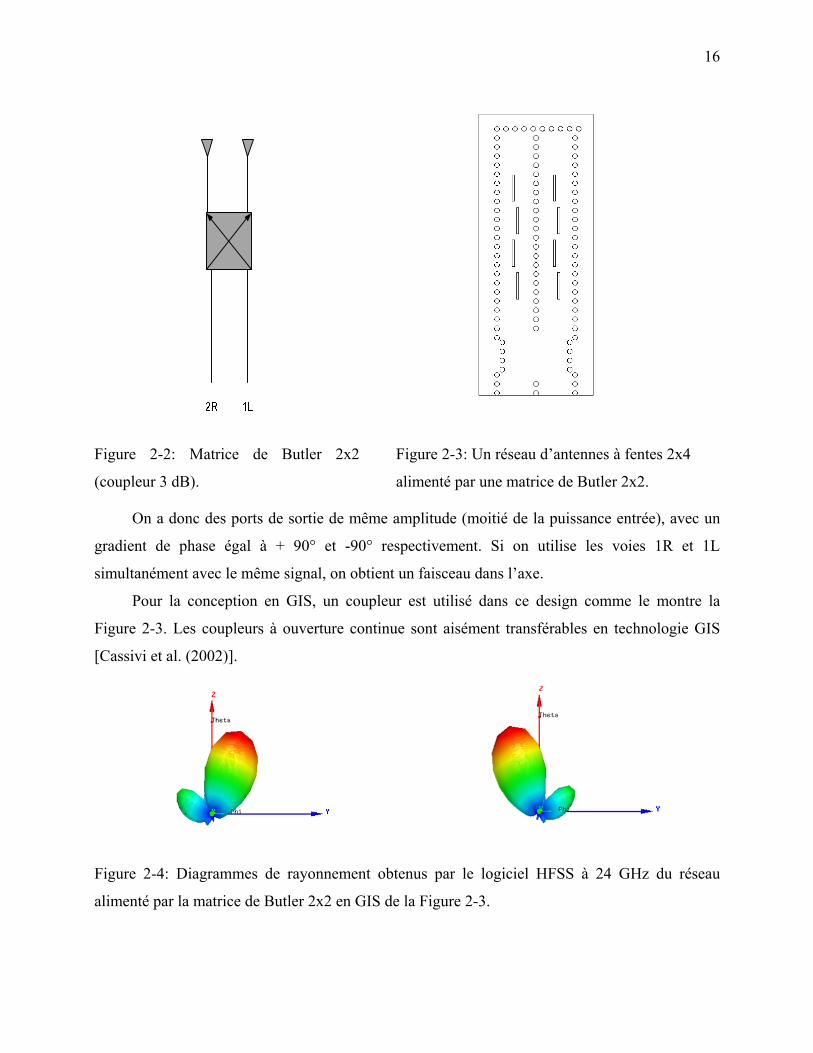
Figure 2-3: Un réseau d’antennes à fentes 2x4 alimenté par une matrice de Butler 2x2. .............. 16
Figure 2-4: Diagrammes de rayonnement obtenus par le logiciel HFSS à 24 GHz du réseau
alimenté par la matrice de Butler 2x2 en GIS de la Figure 2-3. ..................................................... 16
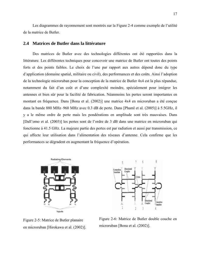
Figure 2-5: Matrice de Butler planaire en microruban [Hirokawa et al. (2002)] ........................... 17
Figure 2-6: Matrice de Butler double couche en microruban [Bona et al. (2002)] ........................ 17
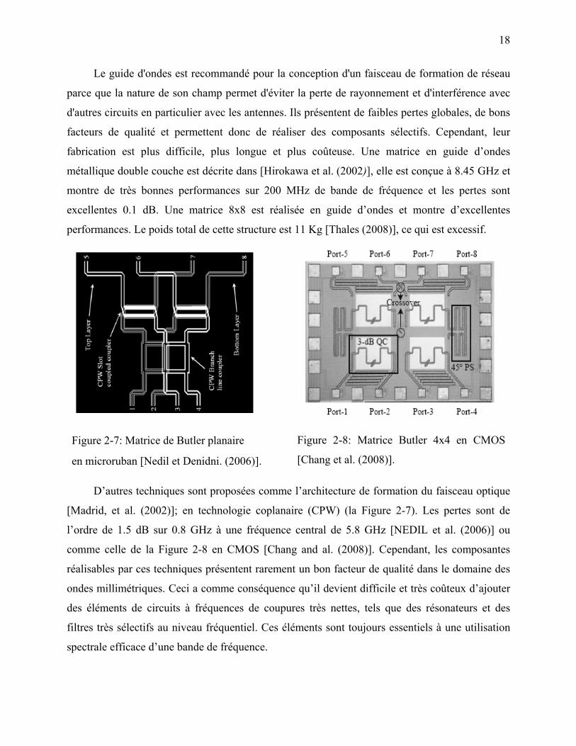
Figure 2-7: Matrice de Butler planaire en microruban [Nedil et Denidni. (2006)]. ....................... 18
Figure 2-8: Matrice Butler 4x4 en CMOS [Chang et al. (2008)]. .................................................. 18
Figure 2-9: Matrice de Butler par Yamamoto & Al. [Yamamoto et al. (2003)]. ........................... 19
Figure 2-10: Nouvelle topologie de la matrice de Butler 4x4. ....................................................... 20
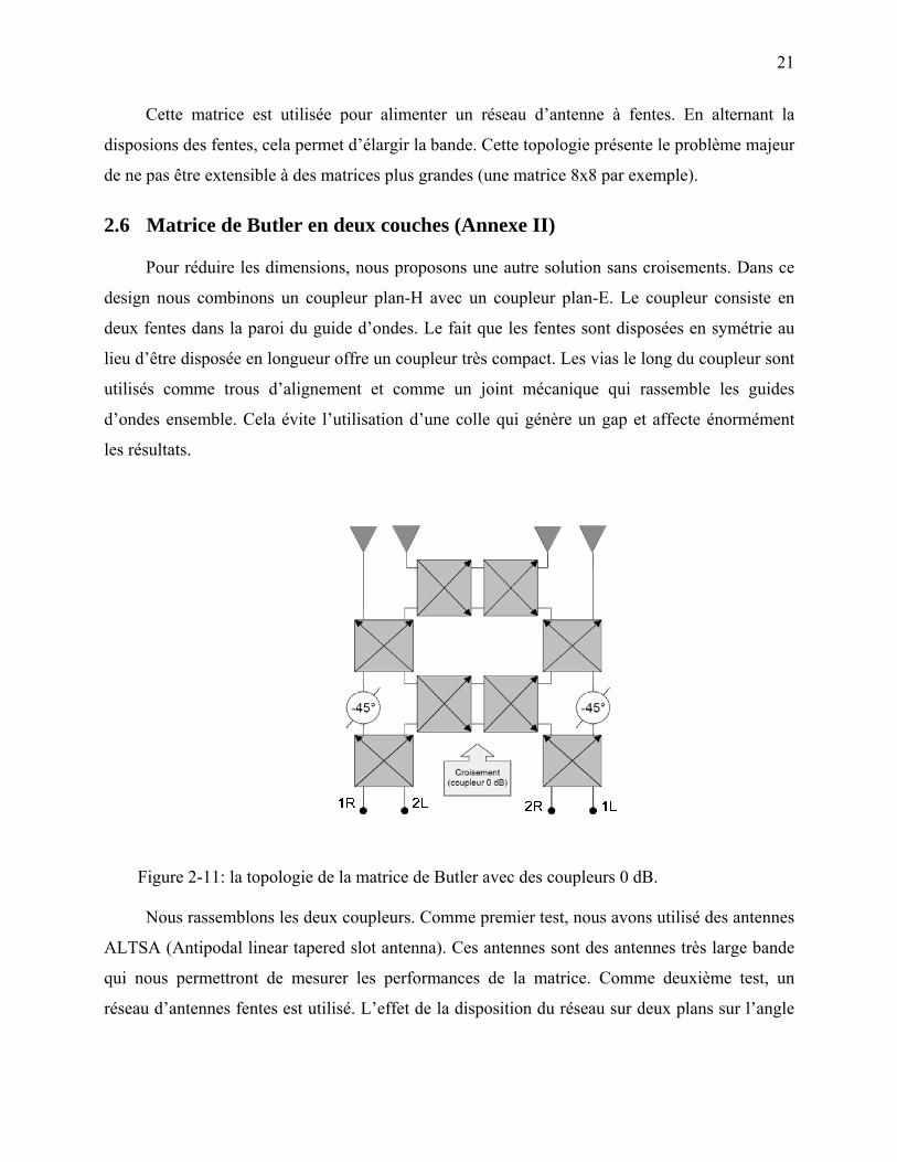
Figure 2-11: la topologie de la matrice de Butler avec des coupleurs 0 dB ................................... 21
Figure 3-1: Topologie de la Matrice de Blass. ............................................................................... 25
Figure 3-2: Forme générale d’une matrice de Nolen et détail d’un nœud de la matrice. ............... 26
Figure 4-1: Réseau de huit antennes alimentées par une Matrice de Butler 4x8. .......................... 31
Figure 4-2: Diagramme de rayonnement d’un réseau de 8 antennes patch alimentées par la
matrice de Butler4x8 avec une distribution binominale. ................................................................ 31

xiii
Figure 4-3: Matrice de Butler 4x4 avec des atténuateurs ............................................................... 32
Figure 4-4: Diagramme de rayonnement d’un réseau de 4 antennes patch alimentées par la
matrice de Butler 4x4 avec une distribution binominal. ................................................................ 32
Figure 4-5: Matrice de Butler 4x4 modifiée. (a) les valeurs des couplages quand le port1 et le
port2 sont utilisées (b) les valeurs des couplages quand le port3 et le port4 sont utilisées ............ 33
Figure 5-1: Réseau d’antennes avec des sous réseaux identiques. ................................................. 34
Figure 5-2: Facteur du réseau d’antennes basé sur le concept des sous réseaux ........................... 35
Figure 5-3: Distributeur binominal ................................................................................................ 38
Figure 5-4: Réseau de cinq antennes Yagi alimentées par un distributeur non uniforme en phase
(0 degré). ........................................................................................................................................ 39
Figure 5-5: Réseau d’alimentation de 20 antennes alimentées par des réseaux chevauchés 4x5
avec des coefficients d’excitation (1 :1.71 :1.71 :1) et un gradient de phase (90 degrés).............. 39
Figure 5-5: Diagramme de rayonnement d’un réseau de 20 antennes patch alimentées par un
réseau chevauché 4x5 avec des coefficients d’excitation (1 :1.71 :1.71 :1) et un gradient de phase
(0 degré). ........................................................................................................................................ 40
Figure 5-6: Diagramme de rayonnement d’un réseau de 20 antennes alimentées par des réseaux
chevauchés 4x5 avec des coefficients d’excitation (1 :1.71 :1.71 :1) et un gradient de phase (90
degrés). ........................................................................................................................................... 40

xiv
LISTE DES SIGLES ET ABRÉVIATIONS
aeq Largeur de guide d’ondes rectangulaire équivalente
βGIS La constante de propagation d’un guide GIS.
C Nombre des croisements dans une matrice de Butler
c La vitesse de la lumière dans le vide.
d La différence de phase chaque deux éléments adjacents pour réaliser
θΔ Variation dans la direction du pointage (l’angle de balayage)
ε La permittivité électrique
εr La permittivité relative
δϕ Déviation de la phase
f La fréquence
H Nombre des coupleurs dans une matrice de Butler
λo La longueur d'onde en espace libre
µ La perméabilité magnétique
N Éléments un réseau séparé de
P Nombre déphaseurs fixes dans une matrice de Butler
θ L’angle du pointage
ω La fréquence angulaire
ABS Anti-Lock Braking System
ACC Adaptive Cruise Control
ADS Advanced Design System
AICC Autonomous Intelligent Cruise Control
ALTSA Antipodal Linear Tapered Slot Antenna
BFN Beamforming network

xv
CAC Contrôle automatique de la croisière
CC Condition de Chevauchement
ESB Electronic Stability Braking
FLR Forward Loking Radar
FM/CW Frequency Modulated Continuous Wave
GIS Guide Integré au Substrat
HFSS High Frequency Structure Simulator
IEEE the Institute of Electrical and Electronics Engineers
LMR Ligne Microruban
LRR Long Range Radar
RADAR Radio Detection and Ranging
RWG Rectangular Waveguide
SIW Substrate Integrated Waveguide
S/N Signal to Noise Ratio
SLL Side Lobes Level
SRR Short Range Radar

xvi
LISTE DES ANNEXES
Article I: A Low-Cost Wideband 77-Ghz Planar Butler Matrix In Siw Technology ................... 55
Article II: Multi-Layered Substrate Integrated Waveguide Butler Matrix For Millimeter-Wave
System Applications ...................................................................................................................... 62
Article III: Design And Implementation Of A Planar 4×4 Butler Matrix In Siw Technology For
Wide Band High Power Applications ........................................................................................... 74
Article IV: Planar Ku-Band 4x4 Nolen Matrix In Siw Technology ............................................. 84
Article V: Broadband Substrate Integrated Waveguide Nolen Matrix Based On Coupler Delay
Compensation ................................................................................................................................ 93
Article VI: Variable Coupler For Low Side Lobe Level Butler Matrix .......................................100
Article VII: 77 Ghz Recombinant Substrate Integrated Waveguide Power Divider .................. 108
Article VIII: Corrugated Substrate Integrated Waveguide (Siw) Antipodal Linearly Tapered Slot
Antenna Array Feed By Quasi-Triangular Power Divider .......................................................... 112

1
INTRODUCTION
Dans des applications de télécommunication et radar, on a besoin de couvrir un grand
secteur autour de la station interrogatrice. Ce type de transmission a pour conséquence de polluer
l’environnement électromagnétique en rayonnant de la puissance dans des directions inutiles.
Une solution à ce problème est de générer plusieurs faisceaux dans des directions fixes ou
mobiles et avec un commutateur balayer tout le secteur désiré. Les antennes intelligentes sont
basées sur des réseaux d’antennes (linéaire, planaire, circulaire...). Ces antennes peuvent être
orientées dans des directions privilégiées pour suivre une cible mobile afin de réduire les niveaux
des signaux brouilleurs émis par d’autres mobiles. L’opération est effectuée grâce aux antennes
réseaux et à des techniques de traitement du signal dédiées (calcul d’angle d’arrivée, de
pondérations d’amplitude, de pondération de phase, etc.) qui permettent à l’antenne de se
focaliser sur un utilisateur donné tout en minimisant l’impact des trajets multiples, du bruit et des
interférences qui sont responsables de la dégradation de la qualité des signaux. Généralement des
matrices (comme la matrice de Butler) sont utilisées dans l’alimentation des antennes
intelligentes avec un réseau à faisceau commutable.
Dans les réseaux d’alimentation de faisceaux (Beamforming Network en anglais) afin de
former les faisceaux multiples, un choix de N éléments d’antenne est relié à M ports des
faisceaux. Un résultat simple de réseau est formé quand des signaux induits sur différents
éléments de réseau sont combinés. La direction où le réseau possède la réponse maximale sera la
direction du pointage de faisceau. L’orientation de faisceau conventionnel peut être réalisée en
ajustant seulement la phase des signaux des différents éléments. Pour diriger le faisceau dans une
direction désirée, une distribution de phase doit être accomplie. Plusieurs techniques existent et
fournissent ces faisceaux fixes. Les matrices de Butler et de Blass, par exemple, sont souvent
employées.
Une technologie qui permet de réduire significativement les coûts de production est le
Guide Intégré au Substrat (GIS). Ce guide construit directement sur un substrat planaire confine
le champ électromagnétique à l’aide de deux rangées de cylindres métalliques ou fentes
métallisées. Le GIS permet de concevoir tous les composants passifs et d’assembler tous les
composants actifs sur un même support. Le GIS présente l’avantage de ne pas avoir des pertes
2
par radiation avec des pertes de transmission réduites et en conséquence ne pas affecter le
rayonnement des antennes associées.
L’objectif du travail est la conception, la fabrication et la mesure des différentes matrices à
commutation de faisceau en technologie GIS pour les applications à 24GHz, pour le radar à
77GHz, et d’explorer un réseau d’antenne adaptative. En effet, les radars à basse de fréquences
10GHz ou 24GHz sont utilisés pour couvrir une ou plusieurs larges sections, le radar à 77GHz
couvre un petit secteur mais nécessite un grand gain. La thèse est présentée sous forme d’articles.
Dans le premier chapitre, une description des radars d’aide à la conduite automobile, leurs
historiques et leurs applications sont détaillées. Les caractéristiques des antennes utilisées sont
critiques pour les performances de ces systèmes. Les pertes dans les réseaux d’alimentation
d’antennes fabriqués en technologie microruban affectent les patrons de radiation de ces
antennes, spécialement au niveau des lobes latéraux. La solution en guide d’ondes métallique
reste l’idéal en termes de perte mais représente un poids et un coût élevés. Nous proposant
d’utiliser le GIS qui représente un compromis entre les deux technologies. Les concepts de base
des GIS seront présentés.
Le deuxième chapitre, s’intéresse aux matrices de Butler et ces différentes topologies. La
première matrice est une matrice complètement planaire composée de quatre coupleurs et de deux
déphaseurs sans utiliser les croisements. Cette matrice est réalisée à 77GHz et est utilisée pour
alimenter un réseau d’antenne à fentes. La deuxième matrice est disposée sur deux couches. Le
changement d’une couche à une autre se fait à l’aide d’un coupleur plan-E. Cette matrice
compacte est utilisée pour alimenter des antennes des antennes à rayonnement longitudinal
(endfire en anglais), ces antenne affichent des performances sur une large bande et n’affectent pas
les performances de la matrice. Un réseau d’antennes à fentes est utilisé pour vérifier l’effet du
décalage engendré par l’épaisseur du substrat sur une radiation transversale (Broadside). Une
matrice de Butler 4x4 planaire où les croisements sont remplacés par deux coupleurs cascadés est
réalisée à la fréquence de travail de 12.5GHz. Un des objectifs est de concevoir la matrice pour
très large bande. Pour cela une amélioration sur un coupleur en croix est réalisée ainsi qu’un
croisement basé sur ce coupleur. Combiné à des déphaseurs, cette matrice montre des
performances sur une très large bande comparable à celles réalisées en microruban.
3
Le troisième chapitre propose deux matrices de Nolen en GIS. Ces matrices sont des
réseaux d’alimentation en série. La première matrice est réalisée en bande Ku. La conception, la
construction et les performances des différents éléments de ce design sont présentées. Les
différents éléments seront assemblés afin de construire la matrice qui sera réalisée et mesurée.
Les différentes performances seront discutées notamment la variation des différences de phase
avec la fréquence et son effet sur la direction du patron de radiation. La deuxième matrice
présente une excellente stabilité des distributions en amplitude et en phase sur une large bande.
Cette matrice possède la même largeur de bande que les matrices de Butler; elle permet de
réaliser des matrices avec un nombre de ports d’entrée différent de celui de ports de sortie.
Une matrice de Butler avec un niveau de lobes latéraux contrôlés est proposée dans le
quatrième chapitre. Cette matrice est basée sur un nouveau concept des coupleurs variables. La
matrice proposée, comparée aux autres méthodes de réduction des SLL, ne représente pas de
perte additionnelle et peut très bien générer différents SLL.
La faisabilité d’une antenne adaptative à 77GHz est étudiée dans le cinquième chapitre. Un
réseau qui peut balayer un petit angle avec moins de déphaseurs a été proposé. Un critère de
chevauchement doit être satisfait entre plusieurs sous-réseaux identiques. Pour cela, deux types
de diviseur ont été proposés ainsi qu’un croisement compact. Les résultats de simulation sont
présentés.
Cette thèse présente huit articles annexés. Le deuxième chapitre contient trois articles
soumis dans IEEE Transaction on Antennas & Propagation. Dans le troisième chapitre les deux
articles sur les matrices de Nolen ont été acceptés dans IEEE MTT-S Transaction. Idem pour
l’article qui couvre quatrième chapitre. Dans le chapitre cinq, deux type de diviseur sont proposés
comme parties de l’antenne. Le premier article « Corrugated Substrate Integrated Waveguide
(SIW) Antipodal Linearly Tapered Slot Antenna Array Feed by Quasi-Triangular Power
Divider » est soumis dans Transaction on Antennas & Propagation, les révisions ont été
envoyées. L’article « 77 GHz Recombinant Substrate Integrated Waveguide Power Divider»
soumis comme lettre pour letter on Antennas & Propagation.
Ces revues ont été choisies car elles sont reconnues mondialement et font office de
référence dans le domaine des antennes et des circuits passifs micro-ondes. La rédaction des
articles à fait l’objet d’un soin poussé afin de répondre aux contraintes de rigueur et d’analyse

4
demandées par les revues prestigieuses et par cette thèse de doctorat. Les articles sont insérés
comme annexes dans leur forme originale à la soumission.
Les principales contributions apportées par cette thèse sont les suivantes :
- Plusieurs composants passifs ont été proposés ou adaptés en technologie GIS :
- Un coupleur en croix avec une version large bande.
- Un coupleur en croix basé sur un miroir dans la région commune a été réalisé en GIS, ce
coupleur est une classe à part. Une nouvelle version a été conçue pour pouvoir générer des
couplages variables.
- Un diviseur qui génère une distribution binominale en recombinant la division après
chaque étage.
- Différentes matrices ont été adaptées en technologie GIS :
- Une matrice sans croisement a été utilisée pour alimenter un réseau de fentes alternées,
ce qui a formé une antenne large bande.
- Une matrice très large bande (25 %) a été réalisée. Cela démontre bien que le GIS peut
être utilisé pour concevoir des composants large bande, et même plus large bande que les
matrices en microruban.
- Une matrice de Nolen a été réalisée grâce a des coupleurs en croix, c’est la première
matrice réalisée en GIS autre que les matrices de Butler.
- La première matrice de Nolen large bande toutes technologies comprises a été proposée.
Le même concept est utilisable pour des matrices de Blass.
- Une nouvelle architecture d’une matrice de Butler avec un niveau de lobes latéraux bas est
proposée.
5
CHAPITRE 1
1. CONSIDERATIONS GÉNÉRALES SUR LES RADARS
1.1 Généralités
L’aide à la conduite se définit comme un ensemble de systèmes de sécurité actif,
d’information ou d’assistance au conducteur pour éviter l’apparition d’une situation dangereuse
pouvant aboutir à un accident. On peut citer entre autre la direction assistée, le système
antiblocage des roues (Anti-Lock Braking System en anglais (ABS)), le système du contrôle de
trajectoire (Electronic Stability Braking en anglais (ESP)) et également les systèmes radars qui
sont utilisés pour la prévention des collisions et pour assister le conducteur en automatisant
partiellement la conduite (par exemple, le maintien de la distance minimale entre deux véhicules).
Plus généralement, les radars d’aide à la conduite ont pour but principal de déterminer la distance
et la vitesse d’un obstacle et d’avertir le conducteur ou d’interagir avec les dispositifs de freinage
et de sécurité, tels que les coussins de sécurité gonflables.
Les systèmes radars pour voitures ont été étudiés par la majorité des grandes compagnies
automobiles et des instituts et des laboratoires de recherche depuis le début des années 70. Les
progrès rapides des technologies RF et l’arrivée des cartes DSP de plus en plus rapides ainsi que
la baisse des prix des composants en ondes millimétriques ces dernières années, ont rendu le
système radar de plus en plus intéressant comme un produit de consommation. Le domaine est en
train de passer rapidement du statut de recherche et développement à la phase de pré-production.
Il est attendu que les deux radars 24 GHz et 77 GHz deviennent de plus en plus communs dans
des véhicules personnels et aussi commerciaux.
Ces systèmes ont été développés d'abord à 10 GHz [Hahn (1995)], puis passés à des
fréquences plus élevées (34 et 50 GHz) [Jones et Grimes (1975); Linder et Wiesbeck (1976) et
Neininger (1977)] dans le milieu des années 1970 et à 60, 77 et 94 GHz dans les années 1990
[Groll et Detlefsen (1997)]. Les fréquences utilisées pour la plupart des systèmes radars
automobile dans le présent sont de 24 et 77 GHz. Les systèmes radars à courte et à longue
distance représentent un marché d'environ 11 millions et 2.5 millions d'unités par an [Hung
(2005)] respectivement.
6
Le radar 77 GHz est adapté jusqu'à 200 m, en raison de la possibilité de concevoir des
antennes avec un gain plus élevé qu’une antenne 24GHz dans le même package physique. Pour
courte portée (jusqu'à 50m), le radar 24 GHz doit être peu coûteux car de nombreux capteurs
doivent être placés sur une même voiture.
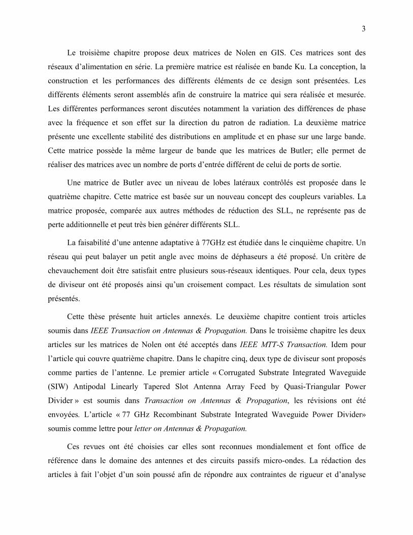
Il y a plusieurs applications pour les systèmes radars automobile comme indiqué sur la
figure 1-1. Pour le système 77 GHz; le système radar est utilisé comme: radar de prospection
(FLR), régulateur de vitesse et d'espacement (ACC), système d’alerte de changements de voie et
alerte aux obstacles. À l'avenir, il sera également utilisé comme système de conduite intelligent
(AICC). Le radar à 24 GHz peut assister le conducteur dans le stationnement, il pourra libérer les
coussins gonflables avant un impact réel, dans les embouteillages, dans le changement de voie ou
comme indicateur de vitesse et pour reconnaissance de l’état de la route.
Figure 1-1: Les différentes applications des radars automobiles.
Les systèmes radar pour les applications automobiles, autres que les applications militaires
ou celles de la recherche, reposent sur la demande des consommateurs. Cela inclut non seulement
des bonnes performances, mais aussi l’importance des critères économiques. Cela comprend le
coût de la production ainsi que les possibilités d'intégration dans un véhicule. Pour devenir la
norme dans la plupart des équipements automobiles, leur taille doit être suffisamment petite pour
être facilement intégrable dans les différentes parties d'une voiture et leur coût doit être diminué
de façon substantielle. Le coût d’installation d’un seul de ces deux radars est déjà assez élevé
7
(1500 USD - 3000 USD) ce qui constitue une contrainte majeure couplée à un problème de poids
et d’encombrement.
Il est intéressant de développer une seule plate-forme qui rassemble les deux systèmes 24
GHz et 77 GHz au lieu de les concevoir séparément. Le développement de cette plate-forme
permettra d’alléger le poids, diminuer la consommation DC, diminuer l’encombrement, etc. Nous
nous sommes fixés comme objectif le développement d’antennes séparément avant l’intégration
finale.
Une technologie qui permettra de réduire significativement les coûts de production est le
GIS. Celui-ci permet de concevoir tous les composants passifs et d’assembler tous les
composants actifs sur un même support. Un travail dans ce sens a été effectué au PolyGrames
notamment par Deslandes [Deslandes (2006)] et Cassivi [Cassivi (2004)].
1.2 Fréquences utilisées
Historiquement les ondes millimétriques (30 - 300 GHz) étaient surtout utilisées pour les
applications militaires comme les radars et l’imagerie, ainsi pour le domaine scientifique comme
pour la radio astronomie ou la télédétection. Il y a plusieurs raisons qui rendent des ondes
millimétriques attrayantes :
- La taille des antennes proportionnelle à la longueur d’onde est plus petite en montant en
fréquence.
- Une fréquence d'exploitation plus élevée entraîne aussi des antennes à gain plus élevé
puisque le gain augmente proportionnellement avec carré de la fréquence de fonctionnement.
Pour les systèmes d’imagerie, cela permettra d’atteindre des meilleures résolutions puisque cela
correspond à un plus petit pixel (ou une plus grande portée pour une même résolution). Pour les
radars, un gain élevé permet une meilleure résolution angulaire et ainsi une meilleure
discrimination de cible. À un autre niveau, cela permettra de diminuer les effets des trajets
multiples. Cela est très important dans les applications automobiles où les cibles évoluent dans un
milieu dense.
- L’autre avantage de monter en fréquence est la bande passante. Le radar à ondes continues
avec modulation de fréquence (Frequency modulated continuous wave (FMCW)) donne des
meilleurs résultats avec des bandes plus larges. La résolution de vitesse est meilleure puisque
8
l’écart engendré par l’effet Doppler augmente proportionnellement avec l’augmentation de
fréquence.
- De plus, les bandes de fréquences disponibles actuellement sont saturées et risquent de ne
plus supporter ces évolutions.
Les principaux inconvénients propres aux caractéristiques de la bande millimétrique sont :
- la réduction des longueurs d'onde nécessite une précision technologique, augmentant ainsi
les coûts de fabrication. (La disponibilité de technologies en ondes millimétriques n’est pas
toujours présente dans certains cas)
- la présence de gouttes d'eau et d’autres composants moléculaires dans l'atmosphère affecte
les passages des ondes plus particulièrement aux fréquences millimétriques.
- la technologie millimétrique pose des problèmes pour réaliser de très fortes puissances.
1.3 L’effet des pertes par radiation dans les réseaux en microruban
L’effet des lignes du réseau d’alimentation en microruban sur les antennes ont été étudiées
par Hall [Hall et Hall (1988)]. Dans [Sheehan et Forrest (1986)] une investigation expérimentale
a montré les mêmes conclusions. La Figure 1-2 montre une comparaison entre le diagramme de
a) b)
Figure 1-2: Diagramme de rayonnement pour un réseau de patch 8x8, a) plan E, b) plan H
[Hall et Hall (1988)].
9
radiation simulé et mesuré d’un réseau de 8x8 éléments. Les résultats montrent une dégradation
de la largeur du faisceau avec une dégradation des SLL de 2.6 dB dans le plan E et de 0.5 dB
dans le plan H. Une diminution du gain est observée. Les pertes de radiation sont générées par
toutes les discontinuités : coude, changement de largeur, etc. mais aussi par les lignes mêmes et
les antennes. Toutes ces pertes réduisent l’efficacité mais aussi le gain d’un réseau planaire qui
sature à 35dB avec une efficacité de 10%. Donc avec l’augmentation du nombre d’éléments, on
arrive à un point où les lignes d’alimentation ont un effet plus important que le gain des antennes
additionnelles. Pour cela un réseau où l’alimentation est le plus possible isolé des antennes
permettra de dépasser cette limite, la technologie GIS présente cet avantage.
1.4 Le GIS
La réalisation des circuits d’alimentation peut être effectuée de plusieurs façons. D’une
manière générale, les techniques de fabrication de circuits intégrés micro-ondes (Monolithic
Microwave Integrated Circuit, MMIC et Miniature Hybrid Microwave Integrated Circuit,
MHMIC) permettent de produire des circuits à faibles coûts. Cependant, les composantes
réalisables par ces techniques présentent rarement un bon facteur de qualité dans le domaine des
ondes millimétriques. Ceci a pour conséquence qu’il devient difficile et très coûteux de réaliser
des éléments de circuits à fréquences de coupures très nettes, tels que des résonateurs et des
filtres très sélectifs au niveau fréquentiel. Ces éléments sont toujours essentiels à une utilisation
spectrale efficace d’une bande de fréquence. Ces technologies présentent aussi des pertes par
radiation, ce qui affecte leur utilisation dans l’alimentation des réseaux d’antennes.
Pour remédier à ces difficultés, les guides d’ondes métalliques sont souvent utilisés. Ils
présentent de faibles pertes globales, de bons facteurs de qualité et permettent donc de réaliser
des composantes sélectives. Cependant, leur fabrication est plus difficile, plus longue et leur
intégration avec des composantes actives demande un ajustement délicat unité par unité. Ceci
augmente les coûts de production au niveau des unités complètes. Afin de rallier les avantages
des technologies planaires classiques et des technologies guides d’ondes sous la même bannière,
l’idée des Guides Intégrés au Substrat (GIS ou SIW, Substrate Integrated Waveguide en anglais)
a été avancée [Deslandes (2006)]. Le guide GIS est un compromis entre les deux technologies. Il
a l’apparence d’un guide d’onde inséré dans un procédé de fabrication de circuits planaires. Son
intégration est beaucoup plus facile en comparaison des guides d’ondes classiques et il permet de
10
concevoir des éléments de circuits beaucoup plus sélectifs grâce à un facteur de qualité plus
important.
1.4.1 Structure du GIS
Partant d’un substrat classique (une couche diélectrique comprise entre deux plans
métalliques). Deux rangées de trous sont percées et métallisés, faisant ainsi contact entre les deux
plans métalliques du substrat. Selon la grosseur des trous, leurs espacements et la fréquence
d’opération, les rangées de trous métallisés peuvent se comporter comme des murs métalliques
ou des murs d’impédance que les ondes électromagnétiques peuvent traverser plus ou moins
difficilement [Deslandes (2006)]. Un certain niveau de fuite à travers ces murs est toujours
existant et est donc modulé par l’espacement entre les trous et le diamètre de ces derniers. Les
rangés de trous métallisés ou de fentes métallisées en contact avec les plans conducteurs du
substrat définissent une région de propagation d’ondes électromagnétiques semblable à un guide
d’onde rectangulaire métallique. La Figure 1-3 illustre le GIS avec le guide standard équivalent.
Figure 1-3: Guides équivalents avec indication de largeur équivalente.
Pour un guide métallique rectangulaire donné, on a une constante de propagation β unique
pour le mode dominant et vice-versa. Par analogie, on associera à un GIS un guide rectangulaire
équivalent si les deux guides démontrent la même constante de propagation. On peut obtenir le
paramètre suivant [Cassivi (2004)]
2 20 0
eq
r GIS
a πω μ ε ε β
=−
βGIS est la constante de propagation d’un GIS. La constante de propagation du mode TE10 d’un
GIS peut également être déduite à partir des résultats de simulation ou des mesures sur la
(1)
11
structure. En considérant les phases des paramètres de transmission de deux guides de longueurs
différentes (L1 et L2), on obtient la constante de propagation à l’aide de l’équation suivante :
2 121 21
1 2
L L
GISS SL L
β ∠ −∠=
−
1.4.2 Les GIS dans la littérature
L’équipe japonaise d’Ando et Hirokawa, propose d’utiliser la technologie des GIS sans
substrat diélectrique (Post-wall waveguide) pour réaliser une de leurs antennes [Ando et al.
(1997)] et après avec du substrat à partir de 2001. Le groupe dirigé par le professeur Ke Wu a
proposé aussi plusieurs circuits réalisés dans la même technologie : Au niveau de l’étude des
caractéristiques des GIS [Takenoshita et Uchimura (2002) ; Cassivi et al. (2002)] différentes
transitions microruban-GIS; transitions coplanaire-GIS (CPW-GIS) [Deslandes (2006)]; filtres
[Deslandes et Wu, (2003. a, b, c)] ; coupleur hybride et coupleur classique [Cassivi et al. (2002)]
et en croix [Djerafi et Wu (2007)] ; oscillateur (Cassivi, Y., WU, K. 2003); circulateur dans
[D’Orazio et Wu (2004)] ; les antennes [Yan et al. (2004), HAO et al. (2005)] et diviseurs de
puissance en T et en Y [Germain et al. (2003)] ont été créés.
a) b)
c) d)
(2)
12
e) f)
g) h)
i) j)
Figure 1-4: Différentes structures en GIS dans la littérature. a)Transition microruban-GIS; b)
Transition coplanaire-GIS (CPW-GIS); c) et d) Filtres; e) Coupleur hybride et coupleur classique,
f) coupleur en croix; g) Circulateur; h) Oscillateur; i) Antenne à fentes; j) Antenne ALTSA.
Aujourd’hui, le sujet des GIS est encore très exploité dans la littérature et on note plusieurs
publications chaque année. La technologie a fait ses preuves pour concevoir les différents
éléments de base, ce qui pousse son utilisation dans d’autres structures plus complexes.

13
CHAPITRE 2
2 MATRICE DE BUTLER
2.1 Antenne intelligente
L’association d’antennes en réseaux permet d’obtenir des diagrammes de rayonnement
particuliers à condition de pouvoir contrôler la phase et/ou l’amplitude des courants
d’alimentation de chacun des éléments. Le principal bénéfice d’un tel système est la possibilité
d'orienter le faisceau d’une antenne, sans avoir recours à un quelconque mécanisme de rotation,
ajouté à la possibilité d’obtenir un ou plusieurs faisceaux ayant un gain important et une
ouverture à mi-puissance étroite, permet d’effectuer une vaste couverture et de suivre les
déplacements d’un utilisateur à l’intérieur d’une même cellule en minimisant le bruit et les
interférences.
Il existe deux types de système d'antennes intelligentes :
- Le système adaptatif qui consiste à employer des éléments actifs (amplificateurs RF ou des
atténuateurs pour le contrôle des amplitudes et déphaseurs variables pour celui des phases),
cependant, l’architecture est complexe (de nombreux problèmes pour distribuer l’énergie aux
différents modules) et donc onéreuse.
- Le système de formation de faisceaux commutés ou répartiteurs de faisceaux (Switching
Beams), où on génère des faisceaux dans des directions fixes et avec un commutateur on peut
balayer tout le secteur désiré. Cette architecture est généralement connue sous le nom de réseau
d’alimentation de faisceaux (Beamforming Network –BFN en anglais).
Les BFN sont des dispositifs ingénieux comportant des circuits formés de coupleurs
directionnels et de déphaseurs fixes. En reliant un BFN comme une matrice de Butler ou une
lentille à un réseau d’antenne et un commutateur RF, un ensemble de faisceaux peut être réalisé
en excitant un ou plusieurs ports simultanément par des signaux RF. Un signal présenté à un port
d’entrée produira des excitations égales à tous les ports avec un déphasage progressif entre eux,
ayant comme résultat un faisceau qui rayonne dans une direction précise de l’espace. Un signal à
un autre port d’entrée formera un faisceau dans une autre direction. Il existe plusieurs techniques
14
de formation de faisceaux qui sont en mesure de fournir des faisceaux fixes. La matrice de Butler
est la plus utilisée principalement à cause de sa facilité de conception [Lo et Lee (1988)].
2.2 Matrice de Butler
La matrice la plus citée pour la formation d’un réseau d’alimentation de faisceaux est sans
doute la matrice de Butler [Butler et Lowe (1961)]. C’est un circuit passif réciproque et
symétrique à N ports d’entrées et N ports de sorties qui pilote N éléments rayonnants produisant
N faisceaux différents. La figure 2-1 montre un schéma d’une matrice de Butler 4x4.
Figure 2-1: Topologie standard de la matrice de Butler.
La matrice standard est la forme binaire de la matrice où N doit être une puissance entière
de 2 (N=2n où n est un entier positif). Pour former le réseau standard, on utilise seulement des
coupleurs (3-dB, 90°). La forme non-binaire est réalisée en utilisant une combinaison de nombres
premiers de ports : 3x3, 5x5, 7x7, etc. On notera pour les formes non-binaires que les coupleurs
ne sont plus limités aux hybrides (3-dB, 90°). La formation des faisceaux multiples est possible,
mais il y a une limitation. Deux faisceaux adjacents ne peuvent pas être formés simultanément
car ils s’additionnent et produisent un faisceau simple.
La matrice de Butler a été considérée comme l'option la plus intéressante en raison de sa
capacité à former des lobes orthogonaux et la simplicité de sa conception. Par rapport à ses
homologues Blass et Nolen, la matrice de Butler nécessite moins de coupleurs (pour une matrice
4x4 on a besoin de 4 coupleurs pour la matrice de Butler, 6 coupleurs pour Nolen et 16 pour
15
Blass). La matrice de Butler est un système parallèle, contrairement à la matrice de Blass
(système série), qui est composée de jonctions qui connectent les ports d'entrée aux ports de
sortie par des lignes de transmission de longueur de chemin égal. Ainsi théoriquement un signal
d'entrée est à plusieurs reprises divisé sans perte jusqu'aux ports de sortie. La conception de
grandes matrices est assez facile puisque les déphaseurs sont placés symétriquement par rapport à
la ligne de phase et puisque le schéma d’une matrice de Butler est identique avec celui d’une FFT
(Fast Fourier Transform).
Comme annoncé, la matrice de Butler est constituée de trois éléments de base :
- H : coupleurs ou jonctions hybrides [D’Alamo (2003)] :
2log ( )2NH N= × (1)
- P : déphaseurs fixes généralement des lignes à retard :
( )2log ( ) 12NP N= × − (2)
- C : croisement :
( )2log ( )
1
1
2 12
Nk
k
NC −
=
⎡ ⎤= −⎢ ⎥⎣ ⎦∑ (3)
L'interconnexion est assez complexe pour une grande matrice (beaucoup de croisements,
par exemple 16 croisements sont nécessaires pour une matrice 8x8, pour une matrice avec 32
ports, on aura besoin de 416 croisements). Cela pourrait introduire des niveaux plus élevés de
perte de transmission. Pour mieux comprendre le principe une matrice Butler 2x2 est présentée
au-dessous.
2.3 Matrice de Butler 2x2
La matrice de Butler 2x2 est la matrice la plus petite. En utilisant les formules (1)-(3), la
matrice ne contient ni croisement, ni déphaseur et un seul coupleur 3 dB est requis. Donc, la
matrice de Butler 2x2 est simplement un coupleur 3-dB comme montré à la Figure 2-2: . Quand le
port 1 est utilisé comme port d’entrée, à la sortie il y a une distribution de phase 0°, 90° et quand
le port 2 est utilisé comme entrée la distribution phase: -90°, 0°.
16
Figure 2-2: Matrice de Butler 2x2
(coupleur 3 dB).
Figure 2-3: Un réseau d’antennes à fentes 2x4
alimenté par une matrice de Butler 2x2.
On a donc des ports de sortie de même amplitude (moitié de la puissance entrée), avec un
gradient de phase égal à + 90° et -90° respectivement. Si on utilise les voies 1R et 1L
simultanément avec le même signal, on obtient un faisceau dans l’axe.
Pour la conception en GIS, un coupleur est utilisé dans ce design comme le montre la
Figure 2-3. Les coupleurs à ouverture continue sont aisément transférables en technologie GIS
[Cassivi et al. (2002)].
Figure 2-4: Diagrammes de rayonnement obtenus par le logiciel HFSS à 24 GHz du réseau
alimenté par la matrice de Butler 2x2 en GIS de la Figure 2-3.
17
Les diagrammes de rayonnement sont montrés sur la Figure 2-4 comme exemple de l’utilité
de la matrice de Butler.
2.4 Matrices de Butler dans la littérature
Des matrices de Butler avec des technologies différentes ont été rapportées dans la
littérature. Les différentes techniques pour concevoir une matrice de Butler ont toutes des points
forts et des points faibles. Le choix de l’une par rapport aux autres dépend donc du type
d’application (domaine spatial, militaire ou civil), des performances et des coûts. Ainsi l’adoption
de la technologie microruban pour la conception de la matrice de Butler 4x4 est la plus répandue,
notamment du fait d’un coût et d’une complexité moindre, spécialement pour intégrer les
antennes et bien sûr pour la facilité de fabrication. Néanmoins les pertes seront importantes en
montant en fréquence. Dans [Bona et al. (2002)] une matrice 4x4 en microruban a été conçue
dans la bande 880 MHz–960 MHz avec 0.3 dB de perte. Dans [Phaml et al. (2005)] à 5.5GHz, il
y a le même ordre de perte mais les pondérations en amplitude sont très mauvaises. Dans
[Dall’omo et al. (2003)] les pertes sont de l’ordre de 3 dB dans une matrice en microruban qui
fonctionne à 41.5 GHz. La majeure partie des pertes est par radiation et aussi par transmission, ce
qui affecte leur utilisation dans l’alimentation des réseaux d’antenne. Cela confirme que les
performances se dégradent en augmentant la fréquence d’opération.
Figure 2-5: Matrice de Butler planaire
en microruban [Hirokawa et al. (2002)].
Figure 2-6: Matrice de Butler double couche en
microruban [Bona et al. (2002)].
18
Le guide d'ondes est recommandé pour la conception d'un faisceau de formation de réseau
parce que la nature de son champ permet d'éviter la perte de rayonnement et d'interférence avec
d'autres circuits en particulier avec les antennes. Ils présentent de faibles pertes globales, de bons
facteurs de qualité et permettent donc de réaliser des composants sélectifs. Cependant, leur
fabrication est plus difficile, plus longue et plus coûteuse. Une matrice en guide d’ondes
métallique double couche est décrite dans [Hirokawa et al. (2002)], elle est conçue à 8.45 GHz et
montre de très bonnes performances sur 200 MHz de bande de fréquence et les pertes sont
excellentes 0.1 dB. Une matrice 8x8 est réalisée en guide d’ondes et montre d’excellentes
performances. Le poids total de cette structure est 11 Kg [Thales (2008)], ce qui est excessif.
D’autres techniques sont proposées comme l’architecture de formation du faisceau optique
[Madrid, et al. (2002)]; en technologie coplanaire (CPW) (la Figure 2-7). Les pertes sont de
l’ordre de 1.5 dB sur 0.8 GHz à une fréquence central de 5.8 GHz [NEDIL et al. (2006)] ou
comme celle de la Figure 2-8 en CMOS [Chang and al. (2008)]. Cependant, les composantes
réalisables par ces techniques présentent rarement un bon facteur de qualité dans le domaine des
ondes millimétriques. Ceci a comme conséquence qu’il devient difficile et très coûteux d’ajouter
des éléments de circuits à fréquences de coupures très nettes, tels que des résonateurs et des
filtres très sélectifs au niveau fréquentiel. Ces éléments sont toujours essentiels à une utilisation
spectrale efficace d’une bande de fréquence.
Figure 2-7: Matrice de Butler planaire
en microruban [Nedil et Denidni. (2006)].
Figure 2-8: Matrice Butler 4x4 en CMOS
[Chang et al. (2008)].
19
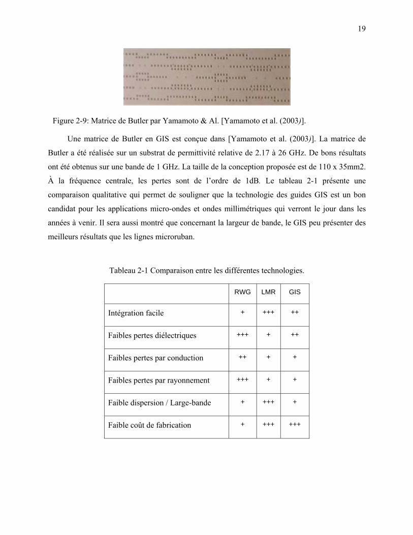
Figure 2-9: Matrice de Butler par Yamamoto & Al. [Yamamoto et al. (2003)].
Une matrice de Butler en GIS est conçue dans [Yamamoto et al. (2003)]. La matrice de
Butler a été réalisée sur un substrat de permittivité relative de 2.17 à 26 GHz. De bons résultats
ont été obtenus sur une bande de 1 GHz. La taille de la conception proposée est de 110 x 35mm2.
À la fréquence centrale, les pertes sont de l’ordre de 1dB. Le tableau 2-1 présente une
comparaison qualitative qui permet de souligner que la technologie des guides GIS est un bon
candidat pour les applications micro-ondes et ondes millimétriques qui verront le jour dans les
années à venir. Il sera aussi montré que concernant la largeur de bande, le GIS peu présenter des
meilleurs résultats que les lignes microruban.
Tableau 2-1 Comparaison entre les différentes technologies.
RWG LMR GIS
Intégration facile + +++ ++
Faibles pertes diélectriques +++ + ++
Faibles pertes par conduction ++ + +
Faibles pertes par rayonnement +++ + +
Faible dispersion / Large-bande + +++ +
Faible coût de fabrication + +++ +++
20
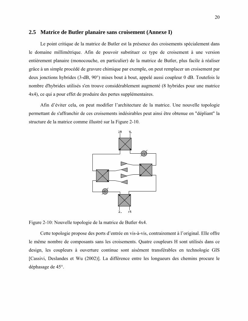
2.5 Matrice de Butler planaire sans croisement (Annexe I)
Le point critique de la matrice de Butler est la présence des croisements spécialement dans
le domaine millimétrique. Afin de pouvoir substituer ce type de croisement à une version
entièrement planaire (monocouche, en particulier) de la matrice de Butler, plus facile à réaliser
grâce à un simple procédé de gravure chimique par exemple, on peut remplacer un croisement par
deux jonctions hybrides (3-dB, 90°) mises bout à bout, appelé aussi coupleur 0 dB. Toutefois le
nombre d'hybrides utilisés s'en trouve considérablement augmenté (8 hybrides pour une matrice
4x4), ce qui a pour effet de produire des pertes supplémentaires.
Afin d’éviter cela, on peut modifier l’architecture de la matrice. Une nouvelle topologie
permettant de s'affranchir de ces croisements indésirables peut ainsi être obtenue en "dépliant" la
structure de la matrice comme illustré sur la Figure 2-10.
Figure 2-10: Nouvelle topologie de la matrice de Butler 4x4.
Cette topologie propose des ports d’entrée en vis-à-vis, contrairement à l’original. Elle offre
le même nombre de composants sans les croisements. Quatre coupleurs H sont utilisés dans ce
design, les coupleurs à ouverture continue sont aisément transférables en technologie GIS
[Cassivi, Deslandes et Wu (2002)]. La différence entre les longueurs des chemins procure le
déphasage de 45°.
21
Cette matrice est utilisée pour alimenter un réseau d’antenne à fentes. En alternant la
disposions des fentes, cela permet d’élargir la bande. Cette topologie présente le problème majeur
de ne pas être extensible à des matrices plus grandes (une matrice 8x8 par exemple).
2.6 Matrice de Butler en deux couches (Annexe II)
Pour réduire les dimensions, nous proposons une autre solution sans croisements. Dans ce
design nous combinons un coupleur plan-H avec un coupleur plan-E. Le coupleur consiste en
deux fentes dans la paroi du guide d’ondes. Le fait que les fentes sont disposées en symétrie au
lieu d’être disposée en longueur offre un coupleur très compact. Les vias le long du coupleur sont
utilisés comme trous d’alignement et comme un joint mécanique qui rassemble les guides
d’ondes ensemble. Cela évite l’utilisation d’une colle qui génère un gap et affecte énormément
les résultats.
Nous rassemblons les deux coupleurs. Comme premier test, nous avons utilisé des antennes
ALTSA (Antipodal linear tapered slot antenna). Ces antennes sont des antennes très large bande
qui nous permettront de mesurer les performances de la matrice. Comme deuxième test, un
réseau d’antennes fentes est utilisé. L’effet de la disposition du réseau sur deux plans sur l’angle
Figure 2-11: la topologie de la matrice de Butler avec des coupleurs 0 dB.
22
de pointage est étudié. Les résultats de mesure sont très prometteurs pour la conception d’une
matrice d’un plus grand ordre N.
2.7 Matrice de Butler planaire avec croisements (Annexe III)
L’utilisation des coupleurs 0 dB permet la réalisation d’une matrice totalement planaire. La
Figure:2-11 montre le schéma de cette matrice avec son réseau d’antennes. On constate la
disparition des croisements au profit des coupleurs (3-dB, 90°). Cependant, cette architecture a
doublé le nombre de coupleurs (huit à l’arrivée). De ce fait, on peut s’attendre à des pertes plus
importantes au niveau de la matrice et à une variation des pondérations en amplitude sur les
éléments rayonnants plus élevés.
Le guide GIS, tel que défini, présente toujours un certain niveau de pertes par ondes de
fuite à travers les rangées de trous. Ce niveau est en fonction de l’espacement entre les trous et
de leur diamètre. Dans l’éventualité où des guides GIS sont utilisés côte à côte comme dans la
matrice 2x2 présentée dans la Figure 2-3, ou dans le design présenté dans la Figure 2-9, ces ondes
de fuite peuvent causer un phénomène de diaphonie. Le niveau de diaphonie entre les guides GIS
est proportionnel à leurs longueurs. Ce constat n’a rien de surprenant et est bien exploité dans la
conception des coupleurs micro-ondes (les coupleurs à ouverture). On remarque également que le
niveau de couplage est assez faible. Dans les exemples présentés, la matrice de 2x2 et la matrice
4x4 dans la Figure 2-9, les structures sont des longs guides adjacents, ce qui nous porte à croire
que nous aurons des problèmes associés à cet aspect. En plus, en cas d’imperfection quelconque
les pertes augmentent considérablement.
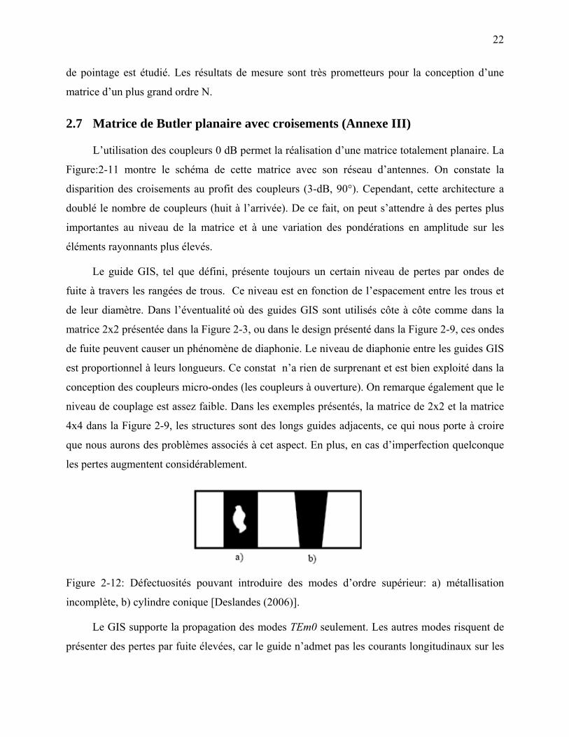
Figure 2-12: Défectuosités pouvant introduire des modes d’ordre supérieur: a) métallisation
incomplète, b) cylindre conique [Deslandes (2006)].
Le GIS supporte la propagation des modes TEm0 seulement. Les autres modes risquent de
présenter des pertes par fuite élevées, car le guide n’admet pas les courants longitudinaux sur les
23
murs latéraux. En théorie, ces modes d’ordre supérieur ne sont pas excités dans les structures qui
ne possèdent que des discontinuités dans le plan-H. Cependant, les procédés de fabrication ne
sont pas parfaits et des défectuosités, telles que celles illustrées à la Figure 2-12 peuvent
apparaître sur les circuits construits. Ces discontinuités risquent d’exciter les modes TEmn et
TMmn et, conséquemment, d’augmenter les pertes par fuite [Deslandes (2006)].
Ces phénomènes peuvent être aggravés avec les effets du temps, des chocs ou la fatigue
thermique. Cela nous pousse à prendre en considération une topologie avec des lignes GIS qui ne
sont pas côte à côte correspond mieux aux contraintes. Si un trou n’est pas bien plaqué, la phase
est affectée de 5 degrés et ainsi que l’amplitude est affectée modérément. Avec deux trous en
série, l’amplitude présente des variations très importantes avec des bandes interdites.
Le coupleur utilisé dans cette matrice est un coupleur en croix développé au cours de notre
travail. Le coupleur présente l’avantage d’être très compact puisque le couplage se passe dans la
section du croisement de deux Guides Intégrés au Substrat (GIS). Deux vias dans la section du
croisement permettent de diriger le flux du signal et de faire un ajustement du déphasage. Deux
autres vias sont placés dans chaque port afin de diminuer les réflexions en changeant la largeur de
la section.
La matrice est la combinaison de quatre coupleurs H en croix, ainsi que deux coupleurs
0dB. Ces composants sont reliés de façon à obtenir les plus petites dimensions possibles.

24
CHAPITRE 3
3. MATRICE DE BLASS ET NOLEN
La matrice de Blass et la matrice de Nolen contrairement à la matrice de Butler sont des
matrices d’alimentation en série; nous présentons dans ce chapitre la matrice de Nolen qui est un
cas particulier de la matrice de Blass, une des matrices les moins étudiées. On présente aussi une
définition de la largeur de bande d’une matrice suivant la stabilité de l’angle de pointage. Cette
définition est utile pour les réseaux d’alimentation d’antennes en série.
3.1 Matrice de Blass
La matrice de Blass [Blass (1960)] et [Blass (1971)] est un réseau d'alimentation en série
avec une structure en treillis comme celle illustré à la Figure 3-1. La matrice comporte plusieurs
lignes principales (ou lignes transverses "through lines" en anglais) qui transportent l'énergie et
plusieurs lignes secondaires (ou lignes de ramification "branch line" en anglais) qui croisent les
premières et mènent au réseau d'éléments rayonnants. Des coupleurs sont placés à chaque
croisement pour qu'une fraction de l'énergie incidente sur une ligne principale soit dirigée sur une
ligne secondaire dans un sens bien déterminé, vers un élément rayonnant placé à une extrémité de
cette ligne secondaire. Ces coupleurs déterminent la distribution en amplitude du réseau
d’antennes et par conséquent le niveau des lobes secondaires des diagrammes de rayonnement.
L'autre extrémité de la ligne secondaire est pourvue d'une charge absorbante. Entre deux
coupleurs directionnels, se situe un déphaseur ou un ajusteur de longueur de ligne engendrant le
changement de phase nécessaire à la création du gradient de phase entre chaque port de sortie.
Les coefficients de couplage des différents coupleurs et les valeurs de déphasage des différents
déphaseurs constants ou variables sont calculés de manière à obtenir les diagrammes de
rayonnement désirés qui sont différents selon que l'énergie arrive ou est prélevée par l'une ou
l'autre des lignes principales.
On notera que pour le port M d’entrée de la matrice, le diagramme de rayonnement désiré
est atteint sans difficulté. Le port M-1 sera lui affecté par le réseau d’alimentation du port n°M.
Cette affectation a été calculée par Blass [Blass (1971)] pour une distribution de coupleurs
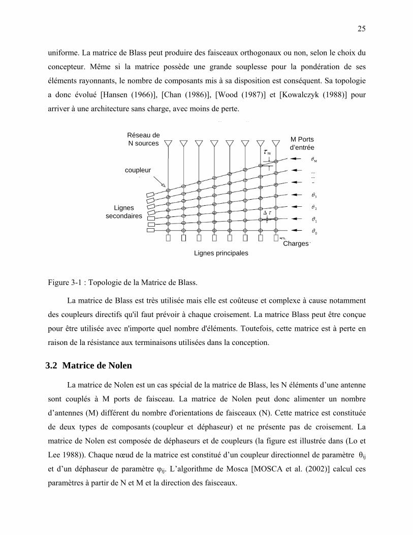
25
uniforme. La matrice de Blass peut produire des faisceaux orthogonaux ou non, selon le choix du
concepteur. Même si la matrice possède une grande souplesse pour la pondération de ses
éléments rayonnants, le nombre de composants mis à sa disposition est conséquent. Sa topologie
a donc évolué [Hansen (1966)], [Chan (1986)], [Wood (1987)] et [Kowalczyk (1988)] pour
arriver à une architecture sans charge, avec moins de perte.
Charges
Réseau deN sources M Ports
d’entrée
coupleur
Lignes principales
Lignessecondaires
Figure 3-1 : Topologie de la Matrice de Blass.
La matrice de Blass est très utilisée mais elle est coûteuse et complexe à cause notamment
des coupleurs directifs qu'il faut prévoir à chaque croisement. La matrice Blass peut être conçue
pour être utilisée avec n'importe quel nombre d'éléments. Toutefois, cette matrice est à perte en
raison de la résistance aux terminaisons utilisées dans la conception.
3.2 Matrice de Nolen
La matrice de Nolen est un cas spécial de la matrice de Blass, les N éléments d’une antenne
sont couplés à M ports de faisceau. La matrice de Nolen peut donc alimenter un nombre
d’antennes (M) différent du nombre d'orientations de faisceaux (N). Cette matrice est constituée
de deux types de composants (coupleur et déphaseur) et ne présente pas de croisement. La
matrice de Nolen est composée de déphaseurs et de coupleurs (la figure est illustrée dans (Lo et
Lee 1988)). Chaque nœud de la matrice est constitué d’un coupleur directionnel de paramètre θij
et d’un déphaseur de paramètre φij. L’algorithme de Mosca [MOSCA et al. (2002)] calcul ces
paramètres à partir de N et M et la direction des faisceaux.
26
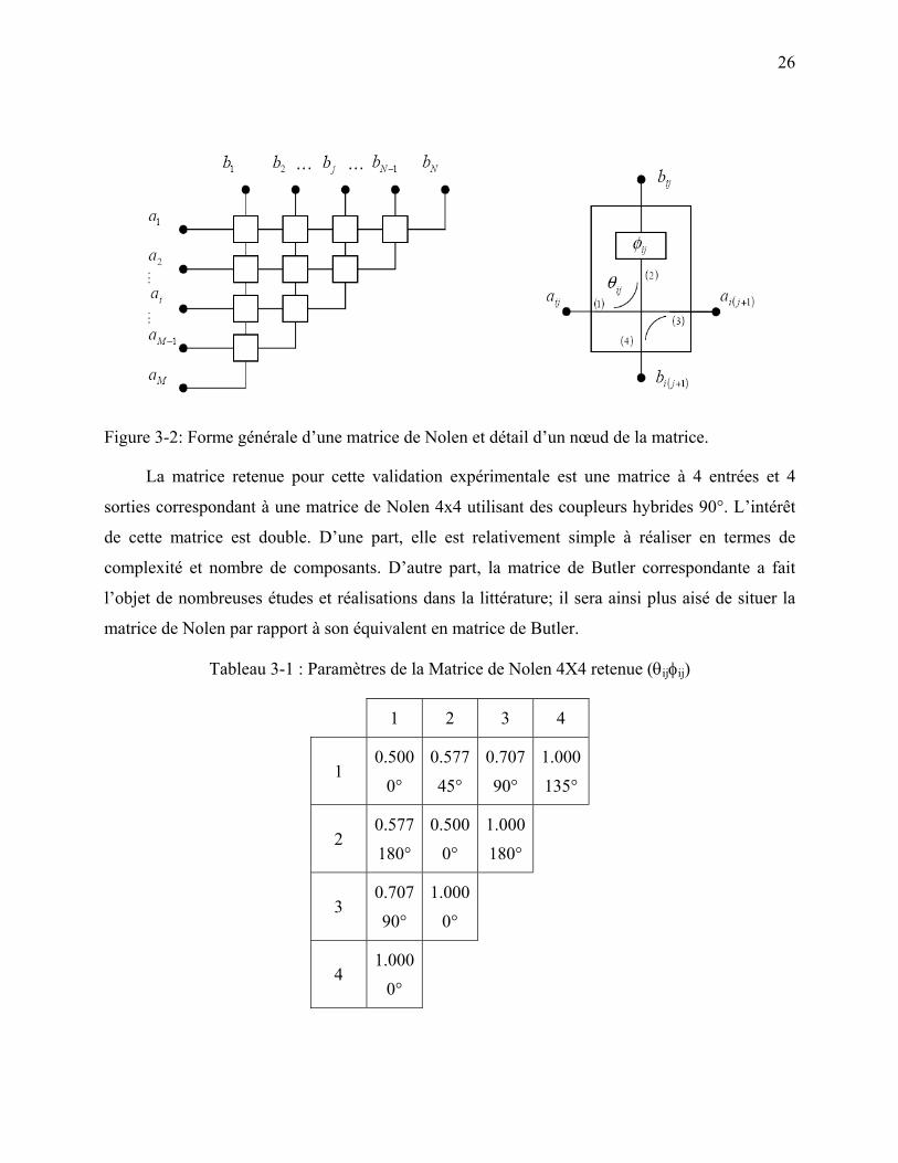
Figure 3-2: Forme générale d’une matrice de Nolen et détail d’un nœud de la matrice.
La matrice retenue pour cette validation expérimentale est une matrice à 4 entrées et 4
sorties correspondant à une matrice de Nolen 4x4 utilisant des coupleurs hybrides 90°. L’intérêt
de cette matrice est double. D’une part, elle est relativement simple à réaliser en termes de
complexité et nombre de composants. D’autre part, la matrice de Butler correspondante a fait
l’objet de nombreuses études et réalisations dans la littérature; il sera ainsi plus aisé de situer la
matrice de Nolen par rapport à son équivalent en matrice de Butler.
Tableau 3-1 : Paramètres de la Matrice de Nolen 4X4 retenue (θijφij)
1 2 3 4
1 0.500
0°
0.577
45°
0.707
90°
1.000
135°
2 0.577
180°
0.500
0°
1.000
180°
3 0.707
90°
1.000
0°
4 1.000
0°

27
Les paramètres théoriques des coupleurs directionnels et déphaseurs obtenus pour la
matrice décrite ci-dessus sont reportés dans le Tableau 1. Ces valeurs indiquent que 3 coupleurs
directionnels différents sont nécessaires pour réaliser cette matrice, ainsi que 4 déphaseurs
différents, soit un total de 7 composants différents à optimiser.
3.3 Largeur de bande
La bande passante d’un réseau d’antenne dépend du type d’éléments utilisés, tel que les
déphaseurs et le réseau d’alimentation d’antenne. La plupart de ces éléments sont conçus sur une
large bande de fréquence comme dans notre cas. La largeur de bande des éléments n’est pas le
principal facteur dans la détermination de la bande passante. Les limitations de la bande passante
sont déterminées par les caractéristiques en fréquence des déphaseurs et des réseaux
d’alimentation.
Si on considère un réseau de N éléments séparé de d, la différence de phase entre chaque deux
éléments adjacents pour réaliser un rayonnement dans la direction θ est :
( 2 / ) sin( )d c fϕ π θΔ = − (1)
où f est la fréquence et c la vitesse de la lumière dans le vide.
Si la fréquence change par fΔ et l’angle du pointage de θΔ avec une déviation de la phase de
δϕ :
( ) ( 2 / )( ) sin( )d c f fϕ δϕ π θ θΔ + = − + Δ + Δ (2)
Si la phase est indépendante de la fréquence 0δϕ = , les équations (1) et (2) sont égales, ce qui
donne :
sin( ) ( ) sin( )f f fθ θ θ= + Δ + Δ (3)
Cela signifie que la variation du pointage est exprimée par:
[ ]1sin sin( ) / (1 / )f fθ θ θ−Δ = − + +Δ (4)
L’augmentation de l’angle du pointage où de la largeur de bande en utilisant des déphaseurs
constants augmente significativement l’erreur du pointage. Donc l’utilisation de déphaseur
constant avec la fréquence n’offre pas la solution désirée.

28
Si on suppose qu’il y a une variation de phase qui n’engendre pas une variation dans la direction
du pointage (2) devient :
( ) ( 2 / )( ) sin( )d c f fϕ δϕ π θΔ + = − + Δ (5)
de (1) et (5) on a :
( 2 / ) sin( )d c fδϕ π θ= − Δ (6)
d est au maximum égal à λ (pour contrôler le niveau des lobes secondaires), l’équation (6)
devient :
2 sin( )f
fδϕ π θΔ
=− (7)
Pour un pointage à 0°, gradient de phase doit être nul. À l’angle θ la bande réel est définit en
terme d’erreur du pointage:
sin( )2
ff
δϕθ π
Δ= (8)
Dans les matrices de Nolen proposées, les différentes voies n’ont pas les mêmes longueurs. On
peut définir l’erreur de pointage et de là imposer les longueurs de ligne.
3.4 Matrice de Nolen en treillis (Annexe IV)
Cette matrice de Nolen est basée sur une topologie conventionnelle en treillis. Elle sera
conçue à la fréquence centrale de 12.5 GHz avec 0.5GHz de largeur de bande. Les coupleurs
utilisés ont déjà un déphasage de 90°, donc il faudra prendre en considération ce point. Le
coupleur utilisé est un coupleur en croix. Des couplages de 3dB, 4.77 dB et 6.02 dB ont été
optimisés.
Le coupleur utilisé est un coupleur en croix. Des couplages de 3dB, 4.77 dB et 6.02 dB
ont été optimisés. Pour le coupleur coudé, on a gardé le même concept; on ajoute quatre coudes
aux ports du coupleur pour l’adapter à la géométrie de notre matrice.

29
3.5 Matrice de Nolen large bande (Annexe V)
La solution proposée est une matrice où les différents chemins doivent être égaux le plus
possible. Une architecture quasi parallèle est utilisée dans cette matrice. Une compensation du
délai engendré par les coupleurs assurera un comportement large bande. L’avantage de cette
matrice est qu’elle présente des performances comparables à celle de la matrice de Butler avec la
possibilité de concevoir des matrices avec n’importe quelle combinaison NxM.
La matrice est conçue à la fréquence centrale de 76GHz. Des coupleurs plan-H de type
Riblet sont utilisés. Aussi les différents déphaseurs doivent être distribués de la même façon, des
déphaseurs additionnels sont nécessaires.
30
CHAPITRE 4
4. MATRICE DE BUTLER AVEC UN NIVEAU DE LOBES LATERAUX
CONTROLÉ
Le niveau général des lobes secondaires décrit la sensibilité de l'antenne au brouillage (en
télécommunications) ou la finesse d'imagerie (en radar). La matrice de Butler est utilisée pour
améliorer le niveau du signal/bruit. Mais comme le montrent les résultats des matrices
développées au cours du présent travaille ou dans les références, la matrice montre des niveaux
de lobes latéraux (Side Lobe Level (SLL)) élevés. En effet un réseau uniforme présente un SLL
de -13.6 dB mais dû à l’utilisation d’un déphaseur progressif et le couplage mutuel entre les
antennes le SLL est entre -5 et -10dB, comme le montre les résultats des matrices présentées dans
les chapitres 3 et 4.
4.1 Matrice de Butler avec un bas SLL basé sur l’augmentation du nombre de
ports de sortie
Il y a plusieurs types de modifications qu’on peut apporter à une matrice de Butler pour
réduire le niveau de lobes secondaire à un niveau acceptable.
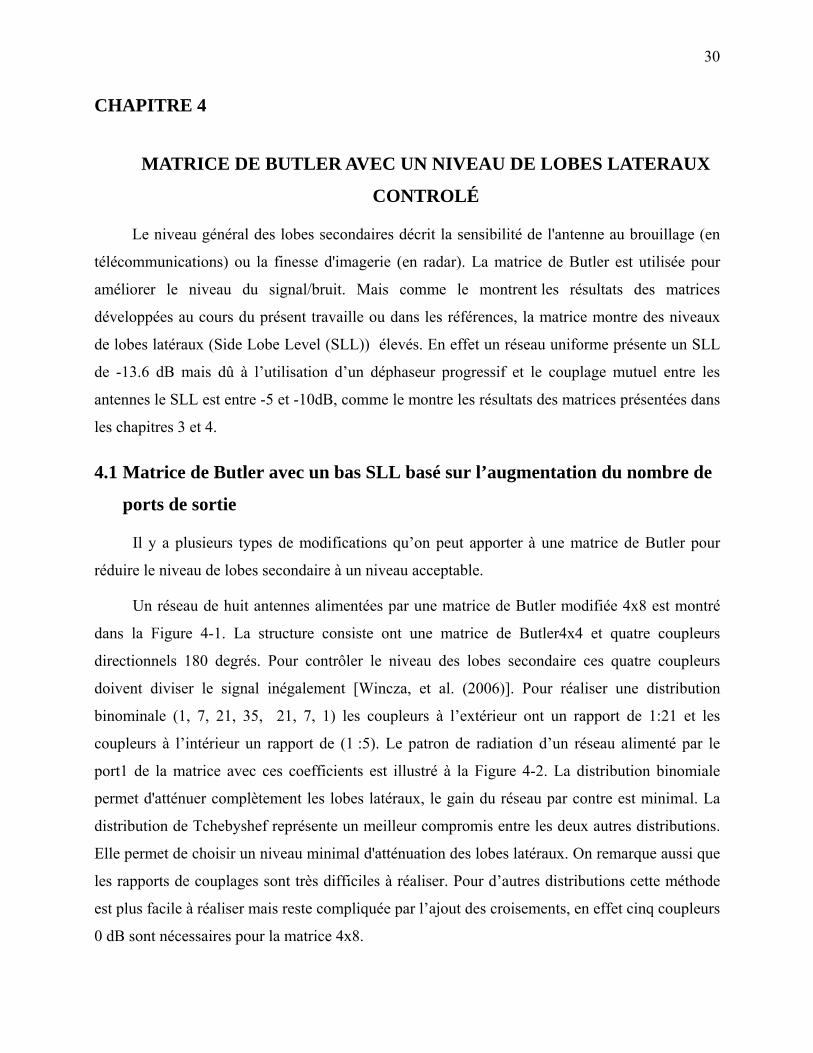
Un réseau de huit antennes alimentées par une matrice de Butler modifiée 4x8 est montré
dans la Figure 4-1. La structure consiste ont une matrice de Butler4x4 et quatre coupleurs
directionnels 180 degrés. Pour contrôler le niveau des lobes secondaire ces quatre coupleurs
doivent diviser le signal inégalement [Wincza, et al. (2006)]. Pour réaliser une distribution
binominale (1, 7, 21, 35, 21, 7, 1) les coupleurs à l’extérieur ont un rapport de 1:21 et les
coupleurs à l’intérieur un rapport de (1 :5). Le patron de radiation d’un réseau alimenté par le
port1 de la matrice avec ces coefficients est illustré à la Figure 4-2. La distribution binomiale
permet d'atténuer complètement les lobes latéraux, le gain du réseau par contre est minimal. La
distribution de Tchebyshef représente un meilleur compromis entre les deux autres distributions.
Elle permet de choisir un niveau minimal d'atténuation des lobes latéraux. On remarque aussi que
les rapports de couplages sont très difficiles à réaliser. Pour d’autres distributions cette méthode
est plus facile à réaliser mais reste compliquée par l’ajout des croisements, en effet cinq coupleurs
0 dB sont nécessaires pour la matrice 4x8.
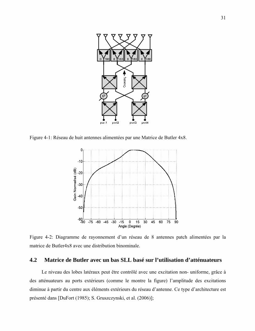
31
ϕϕ
Figure 4-1: Réseau de huit antennes alimentées par une Matrice de Butler 4x8.
Figure 4-2: Diagramme de rayonnement d’un réseau de 8 antennes patch alimentées par la
matrice de Butler4x8 avec une distribution binominale.
4.2 Matrice de Butler avec un bas SLL basé sur l’utilisation d’atténuateurs
Le niveau des lobes latéraux peut être contrôlé avec une excitation non- uniforme, grâce à
des atténuateurs au ports extérieurs (comme le montre la figure) l’amplitude des excitations
diminue à partir du centre aux éléments extérieurs du réseau d’antenne. Ce type d’architecture est
présenté dans [DuFort (1985); S. Gruszczynski, et al. (2006)];
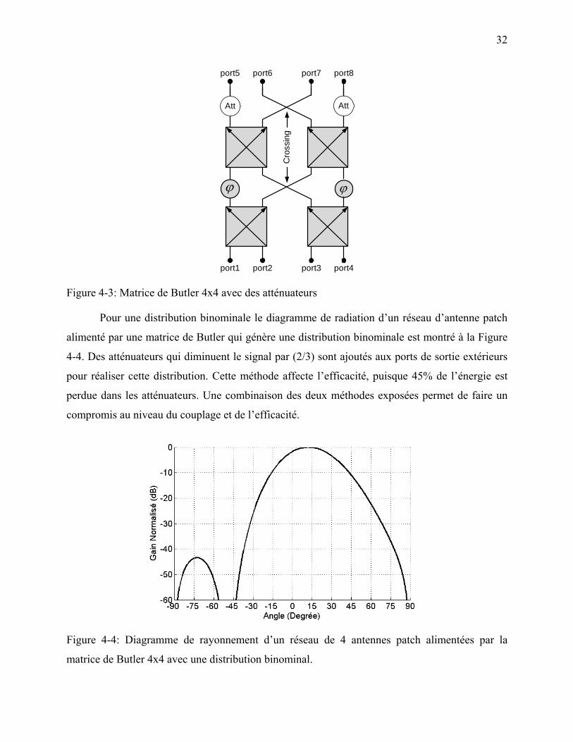
32
ϕϕ
port1 port2 port3 port4
port5 port6 port7 port8
Cro
ssin
g
Att Att
Figure 4-3: Matrice de Butler 4x4 avec des atténuateurs
Pour une distribution binominale le diagramme de radiation d’un réseau d’antenne patch
alimenté par une matrice de Butler qui génère une distribution binominale est montré à la Figure
4-4. Des atténuateurs qui diminuent le signal par (2/3) sont ajoutés aux ports de sortie extérieurs
pour réaliser cette distribution. Cette méthode affecte l’efficacité, puisque 45% de l’énergie est
perdue dans les atténuateurs. Une combinaison des deux méthodes exposées permet de faire un
compromis au niveau du couplage et de l’efficacité.
Figure 4-4: Diagramme de rayonnement d’un réseau de 4 antennes patch alimentées par la
matrice de Butler 4x4 avec une distribution binominal.
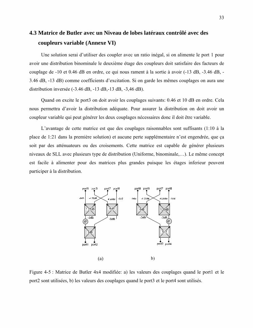
33
4.3 Matrice de Butler avec un Niveau de lobes latéraux contrôlé avec des
coupleurs variable (Annexe VI)
Une solution serai d’utiliser des coupler avec un ratio inégal, si on alimente le port 1 pour
avoir une distribution binominale le deuxième étage des coupleurs doit satisfaire des facteurs de
couplage de -10 et 0.46 dB en ordre, ce qui nous rament à la sortie à avoir (-13 dB, -3.46 dB, -
3.46 dB, -13 dB) comme coefficients d’excitation. Si on garde les mêmes couplages on aura une
distribution inversée (-3.46 dB, -13 dB,-13 dB, -3,46 dB).
Quand on excite le port3 on doit avoir les couplages suivants: 0.46 et 10 dB en ordre. Cela
nous permettra d’avoir la distribution adéquate. Pour assurer la distribution on doit avoir un
coupleur variable qui peut générer les deux couplages nécessaires donc il doit être variable.
L’avantage de cette matrice est que des couplages raisonnables sont suffisants (1:10 à la
place de 1:21 dans la première solution) et aucune perte supplémentaire n’est engendrée, que ça
soit par des atténuateurs ou des croisements. Cette matrice est capable de générer plusieurs
niveaux de SLL avec plusieurs type de distribution (Uniforme, binominale,…). Le même concept
est facile à alimenter pour des matrices plus grandes puisque les étages inferieur peuvent
participer à la distribution.
ϕ ϕ
(a) b)
Figure 4-5 : Matrice de Butler 4x4 modifiée: a) les valeurs des couplages quand le port1 et le
port2 sont utilisées, b) les valeurs des couplages quand le port3 et le port4 sont utilisés.
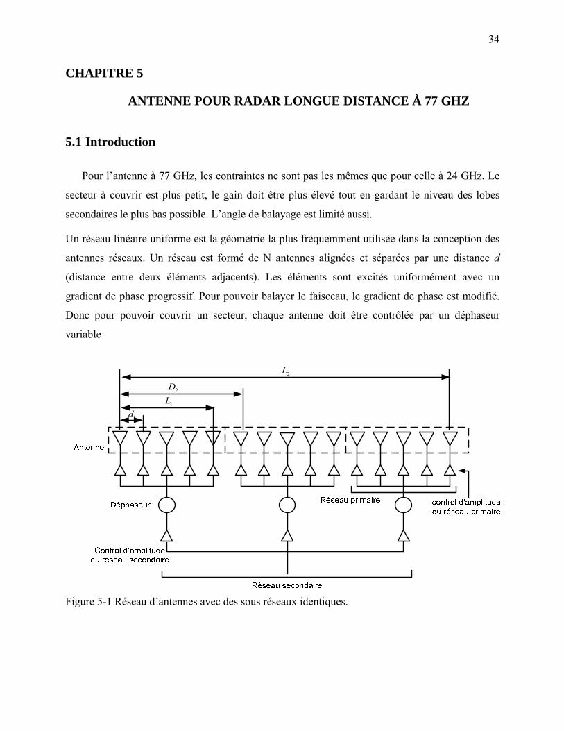
34
CHAPITRE 5
5. ANTENNE POUR RADAR LONGUE DISTANCE À 77 GHZ
5.1 Introduction
Pour l’antenne à 77 GHz, les contraintes ne sont pas les mêmes que pour celle à 24 GHz. Le
secteur à couvrir est plus petit, le gain doit être plus élevé tout en gardant le niveau des lobes
secondaires le plus bas possible. L’angle de balayage est limité aussi.
Un réseau linéaire uniforme est la géométrie la plus fréquemment utilisée dans la conception des
antennes réseaux. Un réseau est formé de N antennes alignées et séparées par une distance d
(distance entre deux éléments adjacents). Les éléments sont excités uniformément avec un
gradient de phase progressif. Pour pouvoir balayer le faisceau, le gradient de phase est modifié.
Donc pour pouvoir couvrir un secteur, chaque antenne doit être contrôlée par un déphaseur
variable
Figure 5-1 Réseau d’antennes avec des sous réseaux identiques.
1d
2D
1L
2L
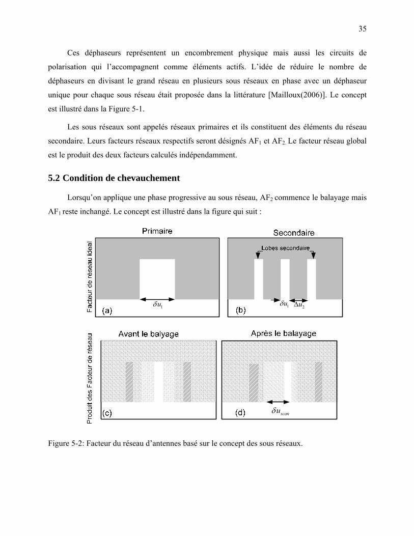
35
Ces déphaseurs représentent un encombrement physique mais aussi les circuits de
polarisation qui l’accompagnent comme éléments actifs. L’idée de réduire le nombre de
déphaseurs en divisant le grand réseau en plusieurs sous réseaux en phase avec un déphaseur
unique pour chaque sous réseau était proposée dans la littérature [Mailloux(2006)]. Le concept
est illustré dans la Figure 5-1.
Les sous réseaux sont appelés réseaux primaires et ils constituent des éléments du réseau
secondaire. Leurs facteurs réseaux respectifs seront désignés AF1 et AF2. Le facteur réseau global
est le produit des deux facteurs calculés indépendamment.
5.2 Condition de chevauchement
Lorsqu’on applique une phase progressive au sous réseau, AF2 commence le balayage mais
AF1 reste inchangé. Le concept est illustré dans la figure qui suit :
1uδ 1uδ2uΔ
scanuδ
Figure 5-2: Facteur du réseau d’antennes basé sur le concept des sous réseaux.

36
i i iL N d= ×
id Représente l’espacement entre les éléments. Ni correspond au nombre d’éléments dans le
réseau primaire (i=1) et le réseau secondaire.
Le facteur de réseau peut être remplacé par une fonction porte idéale définie comme suit :
( )1, ( 1) cos 1 ; 0, 1, 2,...
( )0,
ii i
i
LqN qN qAF
autre
π π γ πγ λ
⎧ − ≤ ≤ + = ± ±⎪= ⎨⎪⎩
avec 0 γ π≤ ≤
La périodicité de cette fonction est responsable des lobes secondaires.
On définit l’angle de réseau u :
2 cosu π γλ
=
La périodicité du facteur réseau AF2 en fonction de de u est donnée par :
2 2 22 /u N LπΔ =
avec une largeur du facteur du réseau primaire AF1 qui correspond à 11 4 /u Lδ π=
La largeur de balayage scanuδ est la distance entre les centres du rayonnement aux extrémités du
balayage.
Nous assumons pour que les lobes secondaires du facteur AF2 reçoivent suffisamment
d'atténuation, tant qu’au moins la moitié de sa largeur du faisceau ne tombe pas dans le faisceau
principal du facteur AF1. Cette condition s’écrit :
( )2 112 scanu u uδ δΔ ≥ +
en d’autres termes, on peut écrire que
( ) 12 1
2uu δαΔ ≥ +
(1)
(2)
(3)
(5)
(4)
(6)

37
et en termes de paramètres du réseau
( ) 21 2
2
1 (1 )LL dN
α α≥ + = +
Cette équation représente la condition sur la longueur du réseau et l’espacement pour éviter les
lobes secondaires dans le facteur global.
Le facteur de chevauchement CC est défini comme :
1
2
1LCCd
= −
Ce dernier représente la fraction de la longueur d'un sous réseau qui se superpose avec chacun
des sous réseaux adjacents. Pour un réseau non chevauchant CC≤0.
Le facteur de chevauchement s’écrira comme suit :
1
scanuCCu
δαδ
≥ =
Cela montre que pour chaque balayage, le réseau doit présenter un chevauchement pour pouvoir
diminuer le niveau des lobes secondaires.
Donc pour concevoir notre antenne, nous avons besoin d’une alimentation avec une
distribution et un coupleur 0 dB qui assure le chevauchement.
5.3 Modes d’alimentation
Dans notre cas, les contraintes d’alimentation supposent que :
- Les différents éléments des sous réseaux sont en phase
- Une distribution d’amplitude est à engendrer pour satisfaire le critère de lobes latéraux
5.3.1 Réseaux d’alimentation avec recombinaison (Annexe VII)
Une distribution binominale est générée dans notre guide d’alimentation. Le réseau
d’alimentation est basé sur l’assemblage de plusieurs diviseurs en Y. Avec la même topologie, on
a pu générer différentes distributions (triangulaire, Tchebychev, Taylor).
(7)
(8)
(9)
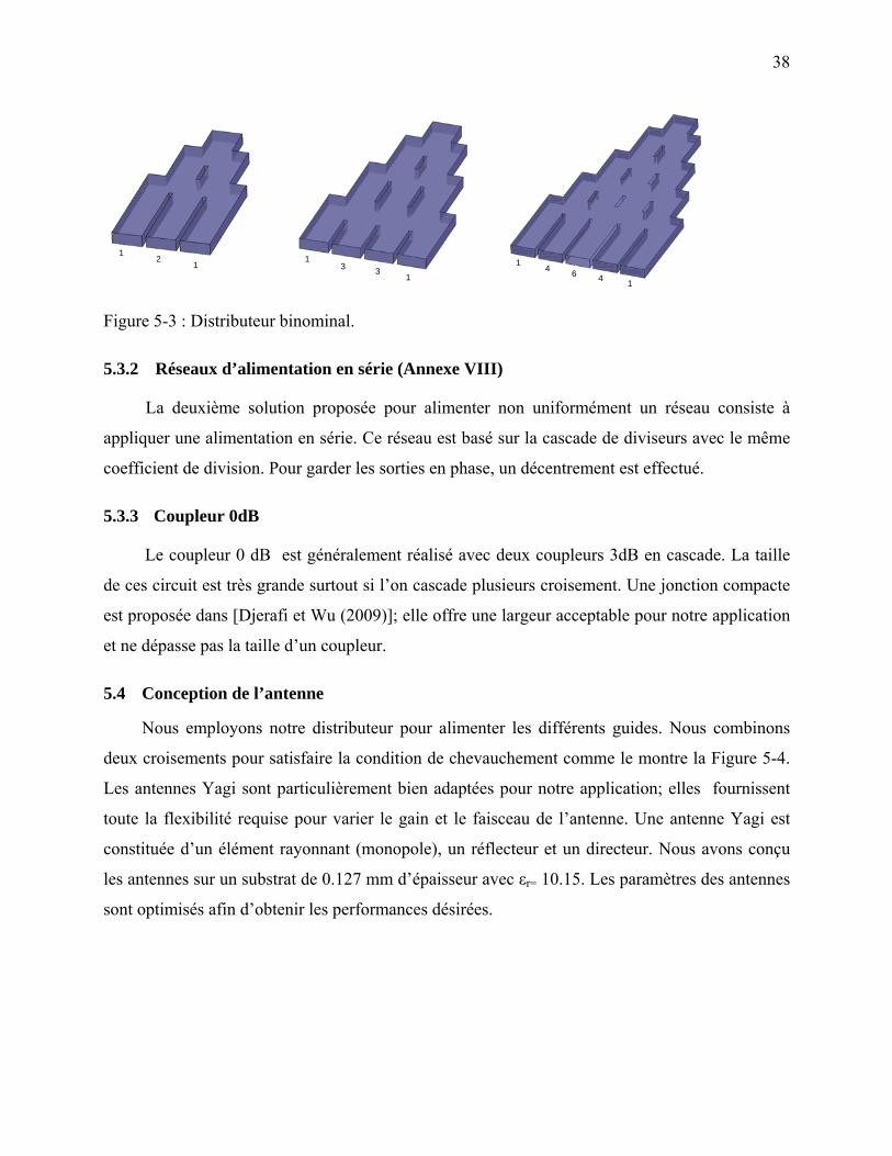
38
14 6
11
1
233 1
14
Figure 5-3 : Distributeur binominal.
5.3.2 Réseaux d’alimentation en série (Annexe VIII)
La deuxième solution proposée pour alimenter non uniformément un réseau consiste à
appliquer une alimentation en série. Ce réseau est basé sur la cascade de diviseurs avec le même
coefficient de division. Pour garder les sorties en phase, un décentrement est effectué.
5.3.3 Coupleur 0dB
Le coupleur 0 dB est généralement réalisé avec deux coupleurs 3dB en cascade. La taille
de ces circuit est très grande surtout si l’on cascade plusieurs croisement. Une jonction compacte
est proposée dans [Djerafi et Wu (2009)]; elle offre une largeur acceptable pour notre application
et ne dépasse pas la taille d’un coupleur.
5.4 Conception de l’antenne
Nous employons notre distributeur pour alimenter les différents guides. Nous combinons
deux croisements pour satisfaire la condition de chevauchement comme le montre la Figure 5-4.
Les antennes Yagi sont particulièrement bien adaptées pour notre application; elles fournissent
toute la flexibilité requise pour varier le gain et le faisceau de l’antenne. Une antenne Yagi est
constituée d’un élément rayonnant (monopole), un réflecteur et un directeur. Nous avons conçu
les antennes sur un substrat de 0.127 mm d’épaisseur avec εr= 10.15. Les paramètres des antennes
sont optimisés afin d’obtenir les performances désirées.
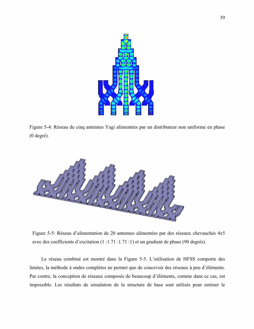
39
Figure 5-4: Réseau de cinq antennes Yagi alimentées par un distributeur non uniforme en phase
(0 degré).
Figure 5-5: Réseau d’alimentation de 20 antennes alimentées par des réseaux chevauchés 4x5
avec des coefficients d’excitation (1 :1.71 :1.71 :1) et un gradient de phase (90 degrés).
Le réseau combiné est montré dans la Figure 5-5. L’utilisation de HFSS comporte des
limites, la méthode à ondes complètes ne permet que de concevoir des réseaux à peu d’éléments.
Par contre, la conception de réseaux composés de beaucoup d’éléments, comme dans ce cas, est
impossible. Les résultats de simulation de la structure de base sont utilisés pour estimer le
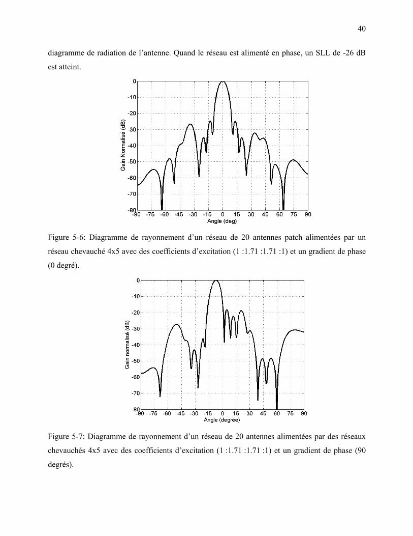
40
diagramme de radiation de l’antenne. Quand le réseau est alimenté en phase, un SLL de -26 dB
est atteint.
Figure 5-6: Diagramme de rayonnement d’un réseau de 20 antennes patch alimentées par un
réseau chevauché 4x5 avec des coefficients d’excitation (1 :1.71 :1.71 :1) et un gradient de phase
(0 degré).
Figure 5-7: Diagramme de rayonnement d’un réseau de 20 antennes alimentées par des réseaux
chevauchés 4x5 avec des coefficients d’excitation (1 :1.71 :1.71 :1) et un gradient de phase (90
degrés).

41
Avec un gradient de phase de 90 degrés, on arrive à un angle de pointage de 8 degré qui
satisfait notre cahier de charge. Le niveau du SLL est de -18.9 dB ce qui est très acceptable. Le
défi au niveau de la conception de l’antenne globale est de réduire le couplage entre les réseaux
d’antennes.
Nous avons démontré la possibilité de concevoir un réseau d’antenne capable de satisfaire
les exigences de gain et de niveau de SLL avec une réduction considérable du nombre des
déphaseurs de 24 à juste 4.
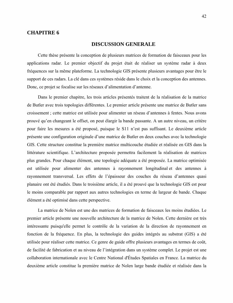
42
CHAPITRE 6
6. DISCUSSION GENERALE
Cette thèse présente la conception de plusieurs matrices de formation de faisceaux pour les
applications radar. Le premier objectif du projet était de réaliser un système radar à deux
fréquences sur la même plateforme. La technologie GIS présente plusieurs avantages pour être le
support de ces radars. La clé dans ces systèmes réside dans le choix et la conception des antennes.
Donc, ce projet se focalise sur les réseaux d’alimentation d’antenne.
Dans le premier chapitre, les trois articles présentés traitent de la réalisation de la matrice
de Butler avec trois topologies différentes. Le premier article présente une matrice de Butler sans
croissement ; cette matrice est utilisée pour alimenter un réseau d’antennes à fentes. Nous avons
prouvé qu’en changeant le offset, on peut élargir la bande passante. A un autre niveau, un critère
pour faire les mesures a été proposé, puisque le S11 n’est pas suffisant. Le deuxième article
présente une configuration originale d’une matrice de Butler en deux couches avec la technologie
GIS. Cette structure constitue la première matrice multicouche étudiée et réalisée en GIS dans la
littérature scientifique. L’architecture proposée permettra facilement la réalisation de matrices
plus grandes. Pour chaque élément, une topologie adéquate a été proposée. La matrice optimisée
est utilisée pour alimenter des antennes à rayonnement longitudinal et des antennes à
rayonnement transversal. Les effets de l’épaisseur des couches du réseau d’antennes quasi
planaire ont été étudiés. Dans le troisième article, il a été prouvé que la technologie GIS est pour
le moins comparable par rapport aux autres technologies en terme de largeur de bande. Chaque
élément a été optimisé dans cette perspective.
La matrice de Nolen est une des matrices de formation de faisceaux les moins étudiées. Le
premier article présente une nouvelle architecture de la matrice de Nolen. Cette dernière est très
intéressante puisqu'elle permet le contrôle de la variation de la direction de rayonnement en
fonction de la fréquence. En plus, la technologie des guides intégrés au substrat (GIS) a été
utilisée pour réaliser cette matrice. Ce genre de guide offre plusieurs avantages en termes de coût,
de facilité de fabrication et au niveau de l’intégration dans un système complet. Le projet est une
collaboration internationale avec le Centre National d'Études Spatiales en France. La matrice du
deuxième article constitue la première matrice de Nolen large bande étudiée et réalisée dans la

43
littérature scientifique. La solution proposée est une matrice où les différents chemins doivent
être le plus égaux possible. Une architecture quasi parallèle est utilisée dans cette matrice. Une
compensation du délai engendré par les coupleurs assurera un comportement très large bande.
L’avantage de cette matrice est qu’elle présente des performances comparables à celles de la
matrice de Butler, ajoutant la possibilité de concevoir des matrices avec n’importe quelle
combinaison NxM. La matrice est conçue à la fréquence centrale de 76 GHz.
Dans le quatrième chapitre, une nouvelle topologie des matrices à faible SLL est proposée
dans un article. Elle est basée sur un coupleur que nous avons présenté lors d’une conférence. Ce
coupleur est une nouvelle classe dans les coupleurs GIS, puisque il n’est pas basé sur les
ouvertures. Une version variable où les profondeurs des vis contrôlent le niveau du couplage est
présentée. L’objectif est de réaliser une matrice contrôlable électriquement. Ce travail est une
première étape dans cette direction.
Pour le radar longue distance, un gain élevé s’avère être nécessaire. Un réseau avec un plus
petit nombre de déphaseurs est proposé pour garder une bonne efficacité. Ce réseau est composé
de diviseurs non uniformes (deux articles) et de coupleurs 0 dB (le troisième article de ce
chapitre) afin de satisfaire la condition de chevauchement obligatoire pour garder un SLL
acceptable.
Nous avons réalisé la quasi-totalité des travaux de développement et de tests. Quant à la
rédaction de l’article, j’en ai écrit la première version; les co-auteurs y ont apporté leurs
corrections et m’ont formulé leurs suggestions.
44
CONCLUSIONS ET TRAVAUX FUTURS
Les antennes intelligentes à faisceau commutable présentent une solution de choix pour
systèmes radar. La réduction des interférences contribue à améliorer le rapport du signal sur bruit,
et par conséquent augmenter la capacité totale de ces systèmes sans l’utilisation de spectre
additionnel.
Dans le présent travail, nous avons exposé la conception de plusieurs matrices de Butler
en technologie « Guide d’ondes Intégré au Substrat ». Une jonction huit-port est utilisée comme
matrice de Butler. Cette matrice planaire est utilisée pour alimenter un réseau à fentes très large
bande à 77 GHz. Une comparaison des pertes par radiation d’un coude 90 degrés en GIS et un
coude en microstrip sont effectués; les faibles pertes en GIS montrent l’avantage d’utiliser cette
technologie dans les réseaux d’alimentation d’antenne. Les circuits multicouches présentent des
avantages comme la réduction de la taille ou de l’élargissement de la bande. Une matrice deux
couches a été présentée, elle est composée de deux coupleurs en plan-H et deux coupleurs en
plan-E. Le changement de couche nous permet de ne pas avoir recourt aux croisements. La
matrice est étudiée pour supporter des antennes à rayonnement transversal et des antennes à
rayonnement longitudinal. Pour réaliser une matrice de Butler planaire fonctionnant autour de la
fréquence 12.5 GHz un coupleur en croix a été développé. Ce coupleur a été utilisé pour réaliser
un couplage 0 dB. Ces éléments de base de la matrice ont été réalisés et mesurés. Ces coupleurs
affichent les résultats attendus sur une large bande. La matrice a été assemblée avec quatre
coupleurs en croix et deux coupleurs 0 dB combinés avec des déphaseurs GIS large bande. La
matrice a été optimisée, réalisée puis mesurée. Les résultats mesurés montrent une excellente
performance en amplitudes et en phases sur une bande de 3 GHz. Les effets des pondérations de
phase sur le rayonnement d’un réseau d’antennes alimenté par cette matrice ont été étudiés,
montrant un pointage très stable avec la fréquence. Son poids et ses performances font de la
matrice un excellent candidat pour alimenter un réseau d’antennes planaire. Ces performances
nous poussent à croire qu’une matrice d’ordre supérieure (8x8 ou 16x16) affichera une bonne
largeur de bande. Une réduction des dimensions est très faisable en utilisant un substrat avec une
permittivité plus élevée.
45
Nous avons proposé une nouvelle méthode pour diminuer le niveau des lobes secondaire
généré par un réseau d’antenne alimenté par des matrices de Butler. Cette méthode est basée sur
une combinaison de coupleurs variables. Pour cela une jonction avec le facteur de couplage
contrôlable a été proposée en guide d’onde métallique. Le coupleur est basé sur une technique
quasi-optique où un réseau de vis cylindriques est utilisé pour changer le couplage. Les résultats
de mesure ont été utilisés pour estimer les coefficients de transmission qu’une matrice de Butler
peut réaliser ainsi que les diagrammes de radiation. Cette matrice est sans perte additionnelle et
peut générer plusieurs niveaux de SLL.
Dans le présent travail nous avons présenté la conception, la construction et les mesures
d’une matrice de Nolen dans la bande 12.25-12.75 GHz en technologie GIS. Pour ce design, on
s’est basé sur les topologies standards proposées dans la littérature scientifique. Cette matrice a
été adaptée pour satisfaire les contraintes imposées par la technologie, principalement la
dimension globale limitée par la cuve sous pression utilisée dans le placage des trous. Les
différents éléments ont été conçus séparément. Par la suite l’ensemble de la matrice de Nolen a
été simulé et optimisé afin d’atteindre les performances désirées. Ces résultats de Nolen ont été
présentés et comparés aux simulations et aux valeurs théoriques. La réalisation de la matrice de
Nolen illustre bien le plein potentiel de la technologie GIS. Par la suite, une matrice large bande a
été proposée. Une compensation de délai engendrée par les coupleurs plan-H en parallèle a
permis de réduire la dispersion de phase, les amplitudes s’améliore puisque la matrice de Nolen
est basé sur une superposition des signaux.
Une architecture pour radar longue distance a été proposée avec une réduction du nombre
des déphaseurs utilisés. Pour ces radars on a besoin d’un SLL bas avec un petit angle de
balayage. Un critère de chevauchement est proposé pour pouvoir réaliser cette réduction. Le
concept de réduction de nombre des déphaseurs afin de réduire les pertes, l’efficacité, la
complexité et le coût a été prouvé.
Un travail systématique a été réalisé par Hall pour chaque type de perte dans un réseau
d’alimentation d’antenne en microruban. De plus, l’influence de ces pertes sur le rayonnement de
l’antenne au niveau du gain et du SLL est étudiée. Hall a démontré que pour un réseau planaire le
gain se sature avec une efficacité très faible. Un travail semblable est nécessaire pour quantifier et
démontrer les limites de la technologie GIS.

46
Notre première suggestion concerne la conception d’antennes des matrices de Nolen.
Comme étapes suivantes, il reste à redéfinir la matrice avec le paramètre de pointage d’antenne
comme contrainte (comme on a définit la largeur de bande en terme de variation de pointage).
Une distribution non-uniforme des amplitudes sera appropriée pour diminuer le niveau des lobes
secondaires. Des antennes intégrés à la matrice permettrons des mesures des diagrammes de
rayonnement et montreront les améliorations apportées par les GIS. Dans l’algorithme de Mosca
qui définit le couplage de chaque nœud dans une matrice de Blass ou Nolen, il faut prendre en
considération les pertes engendrées par les longueurs utilisées puisque les pertes du port d’entré
aux ports de sorties ne sont pas les mêmes vu qu’il s’agit d’une alimentation en série. Des
couplages différents de ceux calculés par Mosca peuvent être utilisés pour compenser ces pertes.
Une matrice de Butler modifiée a été proposée avec un coupleur variable mécaniquement.
Le même coupleur peut être réalisé en variant le couplage avec des diodes dans la région
commune. La variation électrique rendra la matrice très facile à réaliser. Pour une matrice de plus
grand ordre (8x8 ou plus) on doit dimensionner tous les paramètres pour déterminer le couplage
de chaque jonction dans ces matrices en fonction de la distribution choisie.
La matrice de Nolen large bande présente des avantage en terme de flexibilité par rapport
au nombre des ports d’entrées et sorties. L’association de cette matrice avec des délais variables,
permettra de changer la variation de la phase avec la fréquence et par conséquent la variation de
la direction de rayonnement. Cette matrice présente des ressemblances avec la matrice de Butler;
avec l’utilisation des coupleurs variables on peut passer d’un type à un autre.
La matrice de Butler est utilisée dans les réseaux d’amplificateurs distribués; une étude sur
l’énergie maximale supportée par les GIS est nécessaire. L’isolation des sorties des matrices est
très critique dans cette application. L’association de la matrice de Butler avec des amplificateurs
et la réalisation des mesures nécessaires offriront une ouverture pour la technologie GIS.
Toutes les matrice de Blass sont en multicouche. Les facteurs de couplage sont très
difficiles à réaliser avec un coupleur en plan-H. Le coupleur quasi-optique proposé peut très bien
réaliser les facteurs nécessaires pour une matrice complètement planaire. Le nombre de couches
doit être augmenté; chaque couche participe à la réflexion d’une partie de l’énergie et à
l’adaptation. Une matrice de Blass reconfigurable est envisageable avec le coupleur variable.

47
Pour l’antenne à nombre de déphaseurs réduit pour les applications à 77 GHz, des
déphaseurs doivent être réalisés à cette fréquence afin de les intégrer à l’antenne. Cela permettra
de mesurer les performances de l’antenne en termes de SLL. La réalisation de l’antenne au
complet est très critique de point de vue fabrication, mais elle sera bientôt possible au sein de
notre laboratoire. L’antenne élément est une antenne Yagi très intéressante; l’étude du gain
maximal avec le nombre d’éléments, ainsi que le profil du réflecteur doivent être réalisés.
L’autre étape consiste à intégrer ces antennes à un système radar. Cette intégration va nous
permettre de réaliser des essais réels et de comparer les performances avec les radars sur le
marché, l’amélioration apportée par l’utilisation de deux fréquences sera vérifiée. Un travail au
niveau des générateurs de rampe de fréquence est nécessaire. La réalisation d’un seul générateur
pour les deux bandes sera très bénéfique pour le système essentiellement au niveau de la
consommation d’énergie. Une méthode de mesurer la linéarité est particulièrement critique. Vu
que les méthodes dans la littérature sont basées sur l’exactitude du système, il est donc difficile
d’isoler les différentes incertitudes engendrées par les bruits.

48
REFERENCE
ANDO, M. HIROKAWA, J. YAMAMOTO, T, AKIYAMA, A, KIMURA, Y, GOTO, N.
1998. «Novel Single-Layer Waveguides for High-Efficiency Millimeter-Wave Arrays».
IEEE Transactions on Microwave Theory and Techniques. Vol. 46. No.6. pp. 792-799
ANDO, M., HIROKAWA, J., YAMAMOTO, T., AKIYAMA, A. KIMURA, Y., GOTO, N.
1997. «Novel Single-layer Waveguides for High-efficiency Millimeter Wave Arrays». IEEE
millimeter waves conference proceedings. pp. 177-180.
BLASS, J. 1971. Blass matrix for shaped beam conformal antenna, Conference on aerospace
antennas, IEE, London, UK, pp. 280.
BLASS, J.1960. Multi-directional antenna – new approach top stacked beams. IRE
International Convention record, Pt. 1, pp. 48-50.
BONA, M., MANHOLM, L. STARSKIAND J. P., SVENSSON, B.2002. Low-Loss
Compact Butler Matrix for a Microstrip Antenna. IEEE Transactions on Microwave Theory
and Techniques, vol. 5450, pp. 2069–20752002
BRAY, J.R., ROY, L. 2003 «Resonant frequencies of post-wall waveguide». IEE
Proceeding – Microwaves, Antennas and Propagation. Vol. 150. pp. 365-368.
BUTLER, J. et LOWE, R. 1961. Beam-Forming Matrix Simplifies Design of Electronically
Scanned Antennas. Electronic Design, pp. 170-173.
CASSIVI, Y. DESLANDES, D. WU, K. 2002. Substrate integrated waveguide directional
couplers. Asia-Pacific Microwave Conférence Proceeding (APMC'02). pp. 1505-1508.
CASSIVI, Y., DESLANDES, D., WU, K. 2002. «Substrate Integrated Waveguide
Directional Couplers». Asia-Pacific Microwave Conference Proceedings.
CASSIVI, Y., PERREGRINI, L., ARCIONI, P., BRESSAN, M., WU, K., CONCIAURO, G.
2002. «Dispersion Characteristics of Substrate Integrated Rectangular Waveguide». IEEE
Microwave and Wireless Components Letters. Vol. 12. No. 9. pp. 333-335.
CASSIVI, Y., WU, K. 2003. «Low Cost Microwave Oscillator Using Substrate Integrated
Waveguide Cavity». IEEE Microwave and Wireless Components Letters. Vol. 13. No. 2. pp.
48-50.
CHAN, K.K. MARTINS, L.C. et ZIMCIK, D.F. 1986. «Multiple shaped beam forming with
modified Blass matrix. JINA’86, CNET, Cap d’Ail, pp. 349-353.

49
CHAN, K.K. FAUBERT, D. et MARTIN, R. 1991. «Multiple beam antennas feed
networks». Proceedings of Nice International Conference on Antennas, CNET, France;
1990, pp.333-336, Vol. 138, n°2, pp. 176-184.
D’ORAZIO, W., WU, Ke. 2004. «A Substrate Integrated Waveguide Degree-2 Circulator».
IEEE Microwave and Wireless Components Letters. Vol. 14. No. 5. pp. 207-209.
DALL’AMO, C. 2003. Contribution à l’étude d’antennes à pointage électronique en
millimétrique. Conception et réalisation de différentes topologies de Matrices de Butler.
Thèse de doctorat, université de Limoges, France.
DALL’OMO, C., MONEDIERE, T., JECKO, B., LAMOUR, F. WOLK, I., ELKAEL. M.
2003. «Design and Realization of a 4x4 Microstrip Butler Matrix without Any Crossing in
millimeter Waves». Microwave and Optical Technology Letters – Vol 38, N 6 – September
20 2003, pp. 462-465
DESLANDE, D. 2006. Étude et développement du guide d'ondes intégré au substrat pour la
conception de systèmes en ondes millimétriques. Thèse de doctorat, école polytechnique de
Montréal.
DESLANDES, D et WU, K. 2001. «Integrated Transition of Coplanar Rectangular
Waveguides». IEEE MTT-S International Microwave Symposium Digest. pp. 619-622.
DESLANDES, D, CASSIVI, Y, WU, Ke. 2002. «Design Consideration and Performance
Analysis of Substrate Integrated Waveguide Components». European Microwave
Conference Proceedings.
DESLANDES, D, WU, K. 2001. «Integrated Microstrip and Rectangular Waveguide in
Planar Form». IEEE Microwave and Wireless Components Letters. Vol. 11. No. 2. pp. 68-
70.
DESLANDES, D, WU, K. 2001. «Integrated Microstrip and Rectangular Waveguide in
Planar Form». IEEE Microwave and Wireless Components Letters. Vol. 11. No. 2. pp. 68-
70.
DESLANDES, D, WU, K. 2003. «Millimeter-Wave Substrate Integrated Waveguide
Filters». Canadian Conference on Electric and Computer Engineering (CCECE 2003).
pp.1917-1920.
DESLANDES, D, WU, K. 2003. «Single-Substrate Integration Technique of Planar Circuits
and Waveguide Filters». IEEE Transactions on Microwave Theory and Techniques. Vol. 51.

50
No. 2. pp. 593-596.
DESLANDES, D, WU, K. 2003. «Substrate Integrated Waveguide Dual-Mode Filters for
Broadband Wireless Systems». IEEE RAWCON proceedings. pp. 385-388.
DJERAFI T., WU, K. 2007. «60 GHz Substrate Integrated Waveguide Crossover Structure
». EUMC 2009, Rome, pp. 1014-1018, Nov. 2009.
DJERAFI, T and WU, Ke. 2007. «Super-Compact Substrate Integrated Waveguide
Cruciform Directional Coupler» IEEE microwave and wireless components letters, vol. 17,
no. 11.
DuFort, E. C. 1985. «Optimum low sidelobe high crossover multiple beam antennas». IEEE
Trans. Antennas Propag., vol. AP-33, no. 9, pp. 946–954, Sep.
FONSECA, N.J.G., 2006. «Study and Design of a S-band 4x4 Nolen Matrix for Satellite
Digital Multimedia Broadcasting Applications». 12th International Symp. ANTEM URSI.
Montreal (QC), pp. 481-484, July 16-19 2006.
GERMAIN, S., DESLANDES, D et WU, K. 2003. «Development of Substrate Integrated
Waveguide Power Dividers». Canadian Conference on Electrical and Computer
Engineering, Vol.3, 1921-1924.
GERMAIN. S. 2005. Conception d'un diviseur de puissance 1 à 16 en technologie GIS.
Mémoire de maitrise, école polytechnique de Montréal.
HANSEN, R.C. 1966. Microwave Scanning Antennas, Vol. 1, 2, 3, Array Systems, New
York : Academic Press.
HAO, Z.C, HONG, W. CHEN, J.X, CHEN X.P et WU, K. 2005. «A novel feeding technique
for antipodal linearly tapered slot antenna array». Microwave Symposium Digest, 2005 IEEE
MTT-S International 12-17, pp.1-3.
HIROKAWA, J., FURUKAWA, M., TSUNEKAWA K., GOTO, N. 2002. «Double-
Layer Structure of Rectangular-Waveguides for Butler Matrix». European Microwave
Conference, 2002. 32nd, Oct. 2002 pp:1-4.
SHELTON J. P.1969. « Reduced sidelobes for Butler-matrix-fed linear arrays». IEEE
Trans. Antennas Propag., vol. AP-17, no. 5, pp. 645–647.
K. WINCZA, S. GRUSZCZYN´SKI, AND K. SACHSE, «Reduced sidelobe four beam
antenna array fed by modified Butler matrix». Electron. Lett., vol.42, no. 9, pp. 508–509,

51
Apr. 2006.
KAI, T, HIROKAWA, J, ANDO, M. 2004. «A Transformer Between a Thin Post-Wall
Waveguide and a Standard Metal Waveguide via Dielectric Substrate Insertion with Slits
Etched on It». IEICE Transactions Communications. Vol. E87-B. No. 1. P. 200-203.
KOWALCZYK, Z. 1988. « Design of Blass matrix for multiple-beam antenna». Electronics
& Telecommunications Letters, Vol. 3, No. 5-6, 1988, pp.137-142.
MADRID, D., VIDAL, B., MARTINEZ, A., POLO, V., CORRAL J.L., MARTI, J. 2002. «
A novel 2N beams heterodyne optical beamforming architecture based on NxN optical
Butler matrices». MTT-S International Microwave Symposium Digest, 2002 IEEE, Vol. 3,
2002, pp. 1945-1948.
MOSCA, S. BILOTTI, F. TOSCANO, A. et VEGNI, L. 2002. « A novel design method for
Blass matrix beam-forming networks». IEEE Trans. Antennas Propag., vol. 50, no. 2, pp.
225–232, Feb. 2002.
NAVARRO, A.O., RONCATI, F.B., ARIAS, S.S., DRADJIOTIS, J‐L., LEROY S. er
DEBACQ, P. 2008. « Design, Analysis and Test of an S Band Output Butler Matrix».
MULCOPIM 2008 242526 septembre, 2008 Valencia.
NEDIL, M., DENIDNI. T.A. 2006. «Novel Butler Matrix Using CPW Multilayer
Technology». IEEE Transactions on Microwave Theory and Techniques, vol. 54, pp. 499 -
507. 1, January 2006.
OHTA, I. YUMITA, Y. TODA, K. AND KISHIHARA, M. «Cruciform directional couplers
in H-plane rectangular waveguide». Proc.Asia-Pacific Microw. Conf., Dec. 2005, pp. 740-
743.
PARK, S. H. HIROKAWA, J. ANDO, M. «Design of a Multiple-Way Power Divider for
Center feed Single Layer Waveguide Arrays». IEEE AP-S Int. Symp. Dig., vol.2, pp. 1165-
1168, June. 2003.
PHAML, N.T. GYE-AN LEE. G-A, DE FLAVIIST. F. 2005. «Microstrip Antenna Array
with Beamforming Network for WLAN applications». IEEE Antenna and Propagation
Symposium, Washington DC, 2005.
PISSOORT, D., OLYSLAGER, F. «Study of eigenmodes in periodic waveguides using the
Lorentz reciprocity theorem». IEEE Transactions on Microwave Theory and Techniques.
Vol. 52. pp. 542-553.

52
POZAR, D. M. 1998. Microwave Engineering. 2nd Edition. New York : John Wiley & Sons,
Inc.
GRUSZCZYNSKI, S. WINCZA, K. ET SACHSE, K.2006. «Reduced sidelobe fourbeamN-
element antenna arrays fed by 4x4 Butler matrices» . IEEE Antennas Wireless Propag. Lett.,
vol. 5, no. 1, pp. 430–434.
TAKENOSHITA, T, UCHIMURA, H. 30 avr. 2002. Branch Tee Dielectric Waveguide Line.
40 p. Brevet des États-Unis : US 6,380,825.
THALES 2008. «Design, analysis and tests of a S band output Butler matrix». MULCOPIM
2008.
TSUNEMITSU Y., HIROKAWA, J ET ANDO, M. 2005 «Center-Feed comprised of E to
H-plane Cross-Junctions in an Alternating-Phase Fed Single-Layer Slotted Waveguide Array
» Antennas and Propagation Society International Symposium, Vol 3A, July 2005, pp:716 –
719.
CHANG, T-Y., SCHANG, -F., WU, C-C., J. 2008. «A 24-GHz CMOS Butler Matrix MMIC
for Multi-Beam Smart Antenna Systems». 2008 IEEE Radio Frequency Integrated Circuits
Symposium. pp. 633-639.
UCHIMURA, H, TAKENOSHITA, T, FUJII, M. 1998. «Development of the laminated
waveguide». IEEE MTT-S International Microwave Symposium Digest. P. 1811-1814.
Urnau U. Waveguide Directional Coupler. U.S. Patent 4 034 315, July 05, 1977.
Wardrop B. «A Quasi-Optical Directinal Coupler». Marconi Review, v 35, n 185 Second Q,
1972, pp.159-168.
WOOD, P.J.1987. An efficient matrix feed for an array generating overlapped beams». ICAP
87, IEE, London, UK, 1987, Vol. 1, pp. 371-374.
XU, F., WU, K. 2004. «Numerical Multimode Calibration Technique for extraction of
complex propagation constants of substrate integrated waveguide» IEEE MTT-S
International Microwave Symposium Digest. pp.1229-1232.
XU, F., ZHANG, Y., HONG, W., Wu, K., CUI, T. J. 2003. «Finite-difference frequency-
domain algorithm for modeling guided-wave properties of substrate integrated waveguide».
IEEE Transactions on Microwave Theory and Techniques, Vol. 51, pp. 2221-2227.
YAMAMOTO, S., HIROKAWA, J. ANDO, M. 2003. «A beam switching slot array with a

53
4-way Butler matrix installed in single layer post-wall waveguides». IEICE Trans.
Commun., vol.E86-B, no.5, pp.1653–1659, May 2003.
YAMAMOTO, S., HIROKAWA, J. ANDO, M. 2006. «A Single-Layer Hollow-Waveguide
8-Way Butler Matrix». IEICE Trans. Electron., vol.89, no7, pp. 1080-1088 2006.
YAN, L., HONG, W., HUA, G., CHEN, J., WU, K., CUI, T. J. 2004. «Simulation and
Experiment on SIW Slot Array Antennas». IEEE Microwave and Wireless Components
Letters. Vol. 14. No. 9. pp. 446-448.
ZEID, A., BAUDRAND, H. 2002. «Electromagnetic scattering by metallic holes and its
applications in microwave circuit design». IEEE Transactions on Microwave Theory and
Techniques. Vol. 50. pp. 1198-1206.

54
ANNEXES
55
ARTICLE I: A LOW-COST WIDEBAND 77-GHZ PLANAR BUTLER
MATRIX IN SIW TECHNOLOGY
Tarek Djerafi and Ke Wu, Fellow, IEEE
Révisé le 7 mai 2011 IEEE Transactions on Antenna and Propagation
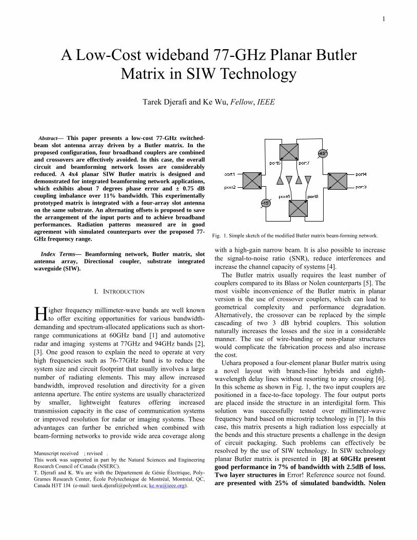
1
Abstract— This paper presents a low-cost 77-GHz switched-beam slot antenna array driven by a Butler matrix. In the proposed configuration, four broadband couplers are combined and crossovers are effectively avoided. In this case, the overall circuit and beamforming network losses are considerably reduced. A 4x4 planar SIW Butler matrix is designed and demonstrated for integrated beamforming network applications, which exhibits about 7 degrees phase error and ± 0.75 dB coupling imbalance over 11% bandwidth. This experimentally prototyped matrix is integrated with a four-array slot antenna on the same substrate. An alternating offsets is proposed to save the arrangement of the input ports and to achieve broadband performances. Radiation patterns measured are in good agreement with simulated counterparts over the proposed 77-GHz frequency range.
Index Terms— Beamforming network, Butler matrix, slot antenna array, Directional coupler, substrate integrated waveguide (SIW).
I. INTRODUCTION
igher frequency millimeter-wave bands are well known to offer exciting opportunities for various bandwidth-
demanding and spectrum-allocated applications such as short-range communications at 60GHz band [1] and automotive radar and imaging systems at 77GHz and 94GHz bands [2], [3]. One good reason to explain the need to operate at very high frequencies such as 76-77GHz band is to reduce the system size and circuit footprint that usually involves a large number of radiating elements. This may allow increased bandwidth, improved resolution and directivity for a given antenna aperture. The entire systems are usually characterized by smaller, lightweight features offering increased transmission capacity in the case of communication systems or improved resolution for radar or imaging systems. These advantages can further be enriched when combined with beam-forming networks to provide wide area coverage along
Manuscript received ; revised . This work was supported in part by the Natural Sciences and Engineering Research Council of Canada (NSERC). T. Djerafi and K. Wu are with the Département de Génie Électrique, Poly-Grames Research Center, École Polytechnique de Montréal, Montréal, QC, Canada H3T 1J4 (e-mail: [email protected]; [email protected]).
with a high-gain narrow beam. It is also possible to increase the signal-to-noise ratio (SNR), reduce interferences and increase the channel capacity of systems [4].
The Butler matrix usually requires the least number of couplers compared to its Blass or Nolen counterparts [5]. The most visible inconvenience of the Butler matrix in planar version is the use of crossover couplers, which can lead to geometrical complexity and performance degradation. Alternatively, the crossover can be replaced by the simple cascading of two 3 dB hybrid couplers. This solution naturally increases the losses and the size in a considerable manner. The use of wire-banding or non-planar structures would complicate the fabrication process and also increase the cost.
Uehara proposed a four-element planar Butler matrix using a novel layout with branch-line hybrids and eighth-wavelength delay lines without resorting to any crossing [6]. In this scheme as shown in Fig. 1, the two input couplers are positioned in a face-to-face topology. The four output ports are placed inside the structure in an interdigital form. This solution was successfully tested over millimeter-wave frequency band based on microstrip technology in [7]. In this case, this matrix presents a high radiation loss especially at the bends and this structure presents a challenge in the design of circuit packaging. Such problems can effectively be resolved by the use of SIW technology. In SIW technology planar Butler matrix is presented in [8] at 60GHz present good performance in 7% of bandwidth with 2.5dB of loss. Two layer structures in Error! Reference source not found. are presented with 25% of simulated bandwidth. Nolen
A Low-Cost wideband 77-GHz Planar Butler Matrix in SIW Technology
Tarek Djerafi and Ke Wu, Fellow, IEEE
H
Fig. 1. Simple sketch of the modified Butler matrix beam-forming network.

2
matrix which is special case of the butler matrix is studied in [10].
A new SIW planar 4x4 Butler matrix without using any crossovers is presented in this paper. Narrow-wall SIW couplers with no mitred H-plane waveguide bends are designed as fundamental building blocks for the proposed matrix structure. The whole matrix is designed and simulated with HFSS. This structure is used to feed a 4x4 slot antenna array, and its measured radiation patterns are in good agreement with simulated results based on array factors. The SIW slot antenna fed by the Butler matrix developed in this work provides a cost-effective approach to implementing an adaptive antenna for 77GHz radar applications as well as other millimetre-wave systems such as 60GHz wireless communications.
II. BUTLER DESIGN
The proposed Butler matrix consists of hybrids coupler and phase shifters without crossovers involved in the structure. To ensure wideband performances of the Butler matrix, wideband components must be designed. In this work, a compact Riblet short slot directional coupler is used that has such features as equal power splitting, high isolation and accurate 90 degree phasing [11].
A. SIW Hybrid Coupler
In this work, a continuous aperture coupling scheme is adopted. The coupling section consists of one continuous aperture with length 1L . The phase difference between the two
modes is:
1 1
ge go
2L L
. (1)
λge and λgo are the even- and odd-mode wavelengths in substrate. A substrate RT/duroïd 6002 is used with 20mil thickness and the nominal loss tangent of the substrate about 0.0012(gives by the fabricant). To obtain φ=90 degree at 77 GHz 1L should be equal to 1.8 mm. The width of the
coupling region must be reduced to prevent the undesired TE30 mode from propagation. The H-plane impedance step is
used to achieve the matching condition. Different bends are added to adjust the coupler to the input and output port positions within the proposed matrix topology, which in fact yields two coupler versions as illustrated in Fig. 2. The hybrid coupler is designed to operate from 72 GHz to 81 GHz. The design is then optimized with HFSS. Different dimensions of the designed couplers are detailed in Table 1.
Fig. 3 shows simulated results of the proposed coupler. Over the frequency band of our interest, simulated transmission coefficients at port 2 and port 3 are well equalized around 3.2 dB. The loss is estimated around 0.2dB for the designed couplers and is principally caused by the dielectric loss. The isolation and return loss are better than 20dB over the desired frequency band. The relative phase difference of output and coupled ports is 90 degrees across the frequency band of 72-81 GHz. These results clearly demonstrate an excellent quadrature coupling property.
B. Butler Matrix
Four planar hybrid couplers and H-plane bends are connected by SIW waveguide of different lengths to build a planar eight port structure. A length of waveguide at the centre
Fig. 2. Narrow wall coupler with different bends.
Fig. 3. Simulated S-parameters for 3 dB SIW couplers.
Fig. 4. SIW Butler matrix scheme without crossover.
TABLE I: H-PLANE COUPLERS PARAMETERS (mm) a L1 L2 s w
1.758 2.294 1.085 0.248 3.05
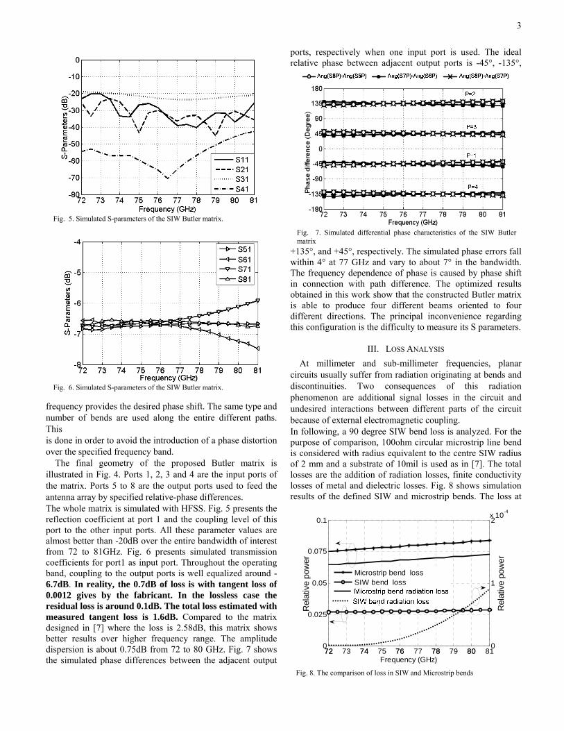
3
frequency provides the desired phase shift. The same type and number of bends are used along the entire different paths. This is done in order to avoid the introduction of a phase distortion over the specified frequency band.
The final geometry of the proposed Butler matrix is illustrated in Fig. 4. Ports 1, 2, 3 and 4 are the input ports of the matrix. Ports 5 to 8 are the output ports used to feed the antenna array by specified relative-phase differences. The whole matrix is simulated with HFSS. Fig. 5 presents the reflection coefficient at port 1 and the coupling level of this port to the other input ports. All these parameter values are almost better than -20dB over the entire bandwidth of interest from 72 to 81GHz. Fig. 6 presents simulated transmission coefficients for port1 as input port. Throughout the operating band, coupling to the output ports is well equalized around -6.7dB. In reality, the 0.7dB of loss is with tangent loss of 0.0012 gives by the fabricant. In the lossless case the residual loss is around 0.1dB. The total loss estimated with measured tangent loss is 1.6dB. Compared to the matrix designed in [7] where the loss is 2.58dB, this matrix shows better results over higher frequency range. The amplitude dispersion is about 0.75dB from 72 to 80 GHz. Fig. 7 shows the simulated phase differences between the adjacent output
ports, respectively when one input port is used. The ideal relative phase between adjacent output ports is -45°, -135°,
+135°, and +45°, respectively. The simulated phase errors fall within 4° at 77 GHz and vary to about 7° in the bandwidth. The frequency dependence of phase is caused by phase shift in connection with path difference. The optimized results obtained in this work show that the constructed Butler matrix is able to produce four different beams oriented to four different directions. The principal inconvenience regarding this configuration is the difficulty to measure its S parameters.
III. LOSS ANALYSIS
At millimeter and sub-millimeter frequencies, planar circuits usually suffer from radiation originating at bends and discontinuities. Two consequences of this radiation phenomenon are additional signal losses in the circuit and undesired interactions between different parts of the circuit because of external electromagnetic coupling. In following, a 90 degree SIW bend loss is analyzed. For the purpose of comparison, 100ohm circular microstrip line bend is considered with radius equivalent to the centre SIW radius of 2 mm and a substrate of 10mil is used as in [7]. The total losses are the addition of radiation losses, finite conductivity losses of metal and dielectric losses. Fig. 8 shows simulation results of the defined SIW and microstrip bends. The loss at
Fig. 7. Simulated differential phase characteristics of the SIW Butler matrix
Fig. 5. Simulated S-parameters of the SIW Butler matrix.
Fig. 6. Simulated S-parameters of the SIW Butler matrix.
72 73 74 75 76 77 78 79 80 810
0.025
0.05
0.075
0.1
Rel
ativ
e po
wer
72 74 76 78 800
1
2x 10⁻⁴
Frequency (GHz)
Rel
ativ
e po
wer
Microstrip bend radiation loss
Microstrip bend lossSIW bend lossSIW bend radiation loss
Fig. 8. The comparison of loss in SIW and Microstrip bends
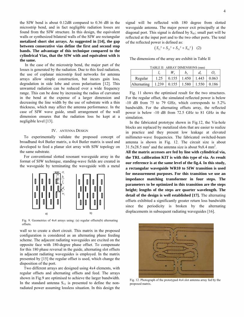
4
the SIW bend is about 0.12dB compared to 0.36 dB in the microstrip bend, and in fact negligible radiation losses are found from the SIW structure. In this design, the equivalent walls or synthesized bilateral walls of the SIW are rectangular metalized short slot arrays. As suggested in [14], the gap between consecutive vias define the first and second stop bands. The advantage of this technique compared to the cylindrical Vias, that the SIW with and equivalent with is the same.
In the case of the microstrip bend, the major part of the losses is generated by the radiation. Due to this feed radiation, the use of coplanar microstrip feed networks for antenna arrays allow simple construction, but incurs gain loss, degradation in side lobe and cross polarisation [12]. This unwanted radiation can be reduced over a wide frequency range. This can be done by increasing the radius of curvature in the bend at the expense of a larger dimension and decreasing the line width by the use of substrate with a thin thickness, which may affect the antenna performance. In the case of SIW wave guide, small arrangement of the wall dimension ensures that the radiation loss be kept at a negligible level [13].
IV. ANTENNA DESIGN
To experimentally validate the proposed concept of broadband 4x4 Butler matrix, a 4x4 Butler matrix is used and developed to feed a planar slot array with SIW topology on the same substrate.
For conventional slotted resonant waveguide array in the format of SIW technique, standing-wave fields are created in the waveguide by terminating the waveguide with a metal
wall so to create a short circuit. This matrix in the proposed configuration is considered as an alternating phase feeding scheme. The adjacent radiating waveguides are excited on the opposite face with 180-degree phase offset. To compensate for this 180 phase reversal in the guide, alternating slot offsets in adjacent radiating waveguides is employed. In the matrix presented by [15] the regular offset is used, which change the disposition of the port.
Two different arrays are designed using 4x4 elements, with regular offsets and alternating offsets and feed. The arrays shown in Fig.9 are optimised to achieve the larger bandwidth. In the standard antenna S11 is presented to define the non-radiated power assuming lossless situation. In this design the
signal will be reflected with 180 degree from slotted waveguide antenna. The major power exit principally at the diagonal port. This signal is defined by S41; small part will be reflected at the input port and to the two other ports. The total of the reflected power is defined as:
2 2 2 211 21 31 41S S S S (2)
The dimensions of the array are exhibit in Table II
Fig. 11 shows the optimised result for the two structures.
For the regular offset, the simulated reflected power is below -10 dB from 75 to 79 GHz, which corresponds to 5.2% bandwidth. For the alternating offsets array, the reflected power is below -10 dB from 72.5 GHz to 81 GHz in the simulation.
In the fabricated prototype shown in Fig.12, the Via-hole blocks are replaced by metalized slots that are easier to realize in practice and they present low leakage at elevated millimeter-wave frequencies. The fabricated switched-beam antenna is shown in Fig. 12. The circuit size is about 31.5x28.5 mm2 and the antenna size is about 9x8.4 mm2. All the matrix accesses are fed by line with cylindrical via, the TRL calibration KIT is with this type of via. As result our reference is at the same level of the fig.4. In this study, a rectangular waveguide WR10 to SIW transition is used for measurement purposes. For this transition we use an impedance matching transformer in four steps. The parameters to be optimized in this transition are the steps height; lengths of the steps are quarter wavelength. The detail of the design is well established [17]. The alternating offsets exhibited a significantly greater return loss bandwidth since the periodicity is broken by the alternating displacements in subsequent radiating waveguides [16].
TABLE II: ARRAY DIMENSIONS (mm)
ls Ws bs ds Os
Regular 1.25 0.155 1.450 1.443 0.063
Alternating 1.239 0.155 1.580 1.550 0.186
a) b)
sl
sw
sO
sb
sd
Fig. 9. Geometries of 4x4 arrays using: (a) regular offsets(b) alternating offsets.
Fig. 12. Photograph of the prototyped 4x4 slot antenna array fed by the proposed matrix.
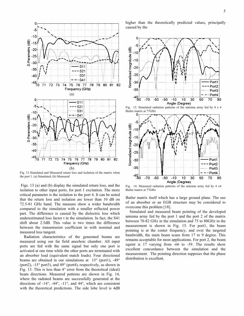
5
(a)
(b)
Fig. 13 Simulated and Measured return loss and isolation of the matrix when the port 1. (a) Simulated, (b) Measured
Figs. 13 (a) and (b) display the simulated return loss, and the isolation to other input ports, for port 1 excitation. The more critical parameter is the isolation to the port 4. It can be noted that the return loss and isolation are lower than 10 dB on 72.5-81 GHz band. The measure show a wider bandwidth compared to the simulation with a smaller reflected power part. The difference is caused by the dielectric loss which underestimated loss factor t in the simulation. In fact, the S41 shift about 2.5dB. This value is two times the difference between the transmission coefficient in with nominal and measured loss tangent.
Radiation characteristics of the generated beams are measured using our far field anechoic chamber. All input ports are fed with the same signal but only one port is activated at one time while the other ports are terminated with an absorber load (equivalent match loads). Four directional beams are obtained in our simulations at 15° (port1), -49° (port2), -15° port3), and 49° (port4), respectively, as shown in Fig. 13. This is less than 4° error from the theoretical (ideal) beam directions. Measured patterns are shown in Fig. 14, where the radiated beams are successfully generated at the directions of -14°, -44°, -11°, and 44°, which are consistent with the theoretical predictions. The side lobe level is 4dB
higher than the theoretically predicted values, principally caused by the
Butler matrix itself which has a large ground plane. The use of an absorber or an EGB structure may be considered to overcome this problem [18].
Simulated and measured beam pointing of the developed antenna array fed by the port 1 and the port 2 of the matrix between 70-82 GHz in the simulation and 75 to 80GHz in the measurement is shown in Fig. 15. For port1, the beam pointing is at the center frequency, and over the targeted bandwidth, the main beam scans from 17 to 9 degree. This remains acceptable for most applications. For port 2, the beam squint is 17 varying from -66 to -39. The results show excellent concordance between the simulation and the measurement. The pointing direction supposes that the phase distribution is excellent.
Fig. 13. Simulated radiation patterns of the antenna array fed by 4 x 4 Butler matrix at 77GHz
Fig. 14. Measured radiation patterns of the antenna array fed by 4 x4 Butler matrix at 77GHz
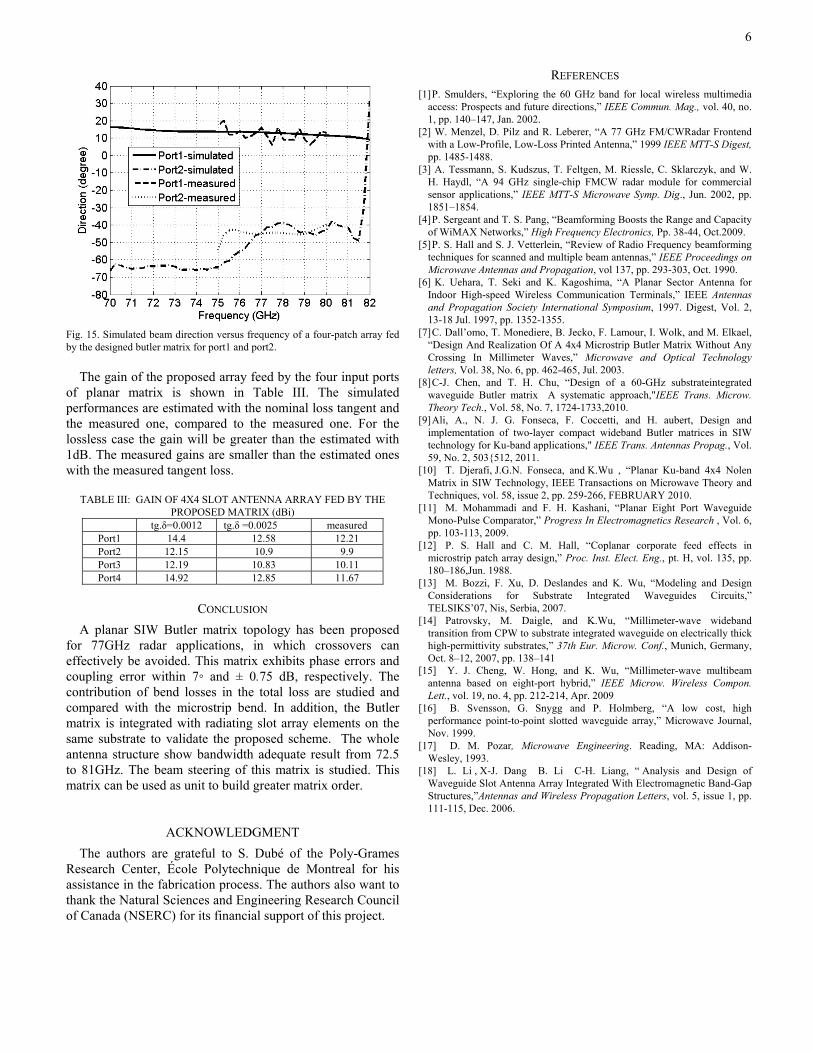
6
Fig. 15. Simulated beam direction versus frequency of a four-patch array fed by the designed butler matrix for port1 and port2.
The gain of the proposed array feed by the four input ports
of planar matrix is shown in Table III. The simulated performances are estimated with the nominal loss tangent and the measured one, compared to the measured one. For the lossless case the gain will be greater than the estimated with 1dB. The measured gains are smaller than the estimated ones with the measured tangent loss.
TABLE III: GAIN OF 4X4 SLOT ANTENNA ARRAY FED BY THE
PROPOSED MATRIX (dBi) tg.δ=0.0012 tg.δ =0.0025 measured
Port1 14.4 12.58 12.21 Port2 12.15 10.9 9.9 Port3 12.19 10.83 10.11 Port4 14.92 12.85 11.67
CONCLUSION
A planar SIW Butler matrix topology has been proposed for 77GHz radar applications, in which crossovers can effectively be avoided. This matrix exhibits phase errors and coupling error within 7◦ and ± 0.75 dB, respectively. The contribution of bend losses in the total loss are studied and compared with the microstrip bend. In addition, the Butler matrix is integrated with radiating slot array elements on the same substrate to validate the proposed scheme. The whole antenna structure show bandwidth adequate result from 72.5 to 81GHz. The beam steering of this matrix is studied. This matrix can be used as unit to build greater matrix order.
ACKNOWLEDGMENT
The authors are grateful to S. Dubé of the Poly-Grames Research Center, École Polytechnique de Montreal for his assistance in the fabrication process. The authors also want to thank the Natural Sciences and Engineering Research Council of Canada (NSERC) for its financial support of this project.
REFERENCES [1] P. Smulders, “Exploring the 60 GHz band for local wireless multimedia
access: Prospects and future directions,” IEEE Commun. Mag., vol. 40, no. 1, pp. 140–147, Jan. 2002.
[2] W. Menzel, D. Pilz and R. Leberer, “A 77 GHz FM/CWRadar Frontend with a Low-Profile, Low-Loss Printed Antenna,” 1999 IEEE MTT-S Digest, pp. 1485-1488.
[3] A. Tessmann, S. Kudszus, T. Feltgen, M. Riessle, C. Sklarczyk, and W. H. Haydl, “A 94 GHz single-chip FMCW radar module for commercial sensor applications,” IEEE MTT-S Microwave Symp. Dig., Jun. 2002, pp. 1851–1854.
[4] P. Sergeant and T. S. Pang, “Beamforming Boosts the Range and Capacity of WiMAX Networks,” High Frequency Electronics, Pp. 38-44, Oct.2009.
[5] P. S. Hall and S. J. Vetterlein, “Review of Radio Frequency beamforming techniques for scanned and multiple beam antennas,” IEEE Proceedings on Microwave Antennas and Propagation, vol 137, pp. 293-303, Oct. 1990.
[6] K. Uehara, T. Seki and K. Kagoshima, “A Planar Sector Antenna for Indoor High-speed Wireless Communication Terminals,” IEEE Antennas and Propagation Society International Symposium, 1997. Digest, Vol. 2, 13-18 Jul. 1997, pp. 1352-1355.
[7] C. Dall’omo, T. Monediere, B. Jecko, F. Lamour, I. Wolk, and M. Elkael, “Design And Realization Of A 4x4 Microstrip Butler Matrix Without Any Crossing In Millimeter Waves,” Microwave and Optical Technology letters, Vol. 38, No. 6, pp. 462-465, Jul. 2003.
[8] C-J. Chen, and T. H. Chu, “Design of a 60-GHz substrateintegrated waveguide Butler matrix A systematic approach,"IEEE Trans. Microw. Theory Tech., Vol. 58, No. 7, 1724-1733,2010.
[9] Ali, A., N. J. G. Fonseca, F. Coccetti, and H. aubert, Design and implementation of two-layer compact wideband Butler matrices in SIW technology for Ku-band applications," IEEE Trans. Antennas Propag., Vol. 59, No. 2, 503{512, 2011.
[10] T. Djerafi, J.G.N. Fonseca, and K.Wu , “Planar Ku-band 4x4 Nolen Matrix in SIW Technology, IEEE Transactions on Microwave Theory and Techniques, vol. 58, issue 2, pp. 259-266, FEBRUARY 2010.
[11] M. Mohammadi and F. H. Kashani, “Planar Eight Port Waveguide Mono-Pulse Comparator,” Progress In Electromagnetics Research , Vol. 6, pp. 103-113, 2009.
[12] P. S. Hall and C. M. Hall, “Coplanar corporate feed effects in microstrip patch array design,” Proc. Inst. Elect. Eng., pt. H, vol. 135, pp. 180–186,Jun. 1988.
[13] M. Bozzi, F. Xu, D. Deslandes and K. Wu, “Modeling and Design Considerations for Substrate Integrated Waveguides Circuits,” TELSIKS’07, Nis, Serbia, 2007.
[14] Patrovsky, M. Daigle, and K.Wu, “Millimeter-wave wideband transition from CPW to substrate integrated waveguide on electrically thick high-permittivity substrates,” 37th Eur. Microw. Conf., Munich, Germany, Oct. 8–12, 2007, pp. 138–141
[15] Y. J. Cheng, W. Hong, and K. Wu, “Millimeter-wave multibeam antenna based on eight-port hybrid,” IEEE Microw. Wireless Compon. Lett., vol. 19, no. 4, pp. 212-214, Apr. 2009
[16] B. Svensson, G. Snygg and P. Holmberg, “A low cost, high performance point-to-point slotted waveguide array,” Microwave Journal, Nov. 1999.
[17] D. M. Pozar, Microwave Engineering. Reading, MA: Addison-Wesley, 1993.
[18] L. Li , X-J. Dang B. Li C-H. Liang, “ Analysis and Design of Waveguide Slot Antenna Array Integrated With Electromagnetic Band-Gap Structures,”Antennas and Wireless Propagation Letters, vol. 5, issue 1, pp. 111-115, Dec. 2006.

62
ARTICLE II: MULTI-LAYERED SUBSTRATE INTEGRATED
WAVEGUIDE BUTLER MATRIX FOR MILLIMETER-WAVE SYSTEM
APPLICATIONS
Tarek Djerafi, and Ke Wu, Fellow, IEEE
Soumis 18 mars 2010 IEEE Transactions on Antenna and Propagation.
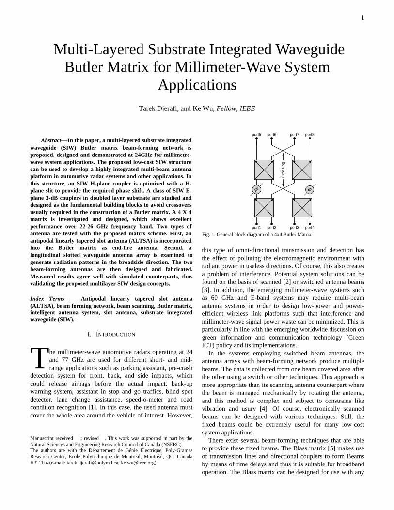
1
Abstract—In this paper, a multi-layered substrate integrated
waveguide (SIW) Butler matrix beam-forming network is
proposed, designed and demonstrated at 24GHz for millimetre-
wave system applications. The proposed low-cost SIW structure
can be used to develop a highly integrated multi-beam antenna
platform in automotive radar systems and other applications. In
this structure, an SIW H-plane coupler is optimized with a H-
plane slit to provide the required phase shift. A class of SIW E-
plane 3-dB couplers in doubled layer substrate are studied and
designed as the fundamental building blocks to avoid crossovers
usually required in the construction of a Butler matrix. A 4 X 4
matrix is investigated and designed, which shows excellent
performance over 22-26 GHz frequency band. Two types of
antenna are tested with the proposed matrix scheme. First, an
antipodal linearly tapered slot antenna (ALTSA) is incorporated
into the Butler matrix as end-fire antenna. Second, a
longitudinal slotted waveguide antenna array is examined to
generate radiation patterns in the broadside direction. The two
beam-forming antennas are then designed and fabricated.
Measured results agree well with simulated counterparts, thus
validating the proposed multilayer SIW design concepts.
Index Terms — Antipodal linearly tapered slot antenna
(ALTSA), beam forming network, beam scanning, Butler matrix,
intelligent antenna system, slot antenna, substrate integrated
waveguide (SIW).
I. INTRODUCTION
he millimeter-wave automotive radars operating at 24
and 77 GHz are used for different short- and mid-
range applications such as parking assistant, pre-crash
detection system for front, back, and side impacts, which
could release airbags before the actual impact, back-up
warning system, assistant in stop and go traffics, blind spot
detector, lane change assistance, speed-o-meter and road
condition recognition [1]. In this case, the used antenna must
cover the whole area around the vehicle of interest. However,
Manuscript received ; revised . This work was supported in part by the
Natural Sciences and Engineering Research Council of Canada (NSERC).
The authors are with the Département de Génie Électrique, Poly-Grames
Research Center, École Polytechnique de Montréal, Montréal, QC, Canada
H3T 1J4 (e-mail: [email protected]; [email protected]).
this type of omni-directional transmission and detection has
the effect of polluting the electromagnetic environment with
radiant power in useless directions. Of course, this also creates
a problem of interference. Potential system solutions can be
found on the basis of scanned [2] or switched antenna beams
[3]. In addition, the emerging millimeter-wave systems such
as 60 GHz and E-band systems may require multi-beam
antenna systems in order to design low-power and power-
efficient wireless link platforms such that interference and
millimeter-wave signal power waste can be minimized. This is
particularly in line with the emerging worldwide discussion on
green information and communication technology (Green
ICT) policy and its implementations.
In the systems employing switched beam antennas, the
antenna arrays with beam-forming network produce multiple
beams. The data is collected from one beam covered area after
the other using a switch or other techniques. This approach is
more appropriate than its scanning antenna counterpart where
the beam is managed mechanically by rotating the antenna,
and this method is complex and subject to constrains like
vibration and usury [4]. Of course, electronically scanned
beams can be designed with various techniques. Still, the
fixed beams could be extremely useful for many low-cost
system applications.
There exist several beam-forming techniques that are able
to provide these fixed beams. The Blass matrix [5] makes use
of transmission lines and directional couplers to form Beams
by means of time delays and thus it is suitable for broadband
operation. The Blass matrix can be designed for use with any
Multi-Layered Substrate Integrated Waveguide
Butler Matrix for Millimeter-Wave System
Applications
Tarek Djerafi, and Ke Wu, Fellow, IEEE
T
port1 port2 port3 port4
port5 port6 port7 port8
Cro
ssin
g
Fig. 1. General block diagram of a 4x4 Butler Matrix
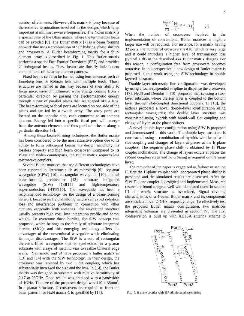
2
number of elements. However, this matrix is lossy because of
the resistive terminations involved in the design, which is an
important at millimetre-wave frequencies. The Nolen matrix is
a special case of the Blass matrix, where the termination loads
can be avoided [6]. The Butler matrix [7] is a beam forming
network that uses a combination of 90° hybrids, phase shifters
and crossovers. A Butler beamforming matrix for a four-
element array is described in Fig. 1. This Butler matrix
performs a spatial Fast Fourier Transform (FFT) and provides
2n orthogonal beams. These beams are linearly independent
combinations of the array element patterns.
Fixed beams can also be formed using lens antennas such as
Luneberg lens or Rotman lens with multiple feeds. Those
structures are named in this way because of their ability to
focus microwave or millimeter wave energy coming from a
particular direction by passing the electromagnetic energy
through a pair of parallel plates that are shaped like a lens.
The beam-forming or focal ports are located on one side of the
plates and are fed by a switch array. The array ports are
located on the opposite side, each connected to an antenna
element. Energy fed into a specific focal port will emerge
from the antenna elements and thus produce a beam along a
particular direction [8].
Among those beam-forming techniques, the Butler matrix
has been considered to be the most attractive option due to its
ability to form orthogonal beams, its design simplicity, its
lossless property and high beam crossover. Compared to its
Blass and Nolen counterparts, the Butler matrix requires less
microwave couplers.
Several Butler matrices that use different technologies have
been reported in literature such as microstrip [9], coplanar
waveguide (CPW) [10], rectangular waveguide [10], optical
beam-forming architecture [12], substrate integrated
waveguide (SIW) [13][14] and high-temperature
superconductors (HTS)[16]. The waveguide has been a
recommended technology for the design of a beam-forming
network because its field shielding nature can avoid radiation
loss and interference problems in connection with other
circuitry especially with antennas. The waveguide structure
usually presents high cost, low integration profile and heavy
weight. To overcome those hurdles, the SIW concept was
proposed, which belongs to the family of substrate integrated
circuits (SICs), and this emerging technology offers the
advantages of the conventional waveguide while eliminating
its major disadvantages. The SIW is a sort of rectangular
dielectric-filled waveguide that is synthesized in a planar
substrate with arrays of metallic vias to realize bilateral edge
walls. Yamamoto and al have proposed a butler matrix in
[13] and [14] with the SIW technology. In their design, the
crossover was replaced by two 3 dB couplers, which has
substantially increased the size and the loss. In [14], the Butler
matrix was designed in substrate with relative permittivity of
2.17 at 26GHz. Good results was obtained with a bandwidth
of 1GHz. The size of the proposed design was 110 x 35mm2.
In a planar structure, C crossovers are required to form the
beam pattern, for NxN matrix C is specified by [15]:
2log (N)
k 1
k 1
N2 1
2
(1)
When the number of crossovers involved in the
implementation of conventional Butler matrices is high, a
larger size will be required. For instance, for a matrix having
32 ports, the number of crossovers is 416, which is very large
and it could introduce a higher level of transmission loss
(typical 1 dB in the described 4x4 Butler matrix design). For
this reason, a configuration free from crossovers becomes
attractive. In this perspective, a new design of Butler matrix is
proposed in this work using the SIW technology in double
layered substrate.
Double-layer microstrip line configuration was developed
by using a foam-suspended stripline to dispense the crossovers
[17]. Nedil and Denidni in [10] proposed matrix using a two-
layer substrate, where the top layer is coupled to the bottom
layer through slot-coupled directional couplers. In [18], the
authors proposed a novel double-layer configuration using
rectangular waveguides; the double layer structure was
constructed using hybrids with broad-wall slot coupling and
change of layers at the phase shifters.
A novel double-layer configuration using SIW is proposed
and demonstrated in this work. The double-layer structure is
constructed using a combination of hybrids with broad-wall
slot coupling and changes of layers at places at the E plane
couplers. The required phase shift is obtained by H Plane
coupler inclinations. The change of layers occurs at places the
second couplers stage and no crossing is required on the same
layer.
The reminder of the paper is organized as fallow: in section
II, first the H-plane coupler with incorporated phase shifter is
presented and the simulated results are discussed. After the
SIW E-plane coupler is designed and implemented. Measured
results are found to agree well with simulated ones. In section
III the whole structure is assembled, Signal dividing
characteristics of a 4-beam Butler matrix and its components
are simulated over 24GHz frequency range. To effectively test
the proposed Butler matrix configuration, two matrices
integrating antennas are presented in section IV. The first
configuration is built up with ALTSA antenna scheme to
s
d
l2 l1
h
a
l3
α
Port1
Port2 Port3
Port4
Fig. 2. H plane coupler with 45° additional phase shifting
3
radiate in the end-fire direction. The second is constructed
built on the basis of a slotted waveguide array antenna for
broad side radiation. The proposed beam-forming networks
are designed, optimized, fabricated. Experiments are carried
out on these networks and measured results are presented and
compared with simulated results. Finally, Section V presents
our conclusions. Field-theoretical analysis is conducted using
HFSS for each component as well as the entire structure of the
network.
II. PROPOSED BUTLER MATRIX COMPONENTS
A. 135-Degree directional coupler
The H-plane rectangular waveguide is commonly used in
the design of microwave circuits and especially in the antenna
feeding systems. With the SIW technology, different
topologies have been proposed. A continuous aperture
coupling [19], for example, was applied in the design of SIW-
based couplers, or a multiple aperture technique was described
in [20] for the same purpose. In this design, the coupling
section consists of one continuous aperture L3 as shown in Fig.
2. The phase difference between the two modes is:
The phase differ 3 3
ge go
2L L
(2)
λge and λgo are the even and odd mode wavelength in substrate
waveguide. In our case, a RT/duroïd 6002 substrate is used
with 20mil thickness. At 24 GHz, to obtain a phase difference
of 90 degree, L3 should be 5.2mm. The width of the coupling
region must be reduced to prevent the undesired TE30 mode.
The H plane impudence step is used to achieve the matching.
To achieve an additional phase shifting to the initial 90
degree, an SIW line with different length must be added to the
direct and coupling ports. A slow wave structure can be used
also to meet the phase shift requirement as in [21]. In our
work, 3dB, 135° coupler designed for the Butler matrix is
shown in Fig. 2. The H-plane corner is used to provide a 45-
degree additional phase shifting between the output- and
coupled ports. The advantage is that the coupler is small in
size. And also, different ports in this configuration are
separated to facilitate the access and measurements.
Usually, the symmetrical H-plane bend angle varies
between 20 and 90 degrees. The corner of a waveguide edge
can be shaped circularly, but in most designs, bend has shard
edge. For non-mitred H-plane waveguide, structure bends
have been analysed and their equivalent circuits have been
documented in Marcuvitz’s landmark waveguide handbook
[22].
The design is optimized with HFSS software package;
Different dimensions of the designed coupler with inclination
are detailed in Table 1.
Simulated S-parameters results are shown in Fig .3. The
isolation and the return losses are below -20dB over the
frequency range of 21.8-28GHz. The ±0.5 dB power equality
bandwidth covers 21-26 GHz.
Fig. 4 presents a relative difference of the simulated phases
regarding output- and coupled ports. As shown in this figure,
the simulated relative phase difference with ±5 degrees is
detailed across the frequency band of 22-25 GHz and ±10
degrees over all the simulated bandwidth.
B. Compact E- plane coupler
Hadge proposed a compact hybrid using two lateral slots on
the common wall of two waveguides as shown in Fig. 5 [24].
The performance of this broad-wall directional coupler is
nearly identical to that of a narrow coupler with the same slot
dimensions.
As shown in Fig. 5, two slots of the same dimension are cut
on the common broad-wall of the two waveguides. The slots
are located adjacent to the boundary side-wall of the
waveguide, equidistant from the guide center-line, opposite
TABLE I: H-PLAN COUPLER WITH 45° ADDITIONAL PHASE
SHIFTING PARAMETERS
a 5.67mm
h 0.92mm
L1 2.8mm
L2 7.8mm
L3 5.4mm
d 0.8mm
s 1.6mm
α 14.7 degree
Fig. 3. Simulated S parameters result.
Fig. 4. Simulated curves for relative phase difference between output and
coupled ports.
4
from each other, and in a longitudinal position.
The design of such component is based on Bethe’s theory
of diffraction by small holes [25][26]. To account for the large
apertures, different correction terms in the polarizability have
been developed [26]. Assuming monomode propagation in the
rectangular waveguide, the coupling can be caused by field
components Hx represented by [27] a series reactance, a
susceptance for coupling by Hz and a shunt susceptance for
coupling by Ey. The values of these lumped elements are
function of magnetic and electric polarizability functions Pm,e :
,
, ,
,
tan2
2
cm e
m e m e Slot
cm e
f
fP R l
f
f
(3)
fcm,e is the aperture resonance frequency given by the
respective cutoff frequencies of waveguide identical cross-
section. Rm,e are dimensionless quantities associated with the
TE10 mode and TM11 mode fields. These term are function of
a rectangular aperture of large lSlot and width wSlot .
In the presence of waveguide thickness t, this term is
multiplied by Ate , is the attenuation constant and A is
correction factor. To improve the performance, smooth tapers
were introduced along both the broad and narrow walls of this
structure and the ends of the slots. This modification is to
minimize the effect of metallic wall thickness. The proposed
structures based on the SIW technique have the obvious
advantage that the conductor is just a printed sheet which
reduces its effect. Thus, broad-wall couplers can be used to
obtain various power coupling levels through various designs
of coupler. A change in broad-wall slot displacement yields
different power coupling and requires an adjustment of slot
dimensions to achieve the same directional coupler
performance.
With the SIW technologies, a number of highly integrated
components have been developed on the basis of a E-plane
slot configuration including numerous filters, and of course
directional couplers were studied theoretically [23]. However,
no fabricated microwave coupler components have been
presented to date with satisfactory results. The problem is the
limitation in the fabrication of double layers PCB, especially
for the metalized holes connection to the middle ground of the
assembly, and for the air gap between the layers. The coupler
consists of two PCBs glued together, the air gap between the
two PCBs constitute parallel plate waveguide, A part of the
coupled power travels on this TEM line which supports no
desired higher order modes. To resolve this problem, the two
common conductor plans must be avoided in the slot region.
Slot length LSlot and slot width wSlot are designed to obtain
3dB coupling with 90-degree difference in the two output
ports while suppressing reflection to the two input ports. In
this work, this coupler is constructed with a double-layer
dielectric substrate having dielectric constant of 2.96 and
height of 0.508 mm. The initial value of wSlot is equal to
substrate thickness hsub, and with the explained method, the
calculated value LSlot is 9mm.
Fig. 6 illustrates the deployment of two slots on the
common plane between the primary and secondary SIWs. The
microwave signal is injected from port 1 (input port) of the
primary SIW, part of the energy propagates forward directly
and then outputs from port 2 (the through port) of the primary
waveguide, while the remaining energy is coupled to the
secondary waveguide and comes out of port 3 (coupled port),
and port 4 is the isolated port. A microstrip taper with widths
w, wt and length lt is adopted to match the microstrip line and
SIW over a wideband [28].
Por
t1
Por
t4
Por
t3
Por
t2
Fig. 6. SIW broad-wall directional coupler.
Fig. 7. Measured and simulated return loss and isolation.
xzylSlot
wSlot
Fig. 5. Broad wall coupler.
TABLE II: BROAD-WALL DIRECTIONAL COUPLER
PARAMETERS
w 1.33mm
wt 2.30mm
lt 2.65mm
LSlot 8.95mm
wSlot 0.48mm
5
A 3dB coupler structure is optimized with HFSS package
and then fabricated. The optimized dimensions are specified in
Table II.
The return loss and isolation are in excess of 20 dB over a
bandwidth of 28.6%, as illustrated in Fig.7. The return loss is
lower than -10dB over the measured band.
It can be seen in Fig.8 that the outputs at ports 2 and 3 are
ranged from 3.2 dB to 4dB in the bandwidth of 22 to 26 GHz.
The increase of insertion loss is caused by the SIW-microstrip
transitions and dielectric loss.
Fig. 9 presents measured and simulated relative phases of
S21 and S31. As shown in the figure, the measured relative
phase is within 3 degree of the required 90 degree across the
entire frequency band of 22–26 GHz. Probably, this phase
offset may originate from the effect of the transition and the
test fixture. A close comparison is made between
measurements and simulations.
III. 4 X 4 BUTLER MATRIX
Combining the above-presented components, the entire Butler
matrix circuit is designed with the two-layer substrate. The top
layer is coupled to the bottom layer through the slot-
directional couplers. The general scheme is illustrated in Fig.
10. It can be seen that a signal incident at input port
(#1,#2,#,#4) is divided into four outputs #5,#6,#7 and #8 with
adequate amplitude and phase.
Generally 45 degree is used as phase shift between two
couplers sections of the Butler matrix. In this configuration,
135 degree phase shift is used. This modification is imposed
by the fabrication process limit in our laboratory. The phase
shift between two adjacent output ports when the port
(#1,#2,#,#4) is used are -135,45,-45,135 respectively, which
correspond respectively to (2L, 1R, 1L, 2R) radiation pattern
direction. The matrix is simulated using HFSS over the 20-28
GHz frequency band. Fig. 11 (a) and (b) display the
Fig. 8. - Measured and simulated coupled and transmitted power.
Fig. 9. Measured and simulated phase shifts between the outputs of coupler.
(a)
(b)
Fig. 11. Simulated results of the 4 x 4 Butler matrix. (a) Signal at port 1.(b)
Signal at port 2
Port#1 Port#2 Port#3Port#4
Port#8
Port#7Port#6
Port#5
Fig. 10. Butler matrix scheme on a two-layer SIW structure.
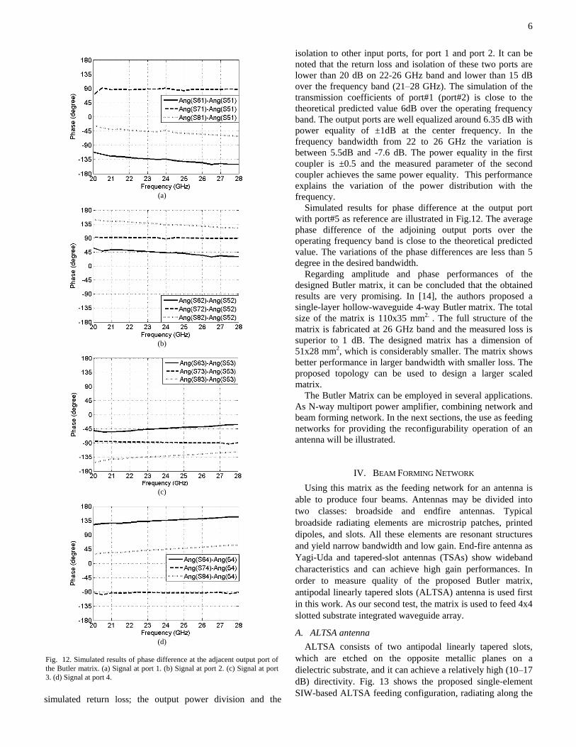
6
simulated return loss; the output power division and the
isolation to other input ports, for port 1 and port 2. It can be
noted that the return loss and isolation of these two ports are
lower than 20 dB on 22-26 GHz band and lower than 15 dB
over the frequency band (21–28 GHz). The simulation of the
transmission coefficients of port#1 (port#2) is close to the
theoretical predicted value 6dB over the operating frequency
band. The output ports are well equalized around 6.35 dB with
power equality of ±1dB at the center frequency. In the
frequency bandwidth from 22 to 26 GHz the variation is
between 5.5dB and -7.6 dB. The power equality in the first
coupler is ±0.5 and the measured parameter of the second
coupler achieves the same power equality. This performance
explains the variation of the power distribution with the
frequency.
Simulated results for phase difference at the output port
with port#5 as reference are illustrated in Fig.12. The average
phase difference of the adjoining output ports over the
operating frequency band is close to the theoretical predicted
value. The variations of the phase differences are less than 5
degree in the desired bandwidth.
Regarding amplitude and phase performances of the
designed Butler matrix, it can be concluded that the obtained
results are very promising. In [14], the authors proposed a
single-layer hollow-waveguide 4-way Butler matrix. The total
size of the matrix is 110x35 mm2. . The full structure of the
matrix is fabricated at 26 GHz band and the measured loss is
superior to 1 dB. The designed matrix has a dimension of
51x28 mm2, which is considerably smaller. The matrix shows
better performance in larger bandwidth with smaller loss. The
proposed topology can be used to design a larger scaled
matrix.
The Butler Matrix can be employed in several applications.
As N-way multiport power amplifier, combining network and
beam forming network. In the next sections, the use as feeding
networks for providing the reconfigurability operation of an
antenna will be illustrated.
IV. BEAM FORMING NETWORK
Using this matrix as the feeding network for an antenna is
able to produce four beams. Antennas may be divided into
two classes: broadside and endfire antennas. Typical
broadside radiating elements are microstrip patches, printed
dipoles, and slots. All these elements are resonant structures
and yield narrow bandwidth and low gain. End-fire antenna as
Yagi-Uda and tapered-slot antennas (TSAs) show wideband
characteristics and can achieve high gain performances. In
order to measure quality of the proposed Butler matrix,
antipodal linearly tapered slots (ALTSA) antenna is used first
in this work. As our second test, the matrix is used to feed 4x4
slotted substrate integrated waveguide array.
A. ALTSA antenna
ALTSA consists of two antipodal linearly tapered slots,
which are etched on the opposite metallic planes on a
dielectric substrate, and it can achieve a relatively high (10–17
dB) directivity. Fig. 13 shows the proposed single-element
SIW-based ALTSA feeding configuration, radiating along the
(a)
(b)
(c)
(d)
Fig. 12. Simulated results of phase difference at the adjacent output port of
the Butler matrix. (a) Signal at port 1. (b) Signal at port 2. (c) Signal at port
3. (d) Signal at port 4.
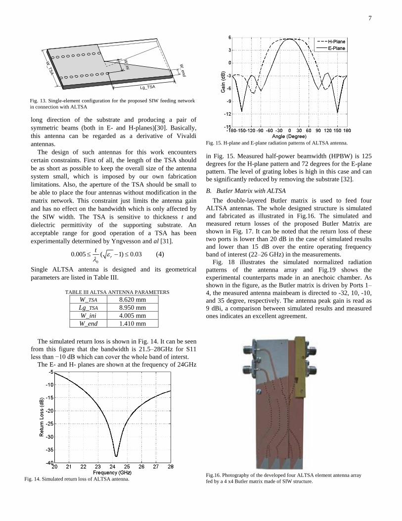
7
long direction of the substrate and producing a pair of
symmetric beams (both in E- and H-planes)[30]. Basically,
this antenna can be regarded as a derivative of Vivaldi
antennas.
The design of such antennas for this work encounters
certain constraints. First of all, the length of the TSA should
be as short as possible to keep the overall size of the antenna
system small, which is imposed by our own fabrication
limitations. Also, the aperture of the TSA should be small to
be able to place the four antennas without modification in the
matrix network. This constraint just limits the antenna gain
and has no effect on the bandwidth which is only affected by
the SIW width. The TSA is sensitive to thickness t and
dielectric permittivity of the supporting substrate. An
acceptable range for good operation of a TSA has been
experimentally determined by Yngvesson and al [31].
0
0.005 ( 1) 0.03r
t
(4)
Single ALTSA antenna is designed and its geometrical
parameters are listed in Table III.
The simulated return loss is shown in Fig. 14. It can be seen
from this figure that the bandwidth is 21.5–28GHz for S11
less than −10 dB which can cover the whole band of interst.
The E- and H- planes are shown at the frequency of 24GHz
in Fig. 15. Measured half-power beamwidth (HPBW) is 125
degrees for the H-plane pattern and 72 degrees for the E-plane
pattern. The level of grating lobes is high in this case and can
be significantly reduced by removing the substrate [32].
B. Butler Matrix with ALTSA
The double-layered Butler matrix is used to feed four
ALTSA antennas. The whole designed structure is simulated
and fabricated as illustrated in Fig.16. The simulated and
measured return losses of the proposed Butler Matrix are
shown in Fig. 17. It can be noted that the return loss of these
two ports is lower than 20 dB in the case of simulated results
and lower than 15 dB over the entire operating frequency
band of interest (22–26 GHz) in the measurements.
Fig. 18 illustrates the simulated normalized radiation
patterns of the antenna array and Fig.19 shows the
experimental counterparts made in an anechoic chamber. As
shown in the figure, as the Butler matrix is driven by Ports 1–
4, the measured antenna mainbeam is directed to -32, 10, -10,
and 35 degree, respectively. The antenna peak gain is read as
9 dBi, a comparison between simulated results and measured
ones indicates an excellent agreement.
Fig. 15. H-plane and E-plane radiation patterns of ALTSA antenna.
W_T
SA
Lg_TSA
W_end
W_in
i
Fig. 13. Single-element configuration for the proposed SIW feeding network
in connection with ALTSA
Fig.16. Photography of the developed four ALTSA element antenna array
fed by a 4 x4 Butler matrix made of SIW structure.
TABLE III ALTSA ANTENNA PARAMETERS
W_TSA 8.620 mm
Lg_TSA 8.950 mm
W_ini 4.005 mm
W_end 1.410 mm
Fig. 14. Simulated return loss of ALTSA antenna.
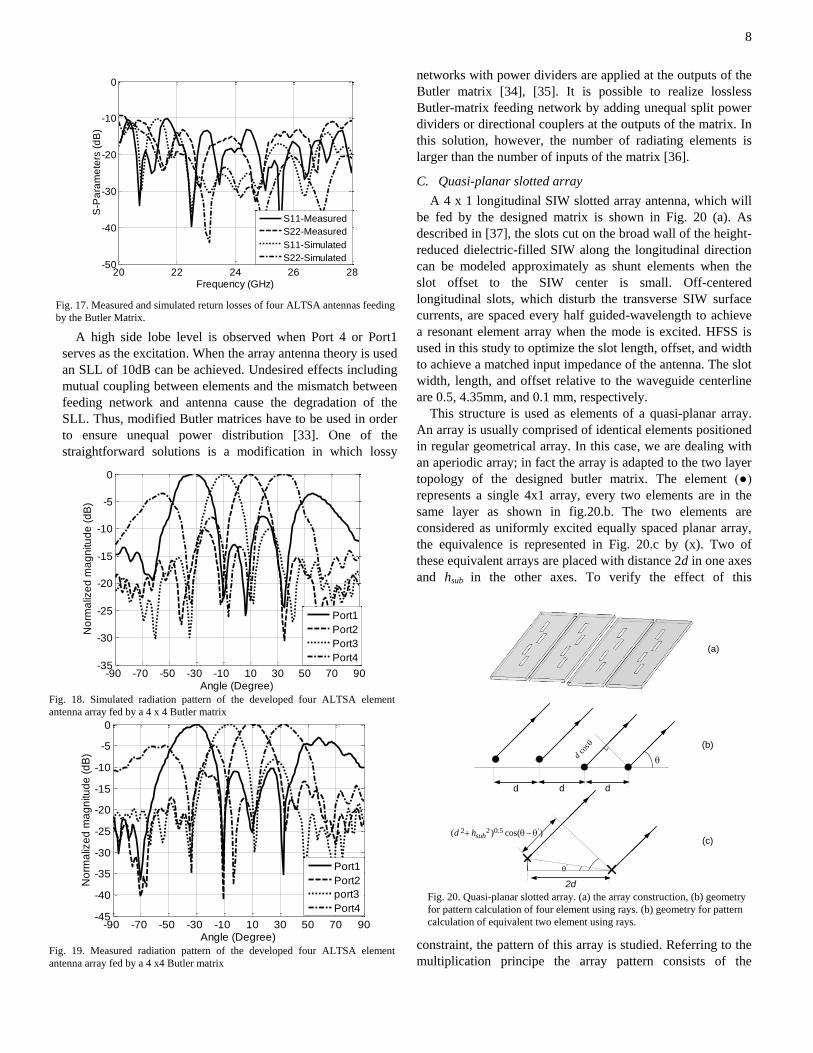
8
A high side lobe level is observed when Port 4 or Port1
serves as the excitation. When the array antenna theory is used
an SLL of 10dB can be achieved. Undesired effects including
mutual coupling between elements and the mismatch between
feeding network and antenna cause the degradation of the
SLL. Thus, modified Butler matrices have to be used in order
to ensure unequal power distribution [33]. One of the
straightforward solutions is a modification in which lossy
networks with power dividers are applied at the outputs of the
Butler matrix [34], [35]. It is possible to realize lossless
Butler-matrix feeding network by adding unequal split power
dividers or directional couplers at the outputs of the matrix. In
this solution, however, the number of radiating elements is
larger than the number of inputs of the matrix [36].
C. Quasi-planar slotted array
A 4 x 1 longitudinal SIW slotted array antenna, which will
be fed by the designed matrix is shown in Fig. 20 (a). As
described in [37], the slots cut on the broad wall of the height-
reduced dielectric-filled SIW along the longitudinal direction
can be modeled approximately as shunt elements when the
slot offset to the SIW center is small. Off-centered
longitudinal slots, which disturb the transverse SIW surface
currents, are spaced every half guided-wavelength to achieve
a resonant element array when the mode is excited. HFSS is
used in this study to optimize the slot length, offset, and width
to achieve a matched input impedance of the antenna. The slot
width, length, and offset relative to the waveguide centerline
are 0.5, 4.35mm, and 0.1 mm, respectively.
This structure is used as elements of a quasi-planar array.
An array is usually comprised of identical elements positioned
in regular geometrical array. In this case, we are dealing with
an aperiodic array; in fact the array is adapted to the two layer
topology of the designed butler matrix. The element (●)
represents a single 4x1 array, every two elements are in the
same layer as shown in fig.20.b. The two elements are
considered as uniformly excited equally spaced planar array,
the equivalence is represented in Fig. 20.c by (x). Two of
these equivalent arrays are placed with distance 2d in one axes
and hsub in the other axes. To verify the effect of this
constraint, the pattern of this array is studied. Referring to the
multiplication principe the array pattern consists of the
20 22 24 26 28-50
-40
-30
-20
-10
0
Frequency (GHz)
S-P
ara
me
ters
(d
B)
S11-Measured
S22-Measured
S11-Simulated
S22-Simulated
Fig. 17. Measured and simulated return losses of four ALTSA antennas feeding
by the Butler Matrix.
-90 -70 -50 -30 -10 10 30 50 70 90-35
-30
-25
-20
-15
-10
-5
0
Angle (Degree)
No
rma
lize
d m
ag
nitu
de
(d
B)
Port1
Port2
Port3
Port4
Fig. 18. Simulated radiation pattern of the developed four ALTSA element
antenna array fed by a 4 x 4 Butler matrix
-90 -70 -50 -30 -10 10 30 50 70 90-45
-40
-35
-30
-25
-20
-15
-10
-5
0
Angle (Degree)
No
rma
lize
d m
ag
nitu
de
(d
B)
Port1
Port2
port3
Port4
Fig. 19. Measured radiation pattern of the developed four ALTSA element
antenna array fed by a 4 x4 Butler matrix
d d d
'
2d
cos
d
2 2 0.5 '( ) cos( )subd h
(a)
(c)
(b)
Fig. 20. Quasi-planar slotted array. (a) the array construction, (b) geometry
for pattern calculation of four element using rays. (b) geometry for pattern
calculation of equivalent two element using rays.
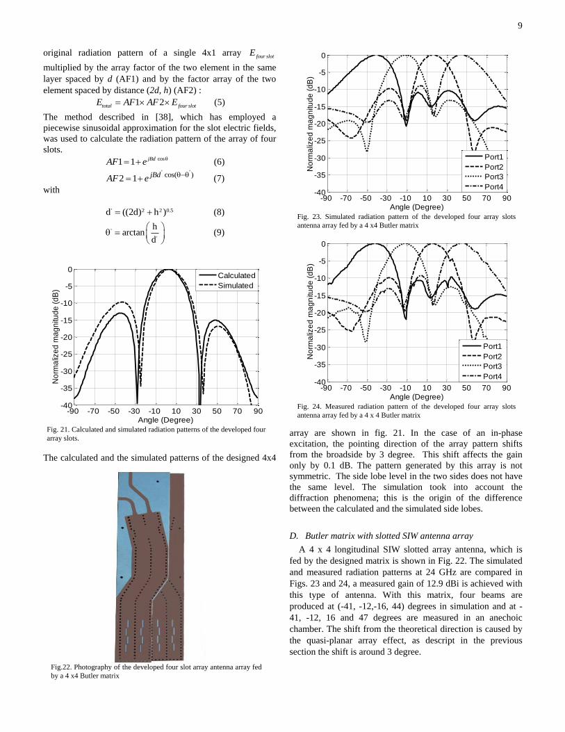
9
original radiation pattern of a single 4x1 array four slotE
multiplied by the array factor of the two element in the same
layer spaced by d (AF1) and by the factor array of the two
element spaced by distance (2d, h) (AF2) :
1 2 total four slotE AF AF E (5)
The method described in [38], which has employed a
piecewise sinusoidal approximation for the slot electric fields,
was used to calculate the radiation pattern of the array of four
slots. cos1 1 jBdAF e (6)
' 'cos( )2 1 jBdAF e (7)
with
' 2 2 0.5d ((2d) h ) (8)
'
'
harctan
d
(9)
The calculated and the simulated patterns of the designed 4x4
array are shown in fig. 21. In the case of an in-phase
excitation, the pointing direction of the array pattern shifts
from the broadside by 3 degree. This shift affects the gain
only by 0.1 dB. The pattern generated by this array is not
symmetric. The side lobe level in the two sides does not have
the same level. The simulation took into account the
diffraction phenomena; this is the origin of the difference
between the calculated and the simulated side lobes.
D. Butler matrix with slotted SIW antenna array
A 4 x 4 longitudinal SIW slotted array antenna, which is
fed by the designed matrix is shown in Fig. 22. The simulated
and measured radiation patterns at 24 GHz are compared in
Figs. 23 and 24, a measured gain of 12.9 dBi is achieved with
this type of antenna. With this matrix, four beams are
produced at (-41, -12,-16, 44) degrees in simulation and at -
41, -12, 16 and 47 degrees are measured in an anechoic
chamber. The shift from the theoretical direction is caused by
the quasi-planar array effect, as descript in the previous
section the shift is around 3 degree.
-90 -70 -50 -30 -10 10 30 50 70 90-40
-35
-30
-25
-20
-15
-10
-5
0
Angle (Degree)
No
rma
lize
d m
ag
nitu
de
(d
B)
Port1
Port2
Port3
Port4
Fig. 23. Simulated radiation pattern of the developed four array slots
antenna array fed by a 4 x4 Butler matrix
-90 -70 -50 -30 -10 10 30 50 70 90-40
-35
-30
-25
-20
-15
-10
-5
0
Angle (Degree)
No
rma
lize
d m
ag
nitu
de
(d
B)
Port1
Port2
Port3
Port4
Fig. 24. Measured radiation pattern of the developed four array slots
antenna array fed by a 4 x 4 Butler matrix
Fig.22. Photography of the developed four slot array antenna array fed
by a 4 x4 Butler matrix
-90 -70 -50 -30 -10 10 30 50 70 90-40
-35
-30
-25
-20
-15
-10
-5
0
Angle (Degree)
No
rma
lize
d m
ag
nitu
de
(d
B)
Calculated
Simulated
Fig. 21. Calculated and simulated radiation patterns of the developed four
array slots.

10
V. CONCLUSIONS
A four-port SIW Butler matrix has been proposed, designed
and demonstrated using a double-layered dielectric structure.
The proposed configuration avoids the line crossing, which
makes the matrix more compact and low loss. A broadside
coupled 3-dB coupler and side wall 3-dB coupler with
incorporated phase shifts are developed using the SIW
technology. These components are then combined to build up
the Butler matrix. The simulation of the developed matrix
shows excellent performances in the bandwidth of 22-26GHz,
with ±1dB power equality, a 0.35 dB of loss in the central
frequency and the required phase shift between output ports.
To demonstrate the performance of the proposed matrix, the
designed matrix is used to feed a four short ALTSA antenna.
The simulated and measured results show good agreements
over a wide bandwidth which validates the proposed concept.
Subsequently, a 4 x 4 array antenna with longitudinal slots
etched on the broad wall of the SIW has been designed and
integrated with the proposed matrix, which are then fabricated
and measured. The proposed topology can easily be used to
design 8x8 Butler matrix and higher-order structures.
Acknowledgement
The authors wish to thank J. Gauthier and S. Dubé, Poly-
Grames Research Center, École Polytechnique de Montreal
for their outstanding technical support and fabrication process.
Financial support from the Natural Sciences and Engineering
Research Council of Canada (NSERC) is gratefully
acknowledged.
REFERENCES
[1] J.J. Hung, Ku- to W-Band SiGe RFIC and RF MEMS Sub-systems, PH.D
These, the University of Michigan, 2005.
[2] L.H. Eriksson and B.O. As, "A high performance automotive radar for
automatic AICC cars," IEEE Radar Conference, pp.380-385, Mai 1995.
[3] M.E. Russell, A. Crain, A. Curran, R.A. Campbell, C.A. Drubin and
W.F. Micciolt, ―Millimeter-wave radar sensor for automotive intelligent
cruise control (ICC),‖ IEEE Trans. on Microwave Theory and Technique,
vol. 45 no. 12 1997 pp.2444-2453
[4] K. Schuler, M. Younis, R. Lenz and W. Wiesbeck, ―Array Design for
Automotive Digital Beamforming Radar System," IEEE Radar
Conference, pp.435 – 440, May 2005.
[5] S. Mosca, F. Bilotti, A. Toscano, and L. Vegni, ―A novel design method
for Blass matrix beam-forming networks,‖ IEEE Trans. Antennas
Propag., vol. 50, no. 2, pp. 225–232, Feb. 2002.
[6] N.J.G. Fonseca, ―Study and Design of a S-band 4x4 Nolen Matrix for
Satellite Digital Multimedia Broadcasting Applications,‖ 12th
International Symp. ANTEM URSI. Montreal (QC), pp. 481-484, July 16-
19 2006.
[7] J. Butler and R. Lowe, ―Beam forming matrix simplifies design of
electronically scanned antennas,‖ Applied Superconductivity, IEEE
Transactions on, vol. 9, pp. 170–173, Apr 1961.
[8] H. Mosallaei and Y. Rahmat-Samii, ―Nonuniform Luneburg and two-shell
lens antennas: radiation characteristics and design optimization,‖ IEEE
Transactions Antennas and Propagation, Vol 49, Iss 1, pp.60 - 69, Jan
2001.
[9] A. Angelucci, P. Audagnotto, P. Corda, F. Piarulli, and B. Piovano,
―Evolution of microstrip components for mobile communication
systems,‖ 1994 Third Annual International Conference on Universal
Personal Communications. pp.16 – 20. Oct. 1994.
[10] M. Nedil, T.A. Denidni ―Novel Butler Matrix Using CPW Multilayer
Technology,‖ IEEE Transactions on Microwave Theory and Techniques,
vol. 54, pp. 499 - 507. 1, January 2006.
[11] R. Levi, ―High power X-band Butler matrix,‖ Microw. J., Apr. 1984.
[12] D. Madrid, B. Vidal, A. Martinez, V. Polo, J.L. Corral and J. Marti, "A
novel 2N beams heterodyne optical beamforming architecture based on
NxN optical Butler matrices," MTT-S International Microwave
Symposium Digest, 2002 IEEE, Vol. 3, 2002, pp. 1945-1948.
[13] S. Yamamoto, J. Hirokawa, and M. Ando , ―A Single-Layer Hollow-
Waveguide 8-Way Butler Matrix,‖ IEICE Trans. Electron.,
vol.89, no7, pp. 1080-1088 2006
[14] S. Yamamoto, J. Hirokawa, and M. Ando, "A beam switching slot array
with a 4-way Butler matrix installed in single layer post-wall
waveguides," IEICE Trans. Commun., vol.E86-B, no.5, pp.1653–1659,
May 2003.
[15] H. J. MOODY, "The Systematic design of the Butler matrix," IEEE
Trans., 1964, pp. 786-788
[16] S.F. Peik, B. Jolley and R.R. Mansour, "High temperature
superconductive Butler matrix beam former for satellite applications",
Microwave Symposium Digest,1999 IEEE MTT-S International, Vol. 4,
1999, pp. 1543-1546
[17] M. Bona, L. Manholm, J. P. Starskiand B. Svensson, " Low-Loss
Compact Butler Matrix for a Microstrip Antenna,‖ IEEE Transactions on
Microwave Theory and Techniques , vol. 5450, pp. 2069–20752002,
[18] J. Hirokawa, M. Furukawa, K. Tsunekawa and N. Goto, ―Double-
Layer Structure of Rectangular-Waveguides for Butler Matrix,‖ European
Microwave Conference, 2002. 32nd , Oct. 2002 pp:1-4.
[19] Y. Cassivi, D. Deslandes and K. Wu, ―Substrate integrated waveguide
directional couplers,‖ ASIA-Pacific Conf. 2002, Kyoto,Nov. 2002.
[20] Z.C. Hao, W. Hong, J.X. Chen, H.X. Zhou and K. Wu ―Single-layer
substrate integrated waveguide directional couplers,‖ IEE Proc.-Microw.
Antennas Propag., Vol. 153, No. 5, October 2006.
[21] B. Liu, W. Hong and Z. C. Hao, et al., "Substrate integrated waveguide
180-degree narrow-wall directional coupler," Microwave Conference
Proceedings, 2005. APMC 2005,.
[22] N. Marcuvitz, Waveguide Handbook, MIT Radiation Laboratory Series,
Vol. 10,McGraw-Hill Book Company, 1951.
[23] W. Che, L. Xu, S. Dong, P. Russer, ―Theoretical analysis and numerical
verification of waveguide-type directional coupler constructed into thin
double-layer dielectric substrate,‖ Microwave and optical technology
letters, v : 50 no : 5 pg : 1397,2008.
[24] E. Hadge, ― Compact Top-Wall Hybrid Junction,‖Transactions of the IRE
Professional Group on Microwave Theory and Techniques,
Vol1, Iss1, pp:29 - 30 March 1953.
[25] H. A. Bethe, ―Theory of Diffraction by Small Holes,‖ Phys. Rev. Vol66,
pp.163-182, Oct. 1944.
[26] J. Uher, J. Bornemann, U. Rosenberg, Waveguide components for
antenna feed systems: Theory and CAD, Artech House Publishers,1993.
[27] R. Levy, ―Analysis and synthesis of waveguide multi-aperture directional
couplers,‖ MTT IEEE Trans-16, pp. 995-1006. ., 1968,
[28] D. Deslandes and K. Wu, ―Integrated microstrip and rectangular
waveguide in planar form,‖ IEEE MicrowaveWireless Compon. Lett., vol.
11, pp. 68–70, Feb. 2001.
[29] A. Angelucci, P. Audagnotto, P.Corda, P.Obino, F. Piarulli, B. Piovano,
―high performance microstrip networks for multibeam and reconfigurable
operation in mobile-radio systems,‖ Global Telecommunications
Conference, 1994. Volume 3, 28 Nov.-2 Dec. 1994 pp: 1717 - 1721 vol.3.
[30] Z.C. Hao, W. Hong, J. Chen, and K. Wu, ―A novel feeding technique for
antipodal linearly tapered slot antenna array, ‖ IEEE MTT-S Int.
Microwave Symp. Dig., pp. 1641-1643, Long Beach, USA, June 2005.
[31] K.S. Yngvesson, T.L. Korzeniowski, Y.-S. Kim, E.L. Kollberg, and J.F.
Johansson ―The tapered slot antenna – A new integrated element for
millimeter-wave Aapplications,‖ IEEE Trans. Microwave Theory Tech.,
vol.37, pp. 365-374, Feb. 1989.
[32] I. Wood, D. Dousset, J. Bornemann, and S. Claude, ―Linear tapered slot
antenna with substrate integrated waveguide feed Antennas,‖
Propagation International Symposium, 9-15 June 2007 pp:4761 – 4764.
[33] S. Gruszczyn´ski, K. Wincza, and K. Sachse, ― Reduced Sidelobe Four-
Beam N-Element A ntennaArrays Fed by 4 N Butler Matrices,‖ IEEE
Antennas AND Wireless Propagation Letters, VOL. 5, 2006
[34] A. Fragola, M. Orefice, and M. Pirola, ―A modified Butler matrix for
tapered excitation of scanned arrays,‖ in Proc. Antennas and
PropagationSociety Int. Symp., vol. 4, Jul. 2001, pp. 784–787.

11
[35] E. C. DuFort, ―Optimum low sidelobe high crossover multiple beam
antennas,‖ IEEE Trans. Antennas Propag., vol. AP-33, no. 9, pp. 946–
954, Sep. 1985.
[36] W. R. Li, C.Y. Chu, K. H. Lin, and S. F. Chang, ―Switched-beam antenna
based on modified Butler matrix with lowsidelobe level,‖ Electron.
Lett.,vol. 40, no. 5, pp. 290–292, Mar. 2004
[37] L. Yan, W. Hong, G. Hua, J. Chen, K. Wu, and T. J. Cui, "Simulation and
experiment on SIW slot array antennas," IEEE Microwave and Wireless
Component Letters, vol. 14, pp. 446-448, Sept. 2004.
[38] J. C. Coetzee, ―Off-center-frequency analysis of a complete planar
slotted-waveguide array consisting of subarrays,‖ IEEE Trans. Antennas
Propagat., vol. 48, pp. 1746–1755, Nov. 2000.

74
ARTICLE III: DESIGN AND IMPLEMENTATION OF A PLANAR 4×4
BUTLER MATRIX IN SIW TECHNOLOGY FOR WIDE BAND HIGH
POWER APPLICATIONS
Tarek Djerafi, Nelson J.G. Fonseca, et Ke Wu
Soumis le 14 octobre 2010 à IEEE Transactions on Microwave Theory and Techniques.
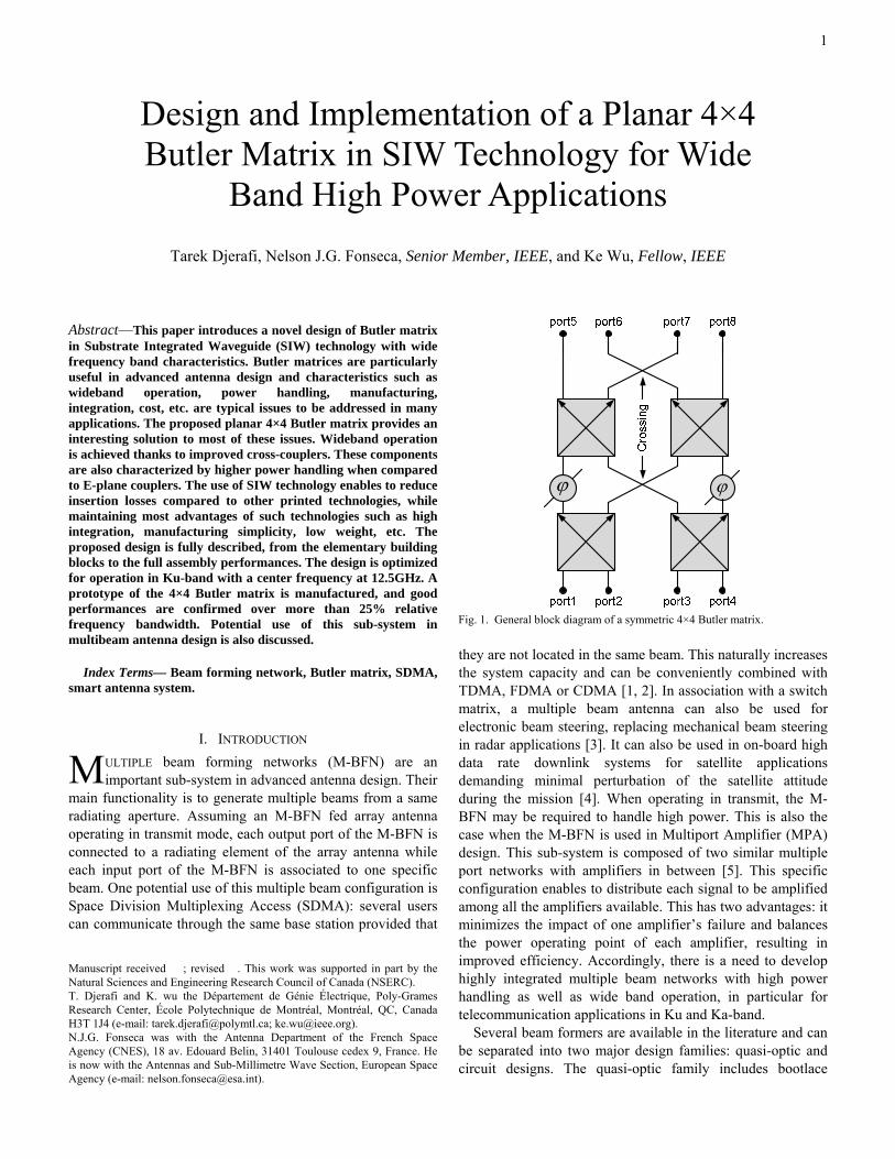
1
Abstract—This paper introduces a novel design of Butler matrix in Substrate Integrated Waveguide (SIW) technology with wide frequency band characteristics. Butler matrices are particularly useful in advanced antenna design and characteristics such as wideband operation, power handling, manufacturing, integration, cost, etc. are typical issues to be addressed in many applications. The proposed planar 4×4 Butler matrix provides an interesting solution to most of these issues. Wideband operation is achieved thanks to improved cross-couplers. These components are also characterized by higher power handling when compared to E-plane couplers. The use of SIW technology enables to reduce insertion losses compared to other printed technologies, while maintaining most advantages of such technologies such as high integration, manufacturing simplicity, low weight, etc. The proposed design is fully described, from the elementary building blocks to the full assembly performances. The design is optimized for operation in Ku-band with a center frequency at 12.5GHz. A prototype of the 4×4 Butler matrix is manufactured, and good performances are confirmed over more than 25% relative frequency bandwidth. Potential use of this sub-system in multibeam antenna design is also discussed.
Index Terms— Beam forming network, Butler matrix, SDMA, smart antenna system.
I. INTRODUCTION
ULTIPLE beam forming networks (M-BFN) are an important sub-system in advanced antenna design. Their
main functionality is to generate multiple beams from a same radiating aperture. Assuming an M-BFN fed array antenna operating in transmit mode, each output port of the M-BFN is connected to a radiating element of the array antenna while each input port of the M-BFN is associated to one specific beam. One potential use of this multiple beam configuration is Space Division Multiplexing Access (SDMA): several users can communicate through the same base station provided that
Manuscript received ; revised . This work was supported in part by the Natural Sciences and Engineering Research Council of Canada (NSERC). T. Djerafi and K. wu the Département de Génie Électrique, Poly-Grames Research Center, École Polytechnique de Montréal, Montréal, QC, Canada H3T 1J4 (e-mail: [email protected]; [email protected]). N.J.G. Fonseca was with the Antenna Department of the French Space Agency (CNES), 18 av. Edouard Belin, 31401 Toulouse cedex 9, France. He is now with the Antennas and Sub-Millimetre Wave Section, European Space Agency (e-mail: [email protected]).
they are not located in the same beam. This naturally increases the system capacity and can be conveniently combined with TDMA, FDMA or CDMA [1, 2]. In association with a switch matrix, a multiple beam antenna can also be used for electronic beam steering, replacing mechanical beam steering in radar applications [3]. It can also be used in on-board high data rate downlink systems for satellite applications demanding minimal perturbation of the satellite attitude during the mission [4]. When operating in transmit, the M-BFN may be required to handle high power. This is also the case when the M-BFN is used in Multiport Amplifier (MPA) design. This sub-system is composed of two similar multiple port networks with amplifiers in between [5]. This specific configuration enables to distribute each signal to be amplified among all the amplifiers available. This has two advantages: it minimizes the impact of one amplifier’s failure and balances the power operating point of each amplifier, resulting in improved efficiency. Accordingly, there is a need to develop highly integrated multiple beam networks with high power handling as well as wide band operation, in particular for telecommunication applications in Ku and Ka-band.
Several beam formers are available in the literature and can be separated into two major design families: quasi-optic and circuit designs. The quasi-optic family includes bootlace
Design and Implementation of a Planar 4×4 Butler Matrix in SIW Technology for Wide
Band High Power Applications
Tarek Djerafi, Nelson J.G. Fonseca, Senior Member, IEEE, and Ke Wu, Fellow, IEEE
M
Fig. 1. General block diagram of a symmetric 4×4 Butler matrix.
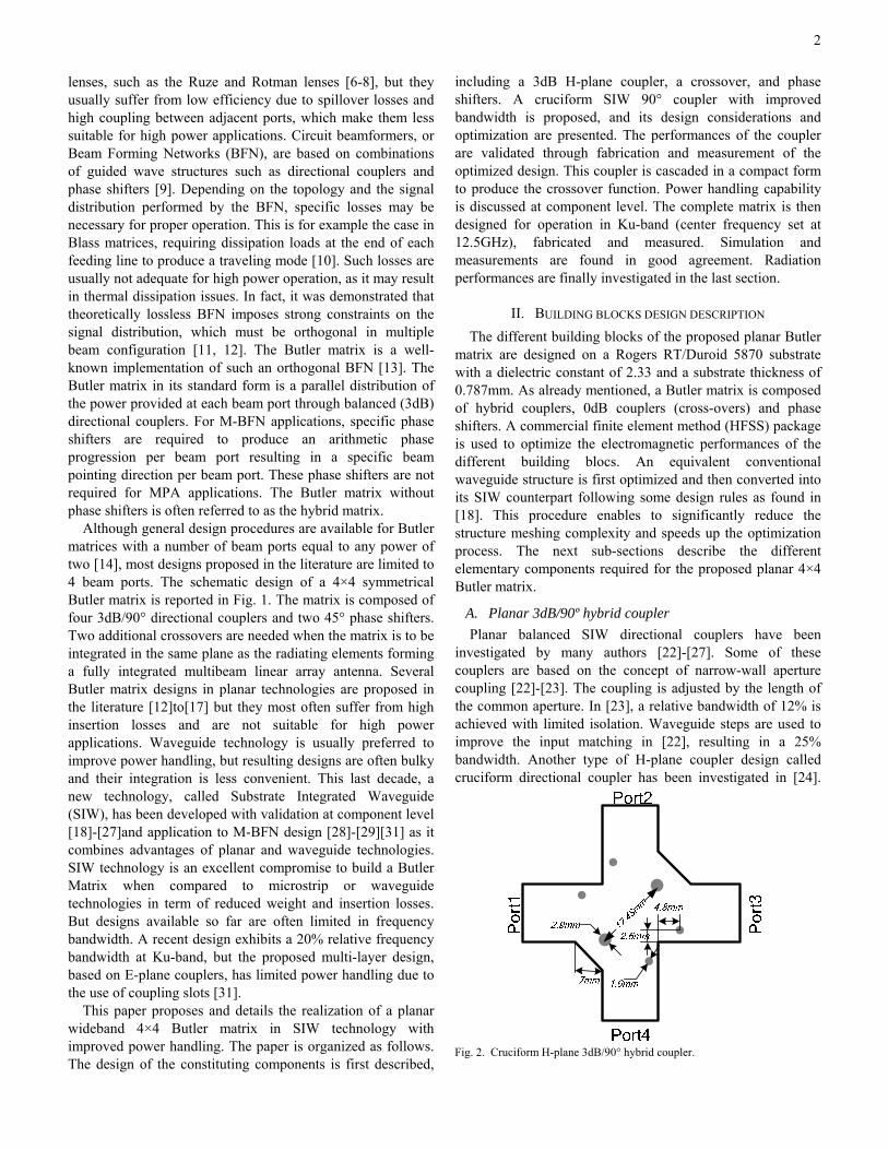
2
lenses, such as the Ruze and Rotman lenses [6-8], but they usually suffer from low efficiency due to spillover losses and high coupling between adjacent ports, which make them less suitable for high power applications. Circuit beamformers, or Beam Forming Networks (BFN), are based on combinations of guided wave structures such as directional couplers and phase shifters [9]. Depending on the topology and the signal distribution performed by the BFN, specific losses may be necessary for proper operation. This is for example the case in Blass matrices, requiring dissipation loads at the end of each feeding line to produce a traveling mode [10]. Such losses are usually not adequate for high power operation, as it may result in thermal dissipation issues. In fact, it was demonstrated that theoretically lossless BFN imposes strong constraints on the signal distribution, which must be orthogonal in multiple beam configuration [11, 12]. The Butler matrix is a well-known implementation of such an orthogonal BFN [13]. The Butler matrix in its standard form is a parallel distribution of the power provided at each beam port through balanced (3dB) directional couplers. For M-BFN applications, specific phase shifters are required to produce an arithmetic phase progression per beam port resulting in a specific beam pointing direction per beam port. These phase shifters are not required for MPA applications. The Butler matrix without phase shifters is often referred to as the hybrid matrix.
Although general design procedures are available for Butler matrices with a number of beam ports equal to any power of two [14], most designs proposed in the literature are limited to 4 beam ports. The schematic design of a 4×4 symmetrical Butler matrix is reported in Fig. 1. The matrix is composed of four 3dB/90° directional couplers and two 45° phase shifters. Two additional crossovers are needed when the matrix is to be integrated in the same plane as the radiating elements forming a fully integrated multibeam linear array antenna. Several Butler matrix designs in planar technologies are proposed in the literature [12]to[17] but they most often suffer from high insertion losses and are not suitable for high power applications. Waveguide technology is usually preferred to improve power handling, but resulting designs are often bulky and their integration is less convenient. This last decade, a new technology, called Substrate Integrated Waveguide (SIW), has been developed with validation at component level [18]-[27]and application to M-BFN design [28]-[29][31] as it combines advantages of planar and waveguide technologies. SIW technology is an excellent compromise to build a Butler Matrix when compared to microstrip or waveguide technologies in term of reduced weight and insertion losses. But designs available so far are often limited in frequency bandwidth. A recent design exhibits a 20% relative frequency bandwidth at Ku-band, but the proposed multi-layer design, based on E-plane couplers, has limited power handling due to the use of coupling slots [31].
This paper proposes and details the realization of a planar wideband 4×4 Butler matrix in SIW technology with improved power handling. The paper is organized as follows. The design of the constituting components is first described,
including a 3dB H-plane coupler, a crossover, and phase shifters. A cruciform SIW 90° coupler with improved bandwidth is proposed, and its design considerations and optimization are presented. The performances of the coupler are validated through fabrication and measurement of the optimized design. This coupler is cascaded in a compact form to produce the crossover function. Power handling capability is discussed at component level. The complete matrix is then designed for operation in Ku-band (center frequency set at 12.5GHz), fabricated and measured. Simulation and measurements are found in good agreement. Radiation performances are finally investigated in the last section.
II. BUILDING BLOCKS DESIGN DESCRIPTION
The different building blocks of the proposed planar Butler matrix are designed on a Rogers RT/Duroid 5870 substrate with a dielectric constant of 2.33 and a substrate thickness of 0.787mm. As already mentioned, a Butler matrix is composed of hybrid couplers, 0dB couplers (cross-overs) and phase shifters. A commercial finite element method (HFSS) package is used to optimize the electromagnetic performances of the different building blocs. An equivalent conventional waveguide structure is first optimized and then converted into its SIW counterpart following some design rules as found in [18]. This procedure enables to significantly reduce the structure meshing complexity and speeds up the optimization process. The next sub-sections describe the different elementary components required for the proposed planar 4×4 Butler matrix.
A. Planar 3dB/90º hybrid coupler
Planar balanced SIW directional couplers have been investigated by many authors [22]-[27]. Some of these couplers are based on the concept of narrow-wall aperture coupling [22]-[23]. The coupling is adjusted by the length of the common aperture. In [23], a relative bandwidth of 12% is achieved with limited isolation. Waveguide steps are used to improve the input matching in [22], resulting in a 25% bandwidth. Another type of H-plane coupler design called cruciform directional coupler has been investigated in [24].
Fig. 2. Cruciform H-plane 3dB/90° hybrid coupler.
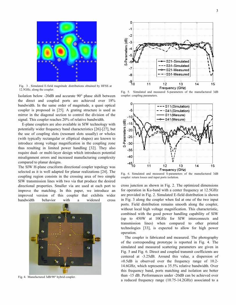
3
Isolation below -20dB and accurate 90° phase shift between the direct and coupled ports are achieved over 18% bandwidth. In the same order of magnitude, a quasi optical coupler is proposed in [25]. A grating structure is used as mirror in the diagonal section to control the division of the signal. This coupler reaches 20% of relative bandwidth.
E-plane couplers are also available in SIW technology with potentially wider frequency band characteristics [26]-[27], but the use of coupling slots (resonant slots usually) or wholes (with typically rectangular or elliptical shapes) are known to introduce strong voltage magnification in the coupling zone thus resulting in limited power handling [32]. They also require dual- or multi-layer design which introduces potential misalignment errors and increased manufacturing complexity compared to planar designs. The SIW H-plane cruciform directional coupler topology was selected as it is well adapted for planar realizations [24]. The coupling region consists in the crossing area of two simple SIW transmission lines with two via that produce the desired directional properties. Smaller via are used at each port to improve the matching. In this paper, we introduce an improved version of this coupler that exhibits wider bandwidth behavior with a widened cross
cross junction as shown in Fig. 2. The optimized dimensions for operation in Ku-band with a center frequency at 12.5GHz are provided in Fig. 2. Simulated E-field distribution is shown in Fig. 3 along the coupler when fed at one of the two input ports. Field distribution remains smooth along the coupler, without local high voltage magnification. This characteristic, combined with the good power handling capability of SIW (up to 450W at 10GHz for SIW interconnects and transmission lines) when compared to other printed technologies [33], is expected to allow for high power operation. The coupler is fabricated and measured. The photography of the corresponding prototype is reported in Fig. 4. The simulated and measured scattering parameters are given in Fig. 5 and Fig. 6. Direct and coupled transmit coefficients are centered at -3.25dB. Around this value, a dispersion of ±0.5dB is observed over the frequency range of 10.2-14.6GHz, which represents a 35.5% relative bandwidth. Over this frequency band, ports matching and isolation are better than -15 dB. Performances under -20dB can be achieved over a reduced frequency range (10.75-14.2GHz) associated to a
Fig. 4. Manufactured 3dB/90° hybrid coupler.
Fig. 6. Simulated and measured S-parameters of the manufactured 3dBcoupler: return losses and input ports isolation.
Fig. 5. Simulated and measured S-parameters of the manufactured 3dBcoupler: coupling parameters.
Fig. 3 . Simulated E-field magnitude distributions obtained by HFSS at 12.5GHz, along the coupler.
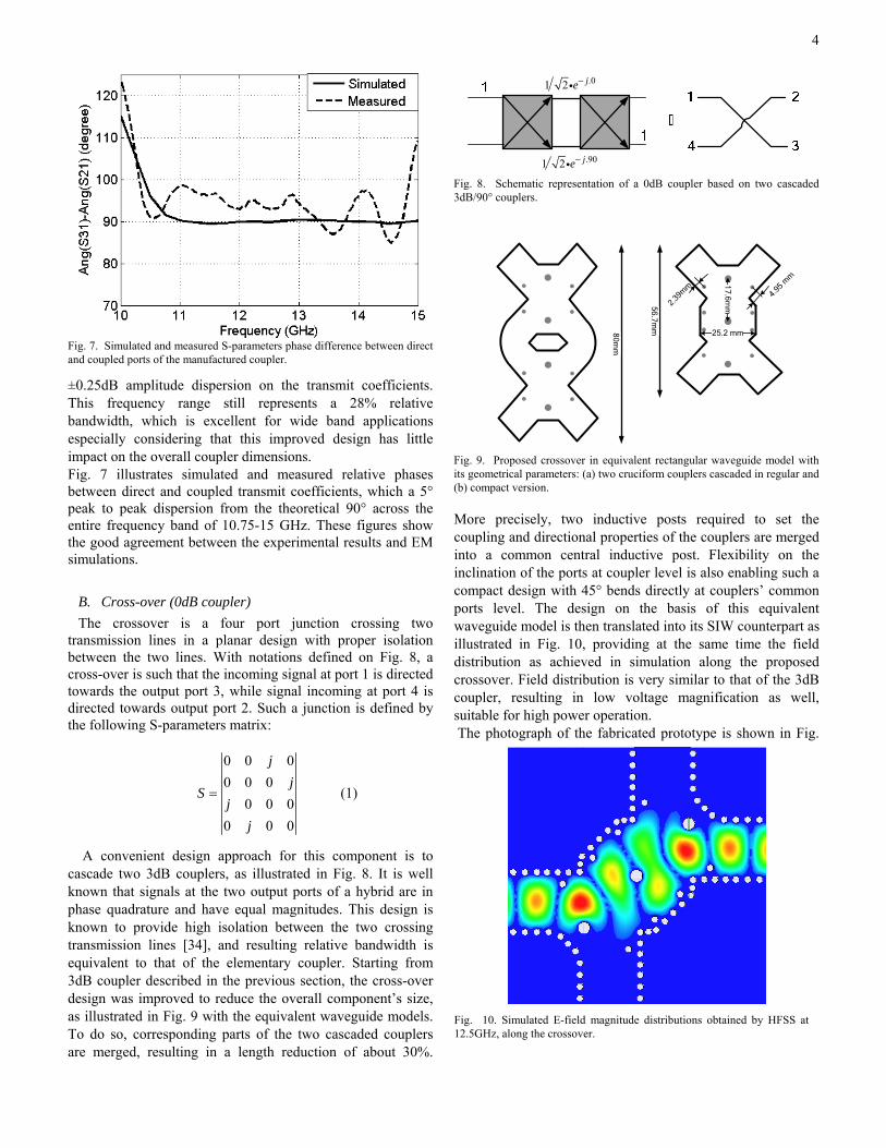
4
±0.25dB amplitude dispersion on the transmit coefficients. This frequency range still represents a 28% relative bandwidth, which is excellent for wide band applications especially considering that this improved design has little impact on the overall coupler dimensions. Fig. 7 illustrates simulated and measured relative phases between direct and coupled transmit coefficients, which a 5° peak to peak dispersion from the theoretical 90° across the entire frequency band of 10.75-15 GHz. These figures show the good agreement between the experimental results and EM simulations.
B. Cross-over (0dB coupler)
The crossover is a four port junction crossing two transmission lines in a planar design with proper isolation between the two lines. With notations defined on Fig. 8, a cross-over is such that the incoming signal at port 1 is directed towards the output port 3, while signal incoming at port 4 is directed towards output port 2. Such a junction is defined by the following S-parameters matrix:
0 0 0
0 0 0
0 0 0
0 0 0
j
jS
j
j
(1)
A convenient design approach for this component is to cascade two 3dB couplers, as illustrated in Fig. 8. It is well known that signals at the two output ports of a hybrid are in phase quadrature and have equal magnitudes. This design is known to provide high isolation between the two crossing transmission lines [34], and resulting relative bandwidth is equivalent to that of the elementary coupler. Starting from 3dB coupler described in the previous section, the cross-over design was improved to reduce the overall component’s size, as illustrated in Fig. 9 with the equivalent waveguide models. To do so, corresponding parts of the two cascaded couplers are merged, resulting in a length reduction of about 30%.
More precisely, two inductive posts required to set the coupling and directional properties of the couplers are merged into a common central inductive post. Flexibility on the inclination of the ports at coupler level is also enabling such a compact design with 45° bends directly at couplers’ common ports level. The design on the basis of this equivalent waveguide model is then translated into its SIW counterpart as illustrated in Fig. 10, providing at the same time the field distribution as achieved in simulation along the proposed crossover. Field distribution is very similar to that of the 3dB coupler, resulting in low voltage magnification as well, suitable for high power operation. The photograph of the fabricated prototype is shown in Fig.
Fig. 7. Simulated and measured S-parameters phase difference between directand coupled ports of the manufactured coupler.
Fig. 10. Simulated E-field magnitude distributions obtained by HFSS at 12.5GHz, along the crossover.
.901 2 je
.01 2 je
Fig. 8. Schematic representation of a 0dB coupler based on two cascaded 3dB/90° couplers.
56.7mm80m
m
17.6mm
25.2 mm
4.95
mm
2.39
mm
Fig. 9. Proposed crossover in equivalent rectangular waveguide model withits geometrical parameters: (a) two cruciform couplers cascaded in regular and(b) compact version.
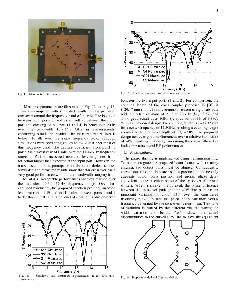
5
11. Measured parameters are illustrated in Fig. 12 and Fig. 13. They are compared with simulated results for the proposed crossover around the frequency band of interest. The isolation between input ports (1 and 2) as well as between the input port and crossing output port (1 and 4) is better than 20dB over the bandwidth 10.7-14.2 GHz in measurements, confirming simulation results. The measured return loss is below -10 dB over the same frequency band, although simulations were predicting values below -20dB ober most of this frequency band. The transmit coefficient from port1 to port3 has a worst case of 0.6dB over the 11-14GHz frequency range. Part of measured insertion loss originates from reflection higher than expected at the input port. However, the transmission loss is principally attributed to dielectric loss. Simulated and measured results show that this crossover has a very good performance with a broad bandwidth, ranging from 11 to 14GHz. Acceptable performances are even reached over the extended 10.5-14.6GHz frequency range. Over this extended bandwidth, the proposed junction provides insertion loss better than 1dB and the isolation between ports 1 and 4 better than 20 dB. The same level of isolation is also observed
between the two input ports (1 and 2). For comparison, the coupling length of the cross coupler proposed in [28] is l=20.17 mm (limited to the common section) using a substrate with dielectric constant of 2.17 at 26GHz (l/λr =2.57) and show good result over 1GHz (relative bandwidth of 3.8%). With the proposed design, the coupling length is l =32.32 mm for a center frequency of 12.5GHz, resulting a coupling length normalized to the wavelength of l/λr =2.05. The proposed design achieves good performances over a relative bandwidth of 24%, resulting in a design improving the state-of-the-art in both compactness and RF performances.
C. Phase shifters
The phase shifting is implemented using transmission line. To better integrate the proposed beam former with an array antenna, the output ports must be aligned. Consequently, curved transmission lines are used to produce simultaneously adequate output ports position and proper phase delay equivalent to the insertion phase of the crossover (0° phase shifter). When a simple line is used, the phase difference between the crossover path and the SIW line path has an important variation of about ±30° over the considered frequency range. In fact the phase delay variation versus frequency generated by the crossover is non-linear. This type of variation is caused by the different via, the waveguide width variation and bends. Fig.14 shows the added discontinuities to the curved SIW line to have the equivalent
Fig. 14. Proposed wide band 0° phase shifter.
Fig. 11. Manufactured 0dB coupler.
Fig. 12. Simulated and measured S-parameters: isolations.
Fig. 13. Simulated and measured S-parameters: return loss andtransmission.
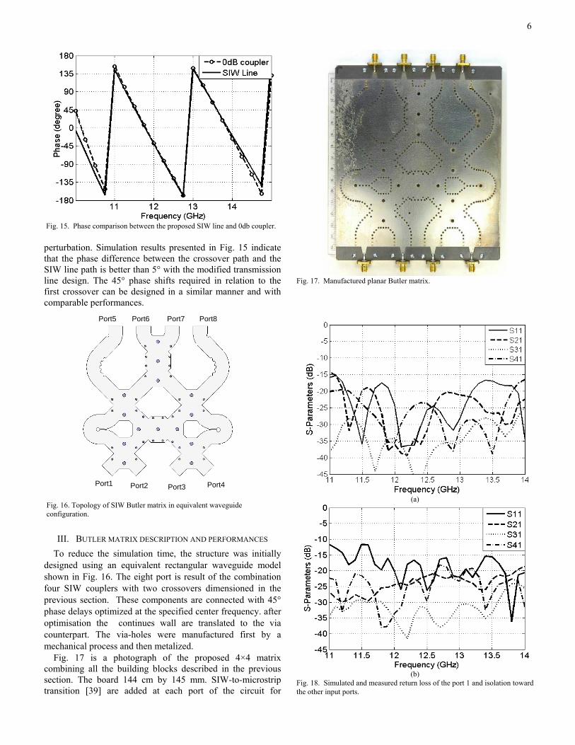
6
perturbation. Simulation results presented in Fig. 15 indicate that the phase difference between the crossover path and the SIW line path is better than 5° with the modified transmission line design. The 45° phase shifts required in relation to the first crossover can be designed in a similar manner and with comparable performances.
III. BUTLER MATRIX DESCRIPTION AND PERFORMANCES
To reduce the simulation time, the structure was initially designed using an equivalent rectangular waveguide model shown in Fig. 16. The eight port is result of the combination four SIW couplers with two crossovers dimensioned in the previous section. These components are connected with 45° phase delays optimized at the specified center frequency. after optimisation the continues wall are translated to the via counterpart. The via-holes were manufactured first by a mechanical process and then metalized.
Fig. 17 is a photograph of the proposed 4×4 matrix combining all the building blocks described in the previous section. The board 144 cm by 145 mm. SIW-to-microstrip transition [39] are added at each port of the circuit for
Port1 Port2 Port3 Port4
Port5 Port6 Port7 Port8
Fig. 16. Topology of SIW Butler matrix in equivalent waveguide configuration.
Fig. 15. Phase comparison between the proposed SIW line and 0db coupler.
Fig. 17. Manufactured planar Butler matrix.
(a)
(b) Fig. 18. Simulated and measured return loss of the port 1 and isolation toward the other input ports.
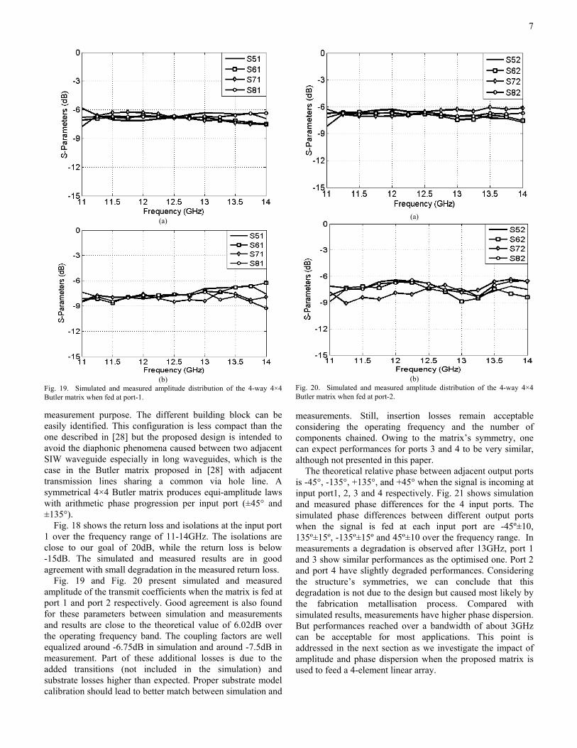
7
measurement purpose. The different building block can be easily identified. This configuration is less compact than the one described in [28] but the proposed design is intended to avoid the diaphonic phenomena caused between two adjacent SIW waveguide especially in long waveguides, which is the case in the Butler matrix proposed in [28] with adjacent transmission lines sharing a common via hole line. A symmetrical 4×4 Butler matrix produces equi-amplitude laws with arithmetic phase progression per input port (±45° and ±135°).
Fig. 18 shows the return loss and isolations at the input port 1 over the frequency range of 11-14GHz. The isolations are close to our goal of 20dB, while the return loss is below -15dB. The simulated and measured results are in good agreement with small degradation in the measured return loss.
Fig. 19 and Fig. 20 present simulated and measured amplitude of the transmit coefficients when the matrix is fed at port 1 and port 2 respectively. Good agreement is also found for these parameters between simulation and measurements and results are close to the theoretical value of 6.02dB over the operating frequency band. The coupling factors are well equalized around -6.75dB in simulation and around -7.5dB in measurement. Part of these additional losses is due to the added transitions (not included in the simulation) and substrate losses higher than expected. Proper substrate model calibration should lead to better match between simulation and
measurements. Still, insertion losses remain acceptable considering the operating frequency and the number of components chained. Owing to the matrix’s symmetry, one can expect performances for ports 3 and 4 to be very similar, although not presented in this paper.
The theoretical relative phase between adjacent output ports is -45°, -135°, +135°, and +45° when the signal is incoming at input port1, 2, 3 and 4 respectively. Fig. 21 shows simulation and measured phase differences for the 4 input ports. The simulated phase differences between different output ports when the signal is fed at each input port are -45º±10, 135º±15º, -135º±15º and 45º±10 over the frequency range. In measurements a degradation is observed after 13GHz, port 1 and 3 show similar performances as the optimised one. Port 2 and port 4 have slightly degraded performances. Considering the structure’s symmetries, we can conclude that this degradation is not due to the design but caused most likely by the fabrication metallisation process. Compared with simulated results, measurements have higher phase dispersion. But performances reached over a bandwidth of about 3GHz can be acceptable for most applications. This point is addressed in the next section as we investigate the impact of amplitude and phase dispersion when the proposed matrix is used to feed a 4-element linear array.
(a)
(b)
Fig. 19. Simulated and measured amplitude distribution of the 4-way 4×4 Butler matrix when fed at port-1.
(a)
(b) Fig. 20. Simulated and measured amplitude distribution of the 4-way 4×4 Butler matrix when fed at port-2.
8
IV. RADIATION PATTERNS
We use the measured amplitudes and phases of the proposed Butler matrix to evaluate the beam-patterns radiated by a linear array antenna defined analytically. The field pattern of the elementary radiator is modelled by the following formula:
1.3( ) cos( ) E
This approximates the radiation pattern of a standard square-patch microstrip antenna, which is a simple and common elementary radiator design in printed planar array antennas. Neglecting coupling effects and using linear array factor formulation, we compute the radiation patterns when the 4-element linear array with 0.6 λ of spacing is fed by the proposed matrix. The results are reported in Fig. 21. Each arithmetic phase progression produces a different beam pointing. Pointing directions achieved with measured data are respectively -12, 30.8, -31 and 12°. Theoretical values are -10, 30,-30 and 10°, resulting in a worst case pointing error of 2°. To study the variation of beam direction with the frequency, the same considerations are taken into account over the band 11-14GHz, the results a. For port1 can be observed that the
angler shown in Fig. 22e hover around 10 degrees by 1 degree, as expected. For port 2 this variation increases and varies between 31 and 38 degrees. The variation of the beam squint increase with direction angle. This variation is very small and very little influence the gain in the main direction of pointing. The measurement results are very close to simulations.
V. CONCLUSION
A 4×4 Butler matrix has been designed in Ku band with a central frequency of 12.5GHz. Based on SIW technology, the proposed system has the advantages of low cost, light weight and ease of fabrication. The elementary building blocks are designed for wideband operation and associated to evaluate the overall matrix performances. A 3 dB coupler as 0 dB coupler based on the substrate integrated waveguide (SIW) technology are proposed and designed around 12.5GHz and fabricated using a standard PCB process. The measured results show a good agreement with the designed and simulated results. Obtained over 23% of bandwidth and less
Fig. 22. Variation of beam direction with the frequency
(a)
(b) Fig. 20. Simulated and measured output phase distribution per input port.
Fig. 21. Simulated radiation patterns based on measured beam forming matrixperformances.

9
0.6dB in 8.3 % of target bandwidth. The proposed crossover SIW junction is found to be very useful for the development of high-performance and compact-sized Butler matrix. Because of the phase shift slope of crossover is bigger than that of normal transmission line, via holes are placed inside the waveguide to reduce this effect.
Simulated and measured results are in good agreement and demonstrate a possible operating bandwidth of about 3GHz. The proposed Butler matrix could advantageously be used To reduce interference problem in wireless communications systems, this matrix can he used as a beam forming for multibeam antenna arrays
REFERENCES [1] A. EL. Zooghby, “Potentials of Smart Antennas In CDMA Systems and
Uplink Inprovements” , IEEE Antennas and Propagation Magazine , October 2001 , Vol. 43, No. 5
[2] L. C. Godara "Application of antenna arrays to mobile communications, Part II: Beam-forming and direction-of-arrival considerations", Proc. IEEE, vol. 85, pp. 1195 1997.
[3] F.,Jr. Cladwell,; J.S. Kenney and I.A. Ingram, “Design and Implementation of a Switched-Beam Smart Antenna for an 802.11b Wireless Access Point,” Radio and Wireless Conference, 2002. RAWCON 2002. pp. 55 - 58
[4] A.M. Polegre, G. Caille, L. Boyer, A. Roederer, “Semi-Active Conformal Array for ESA’s GAIA Mission,” IEEE AP-S Int. Symp. 2004, Vol. 4, 20-25 June 2004, pp. 4108-4111.
[5] S. Egami, M. Kawai, “An Adaptive Multiple Beam System Concept,” IEEE Journal on Selected Areas in Communications, Vol. SAC-5, No. 4 , pp. 630-636, Mai 1987.
[6] W. Rotman, R. Turner, “Wide-Angle Microwave Lens for Line Source Applications,” IEEE Trans. Antennas and Propag., Vol. 11, No. 6, pp. 623-632, Nov. 1963.
[7] J.P. Shelton, “Focusing Characteristics of Symmetrically Configured Bootlace Lenses,” IEEE Trans. Antennas and Propag., Vol. 26, pp. 513-518, Jul. 1978.
[8] J.S. Herd, D.M. Pozar, “Design of a Microstrip Antenna Array fed by a Rotman Lens,” IEEE AP-S Int. Symp., 1984, Vol. 22, Jun. 1984, pp. 729-732.
[9] P. S. Hall, S. J. Vetterlein, “Review of radio frequency beamforming techniques for scanned and multiple beam antennas", IEE Proceedings, vol. 137, Pt. H, No. 5, pp. 293-303, Oct. 1990.
[10] J. Blass, “Multidirectional Antenna, a New Approach to Stacked Beams,” IRE Int. Conf. Record, Vol. 8, Part 1, 1960, pp. 48-50.
[11] J.L. Allen, “A Theoretical Limitation on the Formation of Lossless Multiple Beams in Linear Arrays,” IEEE Trans. Antennas and Propag., Vol. 9, No. 7, pp. 350-352, Jul. 1961.
[12] W.D. White, “Pattern Limitations in Multiple-Beam Antennas,” IRE Trans. Antennas and Propag., Vol. 10, pp. 430-436, Jul. 1962.
[13] J. Butler and R. Lowe, “Beam forming matrix simplifies design of electronically scanned antennas,” Transactions on Applied Superconductivity, vol. 9, pp. 170–173, Apr 1961.
[14] H.J. Moody, “The Systematic Design of the Butler Matrix,” IEEE Trans. Antennas and Propag., Vol. 12, No. 6, Nov. 1964, pp. 786-788.
[15] J. He, B.-Z. Wang, Q.-Q. He, Y.-X. Xing, Andz.-L. Yin Wideband X-Band Microstrip Butler Matrix,”Progress In Electromagnetics Research, Pier 74, 131–140, 2007.
[16] L. Accatino, F. Muoio, B. Piovano, G. Caille, M. Mongiardo, “ Cad Of Waveguide Butler Matrices Including Mechanical And Thermal Constraints,” EuMC 2001
[17] M. Koubeissi, C. Decroze, T. Monediere, and B. Jecko, “A new methodto design a Butler matrix with broadside beam: Application to a multibeamantenna,” Microw. Opt. Technol. Lett., vol. 48, no. 1, pp. 35–40, Jan. 2006.
[18] K. Wu, D. Deslandes and Y. Cassivi, “The Substrate Integrated Circuits – A new concept for high-frequency electronics and optoelectronics,” TELSIKS’03, Nis, Yugoslavia, 2003, pp. P-III – P-X.
[19] Ismail, A., M. S. Razalli, M. A. Mahdi, R. S. A. R. Abdullah, N. K. Noordin, and M. F. A. Rasid, “X-band trisection substrate-integrated waveguide quasi-elliptic filter,” Progress In Electromagnetics Research, PIER 85, 133{145, 2008.
[20] W. Shen, X.W. Sun, W.-Y. Yin, J.-F. Mao, and Q.-F. Wei, “A novel single-cavity dual mode substrate integrated waveguide filter with non resonating node,” IEEE Microwave and Wireless Components Letters, Vol. 19, No. 6 ,pp.368-370, 2009.
[21] M. Henry, C. E. Free, B. S. Izqueirdo, J. Batchelor, and P.Young, “Millimeter wave substrate integrated waveguideantennas: design and fabrication analysis,” IEEE Trans.Advanced Packaging, vol. 32, no. 1, pp. 93-100, Feb. 2009.
[22] Y. Cassivi, D. Deslandes and K. Wu, “Substrate integrated waveguide directional couplers,” ASIA-Pacific Conf. 2002, Kyoto.
[23] Z.C. Hao, W. Hong, J.X. Chen, H.X. Zhou and K. Wu “Single-layer substrate integrated waveguide directional couplers,” IEE Proc.-Microw. Antennas Propag., Vol. 153, No. 5, October 2006.
[24] T. Djerafi and K. Wu, “Super-compact substrate integrated waveguide cruciform directional coupler,” IEEE Microw.Wireless Compon. Lett., vol. 17, no.11, pp. 757-759, Nov. 2007
[25] T. Djerafi, J. Gauthier, and K. Wu, “Quasi-optical cruciform substrate integrated waveguide (SIW) coupler for millimeter-wave systems,” International Microwave Symposium Digest (MTT), 2010 , pp 1-4.
[26] V.A. Labay, J. Bornemann, “E-plane directional couplers in substrate-integrated waveguide technology,” APMC, 2008.
[27] A. Ali, H. Aubert, N.J.G. Fonseca, F. Coccetti, “Wideband two-layer SIW coupler: design and experiment,” IET Electronics Letters, Vol. 45, No. 13, pp. 687-689, June 18, 2009.
[28] S. Yamamoto, J. Hirokawa and M. Ando, “A beam switching slot array with a 4-way Butler matrix installed in single layer post-wall waveguides,” IEICE Trans. on Communications, vol.E86-B, No.5, pp.1653-1659, May 2003.
[29] T. Djerafi, N.J.G. Fonseca, K. Wu, “Architecture and Implementation of Planar 4x4 Ku-Band Nolen Matrix Using SIW Technology”, APMC 2008, 16-20 Dec. 2008.
[30] E. Sbarra, L. Marcaccioli, R.V. Gatti, and R. Sorrentino, “A novel rotman lens in SIW technology,” Euro. Radar Conf. 2007, pp. 236-239, Oct.
[31] A. Ali, N. Fonseca, F. Coccetti and H. Aubert, “Novel two-layer broadband 4x4 Butler matrix in SIW technology for Ku band applications,” Asia Pacific Microw. Conf. (APMC’08), Dec. 08.
[32] European Cooperation for Space Standardization (ECSS), “Space Engineering – Multipaction design and test,” Ref. ECSS-E-20-01A, 5 May 2003.
[33] Y.J. Cheng, K. Wu, W. Hong, “Power Handling Capability of Substrate Integrated Waveguide Interconnects and Related Transmission Line Systems,” Trans. Advanced Packaging, Vol. 31, No. 4, pp. 900- 909, Nov. 2008.
[34] J. S. Wight, W. J. Chudobiak and V. Makios, “A Microstrip and Stripline Crossover Structure,” IEEE Transactions on Microwave Theory and Techniques, , pp. 270-270, May 1976.
[35] T. A. Denidni and T. E. Libar, “Wide Band Four-Port Butler Matrix for Switched Multibeam Antenna Arrays,” The 14th IEEE 2003 International Symposium on Personal, Indoor and Mobile Radio Communication Proceedings, pp.2461-2464.
[36] S. Yamamoto, J. Hirokawa and M. Ando, “Length reduction of a short-slot directional coupler in a single-layer dielectric substrate waveguide by removing dielectric near the side walls of the coupler,” IEEE AP-S International Symposium, June 2004, vol.3, pp.2353-2356.
[37] K. Wu, “Integration and interconnect techniques of planar and nonplanar structures for microwave and millimeter-wave circuits—Current status and future trend,” Asia-Pacific Microwave Conf. Proc., 2001, pp. 411–416. Invited paper.
[38] D. Deslandes and K. Wu, “Integrated microstrip and rectangular waveguide in planar form,” Microw. Guided Wave Lett., vol. 11, no. 2, pp. 68–70, Feb. 2001.
[39] D. Deslandes, and K. Wu, “Integrated microstrip and rectangular waveguide in planar form,” IEEE Microwave and Guided Wave Letters, vol. 11, no. 2, pp. 68-70, February 2001.

84
ARTICLE IV: PLANAR KU-BAND 4X4 NOLEN MATRIX IN SIW
TECHNOLOGY
Tarek Djerafi, Nelson J.G. Fonseca, et Ke Wu
Article publié Mars 2009 dans IEEE Transactions on Microwave Theory and Techniques.
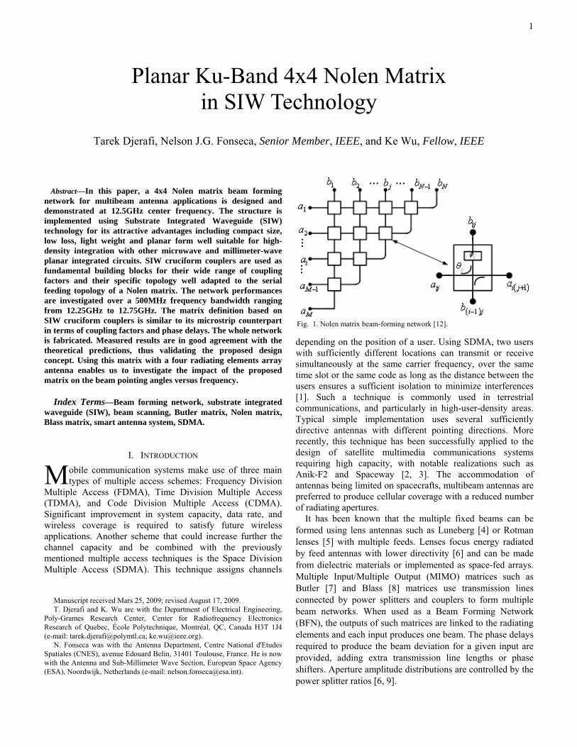
1
Abstract—In this paper, a 4x4 Nolen matrix beam forming network for multibeam antenna applications is designed and demonstrated at 12.5GHz center frequency. The structure is implemented using Substrate Integrated Waveguide (SIW) technology for its attractive advantages including compact size, low loss, light weight and planar form well suitable for high-density integration with other microwave and millimeter-wave planar integrated circuits. SIW cruciform couplers are used as fundamental building blocks for their wide range of coupling factors and their specific topology well adapted to the serial feeding topology of a Nolen matrix. The network performances are investigated over a 500MHz frequency bandwidth ranging from 12.25GHz to 12.75GHz. The matrix definition based on SIW cruciform couplers is similar to its microstrip counterpart in terms of coupling factors and phase delays. The whole network is fabricated. Measured results are in good agreement with the theoretical predictions, thus validating the proposed design concept. Using this matrix with a four radiating elements array antenna enables us to investigate the impact of the proposed matrix on the beam pointing angles versus frequency.
Index Terms—Beam forming network, substrate integrated waveguide (SIW), beam scanning, Butler matrix, Nolen matrix, Blass matrix, smart antenna system, SDMA.
I. INTRODUCTION
obile communication systems make use of three main types of multiple access schemes: Frequency Division
Multiple Access (FDMA), Time Division Multiple Access (TDMA), and Code Division Multiple Access (CDMA). Significant improvement in system capacity, data rate, and wireless coverage is required to satisfy future wireless applications. Another scheme that could increase further the channel capacity and be combined with the previously mentioned multiple access techniques is the Space Division Multiple Access (SDMA). This technique assigns channels
Manuscript received Mars 25, 2009; revised August 17, 2009. T. Djerafi and K. Wu are with the Department of Electrical Engineering,
Poly-Grames Research Center, Center for Radiofrequency Electronics Research of Quebec, École Polytechnique, Montréal, QC, Canada H3T 1J4 (e-mail: [email protected]; [email protected]). N. Fonseca was with the Antenna Department, Centre National d'Etudes Spatiales (CNES), avenue Edouard Belin, 31401 Toulouse, France. He is now with the Antenna and Sub-Millimeter Wave Section, European Space Agency (ESA), Noordwijk, Netherlands (e-mail: [email protected]).
depending on the position of a user. Using SDMA, two users with sufficiently different locations can transmit or receive simultaneously at the same carrier frequency, over the same time slot or the same code as long as the distance between the users ensures a sufficient isolation to minimize interferences [1]. Such a technique is commonly used in terrestrial communications, and particularly in high-user-density areas. Typical simple implementation uses several sufficiently directive antennas with different pointing directions. More recently, this technique has been successfully applied to the design of satellite multimedia communications systems requiring high capacity, with notable realizations such as Anik-F2 and Spaceway [2, 3]. The accommodation of antennas being limited on spacecrafts, multibeam antennas are preferred to produce cellular coverage with a reduced number of radiating apertures.
It has been known that the multiple fixed beams can be formed using lens antennas such as Luneberg [4] or Rotman lenses [5] with multiple feeds. Lenses focus energy radiated by feed antennas with lower directivity [6] and can be made from dielectric materials or implemented as space-fed arrays. Multiple Input/Multiple Output (MIMO) matrices such as Butler [7] and Blass [8] matrices use transmission lines connected by power splitters and couplers to form multiple beam networks. When used as a Beam Forming Network (BFN), the outputs of such matrices are linked to the radiating elements and each input produces one beam. The phase delays required to produce the beam deviation for a given input are provided, adding extra transmission line lengths or phase shifters. Aperture amplitude distributions are controlled by the power splitter ratios [6, 9].
Planar Ku-Band 4x4 Nolen Matrix in SIW Technology
Tarek Djerafi, Nelson J.G. Fonseca, Senior Member, IEEE, and Ke Wu, Fellow, IEEE
M
Fig. 1. Nolen matrix beam-forming network [12].
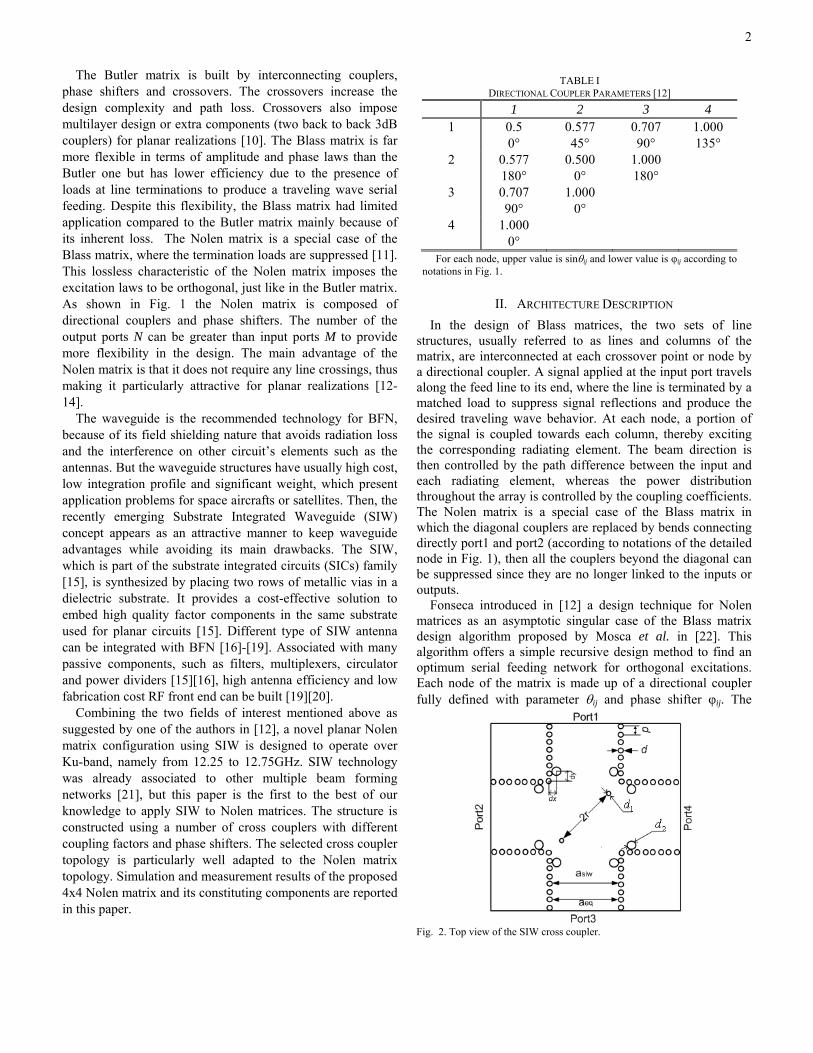
2
The Butler matrix is built by interconnecting couplers, phase shifters and crossovers. The crossovers increase the design complexity and path loss. Crossovers also impose multilayer design or extra components (two back to back 3dB couplers) for planar realizations [10]. The Blass matrix is far more flexible in terms of amplitude and phase laws than the Butler one but has lower efficiency due to the presence of loads at line terminations to produce a traveling wave serial feeding. Despite this flexibility, the Blass matrix had limited application compared to the Butler matrix mainly because of its inherent loss. The Nolen matrix is a special case of the Blass matrix, where the termination loads are suppressed [11]. This lossless characteristic of the Nolen matrix imposes the excitation laws to be orthogonal, just like in the Butler matrix. As shown in Fig. 1 the Nolen matrix is composed of directional couplers and phase shifters. The number of the output ports N can be greater than input ports M to provide more flexibility in the design. The main advantage of the Nolen matrix is that it does not require any line crossings, thus making it particularly attractive for planar realizations [12-14].
The waveguide is the recommended technology for BFN, because of its field shielding nature that avoids radiation loss and the interference on other circuit’s elements such as the antennas. But the waveguide structures have usually high cost, low integration profile and significant weight, which present application problems for space aircrafts or satellites. Then, the recently emerging Substrate Integrated Waveguide (SIW) concept appears as an attractive manner to keep waveguide advantages while avoiding its main drawbacks. The SIW, which is part of the substrate integrated circuits (SICs) family [15], is synthesized by placing two rows of metallic vias in a dielectric substrate. It provides a cost-effective solution to embed high quality factor components in the same substrate used for planar circuits [15]. Different type of SIW antenna can be integrated with BFN [16]-[19]. Associated with many passive components, such as filters, multiplexers, circulator and power dividers [15][16], high antenna efficiency and low fabrication cost RF front end can be built [19][20].
Combining the two fields of interest mentioned above as suggested by one of the authors in [12], a novel planar Nolen matrix configuration using SIW is designed to operate over Ku-band, namely from 12.25 to 12.75GHz. SIW technology was already associated to other multiple beam forming networks [21], but this paper is the first to the best of our knowledge to apply SIW to Nolen matrices. The structure is constructed using a number of cross couplers with different coupling factors and phase shifters. The selected cross coupler topology is particularly well adapted to the Nolen matrix topology. Simulation and measurement results of the proposed 4x4 Nolen matrix and its constituting components are reported in this paper.
II. ARCHITECTURE DESCRIPTION
In the design of Blass matrices, the two sets of line structures, usually referred to as lines and columns of the matrix, are interconnected at each crossover point or node by a directional coupler. A signal applied at the input port travels along the feed line to its end, where the line is terminated by a matched load to suppress signal reflections and produce the desired traveling wave behavior. At each node, a portion of the signal is coupled towards each column, thereby exciting the corresponding radiating element. The beam direction is then controlled by the path difference between the input and each radiating element, whereas the power distribution throughout the array is controlled by the coupling coefficients. The Nolen matrix is a special case of the Blass matrix in which the diagonal couplers are replaced by bends connecting directly port1 and port2 (according to notations of the detailed node in Fig. 1), then all the couplers beyond the diagonal can be suppressed since they are no longer linked to the inputs or outputs.
Fonseca introduced in [12] a design technique for Nolen matrices as an asymptotic singular case of the Blass matrix design algorithm proposed by Mosca et al. in [22]. This algorithm offers a simple recursive design method to find an optimum serial feeding network for orthogonal excitations. Each node of the matrix is made up of a directional coupler fully defined with parameter ij and phase shifter φij. The
TABLE I DIRECTIONAL COUPLER PARAMETERS [12]
1 2 3 4 1 0.5
0° 0.577 45°
0.707 90°
1.000 135°
2 0.577 180°
0.500 0°
1.000 180°
3 0.707 90°
1.000 0°
4 1.000 0°
For each node, upper value is sinij and lower value is φij according to notations in Fig. 1.
Fig. 2. Top view of the SIW cross coupler.
3
proposed design with 4 inputs and 4 outputs correspond to a 4x4 Butler matrix using 3dB/90° hybrid couplers. These parameters are used as entry into the Mosca et al. algorithm and the results were given in [12]. The theoretical parameters of directional couplers and phase shifters obtained for the matrix described above are reported in Table I.
The Nolen matrix consists of 3.01, 4.77 and 6.02dB couplers and phase shifters ranging from 45 to 180° compared to a reference line (0°). The SIW cross-coupler acts as the input and power delivery component instead of the conventional 90° or hybrid coupler. The Nolen matrix is designed at the center frequency of 12.5GHz with a 500MHz bandwidth. The topologies chosen for the design of various constituting elements of the matrix are presented in the next section.
A. SIW Cross Coupler
A standard H-plane coupler with a continuous coupling aperture over the entire width of the common broadside wall of two adjacent SIW waveguides may lead to coupling values varying between 3 and 5dB [23]. For a lower coupling factor multiple apertures must be used or two couplers must be cascaded at the expenses of the size and signal loss. The cruciform H-plane SIW coupler, proposed for the first time in SIW technology in [24], has the capability to achieve a wide range of coupling ratios while maintaining a very compact size since the coupling occurs in the crossing area of two simple SIW transmission lines as shown in Fig. 2. Furthermore, this perpendicular configuration is particularly adapted to Blass or Nolen matrices design according to the topology presented in Fig. 1.
From notations in Fig. 2, port 1 is the input port, port 2 is the coupling port, port 3 is the direct port and port 4 is the isolated port. aeq is the equivalent rectangular waveguide model width, set for proper behavior over targeted frequency range. Two posts are added in the crossing area to achieve the desired coupling; these posts have the same diameter 1d and
are diagonally separated by r. Two inductive posts are added in each port close to the crossing area in order to achieve a low return loss. The inductive matching posts have diameter d and position ,dx dy relative to a corner of the crossing area.
These parameters are adjusted to accomplish the desired coupling factor while minimizing S11 and S41.
The parameters are tuned using a three-dimensional (3-D) electromagnetic (EM) simulation software, High-Frequency
Structure Simulator (HFSS) by Ansoft, to achieve wide-band performances. A substrate with a relative permittivity of εr = 2.33 and a thickness of 0.787mm (RT/duroïd 5870) is used. Accordingly, the SIW characteristic dimensions are p = 1.524mm, d = 0.762mm and aeq = 13.35mm, where p is the distance between two successive posts and d is the diameter of the posts. The final dimensions of the needed SIW couplers are reported in Table II. As an example of performance demonstration, a 3dB coupler is fabricated and measured (Fig. 3). Microstrip to SIW transitions are placed at each ports of
TABLE II GEOMETRIC PARAMETERS OF DIRECTIONAL COUPLERS
3.01dB 4.77dB 6.02dB
1d (mm) 0.4 0.5 0.6
r (mm) 5.25 5.13 4.81
2d (mm) 0.8 0.8 0.8
dx (mm) 11.18 1.4 2.1
dy (mm) 1.44 1.16 1
(a)
(b)
Fig. 4. Simulation and measurement results for the H-plane SIW 3dB coupler: (a) S11 and S41 (b) S21 and S31 .
Fig. 3. S-parameters simulated result of the 3dB cross coupler.
4
the device for measurement purposes [25]. Simulation and measured results agree well in all the
waveguide bandwidth. The measured isolation and return loss are below 17dB in a bandwidth larger than 12-13GHz with a worst case value at 12GHz as shown in Fig. 4. In this bandwidth, ±0.5dB power equality is achieved in measurements (versus ±0.2dB in simulations). This slight degradation may be due in part to the feeding transitions for the measurement purpose. Fig. 5 compares the simulated and measured relative phase differences between direct and coupled ports. As shown in this figure, the relative phase difference is close to the theoretical -90° and has a worst case variation under 7° over the operating bandwidth in measurements.
The two other couplers were only simulated as the manufactured 3dB coupler proved good agreement with simulations and a coupling range compatible with the present need was already validated in [24]. For the 4.77dB coupler, the magnitude of S21 is 4.77dB with a ripple of 0.2dB from 12 to 13GHz and isolation below -17dB over the same bandwidth. For the 6.02dB coupler, the isolation is better than -18dB in the 12-13GHz frequency range with reflection below -15dB. The coupling factor offers good amplitude stability around the center frequency with a center value of 6.02dB and 0.2dB balance over the 12-13GHz frequency range.
B. SIW Nolen Matrix
In standard couplers as described in [23], the phase difference between the direct port and coupled port is +90°. The recursive relation in Mosca algorithm is derived using ideal directional coupler as shown in Fig. 1. The scattering matrix of the ideal directional couplers considered is:
0 sin cos 0
sin 0 0 cos
cos 0 0 sin
0 cos sin 0
ij ij
ij ij
ij ij
ij ij
j
jS
j
j
(1)
This leads to a phase difference between the direct port and the coupling port of -90°. This phase characteristic was verified by the microstrip branch line coupler as used in [12]. Interestingly, the proposed SIW cross coupler has the same phase characteristic. Then, one can use for this SIW design the same phase delays as used in microstrip technology. A broadside wall aperture coupler would have required adapting the phase delays to realize the proposed 4x4 matrix. Thus, it is noteworthy that the selected SIW cross coupler is well adapted to the Nolen matrix design process described by Fonseca in [12] and does not require to adapt the algorithm. Also, its geometry is particularly adapted to the Nolen or Blass matrix topologies, making this cross coupler the best choice for our design.
Combining the SIW couplers dimensioned in the previous section, a complete experimental SIW Nolen matrix has been constructed. To reduce the simulation time, the structure was initially designed using an equivalent rectangular waveguide model shown in Fig. 6. Additional SIW phase shifters are introduced to realize 45°, 90°, 135° and 180° phase delays optimized at the specified center frequency.
As illustrated in Fig. 6, phase shifts are done using either meander lines or waveguide cross section broad wall modification. In the first phase shifter technique, the lines are arranged in meanders in order to introduce a different phase-shift in each output port due to different electrical path lengths that allows one to produce a proper phase distribution in the array profile, while compensating the additional delay given by the routing. This meander is realised by connecting 90° bends. For reflection cancellation a via-hole element is added in each corner. The line must be properly routed in order to connect the coupler output to the next stage of the matrix. The
Fig. 5. Measured and simulated phase shifts between the outputs of coupler.
Fig. 6. Topology of SIW Nolen matrix in equivalent waveguide configuration.
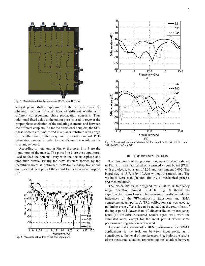
5
second phase shifter type used in the work is made by chaining sections of SIW lines of different widths with different corresponding phase propagation constants. Thus additional fixed delay at the output ports is used to recover the proper phase excitation of the radiating elements and between the different couplers. As for the directional couplers, the SIW phase shifters are synthesized in a planar substrate with arrays of metallic via by the easy and low-cost standard PCB fabrication process in order to manufacture the whole matrix in a unique board.
According to notations in Fig. 6, the ports 1 to 4 are the input ports of the matrix. The ports 5 to 8 are the output ports used to feed the antenna array with the adequate phase and amplitude profile. Finally the SIW structure formed by the metallized holes is optimized. SIW-to-microstrip transitions are placed at each port of the circuit for measurement purpose [25].
III. EXPERIMENTAL RESULTS
The photograph of the proposed eight-port matrix is shown in Fig. 7. It was fabricated on a printed circuit board (PCB) with a dielectric constant of 2.33 and loss tangent 0.002. The board size is 13.7cm by 10.5cm without the transitions. The via-holes were manufactured first by a mechanical process and then metalized.
The Nolen matrix is designed for a 500MHz frequency range operation around 12.5GHz. Fig. 8 shows the experimental return losses. The measured results include the influences of the SIW-microstrip transitions and SMA connectors at all ports. A TRL calibration set was used to minimize these effects. It can be noted that the return loss of the input ports is lower than -10 dB over the entire frequency band (12–13GHz). Measured results agree well with the simulated ones, except for the input port 4 where some performance degradation is observed. An essential criterion of a BFN performance for SDMA applications is the isolation between input ports, as it contributes to the level of interferences. Fig. 9 plots the results of the measured isolations, representing the isolations between
Fig. 7. Manufactured 4x4 Nolen matrix (13.7cm by 10.5cm).
Fig. 8. Measured return loss of the four input ports.
(a)
(b)
Fig. 9. Measured isolation between the four input ports: (a) S21, S31 and S41, (b) S32, S42 and S43
6
each couple of input ports (S21, S31, S41, S32, S42 and S43) of the proposed Nolen matrix. Over the entire operating frequency band, the isolation level is lower than -12 dB. The isolation between port1 and port2 is below -19dB over the working frequency range and below -15dB over an extended 12-13GHz band. In simulations, these results are about 5dB lower. The worst case both in measurement and simulation is related to the isolation between ports 2 and 3. Depending on
the application (electronically controlled beam, SDMA in both transmit and receive systems), system analyses are needed to evaluate the impact of isolation on the global system performances. Fig.10 presents the simulated mean transmission coefficient for each input port and Fig. 11 the measured means values. Good agreement is found between simulations and measurements over the nominal 500MHz operating frequency range. Transmission coefficients are well equalized and are close to the theoretical predicted value of -6dB with an average value of -6.5dB. The maximum error is less than ±0.5dB in simulations and around ±1dB in measurements. Line losses in the dielectric are estimated to be around 0.75dB. But this value varies with the electrical path length: the shorter one (1 towards 5) presents lower losses while the longer one (4 towards 8) has line losses around 1.2dB. The performances also of the first path have wider bandwidth behavior than the longer one. Furthermore, measured results degrade faster outside the operating band than predicted in simulations. The possible sources of loss in an SIW structure are: conductor losses due to the finite conductivity of the metal walls, dielectric losses due to the loss tangent of the dielectric material and radiation losses due to the presence of the slots in the side walls. The dielectric loss may cause the major part of the attenuation. The radiations are very small
Fig. 12. Simulated and measured relative phase differences between adjacent output ports for port1.
Fig. 10. Simulated means of the transmissions coefficients amplitude for each input port.
Fig. 11. Measured means of the transmissions coefficients amplitude for each input port.
TABLE III PHASE DIFFERENCE ON TRANSMISSION COEFFICIENTS (SIMULATED/MEASURED)
Phase6-
phase5(degree) Phase7-
phase6(degree) Phase8-
phase7(degree)
Port Frequency(GHz
) 12 12.5 12.75 12 12.5 12.75 12 12.5 12.75
1 Simulated -33.17 -44.4 -63.2 -23.1 -44.1 -59.9 -17.5 -38.5 -63.6 Measured -22.2 -43. 5 -63.8 -25.6 -39.4 -58.2 -16.8 -42.8 -72.2
2 Simulated 145.0 129.5 111.9 148.3 131.9 109.8 151.2 146.3 124.1 Measured 163 142.2 118.9 147.2 135.5 108.0 158.2 133.1 114.3
3 Simulated 60.3 34.0 22.0 78.4 52.0 31.9 63.6 46.3 20.7 Measured 61.65 46.39 31.6 60.74 47.85 19.17 81.98 50.14 36.22
4 Simulated -131.1 -143.9 -159.0 -108.2 -130.0 -148.4 -103.9 -133.6 -152.3Measured -118.1 -129.9 -150.9 -115.7 -136.3 -156.4 -105.8 -136.8 -147.8
7
and in fact completely negligible when the metal via dimension and space are adequately selected.
The observed shift between simulations and measurements may be related to the SIW-microstrip transitions and fabrication errors. Especially, it must be mentioned that the mechanical and chemical processes developed at our Poly-GRAMES laboratory and used respectively to make the holes and metalize them are at the limit with the required dimensions of this circuit.
Fig. 12 compares simulation and measurement transmission phases for the port 1 of the proposed matrix. It is found that the simulated and measured results are in good agreement and the transmission phase coefficients are close to the theoretical values over the operating frequency band.
Similar performances were found for the other input ports. The values of the phase difference of all the input port are reported in Table III at 12.25, 12.5 and 12.75GHz. At the center frequency (12.5GHz), the measured means phase differences are respectively (-41.85, 136.93, 48.13, -134.08) compared to the optimized ones (-42.3, 131.09, 44.12, -135.82) and the theoretical ones (-45, 135, 45, -135) ranging from port 1 to port 4, respectively. Compared with the simulated results, the measurement results have some phase shift, which may be mainly due to the connectors. The achieved results are all in good agreement with a worst case error of 7° over the operating bandwidth.
The frequency-dependent phase behavior of this matrix was expected and is due to the serial feeding characterizing a Blass or Nolen matrix. In fact, the incremental phase shift between adjacent outputs varies with frequency. For instance as shown in Table III, when the first input is used over the bandwidth f0±0.25GHz, the phase difference between adjacent outputs
changes by ±20°. This gradient for each output can be used to control the beam squint effect, as investigated in [14]. To evaluate the impact of the proposed matrix on beam squint and compare it with its microstrip counterpart in S-Band [14], the measured Nolen matrix is used to feed a 4-element linear array with a spacing defined at center frequency of 0.63λ0. A square patch is used as array element; the radiation pattern is given as qcos , with 2.1q . Fig. 13 shows the array
patterns in polar coordinates produced by the four inputs, each pointing in direction
0 depending on the phase difference
between adjacent ports. These parameters are linked by
the following formula:
00 sin d (2)
where 0 is the angular wave number in free space and d the
distance between two radiating elements. Let us first evaluate the beam squint of the four beams over the operational bandwidth, i.e. 12.25-12.75GHz. For port1, the beam pointing is 0 = -9.9° at the center frequency, and
over the targeted bandwidth, the main beam scans from -5.3° to -15.3°. In comparison to the gain at center frequency, the beam squint effect induces a gain drop around 0.2 dB, which remains acceptable for most applications. For port 2, the beam squint is 9.6° varying from 28.7° to 38.3 °. For port 3, it scans from 6.9° to 16.2° with center frequency beam pointing at 11.5°. For port 4, it scans from -27.7° to -40.7°. Then, one may note that the beam squint is quite similar for all beams. In fact, the bandwidth analyzed being relatively small (4%), the beam squint due to the linear array is negligible compared to the beam squint introduced by the matrix. To compare this matrix with the microstrip one realized in S-band, we
0.2 0.4
0.6 0.8 1
60
30
0
-30
-60
-90 90
a)
0.2 0.4
0.6 0.8 1
60
30
0
-30
-60
-90 90
b)
0.2 0.4
0.6 0.8 1
60
30
0
-30
-60
-90 90
c)
0.2 0.4
0.6 0.8 1
60
30
0
-30
-60
-90 90
d)
Fig. 13. Simulation H plane radiation patterns versus frequency of a 4-patch array fed by the designed Nolen matrix for a) port1, b) port2, c) port3, d) port4
8
investigate the beam squint over similar bandwidths: 12-13GHz in Ku-band leading to an 8% relative bandwidth to be compared with 9% (2.1-2.3GHz) in S-band. In Ku-band with 1GHz bandwidth, the beam squint is around 20° and is very similar for all ports (from 0° to 20° for port 1, from -44° to -25.2° for port 2, from -21.8° to -2.3° for port 3 and from 22° to 43.1° for port 4, the first values for each port being at 12GHz and the second at 13GHz). In S-band over a similar relative bandwidth, the beam squint is much smaller and depends more on the input port. From 2.1 to 2.3GHz, the beams scan from 7 to 15°, from -39 to -27°, from -14 to -7° and from 31 to 35° for ports 1 to 4, respectively. This is understood by the fact that electrical paths are smaller in the microstrip realization, which reduces the phase dispersion induced by the matrix. Further investigations are needed on the proposed SIW concept to evaluate the possibility to reduce electrical paths and reach improved performances in terms of beam squint. For narrow band applications, the presented performances may be acceptable. If higher constraints are defined on the beam pointing accuracy, this may require selecting another technology. Still this has to be put in balance with the advantages brought by the SIW technology such as lower coupling, lower line losses, etc.
IV. CONCLUSION
A Nolen matrix based on SIW technology has been proposed and validated experimentally for the first time. The matrix is optimized using the commercial software HFSS and fabricated to operate from 12.25 to 12.75GHz. 3.01dB, 4.77dB and 6.02dB SIW cross couplers are designed as well as different phase shifters to build a complete 4x4 Nolen matrix. The measured power-split unbalance stays within 0.5dB over the design bandwidth. The relative phase difference distribution is used to estimate the variation of the beam pointing angle over the bandwidth. The proposed SIW design has the advantage of low cost, low profile, light weight, high integration density, and ease of fabrication. We also expect this design to reduce line losses when compared to its microstrip counterpart.
Further investigations are in process to fully compare SIW and microstrip technologies for MIMO matrices. In this comparison, the power handling is also planned to be addressed as it is a real concern in radiofrequency communication systems. It will be of interest to evaluate how SIW compares to other technologies and mainly standard waveguide technology in this regard.
REFERENCES [1] C. Godara, “Application of antenna arrays to mobile
communications, Part I: Performance improvement, feasibility and system considerations,” Proc. IEEE, vol. 85, pp. 1029–1070, July 1997.
[2] D. Le Doan, E. Amyotte, C. Mok and J. Uher, “Anik-F2 Ka-Band Transmit Multibeam Antenna,” Proc. ANTEM2004, Canada, 2004.
[3] http://www.boeing.com/defense-space/space/bss/factsheets/702/spaceway/spaceway.html
[4] R.K. Luneberg, Mathematic Theory of Optics, Brown University Press, pp. 189-212, 1944.
[5] W. Rotman and R. Turner, “Wide-Angle Microwave Lens for Line Source Applications,” IEEE trans. on Antennas and Propagation, Vol. 11, Issue 6, pp. 623-632, Nov. 1963.
[6] Y. T. Lo and S. W. Lee, antenna handbook: theory, applications, and design, Van Nostrand Reinhold, 1988.
[7] J. Butler and R. Lowe, “Beam-Forming Matrix Simplifies Design of Electronically Scanned Antennas,” Electronic Design, pp. 170-173, April 1961.
[8] J. Blass, “Multidirectionnal Antenna, a New Approach to Stacked Beams,” IRE International Conf. record, V. 8, Part 1, pp. 48-50, 1960.
[9] P.S. Hall and S.J. Vetterlein, “Review of radio frequency beamforming techniques for scanned and multiple beam antennas,” IEE Proceedings H Microwaves, Antennas and Propagation, V. 137, I. 5, pp.293-303, Oct. 1990.
[10] S. Yamamoto, J. Hirokawa, and M. Ando, “A beam switching slot array with a 4-way Butler matrix installed in single layer post-wall waveguides,” IEICE Trans. Commun., V.E86-B, no.5, pp.1653–1659, May 2003.
[11] J. Nolen, Synthesis of Multiple Beam Networks for Arbitrary Illuminations, PhD Thesis, Bendix Corporation, Radio Division, Baltimore, April 1965.
[12] N.J.G. Fonseca, “Study and Design of a S-band 4x4 Nolen Matrix for Satellite Digital Multimedia Broadcasting Applications,” 12th International Symp. ANTEM URSI Montreal (QC), July 16-19 2006, pp. 481-484.
[13] N.J.G Fonseca, Etude des Matrices de Blass et Nolen, CNES Technical Note n°152, 98 pages, Nov. 2007. Available online at http://cct/cct13/infos/notestech.htm
[14] N.J.G Fonseca, “Printed S-Band 4x4 Nolen Matrix for Multiple Beam Antenna Applications”, IEEE Trans. on Antennas and Propagation, Vol. 57, Issue 6, pp. 1673-1678, Jun. 2009.
[15] K. Wu, “Integration and interconnect techniques of planar and nonplanar structures for microwave and millimeter-wave circuits—Current status and future trend,” in 2001 Asia–Pacific Microwave Conf., Taipei,Taiwan, R.O.C., Dec. 3–6, 2001, pp. 411–416.
[16] W. Hong, “Development of microwave antennas, components and subsystems based on SIW technology,” IEEE International Symposium on Microwave, Antenna, Propagation and EMC Technologies for Wireless Communications, MAPE 2005, Vol.1, pp.14–17 .
[17] J.Z. Peng,, S.Q. Xiao, X.J. Tang, and J.C. Lu, “A Novel Ka-band Wideband Slot Antenna for System-on-Package Application,” Journal of Electromagnetic Waves and Applications, Vol. 22, pp. 1705-1712, Dec. 2008.
[18] Z. C. Hao,W. Hong, J. X. Chen, X. P. Chen, and K.Wu, “A novel feeding technique for antipodal linearly tapered Slot Antenna Array,” Dig. In IEEE MTT-S Long Beach, CA, Jun. 2005, pp. 1641–1643.
[19] D. Stephens, P. R. Yong, and I. D. Robertson, “W-band substrate integrated waveguide slot antenna,” Electron. Lett., vol. 41, pp. 165–167, Feb. 2005.
[20] R. V. Gatti, L. Marcaccioli, E. Sbarra. and R.Sorrentino, “Flat Array Antennas for Ku-Band Mobile Satellite Terminals,” International Journal of Antennas and Propagation,ID 836074, Feb. 2009.
[21] Y.J. Cheng, W. Hong K. Wu, Z.Q. Kuai, Y. Chen, J.X. Chen, J.Y. Zhou and H.J. Tang, “Substrate Integrated Waveguide (SIW) Rotman Lens and Its Ka-Band Multibeam Array Antenna Applications,” IEEE Transactions On Antennas and Propagation, Vol. 56, Issue: 8, Part 2, pp. 2504-2513, Aug. 2008.
[22] Mosca, S. Bilotti, F. Toscano. A et Vegni, L. 2002. A Novel Design Method for Blass Matrix Beam-Forming Networks. IEEE Trans. Antennas and Propagation, Vol. 50, No. 2, pp 225-232.
[23] Y. Cassivi, D. Deslandes and K. Wu, “Substrate Integrated Waveguide Directional Couplers,” Asia-Pacific Microwave Conference Proceedings.
[24] T. Djerafi and K. Wu, “Super-compact substrate integrated waveguide cruciform directional coupler,” IEEE Microw.Wireless Compon. Lett., vol. 17, no.11, pp. 757-759, Nov.2007.
[25] D. Deslandes and K. Wu, “Integrated Microstrip and Rectangular Waveguide in Planar Form,”. IEEE Microwave and Wireless Components Letters. Vol. 11. No. 2. pp. 68-70. February 2001.

93
ARTICLE V: BROADBAND SUBSTRATE INTEGRATED WAVEGUIDE
NOLEN MATRIX BASED ON COUPLER DELAY COMPENSATION
Tarek Djerafi, Nelson J.G. Fonseca, et Ke Wu
Article accepté avril 2011 dans IEEE Transactions on Microwave Theory and Techniques.
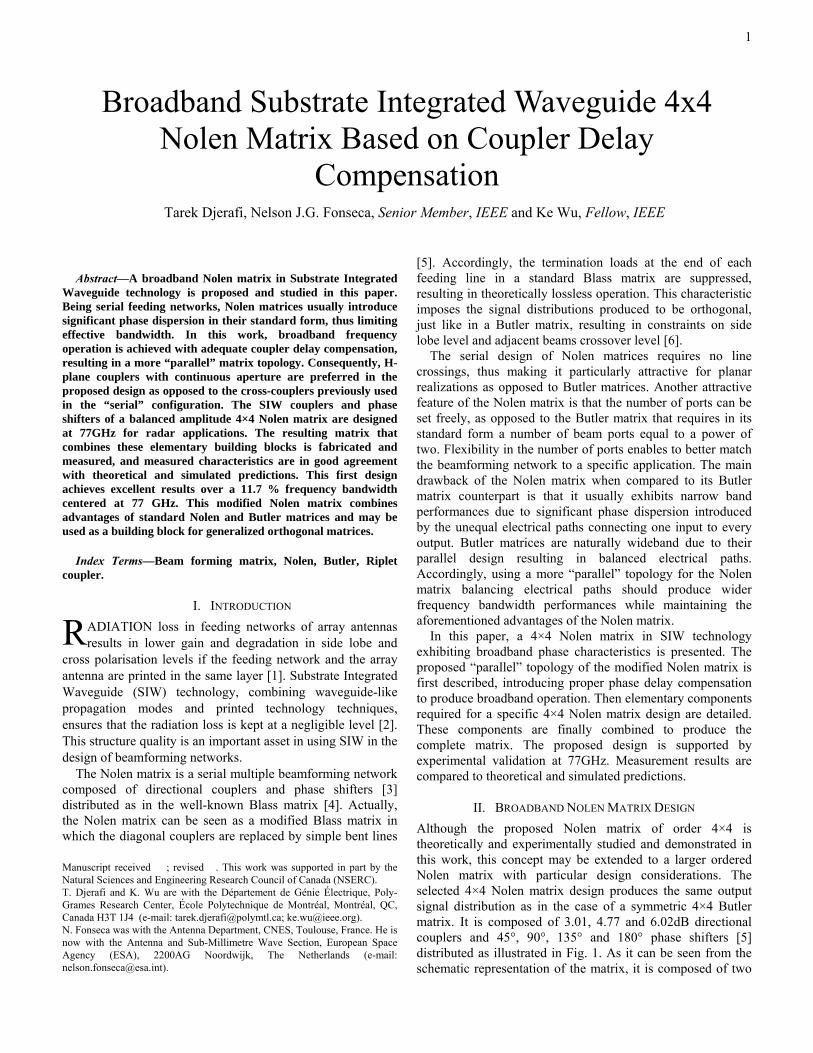
1
Abstract—A broadband Nolen matrix in Substrate Integrated
Waveguide technology is proposed and studied in this paper. Being serial feeding networks, Nolen matrices usually introduce significant phase dispersion in their standard form, thus limiting effective bandwidth. In this work, broadband frequency operation is achieved with adequate coupler delay compensation, resulting in a more “parallel” matrix topology. Consequently, H-plane couplers with continuous aperture are preferred in the proposed design as opposed to the cross-couplers previously used in the “serial” configuration. The SIW couplers and phase shifters of a balanced amplitude 4×4 Nolen matrix are designed at 77GHz for radar applications. The resulting matrix that combines these elementary building blocks is fabricated and measured, and measured characteristics are in good agreement with theoretical and simulated predictions. This first design achieves excellent results over a 11.7 % frequency bandwidth centered at 77 GHz. This modified Nolen matrix combines advantages of standard Nolen and Butler matrices and may be used as a building block for generalized orthogonal matrices.
Index Terms—Beam forming matrix, Nolen, Butler, Riplet coupler.
I. INTRODUCTION
ADIATION loss in feeding networks of array antennas results in lower gain and degradation in side lobe and
cross polarisation levels if the feeding network and the array antenna are printed in the same layer [1]. Substrate Integrated Waveguide (SIW) technology, combining waveguide-like propagation modes and printed technology techniques, ensures that the radiation loss is kept at a negligible level [2]. This structure quality is an important asset in using SIW in the design of beamforming networks.
The Nolen matrix is a serial multiple beamforming network composed of directional couplers and phase shifters [3] distributed as in the well-known Blass matrix [4]. Actually, the Nolen matrix can be seen as a modified Blass matrix in which the diagonal couplers are replaced by simple bent lines Manuscript received ; revised . This work was supported in part by the Natural Sciences and Engineering Research Council of Canada (NSERC). T. Djerafi and K. Wu are with the Département de Génie Électrique, Poly-Grames Research Center, École Polytechnique de Montréal, Montréal, QC, Canada H3T 1J4 (e-mail: [email protected]; [email protected]). N. Fonseca was with the Antenna Department, CNES, Toulouse, France. He is now with the Antenna and Sub-Millimetre Wave Section, European Space Agency (ESA), 2200AG Noordwijk, The Netherlands (e-mail: [email protected]).
[5]. Accordingly, the termination loads at the end of each feeding line in a standard Blass matrix are suppressed, resulting in theoretically lossless operation. This characteristic imposes the signal distributions produced to be orthogonal, just like in a Butler matrix, resulting in constraints on side lobe level and adjacent beams crossover level [6].
The serial design of Nolen matrices requires no line crossings, thus making it particularly attractive for planar realizations as opposed to Butler matrices. Another attractive feature of the Nolen matrix is that the number of ports can be set freely, as opposed to the Butler matrix that requires in its standard form a number of beam ports equal to a power of two. Flexibility in the number of ports enables to better match the beamforming network to a specific application. The main drawback of the Nolen matrix when compared to its Butler matrix counterpart is that it usually exhibits narrow band performances due to significant phase dispersion introduced by the unequal electrical paths connecting one input to every output. Butler matrices are naturally wideband due to their parallel design resulting in balanced electrical paths. Accordingly, using a more “parallel” topology for the Nolen matrix balancing electrical paths should produce wider frequency bandwidth performances while maintaining the aforementioned advantages of the Nolen matrix. In this paper, a 4×4 Nolen matrix in SIW technology exhibiting broadband phase characteristics is presented. The proposed “parallel” topology of the modified Nolen matrix is first described, introducing proper phase delay compensation to produce broadband operation. Then elementary components required for a specific 4×4 Nolen matrix design are detailed. These components are finally combined to produce the complete matrix. The proposed design is supported by experimental validation at 77GHz. Measurement results are compared to theoretical and simulated predictions.
II. BROADBAND NOLEN MATRIX DESIGN
Although the proposed Nolen matrix of order 4×4 is theoretically and experimentally studied and demonstrated in this work, this concept may be extended to a larger ordered Nolen matrix with particular design considerations. The selected 4×4 Nolen matrix design produces the same output signal distribution as in the case of a symmetric 4×4 Butler matrix. It is composed of 3.01, 4.77 and 6.02dB directional couplers and 45°, 90°, 135° and 180° phase shifters [5] distributed as illustrated in Fig. 1. As it can be seen from the schematic representation of the matrix, it is composed of two
Tarek Djerafi, Nelson J.G. Fonseca, Senior Member, IEEE and Ke Wu, Fellow, IEEE
Broadband Substrate Integrated Waveguide 4x4 Nolen Matrix Based on Coupler Delay
Compensation
R
2
sets of lines, usually referred to as feeding rows and columns of the matrix, which are interconnected at each cross-over point by a
directional coupler combined with a phase shifter. The top row or feeding line 1 of the matrix is actually a simple serial feeding network. The design of the other rows, or feeding lines with index higher than 1, is more complicated due to the coupling between one given feeding line and those of lower index. Interestingly, as demonstrated in [5], a Blass matrix design algorithm can be also used to design Nolen matrices. A first design of Nolen matrix in SIW technology was proposed by the authors in [7] and [8] without at that time paying particular attention to the phase dispersion over frequency, the main target being to propose a compact design for narrow band applications. This was achieved through the use of cross-couplers with shape and ports distribution that is particularly well adapted to the general topology of the Nolen matrix. The same topology cross coupler is proposed in two layer version in [9]. To achieve wide band performances, the components of the Nolen matrix are distributed in a more “parallel” topology as illustrated in Fig. 2. Parallel couplers are then preferred for this design, as they are more adapted to the new topology. In Fig. 2, the different paths between port 1 and the output ports (labeled 5 to 8) are highlighted. The signal directed toward port 7 and port 8 passes through the 6.02, 4.77 and 3.01dB couplers, in the order they are encountered. The signal
directed toward port 6 passes through the 6.02 and 4.77dB couplers only. The insertion phase of the 3.01dB coupler direct port, noted φ1, must be compensated toward ports 5 and 6 for wide band operation. The corresponding phase shifter is then added before output port 6. Similarly, the electrical path between ports 1 and 5 requires a phase delay compensation, noted φ2, corresponding to the insertion phase introduced by the 4.77dB coupler direct port, in addition to the φ1 delay already required because of the 3.01dB coupler. Accordingly, two phase shifters are cascaded before the output port 5, as illustrated in Fig. 2. Similarly, additional phase shifts are required for proper wide band operation of the other input ports and they are detailed in Fig. 2. They are in addition to the phase shifters normally required by the standard Nolen matrix topology (with numerical values in Fig. 2). The building blocks for this topology are detailed below. They are designed on the Rogers 6002 substrate, with loss tangent of 0.0012, relative permittivity of 2.94 and 0.508mm of thickness.
A. Design of the directional coupler
As already discussed, H-plane couplers, also known as short-slot Riblet couplers, with three different coupling values are required for the proposed Matrix topology. In SIW technology, this coupler can achieve 15% bandwidth for the 3.01dB coupling value [10][11]. Fig. 3 shows the configuration of the waveguide directional coupler with matched H-plane impedance steps [12]. Port 1 is input 1, port 2 the direct output, port 3 the coupled and port 4 the isolated. A full-wave commercial software (HFSS) is used to optimize the three different couplers needed. To prevent propagation of the undesired TE30 mode, impedance steps are used. Parameter values for the three different designs are listed in Table I.
TABLE I
DIMENSIONS OF THE SHORT SLOT COUPLER (mm) Parmeters 3.01dB 4.77dB 6.02dB
a 1.700 1.7 1.7 a1 1.62 1.608 1.642 a2 1.565 1.475 1.389 a3 1.313 1.475 1.389 L 2.33 3.4 3.486 L1 1.148 0 0 L2 2.182 1.06 1.42
L3 4.242 4.428 4.58
Simulation results of the three different couplers over the
frequency range of 70-82GHz as provided by HFSS are
135°
90°
45°
90°
180°
180°
φ1
φ2
φ1φ2
φ2
1
2
3
4
5
6
7
83.01dB
4.77dB
6.02dB
3.01dB6.02dB
4.77dB
Fig. 2. Proposed Nolen matrix beam-forming network. φ1and φ2, corresponding to the insertion phase introduced by the 3.01 and 4.77dBcouplers.
1a
2a
1Ma
Ma
1b 2b 1Nb Nb
ia
jb
ij
ijija 1jia
1jib
ijb
1
2
3
4
Fig. 1. Nolen matrix beam-forming network [3, 5].
Fig. 3. Topology of the H-plane short-slot coupler.
3
reported in Fig. 4. A coupling of 3.18±0.1dB is achieved between 70 and 80GHz for the balanced coupler. Over this frequency band, isolation and return loss are greater than 25dB. For the 4.77dB coupler, the coupling value varies between 4.70dB (reached at 76GHz) and 5.08dB (reached at 80GHz). The return loss and the isolation are greater than 20dB over the 70-80GHz frequency range. Finally, for the 6.02dB coupler, the coupling coefficient varies from -6.3dB (reached at 77GHz) and -6.64dB (reached at 80GHz). The simulated phase difference between the coupled and direct ports is around the theoretical value of 90° with a worst case error of 1.5° over the 70-80GHz frequency band. Based on the energy conservation, the loss is estimated around 0.2dB for the designed couplers.
B. Phase shifter
The phase shift can be realised by the use of unequal-length equal-width transmission lines, resulting in phase shift φ β l , where β is the wave number and Δl the
length difference, or the use of equal-length unequal-width transmission lines, resulting in phase shift φ β l , where l
is the length of the transmission lines and Δβ the wave number difference due to the width difference. In this design, we make use of phase shifters combining both characteristics: unequal–length unequal–width transmission lines, producing phase shift 1 1 2 2φ β l β l [13]. The topology of the phase shifter
is shown in Fig. 5. The optimized dimensions of the 45° phase shifter are: ∆a=0.1mm, ls=1.9mm and ∆l=0.4mm. Fig. 6 shows the simulated reflection coefficient and phase shift of the optimized phase shifter with HFSS. The designed phase shifter provides a differential phase shift of 45+0.4°, together with a reflection coefficient less than -20dB over the wide frequency range of consideration. To achieve 90° phase shift, the same topology is used with 2∆l and 2ls. Appropriate integer multiples are used in the same manner to achieve the 135 and 180° phase shifts.
C. Phase compensation
As shown in Fig. 7 there is a phase delay between the direct path of the 4.77dB coupler and a reference transmission line with the same length and width. The insertion phase of the couplers’ direct port, required for a phase delay compensation as defined in the beginning of Section II, are for the proposed design φ1= -15.7°, φ2=-53.2° , these values being given at 77GHz.
To compensate this delay, a simple SIW line is used with larger width and longer length following the principle of the
Fig. 6. Return loss and phase difference of the 45° phase shifter as shown in Fig.5 with ∆a=0.1 mm, ls=1.9mm and ∆l=0.4mm.
(a)
(b)
(c) Fig. 4. S-parameters of the optimized H-plane couplers shown in Fig. 3 with Table I parameters, Isolation, return loss, transmission coefficient and simulated phase shift difference between the direct and coupled ports for (a) the 3.01dB coupler, (b) the 4.77dB coupler and (c) the 6.02dB coupler.
a l
sl
Fig. 5. Topology of unequal with unequal length phase shifter
4
phase shifter described in Section B and illustrated in Fig. 5 (unequal–length unequal–width). For the 4.77dB coupler, a line with a width of 1.75mm and an additional length of 0.32mm compared to the coupler’s direct port length of 6mm is used. Fig. 8 shows the initial variation of this phase difference versus frequency without compensation: the phase changes from -52 to -57° over the 70 to 82GHz frequency range. With compensation, the phase difference is almost 0°. This result illustrates the capability of the phase shifter to not only correct absolute phase value but also phase variation over a relatively wide frequency range.
When applicable, cascaded phase shifters in Fig. 2, including standard Nolen matrix phase shifters and couplers’ delay compensation phase shifters may be combined by simply adding the proper parameters, namely ls and ∆l.
III. EXPERIMENTAL VALIDATION
Six H-plane couplers and eight phase shifters are connected together according to the topology described in Fig. 2 to build a planar eight port structure. When necessary, meander lines are used to maintain a “parallel” topology for the main feeding lines. The complete matrix was implemented on a dielectric substrate with laser micro-machining technique, which can perforate any type of shape. Metallic coating was then used to produce conductive vertical walls, characteristics of SIW technology. The photograph of the fabricated 8-port junction is shown in Fig. 9. The input and output ports are separated to allow the measurements, but an equal-length section is added at the output ports to preserve the phase shifting characteristics. The main functional area is 6cm×1cm without the added sections to separate the ports. A simple multi-step transition toward the standard WR10 waveguide cross-section is used for measurements.
Fig. 10 shows the simulated and measured reflection coefficients of input port 1 and the isolation between this port and the other input ports. The return loss is greater than 19dB over the frequency range in the simulation and greater than 10dB in the measurement. The isolation between port 1 and the other input ports is greater than 15dB over the frequency band from 72 to 81GHz. As presented in Fig. 11, the simulated transmission coefficients are well equalized around -6.7dB and are close to
Fig. 8. Phase difference between the coupler and the SIW line equivalent length without and with compensation
Fig. 7. Simulated E-field magnitude distributions obtained by HFSS at77GHz, along the 4.77 dB coupler and a SIW line with the same length.
(a)
(b)
Fig. 10. (a) Simulated and (b) measured return losses and isolations of the designed Nolen matrix fed at port 1.
Fig. 9. Manufactured 4×4 Nolen matrix at 77GHz.
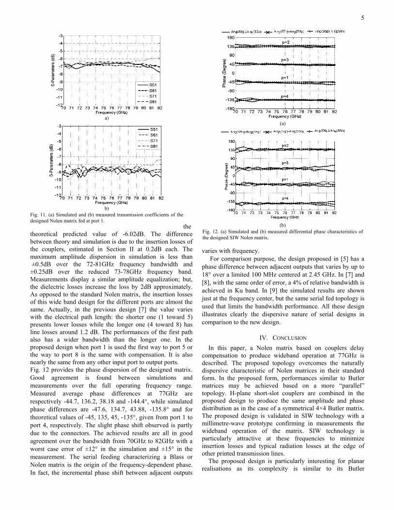
5
the theoretical predicted value of -6.02dB. The difference between theory and simulation is due to the insertion losses of the couplers, estimated in Section II at 0.2dB each. The maximum amplitude dispersion in simulation is less than ±0.5dB over the 72-81GHz frequency bandwidth and ±0.25dB over the reduced 73-78GHz frequency band. Measurements display a similar amplitude equalization; but, the dielectric losses increase the loss by 2dB approximately. As opposed to the standard Nolen matrix, the insertion losses of this wide band design for the different ports are almost the same. Actually, in the previous design [7] the value varies with the electrical path length: the shorter one (1 toward 5) presents lower losses while the longer one (4 toward 8) has line losses around 1.2 dB. The performances of the first path also has a wider bandwidth than the longer one. In the proposed design when port 1 is used the first way to port 5 or the way to port 8 is the same with compensation. It is also nearly the same from any other input port to output ports. Fig. 12 provides the phase dispersion of the designed matrix. Good agreement is found between simulations and measurements over the full operating frequency range. Measured average phase differences at 77GHz are respectively -44.7, 136.2, 38.18 and -144.4°, while simulated phase differences are -47.6, 134.7, 43.88, -135.8° and for theoretical values of -45, 135, 45, -135°, given from port 1 to port 4, respectively. The slight phase shift observed is partly due to the connectors. The achieved results are all in good agreement over the bandwidth from 70GHz to 82GHz with a worst case error of ±12° in the simulation and ±15° in the measurement. The serial feeding characterizing a Blass or Nolen matrix is the origin of the frequency-dependent phase. In fact, the incremental phase shift between adjacent outputs
varies with frequency. For comparison purpose, the design proposed in [5] has a
phase difference between adjacent outputs that varies by up to 18° over a limited 100 MHz centered at 2.45 GHz. In [7] and [8], with the same order of error, a 4% of relative bandwidth is achieved in Ku band. In [9] the simulated results are shown just at the frequency center, but the same serial fed topology is used that limits the bandwidth performance. All these design illustrates clearly the dispersive nature of serial designs in comparison to the new design.
IV. CONCLUSION
In this paper, a Nolen matrix based on couplers delay compensation to produce wideband operation at 77GHz is described. The proposed topology overcomes the naturally dispersive characteristic of Nolen matrices in their standard form. In the proposed form, performances similar to Butler matrices may be achieved based on a more “parallel” topology. H-plane short-slot couplers are combined in the proposed design to produce the same amplitude and phase distribution as in the case of a symmetrical 4×4 Butler matrix. The proposed design is validated in SIW technology with a millimetre-wave prototype confirming in measurements the wideband operation of the matrix. SIW technology is particularly attractive at these frequencies to minimize insertion losses and typical radiation losses at the edge of other printed transmission lines.
The proposed design is particularly interesting for planar realisations as its complexity is similar to its Butler
a)
b)
Fig. 11. (a) Simulated and (b) measured transmission coefficients of the designed Nolen matrix fed at port 1.
(a)
(b)
Fig. 12. (a) Simulated and (b) measured differential phase characteristics of the designed SIW Nolen matrix.
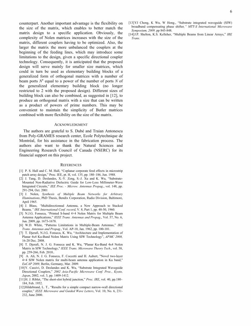
6
counterpart. Another important advantage is the flexibility on the size of the matrix, which enables to better match the matrix design to a specific application. Obviously, the complexity of Nolen matrices increases with the size of the matrix, different couplers having to be optimized. Also, the larger the matrix the more unbalanced the couplers at the beginning of the feeding lines, which may introduce some limitations to the design, given a specific directional coupler technology. Consequently, it is anticipated that the proposed design will serve mainly for smaller size matrices, which could in turn be used as elementary building blocks of a generalized form of orthogonal matrices with a number of beam ports Nn equal to a power of the number of ports N of the generalized elementary building block (no longer restricted to 2 with the proposed design). Different sizes of building block can also be combined, as suggested in [12], to produce an orthogonal matrix with a size that can be written as a product of powers of prime numbers. This may be convenient to maintain the simplicity of Butler matrices combined with more flexibility on the size of the matrix.
ACKNOWLEDGMENT
The authors are grateful to S. Dubé and Traian Antonescu from Poly-GRAMES research center, Ecole Polytechnique de Montréal, for his assistance in the fabrication process. The authors also want to thank the Natural Sciences and Engineering Research Council of Canada (NSERC) for its financial support on this project.
REFERENCES [1] P. S. Hall and C. M. Hall, “Coplanar corporate feed effects in microstrip
patch array design,” Proc. IEE, pt. H, vol. 135, pp. 180–186, Jun. 1988. [2] J. Tang, D. Deslandes, X.-Y. Zeng, S.-J. Xu and K. Wu, “Substrate-
Mounted Non-Radiative Dielectric Guide for Low-Loss Millimeter-Wave Integrated Circuits,” IEE Proc. - Microw. Antennas Propag., vol. 148, pp. 291-294, Oct. 2001
[3] J. Nolen, Synthesis of Multiple Beam Networks for Arbitrary Illuminations, PhD Thesis, Bendix Corporation, Radio Division, Baltimore, April 1965.
[4] J. Blass, “Multidirectionnal Antenna, a New Approach to Stacked Beams,” IRE International Conf. record, V. 8, Part 1, pp. 48-50, 1960.
[5] N.J.G. Fonseca, “Printed S-band 4×4 Nolen Matrix for Multiple Beam Antenna Applications,” IEEE Trans. Antennas and Propag., Vol. 57, No. 6, Jun. 2009, pp. 1673-1678.
[6] W.D. White, “Patterns Limitations in Multiple-Beam Antennas,” IRE Trans. Antennas and Propag., Vol. AP-10, Jan. 1962, pp. 100-101.
[7] T. Djerafi, N.J.G. Fonseca, K. Wu, “Architecture and Implementation of Planar 4x4 Ku-Band Nolen Matrix Using SIW Technology”, APMC 2008, 16-20 Dec. 2008.
[8] T. Djerafi, N. J. G. Fonseca and K. Wu, "Planar Ku-Band 4x4 Nolen Matrix in SIW Technology," IEEE Trans. Microwave Theory Tech., vol. 58, pp. 259-266, Feb. 2010..
[9] A. Ali, N. J. G. Fonseca, F. Coccetti and H. Aubert, "Novel two-layer 4×4 SIW Nolen matrix for multi-beam antenna application in Ku band," EuCAP 2009, Berlin, Germany, Mar. 2009.
[10] Y. Cassivi, D. Deslandes and K. Wu, “Substrate Integrated Waveguide Directional Couplers,” 2002 Asia-Pacific Microwave Conf. Proc., Kyoto, Japan, 2002, vol. 3, pp. 1409-1412.
[11] H. J. Riblet, “The short-slot hybrid junction,” Proc. IRE, vol. 40, pp.180–184, Feb. 1952.
[12] Hildebrand, L. T., “Results for a simple compact narrow-wall directional coupler,” IEEE Microwave and Guided Wave Letters, Vol. 10, No. 6, 231-232, June 2000.
[13] YJ Cheng, K Wu, W Hong., “Substrate integrated waveguide (SIW) broadband compensating phase shifter,” MTT-S International Microwave Symposium, 2009. pp 845-848.
[14] J.P. Shelton, K.S. Kelleher, “Multiple Beams from Linear Arrays,” IRE Trans.

100
ARTICLE VI: VARIABLE COUPLER FOR LOW SIDE LOBE LEVEL
BUTLER MATRIX
Tarek Djerafi, Jules Gauthier, et Ke Wu.
Article soumis Decembre2011 IEEE Transactions on Microwave Theory and Techniques.
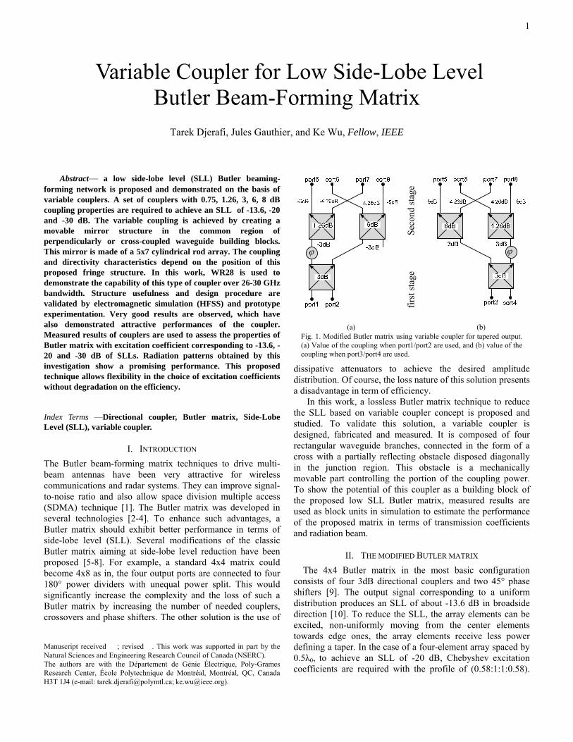
1
Abstract— a low side-lobe level (SLL) Butler beaming-
forming network is proposed and demonstrated on the basis of variable couplers. A set of couplers with 0.75, 1.26, 3, 6, 8 dB coupling properties are required to achieve an SLL of -13.6, -20 and -30 dB. The variable coupling is achieved by creating a movable mirror structure in the common region of perpendicularly or cross-coupled waveguide building blocks. This mirror is made of a 5x7 cylindrical rod array. The coupling and directivity characteristics depend on the position of this proposed fringe structure. In this work, WR28 is used to demonstrate the capability of this type of coupler over 26-30 GHz bandwidth. Structure usefulness and design procedure are validated by electromagnetic simulation (HFSS) and prototype experimentation. Very good results are observed, which have also demonstrated attractive performances of the coupler. Measured results of couplers are used to assess the properties of Butler matrix with excitation coefficient corresponding to -13.6, -20 and -30 dB of SLLs. Radiation patterns obtained by this investigation show a promising performance. This proposed technique allows flexibility in the choice of excitation coefficients without degradation on the efficiency. Index Terms —Directional coupler, Butler matrix, Side-Lobe Level (SLL), variable coupler.
I. INTRODUCTION
The Butler beam-forming matrix techniques to drive multi-beam antennas have been very attractive for wireless communications and radar systems. They can improve signal-to-noise ratio and also allow space division multiple access (SDMA) technique [1]. The Butler matrix was developed in several technologies [2-4]. To enhance such advantages, a Butler matrix should exhibit better performance in terms of side-lobe level (SLL). Several modifications of the classic Butler matrix aiming at side-lobe level reduction have been proposed [5-8]. For example, a standard 4x4 matrix could become 4x8 as in, the four output ports are connected to four 180° power dividers with unequal power split. This would significantly increase the complexity and the loss of such a Butler matrix by increasing the number of needed couplers, crossovers and phase shifters. The other solution is the use of
Manuscript received ; revised . This work was supported in part by the Natural Sciences and Engineering Research Council of Canada (NSERC). The authors are with the Département de Génie Électrique, Poly-Grames Research Center, École Polytechnique de Montréal, Montréal, QC, Canada H3T 1J4 (e-mail: [email protected]; [email protected]).
dissipative attenuators to achieve the desired amplitude distribution. Of course, the loss nature of this solution presents a disadvantage in term of efficiency.
In this work, a lossless Butler matrix technique to reduce the SLL based on variable coupler concept is proposed and studied. To validate this solution, a variable coupler is designed, fabricated and measured. It is composed of four rectangular waveguide branches, connected in the form of a cross with a partially reflecting obstacle disposed diagonally in the junction region. This obstacle is a mechanically movable part controlling the portion of the coupling power. To show the potential of this coupler as a building block of the proposed low SLL Butler matrix, measured results are used as block units in simulation to estimate the performance of the proposed matrix in terms of transmission coefficients and radiation beam.
II. THE MODIFIED BUTLER MATRIX
The 4x4 Butler matrix in the most basic configuration consists of four 3dB directional couplers and two 45° phase shifters [9]. The output signal corresponding to a uniform distribution produces an SLL of about -13.6 dB in broadside direction [10]. To reduce the SLL, the array elements can be excited, non-uniformly moving from the center elements towards edge ones, the array elements receive less power defining a taper. In the case of a four-element array spaced by 0.5λ0, to achieve an SLL of -20 dB, Chebyshev excitation coefficients are required with the profile of (0.58:1:1:0.58).
Variable Coupler for Low Side-Lobe Level Butler Beam-Forming Matrix
Tarek Djerafi, Jules Gauthier, and Ke Wu, Fellow, IEEE
Sec
ond
stag
e
firs
t sta
ge
(a) (b) Fig. 1. Modified Butler matrix using variable coupler for tapered output. (a) Value of the coupling when port1/port2 are used, and (b) value of the coupling when port3/port4 are used.
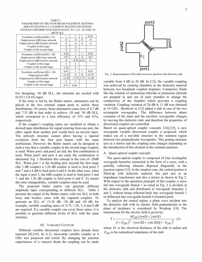
2
For designing -30 dB SLL, the elements are excited with (0.43:1:1:0.43) taper.
If the array is fed by the Butler matrix, attenuators can be placed in the two external output ports to realize these distributions. Of course, those attenuators cause loss of 4.7 dB and 7.33 dB in that order to achieve -20 and -30 dB SLL, which correspond to a loss efficiency of 33% and 41%, respectively.
If the coupler’s coupling ratios are modified to obtain a desired taper distribution for signal entering from one port, the other signal from another port would have an inverse taper. The network structure cannot allow having a tapered excitation from the four port beams with the same architecture. However, the Butler matrix can be designed in such a way that a variable coupler in the second stage couplers is used. When port1 and port2 are fed, the first combination is used. When port3 and port 4 are used, the combination is alternated. Fig .1 illustrates this concept in the case of -20dB SLL. When port 1 is the feeding port, beyond the first stage (the 3 dB coupler) a 1.26 dB coupler is used to feed ports 5 and 7 and a 6 dB to feed ports 6 and 8. In the other case, when the input is port 3, the 6dB coupler is used to feed ports 5 and 7, and the 1.26 dB coupler to feed ports 6 and 8. To ensure this inter-changeability, variable couplers must be used.
The proposed butler matrix can generate different amplitude taper corresponding to different SLL. Table I presents the output of the Butler matrix with low SLL in both lossy and lossless cases with the required couplers. To generate an SLL of -13.26 dB, -20 dB and -30 dB, for example, variable coupling ratios of: 0.75, 1.26, 3, 6 and 8 dB are required. If a variable coupler can cover these ratios, it is possible to generate different levels of SLL with the same structure.
III. VARIABLE COUPLER
Different variable directional couplers have already been reported [8]-[10]. In [11], microstrip variable coupler at 4 GHz was proposed and tested. By changing the junction capacitances of a varactor diode the coupling can be made
variable from 4 dB to 20 dB. In [12], the variable coupling was achieved by creating chambers in the dielectric material between two broadside coupled striplines. Conductive fluids like the solution of ammonium chloride or potassium chloride are pumped in and out of each chamber to change the conductivity of the chamber which provides a coupling variation. Coupling variation of 24 dB to 11 dB was obtained at 10 GHz. Brodwint in [13] added a slab in one of the two rectangular waveguides. The difference between phase constants of the main and the auxiliary waveguides changes by moving this dielectric slab, and therefore the properties of directional couplers are controlled. Based on quasi-optical coupler concepts [14]-[15], a new waveguide variable directional coupler is proposed, which makes use of a movable structure in the common region between two perpendicular waveguides. This grating structure acts as a mirror and the coupling ratio changes depending on the introduction of this element in the common junction.
A. Quasi-optical coupler concepts
The quasi-optical coupler is composed of four rectangular waveguide branches connected in the form of a cross, with a partially reflecting obstacle disposed diagonally in the junction region [15]. In the simplest case, the central portion is filled-up with dielectric material; this part acts as an impedance transformer and also a mirror as shown in Fig 2. With respect to the operation principle of this coupler, a wave fed into waveguide branch 1 as noted in Fig. 2 is divided, at the dielectric slab and distributed to waveguide branches 2 and 3, without being reflected back into waveguide branch 1 or diffracted into waveguide branch 4 (Isolated port).
To analyze the central region, a plane wave incident into the dielectric slab with its electric field perpendicular to the plane of incidence is considered by Wardrop [14]. The transmission for the electric field is given by:
2 2
4 cos sin
1 cos 2 sin 2 1
DN
DN DN
Z jT
Z j Z
(1)
where is the electrical thickness of the slab in radian and
DNZ is the normalized impedance of the slab:
TABLE I PARAMETERS OF THE FOUR-BEAM 4-ELEMENT ANTENNA
ARRAYS HAVING 0.5 λ ELEMENT SPACING EXCITED BY COURANT DISTRIBUTION EQUIVALENT TO -13.6, -20 AND -30
dB OF SLL
Excitation coefficient(SLL-13) Output power (dB) lossy network
Output power (dB) lossless network Coupler in first stage
Coupler in the second stage
1 1 1 0.58 -6 -6 -6 -6
-6 -6 -6 -6
3 -3 -3 -3
Excitation coefficient(SLL -20) Output power (dB) lossy network
Output power (dB) lossless network Coupler in first stage
Coupler in the second stage
0.58 1 1 0.58 -10.7 -6 -6 -10.7
-9 -4.26 -4.26 9 3 3
1.26 6
Excitation coefficient (SLL -30) Output power (dB)
Output power (dB) lossless network Coupler in first stage
Coupler in the second stage
0.43 1 1 0.43 -13.33 -6 -6 -13.33 -11.09 -3.75 -3.75 -11.09
3 3
0.75 8.06
port1
port3
1
2
Fig. 2. Representation of the ideal crossover junction with dielectric slab.
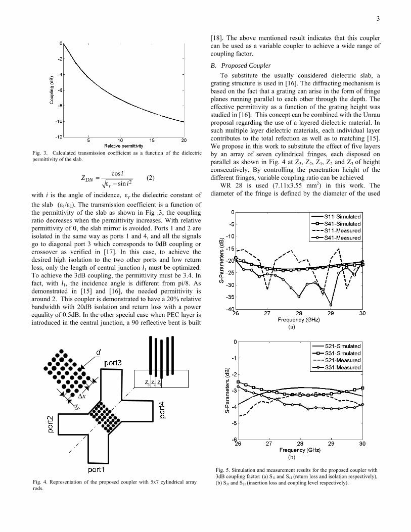
3
2
cos
sinDN
r
iZ
i
(2)
with i is the angle of incidence, r the dielectric constant of
the slab (ε1/ε2). The transmission coefficient is a function of the permittivity of the slab as shown in Fig .3, the coupling ratio decreases when the permittivity increases. With relative permittivity of 0, the slab mirror is avoided. Ports 1 and 2 are isolated in the same way as ports 1 and 4, and all the signals go to diagonal port 3 which corresponds to 0dB coupling or crossover as verified in [17]. In this case, to achieve the desired high isolation to the two other ports and low return loss, only the length of central junction l1 must be optimized. To achieve the 3dB coupling, the permittivity must be 3.4. In fact, with l1, the incidence angle is different from pi/8. As demonstrated in [15] and [16], the needed permittivity is around 2. This coupler is demonstrated to have a 20% relative bandwidth with 20dB isolation and return loss with a power equality of 0.5dB. In the other special case when PEC layer is introduced in the central junction, a 90 reflective bent is built
[18]. The above mentioned result indicates that this coupler can be used as a variable coupler to achieve a wide range of coupling factor.
B. Proposed Coupler
To substitute the usually considered dielectric slab, a grating structure is used in [16]. The diffracting mechanism is based on the fact that a grating can arise in the form of fringe planes running parallel to each other through the depth. The effective permittivity as a function of the grating height was studied in [16]. This concept can be combined with the Unrau proposal regarding the use of a layered dielectric material. In such multiple layer dielectric materials, each individual layer contributes to the total refection as well as to matching [15]. We propose in this work to substitute the effect of five layers by an array of seven cylindrical fringes, each disposed on parallel as shown in Fig. 4 at Z3, Z2, Z1, Z2 and Z3 of height consecutively. By controlling the penetration height of the different fringes, variable coupling ratio can be achieved
WR 28 is used (7.11x3.55 mm2) in this work. The diameter of the fringe is defined by the diameter of the used
Fig. 3. Calculated transmission coefficient as a function of the dielectricpermittivity of the slab.
(a)
(b)
Fig. 5. Simulation and measurement results for the proposed coupler with 3dB coupling factor: (a) S11
and S41
(return loss and isolation respectively),
(b) S31 and S21
(insertion loss and coupling level respectively).
xy
2z 1z3z
Fig. 4. Representation of the proposed coupler with 5x7 cylindrical array rods.
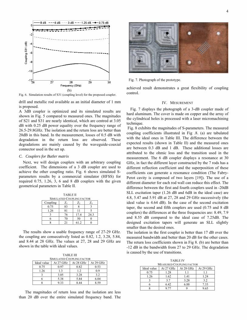
4
drill and metallic rod available as an initial diameter of 1 mm is proposed. A 3dB coupler is optimized and its simulated results are shown in Fig. 5 compared to measured ones. The magnitudes of S21 and S31 are nearly identical, which are centred at 3.05 dB with 0.25 dB power equality over the frequency range of 26.5-29.8GHz. The isolation and the return loss are better than 20dB in this band. In the measurement, losses of 0.5 dB with degradation in the return loss are observed. These degradations are mainly caused by the waveguide-coaxial connector used in the set up.
C. Couplers for Butler matrix
Next, we will design couplers with an arbitrary coupling coefficient. The dimensions of a 3 dB coupler are used to achieve the other coupling ratio. Fig. 6 shows simulated S-parameters results by a commercial simulator (HFSS) for required 0.75, 1.26, 3, 6 and 8 dB couplers with the given geometrical parameters in Table II.
TABLE II
SIMULATED COUPLING FACTOR Coupling Z1 Z2 Z3
0.75 83 8 3 1.26 81 11 5
3 76 17.4 24.3 6 70 50 0 8 21 61.2 0
The results show a usable frequency range of 27-29 GHz.
the coupling are consecutively listed as 0.82, 1.2, 3.28, 5.84, and 8.44 at 28 GHz. The values at 27, 28 and 29 GHz are shown in the table with ideal values.
TABLE III
SIMULATED COUPLING FACTOR Ideal value At 27 GHz At 28 GHz At 29 GHz
0.75 0.97 0.82 0.53 1.26 1.3 1.2 0.9
3 3.05 3.28 3.2 6 5.38 5.84 6.04 8 9.33 8.44 8.59
The magnitudes of return loss and the isolation are less
than 20 dB over the entire simulated frequency band. The
achieved result demonstrates a great flexibility of coupling control.
IV. MESUREMENT
Fig. 7 displays the photograph of a 3-dB coupler made of hard aluminum. The cover is made on copper and the array of the cylindrical holes is processed with a laser micromachining technique. Fig. 8 exhibits the magnitudes of S-parameters. The measured coupling coefficients illustrated in Fig .8. (a) are tabulated with the ideal ones in Table III. The difference between the expected results (shown in Table II) and the measured ones are between 0.3 dB and 1 dB. These additional losses are attributed to the ohmic loss and the transition used in the measurement. The 6 dB coupler displays a resonance at 30 GHz, in fact the different layer constructed by the 7 rods has a different reflection coefficient and the superposition of these coefficients can generate a resonance condition (The Fabry-Perot cavity is composed of two layers [19]). The use of a different diameter for each rod wall can reduce this effect. The difference between the first and fourth couplers used in -20dB SLL excitation taper (1.26 dB and 6dB in the ideal case) are 4.8, 5.47 and 5.91 dB at 27, 28 and 29 GHz successively (the ideal value is 4.64 dB). In the case of the second excitation taper, the second and fifth couplers are used (0.75 and 8 dB couplers) the differences at the three frequencies are: 8.49, 7.9 and 8.55 dB compared to the ideal case of 7.25dB. The designed excitation tapers will generate an SLL slightly smaller than the desired ones. The isolation in the first coupler is better than 17 dB over the measured bandwidth and better than 20 dB for the other cases. The return loss coefficients shown in Fig 8. (b) are better than -12 dB in the bandwidth from 27 to 29 GHz. The degradation is caused by the use of transitions.
TABLE IV
MEASURED COUPLING FACTOR Ideal value At 27 GHz At 28 GHz At 29 GHz
0.75 1.28 1.1 1.1 1.26 1.62 1.41 1.24
3 3.7 3.28 3.2 6 6.42 6.88 7.33 8 9.77 9 9.65
(b) Fig. 6. Simulation results of S31 (coupling level) for the proposed coupler.
Fig. 7. Photograph of the prototype.
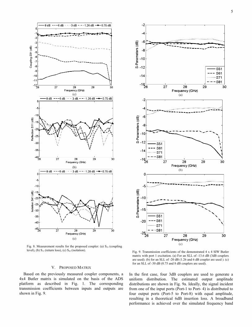
5
V. PROPOSED MATRIX
Based on the previously measured coupler components, a 4x4 Butler matrix is simulated on the basis of the ADS platform as described in Fig. 1. The corresponding transmission coefficients between inputs and outputs are shown in Fig. 9.
In the first case, four 3dB couplers are used to generate a uniform distribution. The estimated output amplitude distributions are shown in Fig. 9a. Ideally, the signal incident from one of the input ports (Port-1 to Port- 4) is distributed to four output ports (Port-5 to Port-8) with equal amplitude, resulting in a theoretical 6dB insertion loss. A broadband performance is achieved over the simulated frequency band
(a)
(b)
(c)
Fig. 9. Transmission coefficients of the demonstrated 4 x 4 SIW Butler matrix with port 1 excitation. (a) For an SLL of -13.6 dB (3dB couplers are used). (b) for an SLL of -20 dB (1.26 and 6 dB coupler are used ). (c) for an SLL of -30 dB (0.75 and 8 dB couplers are used).
(c)
(b)
(c)
Fig. 8. Measurement results for the proposed coupler: (a) S21
(coupling
level), (b) S11 (return loss), (c) S41
(isolation).
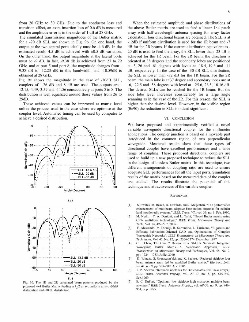
6
from 26 GHz to 30 GHz. Due to the conductor loss and transition effect, an extra insertion loss of 0.6 dB is measured and the amplitude error is in the order of 1 dB at 28 GHz. The simulated transmission magnitudes of the Butler matrix for a -20 dB SLL are shown in Fig. 9b. On one hand, the output at the two central ports ideally must be -4.6 dB. In the estimated result, 4.5 dB is achieved with ±0.5 dB variation. On the other hand, the output magnitude at the lateral ports must be -9 dB. In fact, -9.38 dB is achieved from 27 to 29 GHz. and at port 5 and port 8, the magnitude changes from -9.38 dB to -12.23 dB in this bandwidth, and -10.59dB is obtained at 28 GHz. Fig. 9c shows the magnitude in the case of -30dB SLL, couplers of 1.26 dB and 8 dB are used. The outputs are -12.15,-4.49,-3.59 and -11.56 consecutively at ports 5 to 8. The distribution is well equalized around those values from 26 to 29dB.
These achieved values can be improved at matrix level unlike the process used in the case where we optimise at the coupler level. Automated tuning can be used by computer to achieve a desired distribution.
When the estimated amplitude and phase distributions of the above Butler matrix are used to feed a linear 1×4 patch
array with half-wavelength antenna spacing for array factor calculation, four directional beams are obtained. The SLL is at -12dB if uniform distribution is used for the 1R beam and -7 dB for the 2R beams. If the current distribution equivalent to -20 dB is used to feed the array, the SLL lower than -23 dB is achieved for the 1R beam. For the 2R beam, the direction is oriented at 38 degrees and the secondary lobes are positioned at -3,-26 and -61 degrees with levels at -18.4,-19.6 and -11 dB, respectively. In the case of the -30 dB SLL distribution, the SLL is lower than -32 dB for the 1R beam. For the 2R beam the main lobe is at 37 degree and secondary lobes are at -6, -22.5 and -58 degrees with level at -25.6,-26.5,-10.16 dB. The desired SLLs can be reached for the 1R beam. But the side lobe level increases considerably for a large angle scanning as in the case of the 2R. For this reason, the SLL is higher than the desired level. However, in the visible region (θ±90) the reduction in SLL is indeed significant.
VI. CONCLUSION
We have proposed and experimentally verified a novel variable waveguide directional coupler for the millimeter applications. The coupler junction is based on a movable part introduced in the common region of two perpendicular waveguide. Measured results show that these types of directional coupler have excellent performances and a wide range of coupling. These proposed directional couplers are used to build up a new proposed technique to reduce the SLL in the design of lossless Butler matrix. In this technique, two different arrangements of coupling ratio are used to ensure adequate SLL performances for all the input ports. Simulation results of the matrix based on the measured data of the coupler are studied. The results illustrate the potential of this technique and attractiveness of the variable coupler.
REFERENCES
[1] S. Swales, M. Beach, D. Edwards, and J. Mcgeehan, “The performance
enhancement of multibeam adaptive base-station antennas for cellular land mobile radio systems.” IEEE. Trans. VT., vol. 39, no. 1, Feb. 1990.
[2] M. Nedil, , T. A. Denidni, and L. Talbi, “Novel Butler matrix using CPW multilayer technology,” IEEE Trans. Microwave Theory and Tech., Vol. 54, 499–507, 2006.
[3] F. Alessandri, M. Dionigi, R. Sorrentino, L. Tarricone, “Rigorous and Efficient Fabrication-Oriented CAD and Optimization of Complex Waveguide Networks”, IEEE Transactions on Microwave Theory and Techniques, Vol. 45, No. 12, pp.: 2366-2374, December 1997
[4] C.J. Chen, T.H. Chu, “ Design of a 60-GHz Substrate Integrated Waveguide Butler Matrix—A Systematic Approach,” IEEE Transactions on Microwave Theory and Techniques, Vol. 58, No. 7, pp.: 1724 - 1733, Juillet 2010
[5] K. Wincza, S. Gruszczyn´ski, and K. Sachse, “Reduced sidelobe four beam antenna array fed by modified Butler matrix,” Electron. Lett., vol.42, no. 9, pp. 508–509, Apr. 2006.
[6] J. P. Shelton, “Reduced sidelobes for Butler-matrix-fed linear arrays,” IEEE Trans. Antennas Propag., vol. AP-17, no. 5, pp. 645–647, Sep.1969.
[7] E. C. DuFort, “Optimum low sidelobe high crossover multiple beam antennas,” IEEE Trans. Antennas Propag., vol. AP-33, no. 9, pp. 946–954, Sep. 1985.
(a)
(b) Fig. 10. The 1R and 2R calculated beam patterns produced by the proposed 4x4 Butler Matrix feeding a λ
o/2 array, uniform array, -20dB
distribution and -30 dB distribution.
7
[8] S. Gruszczynski, K. Wincza, and K. Sachse, “Reduced sidelobe fourbeamN-element antenna arrays fed by 4x4 Butler matrices,” IEEE Antennas Wireless Propag. Lett., vol. 5, no. 1, pp. 430–434, Dec. 2006.
[9] J. Butler and R. Lowe, “Beam-forming matrix simplifies design of electrically scanned antennas, ” Electronic Design, no. 9, pp. 170-173, April 1961.
[10] W.L. Stutzman, Antenna Theory and Design, 2nd Edition. [11] S. Toyoda, “Variable Coupling Directional Couplers Using Varactor
Diodes, ” Microwave Symposium Digest, MTT-S International, 1982. Pp.
[12] S. Niyogi, J. Scott, and K. Ghorbani, “Variable Directional Coupler Employing Microfluidics,” 38th EuropeanMicrowave Conference, 2008, pp. 207 – 210.
[13] M. E. Brodwint, and V. Ramaswamy, “Continuously Variable Directional Couplers in Rectangular Waveguide, ” IEEE Transactions on Microwave Theory and Techniques, vol. 11, issue 2, pp. 137-142.Mar. 1963.
[14] B. Wardrop, “A quasi-optical directinal coupler,” Marconi Rev., vol. 35, no. 185, pp. 159–168, 1972.
[15] U. Unrau, “Waveguide Directional Coupler,” U.S. Patent 4 034 315, Jul. 5, 1977.
[16] T. Djerafi, J. Gauthier, K. Wu, “Quasi-Optical Cruciform Substrate Integrated Waveguide (SIW) Coupler for Millimeter-Wave Systems,” IMS2010, Anaheim, pp 716-719.
[17] T. Djerafi, and K. Wu, “A 60 GHz Substrate Integrated Waveguide Crossover structure,” EUMC 2009, pp1014-1017, Rome 2009.
[18] P. K. Park, R. L. Eisenhart, S. E. Bradshaw, “Matched, Dual Mode Square Waveguide Corner,” International Microwave Symposium Digest, 1986 MTT-S pp 155 – 156, Baltimore, MD, USA.
[19] H. Boutayeb, T.A. Denidni, AR. Sebak, L. Talbi, “ Band Structure Analysis of Crystals with Discontinuous Metallic Wires,” IEEE Microwave and Wireless Components Letters, vol. 15, no7, pp. 484-486. 2005.
[20] V. Miraftab, R.R. Mansour, “Fully Automated RF/Microwave Filter Tuning by Extracting Human Experience Using Fuzzy” IEEE Transactions on Controllers, Circuits and Systems. Pp. 1357 - 1367, vol: 55 Issue: 5, June 2008.

108
ARTICLE VII: 77 GHZ RECOMBINANT SUBSTRATE INTEGRATED
WAVEGUIDE POWER DIVIDER
Tarek Djerafi, Andreas Patrovsky, Member, IEEE, and Ke Wu, Fellow, IEEE
Article soumis avril 2011 IEEE Letters on antenna and propagation.
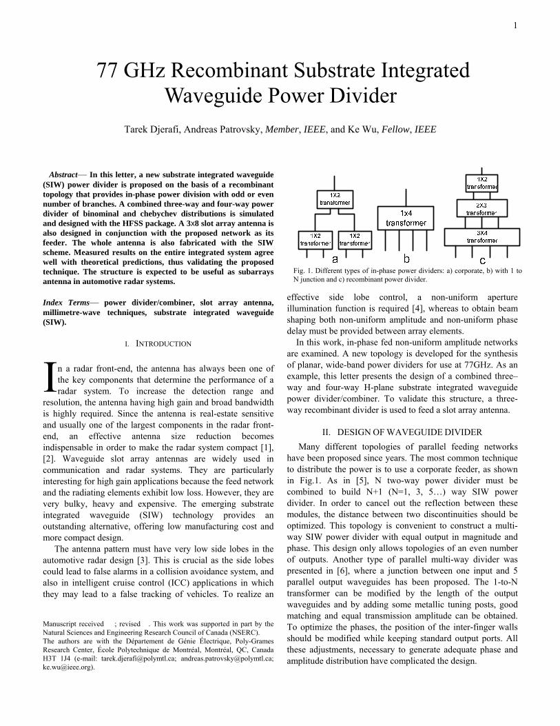
1
Abstract— In this letter, a new substrate integrated waveguide (SIW) power divider is proposed on the basis of a recombinant topology that provides in-phase power division with odd or even number of branches. A combined three-way and four-way power divider of binominal and chebychev distributions is simulated and designed with the HFSS package. A 3x8 slot array antenna is also designed in conjunction with the proposed network as its feeder. The whole antenna is also fabricated with the SIW scheme. Measured results on the entire integrated system agree well with theoretical predictions, thus validating the proposed technique. The structure is expected to be useful as subarrays antenna in automotive radar systems.
Index Terms— power divider/combiner, slot array antenna, millimetre-wave techniques, substrate integrated waveguide (SIW).
I. INTRODUCTION
n a radar front-end, the antenna has always been one of the key components that determine the performance of a radar system. To increase the detection range and
resolution, the antenna having high gain and broad bandwidth is highly required. Since the antenna is real-estate sensitive and usually one of the largest components in the radar front-end, an effective antenna size reduction becomes indispensable in order to make the radar system compact [1], [2]. Waveguide slot array antennas are widely used in communication and radar systems. They are particularly interesting for high gain applications because the feed network and the radiating elements exhibit low loss. However, they are very bulky, heavy and expensive. The emerging substrate integrated waveguide (SIW) technology provides an outstanding alternative, offering low manufacturing cost and more compact design.
The antenna pattern must have very low side lobes in the automotive radar design [3]. This is crucial as the side lobes could lead to false alarms in a collision avoidance system, and also in intelligent cruise control (ICC) applications in which they may lead to a false tracking of vehicles. To realize an
Manuscript received ; revised . This work was supported in part by the Natural Sciences and Engineering Research Council of Canada (NSERC). The authors are with the Département de Génie Électrique, Poly-Grames Research Center, École Polytechnique de Montréal, Montréal, QC, Canada H3T 1J4 (e-mail: [email protected]; [email protected]; [email protected]).
effective side lobe control, a non-uniform aperture illumination function is required [4], whereas to obtain beam shaping both non-uniform amplitude and non-uniform phase delay must be provided between array elements.
In this work, in-phase fed non-uniform amplitude networks are examined. A new topology is developed for the synthesis of planar, wide-band power dividers for use at 77GHz. As an example, this letter presents the design of a combined three–way and four-way H-plane substrate integrated waveguide power divider/combiner. To validate this structure, a three-way recombinant divider is used to feed a slot array antenna.
II. DESIGN OF WAVEGUIDE DIVIDER
Many different topologies of parallel feeding networks have been proposed since years. The most common technique to distribute the power is to use a corporate feeder, as shown in Fig.1. As in [5], N two-way power divider must be combined to build N+1 (N=1, 3, 5…) way SIW power divider. In order to cancel out the reflection between these modules, the distance between two discontinuities should be optimized. This topology is convenient to construct a multi-way SIW power divider with equal output in magnitude and phase. This design only allows topologies of an even number of outputs. Another type of parallel multi-way divider was presented in [6], where a junction between one input and 5 parallel output waveguides has been proposed. The 1-to-N transformer can be modified by the length of the output waveguides and by adding some metallic tuning posts, good matching and equal transmission amplitude can be obtained. To optimize the phases, the position of the inter-finger walls should be modified while keeping standard output ports. All these adjustments, necessary to generate adequate phase and amplitude distribution have complicated the design.
77 GHz Recombinant Substrate Integrated Waveguide Power Divider
Tarek Djerafi, Andreas Patrovsky, Member, IEEE, and Ke Wu, Fellow, IEEE
I
Fig. 1. Different types of in-phase power dividers: a) corporate, b) with 1 to N junction and c) recombinant power divider.
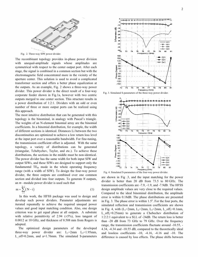
2
The recombinant topology provides in-phase power division with unequal-amplitude signals whose amplitudes are symmetrical with respect to the center output port. After each stage, the signal is combined in a common section but with the electromagnetic field concentrated more in the vicinity of the aperture center. This solution is used to avoid a complicated transformer section and offers a better phase equalization at the outputs. As an example, Fig. 2 shows a three-way power divider. This power divider is the direct result of a four-way corporate feeder shown in Fig.1a, however with two centric outputs merged to one center section. This structure results in a power distribution of 1:2:1. Dividers with an odd or even number of three or more output ports can be realized using this approach. The most intuitive distribution that can be generated with this topology is the binominal, in analogy with Pascal’s triangle. The weights of an N-element binomial array are the binomial coefficients. In a binomial distribution, for example, the width of different sections is identical. Distances Li between the two discontinuities are optimized to achieve a low return loss level at the input port over a reasonable bandwidth. For fine-tuning, the transmission coefficient offset is adjusted. With the same topology, a variety of distributions can be generated (triangular, Tchebychev, Taylor, and etc.). To achieve these distributions, the sections in the middle must be non-identical. The power divider has the same width for both input SIW and output SIWs, and these SIWs are designed to support only the fundamental TEl0 mode in the whole operating frequency range (with a width of SIW). To design the four-way power divider, the three outputs are combined over one common section and divided into four outputs. To generate N outputs, an m –module power divider is used such that
N 1
i 1
m N i
(1)
In this work, the HFSS package was used to design and develop such power dividers. Parameter adjustments are iterated repeatedly to achieve the required unequal power values and good input matching condition. Also, one design criterion was to get equal phase at all outputs. A substrate with relative permittivity of 2.94 (±5%), loss tangent of 0.0012 at 10 GHz, and thickness of 0.508 mm from Rogers is adopted.
The optimized design parameters of the developed three-way power divider are: L1=2mm L2=1.95mm, L_off=0.2mm, and a=1.76mm. The simulated S-parameters
are shown in Fig .3, and the input matching for the power divider is better than 20 dB from 73.5 to 80 GHz. The transmission coefficients are -7.9, -1.9, and -7.9dB. The HFSS design amplitude values are very close to the required values. Compared to the ideal binominal distribution, the amplitude error is within 0.18dB. The phase distributions are presented in Fig. 3. The phase error is within 1.5o. For the four ports, the simulated reflection and transmission coefficients are shown in Fig. 4, with (L1=2mm, L2=2mm, L3=2mm, L_off1=0.1mm, L_off2=0.25mm) to generate a Chebechev distribution of 1:2:2:1 equivalent to a SLL of -24dB. The return loss is better than -20 dB from 73 GHz to 79 GHz. Over the frequency range, the transmission coefficients fluctuate around -10.55, -4.34, -4.34 and -10.55 dB, compared to the theoretically ideal and lossless coefficients -10, -4.16, -4.16 and -10. The difference is caused by loss effects. The phase shifts between
Fig. 2. Three-way SIW power divider.
Fig. 4. Simulated S-parameters of the four-way power divider.
Fig. 3. Simulated S-parameters of the three-way power divider.
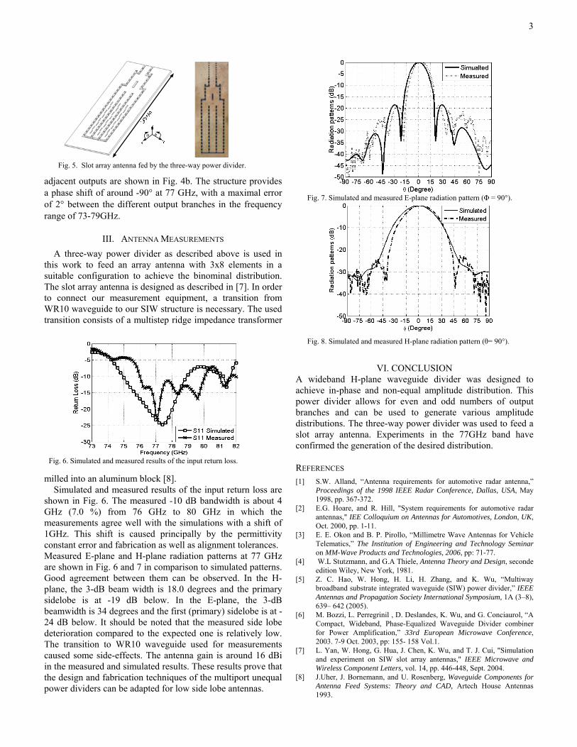
3
adjacent outputs are shown in Fig. 4b. The structure provides a phase shift of around -90° at 77 GHz, with a maximal error of 2° between the different output branches in the frequency range of 73-79GHz.
III. ANTENNA MEASUREMENTS
A three-way power divider as described above is used in this work to feed an array antenna with 3x8 elements in a suitable configuration to achieve the binominal distribution. The slot array antenna is designed as described in [7]. In order to connect our measurement equipment, a transition from WR10 waveguide to our SIW structure is necessary. The used transition consists of a multistep ridge impedance transformer
milled into an aluminum block [8]. Simulated and measured results of the input return loss are
shown in Fig. 6. The measured -10 dB bandwidth is about 4 GHz (7.0 %) from 76 GHz to 80 GHz in which the measurements agree well with the simulations with a shift of 1GHz. This shift is caused principally by the permittivity constant error and fabrication as well as alignment tolerances. Measured E-plane and H-plane radiation patterns at 77 GHz are shown in Fig. 6 and 7 in comparison to simulated patterns. Good agreement between them can be observed. In the H-plane, the 3-dB beam width is 18.0 degrees and the primary sidelobe is at -19 dB below. In the E-plane, the 3-dB beamwidth is 34 degrees and the first (primary) sidelobe is at -24 dB below. It should be noted that the measured side lobe deterioration compared to the expected one is relatively low. The transition to WR10 waveguide used for measurements caused some side-effects. The antenna gain is around 16 dBi in the measured and simulated results. These results prove that the design and fabrication techniques of the multiport unequal power dividers can be adapted for low side lobe antennas.
VI. CONCLUSION
A wideband H-plane waveguide divider was designed to achieve in-phase and non-equal amplitude distribution. This power divider allows for even and odd numbers of output branches and can be used to generate various amplitude distributions. The three-way power divider was used to feed a slot array antenna. Experiments in the 77GHz band have confirmed the generation of the desired distribution.
REFERENCES [1] S.W. Alland, “Antenna requirements for automotive radar antenna,”
Proceedings of the 1998 IEEE Radar Conference, Dallas, USA, May 1998, pp. 367-372.
[2] E.G. Hoare, and R. Hill, "System requirements for automotive radar antennas," IEE Colloquium on Antennas for Automotives, London, UK, Oct. 2000, pp. 1-11.
[3] E. E. Okon and B. P. Pirollo, “Millimetre Wave Antennas for Vehicle Telematics,” The Institution of Engineering and Technology Seminar on MM-Wave Products and Technologies, 2006, pp: 71-77.
[4] W.L Stutzmann, and G.A Thiele, Antenna Theory and Design, seconde edition Wiley, New York, 1981.
[5] Z. C. Hao, W. Hong, H. Li, H. Zhang, and K. Wu, “Multiway broadband substrate integrated waveguide (SIW) power divider,” IEEE Antennas and Propagation Society International Symposium, 1A (3–8), 639– 642 (2005).
[6] M. Bozzi, L. Perregrinil , D. Deslandes, K. Wu, and G. Conciaurol, “A Compact, Wideband, Phase-Equalized Waveguide Divider combiner for Power Amplification,” 33rd European Microwave Conference, 2003. 7-9 Oct. 2003, pp: 155- 158 Vol.1.
[7] L. Yan, W. Hong, G. Hua, J. Chen, K. Wu, and T. J. Cui, "Simulation and experiment on SIW slot array antennas," IEEE Microwave and Wireless Component Letters, vol. 14, pp. 446-448, Sept. 2004.
[8] J.Uher, J. Bornemann, and U. Rosenberg, Waveguide Components for Antenna Feed Systems: Theory and CAD, Artech House Antennas 1993.
Fig. 6. Simulated and measured results of the input return loss.
Fig. 5. Slot array antenna fed by the three-way power divider.
Fig. 7. Simulated and measured E-plane radiation pattern (Φ = 90°).
Fig. 8. Simulated and measured H-plane radiation pattern (θ= 90°).
112
ARTICLE VIII: CORRUGATED SUBSTRATE INTEGRATED
WAVEGUIDE (SIW) ANTIPODAL LINEARLY TAPERED SLOT ANTENNA
ARRAY FEED BY QUASI-TRIANGULAR POWER DIVIDER
Tarek Djerafi, and Ke Wu
Article revisé avril 2011 IEEE Transactions on Microwave Theory and Techniques.
1
Abstract— In this paper, a new configuration of Tapered Slot
Antenna (TSA) with improved radiation pattern is proposed and studied. This antenna is designed in the form of a substrate integrated waveguide (SIW) array with respect to side lobe level constraints. For side lobe reduction, a simple quasi-triangular distribution is proposed and is accomplished uniquely by means of 3dB power dividers. A 12-way series feed network with T-junction is designed and demonstrated. Radiation features of the antenna array are discussed to illustrate the accomplishment of a low side lobe level (-19dB) of the array. The proposed antenna demonstrates the ability of the SIW technology to achieve a very low side lobe in a simple, compact and planar structure.
Index Terms— power divider/combiner, series feed, sidelobe level (SLL), substrate integrated waveguide (SIW), tapered slot array (TSA).
I. INTRODUCTION
n many practical system applications, such as microwave and millimeter-wave radar, communication and imaging, it
is necessary to accommodate antenna in those systems design and implementation with high gain, low side lobe level (SLL) and low cross-polarisation [1]-[2]. Such attractive characteristics can ensure low interference, high resolution and long range performances. This is crucial in meeting system specification. Inappropriate side lobes lead to false alarm in the use of a collision avoidance radar system for intelligent cruise control (ICC) applications. In this case, the SLL problem can lead to a dangerous situation in the tracking of vehicles [3].
To meet the preset gain requirement, simple antenna element is generally not sufficient. An appropriate antenna array must be used. In the design of such an array, not only antenna element is important, but also feeding structure presents a critical factor for achieving a specific performance. The element-to-element spacing defines the state of grating lobes while influencing the desired high gain and scan angle [4][5]. Of course, this spacing must be less than λo (free space wavelength). In other words, the width of elements has to be
Manuscript received ; revised . This work was supported in part by the Natural Sciences and Engineering Research Council of Canada (NSERC). The authors are with the Département de Génie Électrique, Poly-Grames Research Center, École Polytechnique de Montréal, Montréal, QC, Canada H3T 1J4 (e-mail: [email protected]; [email protected]).
narrower than λo. Another source that deteriorates the SLL dramatically is
related to any extra-components placed on the same substrate that cause spurious radiation in broadside. These spurious radiations have less effect on the end-fire antenna [1], such as tapered slot antenna (TSA) [6]. Several TSA designs have been reported [5-15]., namely: LTSA (Linearly Tapered Slot Antenna), Vivaldi (Exponentially Tapered Slot Antenna), CWSA (Constant Width Slot Antenna) and BLTSA (Broken Linearly Tapered Slot Antenna) . It is well-known that the TSA features high gain, low VSWR, and wide bandwidth. However, antenna width reduction is necessary when it is used to form an antenna array. It has been documented that a reduced antipodal LTSA (ALTSA) antenna width is closely associated with degradation in radiation pattern, resulting in a significant problem for the design of compact TSAs [9].
Recent emerging research and development suggest that the substrate integrated waveguide (SIW) technology possesses attractive features, such as low-profile, low-weight, low-cost, easy implementation compatible with current microwave and millimetre-wave design and fabrication platforms. So far, a vast range of SIW components[12-21], including filters, phase shifters, transitions, couplers, power dividers, and diplexers have been proposed and studied]. This scheme has been demonstrated for its nascent applications to a wide range of antennas and feeding networks as well as beam-forming architectures [12-16]. The radiation-lossless quality of the SIW structure presents an excellent potential to design array antenna feeds. In fact, the inherent radiation loss and/or cross-talk in microstrip technology used as array feeder greatly
Corrugated Substrate Integrated Waveguide (SIW) Antipodal Linearly Tapered Slot Antenna Array Fed by Quasi-Triangular Power Divider
Tarek Djerafi, and Ke Wu, Fellow, IEEE
I
Fig. 1. Corrugated antipodal Linearly Tapered Slot Array (LTSA) fed by SIW structure and microstrip to SIW transition.
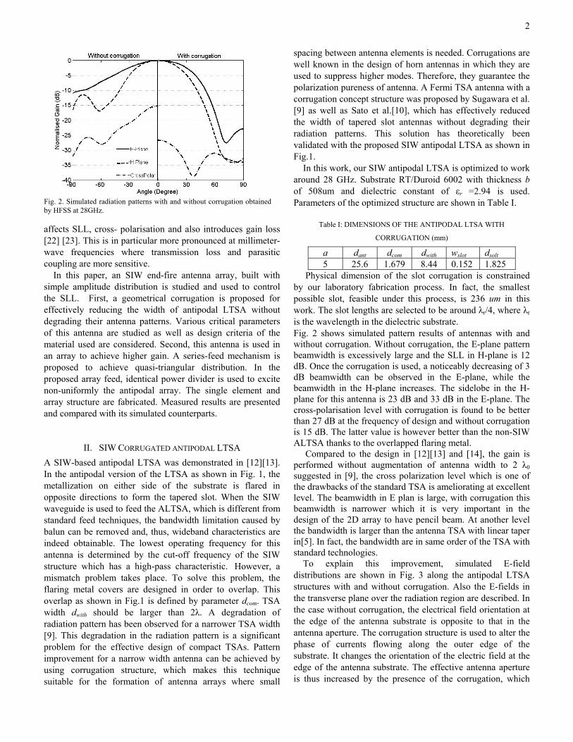
2
affects SLL, cross- polarisation and also introduces gain loss [22] [23]. This is in particular more pronounced at millimeter-wave frequencies where transmission loss and parasitic coupling are more sensitive.
In this paper, an SIW end-fire antenna array, built with simple amplitude distribution is studied and used to control the SLL. First, a geometrical corrugation is proposed for effectively reducing the width of antipodal LTSA without degrading their antenna patterns. Various critical parameters of this antenna are studied as well as design criteria of the material used are considered. Second, this antenna is used in an array to achieve higher gain. A series-feed mechanism is proposed to achieve quasi-triangular distribution. In the proposed array feed, identical power divider is used to excite non-uniformly the antipodal array. The single element and array structure are fabricated. Measured results are presented and compared with its simulated counterparts.
II. SIW CORRUGATED ANTIPODAL LTSA
A SIW-based antipodal LTSA was demonstrated in [12][13]. In the antipodal version of the LTSA as shown in Fig. 1, the metallization on either side of the substrate is flared in opposite directions to form the tapered slot. When the SIW waveguide is used to feed the ALTSA, which is different from standard feed techniques, the bandwidth limitation caused by balun can be removed and, thus, wideband characteristics are indeed obtainable. The lowest operating frequency for this antenna is determined by the cut-off frequency of the SIW structure which has a high-pass characteristic. However, a mismatch problem takes place. To solve this problem, the flaring metal covers are designed in order to overlap. This overlap as shown in Fig.1 is defined by parameter dcom. TSA width dwith should be larger than 2λ. A degradation of radiation pattern has been observed for a narrower TSA width [9]. This degradation in the radiation pattern is a significant problem for the effective design of compact TSAs. Pattern improvement for a narrow width antenna can be achieved by using corrugation structure, which makes this technique suitable for the formation of antenna arrays where small
spacing between antenna elements is needed. Corrugations are well known in the design of horn antennas in which they are used to suppress higher modes. Therefore, they guarantee the polarization pureness of antenna. A Fermi TSA antenna with a corrugation concept structure was proposed by Sugawara et al. [9] as well as Sato et al.[10], which has effectively reduced the width of tapered slot antennas without degrading their radiation patterns. This solution has theoretically been validated with the proposed SIW antipodal LTSA as shown in Fig.1.
In this work, our SIW antipodal LTSA is optimized to work around 28 GHz. Substrate RT/Duroid 6002 with thickness b of 508um and dielectric constant of εr =2.94 is used. Parameters of the optimized structure are shown in Table I.
Table I: DIMENSIONS OF THE ANTIPODAL LTSA WITH
CORRUGATION (mm)
a dant dcom dwith wslot dsolt 5 25.6 1.679 8.44 0.152 1.825
Physical dimension of the slot corrugation is constrained by our laboratory fabrication process. In fact, the smallest possible slot, feasible under this process, is 236 um in this work. The slot lengths are selected to be around λr/4, where λr is the wavelength in the dielectric substrate. Fig. 2 shows simulated pattern results of antennas with and without corrugation. Without corrugation, the E-plane pattern beamwidth is excessively large and the SLL in H-plane is 12 dB. Once the corrugation is used, a noticeably decreasing of 3 dB beamwidth can be observed in the E-plane, while the beamwidth in the H-plane increases. The sidelobe in the H-plane for this antenna is 23 dB and 33 dB in the E-plane. The cross-polarisation level with corrugation is found to be better than 27 dB at the frequency of design and without corrugation is 15 dB. The latter value is however better than the non-SIW ALTSA thanks to the overlapped flaring metal.
Compared to the design in [12][13] and [14], the gain is performed without augmentation of antenna width to 2 λ0 suggested in [9], the cross polarization level which is one of the drawbacks of the standard TSA is ameliorating at excellent level. The beamwidth in E plan is large, with corrugation this beamwidth is narrower which it is very important in the design of the 2D array to have pencil beam. At another level the bandwidth is larger than the antenna TSA with linear taper in[5]. In fact, the bandwidth are in same order of the TSA with standard technologies.
To explain this improvement, simulated E-field distributions are shown in Fig. 3 along the antipodal LTSA structures with and without corrugation. Also the E-fields in the transverse plane over the radiation region are described. In the case without corrugation, the electrical field orientation at the edge of the antenna substrate is opposite to that in the antenna aperture. The corrugation structure is used to alter the phase of currents flowing along the outer edge of the substrate. It changes the orientation of the electric field at the edge of the antenna substrate. The effective antenna aperture is thus increased by the presence of the corrugation, which
Fig. 2. Simulated radiation patterns with and without corrugation obtained by HFSS at 28GHz.
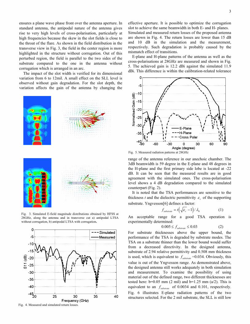
3
ensures a plane wave phase front over the antenna aperture. In standard antenna, the antipodal nature of the antenna gives rise to very high levels of cross-polarisation, particularly at high frequencies because the skew in the slot fields is close to the throat of the flare. As shown in the field distribution in the transverse view in Fig. 3, the field in the center region is more highlighted in the structure without corrugation. Out of this perturbed region, the field is parallel to the two sides of the substrate compared to the one in the antenna without corrugation which is arranged in an arc.
The impact of the slot width is verified for its dimensional variation from 6 to 12mil. A small effect on the SLL level is observed without gain degradation. For the slot depth, the variation affects the gain of the antenna by changing the
effective aperture. It is possible to optimize the corrugation slot to achieve the same beamwidth in both E- and H- planes. Simulated and measured return losses of the proposed antenna are shown in Fig. 4. The return losses are lower than 15 dB and 10 dB in the simulation and the measurement, respectively. Such degradation is probably caused by the mismatch effect of transitions.
E-plane and H-plane patterns of the antenna as well as the cross-polarisations at 28GHz are measured and shown in Fig. 5. The achieved gain is 12.2 dBi against the simulated 11.9 dBi. This difference is within the calibration-related tolerance
range of the antenna reference in our anechoic chamber. The 3dB beamwidth is 59 degree in the E-plane and 48 degrees in the H-plane and the first primary side lobe is located at -22 dB. It can be seen that the measured results are in good agreement with the simulated ones. The cross-polarisation level shows a 4 dB degradation compared to the simulated counterpart (Fig. 2).
It is noted that the TSA performances are sensitive to the thickness t and the dielectric permittivity r of the supporting
substrate. Yngvesson[6] defines a factor:
01 /substrate rf t (1)
An acceptable range for a good TSA operation is experimentally determined:
0.005 0.03substratef (2)
For substrate thicknesses above the upper bound, the performance of the TSA is degraded by substrate modes. The TSA on a substrate thinner than the lower bound would suffer from a decreased directivity. In the designed antenna, substrate of 2.94 relative permittivity and 0.508 mm thickness is used, which is equivalent to substratef =0.034. Obviously, this
value is out of the Yngvesson range. As demonstrated above, the designed antenna still works adequately in both simulation and measurement. To examine the possibility of using material out of the defined range, two different thicknesses are tested here: b=0.05 mm (2 mil) and b=1.25 mm (a/2). This is equivalent to an substratef of 0.0034 and 0.101, respectively.
Fig. 6 illustrates E-plane radiation patterns of the two structures selected. For the 2 mil substrate, the SLL is still low
Fig. 5. Measured radiation patterns at 28GHz
Fig. 3. Simulated E-field magnitude distributions obtained by HFSS at 28GHz, along the antenna and in transverse cut a) antipodal LTSA without corrugation, b) antipodal LTSA with corrugation.
Fig. 4. Measured and simulated return losses.
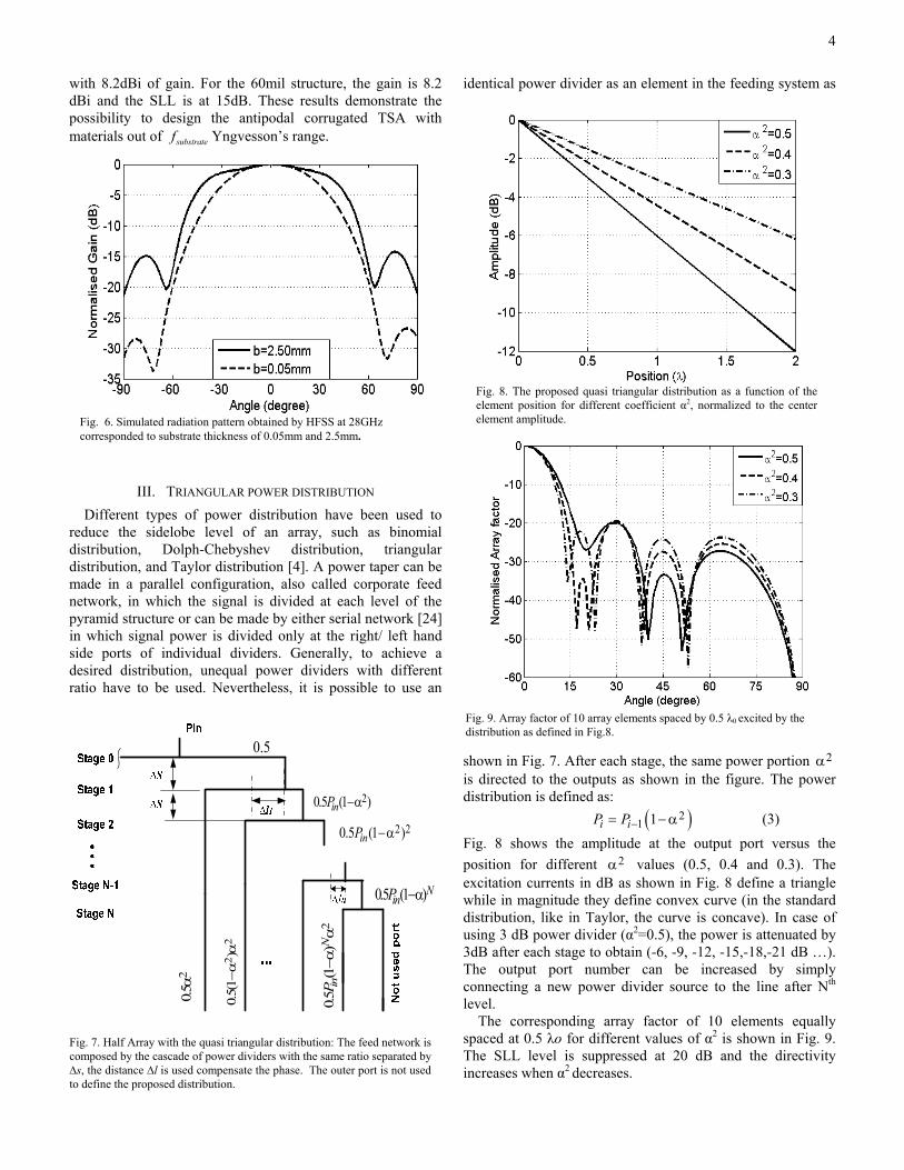
4
with 8.2dBi of gain. For the 60mil structure, the gain is 8.2 dBi and the SLL is at 15dB. These results demonstrate the possibility to design the antipodal corrugated TSA with materials out of substratef Yngvesson’s range.
III. TRIANGULAR POWER DISTRIBUTION
Different types of power distribution have been used to reduce the sidelobe level of an array, such as binomial distribution, Dolph-Chebyshev distribution, triangular distribution, and Taylor distribution [4]. A power taper can be made in a parallel configuration, also called corporate feed network, in which the signal is divided at each level of the pyramid structure or can be made by either serial network [24] in which signal power is divided only at the right/ left hand side ports of individual dividers. Generally, to achieve a desired distribution, unequal power dividers with different ratio have to be used. Nevertheless, it is possible to use an
identical power divider as an element in the feeding system as
shown in Fig. 7. After each stage, the same power portion 2 is directed to the outputs as shown in the figure. The power distribution is defined as:
21 1i iP P (3)
Fig. 8 shows the amplitude at the output port versus the
position for different 2 values (0.5, 0.4 and 0.3). The excitation currents in dB as shown in Fig. 8 define a triangle while in magnitude they define convex curve (in the standard distribution, like in Taylor, the curve is concave). In case of using 3 dB power divider (α2=0.5), the power is attenuated by 3dB after each stage to obtain (-6, -9, -12, -15,-18,-21 dB …). The output port number can be increased by simply connecting a new power divider source to the line after Nth level.
The corresponding array factor of 10 elements equally spaced at 0.5 λo for different values of α2 is shown in Fig. 9. The SLL level is suppressed at 20 dB and the directivity increases when α2 decreases.
Fig. 6. Simulated radiation pattern obtained by HFSS at 28GHz corresponded to substrate thickness of 0.05mm and 2.5mm.
20.5 (1 )inP
20.
5
0.5
22
0.5(
1)
2 20.5 (1 )inP
0.5 (1 )NinP
20.
5(1
)NinP
Fig. 7. Half Array with the quasi triangular distribution: The feed network is composed by the cascade of power dividers with the same ratio separated by ∆s, the distance ∆l is used compensate the phase. The outer port is not used to define the proposed distribution.
Fig. 9. Array factor of 10 array elements spaced by 0.5 λ0 excited by the distribution as defined in Fig.8.
Fig. 8. The proposed quasi triangular distribution as a function of the element position for different coefficient α2, normalized to the center element amplitude.
5
The proposed power divider is used to define the current distribution of a 10 element array. As shown in Fig. 10, the circuit is built of equal power divider T-junctions. To define the initial design parameters of the T junction with inductive matching post, a set of curves is used. This set has been generated with the use of a FEM software package [25]. To connect different power dividers, bends with posts are used. The initial parameters of the T junction are DT=0.1mm and
PT=0.8mm, and for the corner via are Dc=0.4mm and Pcx=Pcy=1.1mm. To equalize phase shifts at the output ports, differential length (∆li) phase shifters are used. Fig.10 presents the E-field distribution along the designed structure containing 3dB-T power divider. As shown in the figure, the power is divided by two after each stage. The phases are thus equal at the output ports. When port 1 is exited to the output ports starting by the outer port (port2) to the central one (port7) as shown in Fig. 10-, simulated transmission coefficients in Fig. 11 are reported and compared with intending ones (namely, -6,-9,-12,-15 and -18 dB). All transmission coefficients fluctuate around the ideal coupling factor in the band of 24 to 28GHz. Over this band, the return loss is less than -20 dB. The differences of phase shift between adjacent outputs are shown in Fig. 12. The structure provides in-phase shift output ports with 7 degrees error from 23 to 28GHz. The proposed series feeder is used to feed antipodal LTSAs array. The antenna design shown in Fig. 13 is fabricated as a fully integrated feed. In principle, the last branch is not used to define the proposed quasi-triangular amplitude taper. In fact, the power ratio fed to the port 2 and 3 are the same. However, to ensure the lossless nature of this power divider, the two outputs in the outer sides are used to feed more array elements. The structure is milled by using a laser micromachining technique with very tight tolerances. The overall antenna size is of 71x96 mm2 involving SIW microstrip transitions.
The measured radiation pattern at 28 GHz is shown in Fig.
14 and compared to the simulated one. Both measurement and simulation are in good agreement. The gain of the main lobe is measured at 19.25 dBi with a 3 dB beamwidth of 10 degrees. There is a difference of 18.86 dB between the main beam and side lobes observed at 16 degrees. The H-plane pattern remains almost unchanged (56 degrees) compared to a single element, except for a slight decrease in SSL.
TP
TD
cD cyP
cxP
Fig. 10. E-field magnitude distribution obtained by HFSS at 28GHz along
the Power divider constructed by 3 dB T junctions and bends.
Fig. 11. Couplings coefficient between the input port and the output ports as well as return loss performances.
Fig. 12. The phase shifts differences between adjacent outputs.
Fig. 13 . 1x12 antipodal LTSA array antenna feed by quasi triangular power divider

6
VI. CONCLUSION
A very compact and high performance corrugated antipodal antenna has been proposed, studied, fabricated, and measured. Measured results meet the proposed design specifications, which are in good agreement with simulated results. A wideband H-plane waveguide serial divider was designed to achieve in-phase and non-equal amplitude distributions. This power divider is used to generate the proposed simple quasi-
triangular distribution and can be used to achieve various amplitude distributions. The 12-way power divider was used to feed an antipodal LTSA array antenna. Experiments at 28 GHz have confirmed the generation of the desired distribution.
ACKNOWLEDGMENT
The authors are grateful to Traian Antonescu, Steve Dubé and Jules Gauthier for their collaborations during the fabrication process of the structures, and also Maxime Thibault for measurements in our anechoic chamber. The authors wish to acknowledge the financial support of the Natural Sciences and Engineering Research Council of Canada.
REFERENCES [1] R. Bayderkhani and H. R. Hassani, “Low sidelobe wideband series fed
double dipole microstrip antenna array,” IEICE Electron. Express, Vol. 6, No. 20, pp.1462-1468, 2009.
[2] D.L. Brown and E. Rammos, “Communication satellite requirements for the year 2000 and beyond,” Colloquium on Satellite Antenna Technology in the 21st Century, 12 Jun 1991 pp.1-2.
[3] F. Kolak and C. Eswarappa, “A Low Profile 77 GHz Three Beam Antenna for Automotive Radar,” 2001 IEEE MTT-S International Microwave Symposiu , pp. 1107 – 1110.
[4] R.J. Mailloux, Phased Array Antenna Handbook. Artech House, second edition, 2005.
[5] S.Yang, A. Elsherbini, S. Lin, A.E. Fathy, “A highly efficient Vivaldi antenna array design on thick substrate and fed by SIW structure with integrated GCPW feed,” 2007 Antennas and Propagation Society International Symposium, pp. 1985- 988 .
[6] K. S. Yngvesson, T. L. Korzeniowski, Y. S. Kim, E.L. Kollberg and J. F. Johansson, “The Tapered Slot Antema - A New Integrated Element for MM Wave Applications”, IEEE Trans. Microwave Theory and Tech., Vol.37, No.2 pp.365-374, Feb. 1989.
[7] P. R. Acharya, J. Johansson, and E. L. Kollberg,“Slotline antenna for millimeter and sub millimeter wavelength, ” Proc. 20th Eur. Microwave Conf, Budapest, Hungary, Sep. 1990, pp.353-358.
[8] P. R. Acharya, H. Ekstrom, S. S. Gearhart, S. Jacobsson, J. F. Johansson, E. L. Kollberg, G. M. Rebeiz, “Tapered Slotline Antenna at 802GHz” IEEE Trans. Microwave Theory and Tech., Vol.41, No. 10, pp.1715-1719, Oct. 1993.
[9] S. Sugawara, Y. Maita, K. Adachi, K. Mori, K. Mizuno, “ Characteristics of a MM-Wave Tapered Slot Antenna with Corrugated Edges,” IEEE Trans. Microwave Theory and Tech., pp. 533-536; June 1998.
[10] Hiroyasu Sato et aI., “Broadband FDTD Analysis of Fermi Antenna with Narrow Width Substrate,” IEEE Antenna & Propagat. Society Int. Symp.2003, Vol.1, pp. 261-264, 2003.
[11] Y. Venot, K. Schuler and W. Wiesbeck , “Tapered Slot Antenna for LTCC MultilayerSubstrate Integration in mm-Wave Applications ,” INICA-2003, ITG-Conference on Antennas, ITGFuchbereicht, Berlin Germany, September 17-19, 2003, pp. 49-52.
[12] Z. C. Hao, W. Hong, J. X. Chen, X. P. Chen, and K. Wu, “A novel feeding technique for antipodal linearly tapered Slot Antenna Array,” IEEE IMS 2005, Long Beach, California, pp.1641-1644, June 12-17, 2005.
[13] Y.J. Chen, W. Hong and K. Wu, “ Design of a Monopulse Antenna Using a Dual V-Type Linearly Tapered Slot Antenna,” IEEE trans. on Ant. and Prop. vol. 56, no. 9, p. 2903-2909 Sept 2008.
[14] B. Li, L. Dong, and J-C Zhao, “The research of broadband millimeter-wave vivaldi array antenna using SIW technique,” ICMMT 2010 Proc., pp 997-1000.
[15] S. Lin, S. Yang, A. E. Fathy, and A. Elsherbini "Development of A Novel UWB Vivaldi Antenna Array Using SIW Technology," Progress In Electromagnetics Research, pp.369–384, 2009.
[16] S. Yang, S.H. Suleiman, and A.E. Fathy, “Low profile multi-layer slotted Substrate Integrated Waveguide (SIW) array antenna with folded feed network for mobile DBS applications,” 2007 Antennas and Propagation Society International Symposium, Page(s): 473-476.
[17] E. Moldovan, R.G. Bosisio, and K. Wu, W-band multiport substrate-integrated waveguide circuits, IEEE Trans Microwave Theory Tech.,54, pp- 625–632. 2006.
[18] K. Kuhlmann, K. Rezer, and A.F. Jacob, “Circularly polarized substrate-integrated waveguide antenna array at Ka-band,” Proceedings of German Microwave Conference, Hamburg, Germany, March 2008, pp. 471–474.
[19] G. H. Zhai, W. Hong, K. Wu, J. X. Chen, P. Chen, J. Wei, and H. J. Tang, “Folded half mode substrate integrated waveguide 3 dB coupler,” IEEE Microw. Wireless Compon. Lett., vol. 18, no. 8, pp. 512–514, Aug. 2008.
[20] Z. G. Wang, X. Q. Li, S. P. Zhou, B. Yan, R. M. Xu and W. G. Lin, “ Half Mode Substrate Integrated Folded Waveguide (Hmsifw) And Partial H-Plane Bandpass Filter,” Progress In Electromagnetics Research, PIER, pp 2010.
[21] F. Xu, K. Wu, and X. P. Zhang, “Periodic leaky-wave antenna for millimeter waves based on substrate integrated waveguide,” IEEE Trans. Antennas and Propagation.
[22] P.S. HALL, “Feed radiation effects in sequentially rotated microstrippatch arrays,” Electron. Lett., pp. 877-878. 1987.
[23] R.A. PuceL, D. Masse, and C.P. Hartwig, “Losses in microstrip,” IEEE IEEE Trans. Microwave Theory and Tech, pp. 342-350 1064, 1968.
[24] K. J. Russell, “Microwave power combining techniques,” IEEE Trans. Microwave Theory Tech., vol. MTT-27, pp. 472 - 478, 1979.
[25] S. Germain, D. Deslandes, K. Wu, “Development of substrate integrated waveguide power dividers,” 2003 Canadian Conference on Electrical and Computer Engineering, pp.1921-1924, May 4-7, Montréal, Canada.
Fig. 14. Simulated and measured radiation patterns of the designed 1x12 antipodal LTSAs array spaced by 0.75 λ0 at 28GHz.