Thesis presentation
43
Aix-Marseille Université Institut Matériaux Microélectronique Nanosciences de Provence Ecole Doctorale Physique et Sciences de la Matière Université de Monastir Ecole doctorale Matériaux, Dispositifs et Microsystèmes Croissance et propriétés électroniques et optiques des nanostructures à base de SiGe Maher Nafouti July 29 th , 2016 Deterministic fabrication of Si and SiGe-based nanostructures via solid state dewetting of thin silicon film on insulator
-
Upload
meher-naffouti -
Category
Technology
-
view
85 -
download
0
Transcript of Thesis presentation
Aix-Marseille UniversitéInstitut Matériaux Microélectronique Nanosciences de Provence
Ecole Doctorale Physique et Sciences de la MatièreUniversité de Monastir
Ecole doctorale Matériaux, Dispositifs et Microsystèmes
Croissance et propriétés électroniques et optiques des nanostructures à base de SiGe
Maher NafoutiJuly 29th, 2016
Deterministic fabrication of Si and SiGe-based nanostructures via solid state dewetting of
thin silicon film on insulator
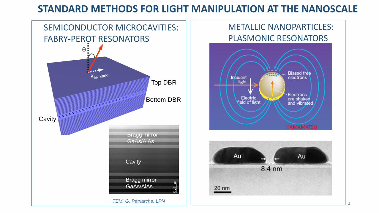
STANDARD METHODS FOR LIGHT MANIPULATION AT THE NANOSCALE
Top DBR
Bottom DBR
θ
SEMICONDUCTOR MICROCAVITIES: FABRY-PEROT RESONATORS
METALLIC NANOPARTICLES:PLASMONIC RESONATORS
HAMAMATSU
Bragg mirror
GaAs/AlAs
Cavity
Bragg mirror
GaAs/AlAs
TEM, G. Patriarche, LPN
Cavity
2
STANDARD METHODS FOR LIGHT MANIPULATION AT THE NANOSCALE
PURCELL EFFECT: enhancement of spontaneous emission rate of two-level system
𝐹𝑃 ∝𝑄
𝑉
QUALITY FACTOR (“photon life”)
MODE VOLUME
METALLIC NANOPARTICLES:PLASMONIC RESONATORS
Fan, SCIENCE 2010
V<<l3
Q~100
….but very small particles suffer from significant ohmic losses, which scale with volume V.
SEMICONDUCTOR MICROCAVITIES: “FABRY-PEROT” RESONATORS
Vahala NATURE 2003
Q=103-109
V>>l3
….small ohmic losses and very large Q but relatively large modal volume V.
Limitation techniques!!
3
Garcıa-Etxarri OPT. EXP 2011Kuznetsov, SCI. REP 2012
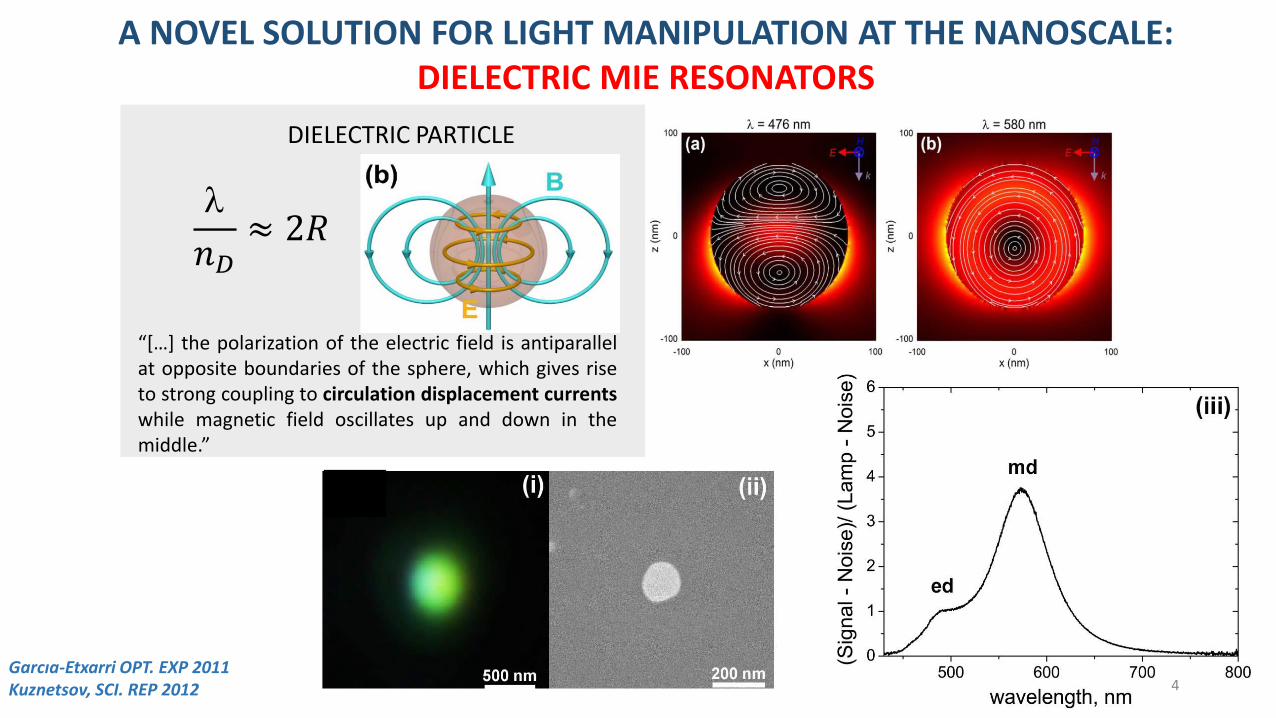
A NOVEL SOLUTION FOR LIGHT MANIPULATION AT THE NANOSCALE:DIELECTRIC MIE RESONATORS
DIELECTRIC PARTICLE
l
𝑛𝐷≈ 2𝑅
“[…] the polarization of the electric field is antiparallelat opposite boundaries of the sphere, which gives riseto strong coupling to circulation displacement currentswhile magnetic field oscillates up and down in themiddle.”
4
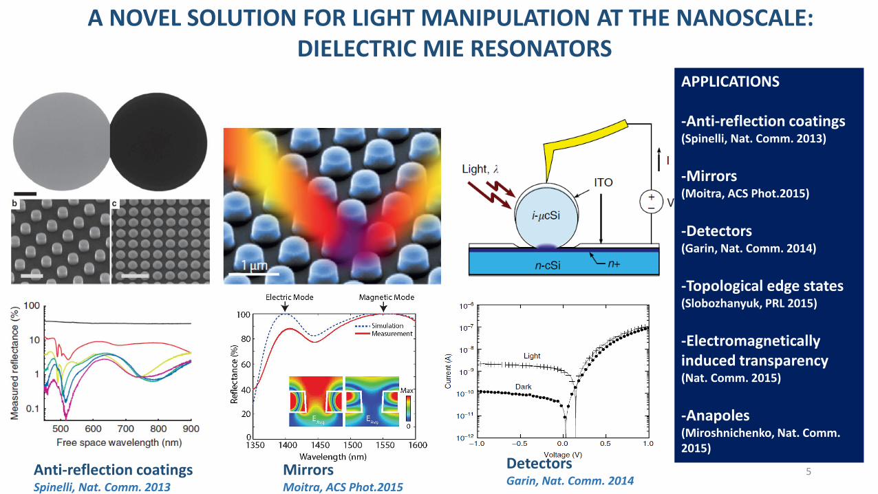
A NOVEL SOLUTION FOR LIGHT MANIPULATION AT THE NANOSCALE:DIELECTRIC MIE RESONATORS
Anti-reflection coatingsSpinelli, Nat. Comm. 2013
MirrorsMoitra, ACS Phot.2015
DetectorsGarin, Nat. Comm. 2014
APPLICATIONS
-Anti-reflection coatings(Spinelli, Nat. Comm. 2013)
-Mirrors(Moitra, ACS Phot.2015)
-Detectors(Garin, Nat. Comm. 2014)
-Topological edge states(Slobozhanyuk, PRL 2015)
-Electromagnetically induced transparency(Nat. Comm. 2015)
-Anapoles(Miroshnichenko, Nat. Comm. 2015)
5
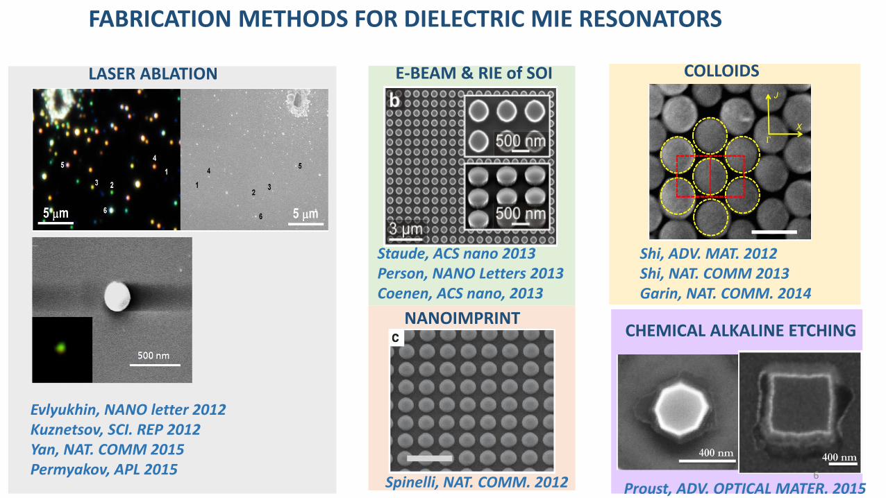
FABRICATION METHODS FOR DIELECTRIC MIE RESONATORS
Evlyukhin, NANO letter 2012Kuznetsov, SCI. REP 2012Yan, NAT. COMM 2015 Permyakov, APL 2015
LASER ABLATION E-BEAM & RIE of SOI
Staude, ACS nano 2013Person, NANO Letters 2013Coenen, ACS nano, 2013
Spinelli, NAT. COMM. 2012
NANOIMPRINT
COLLOIDS
Shi, ADV. MAT. 2012Shi, NAT. COMM 2013Garin, NAT. COMM. 2014
CHEMICAL ALKALINE ETCHING
Proust, ADV. OPTICAL MATER. 20156
Outline
I: Dewetting of thin Silicon layer on insulator
II: Silicon-Based Mie Resonators via Silicon-on-Insulator dewetting
III: Templated solid-state dewetting to controllably produce complex patterns
IV: Fabrication of core-half shell nanostructures based on SiGe
7
Outline
II: Silicon-Based Mie Resonators via Silicon-on-Insulator Dewetting
III: Templated solid-state dewetting to controllably produce complex patterns
IV: Fabrication of core-half shell nanostructures via UTSOI dewettingand Ge condensation
I: Dewetting of thin Silicon layer on insulator
8
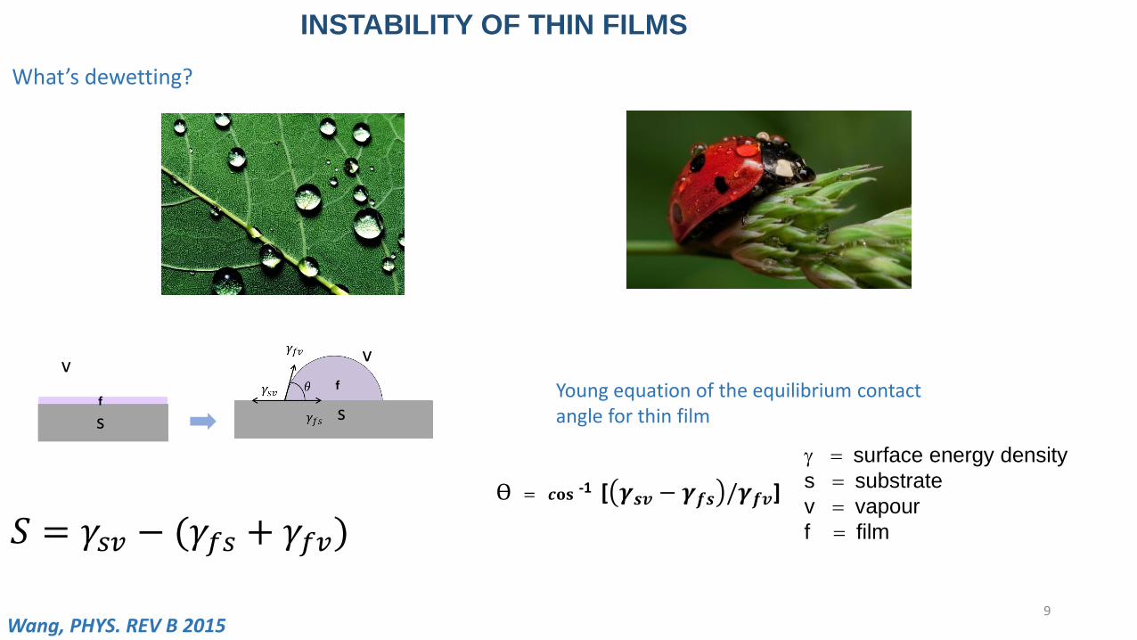
Wang, PHYS. REV B 2015
Young equation of the equilibrium contact angle for thin film
= surface energy density
s = substrate
v = vapour
f = film𝑆 = 𝛾𝑠𝑣 − (𝛾𝑓𝑠 + 𝛾𝑓𝑣)
What’s dewetting?
INSTABILITY OF THIN FILMS
s
f
v
sf
v
Ɵ = 𝒄𝐨𝐬 -1 [ 𝜸𝒔𝒗 − 𝜸𝒇𝒔 /𝜸𝒇𝒗]
9
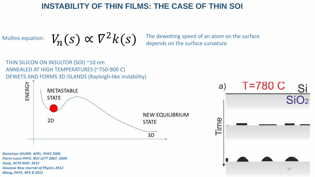
THIN SILICON ON INSULTOR (SOI) ~10 nm ANNEALED AT HIGH TEMPERATURES (~750-900 C)DEWETS AND FORMS 3D ISLANDS (Rayleigh-like instability)
Danielson JOURN. APPL. PHYS 2006 Pierre-Louis PHYS. REV LETT 2007, 2009Jiang, ACTA MAT. 2012Aouassa New Journal of Physics 2012Wang, PHYS. REV B 2015
INSTABILITY OF THIN FILMS: THE CASE OF THIN SOI
Mullins equation: 𝑉𝑛(𝑠) ∝ 𝛻2𝑘(𝑠) The dewetting speed of an atom on the surface depends on the surface curvature
ENER
GY
METASTABLESTATE
NEW EQUILIBRIUMSTATE2D
3D
10
BUSSMAN New Journal of Physics 2011
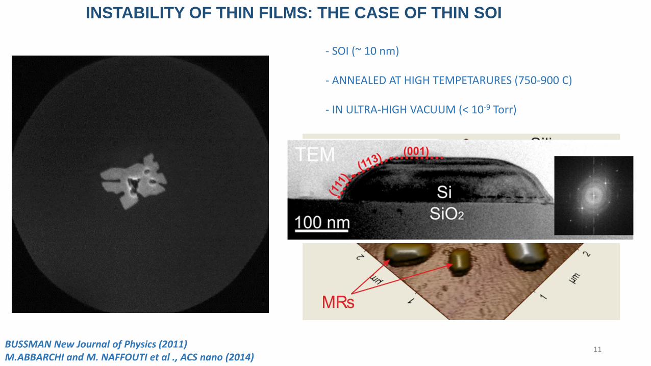
- SOI (~ 10 nm)
- ANNEALED AT HIGH TEMPETARURES (750-900 C)
- IN ULTRA-HIGH VACUUM (< 10-9 Torr)
INSTABILITY OF THIN FILMS: THE CASE OF THIN SOI
BUSSMAN New Journal of Physics (2011)M.ABBARCHI and M. NAFFOUTI et al ., ACS nano (2014)
11
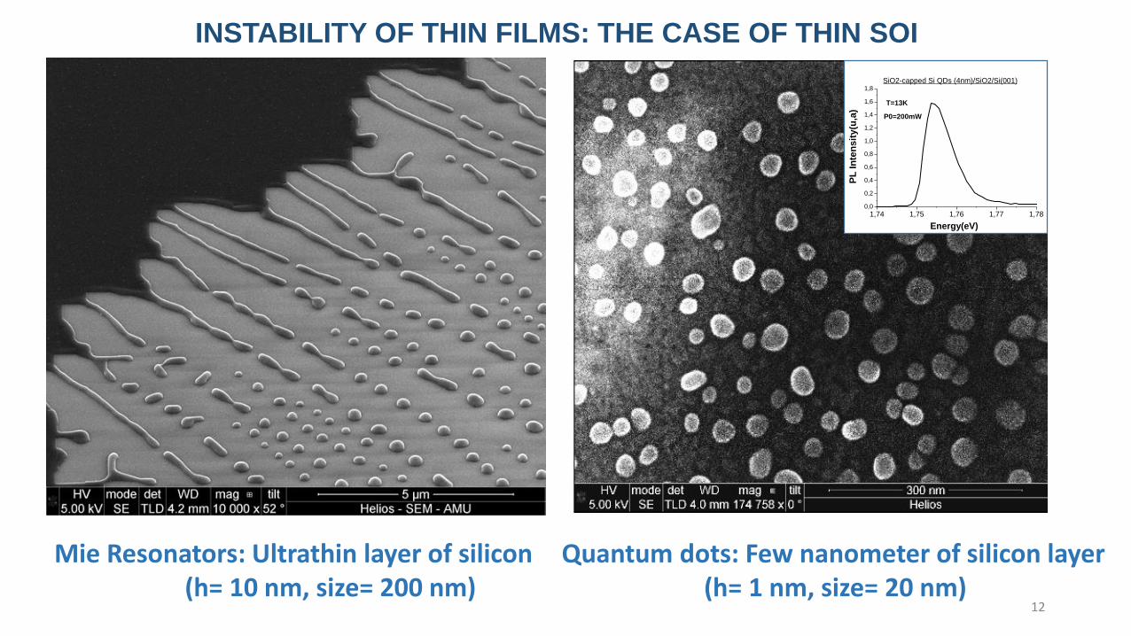
Mie Resonators: Ultrathin layer of silicon(h= 10 nm, size= 200 nm)
1,74 1,75 1,76 1,77 1,780,0
0,2
0,4
0,6
0,8
1,0
1,2
1,4
1,6
1,8
PL
In
ten
sit
y(u
,a)
Energy(eV)
SiO2-capped Si QDs (4nm)/SiO2/Si(001)
T=13K
P0=200mW
Quantum dots: Few nanometer of silicon layer(h= 1 nm, size= 20 nm)
INSTABILITY OF THIN FILMS: THE CASE OF THIN SOI
12
Outline
II: Silicon-Based Mie Resonators via Silicon-on-Insulator Dewetting
III: Templated solid-state dewetting to controllably produce complex patterns
IV: Fabrication of core-half shell nanostructures via UTSOI dewettingand Ge condensation
I: Dewetting of thin Silicon layer on insulator
13
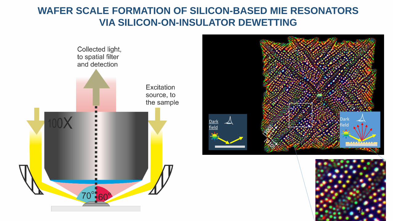
Darkfield
Darkfield
WAFER SCALE FORMATION OF SILICON-BASED MIE RESONATORS
VIA SILICON-ON-INSULATOR DEWETTING
14
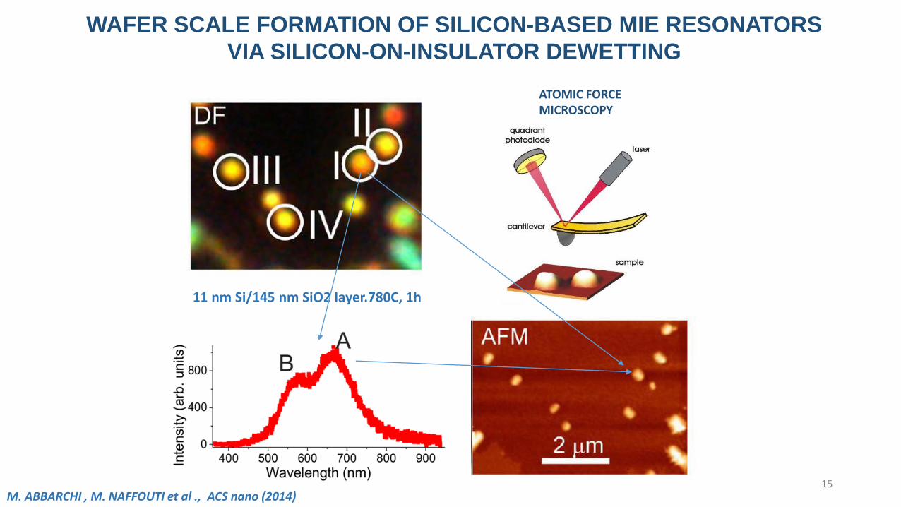
ATOMIC FORCE MICROSCOPY
WAFER SCALE FORMATION OF SILICON-BASED MIE RESONATORS
VIA SILICON-ON-INSULATOR DEWETTING
780 C, 1h
11 nm Si/145 nm SiO2 layer.780C, 1h
15M. ABBARCHI , M. NAFFOUTI et al ., ACS nano (2014)
WAFER SCALE FORMATION OF SILICON-BASED MIE RESONATORS
VIA SILICON-ON-INSULATOR DEWETTING
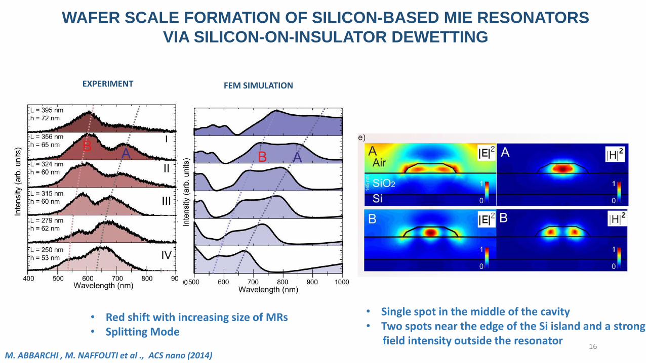
EXPERIMENT FEM SIMULATION
• Red shift with increasing size of MRs • Splitting Mode
• Single spot in the middle of the cavity• Two spots near the edge of the Si island and a strong
field intensity outside the resonator16
M. ABBARCHI , M. NAFFOUTI et al ., ACS nano (2014)
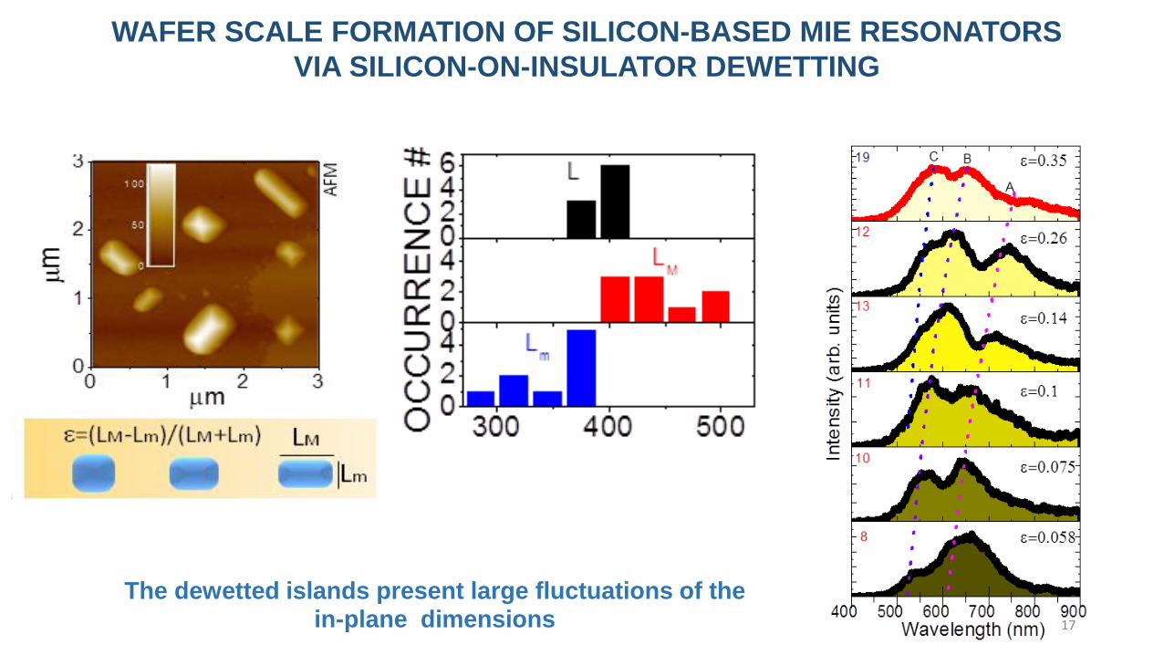
The dewetted islands present large fluctuations of the in-plane dimensions
WAFER SCALE FORMATION OF SILICON-BASED MIE RESONATORS
VIA SILICON-ON-INSULATOR DEWETTING
17
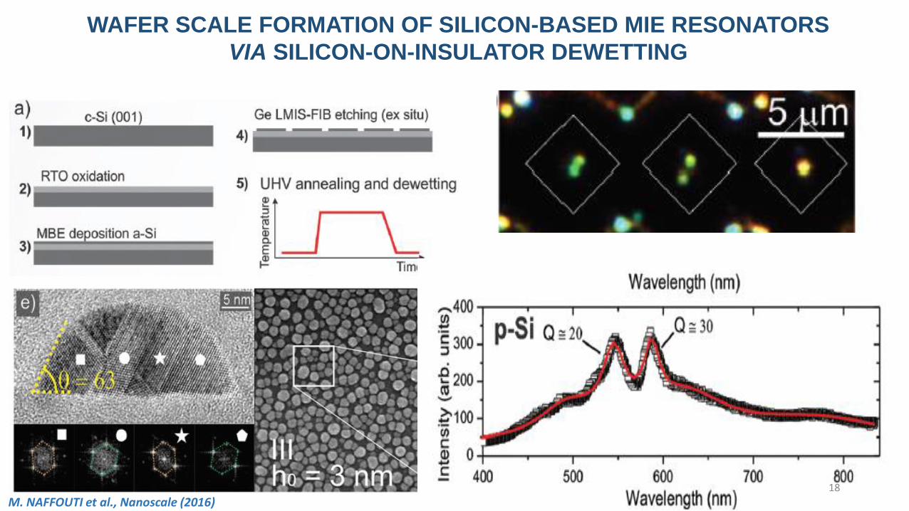
M. NAFFOUTI et al., Nanoscale (2016)
WAFER SCALE FORMATION OF SILICON-BASED MIE RESONATORS
VIA SILICON-ON-INSULATOR DEWETTING
18
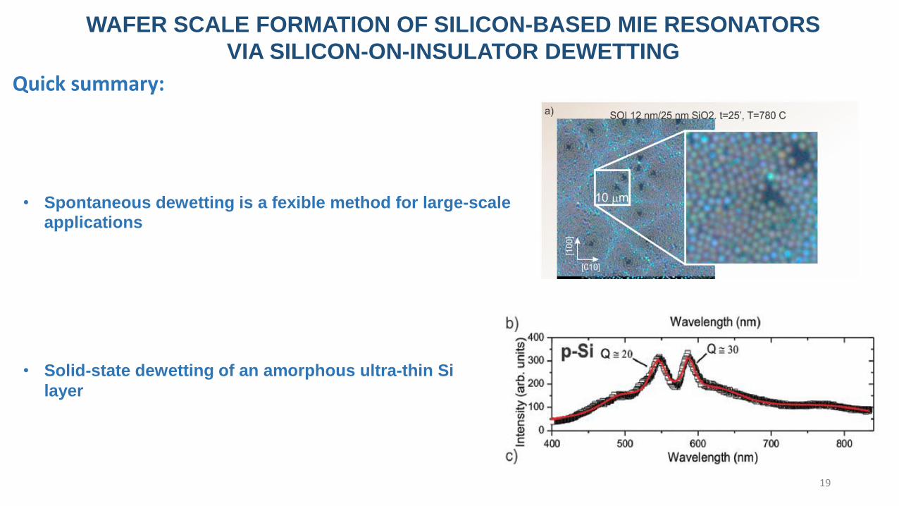
Quick summary:
• Spontaneous dewetting is a fexible method for large-scale
applications
• Solid-state dewetting of an amorphous ultra-thin Si
layer
WAFER SCALE FORMATION OF SILICON-BASED MIE RESONATORS
VIA SILICON-ON-INSULATOR DEWETTING
19
Outline
I: Dewetting of thin Silicon layer on insulator
II: Silicon-Based Mie Resonators via Silicon-on-Insulator Dewetting
III: Templated solid-state dewetting to controllably produce complex patterns
IV: Fabrication of core-half shell nanostructures via UTSOI dewettingand Ge condensation 20
TIME, TEMPERATURE
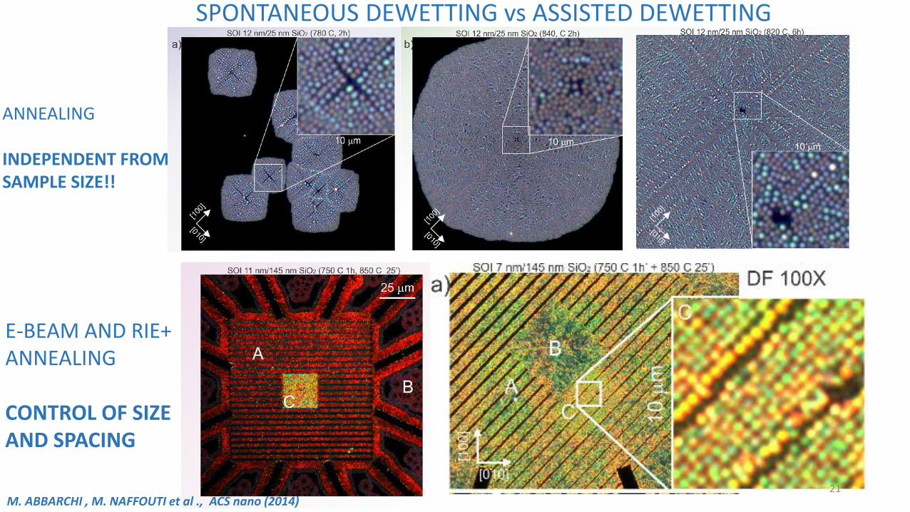
SPONTANEOUS DEWETTING vs ASSISTED DEWETTING
E-BEAM AND RIE+ANNEALING
CONTROL OF SIZEAND SPACING
ANNEALING
INDEPENDENT FROMSAMPLE SIZE!!
21M. ABBARCHI , M. NAFFOUTI et al ., ACS nano (2014)
Darkfield
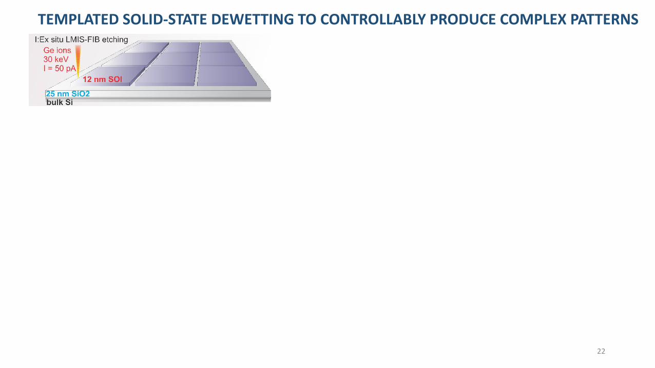
TEMPLATED SOLID-STATE DEWETTING TO CONTROLLABLY PRODUCE COMPLEX PATTERNS
22
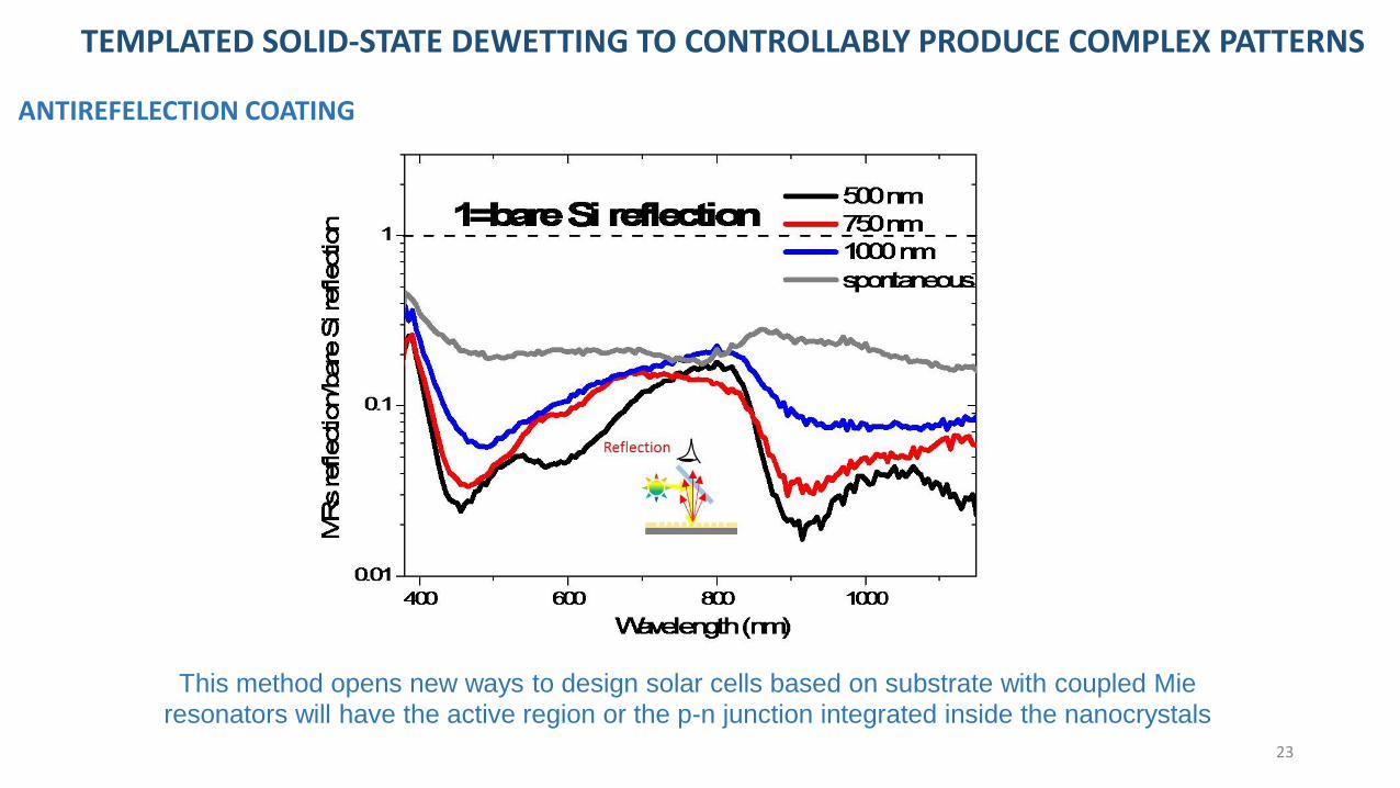
This method opens new ways to design solar cells based on substrate with coupled Mie
resonators will have the active region or the p-n junction integrated inside the nanocrystals
TEMPLATED SOLID-STATE DEWETTING TO CONTROLLABLY PRODUCE COMPLEX PATTERNS
ANTIREFELECTION COATING
23
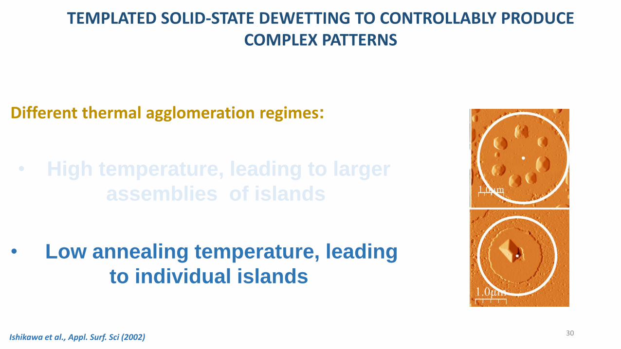
Ishikawa et al., Appl. Surf. Sci (2002)
TEMPLATED SOLID-STATE DEWETTING TO CONTROLLABLY PRODUCECOMPLEX PATTERNS
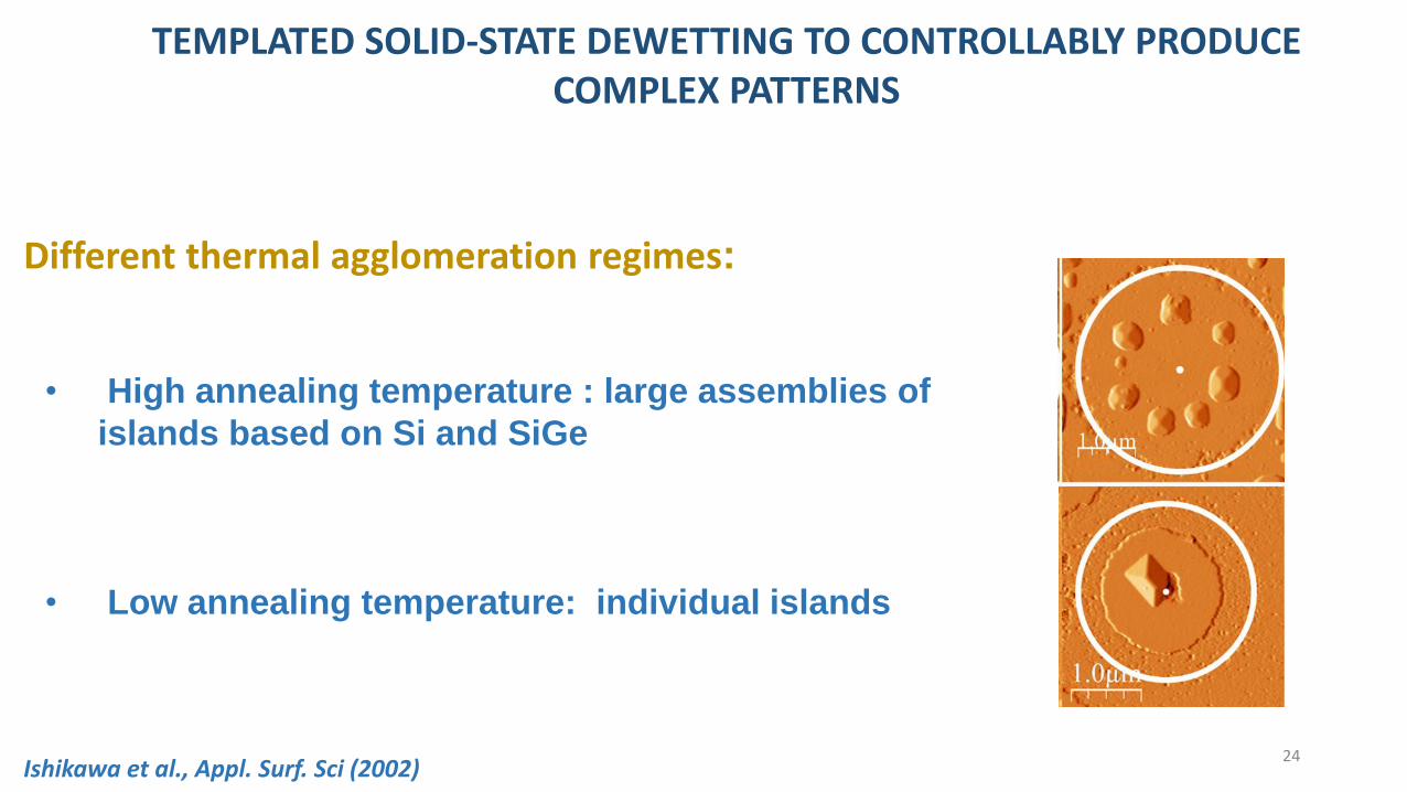
Different thermal agglomeration regimes:
• High annealing temperature : large assemblies of
islands based on Si and SiGe
• Low annealing temperature: individual islands
24
TEMPLATED SOLID-STATE DEWETTING TO CONTROLLABLY PRODUCECOMPLEX PATTERNS
25
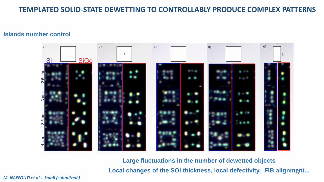
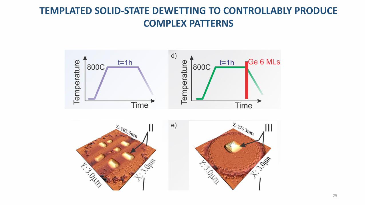
Large fluctuations in the number of dewetted objects
Local changes of the SOI thickness, local defectivity, FIB alignment...
Islands number control
M. NAFFOUTI et al., Small (submitted )
TEMPLATED SOLID-STATE DEWETTING TO CONTROLLABLY PRODUCE COMPLEX PATTERNS
26
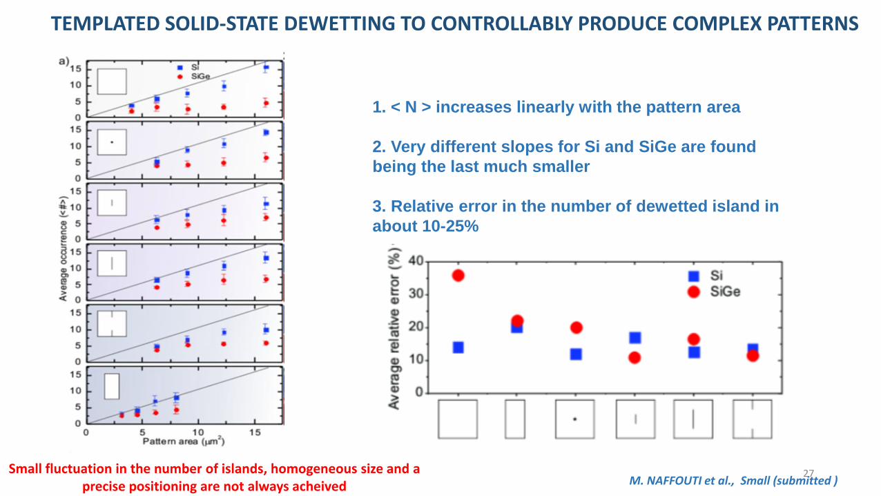
1. < N > increases linearly with the pattern area
2. Very different slopes for Si and SiGe are found
being the last much smaller
3. Relative error in the number of dewetted island in
about 10-25%
Small fluctuation in the number of islands, homogeneous size and a precise positioning are not always acheived M. NAFFOUTI et al., Small (submitted )
TEMPLATED SOLID-STATE DEWETTING TO CONTROLLABLY PRODUCE COMPLEX PATTERNS
27
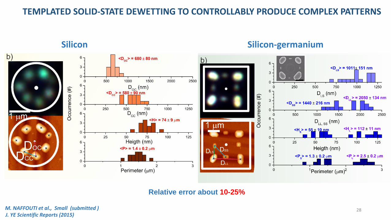
Silicon Silicon-germanium
Relative error about 10-25%
M. NAFFOUTI et al., Small (submitted )
TEMPLATED SOLID-STATE DEWETTING TO CONTROLLABLY PRODUCE COMPLEX PATTERNS
J. YE Scientific Reports (2015)28
TEMPLATED SOLID-STATE DEWETTING TO CONTROLLABLY PRODUCE COMPLEX PATTERNS
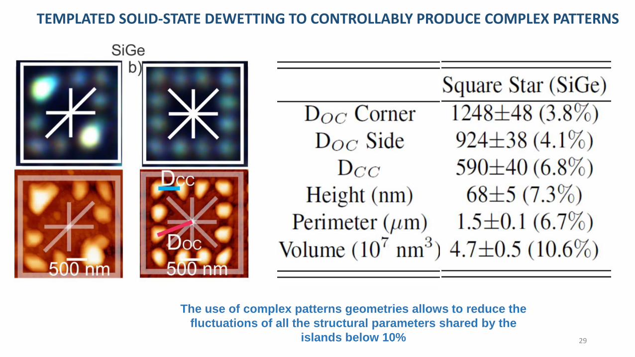
The use of complex patterns geometries allows to reduce the
fluctuations of all the structural parameters shared by the
islands below 10% 29
Ishikawa et al., Appl. Surf. Sci (2002)
TEMPLATED SOLID-STATE DEWETTING TO CONTROLLABLY PRODUCECOMPLEX PATTERNS
Different thermal agglomeration regimes:
• High temperature, leading to larger
assemblies of islands
• Low annealing temperature, leading
to individual islands
30
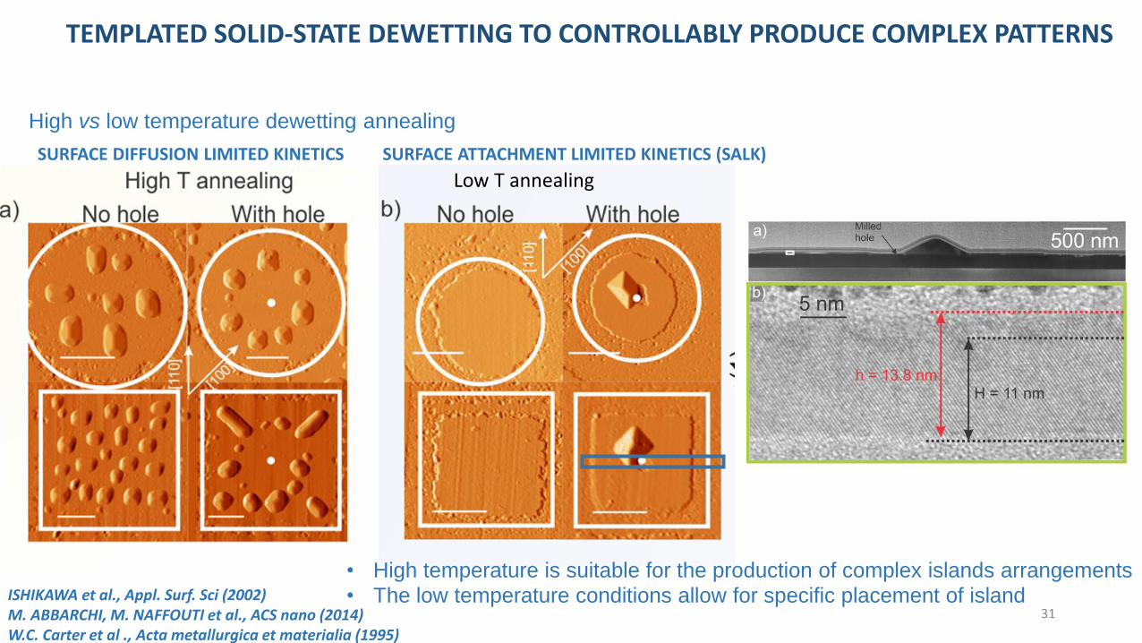
TEMPLATED SOLID-STATE DEWETTING TO CONTROLLABLY PRODUCE COMPLEX PATTERNS
Low T annealing
High vs low temperature dewetting annealing
• High temperature is suitable for the production of complex islands arrangements
• The low temperature conditions allow for specific placement of islandISHIKAWA et al., Appl. Surf. Sci (2002)M. ABBARCHI, M. NAFFOUTI et al., ACS nano (2014)W.C. Carter et al ., Acta metallurgica et materialia (1995)
SURFACE ATTACHMENT LIMITED KINETICS (SALK)SURFACE DIFFUSION LIMITED KINETICS
31
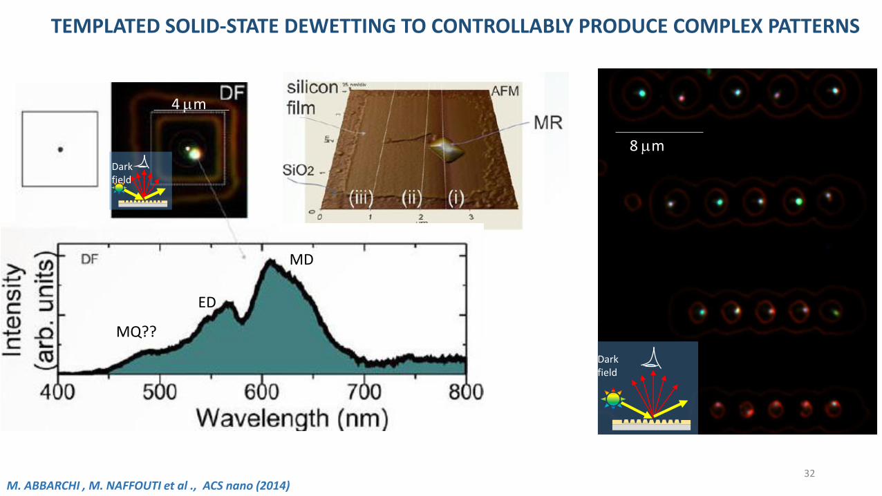
MD
ED
MQ??
4 mm
8 mm
Darkfield
Darkfield
TEMPLATED SOLID-STATE DEWETTING TO CONTROLLABLY PRODUCE COMPLEX PATTERNS
32M. ABBARCHI , M. NAFFOUTI et al ., ACS nano (2014)
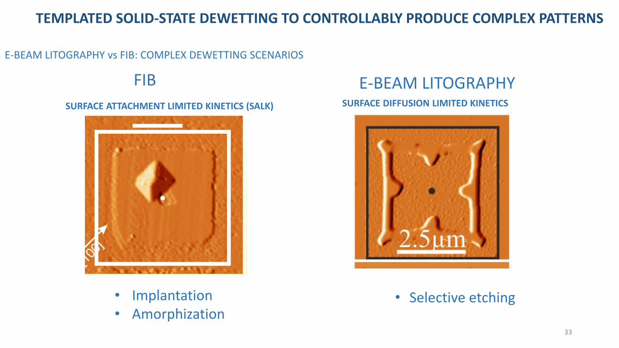
E-BEAM LITOGRAPHY vs FIB: COMPLEX DEWETTING SCENARIOS
E-BEAM LITOGRAPHYFIB
SURFACE ATTACHMENT LIMITED KINETICS (SALK) SURFACE DIFFUSION LIMITED KINETICS
TEMPLATED SOLID-STATE DEWETTING TO CONTROLLABLY PRODUCE COMPLEX PATTERNS
• Implantation• Amorphization
• Selective etching
33
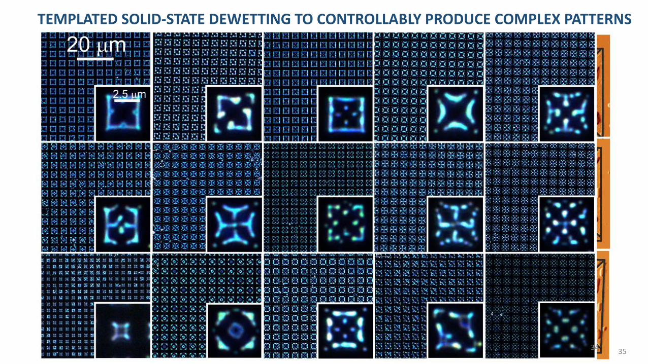
TEMPLATED SOLID-STATE DEWETTING TO CONTROLLABLY PRODUCE COMPLEX PATTERNS
3534
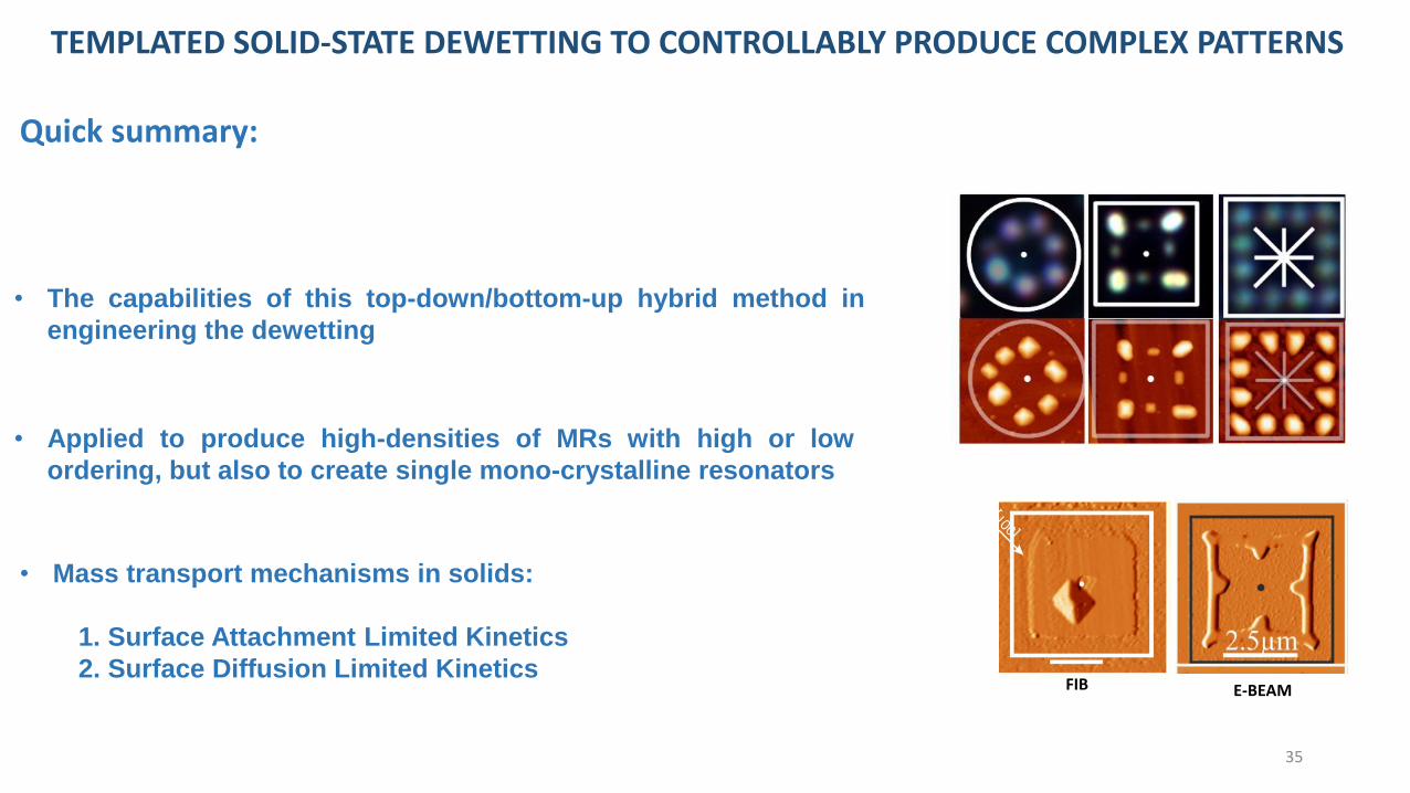
• The capabilities of this top-down/bottom-up hybrid method in
engineering the dewetting
• Applied to produce high-densities of MRs with high or low
ordering, but also to create single mono-crystalline resonators
Quick summary:
E-BEAMFIB
TEMPLATED SOLID-STATE DEWETTING TO CONTROLLABLY PRODUCE COMPLEX PATTERNS
• Mass transport mechanisms in solids:
1. Surface Attachment Limited Kinetics
2. Surface Diffusion Limited Kinetics
35
Outline
I: Dewetting of thin Silicon layer on insulator
II: Silicon-Based Mie Resonators via Silicon-on-Insulator Dewetting
III: Templated solid-state dewetting to controllably produce complex patterns
IV: Fabrication of core-half shell nanostructures via UTSOI dewettingand Ge condensation
36
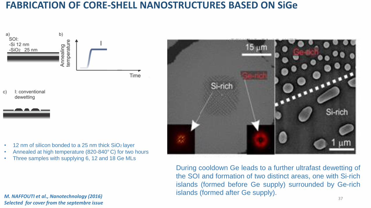
FABRICATION OF CORE-SHELL NANOSTRUCTURES BASED ON SiGe
• 12 nm of silicon bonded to a 25 nm thick SiO2 layer
• Annealed at high temperature (820-840° C) for two hours
• Three samples with supplying 6, 12 and 18 Ge MLs
During cooldown Ge leads to a further ultrafast dewetting of
the SOI and formation of two distinct areas, one with Si-rich
islands (formed before Ge supply) surrounded by Ge-rich
islands (formed after Ge supply).M. NAFFOUTI et al., Nanotechnology (2016)Selected for cover from the septembre issue
37
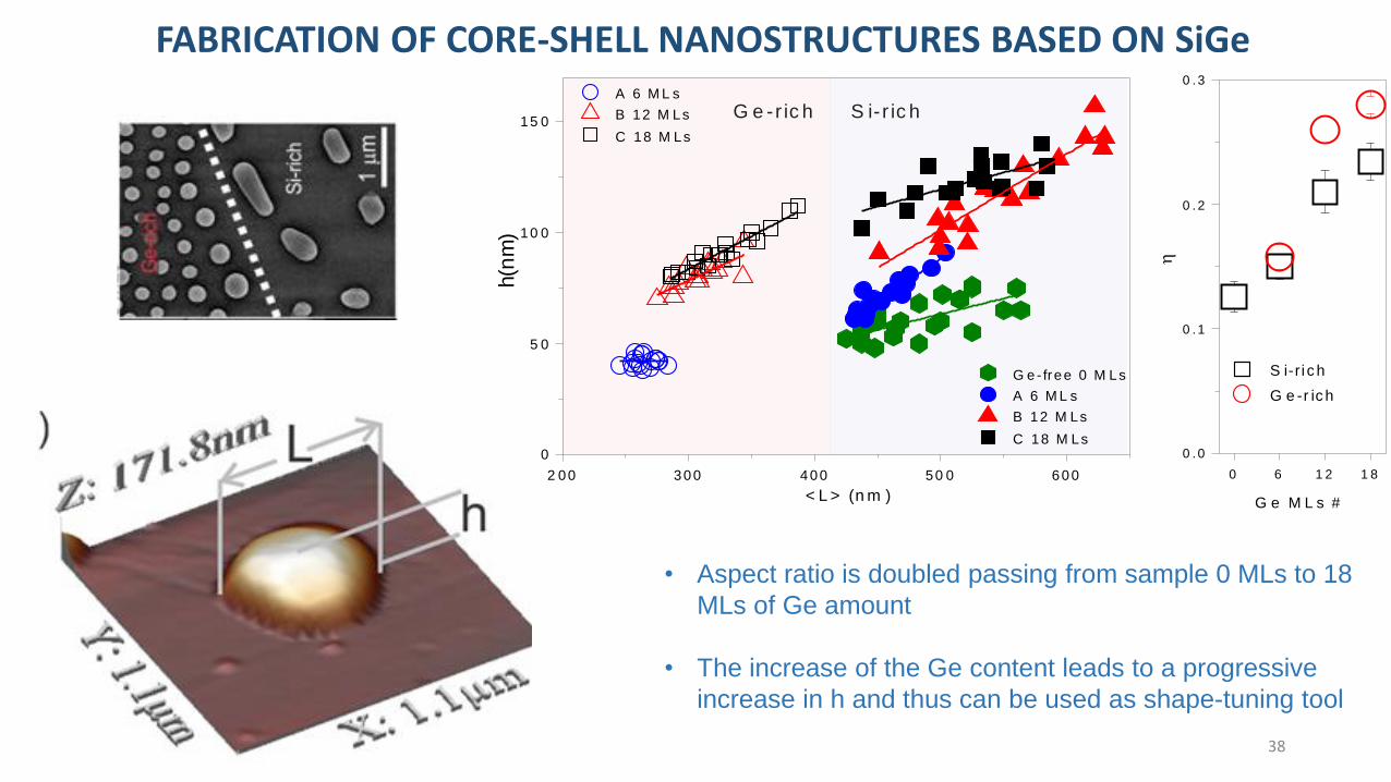
• Aspect ratio is doubled passing from sample 0 MLs to 18
MLs of Ge amount
• The increase of the Ge content leads to a progressive
increase in h and thus can be used as shape-tuning tool
FABRICATION OF CORE-SHELL NANOSTRUCTURES BASED ON SiGea ) b )
2 00 300 400 50 0 600
0
5 0
10 0
15 0
h(n
m)
< L > (n m )
G e- free 0 M Ls
A 6 M L s
B 12 M Ls
C 18 M Ls
A 6 M L s
B 12 M Ls
C 18 M Ls
0 6 1 2 1 8
0 .0
0 .1
0 .2
0 .3
G e M L s #
S i-r i c h
G e -r ic h
h
S i- r ic hG e -r ic h
38
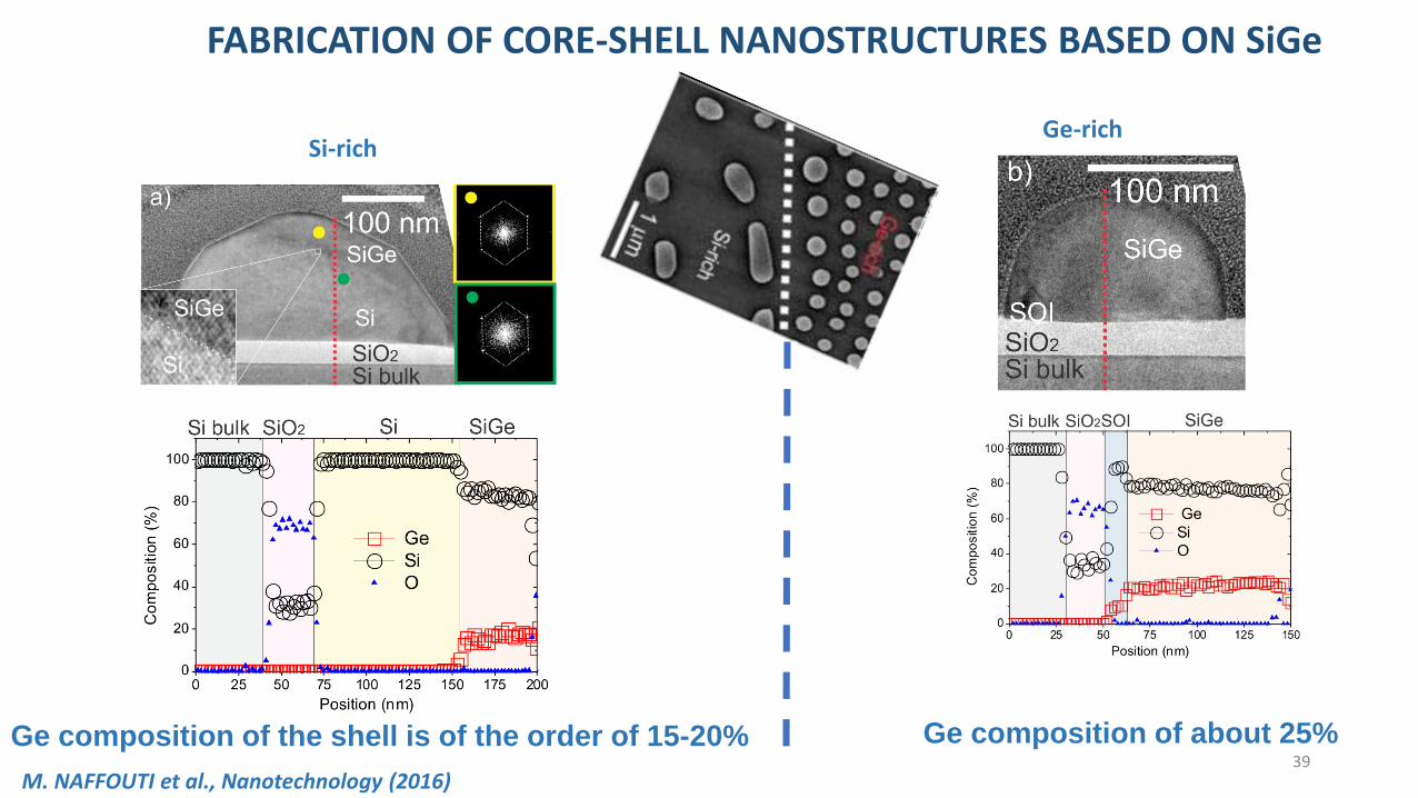
Si-rich
M. NAFFOUTI et al., Nanotechnology (2016)
Ge composition of the shell is of the order of 15-20% Ge composition of about 25%
Ge-rich
FABRICATION OF CORE-SHELL NANOSTRUCTURES BASED ON SiGe
39
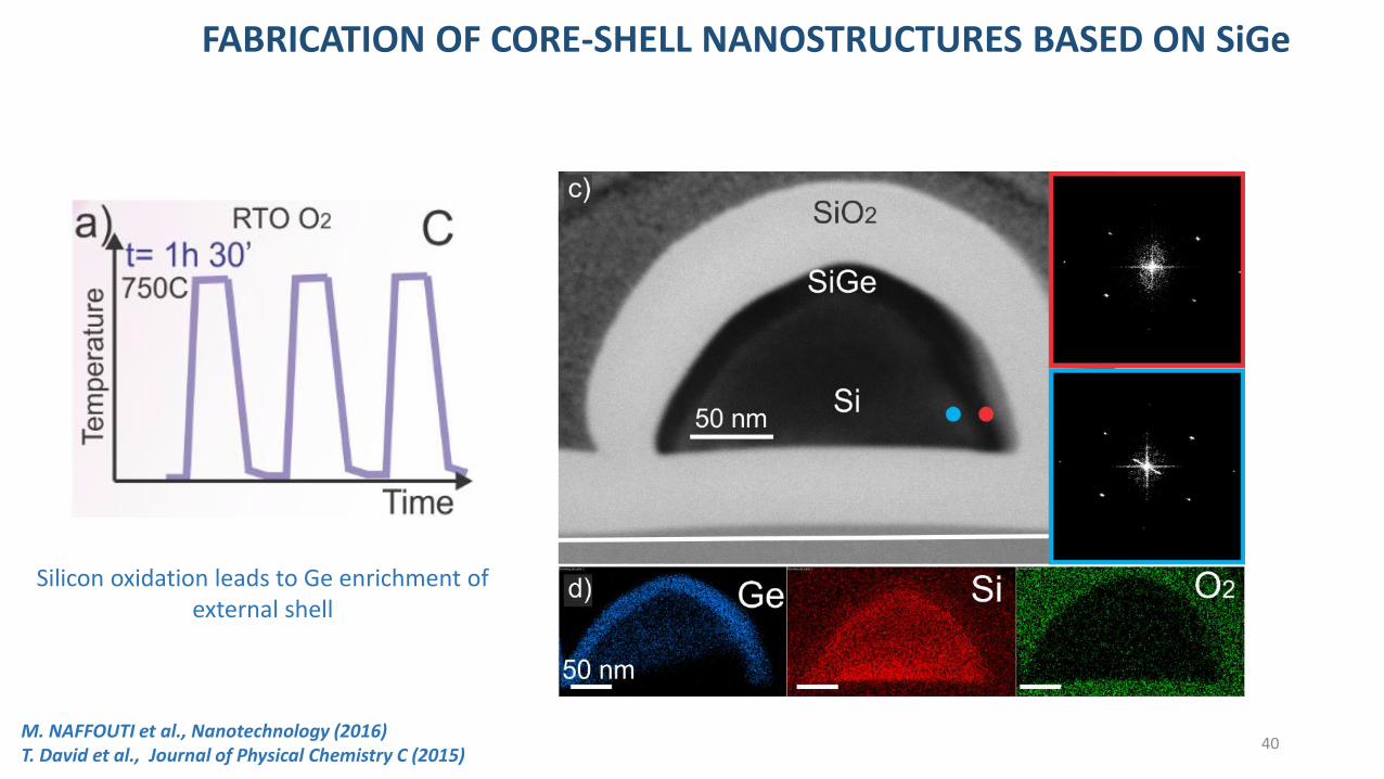
Silicon oxidation leads to Ge enrichment of external shell
M. NAFFOUTI et al., Nanotechnology (2016)T. David et al., Journal of Physical Chemistry C (2015)
FABRICATION OF CORE-SHELL NANOSTRUCTURES BASED ON SiGe
40
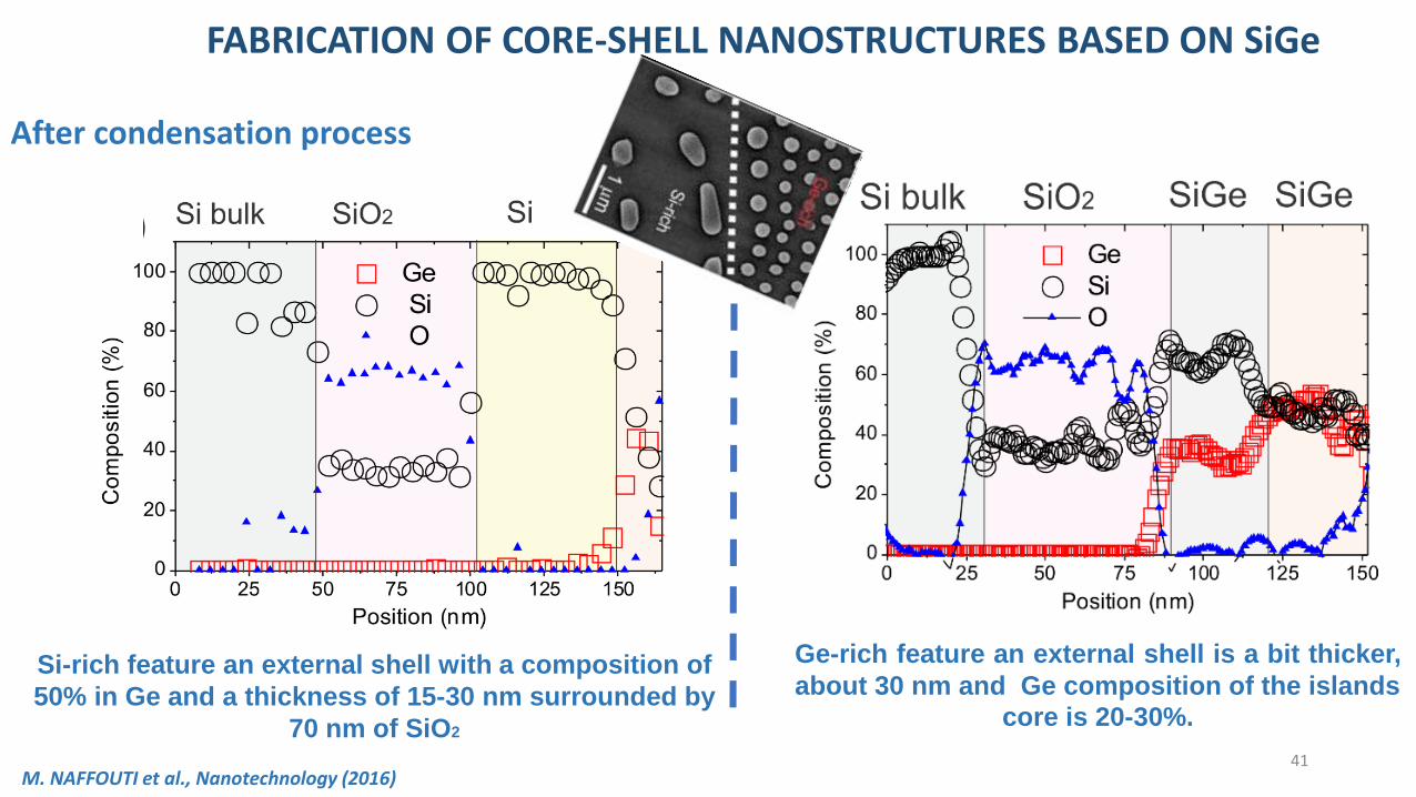
After condensation process
Ge-rich feature an external shell is a bit thicker,
about 30 nm and Ge composition of the islands
core is 20-30%.
Si-rich feature an external shell with a composition of
50% in Ge and a thickness of 15-30 nm surrounded by
70 nm of SiO2
M. NAFFOUTI et al., Nanotechnology (2016)
FABRICATION OF CORE-SHELL NANOSTRUCTURES BASED ON SiGe
41
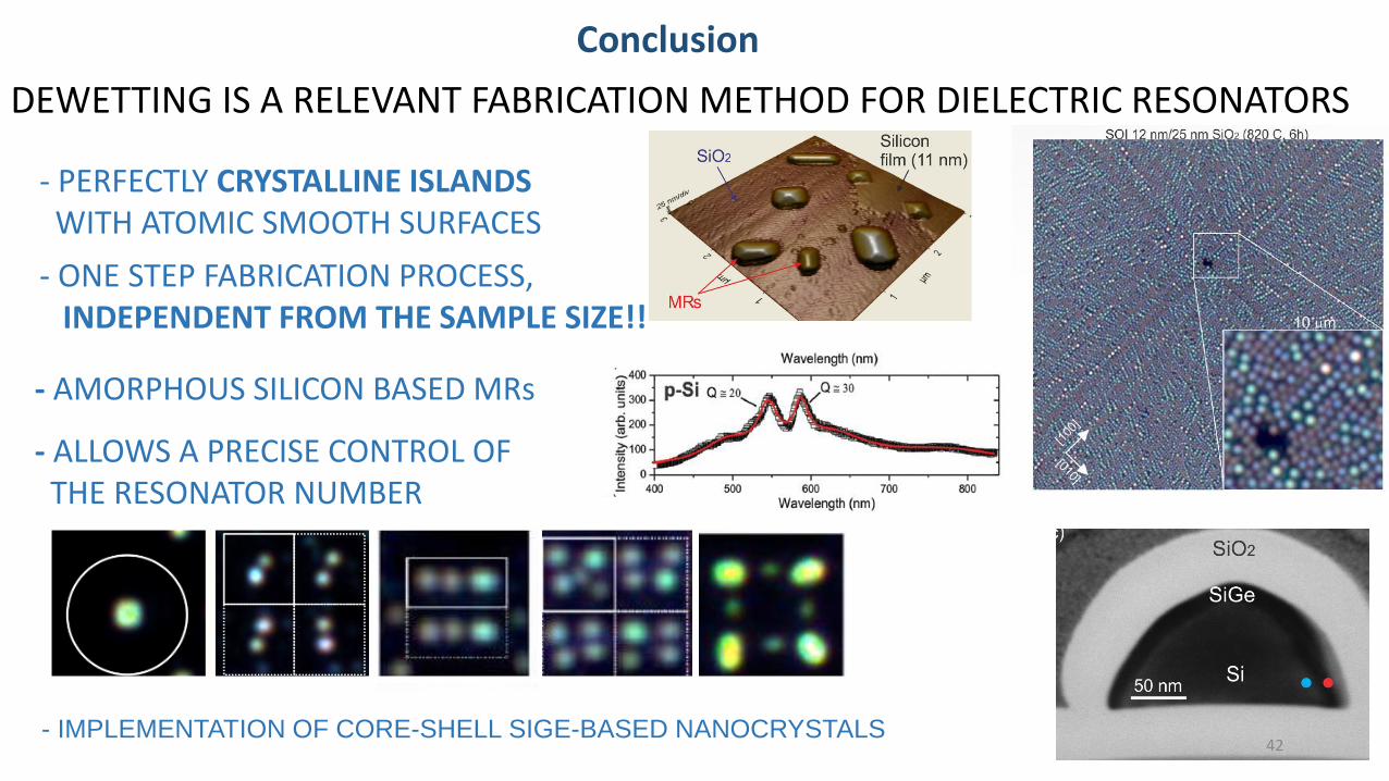
Conclusion
DEWETTING IS A RELEVANT FABRICATION METHOD FOR DIELECTRIC RESONATORS
- PERFECTLY CRYSTALLINE ISLANDSWITH ATOMIC SMOOTH SURFACES
- ONE STEP FABRICATION PROCESS, INDEPENDENT FROM THE SAMPLE SIZE!!
- ALLOWS A PRECISE CONTROL OF THE RESONATOR NUMBER
- IMPLEMENTATION OF CORE-SHELL SIGE-BASED NANOCRYSTALS
- AMORPHOUS SILICON BASED MRs
42
Perspectives
• Electric control of the resonant scattering
• Near field optical spectroscopy in order toinvestigate the distribution of the electricmode and magnetic mode inside NCs
• Theoretical model to explain the nucleationof the complex assemblies of MieResonators
• Optical characterization of SiGe core-shellnanostructures
• C-V characterization
43


![ABSTRACT of Doctoral Thesis - pavelstransky.cz€¦ · ABSTRACT of Doctoral Thesis ... The thesis is based particularly on published references [I, II, VII, VIII]. This abstract begins](https://static.fdocuments.fr/doc/165x107/5fbce8e8307fb30f38694377/abstract-of-doctoral-thesis-abstract-of-doctoral-thesis-the-thesis-is-based.jpg)