Thermal conductivity and mechanical properties of AlN ...
11
Thermal conductivity and mechanical properties of AlN-based thin films V. Moraes, H. Riedl, R. Rachbauer, S. Kolozsvári, M. Ikeda, L. Prochaska, S. Paschen, and P. H. Mayrhofer Citation: Journal of Applied Physics 119, 225304 (2016); doi: 10.1063/1.4953358 View online: http://dx.doi.org/10.1063/1.4953358 View Table of Contents: http://scitation.aip.org/content/aip/journal/jap/119/22?ver=pdfcov Published by the AIP Publishing Articles you may be interested in Substrate-dependent thermal conductivity of aluminum nitride thin-films processed at low temperature Appl. Phys. Lett. 105, 221905 (2014); 10.1063/1.4903220 Physical properties of Al x In1− x N thin film alloys sputtered at low temperature J. Appl. Phys. 116, 153509 (2014); 10.1063/1.4898565 Impact of the surface-near silicon substrate properties on the microstructure of sputter-deposited AlN thin films Appl. Phys. Lett. 101, 221602 (2012); 10.1063/1.4768951 Pulsed photothermal reflectance measurement of the thermal conductivity of sputtered aluminum nitride thin films J. Appl. Phys. 96, 4563 (2004); 10.1063/1.1785850 Thermal stability of InGaN multiple-quantum-well light-emitting diodes on an AlN/sapphire template J. Appl. Phys. 95, 3170 (2004); 10.1063/1.1646442 Reuse of AIP Publishing content is subject to the terms at: https://publishing.aip.org/authors/rights-and-permissions. Download to IP: 128.131.142.235 On: Wed, 29 Jun 2016 12:59:36
Transcript of Thermal conductivity and mechanical properties of AlN ...
Thermal conductivity and mechanical properties of AlN-based thin filmsV. Moraes, H. Riedl, R. Rachbauer, S. Kolozsvári, M. Ikeda, L. Prochaska, S. Paschen, and P. H. Mayrhofer Citation: Journal of Applied Physics 119, 225304 (2016); doi: 10.1063/1.4953358 View online: http://dx.doi.org/10.1063/1.4953358 View Table of Contents: http://scitation.aip.org/content/aip/journal/jap/119/22?ver=pdfcov Published by the AIP Publishing Articles you may be interested in Substrate-dependent thermal conductivity of aluminum nitride thin-films processed at low temperature Appl. Phys. Lett. 105, 221905 (2014); 10.1063/1.4903220 Physical properties of Al x In1− x N thin film alloys sputtered at low temperature J. Appl. Phys. 116, 153509 (2014); 10.1063/1.4898565 Impact of the surface-near silicon substrate properties on the microstructure of sputter-deposited AlN thin films Appl. Phys. Lett. 101, 221602 (2012); 10.1063/1.4768951 Pulsed photothermal reflectance measurement of the thermal conductivity of sputtered aluminum nitride thin films J. Appl. Phys. 96, 4563 (2004); 10.1063/1.1785850 Thermal stability of InGaN multiple-quantum-well light-emitting diodes on an AlN/sapphire template J. Appl. Phys. 95, 3170 (2004); 10.1063/1.1646442
Reuse of AIP Publishing content is subject to the terms at: https://publishing.aip.org/authors/rights-and-permissions. Download to IP: 128.131.142.235 On: Wed, 29 Jun
2016 12:59:36

Thermal conductivity and mechanical properties of AlN-based thin films
V. Moraes,1,a) H. Riedl,1 R. Rachbauer,2 S. Kolozsv�ari,3 M. Ikeda,4 L. Prochaska,4
S. Paschen,4 and P. H. Mayrhofer1,5
1Christian Doppler Laboratory for Application Oriented Coating Development at the Institute of MaterialsScience and Technology, TU Wien, A-1060 Wien, Austria2Oerlikon Balzers, Oerlikon Surface Solutions AG, LI-9496 Balzers, Liechtenstein3Plansee Composite Materials GmbH, D-86983 Lechbruck am See, Germany4Institute of Solid State Physics, TU Wien, A-1040 Wien, Austria5Institute of Materials Science and Technology, TU Wien, A-1060 Vienna, Austria
(Received 15 March 2016; accepted 24 May 2016; published online 10 June 2016)
While many research activities concentrate on mechanical properties and thermal stabilities of
protective thin films, only little is known about their thermal properties being essential for the
thermal management in various industrial applications. Based on the 3x-method, we show the
influence of Al and Cr on the temperature dependent thermal conductivity of single-phase cubic
structured TiN and single-phase wurtzite structured AlN thin films, respectively, and compare them
with the results obtained for CrN thin films. The dc sputtered AlN thin films revealed a highly c-axis
oriented growth for deposition temperatures of 250 to 700 �C. Their thermal conductivity was found
to increase strongly with the film thickness, indicating progressing crystallization of the interface
near amorphous regions during the sputtering process. For the 940 nm AlN film, we found a lower
boundary for the thermal conductivity of 55:3 W m�1 K�1. By the substitution of only 10 at. % Al
with Cr, j significantly reduces to �5:0 W m�1 K�1, although the single-phase wurtzite structure is
maintained. The single-phase face centered cubic TiN and Ti0.36Al0.64N thin films exhibit j values
of 3:1 W m�1 K�1 and 2:5 W m�1 K�1, respectively, at room temperature. Hence, also here, the sub-
stitutional alloying reduces the thermal conductivity, although at a significantly lower level. Single-
phase face centered cubic CrN thin films show j values of 3:6 W m�1 K�1. For all nitride based thin
films investigated, the thermal conductivity slightly increases with increasing temperature between
200 and 330 K. This rather unusual behavior is based on the high defect density (especially point
defects) within the thin films prepared by physical vapor deposition. Published by AIP Publishing.[http://dx.doi.org/10.1063/1.4953358]
I. INTRODUCTION
The rapidly growing development of nitride based thin
films has led to a great variety of applications. In addition to
the very important field of protective coatings for the machin-
ing and forming industry or protective coatings for aerospace
applications, nitrides are increasingly important not only for
their specific (semi-) conducting and piezoelectric properties
but also for their specific thermal properties.1 For example,
hexagonal closed packed (B4, wurtzite ZnS, abbreviated with
w-) aluminum nitride thin films, a representative of the III-V
semiconductors, have drawn great attention over the last deca-
des due to their extremely high thermal conductivity combined
with a rather low electrical conductivity (band gap of about
6 eV).2 The additional excellent thermal stability and high me-
chanical properties of AlN are extremely attractive combina-
tions for highly sophisticated applications, like functional thin
films that also need to withstand friction and wear.2,3 AlN is
also an ideal candidate for surface acoustic wave devices, due
to the outstanding optical and piezoelectric properties com-
bined with a high acoustic velocity of up to 6000 ms–1.4,5
Face centered cubic (B1, NaCl, abbreviated with c-) tita-
nium nitride and chromium nitride based coatings, which are
famous for their wear resistance, diffusion barrier abilities, and
tribological properties, are examples of nitrides with a rather
low thermal conductivity (j) with j � 4:8 W m–1 K–1.6,7
These material combinations are ideal for the application as
protective hard coatings in forming and tooling industry, lead-
ing to the great success of these coatings in these areas.
Moreover, TiN thin films are used in solar cells, as high tem-
perature diffusion barriers and Shottky or ohmic contact layers
in microelectronic devices.8 Ti1�xAlxN coatings, which are
favored in various machining operations, exhibit a pronounced
ability for self-adaption in mechanical as well as electrical and
thermal properties upon annealing treatments (or during expo-
sure to higher temperatures during application) because the
single-phase face centered cubic (c) structure decomposes
towards the stable constituents c-TiN and wurtzite structured
(w) AlN.9
The thermal conductivity of single-phase w-AlN (a sin-
gle crystal would have just one grain/grain size) strongly
depends on the oxygen content, grain size, and crystal orien-
tation, and can be as high as 320 W m–1 K–1.10 Especially,
the crystal structure of AlN (hexagonal wurtzite (B4), cubic
zinc blend (B3), or face centered cubic rock salt (B1) like
TiN and CrN) plays a major role in determining the thermal
conductivity due to the primarily responsible heat conduc-
tion mechanism, the phonons. Four requirements are neededa)[email protected]
0021-8979/2016/119(22)/225304/10/$30.00 Published by AIP Publishing.119, 225304-1
JOURNAL OF APPLIED PHYSICS 119, 225304 (2016)
Reuse of AIP Publishing content is subject to the terms at: https://publishing.aip.org/authors/rights-and-permissions. Download to IP: 128.131.142.235 On: Wed, 29 Jun
2016 12:59:36

to obtain a high thermal conductivity: low atomic mass,
strong bonding, simple crystal structure, and a low inhar-
monic behavior.11 Furthermore, various studies clearly show
that the growth techniques, the synthesis conditions, and the
substrates used have a strong influence on the microstructure,
the crystalline quality of the nitride coatings, and thus also
on the derived mechanical and thermal properties.12–14
Therefore, the reported values on the thermal conductivity of
AlN thin films cover a tremendously huge range from j� 5
to 200 W m–1 K–1.15–18
As the thermal conductivity is strongly influenced by the
crystal structure, we need to mention that especially the crys-
tal structure of various nitrides can be designed and modified
by knowledge-based alloying with various elements, please
see for example, the ab-initio as well as experimental studies
reported in Refs. 21 and 22.
The thermal conductivity can be obtained by several
measurement techniques,23 where the 3x-method overcomes
the difficulties of black body radiation. It can be extended
for measurements at different temperatures, and counts to
the most reliable and accurate techniques.24–26 Therefore,
this technique was the choice of investigation in our studies.
For a detailed study on the influence of crystal structure,
morphology, alloying effect, and deposition conditions on
the thermal conductivity (obtained by the 3x-method in the
temperature range 200 to 330 K) of nitride coatings, we used
the single-phase model systems: w-AlN, w-Al0.90Cr0.10N,
face centered cubic c-CrN, c-TiN, and c-Ti0.36Al0.64N.
II. EXPERIMENTAL
All AlN, Al1�xCrxN, CrN, TiN, and Ti1�xAlxN thin
films were prepared by reactive magnetron sputtering (AJA
Orion 5 laboratory-scaled PVD) using a mixed Ar/N2 glow
discharge at a working pressure of 0.4 Pa (both gases with
99.999% purity). Prior to the depositions, the 100-oriented Si
substrates (20� 7� 0:38 mm3; 10� 10� 0:38 mm3) were
ultrasonically pre-cleaned in acetone and ethanol, and dc
plasma-etched in a pure argon atmosphere at 6.0 Pa for
10 min. To minimize the effect of impurities, the deposition
chamber was always evacuated to a base pressure of �0.9
mPa. To guarantee for a uniform morphology, structure, and
chemical compositions of the coatings, the substrate-holder
(6 in. diameter) was rotated with a frequency of 1 Hz during
all depositions.
The aluminum nitride thin films are prepared by power-
ing the 3 in. aluminum target (99.99% purity) with
11 W cm�2 in dc mode using an Ar/N2 flow rate ratio of 1/9.
Eight different AlN thin films are prepared by varying the
substrate temperature (Tdep¼ 250, 400, 500, 600, 700, or
800 �C) and the bias potential (floating for all temperatures
and �75 V for Tdep¼ 250 and 500 �C) in order to analyse
their influences on the texture and thermal conductivity,
respectively. Additionally, the AlN coatings prepared at
Tdep¼ 250 and 500 �C (with floating and �75 V dc bias)
were grown with three different thicknesses between �190
and 1360 nm. Thus, 17 different AlN films were prepared
(for more details please see Table I).
The Al1�xCrxN, CrN, TiN, and Ti1�xAlxN coatings were
only prepared at Tdep¼ 500 �C. The Al0.90Cr0.10N coating,
exhibiting a thickness of 1180 nm, is prepared by simultane-
ous powering the 3 in. aluminum target with 11 W cm–2 and
the 2 in. chromium target with 2:5 W cm–2, and using an Ar/
N2 flow rate ratio of 1/9 with floating potential of the sub-
strates. CrN coatings are prepared with 12:1 W cm–2 dc
powering of the 2 in. chromium target (99.9% purity), an
Ar/N2 flow rate ratio of 4/6, and �50 V dc bias potential of
the substrates, leading to 1070 nm thickness. The TiN coat-
ing, of 580 nm thickness, is prepared by dc powering the
TABLE I. Deposition parameters and chemical composition of the thin films prepared by PVD.
Specimen Tdep (�C) Bias (V) Al (at. % Ti (at. %) Cr (at. %) N (at. %) Thickness (nm) Dep. rate (nm/min)
AlN 250 … … … … … 200 15.6
AlN 250 … … … … … 940 15.6
AlN 250 … … … … … 1320 15.6
AlN 250 �75 … … … … 220 15.5
AlN 250 �75 … … … … 490 15.5
AlN 250 �75 … … … … 910 15.6
AlN 500 … … … … … 190 16.0
AlN 500 … 44.91 … … 55.09 1050 16.0
AlN 500 … … … … … 1360 16.0
AlN 500 �75 … … … … 200 14.9
AlN 500 �75 … … … … 520 14.9
AlN 500 �75 43.31 … … 56.69 940 14.9
AlN 300 … … … … … 2190 18.3
AlN 400 … … … … … 2000 16.7
AlN 600 … … … … … 1400 11.7
AlN 700 … … … … … 1340 11.2
AlN 800 … … … … … 1030 8.6
Al1–xCrxN 500 … 44.64 … 4.91 50.45 1180 23.6
CrN 500 �50 … … 50.13 49.87 1070 7.6
TiN 500 … … 38.97 … 61.03 580 5.8
Ti1�xAlxN 500 �80 32.01 17.87 … 50.12 670 22.3
225304-2 Moraes et al. J. Appl. Phys. 119, 225304 (2016)
Reuse of AIP Publishing content is subject to the terms at: https://publishing.aip.org/authors/rights-and-permissions. Download to IP: 128.131.142.235 On: Wed, 29 Jun
2016 12:59:36
2 in. titanium target (99.9% purity) with 12:1 W cm–2 using
an Ar/N2 flow rate ratio of 8/2 and floating potential of the
substrates. The 670 nm thin Ti0.36Al0.64N film is prepared by
dc powering the 3 in. Ti0.33Al0.66 compound target (99.9%
purity) with 8:8 W cm–2 in an Ar/N2 gas mixture (Ar/N2
flow rate ratio of 7/3) and applying �80 V dc bias to the
substrates. All targets used are from Plansee Composite
Materials GmbH. The deposition parameters for all coatings
deposited are given in Table I.
The cross plane thermal conductivity of the thin films
was determined applying a differential 3x technique27 using
a home-built 3x setup. In detail, the thermal conductivity of
the thin films was determined by measuring two comparable
samples on identical substrates with different thicknesses.
For each 3x experiment, a narrow metal strip serves as both
the heater and the temperature sensor. This metal strip is
heated by an oscillating current at a circular frequency x,
which thus leads to a 2x temperature oscillation of the
heater, the sample, and the substrate. Due to the linear
temperature dependence of the metallic heater, the 2x tem-
perature oscillation translates to a 3x voltage oscillation,
which is detected using a lock-in amplifier (7265, Signal
Recovery). Prior to the thermal 3x voltage detection, the
first harmonic and all related higher harmonics are sub-
tracted from the signal using an active filter design based
on the technique suggested by Cahill et al.24,28 As long as
the thermal penetration depth within the substrate
���� 1q���� ¼
ffiffiffiffiffiffiD
2x
r; (1)
is large compared to the heater half width b and at least five
times smaller than the substrate thickness ts, the amplitude of
the temperature oscillation is given by24
DT ¼ P
lpj� 1
2ln 2xð Þ � 1
2ln
b2
D
� �þ ln 2ð Þ � i
p4
� �; (2)
where P/l is the line power density, D is the thermal diffusiv-
ity of the substrate, and i is the imaginary unit. In the case
that the thermal conductivity of the thin film jf is small com-
pared to the thermal conductivity of the substrate, the film
behaves as a simple thermal resistance and adds a frequency
independent offset to the temperature oscillation. Thus, by
measuring two comparable films with different thicknesses,
the thermal conductivity of the films27 can be determined
from
DTf ¼P
ljf
tf
2b; (3)
where DTf is the frequency independent offset to the temper-
ature oscillation and tf is the differential film thickness.
The required metal heaters on top of the thin films were
prepared by photolithography and sputtering. To avoid elec-
trical contact between the heater and the sample, each speci-
men, except the AlN thin films, was additionally covered
with a �300 nm thin AlN layer prior to the heater deposition.
Due to the chemical etching of the insulating AlN layers, the
less labor-intensive lift off method with KOH based develop-
ers29–31 could not be used to produce the heater structures.
Instead, the ion etching technique had to be applied.
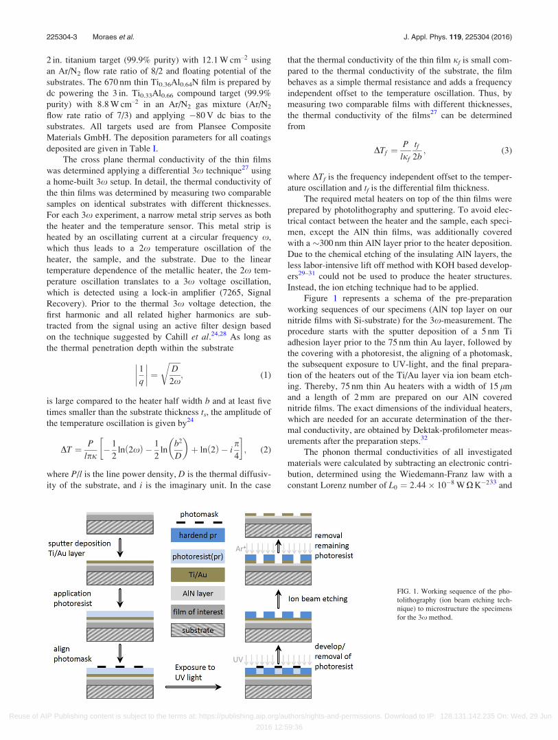
Figure 1 represents a schema of the pre-preparation
working sequences of our specimens (AlN top layer on our
nitride films with Si-substrate) for the 3x-measurement. The
procedure starts with the sputter deposition of a 5 nm Ti
adhesion layer prior to the 75 nm thin Au layer, followed by
the covering with a photoresist, the aligning of a photomask,
the subsequent exposure to UV-light, and the final prepara-
tion of the heaters out of the Ti/Au layer via ion beam etch-
ing. Thereby, 75 nm thin Au heaters with a width of 15 lm
and a length of 2 mm are prepared on our AlN covered
nitride films. The exact dimensions of the individual heaters,
which are needed for an accurate determination of the ther-
mal conductivity, are obtained by Dektak-profilometer meas-
urements after the preparation steps.32
The phonon thermal conductivities of all investigated
materials were calculated by subtracting an electronic contri-
bution, determined using the Wiedemann-Franz law with a
constant Lorenz number of L0 ¼ 2:44� 10�8 W X K�233 and
FIG. 1. Working sequence of the pho-
tolithography (ion beam etching tech-
nique) to microstructure the specimens
for the 3x method.
225304-3 Moraes et al. J. Appl. Phys. 119, 225304 (2016)
Reuse of AIP Publishing content is subject to the terms at: https://publishing.aip.org/authors/rights-and-permissions. Download to IP: 128.131.142.235 On: Wed, 29 Jun
2016 12:59:36
electrical resistivity data measured using the Van-der-Pauw
method.34
The bi-axial stresses within our thin films are calculated
via the modified stoney equation using the curvature of the
coated Si substrates, obtained by a Nanovea PS50 profilome-
ter.35 By scanning electron microscopy (SEM, FEI Quanta
200 equipped with a field emission gun) and transmission
electron microscopy (TEM, FEI TECNAI F20) of sample
cross-sections, the growth morphology of our films is studied.
Chemical compositions of our films are obtained by energy
dispersive X-ray spectroscopy (EDS). Due to element-specific
absorption, different accelerating voltages of 10, 15, and
20 kV were used.
The structure and crystalline phases of our thin films are
analyzed by X-ray diffraction (XRD) in gracing incidence
mode (Empyrean Panalytical diffractometer) with a Cu-Ka
(k¼ 1.54 A) radiation source. Our coatings are also charac-
terized for their mechanical properties (hardness (H) and
indentation modulus (E)), which are evaluated throughout
the loading and unloading segment of the indentation curves
(using a UMIS Nanoindenter equipped with a Berkovich tip)
according to the Oliver and Pharr method.36
III. RESULTS AND DISCUSSION
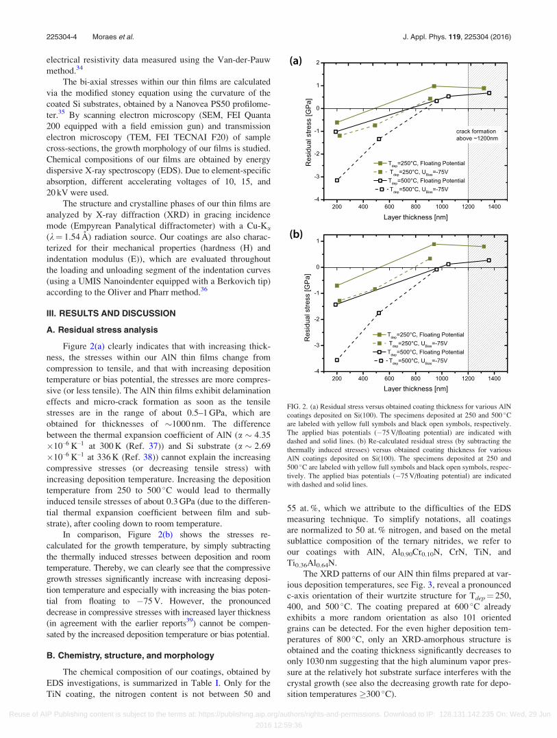
A. Residual stress analysis
Figure 2(a) clearly indicates that with increasing thick-
ness, the stresses within our AlN thin films change from
compression to tensile, and that with increasing deposition
temperature or bias potential, the stresses are more compres-
sive (or less tensile). The AlN thin films exhibit delamination
effects and micro-crack formation as soon as the tensile
stresses are in the range of about 0.5–1 GPa, which are
obtained for thicknesses of �1000 nm. The difference
between the thermal expansion coefficient of AlN (a � 4:35
�10–6 K–1 at 300 K (Ref. 37)) and Si substrate (a � 2:69
�10–6 K–1 at 336 K (Ref. 38)) cannot explain the increasing
compressive stresses (or decreasing tensile stress) with
increasing deposition temperature. Increasing the deposition
temperature from 250 to 500 �C would lead to thermally
induced tensile stresses of about 0.3 GPa (due to the differen-
tial thermal expansion coefficient between film and sub-
strate), after cooling down to room temperature.
In comparison, Figure 2(b) shows the stresses re-
calculated for the growth temperature, by simply subtracting
the thermally induced stresses between deposition and room
temperature. Thereby, we can clearly see that the compressive
growth stresses significantly increase with increasing deposi-
tion temperature and especially with increasing the bias poten-
tial from floating to �75 V. However, the pronounced
decrease in compressive stresses with increased layer thickness
(in agreement with the earlier reports39) cannot be compen-
sated by the increased deposition temperature or bias potential.
B. Chemistry, structure, and morphology
The chemical composition of our coatings, obtained by
EDS investigations, is summarized in Table I. Only for the
TiN coating, the nitrogen content is not between 50 and
55 at. %, which we attribute to the difficulties of the EDS
measuring technique. To simplify notations, all coatings
are normalized to 50 at. % nitrogen, and based on the metal
sublattice composition of the ternary nitrides, we refer to
our coatings with AlN, Al0.90Cr0.10N, CrN, TiN, and
Ti0.36Al0.64N.
The XRD patterns of our AlN thin films prepared at var-
ious deposition temperatures, see Fig. 3, reveal a pronounced
c-axis orientation of their wurtzite structure for Tdep¼ 250,
400, and 500 �C. The coating prepared at 600 �C already
exhibits a more random orientation as also 101 oriented
grains can be detected. For the even higher deposition tem-
peratures of 800 �C, only an XRD-amorphous structure is
obtained and the coating thickness significantly decreases to
only 1030 nm suggesting that the high aluminum vapor pres-
sure at the relatively hot substrate surface interferes with the
crystal growth (see also the decreasing growth rate for depo-
sition temperatures �300 �C).
FIG. 2. (a) Residual stress versus obtained coating thickness for various AlN
coatings deposited on Si(100). The specimens deposited at 250 and 500 �Care labeled with yellow full symbols and black open symbols, respectively.
The applied bias potentials (�75 V/floating potential) are indicated with
dashed and solid lines. (b) Re-calculated residual stress (by subtracting the
thermally induced stresses) versus obtained coating thickness for various
AlN coatings deposited on Si(100). The specimens deposited at 250 and
500 �C are labeled with yellow full symbols and black open symbols, respec-
tively. The applied bias potentials (�75 V/floating potential) are indicated
with dashed and solid lines.
225304-4 Moraes et al. J. Appl. Phys. 119, 225304 (2016)
Reuse of AIP Publishing content is subject to the terms at: https://publishing.aip.org/authors/rights-and-permissions. Download to IP: 128.131.142.235 On: Wed, 29 Jun
2016 12:59:36
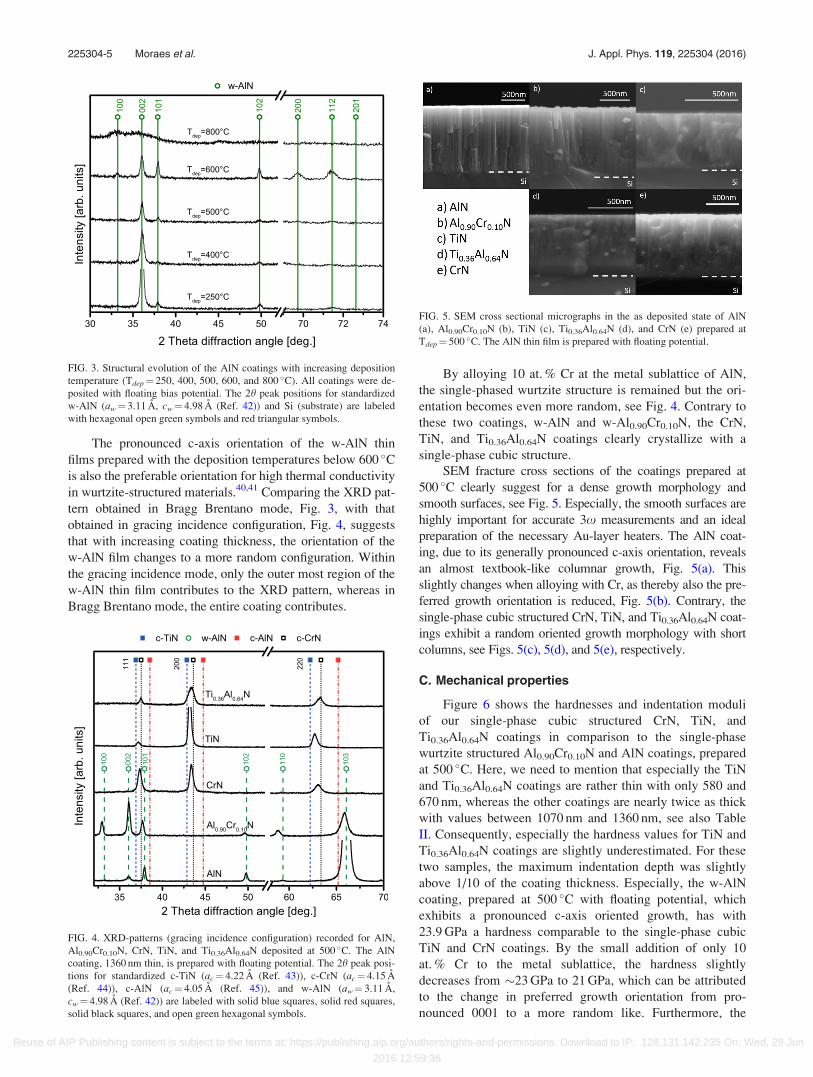
The pronounced c-axis orientation of the w-AlN thin
films prepared with the deposition temperatures below 600 �Cis also the preferable orientation for high thermal conductivity
in wurtzite-structured materials.40,41 Comparing the XRD pat-
tern obtained in Bragg Brentano mode, Fig. 3, with that
obtained in gracing incidence configuration, Fig. 4, suggests
that with increasing coating thickness, the orientation of the
w-AlN film changes to a more random configuration. Within
the gracing incidence mode, only the outer most region of the
w-AlN thin film contributes to the XRD pattern, whereas in
Bragg Brentano mode, the entire coating contributes.
By alloying 10 at. % Cr at the metal sublattice of AlN,
the single-phased wurtzite structure is remained but the ori-
entation becomes even more random, see Fig. 4. Contrary to
these two coatings, w-AlN and w-Al0.90Cr0.10N, the CrN,
TiN, and Ti0.36Al0.64N coatings clearly crystallize with a
single-phase cubic structure.
SEM fracture cross sections of the coatings prepared at
500 �C clearly suggest for a dense growth morphology and
smooth surfaces, see Fig. 5. Especially, the smooth surfaces are
highly important for accurate 3x measurements and an ideal
preparation of the necessary Au-layer heaters. The AlN coat-
ing, due to its generally pronounced c-axis orientation, reveals
an almost textbook-like columnar growth, Fig. 5(a). This
slightly changes when alloying with Cr, as thereby also the pre-
ferred growth orientation is reduced, Fig. 5(b). Contrary, the
single-phase cubic structured CrN, TiN, and Ti0.36Al0.64N coat-
ings exhibit a random oriented growth morphology with short
columns, see Figs. 5(c), 5(d), and 5(e), respectively.
C. Mechanical properties
Figure 6 shows the hardnesses and indentation moduli
of our single-phase cubic structured CrN, TiN, and
Ti0.36Al0.64N coatings in comparison to the single-phase
wurtzite structured Al0.90Cr0.10N and AlN coatings, prepared
at 500 �C. Here, we need to mention that especially the TiN
and Ti0.36Al0.64N coatings are rather thin with only 580 and
670 nm, whereas the other coatings are nearly twice as thick
with values between 1070 nm and 1360 nm, see also Table
II. Consequently, especially the hardness values for TiN and
Ti0.36Al0.64N coatings are slightly underestimated. For these
two samples, the maximum indentation depth was slightly
above 1/10 of the coating thickness. Especially, the w-AlN
coating, prepared at 500 �C with floating potential, which
exhibits a pronounced c-axis oriented growth, has with
23.9 GPa a hardness comparable to the single-phase cubic
TiN and CrN coatings. By the small addition of only 10
at. % Cr to the metal sublattice, the hardness slightly
decreases from �23 GPa to 21 GPa, which can be attributed
to the change in preferred growth orientation from pro-
nounced 0001 to a more random like. Furthermore, the
FIG. 3. Structural evolution of the AlN coatings with increasing deposition
temperature (Tdep¼ 250, 400, 500, 600, and 800 �C). All coatings were de-
posited with floating bias potential. The 2h peak positions for standardized
w-AlN (aw¼ 3.11 A, cw¼ 4.98 A (Ref. 42)) and Si (substrate) are labeled
with hexagonal open green symbols and red triangular symbols.
FIG. 4. XRD-patterns (gracing incidence configuration) recorded for AlN,
Al0.90Cr0.10N, CrN, TiN, and Ti0.36Al0.64N deposited at 500 �C. The AlN
coating, 1360 nm thin, is prepared with floating potential. The 2h peak posi-
tions for standardized c-TiN (ac¼ 4.22 A (Ref. 43)), c-CrN (ac¼ 4.15 A
(Ref. 44)), c-AlN (ac¼ 4.05 A (Ref. 45)), and w-AlN (aw¼ 3.11 A,
cw¼ 4.98 A (Ref. 42)) are labeled with solid blue squares, solid red squares,
solid black squares, and open green hexagonal symbols.
FIG. 5. SEM cross sectional micrographs in the as deposited state of AlN
(a), Al0.90Cr0.10N (b), TiN (c), Ti0.36Al0.64N (d), and CrN (e) prepared at
Tdep¼ 500 �C. The AlN thin film is prepared with floating potential.
225304-5 Moraes et al. J. Appl. Phys. 119, 225304 (2016)
Reuse of AIP Publishing content is subject to the terms at: https://publishing.aip.org/authors/rights-and-permissions. Download to IP: 128.131.142.235 On: Wed, 29 Jun
2016 12:59:36
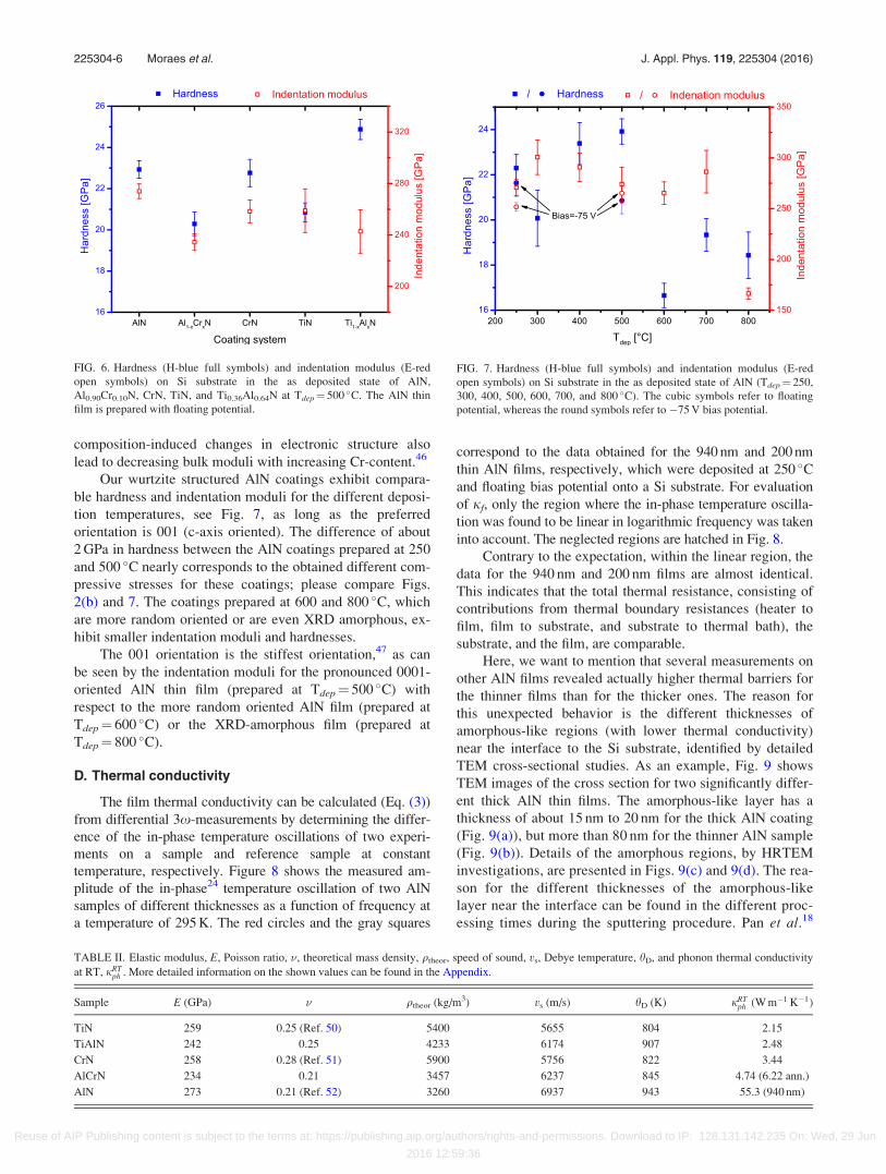
composition-induced changes in electronic structure also
lead to decreasing bulk moduli with increasing Cr-content.46
Our wurtzite structured AlN coatings exhibit compara-
ble hardness and indentation moduli for the different deposi-
tion temperatures, see Fig. 7, as long as the preferred
orientation is 001 (c-axis oriented). The difference of about
2 GPa in hardness between the AlN coatings prepared at 250
and 500 �C nearly corresponds to the obtained different com-
pressive stresses for these coatings; please compare Figs.
2(b) and 7. The coatings prepared at 600 and 800 �C, which
are more random oriented or are even XRD amorphous, ex-
hibit smaller indentation moduli and hardnesses.
The 001 orientation is the stiffest orientation,47 as can
be seen by the indentation moduli for the pronounced 0001-
oriented AlN thin film (prepared at Tdep¼ 500 �C) with
respect to the more random oriented AlN film (prepared at
Tdep¼ 600 �C) or the XRD-amorphous film (prepared at
Tdep¼ 800 �C).
D. Thermal conductivity
The film thermal conductivity can be calculated (Eq. (3))
from differential 3x-measurements by determining the differ-
ence of the in-phase temperature oscillations of two experi-
ments on a sample and reference sample at constant
temperature, respectively. Figure 8 shows the measured am-
plitude of the in-phase24 temperature oscillation of two AlN
samples of different thicknesses as a function of frequency at
a temperature of 295 K. The red circles and the gray squares
correspond to the data obtained for the 940 nm and 200 nm
thin AlN films, respectively, which were deposited at 250 �Cand floating bias potential onto a Si substrate. For evaluation
of jf, only the region where the in-phase temperature oscilla-
tion was found to be linear in logarithmic frequency was taken
into account. The neglected regions are hatched in Fig. 8.
Contrary to the expectation, within the linear region, the
data for the 940 nm and 200 nm films are almost identical.
This indicates that the total thermal resistance, consisting of
contributions from thermal boundary resistances (heater to
film, film to substrate, and substrate to thermal bath), the
substrate, and the film, are comparable.
Here, we want to mention that several measurements on
other AlN films revealed actually higher thermal barriers for
the thinner films than for the thicker ones. The reason for
this unexpected behavior is the different thicknesses of
amorphous-like regions (with lower thermal conductivity)
near the interface to the Si substrate, identified by detailed
TEM cross-sectional studies. As an example, Fig. 9 shows
TEM images of the cross section for two significantly differ-
ent thick AlN thin films. The amorphous-like layer has a
thickness of about 15 nm to 20 nm for the thick AlN coating
(Fig. 9(a)), but more than 80 nm for the thinner AlN sample
(Fig. 9(b)). Details of the amorphous regions, by HRTEM
investigations, are presented in Figs. 9(c) and 9(d). The rea-
son for the different thicknesses of the amorphous-like
layer near the interface can be found in the different proc-
essing times during the sputtering procedure. Pan et al.18
TABLE II. Elastic modulus, E, Poisson ratio, �, theoretical mass density, qtheor, speed of sound, vs, Debye temperature, hD, and phonon thermal conductivity
at RT, jRTph . More detailed information on the shown values can be found in the Appendix.
Sample E (GPa) � qtheor (kg/m3) vs (m/s) hD (K) jRTph (W m�1 K�1)
TiN 259 0.25 (Ref. 50) 5400 5655 804 2.15
TiAlN 242 0.25 4233 6174 907 2.48
CrN 258 0.28 (Ref. 51) 5900 5756 822 3.44
AlCrN 234 0.21 3457 6237 845 4.74 (6.22 ann.)
AlN 273 0.21 (Ref. 52) 3260 6937 943 55.3 (940 nm)
FIG. 6. Hardness (H-blue full symbols) and indentation modulus (E-red
open symbols) on Si substrate in the as deposited state of AlN,
Al0.90Cr0.10N, CrN, TiN, and Ti0.36Al0.64N at Tdep¼ 500 �C. The AlN thin
film is prepared with floating potential.
FIG. 7. Hardness (H-blue full symbols) and indentation modulus (E-red
open symbols) on Si substrate in the as deposited state of AlN (Tdep¼ 250,
300, 400, 500, 600, 700, and 800 �C). The cubic symbols refer to floating
potential, whereas the round symbols refer to �75 V bias potential.
225304-6 Moraes et al. J. Appl. Phys. 119, 225304 (2016)
Reuse of AIP Publishing content is subject to the terms at: https://publishing.aip.org/authors/rights-and-permissions. Download to IP: 128.131.142.235 On: Wed, 29 Jun
2016 12:59:36
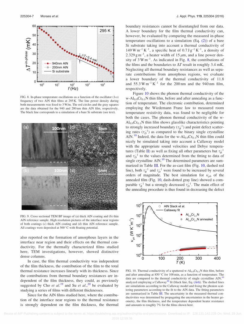
also reported on the formation of amorphous layers in the
interface near region and their effects on the thermal con-
ductivity. For the thermally characterized films studied
here, TEM investigations, however, showed distinctive
dense columns.
In case, the film thermal conductivity was independent
of the film thickness, the contribution of the film to the total
thermal resistance increases linearly with its thickness. Since
the contributions from thermal boundary resistances are in-
dependent of the film thickness, they could, as previously
suggested by Cho et al.19 and Su et al.,20 be evaluated by
studying a series of films with different thicknesses.
Since for the AlN films studied here, where the contribu-
tion of the interface near regions to the thermal resistance
is strongly dependent on the film thickness, the thermal
boundary resistances cannot be disentangled from our data.
A lower boundary for the film thermal conductivity can,
however, be evaluated by comparing the measured in-phase
temperature oscillations to a simulation (Eq. (2)) of a bare
Si substrate taking into account a thermal conductivity of
149 W m–1 K–1, a specific heat of 0:7 J g–1 K–1, a density of
2:329 g m–3, a heater width of 15 lm, and a line power den-
sity of 3 W m–1. As indicated in Fig. 8, the contributions of
the films and the boundaries to DT result in roughly 3.4 mK.
Neglecting all thermal boundary resistances as well as sepa-
rate contributions from amorphous regions, we evaluate
a lower boundary of the thermal conductivity of 11.8
and 55:3 W m–1 K–1 for the 200 nm and the 940 nm film,
respectively.
Figure 10 shows the phonon thermal conductivity of the
w-Al0.9Cr0.1N thin film, before and after annealing as a func-
tion of temperature. The electronic contribution, determined
employing the Wiedemann Franz law to measured room
temperature resistivity data, was found to be negligible for
both the cases. The phonon thermal conductivity of the w-
Al0.9Cr0.1N thin film shows glasslike characteristics pointing
to strongly increased boundary (s�1B ) and point defect scatter-
ing rates (s�1D ) as compared to the binary single crystalline
AlN.10 Indeed, the data for the w-Al0.9Cr0.1N thin film could
nicely be simulated taking into account a Callaway model
with the appropriate sound velocities and Debye tempera-
tures (Table II) as well as fixing all other parameters but s�1B
and s�1D to the values determined from the fitting to data of
single crystalline AlN.10 The determined parameters are sum-
marized in Table III. For the as-cast film (Fig. 10, dashed red
line), both s�1B and s�1
D were found to be increased by several
orders of magnitude. The best simulation for jph of the
annealed film (Fig. 10, dash-dotted gray line) showed a com-
parable s�1B but a strongly decreased s�1
D . The main effect of
the annealing procedure is thus found in decreasing the defect
FIG. 8. In-phase temperature oscillations as a function of the oscillator (1x)
frequency of two AlN thin films at 295 K. The line power density during
both measurements was fixed to 3 W/m. The red circles and the gray squares
are the data obtained for the 940 and 200 nm thin AlN film, respectively.
The black line corresponds to a simulation of a bare Si substrate (see text).
FIG. 9. Cross sectional TEM BF image of (a) thick AlN coating and (b) thin
AlN reference sample. High resolution pictures of the interface near regions
of both coatings (c) thick AlN coating and (d) thin AlN reference sample.
All coatings were deposited at 500 �C with floating potential.
FIG. 10. Thermal conductivity of a sputtered w-Al0.9Cr0.1N thin film, before
and after annealing at 850 �C for 100 min, as a function of temperature. The
data are compared to the thermal conductivity of single crystalline AlN,10
analyzed employing a Callaway49 fit (black line, Eq. (A4)). The dashed lines
are simulations according to the Callaway model and fixing the phonon scat-
tering parameters according to the fit to the AlN data. The fitting parameters
are summarized in Table III. The uncertainty in the measured thermal con-
ductivities was determined by propagating the uncertainties in the heater ge-
ometry, the film thickness, and the temperature dependent heater resistance
and amounts to roughly 7% for the films shown here.
225304-7 Moraes et al. J. Appl. Phys. 119, 225304 (2016)
Reuse of AIP Publishing content is subject to the terms at: https://publishing.aip.org/authors/rights-and-permissions. Download to IP: 128.131.142.235 On: Wed, 29 Jun
2016 12:59:36
concentration. The severe differences in the phonon disper-
sion of w-AlN28 and w-CrN48 indicate a strong dependence of
the phononic properties of Al1�xCrxN on the Cr-content, x.
To the first approximation, these effects were included to our
simulations by fixing the Debye temperature and the speed of
sound to the values determined from the indentation experi-
ments (Table II). However, quantitative statements cannot be
drawn from the employed Callaway analysis.
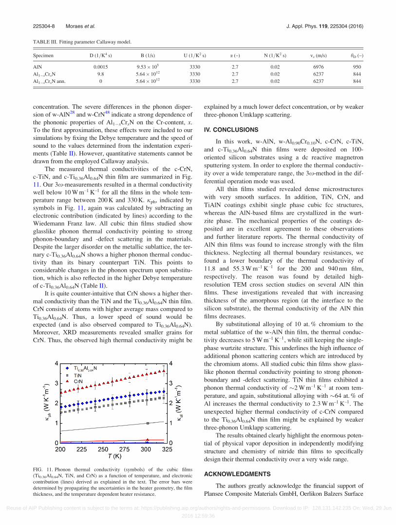
The measured thermal conductivities of the c-CrN,
c-TiN, and c-Ti0.36Al0.64N thin film are summarized in Fig.
11. Our 3x-measurements resulted in a thermal conductivity
well below 10 W m–1 K–1 for all the films in the whole tem-
perature range between 200 K and 330 K. jph, indicated by
symbols in Fig. 11, again was calculated by subtracting an
electronic contribution (indicated by lines) according to the
Wiedemann Franz law. All cubic thin films studied show
glasslike phonon thermal conductivity pointing to strong
phonon-boundary and -defect scattering in the materials.
Despite the larger disorder on the metallic sublattice, the ter-
nary c-Ti0.36Al0.64N shows a higher phonon thermal conduc-
tivity than its binary counterpart TiN. This points to
considerable changes in the phonon spectrum upon substitu-
tion, which is also reflected in the higher Debye temperature
of c-Ti0.36Al0.64N (Table II).
It is quite counter-intuitive that CrN shows a higher ther-
mal conductivity than the TiN and the Ti0.36Al0.64N thin film.
CrN consists of atoms with higher average mass compared to
Ti0.36Al0.64N. Thus, a lower speed of sound would be
expected (and is also observed compared to Ti0.36Al0.64N).
Moreover, XRD measurements revealed smaller grains for
CrN. Thus, the observed high thermal conductivity might be
explained by a much lower defect concentration, or by weaker
three-phonon Umklapp scattering.
IV. CONCLUSIONS
In this work, w-AlN, w-Al0.90Cr0.10N, c-CrN, c-TiN,
and c-Ti0.36Al0.64N thin films were deposited on 100-
oriented silicon substrates using a dc reactive magnetron
sputtering system. In order to explore the thermal conductiv-
ity over a wide temperature range, the 3x-method in the dif-
ferential operation mode was used.
All thin films studied revealed dense microstructures
with very smooth surfaces. In addition, TiN, CrN, and
TiAlN coatings exhibit single phase cubic fcc structures,
whereas the AlN-based films are crystallized in the wurt-
zite phase. The mechanical properties of the coatings de-
posited are in excellent agreement to these observations
and further literature reports. The thermal conductivity of
AlN thin films was found to increase strongly with the film
thickness. Neglecting all thermal boundary resistances, we
found a lower boundary of the thermal conductivity of
11.8 and 55:3 W m–1 K–1 for the 200 and 940 nm film,
respectively. The reason was found by detailed high-
resolution TEM cross section studies on several AlN thin
films. These investigations revealed that with increasing
thickness of the amorphous region (at the interface to the
silicon substrate), the thermal conductivity of the AlN thin
films decreases.
By substitutional alloying of 10 at. % chromium to the
metal sublattice of the w-AlN thin film, the thermal conduc-
tivity decreases to 5 W m–1 K–1, while still keeping the single-
phase wurtzite structure. This underlines the high influence of
additional phonon scattering centers which are introduced by
the chromium atoms. All studied cubic thin films show glass-
like phonon thermal conductivity pointing to strong phonon-
boundary and -defect scattering. TiN thin films exhibited a
phonon thermal conductivity of �2 W m–1 K–1 at room tem-
perature, and again, substitutional alloying with �64 at. % of
Al increases the thermal conductivity to 2:3 W m–1 K–1. The
unexpected higher thermal conductivity of c-CrN compared
to the Ti0.36Al0.64N thin film might be explained by weaker
three-phonon Umklapp scattering.
The results obtained clearly highlight the enormous poten-
tial of physical vapor deposition in independently modifying
structure and chemistry of nitride thin films to specifically
design their thermal conductivity over a very wide range.
ACKNOWLEDGMENTS
The authors greatly acknowledge the financial support of
Plansee Composite Materials GmbH, Oerlikon Balzers Surface
TABLE III. Fitting parameter Callaway model.
Specimen D (1=K4 s) B (1/s) U (1=K2 s) a (–) N (1=K2 s) vs (m/s) hD (–)
AlN 0.0015 9.53� 105 3330 2.7 0.02 6976 950
Al1�xCrxN 9.8 5.64� 1012 3330 2.7 0.02 6237 844
Al1�xCrxN ann. 0 5.64� 1012 3330 2.7 0.02 6237 844
FIG. 11. Phonon thermal conductivity (symbols) of the cubic films
(Ti0.36Al0.64N, TiN, and CrN) as a function of temperature, and electronic
contribution (lines) derived as explained in the text. The error bars were
determined by propagating the uncertainties in the heater geometry, the film
thickness, and the temperature dependent heater resistance.
225304-8 Moraes et al. J. Appl. Phys. 119, 225304 (2016)
Reuse of AIP Publishing content is subject to the terms at: https://publishing.aip.org/authors/rights-and-permissions. Download to IP: 128.131.142.235 On: Wed, 29 Jun
2016 12:59:36
Solutions AG, and the Christian Doppler Gesellschaft within the
framework of the Christian Doppler Laboratory for Application
Oriented Coating Development. M.I., L.P., and S.P.
acknowledge financial support from the Austrian Science Fund
(FWF W1243) and the Deutsche Forschungsgemeinschaft
(DFG SPP 1386). SEM investigations were carried out using
facilities at the Vienna University of Technology, Austria.
Thanks are also due to the X-ray center (XRC) of Vienna
University of Technology, Austria.
APPENDIX: CALLAWAY FITTING PARAMETERS
B ¼ffiffiffiffiffiffiffiffiffiffiffiffiffiffiffiffiffi
E
6� 3 � �
r; (A1)
vs ¼ffiffiffiB
q
s; (A2)
hD ¼ �hvs
kB
6p2 N
V
� �13
: (A3)
Bulk modulus, B, was calculated, using the elastic mod-
ulus, E, gained from the indentation experiments and litera-
ture data for the Poisson ratio �. By applying Eq. (A2) for
the speed of sound, the theoretical density q (using lattice
parameters obtained from the XRD measurements) was cal-
culated. Combining Eqs. (A1) and (A2), the debye tempera-
ture hD can be calculated.
jph ¼k4
B � T3
2 � p2 � vs � �h3�ðHD
T
0
s � x4 � ex
ex � 1ð Þ2� dxþ I2
I1
" #; with
I1 ¼ðHD
T
0
ssN
� x4 � ex
ex � 1ð Þ2� dx;
I2 ¼ðHD
T
0
1
sN
� 1� ssN
� �� x4 � ex
ex � 1ð Þ2� dx;
s�1 ¼ s�1N þ s�1
D þ s�1B þ s�1
U þ s�1ph�el:
(A4)
Normal processes are usually taken into account by
s�1N ¼ NxaTb; (A5)
where a and b are typically set to 2 and 3 for group III-V
materials. Defect scattering can be taken into account by
Rayleigh scattering53
s�1D ¼ D � x4; (A6)
and boundary scattering by a frequency independent scatter-
ing rate53
s�1B ¼ B: (A7)
Slack and Galginaitis.54 suggested an Umklapp scattering
rate taken into account by
s�1U ¼ UxcTde�
hDaT : (A8)
For c¼ 2, d¼ 1, and T � hD; s�1U becomes
s�1U / x2 � T: (A9)
This behavior was earlier published by Klemens.55
1P. M. Mayrhofer, C. Eisenmenger-Sittner, M. St€oger-Pollach, H. Euchner,
A. Bittner, and U. Schmid, J. Appl. Phys. 115, 193505 (2014).2S. Strite, J. Vac. Sci. Technol. B: Microelectron. Nanom. Struct. 10, 1237
(1992).3P. H. Mayrhofer, C. Mitterer, L. Hultman, and H. Clemens, Prog. Mater.
Sci. 51, 1032 (2006).4M. El Hakiki, O. Elmazria, M. Assouar, V. Mortet, A. Talbi, and F. Sarry,
Ultrasonics 1, 195 (2004).5H. Loebl, C. Metzmacher, R. Milsom, P. Lok, F. van Straten, and A.
Tuinhout, J. Electroceram. 12, 109 (2004).6J. Martan and P. Bene�s, Thermochim. Acta 539, 51 (2012).7P. H. M. B€ottger, L. Braginsky, V. Shklover, E. Lewin, J. Patscheider, D.
G. Cahill, and M. Sobiech, J. Appl. Phys. 116, 013507 (2014).8A. A. Irudayaraj, R. Srinivasan, P. Kuppusami, E. Mohandas, S.
Kalainathan, and K. Ramachandran, J. Mater. Sci. 43, 1114 (2008).9R. Rachbauer, S. Massl, E. Stergar, D. Holec, D. Kiener, J. Keckes, J.
Patscheider, M. Stiefel, H. Leitner, and P. H. Mayrhofer, J. Appl. Phys.
110, 023515 (2011).10G. A. Slack, R. Tanzilli, R. Pohl, and J. Vandersande, J. Phys. Chem.
Solids 48, 641 (1987).11G. Slack, J. Phys. Chem. Solids 34, 321–335 (1972).12C. C. Wang, C. J. Lu, M. H. Shiao, and F. S. Shieu, J. Vac. Sci. Technol., A
23, 621 (2005).13T. Aubert, M. B. Assouar, O. Legrani, O. Elmazria, C. Tiusan, and S.
Robert, J. Vac. Sci. Technol., A 29, 021010 (2011).14A. Khanna and D. G. Bhat, J. Vac. Sci. Technol., A 25, 557 (2007).15B. E. Belkerk, A. Soussou, M. Carette, M. A. Djouadi, and Y. Scudeller,
Appl. Phys. Lett. 101, 151908 (2012).16M.-H. Park and S.-H. Kim, Mater. Sci. Semicond. Process. 15, 6 (2012).17B. E. Belkerk, S. Bensalem, A. Soussou, M. Carette, H. A. Brithen, M. A.
Djouadi, and Y. Scudeller, Appl. Phys. Lett. 105, 221905 (2014).18T. S. Pan, Y. Zhang, J. Huang, B. Zeng, D. H. Hong, S. L. Wang, H. Z.
Zeng, M. Gao, W. Huang, and Y. Lin, J. Appl. Phys. 112, 044905 (2012).19J. Cho, Y. Li, W. E. Hoke, D. H. Altman, M. Ashegi, and K. E. Goodson,
Phys. Rev. B 89, 115301 (2014).20Z. Su, J. P. Freedman, J. H. Leach, E. A. Preble, R. F. Davis, and J. A.
Malen, J. Appl. Phys. 113, 213502 (2013).21F. Rovere and P. H. Mayrhofer, J. Vac. Sci. Technol., A 25, 1336 (2007).22D. Holec, L. Zhou, R. Rachbauer, and P. H. Mayrhofer, J. Appl. Phys.
113, 113510 (2013).23J. E. Graebner and H. Altmann, Diamond Relat. Mater. 7, 1589 (1998).24D. G. Cahill, Rev. Sci. Instrum. 61, 802 (1990).25T. Borca-Tasciuc, A. R. Kumar, and G. Chen, Rev. Sci. Instrum. 72, 2139
(2001).26M. Ikeda, Ph.D. thesis, TU Wien, 2015.27D. G. Cahill, M. Katiyar, and J. R. Abelson, Phys. Rev. B 50, 6077–6081
(1994).28V. Yu. Davydov, Yu. E. Kitaev, I. N. Goncharuk, A. N. Smirnov, J. Graul,
O. Semichinova, D. Uffmann, M. B. Smirnov, A. P. Mirgorodsky, and R.
A. Evarestov, Phys. Rev. B 58, 12899–12907 (1998).29H. Wang and M. Sen, Int. J. Heat Mass Transfer 52, 2102 (2009).30D. Zhuang and J. H. Edgar, Mater. Sci. Eng., R 48, 1 (2005).31G. R. Kline and K. M. Lakin, Appl. Phys. Lett. 43, 750 (1983).32Dektak 150 Profilometer Instructions.33G. S. Kumar, G. Prasad, and R. O. Pohl, J. Mater. Sci. 28, 4261–4272
(1993).34L. J. van der Pauw, Philips Res. Rep. 13, 1–9 (1958).35G. C. A. M. Janssen, M. M. Abdalla, F. van Keulen, B. R. Pujada, and B.
van Venrooy, Thin Solid Films 517, 1858 (2009).36W. Oliver and G. Pharr, J. Mater. Res. 19, 3 (2004).37H. Iwanaga, A. Kunishige, and S. Takeuchi, J. Mater. Sci. 35, 2451
(2000).38Y. Okada and Y. Tokumaru, J. Appl. Phys. 56, 314 (1984).39P. Pobedinskas, J. C. Bols�ee, W. Dexters, B. Ruttens, V. Mortet, J.
D’Haen, J. V. Manca, and K. Haenen, Thin Solid Films 522, 180 (2012).40J. E. Graebner, S. Jin, G. W. Kammlott, B. Bacon, L. Seibles, and W.
Banholzer, J. Appl. Phys. 71, 5353 (1992).41J. E. Graebner, S. Jin, G. W. Kammlott, J. A. Herb, and C. F. Gardinier,
Nature 359, 401 (1992).
225304-9 Moraes et al. J. Appl. Phys. 119, 225304 (2016)
Reuse of AIP Publishing content is subject to the terms at: https://publishing.aip.org/authors/rights-and-permissions. Download to IP: 128.131.142.235 On: Wed, 29 Jun
2016 12:59:36
42“Powder Diffraction File 00-025-1133,” (2013).43“Powder Diffraction File 04-015-2441,” (2014).44“Powder Diffraction File 01-077-0047,” (2014).45“Powder Diffraction File 00-046-1200,” (2013).46P. H. Mayrhofer, D. Music, T. Reeswinkel, H. G. Fuß, and J. M.
Schneider, Acta Mater. 56, 2469 (2008).47A. F. Wright, J. Appl. Phys. 82, 2833 (1997).48L. Zhou, F. K€ormann, D. Holec, M. Bartosik, B. Grabowski, J.
Neugebauer, and P. H. Mayrhofer, Phys. Rev. B 90, 184102 (2014).49J. Callaway, Phys. Rev. B 113, 1046–1051 (1959).
50R. O. E. Vijgen and J. H. Dautzenberg, Thin Solid Films 270, 264–269
(1995).51Y. Qiu, S. Zhang, B. Li, Y. Wang, J.-W. Lee, F. Li, and D. Zhao, Surf.
Coat. Technol. 231, 357–363 (2013).52Y.-L. Wang, H.-L. Cui, B.-R. Yu, and X.-R. Chen, Commun. Theor. Phys.
49, 489–492 (2008).53P. G. Klemens, Thermal Encyclopedia of Physics (Springer-Verlag, 1956),
pp. 198–281.54G. A. Slack and S. Galginaitis, Phys. Rev. 133, A253 (1964).55P. G. Klemens, Solid State Phys. 7, 1–98 (1958).
225304-10 Moraes et al. J. Appl. Phys. 119, 225304 (2016)
Reuse of AIP Publishing content is subject to the terms at: https://publishing.aip.org/authors/rights-and-permissions. Download to IP: 128.131.142.235 On: Wed, 29 Jun
2016 12:59:36


![Improved conductivity and capacitance of interdigital ...mai.group.whut.edu.cn/chs/lw/2016/201702/P... · polymer fabrication techniques with pyrolysis or thermal degradation [21–27].](https://static.fdocuments.fr/doc/165x107/5ff7dcadced30417a4176688/improved-conductivity-and-capacitance-of-interdigital-maigroupwhuteducnchslw2016201702p.jpg)