The Mu3e Data Acquisition
8
1 The Mu3e Data Acquisition Heiko Augustin 1 , Niklaus Berger 2 , Alessandro Bravar 3 , Konrad Briggl 3,4 , Huangshan Chen 4 , Simon Corrodi 5,a , Sebastian Dittmeier 1 , Ben Gayther 6 , Lukas Gerritzen 5 , Dirk Gottschalk 1 , Ueli Hartmann 7 , Gavin Hesketh 6 , Marius K¨ oppel 2 , Samer Kilani 6 , Alexandr Kozlinskiy 2 , Frank Meier Aeschbacher 7 , Martin M¨ uller 2 , Yonathan Munwes 4 , Ann-Kathrin Perrevoort 1,b , Stefan Ritt 7 , Andr´ e Sch¨ oning 1 , Hans-Christian Schultz-Coulon 4 , Wei Shen 4 , Luigi Vigani 1 , Dorothea vom Bruch 2,c , Frederik Wauters 2 , Dirk Wiedner 1,d , and Tiancheng Zhong 4 Abstract—The Mu3e experiment aims to find or exclude the lepton flavour violating decay μ + → e + e - e + with a sensitivity of one in 10 16 muon decays. The first phase of the experiment is currently under construction at the Paul Scherrer Institute (PSI, Switzerland), where beams with up to 10 8 muons per second are available. The detector will consist of an ultra-thin pixel tracker This work has been submitted to the IEEE for possible publication. Copyright may be transferred without notice, after which this version may no longer be accessible. Corresponding author: N. Berger (email: niberger@uni- mainz.de). The authors would like to thank the members of the electronics workshops at Heidelberg University, PSI and University College London for their impor- tant contributions to the Mu3e DAQ system. The work of the Mainz group has been supported by the Cluster of Excellence “Precision Physics, Fundamental Interactions, and Structure of Matter” (PRISMA EXC 1098 and PRISMA+ EXC 2118/1) funded by the German Research Foundation (DFG) within the German Excellence Strategy (Project ID 39083149); we are particularly grateful for the expertise and infrastructure provided by the PRISMA detector laboratory. The Heidelberg groups acknowledge the support by the German Research Foundation (DFG) funded Research Training Groups HighRR (GK 2058) and “Particle Physics beyond the Standard Model” (GK 1994), by the EU International Training Network PicoSec (grant no. PITN-GA-2011- 289355-PicoSEC-MCNet), by the International Max Planck Research School for Precision Tests of Fundamental Symmetries (IMPRS-PTFS) and the Heinz- G¨ otze-Stiftung. N. Berger, A. Kozlinskiy, A.-K. Perrevoort, D. vom Bruch and F. Wauters thank the DFG for funding their work on the Mu3e experiment through the Emmy Noether programme. A. Sch¨ oning and D. Wiedner thank the DFG for funding their work under grant no. SCHO 1443/2-1. G. Hesketh gratefully acknowledges the support of the Royal Society through grant numbers UF140598 and RGF\EA\180081. The Swiss institutes acknowledge the funding support from the Swiss National Science Foundation grants no. 200021 137738, 200021 165568, 200021 172519, 200021 182031 and 20020 172706. The Particle Physics Department (DPNC) of the University of Geneva gratefully acknowledges support from from the Ernest Boninchi Foundation in Geneva. 1 Physikalisches Institut, Ruprecht-Karls-Universit¨ at Heidelberg, Im Neuen- heimer Feld 226, 69120 Heidelberg, Germany 2 Institut f¨ ur Kernphysik and PRISMA + Cluster of Excellence, Johannes Gutenberg-Universit¨ at Mainz, Johann-Joachim-Becherweg 45, 55128 Mainz, Germany 3 D´ epartement de Physique Nucl´ eaire et Corpusculaire, Universit´ e de Gen` eve, 24, Quai Ernest-Ansermet, 1211 Gen` eve 4, Switzerland 4 Kirchhoff-Institut f¨ ur Physik, Ruprecht-Karls-Universit¨ at Heidelberg, Im Neuenheimer Feld 227, 69120 Heidelberg, Germany 5 Institut f¨ ur Teilchen- und Astrophysik, Eidgen¨ ossische Technische Hochss- chule Z¨ urich, Otto-Stern-Weg 5, 8093 Z¨ urich, Switzerland 6 Department of Physics and Astronomy, University College London, Gower Street, London WC1E 6BT, United Kingdom 7 Laboratory for Particle Physics, Paul Scherrer Institut, Forschungsstrasse 111, 5232 Villigen, Switzerland a Now at Argonne National Laboratory, 9700 South Cass Avenue, Lemont, IL 60439, USA b Now at NIKHEF, Science Park 105, 1098 XG Amsterdam, Netherlands c Now at Aix Marseille Universit´ e, CNRS/IN2P3, Centre de Physique de Particules de Marseille, 163, avenue du Luminy, Case 902, 13288 Marseille cedex 09, France d Now at Fakult¨ at Physik, Technische Universit¨ at Dortmund, Otto-Hahn-Str. 4 44227 Dortmund, Germany made from High-Voltage Monolithic Active Pixel Sensors (HV- MAPS), complemented by scintillating tiles and fibres for precise timing measurements. The experiment produces about 100 Gbit/s of zero-suppressed data which are transported to a filter farm using a network of FPGAs and fast optical links. On the filter farm, tracks and three-particle vertices are reconstructed using highly parallel algorithms running on graphics processing units, leading to a reduction of the data to 100 Mbyte/s for mass storage and offline analysis. The paper introduces the system design and hardware implementation of the Mu3e data acquisition and filter farm. I. I NTRODUCTION T HE Mu3e experiment is designed to search for the lepton flavour violating decay μ + → e + e - e + ; in the Standard Model of elementary particle physics, this process is very highly suppressed [1], [2] – an observation would be a clear sign of new physics beyond the Standard Model. The SINDRUM experiment at PSI performed a search for this decay in the 1980s and set a limit for the branching fraction BF < 10 -12 [3]. The Mu3e experiment aims to repeat this search with a sensitivity improved by four orders of magnitude [4], [5]. The experiment will be performed in two phases, where the first phase will use an existing beam-line at PSI providing up to 10 8 muons/s whereas the second phase, aiming for the ultimate sensitivity, requires a new High intensity Muon Beam-line (HiMB) with 10 9 - 10 10 muons per second. The Mu3e detector has to be capable of running at these very high muon rates and suppressing background from both the allowed radiative decay with internal conversion μ + → e + e - e + ν ¯ ν [6] and accidental combinations of electrons and Target Inner pixel layers Outer pixel layers Recurl pixel layers Scintillator tiles μ Beam Scintillating fibres Fig. 1. Schematic view of the phase I Mu3e detector (cut along the beam axis, around which it is cylindrically symmetric). Muons are stopped on a hollow double-cone target surrounded by two layers of vertex pixel sensors. Scintillating fibres provide a first timing measurement, followed by the outer pixel layers. In forward and backward direction, further pixel layers complemented by scintillating tiles greatly improve the momentum and timing measurements of particles re-curling in the magnetic field. arXiv:2010.15648v2 [physics.ins-det] 20 Jan 2021
Transcript of The Mu3e Data Acquisition
1
The Mu3e Data AcquisitionHeiko Augustin1, Niklaus Berger2, Alessandro Bravar3, Konrad Briggl3,4, Huangshan Chen4, Simon Corrodi5,a,
Sebastian Dittmeier1, Ben Gayther6, Lukas Gerritzen5, Dirk Gottschalk1, Ueli Hartmann7, Gavin Hesketh6,Marius Koppel2, Samer Kilani6, Alexandr Kozlinskiy2, Frank Meier Aeschbacher7, Martin Muller2, Yonathan
Munwes4, Ann-Kathrin Perrevoort1,b, Stefan Ritt7, Andre Schoning1, Hans-Christian Schultz-Coulon4, Wei Shen4,Luigi Vigani1, Dorothea vom Bruch2,c, Frederik Wauters2, Dirk Wiedner1,d, and Tiancheng Zhong4
Abstract—The Mu3e experiment aims to find or exclude thelepton flavour violating decay µ+ → e+e−e+ with a sensitivityof one in 1016 muon decays. The first phase of the experiment iscurrently under construction at the Paul Scherrer Institute (PSI,Switzerland), where beams with up to 108 muons per second areavailable. The detector will consist of an ultra-thin pixel tracker
This work has been submitted to the IEEE for possible publication.Copyright may be transferred without notice, after which this version may nolonger be accessible. Corresponding author: N. Berger (email: [email protected]).
The authors would like to thank the members of the electronics workshopsat Heidelberg University, PSI and University College London for their impor-tant contributions to the Mu3e DAQ system. The work of the Mainz group hasbeen supported by the Cluster of Excellence “Precision Physics, FundamentalInteractions, and Structure of Matter” (PRISMA EXC 1098 and PRISMA+EXC 2118/1) funded by the German Research Foundation (DFG) withinthe German Excellence Strategy (Project ID 39083149); we are particularlygrateful for the expertise and infrastructure provided by the PRISMA detectorlaboratory. The Heidelberg groups acknowledge the support by the GermanResearch Foundation (DFG) funded Research Training Groups HighRR (GK2058) and “Particle Physics beyond the Standard Model” (GK 1994), bythe EU International Training Network PicoSec (grant no. PITN-GA-2011-289355-PicoSEC-MCNet), by the International Max Planck Research Schoolfor Precision Tests of Fundamental Symmetries (IMPRS-PTFS) and the Heinz-Gotze-Stiftung. N. Berger, A. Kozlinskiy, A.-K. Perrevoort, D. vom Bruch andF. Wauters thank the DFG for funding their work on the Mu3e experimentthrough the Emmy Noether programme. A. Schoning and D. Wiedner thankthe DFG for funding their work under grant no. SCHO 1443/2-1. G. Heskethgratefully acknowledges the support of the Royal Society through grantnumbers UF140598 and RGF\EA\180081. The Swiss institutes acknowledgethe funding support from the Swiss National Science Foundation grantsno. 200021 137738, 200021 165568, 200021 172519, 200021 182031 and20020 172706. The Particle Physics Department (DPNC) of the Universityof Geneva gratefully acknowledges support from from the Ernest BoninchiFoundation in Geneva.
1Physikalisches Institut, Ruprecht-Karls-Universitat Heidelberg, Im Neuen-heimer Feld 226, 69120 Heidelberg, Germany
2Institut fur Kernphysik and PRISMA+ Cluster of Excellence, JohannesGutenberg-Universitat Mainz, Johann-Joachim-Becherweg 45, 55128 Mainz,Germany
3Departement de Physique Nucleaire et Corpusculaire, Universite deGeneve, 24, Quai Ernest-Ansermet, 1211 Geneve 4, Switzerland
4Kirchhoff-Institut fur Physik, Ruprecht-Karls-Universitat Heidelberg, ImNeuenheimer Feld 227, 69120 Heidelberg, Germany
5Institut fur Teilchen- und Astrophysik, Eidgenossische Technische Hochss-chule Zurich, Otto-Stern-Weg 5, 8093 Zurich, Switzerland
6Department of Physics and Astronomy, University College London, GowerStreet, London WC1E 6BT, United Kingdom
7Laboratory for Particle Physics, Paul Scherrer Institut, Forschungsstrasse111, 5232 Villigen, Switzerland
aNow at Argonne National Laboratory, 9700 South Cass Avenue, Lemont,IL 60439, USA
bNow at NIKHEF, Science Park 105, 1098 XG Amsterdam, NetherlandscNow at Aix Marseille Universite, CNRS/IN2P3, Centre de Physique de
Particules de Marseille, 163, avenue du Luminy, Case 902, 13288 Marseillecedex 09, France
dNow at Fakultat Physik, Technische Universitat Dortmund, Otto-Hahn-Str.4 44227 Dortmund, Germany
made from High-Voltage Monolithic Active Pixel Sensors (HV-MAPS), complemented by scintillating tiles and fibres for precisetiming measurements. The experiment produces about 100 Gbit/sof zero-suppressed data which are transported to a filter farmusing a network of FPGAs and fast optical links. On the filterfarm, tracks and three-particle vertices are reconstructed usinghighly parallel algorithms running on graphics processing units,leading to a reduction of the data to 100 Mbyte/s for mass storageand offline analysis. The paper introduces the system design andhardware implementation of the Mu3e data acquisition and filterfarm.
I. INTRODUCTION
THE Mu3e experiment is designed to search for thelepton flavour violating decay µ+ → e+e−e+; in the
Standard Model of elementary particle physics, this processis very highly suppressed [1], [2] – an observation wouldbe a clear sign of new physics beyond the Standard Model.The SINDRUM experiment at PSI performed a search for thisdecay in the 1980s and set a limit for the branching fractionBF < 10−12 [3]. The Mu3e experiment aims to repeat thissearch with a sensitivity improved by four orders of magnitude[4], [5]. The experiment will be performed in two phases,where the first phase will use an existing beam-line at PSIproviding up to 108 muons/s whereas the second phase, aimingfor the ultimate sensitivity, requires a new High intensity MuonBeam-line (HiMB) with 109 − 1010 muons per second.
The Mu3e detector has to be capable of running at thesevery high muon rates and suppressing background from boththe allowed radiative decay with internal conversion µ+ →e+e−e+νν [6] and accidental combinations of electrons and
TargetInner pixel layers
Outer pixel layers
Recurl pixel layers
Scintillator tiles
μ Beam
Scintillating �bres
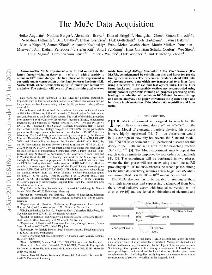
Fig. 1. Schematic view of the phase I Mu3e detector (cut along the beamaxis, around which it is cylindrically symmetric). Muons are stopped on ahollow double-cone target surrounded by two layers of vertex pixel sensors.Scintillating fibres provide a first timing measurement, followed by theouter pixel layers. In forward and backward direction, further pixel layerscomplemented by scintillating tiles greatly improve the momentum and timingmeasurements of particles re-curling in the magnetic field.
arX
iv:2
010.
1564
8v2
[ph
ysic
s.in
s-de
t] 2
0 Ja
n 20
21
2
Detector adaptorboard
Detector adaptorboards
FPGASi5345
MuPix
Fire�y
CPLD
Inner pixel layersU
p to
12
Sens
or A
SICs
10 F
ront
-end
boa
rds
1.25 Gbit/s LVDS links
FPGASi5345
MuPix
Fire�y
CPLD
Outer pixel layers
Up
to 3
6 Se
nsor
ASI
Cs78
Fro
nt-e
nd b
oard
s
1.25 Gbit/s LVDS link
Back
plan
e
CC
Back
plan
e
CC
FPGASi5345
MuTrig
Fire�y
CPLD
Scintillating �bres
8 TD
C A
SICs
12 F
ront
-end
boa
rds
1.25 Gbit/s LVDS link
Back
plan
e
CC
FPGASi5345
MuTrig
Fire�y
CPLD
Scintillating tiles
13 T
DC
ASI
Cs14
Fro
nt-e
nd b
oard
s
1.25 Gbit/s LVDS link
Back
plan
e
CC
Fibre fanout rack
Det
ecto
r Mag
net
6.25 Gbit/s Optical links
366.25 Gbit/s Optical links
MiniPodsPC
FPGA
PCIe
MiniPods
...
...
...
Cent
ral D
etec
tor
Switc
hing
Boa
rd
126.25 Gbit/s Optical links
MiniPods
FPGA
MiniPods
...
...
...Fibr
e D
etec
tor
Switc
hing
Boa
rd
336.25 Gbit/s Optical links
MiniPods
FPGA
MiniPods
...
...
...
Recu
lrl S
tatio
n U
pstr
eam
Switc
hing
Boa
rd
336.25 Gbit/s Optical links
MiniPods
FPGA
MiniPods
...
...
...
Recu
rl St
atio
n D
owns
trea
m
Switc
hing
Boa
rd
PC
PCIe
PC
PCIe
PC
PCIe
QSFP
FPGA
DDR
PCIe
RAM
CPU
16
GPU
Switching PC Switching PC Switching PC Switching PC
ClockReceivingCard
QSFP
FPGA
DDR
PCIe
RAM
CPU
16
GPU ClockReceivingCard
QSFP
FPGA
DDR
PCIe
RAM
CPU
16
GPU ClockReceivingCard
16 16 16
...(12 farm PCs
in total)
Farm PC Farm PC Farm PC
Fire�y Fire�y Fire�y Fire�y12 x 12 x
12 12
144 144
12 12
Fan-outs Fan-outs
12 12
Fire�y4
12 12
4
Fire�y Fire�y
4
Si53458
FPGA8
Clock & Reset Box
SFP+ SFP+ SFP+ SFP+
Data Collection Server Mass Storage
Ethernet125 MHz System Clock
1.25 Gbit/s Reset & Control
Hit data
Monitoring data
Con�guration data
Electrical link
Optical link
Detector adaptorboards
Detector adaptorboard
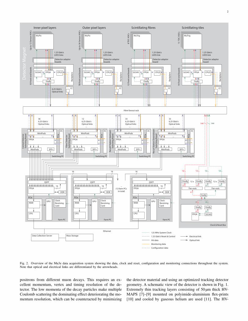
Fig. 2. Overview of the Mu3e data acquisition system showing the data, clock and reset, configuration and monitoring connections throughout the system.Note that optical and electrical links are differentiated by the arrowheads.
positrons from different muon decays. This requires an ex-cellent momentum, vertex and timing resolution of the de-tector. The low momenta of the decay particles make multipleCoulomb scattering the dominating effect deteriorating the mo-mentum resolution, which can be counteracted by minimizing
the detector material and using an optimized tracking detectorgeometry. A schematic view of the detector is shown in Fig. 1.Extremely thin tracking layers consisting of 50 µm thick HV-MAPS [7]–[9] mounted on polyimide-aluminium flex-prints[10] and cooled by gaseous helium are used [11]. The HV-
3
MAPS for Mu3e, the MuPix ASICs [12]–[17], perform on-sensor digitization and zero-suppression and send out hit datavia up to three 1.25 Gbit/s Low-Voltage Differential Signalling(LVDS) links. Combinatorial background can be further sup-pressed by precise timing measurements, which are providedby scintillating fibres (SciFi, [18]) and tiles [19], read outby Silicon Photomultipliers (SiPMs). The SiPM signals aredigitized using the custom MuTRiG ASIC [20], [21], whichalso provides a 1.25 Gbit/s LVDS output. The high granularityof the detector combined with the large particle rates producesan enormous amount of data; the Data Acquisition (DAQ)system has to deal with roughly 100 Gbit/s at 108 muons persecond. Table I lists the bandwidth requirements estimatedfrom a detailed, Geant4-based [22] simulation of the Mu3edetector.
Mu3e uses a triggerless, streaming DAQ that employs anetwork of FPGAs and fast optical links [23] to transportall data out of the detector volume to a small farm of PCsequipped with powerful Graphics Processing Units (GPUs) forparticle track and vertex reconstruction. The low momentumof the decay particles combined with the strong magnetic fieldleads to strongly curved tracks. Particles can thus produce hitsin physically distant parts of the detector; see Fig. 1. Theresulting very non-local track finding problem requires thatthe data from the complete detector are available on everyfarm node. The readout network thus rearranges the data suchthat the farm nodes see the complete detector data of differenttime slices.
The Maximum Integrated Data Acquisition System (MIDAS,[24], [25]) is used as the software framework for the Mu3eDAQ. All DAQ PCs run so-called MIDAS Front-ends interact-ing with the DAQ hardware either via PCIExpress (PCIe) orEthernet.
The architecture of the Mu3e DAQ is shown in Fig. 2. Inthis paper, we will discuss the path of data through the systemand introduce the hardware used.
II. THE DAQ SYSTEM
A. Front-end ASICs
The phase I Mu3e experiment will be built from 2844MuPix pixel sensors complemented by scintillating fibres with3072 SiPM readout channels and 5824 scintillating tiles. Thepixel sensors as well as the 278 MuTRiG ASICs reading outthe scintillating detectors send zero-suppressed hit data over8b/10b encoded [26] LVDS links.
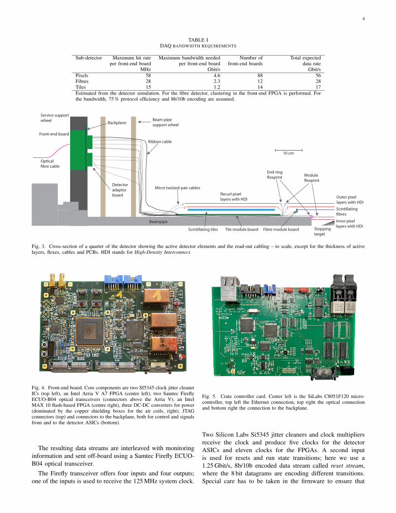
The detector concept with a particle tracking volume outsideof the detector tube and all signal lines routed inside (togetherwith channels for the gaseous helium cooling system, copperbars for power and ground as well as the beam pipe) leadto very tight space constraints for signal cabling; see Fig. 3for an overview. In the case of the pixel detector, the datafirst have to be transported out of the active tracking region,implying that material has to be minimized in order to reducemultiple Coulomb scattering of decay particles. The signalsare thus routed over thin aluminium-polyimide high-densityinterconnects [11] out of the active region. Flexible PCBsconnected by interposers are then used for transferring them
to micro twisted-pair cables leading to the Service SupportWheels (SSWs), located close to the ends of the bore of the3 m long 1 T solenoid magnet. For the inner pixel layers, three1.25 Gbit/s links per pixel sensor, each capable of transmittingabout 30 Mhits/s are connected, whereas in the outer pixellayers, only one link is connected.
For the fibre detector, one 128 channel SiPM array isconnected to one SciFi module board with four MuTRiGASICs. These module boards are then connected via microtwisted-pair cables to the SSW. In case of the tile detector,one MuTRiG chip reads 32 individual SiPMs and thirteenMuTRiGs are collected on one tile module board, which isthen connected to the SSW using a ribbon cable.
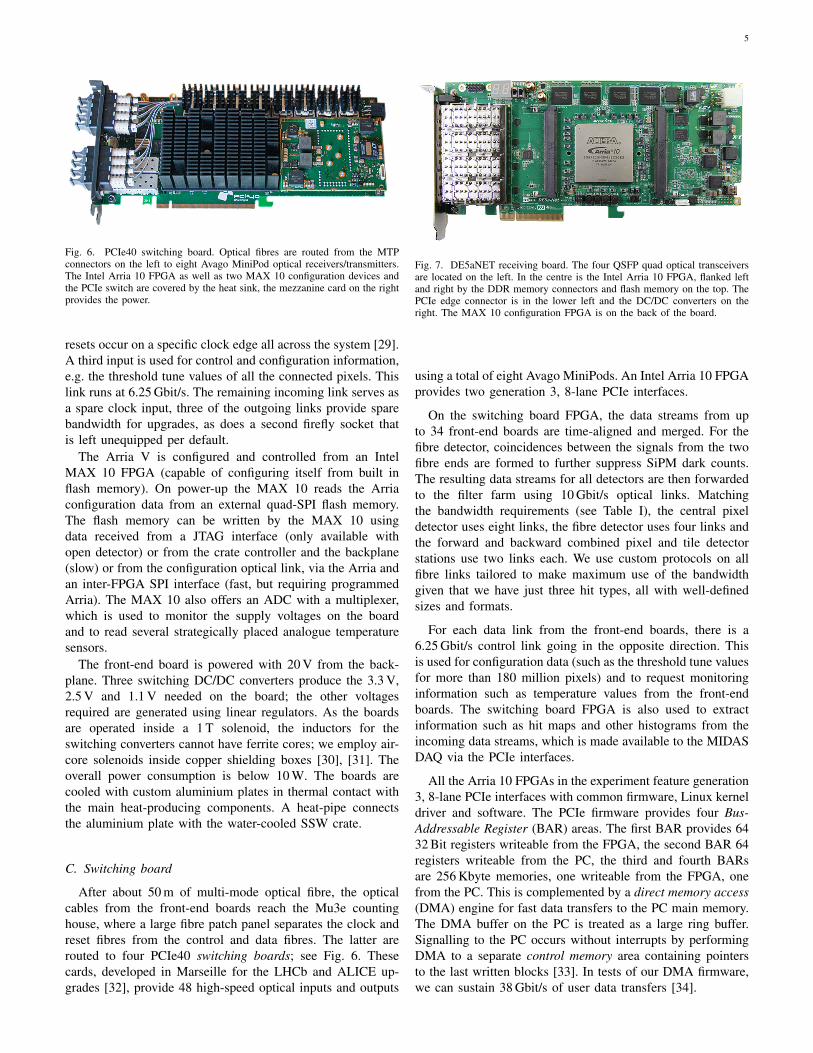
B. Front-end boardA total of 114 Front-End Boards (see Fig. 4) collect the
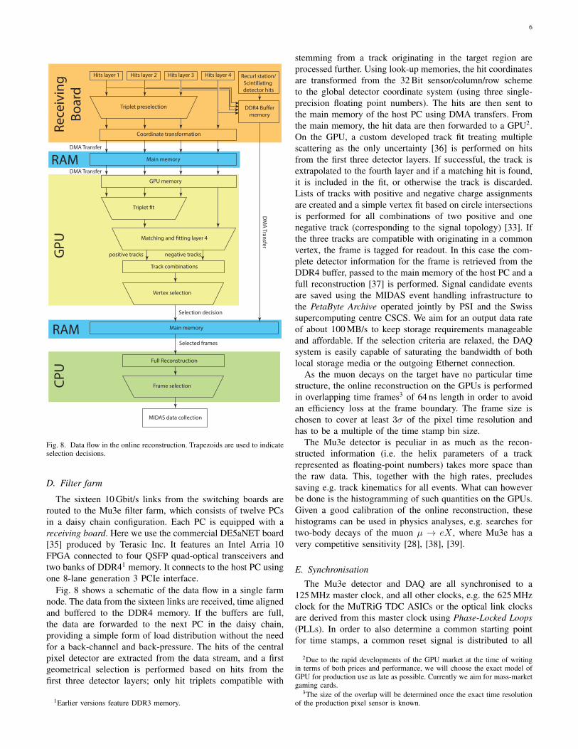
sensor data, perform data processing on an FPGA and thensend the data out of the magnet volume using 6.25 Gbit/soptical links. We decided to use a common front-end boardfor all sub-detectors and do the detector specific signal routingon a detector adaptor board. The euro-card-sized boards sit inquarter-circular crates on the SSW. A backplane links up to16 front-end boards to a crate controller card and connectsup to two detector adaptor boards to a front-end board. Thecrate controller card (see Fig. 5) uses a SiLabs C8051F120micro-controller running a bare-metal C control program. Onone side it connects to each front-end board via the backplane,and on the other side it connects to the experiment’s controlnetwork using the MIDAS Slow Control Bus (MSCB, [27])via either a standard Ethernet network (for tests outside themagnet) or an optical link. Boards can individually be powercycled in case of problems or firmware updates. A dedicatedstand-by power allows temperature measurements in all front-end boards even if their power is off, which might be usefulif problems with the cooling system occur.
Data processing on the front-end board is performed byan Intel Arria V A7 FPGA: The incoming data are 8b/10bdecoded, and hits are separated from monitoring information.The links are continuously monitored by detecting 8b/10bencoding and parity errors as well as deviations from the dataprotocol.
For the pixel detector, a time-walk correction based on themeasured time over threshold is applied to the hit time stamps.The hits are then time sorted using insertion into memory ataddresses determined by the hit time stamp [28]. A list of thehits from each ASIC and each time stamp is generated. Theselists are then processed into a single memory read sequence.Executing this read sequence produces a single, fully time-sorted output stream containing the data from up to 36 inputlinks.
Due to the way the fibre ribbons are matched to the SiPMarrays, particles passing the detector almost always triggermore than one SiPM channel. The hits of the fibre detectorare therefore clustered in time and space on the FPGA. Sup-pression of single hit clusters allows to reduce the bandwidthconsumed by dark counts considerably, which would otherwisedominate over particle signals, especially after irradiation ofthe SiPMs.
4
TABLE IDAQ BANDWIDTH REQUIREMENTS
Sub-detector Maximum hit rate Maximum bandwidth needed Number of Total expectedper front-end board per front-end board front-end boards data rate
MHz Gbit/s Gbit/sPixels 58 4.6 88 56Fibres 28 2.3 12 28Tiles 15 1.2 14 17Estimated from the detector simulation. For the fibre detector, clustering in the front-end FPGA is performed. Forthe bandwidth, 75 % protocol efficiency and 8b/10b encoding are assumed.
Beampipe
Stoppingtarget
Inner pixellayers with HDI
End-ring�exprint Module
�exprint
Scintillating�bres
Outer pixellayers with HDI
Scintillating tiles Tile module board
Recurl pixellayers with HDI
Fibre module board
Micro twisted-pair cables
Ribbon cable
Service support wheel
Front-end board
Detectoradaptorboard
Backplane
Optical�bre cable
Beam pipesupport wheel
10 cm
Fig. 3. Cross-section of a quarter of the detector showing the active detector elements and the read-out cabling – to scale, except for the thickness of activelayers, flexes, cables and PCBs. HDI stands for High-Density Interconnect.
Fig. 4. Front-end board. Core components are two SI5345 clock jitter cleanerICs (top left), an Intel Arria V A7 FPGA (centre left), two Samtec FireflyECUO-B04 optical transceivers (connectors above the Arria V), an IntelMAX 10 flash-based FPGA (centre right), three DC-DC converters for power(dominated by the copper shielding boxes for the air coils, right), JTAGconnectors (top) and connectors to the backplane, both for control and signalsfrom and to the detector ASICs (bottom).
The resulting data streams are interleaved with monitoringinformation and sent off-board using a Samtec Firefly ECUO-B04 optical transceiver.
The Firefly transceiver offers four inputs and four outputs;one of the inputs is used to receive the 125 MHz system clock.
Fig. 5. Crate controller card. Center left is the SiLabs C8051F120 micro-controller, top left the Ethernet connection, top right the optical connectionand bottom right the connection to the backplane.
Two Silicon Labs Si5345 jitter cleaners and clock multipliersreceive the clock and produce five clocks for the detectorASICs and eleven clocks for the FPGAs. A second inputis used for resets and run state transitions; here we use a1.25 Gbit/s, 8b/10b encoded data stream called reset stream,where the 8 bit datagrams are encoding different transitions.Special care has to be taken in the firmware to ensure that
5
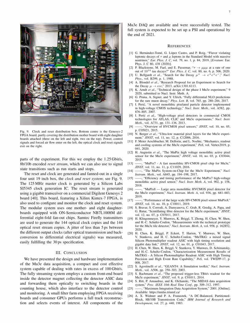
Fig. 6. PCIe40 switching board. Optical fibres are routed from the MTPconnectors on the left to eight Avago MiniPod optical receivers/transmitters.The Intel Arria 10 FPGA as well as two MAX 10 configuration devices andthe PCIe switch are covered by the heat sink, the mezzanine card on the rightprovides the power.
resets occur on a specific clock edge all across the system [29].A third input is used for control and configuration information,e.g. the threshold tune values of all the connected pixels. Thislink runs at 6.25 Gbit/s. The remaining incoming link serves asa spare clock input, three of the outgoing links provide sparebandwidth for upgrades, as does a second firefly socket thatis left unequipped per default.
The Arria V is configured and controlled from an IntelMAX 10 FPGA (capable of configuring itself from built inflash memory). On power-up the MAX 10 reads the Arriaconfiguration data from an external quad-SPI flash memory.The flash memory can be written by the MAX 10 usingdata received from a JTAG interface (only available withopen detector) or from the crate controller and the backplane(slow) or from the configuration optical link, via the Arria andan inter-FPGA SPI interface (fast, but requiring programmedArria). The MAX 10 also offers an ADC with a multiplexer,which is used to monitor the supply voltages on the boardand to read several strategically placed analogue temperaturesensors.
The front-end board is powered with 20 V from the back-plane. Three switching DC/DC converters produce the 3.3 V,2.5 V and 1.1 V needed on the board; the other voltagesrequired are generated using linear regulators. As the boardsare operated inside a 1 T solenoid, the inductors for theswitching converters cannot have ferrite cores; we employ air-core solenoids inside copper shielding boxes [30], [31]. Theoverall power consumption is below 10 W. The boards arecooled with custom aluminium plates in thermal contact withthe main heat-producing components. A heat-pipe connectsthe aluminium plate with the water-cooled SSW crate.
C. Switching board
After about 50 m of multi-mode optical fibre, the opticalcables from the front-end boards reach the Mu3e countinghouse, where a large fibre patch panel separates the clock andreset fibres from the control and data fibres. The latter arerouted to four PCIe40 switching boards; see Fig. 6. Thesecards, developed in Marseille for the LHCb and ALICE up-grades [32], provide 48 high-speed optical inputs and outputs
Fig. 7. DE5aNET receiving board. The four QSFP quad optical transceiversare located on the left. In the centre is the Intel Arria 10 FPGA, flanked leftand right by the DDR memory connectors and flash memory on the top. ThePCIe edge connector is in the lower left and the DC/DC converters on theright. The MAX 10 configuration FPGA is on the back of the board.
using a total of eight Avago MiniPods. An Intel Arria 10 FPGAprovides two generation 3, 8-lane PCIe interfaces.
On the switching board FPGA, the data streams from upto 34 front-end boards are time-aligned and merged. For thefibre detector, coincidences between the signals from the twofibre ends are formed to further suppress SiPM dark counts.The resulting data streams for all detectors are then forwardedto the filter farm using 10 Gbit/s optical links. Matchingthe bandwidth requirements (see Table I), the central pixeldetector uses eight links, the fibre detector uses four links andthe forward and backward combined pixel and tile detectorstations use two links each. We use custom protocols on allfibre links tailored to make maximum use of the bandwidthgiven that we have just three hit types, all with well-definedsizes and formats.
For each data link from the front-end boards, there is a6.25 Gbit/s control link going in the opposite direction. Thisis used for configuration data (such as the threshold tune valuesfor more than 180 million pixels) and to request monitoringinformation such as temperature values from the front-endboards. The switching board FPGA is also used to extractinformation such as hit maps and other histograms from theincoming data streams, which is made available to the MIDASDAQ via the PCIe interfaces.
All the Arria 10 FPGAs in the experiment feature generation3, 8-lane PCIe interfaces with common firmware, Linux kerneldriver and software. The PCIe firmware provides four Bus-Addressable Register (BAR) areas. The first BAR provides 6432 Bit registers writeable from the FPGA, the second BAR 64registers writeable from the PC, the third and fourth BARsare 256 Kbyte memories, one writeable from the FPGA, onefrom the PC. This is complemented by a direct memory access(DMA) engine for fast data transfers to the PC main memory.The DMA buffer on the PC is treated as a large ring buffer.Signalling to the PC occurs without interrupts by performingDMA to a separate control memory area containing pointersto the last written blocks [33]. In tests of our DMA firmware,we can sustain 38 Gbit/s of user data transfers [34].
6
Rece
ivin
gBo
ard
GPU
RAM
RAM
CPU
Hits layer 1 Hits layer 2 Hits layer 3 Hits layer 4 Recurl station/Scintillating detector hits
Triplet preselection
Main memory
GPU memory
Triplet �t
Coordinate transformation
Matching and �tting layer 4
Track combinations
Vertex selection
Main memory
MIDAS data collection
positive tracks negative tracks
Selection decision
Selected frames
DMA Transfer
DMA Transfer
DDR4 Bu�ermemory
DM
A Transfer
Full Reconstruction
Frame selection
Fig. 8. Data flow in the online reconstruction. Trapezoids are used to indicateselection decisions.
D. Filter farm
The sixteen 10 Gbit/s links from the switching boards arerouted to the Mu3e filter farm, which consists of twelve PCsin a daisy chain configuration. Each PC is equipped with areceiving board. Here we use the commercial DE5aNET board[35] produced by Terasic Inc. It features an Intel Arria 10FPGA connected to four QSFP quad-optical transceivers andtwo banks of DDR41 memory. It connects to the host PC usingone 8-lane generation 3 PCIe interface.
Fig. 8 shows a schematic of the data flow in a single farmnode. The data from the sixteen links are received, time alignedand buffered to the DDR4 memory. If the buffers are full,the data are forwarded to the next PC in the daisy chain,providing a simple form of load distribution without the needfor a back-channel and back-pressure. The hits of the centralpixel detector are extracted from the data stream, and a firstgeometrical selection is performed based on hits from thefirst three detector layers; only hit triplets compatible with
1Earlier versions feature DDR3 memory.
stemming from a track originating in the target region areprocessed further. Using look-up memories, the hit coordinatesare transformed from the 32 Bit sensor/column/row schemeto the global detector coordinate system (using three single-precision floating point numbers). The hits are then sent tothe main memory of the host PC using DMA transfers. Fromthe main memory, the hit data are then forwarded to a GPU2.On the GPU, a custom developed track fit treating multiplescattering as the only uncertainty [36] is performed on hitsfrom the first three detector layers. If successful, the track isextrapolated to the fourth layer and if a matching hit is found,it is included in the fit, or otherwise the track is discarded.Lists of tracks with positive and negative charge assignmentsare created and a simple vertex fit based on circle intersectionsis performed for all combinations of two positive and onenegative track (corresponding to the signal topology) [33]. Ifthe three tracks are compatible with originating in a commonvertex, the frame is tagged for readout. In this case the com-plete detector information for the frame is retrieved from theDDR4 buffer, passed to the main memory of the host PC and afull reconstruction [37] is performed. Signal candidate eventsare saved using the MIDAS event handling infrastructure tothe PetaByte Archive operated jointly by PSI and the Swisssupercomputing centre CSCS. We aim for an output data rateof about 100 MB/s to keep storage requirements manageableand affordable. If the selection criteria are relaxed, the DAQsystem is easily capable of saturating the bandwidth of bothlocal storage media or the outgoing Ethernet connection.
As the muon decays on the target have no particular timestructure, the online reconstruction on the GPUs is performedin overlapping time frames3 of 64 ns length in order to avoidan efficiency loss at the frame boundary. The frame size ischosen to cover at least 3σ of the pixel time resolution andhas to be a multiple of the time stamp bin size.
The Mu3e detector is peculiar in as much as the recon-structed information (i.e. the helix parameters of a trackrepresented as floating-point numbers) takes more space thanthe raw data. This, together with the high rates, precludessaving e.g. track kinematics for all events. What can howeverbe done is the histogramming of such quantities on the GPUs.Given a good calibration of the online reconstruction, thesehistograms can be used in physics analyses, e.g. searches fortwo-body decays of the muon µ → eX , where Mu3e has avery competitive sensitivity [28], [38], [39].
E. Synchronisation
The Mu3e detector and DAQ are all synchronised to a125 MHz master clock, and all other clocks, e.g. the 625 MHzclock for the MuTRiG TDC ASICs or the optical link clocksare derived from this master clock using Phase-Locked Loops(PLLs). In order to also determine a common starting pointfor time stamps, a common reset signal is distributed to all
2Due to the rapid developments of the GPU market at the time of writingin terms of both prices and performance, we will choose the exact model ofGPU for production use as late as possible. Currently we aim for mass-marketgaming cards.
3The size of the overlap will be determined once the exact time resolutionof the production pixel sensor is known.
7
Fig. 9. Clock and reset distribution box. Bottom centre is the Genesys-2FPGA board, partly covering the distribution mother board with eight daughterboards attached (three on the left and right, two on the top). Power, controlsignals and forced air flow enter on the left, the optical clock and reset signalsexit on the right.
parts of the experiment. For this we employ the 1.25 Gbit/s,8b/10b encoded reset stream, which we can also use to signalstate transitions such as run starts and stops.
The reset and clock are generated and fanned-out in a singlefour unit 19 inch box, the clock and reset system; see Fig. 9.The 125 MHz master clock is generated by a Silicon LabsSI5345 clock generation IC. The reset stream is generatedusing a gigabit transceiver on a commercial Digilent Genesys 2board [40]. This board, featuring a Xilinx Kintex-7 FPGA, isalso used to configure and monitor the clock and reset system.The modular system uses one mother- and eight daughter-boards equipped with ON-Semiconductor NB7L1008M dif-ferential eight-fold fan-out chips. Samtec Firefly transmittersare used to generate the 144 optical clock copies and the 144optical reset stream copies. A jitter of less than 5 ps betweenthe different output clocks (after optical transmission and back-conversion to differential electrical signals) was measured,easily fulfilling the 30 ps specification.
III. CONCLUSION
We have presented the design and hardware implementationof the Mu3e data acquisition, a compact and cost effectivesystem capable of dealing with rates in excess of 100 Gbit/s.The fully streaming system employs a custom front-end boardinside the detector magnet collecting the detector ASIC dataand forwarding them optically to switching boards in thecounting house, which also interface to the detector controland monitoring. A small filter farm employing FPGA receivingboards and consumer GPUs performs a full track reconstruc-tion and selects events of interest. All components of the
Mu3e DAQ are available and were successfully tested. Thefull system is expected to be set up a PSI and operational bythe end of 2021.
REFERENCES
[1] G. Hernandez-Tome, G. Lopez Castro, and P. Roig, “Flavor violatingleptonic decays of τ and µ leptons in the Standard Model with massiveneutrinos,” Eur. Phys. J. C, vol. 79, no. 1, p. 84, 2019, [Erratum: Eur.Phys. J. C 80, 438 (2020)].
[2] P. Blackstone, M. Fael, and E. Passemar, “τ → µµµ at a rate of oneout of 1014 tau decays?” Eur. Phys. J. C, vol. 80, no. 6, p. 506, 2020.
[3] U. Bellgardt et al., “Search for the Decay µ+ → e+e+e−,” Nucl.Phys., vol. B299, p. 1, 1988.
[4] A. Blondel et al., “Research Proposal for an Experiment to Search forthe Decay µ→ eee,” 2013, arXiv:1301.6113.
[5] K. Arndt et al., “Technical design of the phase I Mu3e experiment,” 92020, submitted to Nucl. Instr. Meth. A.
[6] G. Pruna, A. Signer, and Y. Ulrich, “Fully differential NLO predictionsfor the rare muon decay,” Phys. Lett. B, vol. 765, pp. 280–284, 2017.
[7] I. Peric, “A novel monolithic pixelated particle detector implementedin high-voltage CMOS technology,” Nucl. Instr. Meth., vol. A582, pp.876–885, 2007.
[8] I. Peric et al., “High-voltage pixel detectors in commercial CMOStechnologies for ATLAS, CLIC and Mu3e experiments,” Nucl. Instr.Meth., vol. A731, pp. 131–136, 2013.
[9] ——, “Overview of HVCMOS pixel sensors,” JINST, vol. 10, no. 05,p. C05021, 2015.
[10] N. Berger et al., “Ultra-low material pixel layers for the Mu3e experi-ment,” JINST, vol. 11, no. 12, p. C12006, 2016.
[11] F. Meier Aeschbacher, M. Deflorin, and L. Noehte, “Mechanics, readoutand cooling systems of the Mu3e experiment,” PoS, vol. Vertex2019, p.041, 2020.
[12] H. Augustin et al., “The MuPix high voltage monolithic active pixelsensor for the Mu3e experiment,” JINST, vol. 10, no. 03, p. C03044,2015.
[13] ——, “MuPix7 - A fast monolithic HV-CMOS pixel chip for Mu3e,”JINST, vol. 11, no. 11, p. C11029, 2016.
[14] ——, “The MuPix System-on-Chip for the Mu3e Experiment,” Nucl.Instrum. Meth., vol. A845, pp. 194–198, 2017.
[15] ——, “Efficiency and timing performance of the MuPix7 high-voltagemonolithic active pixel sensor,” Nucl. Instr. Meth. A, vol. 902, p. 158,2018.
[16] ——, “MuPix8 — Large area monolithic HVCMOS pixel detector forthe Mu3e experiment,” Nucl. Instrum. Meth. A, vol. 936, pp. 681–683,2019.
[17] ——, “Performance of the large scale HV-CMOS pixel sensor MuPix8,”JINST, vol. 14, no. 10, p. C10011, 2019.
[18] S. Bravar, S. Corrodi, A. Damyanova, C. Grab, R. Gredig, A. Papa, andG. Rutar, “Scintillating fibre detector for the Mu3e experiment,” JINST,vol. 12, no. 07, p. C07011, 2017.
[19] H. Klingenmeyer, Y. Munwes, K. Briggl, T. Zhong, H. Chen, W. Shen,and H.-C. Schultz-Coulon, “Measurements with the technical prototypefor the Mu3e tile detector,” Nucl. Instrum. Meth. A, vol. 958, p. 162852,2020.
[20] H. Chen, K. Briggl, P. Eckert, T. Harion, Y. Munwes, W. Shen,V. Stankova, and H. C. Schultz-Coulon, “MuTRiG: a mixed signalSilicon Photomultiplier readout ASIC with high timing resolution andgigabit data link,” JINST, vol. 12, no. 01, p. C01043, 2017.
[21] H. Chen, W. Shen, K. Briggl, V. Stankova, Y. Munwes, D. Schimansky,and H.-C. Schultz-Coulon, “Characterization Measurement Results ofMuTRiG - A Silicon Photomultiplier Readout ASIC with High TimingPrecision and High Event Rate Capability,” PoS, vol. TWEPP-17, p.008, 2017.
[22] S. Agostinelli et al., “GEANT4: A Simulation toolkit,” Nucl. Instrum.Meth., vol. A506, pp. 250–303, 2003.
[23] S. Bachmann et al., “The proposed trigger-less TBit/s readout for theMu3e experiment,” JINST, vol. 9, p. C01011, 2014.
[24] S. Ritt, P. Amaudruz, and K. Olchanski, “The MIDAS data acquisitionsystem,” Proc. IEEE 10th Real Time Conf., pp. 309–312, 1997.
[25] ——, “Maximum Integration Data Acquisition System,” 2001. [Online].Available: https://midas.triumf.ca/
[26] A. X. Widmer and P. A. Franaszek, “A DC-Balanced, Partitioned-Block, 8B/10B Transmission Code,” IBM Journal of Research andDevelopment, vol. 27, p. 440, 1983.
8
[27] S. Ritt and R. Schmidt, “MSCB (MIDAS Slow Control Bus),” 2001.[Online]. Available: https://elog.psi.ch/mscb/
[28] A.-K. Perrevoort, “Sensitivity Studies on New Physics in the Mu3eExperiment and Development of Firmware for the Front-End of theMu3e Pixel Detector,” PhD Thesis, Heidelberg University, 2018.
[29] M. Muller, “A Control System for the Mu3e Data Acquisition,” MasterThesis, Mainz University, 2019.
[30] M. Hesping, “Air Coils for Powering the Mu3e Experiment,” BachelorThesis, Mainz University, 2019.
[31] S. Gagneur, “Developement of a DC-DC Converter for the Mu3eDetector,” Master Thesis, Mainz University, 2020.
[32] J. P. Cachemiche, P. Y. Duval, F. Hachon, R. Le Gac, and F. Rethore,“The PCIe-based readout system for the LHCb experiment,” JINST,vol. 11, no. 02, p. P02013, 2016.
[33] D. vom Bruch, “Pixel Sensor Evaluation and Online Event Selection forthe Mu3e Experiment,” Ph.D. dissertation, Heidelberg University, 2017.
[34] M. Koppel, “Data Flow in the Mu3e Filter Farm,” Master Thesis, MainzUniversity, 2019.
[35] “DE5a-NET FPGA Development Kit User Manual,” Terasic Inc, Tech.Rep., 2019.
[36] N. Berger, M. Kiehn, A. Kozlinskiy, and A. Schoning, “A New Three-Dimensional Track Fit with Multiple Scattering,” Nucl. Instrum. Meth.,vol. A844, p. 135, 2017.
[37] A. Kozlinskiy, “Track reconstruction for the Mu3e experiment based ona novel Multiple Scattering fit,” EPJ Web Conf., vol. 150, p. 00005,2017.
[38] A.-K. Perrevoort, “The Rare and Forbidden: Testing Physics Beyond theStandard Model with Mu3e,” SciPost Phys. Proc., vol. 1, p. 052, 2019.
[39] L. Calibbi, D. Redigolo, R. Ziegler, and J. Zupan, “Looking forward toLepton-flavor-violating ALPs,” 6 2020.
[40] “The Digilent Genesys 2 Kintex-7 FPGA developmentboard.” [Online]. Available: https://reference.digilentinc.com/reference/programmable-logic/genesys-2/