Spontaneous Surface Collapse and Reconstruction …structure in the bulk, the collapsed surface is...
40
1 Spontaneous Surface Collapse and Reconstruction in Antiferromagnetic Topological Insulator MnBi 2 Te 4 Fuchen Hou 1 *, Qiushi Yao 1 *, Chun-Sheng Zhou 1 , Xiao-Ming Ma 1 , Mengjiao Han 1 , Yu- Jie Hao 1 , Xuefeng Wu 1 , Yu Zhang 1,3 , Hongyi Sun 1 , Chang Liu 1,2 , Yue Zhao 1,2† , Qihang Liu 1,2,4† , Junhao Lin 1† 1 Department of Physics, Southern University of Science and Technology, Shenzhen 518055, Guangdong, P. R. China 2 Shenzhen Institute for Quantum Science and Engineering, Southern University of Science and Technology, Shenzhen 518055, P. R. China 3 Department of Physics, University of Hong Kong, Hong Kong, P. R. China 4 Guangdong Provincial Key Laboratory for Computational Science and Material Design, Southern University of Science and Technology, Shenzhen 518055, China *These authors contributed equally to this work. † Corresponding author. E-mail: [email protected]; [email protected]; [email protected] Abstract MnBi2Te4 is an antiferromagnetic topological insulator which stimulates intense interests due to the exotic quantum phenomena and promising device applications. Surface structure is a determinant factor to understand the novel magnetic and topological behavior of MnBi2Te4, yet its precise atomic structure remains elusive. Here, we discovered a spontaneous surface collapse and reconstruction in few-layer MnBi2Te4 exfoliated under delicate protection. Instead of the ideal septuple-layer structure in the bulk, the collapsed surface is shown to reconstruct as Mn-doped Bi2Te3 quintuple-layer and MnxBiyTe double-layer with a clear van der Waals gap in between. Combining with first-principles calculations, such spontaneous surface collapse is attributed to the abundant intrinsic Mn-Bi antisite defects and tellurium vacancy in the exfoliated surface, which is further supported by in-situ annealing and electron
Transcript of Spontaneous Surface Collapse and Reconstruction …structure in the bulk, the collapsed surface is...
1
Spontaneous Surface Collapse and Reconstruction in
Antiferromagnetic Topological Insulator MnBi2Te4
Fuchen Hou1*, Qiushi Yao1*, Chun-Sheng Zhou1, Xiao-Ming Ma1, Mengjiao Han1, Yu-
Jie Hao1, Xuefeng Wu1, Yu Zhang1,3, Hongyi Sun1, Chang Liu1,2, Yue Zhao1,2†, Qihang
Liu1,2,4†, Junhao Lin1†
1Department of Physics, Southern University of Science and Technology, Shenzhen
518055, Guangdong, P. R. China 2Shenzhen Institute for Quantum Science and Engineering, Southern University of
Science and Technology, Shenzhen 518055, P. R. China 3Department of Physics, University of Hong Kong, Hong Kong, P. R. China 4Guangdong Provincial Key Laboratory for Computational Science and Material
Design, Southern University of Science and Technology, Shenzhen 518055, China
*These authors contributed equally to this work. †Corresponding author. E-mail: [email protected]; [email protected];
Abstract
MnBi2Te4 is an antiferromagnetic topological insulator which stimulates intense
interests due to the exotic quantum phenomena and promising device applications.
Surface structure is a determinant factor to understand the novel magnetic and
topological behavior of MnBi2Te4, yet its precise atomic structure remains elusive. Here,
we discovered a spontaneous surface collapse and reconstruction in few-layer
MnBi2Te4 exfoliated under delicate protection. Instead of the ideal septuple-layer
structure in the bulk, the collapsed surface is shown to reconstruct as Mn-doped Bi2Te3
quintuple-layer and MnxBiyTe double-layer with a clear van der Waals gap in between.
Combining with first-principles calculations, such spontaneous surface collapse is
attributed to the abundant intrinsic Mn-Bi antisite defects and tellurium vacancy in the
exfoliated surface, which is further supported by in-situ annealing and electron

2
irradiation experiments. Our results shed light on the understanding of the intricate
surface-bulk correspondence of MnBi2Te4, and provide insightful perspective of the
surface-related quantum measurements in MnBi2Te4 few-layer devices.
Keywords: Surface reconstruction, MnBi2Te4, magnetic topological insulator, anti-site
defects, tellurium vacancy, in-situ surface dynamics
Introduction
Magnetic topological quantum materials have stimulated intense research interest
due to the interplay between magnetism and topology which results in emerging
quantum phenomenon1–4. Examples include quantum anomalous Hall effect (QAHE)3–
5, Weyl semimetallic states6,7, topological axion states8 and Majorana fermions2,9, etc,
enabling potential applications in dissipationless electronic and quantum computing10.
In the early research, a magnetic topological insulator (TI) is achieved by magnetically
doping a TI thin film, in order to study the QAHE3–5. However, the random distribution
of magnetic dopants introduces impurity scattering together with the ferromagnetic
ordering, limiting the temperature for the realization of QAHE. Very recently, the
tetradymite-type MnBi2Te4 compound was discovered as an intrinsic antiferromagnetic
(AFM) TI in A-type AFM ground state with out-of-plane magnetic moments11–19.
Although the existence of long-range magnetic order explicitly breaks the time-reversal
symmetry, which is nevertheless preserved in conventional Z2 TI1,2, a new type of Z2
invariant can be defined in MnBi2Te4, as long as a combined symmetry between time-

3
reversal and fractional translation is preserved11,20,21. As a result, MnBi2Te4 provide an
ideal platform of magnetic TI to realize QAHE and axion insulator state15,17,22, etc.
On the other hand, there are still discrepancies between theoretical expectations
and experimental facts in MnBi2Te4. For instance, theoretical predictions and some
experimental observations declared a sizable magnetic gap at the surface of bulk
MnBi2Te411–15, while recent report shows an unambiguously gapless Dirac cone at the
(00l) surface of MnBi2Te4 crystal by using the high-resolution angle resolved
photoemission spectroscopy (ARPES)16,23,24. Such inconsistency implies that the
surface structure is a key factor requiring precise measurements, which may affect
many of the corresponding novel magnetic and topological behavior in MnBi2Te4, such
as the QAHE in odd-layers and the zero Hall plateau as an indicator of axion state in
even-layers11,17,18. Apparently, most of the previous results consider the surface
structure using the ideal septuple-layer (SL) MnBi2Te4 lattice 11–19, which, on the other
hand, lacks direct proof to connect the bridge between theory and experiments.
Since the surface-bulk correspondence is the kernel of topological properties, in
this paper, we systematically studied the atomic structure of the surface in MnBi2Te4
few layers with intended surface protection. Using cross-sectional scanning
transmission electron microscopy (STEM) imaging and atomic electron energy loss
spectroscopy (EELS), we unambiguously determine the surface of few-layer MnBi2Te4
to be Mn-doped Bi2Te3 quintuple-layer (QL) decorated with crystalline/amorphous
MnxBiyTe double-layer (DL) rather than the ideal SL layered structure, i.e., a
spontaneous surface collapse and reconstruction occurred during the mechanical

4
exfoliation. Such surface collapse is highly reproducible in all samples we measured.
We further discovered that Bi-Mn anti-site defects were omnipresent in bulk MnBi2Te4.
Combining the density functional theory (DFT) calculations, we unveiled the origin of
the surface collapse in few-layer MnBi2Te4 as a result of the synergistic interaction
between the Bi-Mn anti-site defects and surface tellurium vacancies that unavoidably
formed even in inert gas environment due to trace of oxygen, which makes the as-
observed reconstructed surface preferential in energy landscape. Similar surface
collapse and reconstruction is reproduced by heating the intact SL surface exfoliated in
ultrahigh vacuum as probed by atomic scanning tunneling microscopy (STM), and by
electron irradiation in STEM which simultaneously monitor the dynamical surface
collapse and reconstruction process atom-by-atom. These experiments further verified
that the spontaneous surface collapse and reconstruction occurred in a well-controlled
inert gas environment, is indeed induced by surface Te vacancy. To date, most of the
few-layer MnBi2Te4 devices, in which the exotic quantum phenomena are observed, are
prepared in inert gas environment, where we believe the as-observed spontaneous
surface collapse can still be triggered by the trace of oxygen. Our findings of the
spontaneous surface collapse and reconstruction not only set notes on the fabrication of
MnBi2Te4 few-layer devices, but also bring new insights in understanding the emerging
quantum phenomena in this intrinsic magnetic insulator.
Results and Discussion:
Atomic structure of the collapsed surface in exfoliated MnBi2Te4 few layer

5
MnBi2Te4 single crystal is a member of van der Waals (VDW) layered materials.
A single VDW layer of MnBi2Te4 consists of alternating Bi-Mn-Bi layer intercalated
by Te, forming a SL structure. Its antiferromagnetism originates from the middle Mn
cations with a super-exchanged interlayer interaction between adjacent Mn layers.
Figure 1a shows the XRD measurement of the parent MnBi2Te4 crystal with sharp and
intense peaks that follow the (00l), l = 3n, diffraction rule, which agree quantitatively
with those in the standard PDF files. In addition, X-ray photoelectron spectroscopy
(XPS) characterization on the MnBi2Te4 single crystal reveals the core level peaks of
Mn 2p, Bi 4f and Te 3d (Fig. S1) without any impurity signal from other crystalline
phases and elements, indicating the high quality of the parent single crystal. The fresh
cleaved surface of MnBi2Te4 crystal was initially investigated by high resolution atomic
force microscopy (AFM) operated in the same inert gas environment. A rough surface
was seen with steps ranging from 2-6 Å (1-3 atomic layers) (Fig. S2), suggesting a
possible disordered surface structure. We then performed cross-section study in order
to obtain atomic information of the surface. The surface was intentionally protected by
graphite, ensuring minimum surface degradation during cross-section sample
fabrication (See methods).
Figure 1b shows a low-magnified high-angle annular dark field (HAADF) STEM
image of the as-prepared MnBi2Te4 few-layer cross-section, taken from the [110]
direction. The graphite appears dark contrast due to its relative light atomic weight in
the STEM image. Zoom-in images with atomic resolution of the surface and bulk are
exhibited in Figs. 1c and 1e, respectively. Comparison of the two readily shows an

6
apparent deviation of the surface structure: it is a five-atom layers instead of seven in
surface, similar to the atomic structure of TI Bi2Te3 (Te-Bi-Te-Bi-Te) viewed along the
c-axis, known as QL structure (atomic model is shown in Fig. 1d). In contrast, the
atomic structure of the bulk MnBi2Te4 (Fig. 1e) is consistent with the previous
reports11,12,14, showing a SL structure (Te1-Bi-Te2-Mn-Te2-Bi-Te1) as depicted by the
atomic model in Fig. 1f. Quantitative energy dispersive spectrum (EDS) mapping (see
methods) further revealed the chemical composition of the surface to be mainly
consisted of Bi and Te with trivial Mn. The ratio of Mn, Bi and Te at the surface QL
layer, highlighted by the red dashed rectangle in Fig. 1g, is estimated as ~ 0.3:1.8:3 (Fig.
1h), while reaching the normal 1:2:4 ratio below the surface (Fig. S3).
Above the QL structure, an amorphous layer with brighter contrast than the nearby
graphite protection layer is observed. This amorphous layer separated from the QL
surface with a clear VDW gap, as highlighted by red dashed lines in Fig. 1c. Moreover,
crystalline structure with a DL height was occasionally observed to be embedded in
such amorphous layer, which are highlighted by the white arrows. A larger view of the
surface (Fig. 1g) further manifested that these tiny crystalline structures are
omnipresent above the surface, yet gapped by amorphous layers in between. EDS
results of such amorphous layer and embedded crystalline quantum island (highlighted
by the red dashed rectangle in Fig. 1g) clearly reveal that, in contrast to the QL layer,
the major element is Mn and Te while with trivial Bi. The element ratio among Mn, Bi
and Te is ~ 0.7:0.2:1 (Fig. 1i).
The cross-sectional results pointed to a key finding that the surface of the as-

7
prepared MnBi2Te4 few-layer sample underwent a spontaneous collapse even with
intentional surface protection during the mechanical exfoliation in inert gas
environment. Instead of the ideal SL model with chemical composition Mn:Bi:Te of
1:2:4, which is the case below the surface as verified by quantitative EDS, the realistic
surface split into a Bi-rich QL plus a Mn-rich DL crystalline/amorphous layer, with a
complementary elemental distribution as 0.3:1.8:3 and 0.7:0.2:1, respectively. Such
surface collapse and reconstruction are highly reproducible in all samples we measured,
even in a mild transfer without heating during the drop-down process of the protection
graphite layer. Mn-doped QL Bi2Te3 is stable as reported previously13, however, on the
other hand the DL Bi-rich MnTe is theoretically unstable (See Supplementary Section
Ⅱ for more detail), thus turning into amorphous phase once formed. The existence of
the island-like DL crystalline structure is presumably due to the VDW interaction from
the underlying layers and the local chemical composition fluctuation during the surface
reconstruction.
Detection of the Mn-Bi exchange antisite defects by atomic EELS and intensity
quantification analysis
The unexpected surface collapse and reconstruction may be related to the
superficial chemical stoichiometry variation or surface defects25. To further find out the
hint of the surface collapse, we took the atom-by-atom electron energy-loss
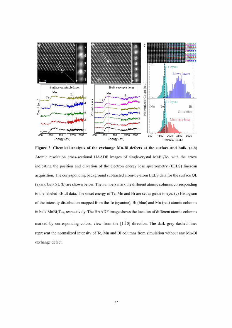
spectroscopy (EELS) across the reconstructed surface. Figure 2a shows EELS of each
atomic column in the surface QL structure, with the simultaneously collected HADDF

8
image shown on right. The identity of Bi shown by the M4 edge at 2688 eV only shows
up at the 2th and 4th layer, corresponding to the two brightest spots, which is consistent
to the expected STEM HAADF intensity due to its large atomic number. The atomic
EELS and simulated STEM HAADF image (see Fig. S5) suggested the surface QL is
alternating Te-Bi-Te-Bi-Te QL similar to the Bi2Te3 structure. However, it is surprising
that clear Mn signal, labelled by the L2,3 edge at 640 eV, also shows up exactly in the
Bi columns. This suggests that most of the Mn atoms doped into the Bi lattice column
given the high miscibility at the cation sites, i.e., antisite defects, BiMn or MnBi, may
present in the surface even before the surface collapse occurred.
To further confirm the scenario of BiMn or MnBi, we also collected atomic EELS
from the bulk SL structure. Figure 2b shows the EELS across the SL structure.
Surprisingly, we found clear Bi signal appeared in the Mn layer (4th atomic column in
Fig. 2b), while strong Mn signal at both the Bi layers (2nd and 6th layer), evidencing the
presence of BiMn and MnBi. As a result, the Mn layer has much brighter intensity than
the simulated STEM HAADF image which used the ideal SL model (Fig. S5), due to
the inclusion of the heavier Bi atoms, and vice versa. In contrast, Te layers show no Mn
or Bi signals, excluding the presence of other types of anti-site defects. However,
elemental distribution of a SL in the bulk is exactly 1:2:4 as probed by EDS, which
implied the occurrence of intralayer exchange between Bi and Mn atoms, resulting in
almost equal amount of BiMn and MnBi in both Mn and Bi layers. Since such Mn-Bi
intralayer exchange is omnipresent in the bulk, it played a key role in the surface
collapse and reconstruction process.
9
In order to further investigate the Mn-Bi intralayer exchange effect, we mapped
the intensity of all atomic columns in SL structure in a large scale using a peak intensity
finding software26 and performed quantitative statistical analysis. Figure 2c shows the
intensity histogram. Mn, Bi and Te sites are mapped separately, as indicated by the
markers shown on the representative STEM image. To quantitatively study the
intralayer exchange between the Mn and Bi layers, we compared the experimental value
to the simulations. The dark grey dashed lines in Fig. 2c are the simulated intensity of
Mn, Bi and Te columns using the ideal SL structure without any anti-site defects, where
the Te column is normalized to the experimental value for direct comparison. As
expected, intensity of all Mn column is much higher than the simulated one while Bi is
lower, both of which had wider distribution than Te, a direct evidence of intralayer Mn-
Bi intermixing. From the simulated intensity, when the concentration of BiMn reaches
30% in the Mn layer, the intensity of the Mn atomic column is almost similar to that of
Te (see Fig. S5c). Therefore, the average concentration of the anti-site defects in both
Mn and Bi layers can be qualitatively estimated by the full-with-half-maximum
(FWHM) of the intensity distribution with comparison to the simulation with different
concentration of Mn-Bi intermixing. The BiMn concentration in Mn-layer is found to be
40%~50%, which is approximately twice value of MnBi concentration in Bi atomic
layers. This is consistent with our previous analysis that the amount of BiMn and MnBi
should be equal due to the intralayer exchange, while Bi is double the amount of Mn
due to the 1:2:4 chemical stoichiometry.
10
Physical origin of the defect-triggered surface collapse and reconstruction
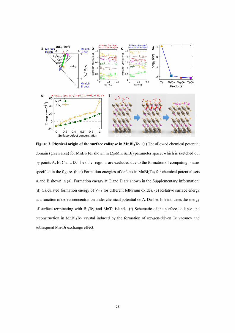
To uncover the physical origin of the as-observed surface reconstruction in
MnBi2Te4, we presented comprehensive thermodynamic defect calculations by using
density functional theory (DFT). By far, our experiments evidenced that high
concentration of intrinsic anti-site defects (BiMn and MnBi) are presented in the Mn and
Bi layers, thus we firstly examine the formation of anti-site defects due to the Bi-Mn
exchange in MnBi2Te4. Chemical potential substantially affects the calculations of
defect formation energy, therefore we determine the accessible range of the chemical
potential, i.e., growth condition, of MnBi2Te4 in (∆μMn, ∆μBi) parameter space with the
constraints imposed by competing binary compounds, as shown in the green area of Fig.
3a. In the unstable regions (white area), MnBi2Te4 tends to decompose to various
competing phases. Therefore, the formation energies of native defects are calculated
merely under two representative environments, i.e., Bi-rich condition (∆μBi ≈ 0 eV), and
Te-rich condition (∆μTe ≈ 0 eV) denoted by A and B points in Fig. 3a, respectively. More
information about defect calculations is provided in Supplementary Section Ⅲ to Ⅳ.
For Bi-rich condition (see Fig. 3b), BiMn, having the lowest formation energy, is
the dominant donor defect due to the excess valence electrons of Bi than Mn. On the
other hand, the cation-to-cation antisite defect (MnBi) has much lower formation energy
than the anion-to-cation antisite defect (TeBi) even in Te-rich condition (Fig. S7), thus
BiMn and MnBi are two dominant defects in MnBi2Te4. The combination of these two
antisite defects creates a double defect of Mn-Bi exchange (MnBi), with relatively small
formation energies shown in the dark-green line of Fig. 3b and 3c. This explained the

11
high concentration of the cation-to-cation antisite exchange defects observed in the
STEM cross-section image. Note that to form MnBi, no atoms exchange between
MnBi2Te4 and reservoirs is required.
The physical origin of ideal SL to the as-observed reconstructed surface (QL+DL
structure) should be closely related to the defect landscape of MnBi2Te4. Firstly, we
consider the total energy of MnBi2Te4 with MnBi exchange defects at the surface, and
compare with the total energy of Bi2Te3 and MnTe islands under surface reconstruction.
The latter is set to 0 as the reference, denoted by the dashed line in Fig. 3e. We find that
the energy of the defective SL surface increases monotonically with the increasing MnBi
concentration, which is consistent with its positive defect formation energy from our
calculation (see supplementary Section Ⅴ for calculation models and methods). To pass
the reference line and thus realize the collapse from SL to QL, the required
concentration of MnBi is extremely high (over 50%). Such a high defect concentration
is not observed in our experiments because the bulk still has stable SL framework
against reconstruction, only surface did. In other words, although MnBi is the dominant
defect under equilibrium growth condition, MnBi alone can hardly promote the SL
surface collapsed into QL. Therefore, the driving force of the surface collapse should
be something else, most likely some defects which may form at the surface regardless
of their relatively large formation energies in bulk.
From bulk to surface, the outermost layer (Te1 layer in MnBi2Te4) suffers the
strongest environmental perturbation, such as unintentionally introduced atomic
vacancies upon cleavage. It is known that tellurides like MnBi2Te4 is readily to be

12
oxidized, which would break the equilibrium growth condition. Taking tellurium oxides
into account, we reevaluate the formation energy of Te1 vacancy VTe1 (see
supplementary Section Ⅵ for calculation details). As illustrated in Fig. 3d, under
equilibrium Te-poor condition, the formation energy of VTe1 is about 1.1 eV, indicating
the relatively low VTe1 concentration in bulk. However, with the assistance of oxygen,
instead of forming elemental Te solid, Te forms tellurium oxides with VTe1 formation
energy decreased dramatically. We consider three tellurium oxides, TeO2, Te2O5 and
TeO3. For all cases, the calculated VTe1 formation energies are about −2 eV. The total
energy of MnBi2Te4 with VTe1 defects at the surface increases quickly with the
increasing of VTe1 concentration, as shown in Fig. 3e. To realize SL to QL collapse, the
required surface VTe1 concentration is about 20% in Bi-rich condition. With the
assistance of MnBi, the surface collapse may take place at an even lower VTe1
concentration. Overall, as illustrated in Fig. 3f, oxygen at the surface reacts with Te1
sublayer, leaving tellurium vacancies. Such surface VTe1 serves as the dominant driving
force to trigger the surface collapse and reconstruction in MnBi2Te4 by accelerating Bi-
Mn exchange. As a result, the residual Te and Mn atoms form MnTe islands covering
QL surface sparsely. This is indeed the case that we observed small amount of oxygen
signal at the interface between the QL structure and the graphite, as detected both by
EELS and EDS (see Fig. S4 and Fig. 1i), which confirmed the contribution of oxygen
in creating surface Te vacancies by forming oxides of tellurium. Moreover, the theory
also suggests that such surface reconstruction involve a kinetic thermal unequilibrium
process which would result in an incomplete Bi-Mn exchange, consistent of the

13
chemical stoichiometry of the QL and the amorphous/crystalline DL structure as probed
by EDS (See Fig1h and 1i).
Verifying the defect-induced surface collapse and reconstruction by in-situ STM
and STEM
To verify the scenario of the Te-vacancy-driven surface collapse suggested by
theory, we first tried to exclude the presence of oxygen by investigating in-situ cleaved
MnBi2Te4 surface using ultrahigh vacuum STM (operation pressure better than 2 x 10-
10 Torr), in which the oxygen concentration is multiple orders of magnitude lower than
the inert gas environment. Figure 4a shows the STM image of a freshly exfoliated
MnBi2Te4 single crystal terminating with the (00l) surface. Abrupt steps with uniform
height of ~1.4 nm (7 atomic layers, Fig. 4a) was obtained. Zoom-in STM image shows
an atomic crystalline surface (Fig.4b and 4c) with randomly distributed dark spots.
According to the bias-voltage-dependent STM images of these dark spots (see Fig. S9),
they are ascribed to the BiMn antisite defects underneath the Te layer, consistent with
our STEM results and the previous report27. This indeed confirmed that the ideal SL
MnBi2Te4 surface can be preserved in ultrahigh vacuum.
To introduce Te vacancies at the surface, an in-situ heating at 150 oC was then
applied to the surface for about 41 hours, since Te is easily sublimated at elevated
temperature. A clear structure collapse is observed, evidenced by the emergence of
holes with step height about 0.4 nm (2 atomic layers, Fig. 4d) inside the originally flat
surface (see Fig. 4e). As a result, the height of the collapsed region, as shown by the

14
dimmer contrast in Fig. 4e, is about 1 nm (the height profile in Fig. 4d), corresponding
to five atomic layers. The collapsed surface still shows similar atomic crystalline
structure with hexagonal patterns (Fig. 4h and 4g) due to the surface similarity between
MnBi2Te4 and Bi2Te3.
The above results are in agreement with the surface collapse and reconstruction
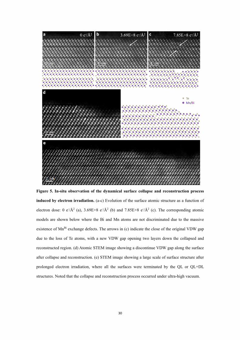
mechanism suggested by theory. We also attempted to directly capture the dynamical
process of the collapsed surface reconstruction. It is well-known that high energy
electron being used in imaging also simultaneously transfers momentum and energy to
the specimen which can result in beam-induced defects28. Figures 5a-5c show
sequential STEM images as a function of electron dose, highlighting the dynamical
surface collapse and reconstruction process in MnBi2Te4 surface. As the electron dose
accumulated, the atomic column intensity of the outermost layer (Te1 layer in QL
structure) is dimmed due to the loss of tellurium (Fig. 5b). Meanwhile, the gap between
the surface QL and the next SL, which is underneath the Te loss region as highlighted
by the arrow in Fig. 5b, narrowed down from 2.6 Å to 2 Å. A significant split is seen in
the first two atomic layers of the SL, a trend in separation into a DL and QL structure.
Finally, as the two outermost atomic columns are eliminated by electron bombardment,
the surface structure collapsed and reconstructed from a QL+SL to double QLs (Fig.
5c).
The dynamical collapse and reconstruction process indicate that the VDW gap can
close and reopen during the formation of defects depending on the exact layer
configurations. This indeed means that the VDW gap between layers can be

15
discontinued in a reconstructed surface as long as the outmost surface is a QL structure,
which is highlighted by the white arrows in Fig. 5d. Moreover, once Te vacancy was
formed, the ideal SL could not be the surface layer but only the QL did, due to the Te-
vacancy induced rapid exchange between the Mn/Bi layer, leaving a reconstructed DL
and QL as the outmost surface. This is evidenced in Fig. 5e, which shows a large view
of collapsed and reconstructed surface including QL+ SL, two QLs and DL + QL
structures, all of which manifested QL as the stable surface structures. The in-situ
dynamical imaging unambiguously confirmed that the formation of Te vacancy lead to
the surface collapse and reconstruction in MnBi2Te4 single crystal.
Discussion
Our results reveal that the surface structure of MnBi2Te4 is not as stable as
previously thought, a condition that inevitably affects the surface electronic structure
and thus the topological surface-bulk correspondence. Theoretically, when the surface
inherits the crystal and magnetic structures of the bulk, a gapped Dirac cone with dozens
of meV is expected due to the intrinsic magnetism. However, high-resolution ARPES
measurements unambiguously show a robust gapless Dirac cone at MnBi2Te4
surface16,23,24. One possibility is that the local moments of Mn atoms tends to distribute
randomly, giving rise to the almost zero band gap with linear dispersion. However,
direct experimental evidence, such as surface magnetic configurations, is still lacking
to support this hypothesis. Here, we suggest from our experimental results that the
surface collapse leads to significant absence of the magnetic atoms together with
16
magnetic disorder, resulting in the vanishing surface gap. First of all, with the surface
MnBi2Te4 SL collapsing to Bi2Te3 QL, the origin of the Dirac gap opening is mainly
the proximity effect from the ordered magnetic moments of the second topmost SL.
Compared with the perfect SL surface, the proximity-induced gap is much smaller. To
confirm this, we calculated by DFT the surface electronic structure with both
terminations, i.e., perfect MnBi2Te4 SL and collapsed Bi2Te3 QL. As shown in Fig. S10,
compared with the MnBi2Te4 termination without surface collapse and reconstruction,
the surface band gap of MnBi2Te4 with the surface layers degraded to Bi2Te3 shows a
significant reduction (from 42 meV to 5 meV). In addition, residual MnTe DL islands
on Bi2Te3 QL surface tend to be antiferromagnetic with parallel Mn spins in the basal
plane29,30. Therefore, the floating Mn atoms in the DL atoms cannot help to open the
surface Dirac gap either. Finally, our findings suggest that the device application of
thin-film MnBi2Te4, e.g., the quantum anomalous Hall effect, may also suffer the
impacts of surface collapse and reconstruction, which calls for further exploration.
Conclusion
In summary, we have discovered that a spontaneous surface collapse and
reconstruction in exfoliated MnBi2Te4 single-crystal occurs even under the protection
of a well-controlled inert gas environment. Combing STEM imaging, STM experiments
and DFT calculations, we systematically show such surface collapse resulted from the
synergistic effect of the high-concentrate intrinsic Mn-Bi exchange defects and the
formation of tellurium vacancy on the surface, which is induced by the trace of oxygen
in the inert gas environment. The surface reconstruction and the existence of massive

17
intrinsic defects bring a more comprehensive understanding of the antiferromagnetism
and the anomalous quantum states of MnBi2Te4 few-layer devices. The sensitive surface
also set a note on all MnBi2Te4 few-layer device fabricated in non-ultrahigh vacuum
environment, shed light in understanding the surface-related measurement of transport,
and exploration of exotic quantum phenomena and device fabrication for applications
based on MnBi2Te4 crystal.
Materials and Methods
1. Sample fabrication
The few-layer MnBi2Te4 was exfoliated from bulk MnBi2Te4 through a scotch-tap
method in a glove box filled with argon. The parent MnBi2Te4 bulk crystal is grown by
flux method16. The fresh surface is exposed in argon atmosphere, and subsequently
covered by graphite through a routine dry transfer method in the glove box to
encapsulate the surface from being oxidized. The cross-section STEM specimens were
quickly prepared using Focused Ion Beam after the sample was fetched from the glove
box, all of which ensured minimum surface degradation.
2. Characterizations
XRD - Single-crystal X-ray diffraction was performed on a Rigaku Miniex
diffractometer using Cu Kα radiation at room temperature.
XPS - The X-ray Photoelectron Spectroscopy measurement on the freshly exfoliated
surface of MnBi2Te4 crystal was performed on PHI 5000 Versaprobe Ⅲ. The spectrum
was analyzed by the PHI-MultiPak software.

18
AFM - Atomic Force Microscopy (AFM) measurement was carried out using the
Asylum Research, Cypher S system placed in an inert gas environment. To minimize
the oxidation of MnBi2Te4, the exfoliation of the MnBi2Te4 crystal and AFM
measurements are performed one after another in the same glove box.
STM - The STM experiments were carried out with a low-temperature STM
(UNISOKU Co., Ltd., USM1500) in ultrahigh vacuum (UHV) condition. The
MnBi2Te4 single crystal was cleaved along the (00l) crystal plane in the STM chamber
with a base pressure of 2×10⁻¹⁰ mbar. The freshly cleaved sample was immediately
transferred to the STM chamber for further measurements at 78 K (or 5K). The sample
was baked at 150 oC for 41 hours to introduce the surface reconstruction. The tungsten
tip was prepared by electrochemical etching and subsequent ebeam heating and Ar+
sputtering. We trained the tip apex on clean Cu (111) surface prior to all measurements.
STM topography images were processed by WSxM31.
STEM – STEM imaging, EDS and EELS analysis on MnBi2Te4 crystal were performed
on a FEI Titan Themis with a X-FEG electron gun and a DCOR aberration corrector
operating at 60 kV. The inner and outer collection angles for the STEM images (β1 and
β2) were 48 and 200 mrad, respectively. The convergence semi-angle of the probe is 25
mrad. The beam current was about 100 pA for high angle annular dark-field imaging,
the EDS and EELS chemical analyses. All imaging was performed at room temperature.
The quantitative element ratio of MnBi2Te4 crystal was confirmed by inductively
coupled plasma mass spectrometry (ICP-MS) analysis. The ratios between Mn, Bi and
Te were normalized based on the bulk MnBi2Te4 crystal. Thereinto, in the electronic

19
irradiation experiment, the electron dose (D) is calculated by D = I × T/A, using the
beam current (I), beam illuminating area (A), and the irradiation time (T).
3. Density Functional Theory Calculations
First-principles calculations were carried out using Vienna ab initio simulation
package (VASP)32 within the framework of density functional theory (DFT)33.
Exchange-correlation functional was described by the generalized gradient
approximation with the Perdew-Burke-Ernzerhof (PBE) formalism34. The electron-ion
interaction was treat by projector-augmented-wave (PAW) potentials35 with a
planewave-basis cuff of 500 eV. The whole Brillouin-zone was sampled by Monkhorst-
Pack grid36 for all models. Due to the correlation effects of 3d electrons in Mn atoms,
we employed GGA+U approach within the Dudarev scheme and set the U to be 5 eV,
which was investigated by and previous work16. All atoms were fully relaxed until the
force on each atom was less than 0.01 eV/Å and the total energy minimization was
performed with a tolerance of 10-5 eV. Freely available software VASPKIT37 was used
to deal with VASP output files. The calculation process is detailed in Supplementary
Section Ⅱ to Ⅵ.
Supporting Information
Supporting Information for this article is available in the online version of the paper.
Section S1. Characterization of the exfoliated surface of MnBi2Te4 crystal
Section S2. Stability of pure and Bi-doped MnTe double-layer
Section S3. Thermodynamic limits on the chemical potentials in DFT calculation
Section S4. Defect formation energy calculations
Section S5. Relative surface energy calculations
20
Section S6. Te1 vacancy formation energy with different final products
Section S7. STM images with different bias voltage
Section S8. Surface band structures of SL and QL terminations
Acknowledgements
We thank J. Zhang for the support of XPS measurement. The authors would like
to acknowledge the support from National Natural Science Foundation of China (Grant
No.11974156, 11874195 and 11674150), Guangdong International Science
Collaboration Project (Grant No. 2019A050510001 and 2017ZT07C062), National key
research and development program (Grant No. 2019YFA0704901), the Guangdong
Provincial Key Laboratory of Computational Science and Material Design (Grant No.
2019B030301001), the Key-Area Research and Development Program of Guangdong
Province (2019B010931001), Guangdong Innovative and Entrepreneurial Research
Team Program (Grant No. 2016ZT06D348) and also the assistance of SUSTech Core
Research Facilities, especially technical support from Pico-Centre that receives support
from Presidential fund and Development and Reform Commission of Shenzhen
Municipality. First-principles calculations were also supported by Center for
Computational Science and Engineering at SUSTech.
J.L. conceived the project. F.H. and J.L. made the TEM samples, performed AFM
measurement and STEM related experiments, analysis and simulations. DFT
calculations were done by Q.Y., H.S. and Q.L. Sample growth and X-ray analysis was
made by X.M., Y.H. and C.L. STM measurement was carried out by C.Z., X.W., Yu Z.
and Y.Z. J.L. constructed the schematic of MnBi2Te4 surface collapse and

21
reconstruction. M.H. participated in parts of STEM experiments. The work was
coordinated by J.L., Q.L. and Y.Z. The manuscript was written by J.L., F.H., Q.L. and
Q.Y. with input from all authors. All authors commented on the manuscript.
References
(1) Hasan, M. Z.; Kane, C. L. Colloquium: Topological Insulators. Rev. Mod. Phys.
2010, 82 (4), 3045–3067. https://doi.org/10.1103/RevModPhys.82.3045.
(2) Qi, X.-L.; Zhang, S.-C. Topological Insulators and Superconductors. Rev. Mod.
Phys. 2011, 83 (4), 1057–1110. https://doi.org/10.1103/RevModPhys.83.1057.
(3) Yu, R.; Zhang, W.; Zhang, H. J.; Zhang, S. C.; Dai, X.; Fang, Z. Quantized
Anomalous Hall Effect in Magnetic Topological Insulators. Science. 2010, 329
(5987), 61–64. https://doi.org/10.1126/science.1187485.
(4) Chang, C. Z.; Zhang, J.; Feng, X.; Shen, J.; Zhang, Z.; Guo, M.; Li, K.; Ou, Y.;
Wei, P.; Wang, L. L.; Ji, Z. Q.; Feng, Y.; Ji, S.; Chen, X.; Jia, J.; Dai, X.; Fang,
Z.; Zhang, S. C.; He, K.; Wang, Y.; Lu, L.; Ma, X. C.; Xue, Q. K. Experimental
Observation of the Quantum Anomalous Hall Effect in a Magnetic Topological
Insulator. Science. 2013, 340 (6129), 167–170.
https://doi.org/10.1126/science.1234414.
(5) Chang, C. Z.; Zhao, W.; Kim, D. Y.; Zhang, H.; Assaf, B. A.; Heiman, D.; Zhang,
S. C.; Liu, C.; Chan, M. H. W.; Moodera, J. S. High-Precision Realization of
Robust Quantum Anomalous Hall State in a Hard Ferromagnetic Topological
Insulator. Nat. Mater. 2015, 14 (5), 473–477. https://doi.org/10.1038/nmat4204.
(6) Soluyanov, A. A.; Gresch, D.; Wang, Z.; Wu, Q.; Troyer, M.; Dai, X.; Bernevig,
B. A. Type-II Weyl Semimetals. Nature 2015, 527 (7579), 495–498.
https://doi.org/10.1038/nature15768.
(7) Tang, P.; Zhou, Q.; Xu, G.; Zhang, S.-C. Dirac Fermions in an Antiferromagnetic
Semimetal. Nat. Phys. 2016, 12 (12), 1100–1104.
https://doi.org/10.1038/nphys3839.
(8) Mogi, M.; Kawamura, M.; Yoshimi, R.; Tsukazaki, A.; Kozuka, Y.; Shirakawa,
N.; Takahashi, K. S.; Kawasaki, M.; Tokura, Y. A Magnetic Heterostructure of
Topological Insulators as a Candidate for an Axion Insulator. Nat. Mater. 2017,
16 (5), 516–521. https://doi.org/10.1038/nmat4855.
(9) He, Q. L.; Pan, L.; Stern, A. L.; Burks, E. C.; Che, X.; Yin, G.; Wang, J.; Lian,
B.; Zhou, Q.; Choi, E. S.; Murata, K.; Kou, X.; Chen, Z.; Nie, T.; Shao, Q.; Fan,
Y.; Zhang, S.-C.; Liu, K.; Xia, J.; Wang, K. L. Chiral Majorana Fermion Modes
in a Quantum Anomalous Hall Insulator–Superconductor Structure. Science.
2017, 357 (6348), 294–299. https://doi.org/10.1126/science.aag2792.
(10) Tokura, Y.; Yasuda, K.; Tsukazaki, A. Magnetic Topological Insulators. Nat.
Rev. Phys. 2019, 1 (2), 126–143. https://doi.org/10.1038/s42254-018-0011-5.
22
(11) Li, J.; Li, Y.; Du, S.; Wang, Z.; Gu, B.-L.; Zhang, S.-C.; He, K.; Duan, W.; Xu,
Y. Intrinsic Magnetic Topological Insulators in van Der Waals Layered
MnBi2Te4-Family Materials. Sci. Adv. 2019, 5 (6), eaaw5685.
https://doi.org/10.1126/sciadv.aaw5685.
(12) Li, H.; Liu, S.; Liu, C.; Zhang, J.; Xu, Y.; Yu, R.; Wu, Y.; Zhang, Y.; Fan, S.
Antiferromagnetic Topological Insulator MnBi2Te4: Synthesis and Magnetic
Properties. 2019. http://arxiv.org/abs/1907.13018.
(13) Rienks, E. D. L.; Wimmer, S.; Sánchez-Barriga, J.; Caha, O.; Mandal, P. S.;
Růžička, J.; Ney, A.; Steiner, H.; Volobuev, V. V.; Groiss, H.; Albu, M.;
Kothleitner, G.; Michalička, J.; Khan, S. A.; Minár, J.; Ebert, H.; Bauer, G.;
Freyse, F.; Varykhalov, A.; Rader, O.; Springholz, G. Large Magnetic Gap at the
Dirac Point in Bi2Te3/MnBi2Te4 Heterostructures. Nature 2019, 576 (7787),
423–428. https://doi.org/10.1038/s41586-019-1826-7.
(14) Gong, Y.; Guo, J.; Li, J.; Zhu, K.; Liao, M.; Liu, X.; Zhang, Q.; Gu, L.; Tang,
L.; Feng, X.; Zhang, D.; Li, W.; Song, C.; Wang, L.; Yu, P.; Chen, X.; Wang,
Y.; Yao, H.; Duan, W.; Xu, Y.; Zhang, S.-C.; Ma, X.; Xue, Q.-K.; He, K.
Experimental Realization of an Intrinsic Magnetic Topological Insulator.
Chinese Phys. Lett. 2019, 36 (7), 076801. https://doi.org/10.1088/0256-
307X/36/7/076801.
(15) Liu, C.; Wang, Y.; Li, H.; Wu, Y.; Li, Y.; Li, J.; He, K.; Xu, Y.; Zhang, J.; Wang,
Y. Quantum Phase Transition from Axion Insulator to Chern Insulator in
MnBi2Te4. 2019. http://arxiv.org/abs/1905.00715.
(16) Hao, Y.-J.; Liu, P.; Feng, Y.; Ma, X.-M.; Schwier, E. F.; Arita, M.; Kumar, S.;
Hu, C.; Lu, R.; Zeng, M.; Wang, Y.; Hao, Z.; Sun, H.; Zhang, K.; Mei, J.; Ni, N.;
Wu, L.; Shimada, K.; Chen, C.; Liu, Q.; Liu, C. Gapless Surface Dirac Cone in
Antiferromagnetic Topological Insulator MnBi2Te4. Phys. Rev. X 2019, 9 (4),
041038. https://doi.org/10.1103/PhysRevX.9.041038.
(17) Ge, J.; Liu, Y.; Li, J.; Li, H.; Luo, T.; Wu, Y.; Xu, Y.; Wang, J. High-Chern-
Number and High-Temperature Quantum Hall Effect without Landau Levels.
2019, 1–21. http://arxiv.org/abs/1907.09947.
(18) Otrokov, M. M.; Rusinov, I. P.; Blanco-Rey, M.; Hoffmann, M.; Vyazovskaya,
A. Y.; Eremeev, S. V.; Ernst, A.; Echenique, P. M.; Arnau, A.; Chulkov, E. V.
Unique Thickness-Dependent Properties of the van Der Waals Interlayer
Antiferromagnet MnBi2Te4 Films. Phys. Rev. Lett. 2019, 122 (10), 107202.
https://doi.org/10.1103/PhysRevLett.122.107202.
(19) Otrokov, M. M.; Klimovskikh, I. I.; Bentmann, H.; Estyunin, D.; Zeugner, A.;
Aliev, Z. S.; Gaß, S.; Wolter, A. U. B.; Koroleva, A. V.; Shikin, A. M.; Blanco-
Rey, M.; Hoffmann, M.; Rusinov, I. P.; Vyazovskaya, A. Y.; Eremeev, S. V.;
Koroteev, Y. M.; Kuznetsov, V. M.; Freyse, F.; Sánchez-Barriga, J.;
Amiraslanov, I. R.; Babanly, M. B.; Mamedov, N. T.; Abdullayev, N. A.; Zverev,
V. N.; Alfonsov, A.; Kataev, V.; Büchner, B.; Schwier, E. F.; Kumar, S.; Kimura,
A.; Petaccia, L.; Di Santo, G.; Vidal, R. C.; Schatz, S.; Kißner, K.; Ünzelmann,
M.; Min, C. H.; Moser, S.; Peixoto, T. R. F.; Reinert, F.; Ernst, A.; Echenique,
P. M.; Isaeva, A.; Chulkov, E. V. Prediction and Observation of an
23
Antiferromagnetic Topological Insulator. Nature 2019, 576 (7787), 416–422.
https://doi.org/10.1038/s41586-019-1840-9.
(20) Mong, R. S. K.; Essin, A. M.; Moore, J. E. Antiferromagnetic Topological
Insulators. Phys. Rev. B 2010, 81 (24), 245209.
https://doi.org/10.1103/PhysRevB.81.245209.
(21) Zhang, D.; Shi, M.; Zhu, T.; Xing, D.; Zhang, H.; Wang, J. Topological Axion
States in the Magnetic Insulator MnBi2Te4 with the Quantized Magnetoelectric
Effect. Phys. Rev. Lett. 2019, 122 (20), 206401.
https://doi.org/10.1103/PhysRevLett.122.206401.
(22) Deng, Y.; Yu, Y.; Shi, M. Z.; Guo, Z.; Xu, Z.; Wang, J.; Chen, X. H.; Zhang, Y.
Quantum Anomalous Hall Effect in Intrinsic Magnetic Topological Insulator
MnBi 2 Te 4. Science. 2020, eaax8156. https://doi.org/10.1126/science.aax8156.
(23) Chen, Y. J.; Xu, L. X.; Li, J. H.; Li, Y. W.; Wang, H. Y.; Zhang, C. F.; Li, H.;
Wu, Y.; Liang, A. J.; Chen, C.; Jung, S. W.; Cacho, C.; Mao, Y. H.; Liu, S.;
Wang, M. X.; Guo, Y. F.; Xu, Y.; Liu, Z. K.; Yang, L. X.; Chen, Y. L.
Topological Electronic Structure and Its Temperature Evolution in
Antiferromagnetic Topological Insulator MnBi2Te4. Phys. Rev. X 2019, 9 (4),
041040. https://doi.org/10.1103/PhysRevX.9.041040.
(24) Li, H.; Gao, S.-Y.; Duan, S.-F.; Xu, Y.-F.; Zhu, K.-J.; Tian, S.-J.; Gao, J.-C.; Fan,
W.-H.; Rao, Z.-C.; Huang, J.-R.; Li, J.-J.; Yan, D.-Y.; Liu, Z.-T.; Liu, W.-L.;
Huang, Y.-B.; Li, Y.-L.; Liu, Y.; Zhang, G.-B.; Zhang, P.; Kondo, T.; Shin, S.;
Lei, H.-C.; Shi, Y.-G.; Zhang, W.-T.; Weng, H.-M.; Qian, T.; Ding, H. Dirac
Surface States in Intrinsic Magnetic Topological Insulators EuSn2As2 and
MnBi2nTe3n+1. Phys. Rev. X 2019, 9 (4), 041039.
https://doi.org/10.1103/PhysRevX.9.041039.
(25) Lin, J.; Zuluaga, S.; Yu, P.; Liu, Z.; Pantelides, S. T.; Suenaga, K. Novel Pd2Se3
Two-Dimensional Phase Driven by Interlayer Fusion in Layered PdSe2. Phys.
Rev. Lett. 2017, 119 (1), 016101.
https://doi.org/10.1103/PhysRevLett.119.016101.
(26) Zhang, Q.; Zhang, L. Y.; Jin, C. H.; Wang, Y. M.; Lin, F. CalAtom: A Software
for Quantitatively Analysing Atomic Columns in a Transmission Electron
Microscope Image. Ultramicroscopy 2019, 202 (January), 114–120.
https://doi.org/10.1016/j.ultramic.2019.04.007.
(27) Yan, J.-Q.; Zhang, Q.; Heitmann, T.; Huang, Z.; Chen, K. Y.; Cheng, J.-G.; Wu,
W.; Vaknin, D.; Sales, B. C.; McQueeney, R. J. Crystal Growth and Magnetic
Structure of MnBi2Te4. Phys. Rev. Mater. 2019, 3 (6), 064202.
https://doi.org/10.1103/PhysRevMaterials.3.064202.
(28) Hong, J.; Pan, Y.; Hu, Z.; Lv, D.; Jin, C.; Ji, W.; Yuan, J.; Zhang, Z. Direct
Imaging of Kinetic Pathways of Atomic Diffusion in Monolayer Molybdenum
Disulfide. Nano Lett. 2017, 17 (6), 3383–3390.
https://doi.org/10.1021/acs.nanolett.6b05342.
(29) Kriegner, D.; Výborný, K.; Olejník, K.; Reichlová, H.; Novák, V.; Marti, X.;
Gazquez, J.; Saidl, V.; Němec, P.; Volobuev, V. V.; Springholz, G.; Holý, V.;
Jungwirth, T. Multiple-Stable Anisotropic Magnetoresistance Memory in
24
Antiferromagnetic MnTe. Nat. Commun. 2016, 7 (1), 11623.
https://doi.org/10.1038/ncomms11623.
(30) He, Q. L.; Yin, G.; Grutter, A. J.; Pan, L.; Che, X.; Yu, G.; Gilbert, D. A.;
Disseler, S. M.; Liu, Y.; Shafer, P.; Zhang, B.; Wu, Y.; Kirby, B. J.; Arenholz,
E.; Lake, R. K.; Han, X.; Wang, K. L. Exchange-Biasing Topological Charges
by Antiferromagnetism. Nat. Commun. 2018, 9 (1), 2767.
https://doi.org/10.1038/s41467-018-05166-9.
(31) Horcas, I.; Fernández, R.; Gómez-Rodríguez, J. M.; Colchero, J.; Gómez-
Herrero, J.; Baro, A. M. WSXM: A Software for Scanning Probe Microscopy
and a Tool for Nanotechnology. Rev. Sci. Instrum. 2007, 78 (1), 013705.
https://doi.org/10.1063/1.2432410.
(32) Kresse, G.; Furthmüller, J. Efficient Iterative Schemes for Ab Initio Total-
Energy Calculations Using a Plane-Wave Basis Set. Phys. Rev. B 1996, 54 (16),
11169–11186. https://doi.org/10.1103/PhysRevB.54.11169.
(33) Chu, C. H.; Leung, C. W. The Convolution Equation of Choquet and Deny on
[IN]-Groups. Integr. Equations Oper. Theory 2001, 40 (4), 391–402.
https://doi.org/10.1007/BF01198136.
(34) Perdew, J. P.; Burke, K.; Ernzerhof, M. Generalized Gradient Approximation
Made Simple. Phys. Rev. Lett. 1996, 77 (18), 3865–3868.
https://doi.org/10.1103/PhysRevLett.77.3865.
(35) Joubert, D. From Ultrasoft Pseudopotentials to the Projector Augmented-Wave
Method. Phys. Rev. B - Condens. Matter Mater. Phys. 1999, 59 (3), 1758–1775.
https://doi.org/10.1103/PhysRevB.59.1758.
(36) Pack, J. D.; Monkhorst, H. J. “special Points for Brillouin-Zone Integrations”-a
Reply. Phys. Rev. B 1977, 16 (4), 1748–1749.
https://doi.org/10.1103/PhysRevB.16.1748.
(37) Wang, V.; Xu, N.; Liu, J. C.; Tang, G.; Geng, W.-T. VASPKIT: A Pre- and Post-
Processing Program for VASP Code. 2019, 1–14.
http://arxiv.org/abs/1908.08269.

25
Figures
Figure 1 Atomic characterizations of the MnBi2Te4 surface structure. (a) X-ray diffraction
(XRD) pattern (red), and the referenced (00l) peaks (blue) from standard PDF file of the parent
single MnBi2Te4 crystal. (b) Large-scale high-angle annular dark field scanning transmission
electron microscopy (HAADF-STEM) image of the cross section of layered MnBi2Te4 crystal
viewed along the [110] direction, with the overlaid graphite as surface protection. (c-e) Zoom-in
atomic resolution HAADF-STEM images of the surface and bulk highlighted in (b), respectively. A

26
quintuple-layer (QL) with double-layer (DL) crystalline/amorphous structure, instead of the ideal
septuple-layer (SL) MnBi2Te4, is seen at the surface. The arrows highlight the crystalline DL islands
on the surface. (d) and (f) are the corresponding atomic models from the images, respectively. (g) A
large scale of the atomic structure of the MnBi2Te4 surface showing the omnipresent crystalline DL
islands indicated by arrows. (h, i) The corresponding energy dispersive spectrum (EDS) maps for
the surface QL and DL crystalline/amorphous structure, respectively. Cu and C come from the grid
and substrate.
27
Figure 2. Chemical analysis of the exchange Mn-Bi defects at the surface and bulk. (a-b)
Atomic resolution cross-sectional HAADF images of single-crystal MnBi2Te4 with the arrow
indicating the position and direction of the electron energy loss spectrometry (EELS) linescan
acquisition. The corresponding background subtracted atom-by-atom EELS data for the surface QL
(a) and bulk SL (b) are shown below. The numbers mark the different atomic columns corresponding
to the labeled EELS data. The onset energy of Te, Mn and Bi are set as guide to eye. (c) Histogram
of the intensity distribution mapped from the Te (cyanine), Bi (blue) and Mn (red) atomic columns
in bulk MnBi2Te4, respectively. The HAADF image shows the location of different atomic columns
marked by corresponding colors, view from the [1 1 0] direction. The dark grey dashed lines
represent the normalized intensity of Te, Mn and Bi columns from simulation without any Mn-Bi
exchange defect.
28
Figure 3. Physical origin of the surface collapse in MnBi2Te4. (a) The allowed chemical potential
domain (green area) for MnBi2Te4 shown in (∆μMn, ∆μBi) parameter space, which is sketched out
by points A, B, C and D. The other regions are excluded due to the formation of competing phases
specified in the figure. (b, c) Formation energies of defects in MnBi2Te4 for chemical potential sets
A and B shown in (a). Formation energy at C and D are shown in the Supplementary Information.
(d) Calculated formation energy of VTe1 for different tellurium oxides. (e) Relative surface energy
as a function of defect concentration under chemical potential set A. Dashed line indicates the energy
of surface terminating with Bi2Te3 and MnTe islands. (f) Schematic of the surface collapse and
reconstruction in MnBi2Te4 crystal induced by the formation of oxygen-driven Te vacancy and
subsequent Mn-Bi exchange effect.

29
Figure 4. In-situ heating of the exfoliated MnBi2Te4 surface in ultrahigh vacuum. (a) Large-
scale STM image of MnBi2Te4 (00l) surface exfoliated in ultrahigh vacuum and the corresponding
height line profile along the blue line. (b) Zoom-in STM image of the MnBi2Te4 (00l) surface with
defects. (c) Atomic-resolution image of the MnBi2Te4 surface. The dark spots are concluded as the
BiMn anti-site defects under the Te layer. The SL height and the crystalline surface imply the intact
MnBi2Te4 surface can be preserved in ultrahigh vacuum. (d) Large-scale STM image of the in-situ
heated MnBi2Te4 surface and the corresponding height line profile along the blue line. Holes with
DL heights appear after heating. (e) Zoom-in image of the annealed surface. (f, g) Atomically
resolved STM images of the annealed surface marked by black and green box in (e), respectively.
Tunneling Parameters: (a) Vbias = 1V, It = 200 pA (b) Vbias = 1V, It =50 pA (c) Vbias = -1 V, It = 3 nA
(d) Vbias = 1.2 V, It = 20 pA (e) Vbias = 1.5 V, It = 1 nA (f) Vbias = -1 V, It = 1 nA (g) Vbias = 0.2 V, It =
500 pA.
30
Figure 5. In-situ observation of the dynamical surface collapse and reconstruction process
induced by electron irradiation. (a-c) Evolution of the surface atomic structure as a function of
electron dose: 0 e-/Å2 (a), 3.69E+8 e-/Å2 (b) and 7.85E+8 e-/Å2 (c). The corresponding atomic
models are shown below where the Bi and Mn atoms are not discriminated due to the massive
existence of MnBi exchange defects. The arrows in (c) indicate the close of the original VDW gap
due to the loss of Te atoms, with a new VDW gap opening two layers down the collapsed and
reconstructed region. (d) Atomic STEM image showing a discontinue VDW gap along the surface
after collapse and reconstruction. (e) STEM image showing a large scale of surface structure after
prolonged electron irradiation, where all the surfaces were terminated by the QL or QL+DL
structures. Noted that the collapse and reconstruction process occurred under ultra-high vacuum.

31
Supporting Information
Section Ⅰ. Characterization of the exfoliated surface of MnBi2Te4 crystal ...................................... 32
Section Ⅱ. Stability of pure and Bi-doped MnTe double-layer ....................................................... 35
Section Ⅲ. Thermodynamic limits on the chemical potentials in DFT calculation ........................ 36
Section Ⅳ. Defect formation energy calculations .......................................................................... 36
Section Ⅴ. Relative surface energy calculations ............................................................................. 37
Section Ⅵ. Te1 vacancy formation energy with different final products ....................................... 38
Section Ⅶ. STM images with different bias voltage ..................................................................... 38
Section Ⅷ. Band structures of slabs with SL and QL terminations ............................................. 39
References ....................................................................................................................................... 40
32
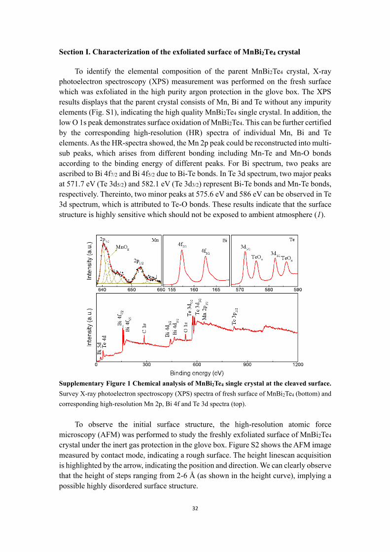
Section Ⅰ. Characterization of the exfoliated surface of MnBi2Te4 crystal
To identify the elemental composition of the parent MnBi2Te4 crystal, X-ray
photoelectron spectroscopy (XPS) measurement was performed on the fresh surface
which was exfoliated in the high purity argon protection in the glove box. The XPS
results displays that the parent crystal consists of Mn, Bi and Te without any impurity
elements (Fig. S1), indicating the high quality MnBi2Te4 single crystal. In addition, the
low O 1s peak demonstrates surface oxidation of MnBi2Te4. This can be further certified
by the corresponding high-resolution (HR) spectra of individual Mn, Bi and Te
elements. As the HR-spectra showed, the Mn 2p peak could be reconstructed into multi-
sub peaks, which arises from different bonding including Mn-Te and Mn-O bonds
according to the binding energy of different peaks. For Bi spectrum, two peaks are
ascribed to Bi 4f7/2 and Bi 4f5/2 due to Bi-Te bonds. In Te 3d spectrum, two major peaks
at 571.7 eV (Te 3d5/2) and 582.1 eV (Te 3d3/2) represent Bi-Te bonds and Mn-Te bonds,
respectively. Thereinto, two minor peaks at 575.6 eV and 586 eV can be observed in Te
3d spectrum, which is attributed to Te-O bonds. These results indicate that the surface
structure is highly sensitive which should not be exposed to ambient atmosphere (1).
Supplementary Figure 1 Chemical analysis of MnBi2Te4 single crystal at the cleaved surface.
Survey X-ray photoelectron spectroscopy (XPS) spectra of fresh surface of MnBi2Te4 (bottom) and
corresponding high-resolution Mn 2p, Bi 4f and Te 3d spectra (top).
To observe the initial surface structure, the high-resolution atomic force
microscopy (AFM) was performed to study the freshly exfoliated surface of MnBi2Te4
crystal under the inert gas protection in the glove box. Figure S2 shows the AFM image
measured by contact mode, indicating a rough surface. The height linescan acquisition
is highlighted by the arrow, indicating the position and direction. We can clearly observe
that the height of steps ranging from 2-6 Å (as shown in the height curve), implying a
possible highly disordered surface structure.

33
Supplementary Figure 2 Characterization of the cleaved surface morphology. Atomic Force
Microscopy (AFM) image on the fresh cleaved surface of MnBi2Te4 crystal with the arrow
indicating the position and direction of the height linescan acquisition.
To quantitative identify the chemical composition, we studied the energy
dispersive spectrum (EDS) of the bulk MnBi2Te4 crystal, which below the surface,
highlighted by the red dashed rectangle in Fig. S3a. The quantitative EDS mapping
verifies the bulk is MnBi2Te4 single crystal, with estimated ratio of Mn, Bi and Te as ~
1:2:4 in the septuple-layer structure (see Fig. S3b). In addition, the EDS elemental maps
for individual elements of Mn, Bi and Te indicate that manganese mainly distributes in
the middle of septuple layer in the corresponding STEM image, bismuth and tellurium
elements mainly distribute on the corresponding stacking layers in bulk SLs as shown
in Fig. S3c.
Supplementary Figure 3 Chemical analysis of MnBi2Te4 single crystal at surface and bulk. (a)
HAADF image of atomic structure of single MnBi2Te4 at cross section of surface, taken from the
[1Ῑ0] direction. (b) The energy dispersive spectrum (EDS) from the highlighted zone by the red
dashed rectangle in (a). Cu and C come from the grid and substrate, respectively. (c) The

34
corresponding EDS maps for individual elements of Mn, Bi and Te.
Supplementary Figure 4 Chemical analysis of the cleaved surface with the protection using
graphite. (a) HAADF image of atomic structure of single MnBi2Te4, (b) corresponding EELS maps
for individual area from (a), confirming the position of MnBi2Te4 and Graphite.
Supplementary Figure 5 The intensity variation in STEM image with different concentration
of exchange Mn-Bi defects. (a-b) Line intensity profiles along the highlighted blue (experiment)
and red (simulation using the ideal models) dashed lines in the corresponding images, indicating the
intensity of each atomic columns in the surface quintuple-layer (a) and bulk septuple-layer (b). (c)
Line intensity profiles along the MnBi2Te4 septuple-layer with different Bi-Mn anti-site defect
concentrations. Red (0%), blue (30%), green (50%) and dark (70%) dashed lines highlighted the
intensity of each atomic columns with different Bi-Mn exchange defects in the simulation.
In order to verify the composition of the double crystalline/amorphous layer
35
(called DL-region) on the exfoliated surface of MnBi2Te4 crystal, we collected the
EELS from different region of the surface, including QL region, DL-region and the
region above DL-region as shown in Fig. S4. Obviously, the graphite is above the DL-
region according to the abrupt enhancement of C signal in C-area compared to A- and
B-area. The QL has slight Mn with almost invisible Mn signal in A-area, which is
consistent with the EDS results (Fig. 1h). In the B-area, we found clear Mn, Te and
some O signals. Slight Mn and Te signal are observed in graphite region presumably
due to the sputtering during FIB sample preparation.
The atom-by-atom EELS confirmed the existence of MnBi anti-site exchange
defects in bulk SL structure. To quantify the defects concentration, simulation was
carried out using models with different concentration of MnBi anti-site exchange defects.
Figure S5 shows the intensity of each atomic column along the SL structure as
highlighted dashed lines. We found discrepancy between experiment and simulation in
the bulk MnBi2Te4 crystal, especially for the Mn atomic layer in the SL structure as
shown in Fig. S5b. The simulation results display a very low Z-contrast of Mn layer,
however the intensity is higher than the Te layer in experiment. Combined with the
EELS results in Fig. 2b, it can be proved that the middle layer of SL has a large number
of BiMn anti-site defects. To quantify the concentration of anti-site defect in experiment,
we performed the simulation on the SL MnBi2Te4 single crystal with a series of BiMn
anti-site defects concentration. The simulation results display that the intensity of Mn
layer is equal to the Te layer as the BiMn anti-site defects concentration reaches 30%
(see Fig. S5c). Therefore, we can estimate concentration of anti-site defects in
MnBi2Te4 crystal based on their intensity.
Section Ⅱ. Stability of pure and Bi-doped MnTe double-layer
Supplementary Figure 6 The calculations on the stability of MnTe DL. Phonon dispersion of
MnTe DL.
Phonon dispersion calculations were carried out to study the stability of pure and
Bi-doped MnTe double-layer (DL). Here, open source package Phonopy(2) was used
for phonon calculations with forces obtained from Vienna ab initio simulation package
36
(VASP)(3) by finite displacement method. As shown in Fig. S6, phonon dispersion of
MnTe DL contains sizable imaginary eigenfrequencies through symmetry lines, which
indicates that MnTe DL is dynamically unstable. On the other hand, Bi-doped MnTe
DL (Bi:Mn:Te = 0.22:0.78:1) underwent dramatically structure deformation during
optimization. Such significant reconstruction indicates that the supposed Bi-doped
MnTe in DL framework is energetically rather unstable.
Section Ⅲ. Thermodynamic limits on the chemical potentials in DFT calculation
We determine the allowed chemical region with restrictions below, followed by
the approach proposed in previous reports(4, 5).
(ⅰ) To maintain a stable MnBi2Te4 compound, the sum of chemical potentials of its
constituent atoms must equal the formation enthalpy of the compound. That is
∆μMn + 2∆μBi + 4∆μTe = ∆H(MnBi2Te4) (1)
(ⅱ) In addition to eq. (1), to avoid solid/gas elemental precipitation, we need
∆μMn ≤ 0, ∆μBi ≤ 0, ∆μTe ≤ 0, (2)
Combination of eq. (1) and eq. (2) sketch out the entire chemical potential domain.
(ⅲ) Constraints are also imposed by other possible competing phases. For example, to
avoid forming Bi2Te3, we need
2∆μBi + 3∆μTe ≤ ∆H(Bi2Te3) (3).
Here, we consider as competing phases Bi4Te3, Bi8Te9, Bi2Te3, MnTe and MnTe2. The
resulting accessible region of the chemical potentials is illustrated in Fig. 3a in (∆μMn,
∆μBi) plane.
Section Ⅳ. Defect formation energy calculations
The formation energy of a defect α in charge state q is defined as(6, 7)
H(αq) = E(αq) – E(host) − iii μn + q(EF + host
VBMε ) + Ecorr. (4)
Where E(host) is the energy of the pure host supercell, and E(αq) is the total energy of
defective structure using an equivalent supercell. The integer ni indicates the number of
atoms of type i (host atoms or impurity atoms) that have been added to (ni > 0) or
removed from (ni < 0) the supercell to form the defect, and the μi are the corresponding
chemical potentials of these species. EF ranges from 0 to bulk bandgap. host
VBMε is the
valence band maximum eigenvalue of the host. Finally, Ecorr. is a correction term
account for finite-size effects(8–10). In this work, we calculate the correction energy
with the freely available SXDEFECTALIGN code(10). Based on A, B, C and D sets of
chemical potentials shown in Fig. 3a, we calculate typical native defect formation
energies, as shown in Fig. S7. Note that, under all equilibrium growth conditions, BiMn
remains the dominant defect with negative formation energy. In fact, all allowed growth
conditions impose ∆μMn < −1 eV, which means Mn rather poor condition. Mn sublattice
is readily to be occupied by Bi or Te atoms. However, formation energy of TeMn is larger
than that of BiMn by more than 1 eV even in Te rich condition. Taking this into account,
for all growth conditions, BiMn is the dominant defect in MnBi2Te4, which may not easy

37
to be ruled out by manipulating growth condition.
Supplementary Figure 7 DFT calculations on the formation energies of various defects.
Formation energies of defects in MnBi2Te4 for chemical potential sets A, B, C and D shown in Fig.
3a.
Section Ⅴ. Relative surface energy calculations
To simulate MnBi2Te4 surface, we construct slab model contains two Te1-Bi-Te2-
Mn-Te2-Bi-Te1 septuple layer (SL). One SL is fixed while the other one is relaxed. To
decouple the interaction between neighboring slabs, a 15 Å thick vacuum layer was
added to the slab along the c direction. As the reference, we set energy of slab with
surface terminating by Bi2Te3 and islands MnTe to 0 (dash line in Fig. S8). For slab
with surface terminating by SL framework including defect, the energy is calculated by
energy of slab with defective surface plus total chemical potentials of defect atoms. For
example, considering surface including xVTe1, its energy is defined as
E( 1TexV
T-SLslab ) + xμTe1 (5)
Where E( 1TexV
T-SLslab ) is energy of slab terminating by SL containing xVTe1.
The relative surface energy is then obtained by
E( 1TexV
T-SLslab ) + xμTe1 – E(32TeBiTslab − ) – E(MnTe) (6)
Where E(32TeBiTslab − ) is energy of slab terminating by Bi2Te3 layer. E(MnTe) is energy
of bulk MnTe. The calculated relative surface energy for points A, B, C and D in Fig.
3a are shown in Fig. S8.

38
Supplementary Figure 8 DFT calculations on relative surface energy. Relative surface energy
as a function of defect concentration under chemical potential set A, B, C and D shown in Fig. 3a.
Section Ⅵ. Te1 vacancy formation energy with different final products
For different final products, VTe1 formation energies are calculated by
E(defect) + m
1μTemOn – E(host) −
m
n
2μO2 (7)
Where E(defect) is energy of supercell including one VTe1. E(host) is energy of perfect
equivalent supercell. μTemOn is chemical potential of tellurium oxide TemOn. μO2 is
chemical potential of oxygen.
Section Ⅶ. STM images with different bias voltage
From the STM images (Fig. 5), we can observe massive defects on the cleaved
surface of MnBi2Te4 single crystal. A series of bias voltage was applied to examine the
defects (see Fig. S9). The images were taken at the same location with identical
tunneling current of 0.5 nA. As bias voltage changes from positive to negative, the dark
spots remain their contrast, changing from triangularly located dots to blurred dark spot,
similar to the previous reported BiMn anti-site defects in Mn doped Bi2Te3 crystal.

39
Supplementary Figure 9 In-situ characterizations of the cleaved surface morphology. Sample-
bias-dependent STM topographs of the freshly cleaved MnBi2Te4 (00l) surface.
Section Ⅷ. Band structures of slabs with SL and QL terminations
Supplementary Figure 10 DFT calculated surface band structures of MnBi2Te4 SL and Bi2Te3
QL terminations. a. Calculated band structure of an 8-SL slab. b. Calculated band structure of a
slab composed of 6 SLs sandwiched by 2 QLs. Te 5p and Bi 6p states are indicated by blue and red
points, respectively. Slabs models are schematized by the bottom right rectangles. An A-type AFM
spin configuration is used in our simulations, as indicated by the black arrows in the rectangles.

40
References
1. H. Li, S. Liu, C. Liu, J. Zhang, Y. Xu, R. Yu, Y. Wu, Y. Zhang, S. Fan,
Antiferromagnetic Topological Insulator MnBi2Te4: Synthesis and Magnetic
properties (2019) (available at http://arxiv.org/abs/1907.13018).
2. A. Togo, I. Tanaka, First principles phonon calculations in materials science. Scr.
Mater. 108, 1–5 (2015).
3. G. Kresse, J. Furthmüller, Efficient iterative schemes for ab initio total-energy
calculations using a plane-wave basis set. Phys. Rev. B. 54, 11169–11186 (1996).
4. C. Persson, Y.-J. Zhao, S. Lany, A. Zunger, n-type doping of CuInSe2 and
CuGaSe2. Phys. Rev. B. 72, 035211 (2005).
5. A. Walsh, Y. Yan, M. M. Al-Jassim, S. H. Wei, Electronic, energetic, and
chemical effects of intrinsic defects and Fe-doping of CoAl2O4: A DFT+U study.
J. Phys. Chem. C. 112, 12044–12050 (2008).
6. S. B. Zhang, J. E. Northrup, Chemical Potential Dependence of Defect
Formation Energies in. Phys. Rev. Lett. 67, 2339–2342 (1991).
7. C. G. Van De Walle, D. B. Laks, G. F. Neumark, S. T. Pantelides, First-
principles calculations of solubilities and doping limits: Li, Na, and N in ZnSe.
Phys. Rev. B. 47, 9425–9434 (1993).
8. G. Makov, M. C. Payne, Periodic boundary conditions in ab initio calculations.
Phys. Rev. B. 51, 4014–4022 (1995).
9. S. Lany, A. Zunger, Assessment of correction methods for the band-gap problem
and for finite-size effects in supercell defect calculations: Case studies for ZnO
and GaAs. Phys. Rev. B. 78, 235104 (2008).
10. C. Freysoldt, J. Neugebauer, C. G. Van de Walle, Fully Ab Initio Finite-Size
Corrections for Charged-Defect Supercell Calculations. Phys. Rev. Lett. 102,
016402 (2009).