Loxyde de Zinc ZnO 5 décembre 2006 Morphogenèse Chimique Jacques Livage.

Residual Stress Relaxation and Microstructure in ZnO Thin Films
Istem Ozena and Mehmet Ali Gulgunb
Sabanci University, Faculty of Engineering and Natural Sciences,
34956, Orhanli, Tuzla, Istanbul, Turkey. [email protected]
Keywords: ZnO, thin films, residual stress, microstructure, annealing, aging. Abstract: Stability under normal environmental conditions over a long period of time is crucial for sustainable thin-film device performance. Pure ZnO films with thicknesses in the 140 - 450 nm range were deposited on amorphous glass microscope slides and (100)-oriented single crystal silicon wafers by radio frequency magnetron sputtering. The depositions were performed at a starting temperature of 200 oC. ZnO films had a columnar microstructure strongly textured along the <0002> direction. XRD peak-shift analysis revealed that the films were under residual, compressive, in-plane stress of -5.46 GPa for the glass substrate and -6.69 GPa for the Si substrate. These residual stresses could be completely relaxed by thermal annealing in air.
When left under normal environmental condition over an extended period of time the films failed under buckling leading to extensive cracking of the films. The XRD and SEM results indicated different mechanisms of stress relaxation that were favored in the ZnO thin films depending on the energy provided. Although thermal annealing eliminated residual stresses, serious micro-structural damage upon annealing was observed. Thermal annealing also led to preferential growth of some ZnO crystals in the films. This kind of behavior is believed to be indicative of stress-induced directional diffusion of ZnO. It appears that for the extended stability of the films, the stresses have to be eliminated during deposition. Introduction In this study, the decay of the residual stresses and the microstructure of sputtered ZnO thin films were investigated. ZnO is a wide band-gap (3.17 eV) semi-conducting oxide with wide-ranging potential applications in the fields of electronics and optics. The electrical, optical, magnetic etc. properties of ZnO films are known to be affected by the residual stresses in the films [1-3]. In these studies, textured growth of ZnO deposited by radio frequency magnetron sputtering and the residual compressive stresses in the films had been reported and the stresses were released by annealing, possibly due to improved homogeneity and/or the out-diffusion of trapped oxygen or argon [1-3].
Mechanical properties of ZnO thin films such as adhesion, stability towards delamination etc. are not investigated in detail in literature, although they are very important for stable device performance. Residual stresses are known to exist in thin films regardless of the type of deposition method and could be calculated by several direct or indirect methods. The stresses in metallic thin film are investigated in detail; however, the mechanisms leading to the formation and relaxation of these stresses are not fully understood for ceramic materials [4-7]. There are many factors proposed to be playing a role in the creation of these stresses, e.g. thermal expansion mismatch of the film and the substrate material, atom incorporation into the growing film during deposition, lattice misfit with the substrate, variation of inter-atomic spacing with crystal size, recrystallization processes, microscopic voids, and phase transformations [4, 5]. Moreover, the nature and magnitude of these stresses vary with the deposition method and post-deposition treatments.
Another complication is that the residual stresses in thin films are dynamic: they change over time with accompanying changes in the microstructure of the film [7]. Possible mechanisms include
Advances in Science and Technology Vol. 45 (2006) pp. 1316-1321online at http://www.scientific.net© (2006) Trans Tech Publications, Switzerland
All rights reserved. No part of contents of this paper may be reproduced or transmitted in any form or by any means without thewritten permission of the publisher: Trans Tech Publications Ltd, Switzerland, www.ttp.net. (ID: 212.98.201.1-19/12/06,13:06:49)

recrystallization within the film, micro-structural variations in the film-substrate interface or other phase transformations. If the amount of mechanical energy stored inside the film is considerably large (several GPa), it may further be released by crack generation, crack propagation and peeling of the layer from the substrate. Stability under normal environmental conditions over time, thus investigation of stress dynamics, is crucial for sustainable thin-film device performance.
Our previous results showed that the amount of residual stresses depends on the substrate type and the substrate temperature [8]. After prolonged storage of the thin film samples under ambient conditions, the films cracked and delaminated from the substrate [9]. On the other hand, upon thermal annealing, damage in the microstructure of the film-substrate interface layer was observed. The origin of the residual stresses as well as the stress relaxation mechanisms in ZnO thin films is still under investigation. Experimental Procedure
ZnO films were deposited by radio frequency magnetron sputtering (Teknoplazma, Turkey). Pure (99.999 %) ZnO was used as the sputtering target. Glass microscope cover slides and (100) oriented Si wafer pieces were used as substrates. The initial substrate temperature was 200 oC and the deposition was performed under cooling environment and the final temperature was 65 oC. The other deposition parameters and the procedure was as published in our previous work [8]. The sample list with the post-deposition treatments is summarized in Table 1.
Following film deposition, some samples were thermally annealed in air at 600 oC for 6 hours. Crystalline phases were examined by XRD. The reflection angle (2�) was varied continuously from 10° to 90° in locked-couple mode with a step size of 0.02 °/step and 0.5 s/step. Film thickness and microstructure were monitored by scanning electron microscope (SEM; Zeiss, Germany). The XRD and SEM analysis of both the as-deposited and the thermally annealed films were repeated 28 months later to investigate the effects of aging on the stresses and the microstructure of the films. The residual stresses were calculated from the strains measured from the XRD peak positions by the biaxial strain model [10]. Table 1. Samples and preparation parameters.
Sample no Substrate Post-deposition treatment G-0 Glass - G-1 Glass Thermal annealing G-2 Glass Aging S-0 Si - S-1 Si Thermal annealing S-2 Si Aging
Results
Nano-crystalline ZnO films grew with a columnar microstructure on both glass and Si
substrates. The grain sizes were calculated by Scherrer’s formula [11] from the full width-half maximum (FWHM) values of the (0002) diffraction peaks and the results are given in Table 2. XRD measurements revealed that the films are highly textured along the c-axis, giving a single diffraction peak from the ZnO (0002) plane. For all of the films grown on different substrates under various conditions, the shift in the (0002) peak position as compared to the one from a stress-free powder specimen indicated that these films were under residual planar compressive stress (Fig. 1a). The stress values for various samples are given in Table 2. Compressive, in-plane residual stresses were found to be -5.46 GPa for the ZnO film on glass substrate and -6.69 GPa for the case of the Si
11th International Ceramics Congress1317

(100) substrate. Thermal annealing reduced the compressive stresses to stress-free state. The (0002) peaks of both the aged and the annealed samples were narrower and more symmetrical than those of the as-deposited samples, indicating improved crystallinity and grain growth accompanying stress-release. Parallel results were seen upon prolonged aging as well (Fig. 1b and 1c).
(a) (b) (c) Figure 1. Shift of the (0002) peak of ZnO indicating residual stresses. The data shows the effect of a) substrate material, b) aging and annealing of ZnO on the glass substrate, c) aging and annealing on the Si(100) substrate. The vertical line represents the position of the (0002) peak in stress-free ZnO powder. The (0002) peaks of ZnO on samples G-2 and S-2 are scaled with those of G-0 and S-0 for comparison.
Table 2. Residual stresses and FWHM value depending on substrate type, substrate temperature, thermal annealing, and aging.
Sample no FWHM [2θθθθ °]
Grain size [nm]
Residual stress, σσσσ [GPa]
Error range of stress, ∆∆∆∆σσσσ [GPa]
G-0 0.347 23.9 -5.46 ±0.26 G-1 0.293 28.4 -0.57 ±0.26 G-2 0.266 31.3 -1.25 +0.73 /-0.66 S-0 0.928 8.9 -6.69 ±0.26 S-1 0.357 23.3 -0.48 ±0.26 S-2 0.378 22.0 -0.31 +0.73 /-0.66
SEM analysis revealed that there were simultaneous changes in the microstructure as the
stresses were released. Upon prolonged aging, local loss of adhesion was observed in the films (Fig. 2a). Upon further annealing of these samples, crack propagation and delamination of the film from the substrate was observed (Fig. 2b). A closer examination of the films reveals the formation of porosity at the surface upon annealing (Fig. 3a) and consequent formation of elongated crack-like defects upon pore coalescence (Fig. 4). Similar pore formation upon annealing was observed at the cross-sectional views of the films as well (Fig. 3b). Another consequence of annealing was the growth of ZnO crystals on the film surface (Fig. 5). Such directional growth of few crystals is believed to be indicative of stress-induced diffusion of ZnO within the film.
Advances in Science and Technology Vol. 45 1318
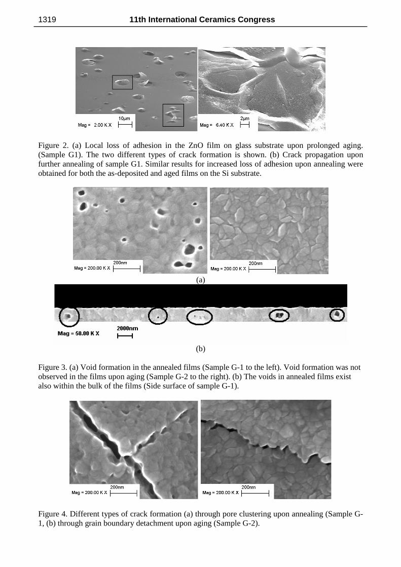
Figure 2. (a) Local loss of adhesion in the ZnO film on glass substrate upon prolonged aging. (Sample G1). The two different types of crack formation is shown. (b) Crack propagation upon further annealing of sample G1. Similar results for increased loss of adhesion upon annealing were obtained for both the as-deposited and aged films on the Si substrate.
(a)
(b)
Figure 3. (a) Void formation in the annealed films (Sample G-1 to the left). Void formation was not observed in the films upon aging (Sample G-2 to the right). (b) The voids in annealed films exist also within the bulk of the films (Side surface of sample G-1).
Figure 4. Different types of crack formation (a) through pore clustering upon annealing (Sample G-1, (b) through grain boundary detachment upon aging (Sample G-2).
11th International Ceramics Congress1319

Figure 5. Crystal growth on the film surface upon annealing (Sample G-1). Discussion
It is known that the residual stresses in thin films affect the functional (optical, electrical, magnetic) properties of those films. Thus, these stresses are mostly unwanted. Post-deposition annealing is widely used for stress minimization in thin films. However, as could be seen in the SEM examination, the stressed films eventually face cracking and loss of adhesion to the substrate, whether they are thermally annealed or not after deposition. Hence, it is crucial that the stress build-up is controlled during film growth to achieve strong films with sustainable properties for device applications.
Comparing the microstructure of the aged and annealed films one can see that different mechanisms could be promoted for stress relaxation depending on the energy provided. While there is considerable amount of porosity in the annealed films that further create cracking sites, the crack formation in the aged films appear to be more random and through the grain boundaries. In this study no porosity could e observed in either the as-deposited or the aged films. On the other hand, the “structure-zone model” for thin films predicts that the as-grown thin films have inter-crystalline voids at the low T/Tm (homologous temperature) values through a wide range of deposition pressures [4]. Here, T is the temperature during deposition and Tm is the melting point of the deposited material. For ZnO films (Tm = 1975 oC) deposited at 200 oC, this value is equal to 0.21, and the pressure was 2 Pa. These values correspond to Zone 1, with the characteristics of columnar grains with voided boundaries, attributed to limited adatom surface diffusion. Thus, it is reasonable to claim that the films grew with some degree of porosity, and the energy provided by thermal annealing promoted pore growth. The role of pore-grain size coupling and pore clustering on the fracture strength and critical crack size in single crystal ZnO is previously pointed out in literature [12].
Another possible mechanism for stress relaxation in thin films is propagation of dislocations and/or grain boundaries. In ZnO films deposited on sapphire substrates, the hardness was found to be 5.75-8.7 GPa [13, 14]. In these films, sudden propagation of dislocations, which were pinned down by pre-existing defects, was observed upon load both along the pyramidal (1011) and the basal (0001) planes. Our residual stress results given in Table 2 are close to these hardness values; thus it could be proposed that the residual stresses in the as-deposited films could be enough to overcome the fracture strength and cause cracking and failure. Further studies by transmission electron microscopy on dislocation dynamics are underway to clarify this failure mechanism.
In addition to these, the crystal growth on the surface of annealed films was observed and was indicative of mass transport through the film accompanying stress release. In a previous study, the activation energy for the stress relaxation process was calculated as 0.2 eV/diffusing species [15] and compared to the activation energy for diffusion of either zinc or oxygen interstitial atoms assisted by local plastic deformation in single crystal and sintered powder zinc oxide. In this study, it was discussed that although the diffusion of zinc or oxygen interstitials are not the rate-determining mechanism for strain relaxation the presence of these faults in the film is likely to
Advances in Science and Technology Vol. 45 1320
effect the stress relief process. Thus the observed crystal growth could be attributed to stress-induced diffusion, which is further promoted by the energy provided by thermal annealing.
Conclusions
ZnO thin films grew with strong compressive residual stresses with varying amounts on microscope glass slide and Si (100) wafers. These stresses could be released almost completely upon thermal annealing or aging. However, annealing does not appear as a viable option for durable ZnO thin film coatings. During stress release processes strong and unwanted changes in the microstructure occur concurrently.
The XRD and SEM results indicate different mechanisms of stress relaxation favored in the ZnO thin films depending on the time and temperature scale. Significant pore formation and consequent crack propagation was observed upon annealing, while aging promoted cracks through the grain boundaries. Stress-induced diffusion and consequent crystal growth within the film was also observed.
In order to be able to control the residual stresses, understanding the mechanisms of stress formation during film growth is crucial. Further studies are continuing to elucidate the stress formation and relaxation mechanisms in ZnO thin films. Acknowledgments We are thankful to Bulent Koroglu from Sabanci University for his help in the film depositions. References [1] W. Water and S.-Y. Chu: Materials Letters, Vol. 55, (2002), p. 67 [2] H. Gong, Y. Wang, Z. Yan, et al.: Materials Science in Semiconductor Processing, Vol. 5,
(2002), p. 31 [3] Y. Zhang, G. Du, D. Liu, et al.: Journal of Crystal Growth, Vol. 243, (2002), p. 439 [4] M. Ohring: The Material Science of Thin Films (Academic Press, New Jersey, 1991). [5] W. Buckel: Journal of Vacuum Science and Technology, Vol. 6, (1969), p. 606 [6] H.K. Pulker: Coatings on Glass (Elsevier Science, Amsterdam, 1999). [7] M. Birkholz: Thin Film Analysis by X-Ray Scattering (Wiley-VCH, Weinheim, 2006). [8] I. Özen, M.A. Gülgün, and M. Özcan: Key Engineering Materials - Euroceramics VIII, Vol.
264-268, (2004), p. 1225 [9] I. Ozen and M.A. Gulgun: Proceedings of the 17th National Electron Microscopy Congress
with International Participation, Vol. (2005), p. 131 [10] S. Maniv, W.D. Westwood, and E. Colombini: J. Vac. Sci. Technol., Vol. 20, (1981), p. 162 [11] B.D. Cullity: Elements of X-Ray Diffraction (Addison-Wesley Publishing Company, USA,
1978). [12] C. Lu, R. Danzer, and F.D. Fischer: Journal of the European Ceramic Society, Vol. 24, (2004),
p. 3643 [13] R. Navamathavan, K.-K. Kim, D.-K. Hwang, et al.: Applied Surface Science, Vol. in press,
(2006), p. [14] V.A. Coleman, J.E. Bradby, C. Jagadish, et al.: Applied Physics Letters, Vol. 86, (2005), p.
203105 [15] C.J. Gawlak and C.R. Aita: Journal of Vacuum Science and Technology A, Vol. 1, (1983), p.
415
11th International Ceramics Congress1321