pdf.dzsc.compdf.dzsc.com/20090603/200903150741282600.pdf9 " : ; &RS\ULJKW 9,$ 7HFKQRORJLHV...
128
'HOLYHULQJ 9DOXH 97&% ¦6XSHU6RXWK§6RXWK%ULGJH 36,3& 3&,6XSHU,2,QWHJUDWHG3HULSKHUDO&RQWUROOHU 3&&203/,$173&,72,6$%5,'*( :,7+,17(*5$7('683(5,2)'&/37&20$1',5 ,17(*5$7('6281'%/$67(5',5(&76281'$&$8',2 8/75$'0$0$67(502'(3&,(,'(&21752//(5 86%&21752//(5.(<%2$5'&21752//(557& ',675,%87(''0$6(5,$/,543/8*$1'3/$< $&3,(1+$1&('32:(50$1$*(0(1760%86$1' 7(03(5$785(92/7$*($1')$163(('021,725,1* 5HYLVLRQ -XQH 9,$7(&+12/2*,(6,1& 查询VT82C686B供应商 捷多邦,专业PCB打样工厂,24小时加急出货
Transcript of pdf.dzsc.compdf.dzsc.com/20090603/200903150741282600.pdf9 " : ; &RS\ULJKW 9,$ 7HFKQRORJLHV...

9,$ 7HFKQRORJLHV
!"!#$%&
'("&%#!&$)&#*+$, ,-,!"$#.,
"&%#!&$)"$ !&#$#&)"$!/!)$,
) #!$!00-11!&#$&&$&"# &#,
)"# &#,2&3!#$"# &#,#,
$#)&$$!,&#! #4, )%!"$ !3,
!,&"(!"&$'&#!"!%&&",),!"$
&&#!)#&, !%&,!"$+!"&&$"#"%
#56-7/-
8,111
!&(" %&,"7
查询VT82C686B供应商 捷多邦,专业PCB打样工厂,24小时加急出货
9 ":;
&RS\ULJKW 9,$ 7HFKQRORJLHV ,QFRUSRUDWHG 3ULQWHG LQ WKH 8QLWHG 6WDWHV $// 5,*+76 5(6(59('
1R SDUW RI WKLV GRFXPHQW PD\ EH UHSURGXFHG WUDQVPLWWHG WUDQVFULEHG VWRUHG LQ D UHWULHYDO V\VWHP RU WUDQVODWHG LQWRDQ\ ODQJXDJH LQ DQ\ IRUP RU E\ DQ\ PHDQV HOHFWURQLF PHFKDQLFDO PDJQHWLF RSWLFDO FKHPLFDO PDQXDO RU RWKHUZLVHZLWKRXW WKH SULRU ZULWWHQ SHUPLVVLRQ RI 9,$ 7HFKQRORJLHV ,QFRUSRUDWHG
97&$ 97&% DQG 6XSHU 6RXWK PD\ RQO\ EH XVHG WR LGHQWLI\ SURGXFWV RI 9,$ 7HFKQRORJLHV ,QF
LD D UHJLVWHUHG WUDGHPDUN RI 9,$ 7HFKQRORJLHV ,QFRUSRUDWHG3670 LV D UHJLVWHUHG WUDGHPDUN RI ,QWHUQDWLRQDO %XVLQHVV 0DFKLQHV &RUS3HQWLXP70 3HQWLXP3UR70 3HQWLXP,,70 3HQWLXP,,,70 &HOHURQ70DQG *7/70 DUH UHJLVWHUHG WUDGHPDUNV RI ,QWHO &RUS:LQGRZV 70 :LQGRZV 70 :LQGRZV 1770 DQG 3OXJ DQG 3OD\70 DUH UHJLVWHUHG WUDGHPDUNV RI 0LFURVRIW &RUS3&,70 LV D UHJLVWHUHG WUDGHPDUN RI WKH 3&, 6SHFLDO ,QWHUHVW *URXS$OO WUDGHPDUNV DUH WKH SURSHUWLHV RI WKHLU UHVSHFWLYH RZQHUV
$6:< ":;
1R OLFHQVH LV JUDQWHG LPSOLHG RU RWKHUZLVH XQGHU DQ\ SDWHQW RU SDWHQW ULJKWV RI 9,$ 7HFKQRORJLHV 9,$ 7HFKQRORJLHVPDNHV QR ZDUUDQWLHV LPSOLHG RU RWKHUZLVH LQ UHJDUG WR WKLV GRFXPHQW DQG WR WKH SURGXFWV GHVFULEHG LQ WKLV GRFXPHQW7KH LQIRUPDWLRQ SURYLGHG E\ WKLV GRFXPHQW LV EHOLHYHG WR EH DFFXUDWH DQG UHOLDEOH WR WKH SXEOLFDWLRQ GDWH RI WKLVGRFXPHQW +RZHYHU 9,$ 7HFKQRORJLHV DVVXPHV QR UHVSRQVLELOLW\ IRU DQ\ HUURUV LQ WKLV GRFXPHQW )XUWKHUPRUH 9,$7HFKQRORJLHV DVVXPHV QR UHVSRQVLELOLW\ IRU WKH XVH RU PLVXVH RI WKH LQIRUPDWLRQ LQ WKLV GRFXPHQW DQG IRU DQ\ SDWHQWLQIULQJHPHQWV WKDW PD\ DULVH IURP WKH XVH RI WKLV GRFXPHQW 7KH LQIRUPDWLRQ DQG SURGXFW VSHFLILFDWLRQV ZLWKLQ WKLVGRFXPHQW DUH VXEMHFW WR FKDQJH DW DQ\ WLPH ZLWKRXW QRWLFH DQG ZLWKRXW REOLJDWLRQ WR QRWLI\ DQ\ SHUVRQ RI VXFK FKDQJH
==:6;86$ 2IILFH 7DLSHL 2IILFH 0LVVLRQ &RXUW
WK)ORRU 1R
)UHPRQW &$ &KXQJ&KHQJ 5RDG +VLQ7LHQ86$ 7DLSHL 7DLZDQ 52&7HO 7HO )D[ )D[
5:6;+RPH 3DJH http://www.via.com.tw ¤RU http://www.viatech.com)73 6HUYHU ftp.via.com.tw%%6
VT82C686B
Revision 1.71 June 9, 2000 -i- Revision History
7HFKQRORJLHV ,QF'HOLYHULQJ 9DOXH'HOLYHULQJ 9DOXH
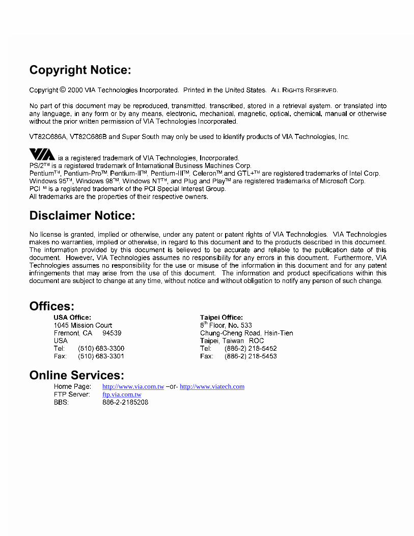
REVISION HISTORY
Document Release Date Revision InitialsRevision 1.6 5/22/00 Initial release based on 82C686A Data Sheet revision 1.6
“CD/CE” info and “CD-CG”silicon revision comments removedAdded Function 0 Rx8 Revision ID of “2x” for 686B
DH
Revision 1.7 6/8/00 Added UDMA100 support to title, feature bullets, and overviewRemoved external APIC support, added IRQ0 input & internal THRM# outputUpdated pin descriptions: MCCS# (U5/U8 select), GPI3, GPI10, GPI11,
GPO6, GPO10, GPO11, GPO21, GPIOC, GPIOD, CHAS, ATEST,THRM, LID
Updated bit descriptions F0 Rx8,41[6],59,74[7],75[6],76[4-3],77[4],85[7-6]Updated bit descriptions F1 Rx41[3-0],42,44[4,2],45[4,1-0],46[5-0],4E-4F,
53-50[28,26-24,20-19,12,4-3],54[5,1,0],70[1-0],74-5,78[1-0],7C-D,C0-7Updated bit descriptions F2/3 Rx43Updated bit descriptions F4 Rx41[1], 4D[3], 55[2], 57[0], D2[2]Updated bit descriptions ACPI I/O Rx5-4[8],Updated bit descriptions SMBus I/O RxUpdated bit descriptions F5 Rx
DH
Revision 1.71 6/9/00 Changed Audio / Game / MIDI ports to dedicated pins (SDD removed)Strap description removed from SPKR pin
DH
VT82C686B
Revision 1.71 June 9, 2000 -ii- Table of Contents
7HFKQRORJLHV ,QF'HOLYHULQJ 9DOXH'HOLYHULQJ 9DOXH
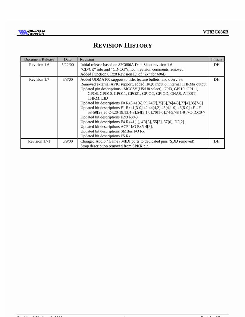
TABLE OF CONTENTS
3& &203/,$17 3&,72,6$ %5,'*( .....................................................................................................................................I
7(03(5$785( 92/7$*( $1' )$163((' 021,725,1*..............................................................................................I
REVISION HISTORY........................................................................................................................................................................I
TABLE OF CONTENTS.................................................................................................................................................................. II
LIST OF FIGURES..........................................................................................................................................................................IV
LIST OF TABLES ...........................................................................................................................................................................IV
OVERVIEW ....................................................................................................................................................................................... 4
PINOUTS............................................................................................................................................................................................ 6
PIN DIAGRAM................................................................................................................................................................................. 6
PIN LISTS........................................................................................................................................................................................ 7
PIN DESCRIPTIONS......................................................................................................................................................................... 9
REGISTERS..................................................................................................................................................................................... 27
REGISTER OVERVIEW ................................................................................................................................................................. 27
REGISTER DESCRIPTIONS............................................................................................................................................................ 39Legacy I/O Ports ................................................................................................................................................................... 39
Keyboard Controller Registers.............................................................................................................................................................. 40DMA Controller I/O Registers .............................................................................................................................................................. 42Interrupt Controller Registers ............................................................................................................................................................... 43Timer / Counter Registers ..................................................................................................................................................................... 43CMOS / RTC Registers......................................................................................................................................................................... 44
Super-I/O Configuration Index / Data Registers ............................................................................................................... 45Super-I/O Configuration Registers ..................................................................................................................................... 45Super-I/O I/O Ports .............................................................................................................................................................. 48
Floppy Disk Controller Registers.......................................................................................................................................................... 48Parallel Port Registers........................................................................................................................................................................... 49Serial Port 1 Registers........................................................................................................................................................................... 50Serial Port 2 Registers........................................................................................................................................................................... 51
SoundBlaster Pro Port Registers......................................................................................................................................... 52FM Registers ......................................................................................................................................................................................... 52Mixer Registers ..................................................................................................................................................................................... 52Sound Processor Registers .................................................................................................................................................................... 52
Game Port Registers ............................................................................................................................................................. 53PCI Configuration Space I/O............................................................................................................................................... 54Function 0 Registers - PCI to ISA Bridge........................................................................................................................... 55
PCI Configuration Space Header .......................................................................................................................................................... 55ISA Bus Control.................................................................................................................................................................................... 55Plug and Play Control ........................................................................................................................................................................... 59Distributed DMA / Serial IRQ Control ................................................................................................................................................. 61Miscellaneous / General Purpose I/O.................................................................................................................................................... 62
Function 1 Registers - Enhanced IDE Controller .............................................................................................................. 68PCI Configuration Space Header .......................................................................................................................................................... 68IDE-Controller-Specific Confiiguration Registers ................................................................................................................................ 70IDE I/O Registers.................................................................................................................................................................................. 74
Function 2 Registers - USB Controller Ports 0-1 ............................................................................................................... 75PCI Configuration Space Header .......................................................................................................................................................... 75USB-Specific Configuration Registers.................................................................................................................................................. 76USB I/O Registers................................................................................................................................................................................. 77
VT82C686B
Revision 1.71 June 9, 2000 -iii- Table of Contents
7HFKQRORJLHV ,QF'HOLYHULQJ 9DOXH'HOLYHULQJ 9DOXH
Function 3 Registers - USB Controller Ports 2-3 ............................................................................................................... 78PCI Configuration Space Header .......................................................................................................................................................... 78USB-Specific Configuration Registers.................................................................................................................................................. 79USB I/O Registers................................................................................................................................................................................. 80
Function 4 Regs - Power Management, SMBus and HWM.............................................................................................. 81PCI Configuration Space Header .......................................................................................................................................................... 81Power Management-Specific PCI Configuration Registers .................................................................................................................. 82Hardware-Monitor-Specific Configuration Registers ........................................................................................................................... 89System Management Bus-Specific Configuration Registers ................................................................................................................. 89Power Management I/O-Space Registers .............................................................................................................................................. 90System Management Bus I/O-Space Registers...................................................................................................................................... 99Hardware Monitor I/O Space Registers .............................................................................................................................................. 102
Function 5 & 6 Registers - AC97 Audio & Modem Codecs ............................................................................................ 106PCI Configuration Space Header – Function 5 Audio ........................................................................................................................ 106PCI Configuration Space Header – Function 6 Modem...................................................................................................................... 107Function 5 & 6 Codec-Specific Configuration Registers .................................................................................................................... 108I/O Base 0 Registers –Audio/Modem Scatter/Gather DMA................................................................................................................ 110I/O Base 1 Registers – Audio FM NMI Status Registers .................................................................................................................... 114I/O Base 2 Registers – MIDI / Game Port........................................................................................................................................... 114I/O Base 3 Registers – Codec Register Shadow.................................................................................................................................. 114Memory Mapped I/O APIC Registers ................................................................................................................................................. 115Indexed I/O APIC 32-Bit Registers..................................................................................................................................................... 115
FUNCTIONAL DESCRIPTIONS ................................................................................................................................................ 117
POWER MANAGEMENT.............................................................................................................................................................. 117Power Management Subsystem Overview .......................................................................................................................................... 117Processor Bus States ........................................................................................................................................................................... 117System Suspend States and Power Plane Control ............................................................................................................................... 118General Purpose I/O Ports................................................................................................................................................................... 118Power Management Events ................................................................................................................................................................. 119System and Processor Resume Events ................................................................................................................................................ 119Legacy Power Management Timers .................................................................................................................................................... 120System Primary and Secondary Events ............................................................................................................................................... 120Peripheral Events ................................................................................................................................................................................ 120
ELECTRICAL SPECIFICATIONS............................................................................................................................................. 121
ABSOLUTE MAXIMUM RATINGS ............................................................................................................................................... 121
DC CHARACTERISTICS.............................................................................................................................................................. 121
PACKAGE MECHANICAL SPECIFICATIONS ...................................................................................................................... 122
VT82C686B
Revision 1.71 June 9, 2000 -iv- Table of Contents
7HFKQRORJLHV ,QF'HOLYHULQJ 9DOXH'HOLYHULQJ 9DOXH
LIST OF FIGURES
FIGURE 1. PC SYSTEM CONFIGURATION USING THE VT82C686B ................................................................................. 5FIGURE 2. VT82C686B BALL DIAGRAM (TOP VIEW)........................................................................................................... 6FIGURE 3. VT82C686B PIN LIST (NUMERICAL ORDER)...................................................................................................... 7FIGURE 4. VT82C686B PIN LIST (ALPHABETICAL ORDER)............................................................................................... 8FIGURE 5. STRAP OPTION CIRCUIT....................................................................................................................................... 60FIGURE 6. POWER MANAGEMENT SUBSYSTEM BLOCK DIAGRAM ......................................................................... 117FIGURE 8. MECHANICAL SPECIFICATIONS – 352 PIN BALL GRID ARRAY PACKAGE......................................... 122
LIST OF TABLES
TABLE 1. PIN DESCRIPTIONS..................................................................................................................................................... 9TABLE 2. SYSTEM I/O MAP ....................................................................................................................................................... 27TABLE 3. REGISTERS.................................................................................................................................................................. 28TABLE 4. KEYBOARD CONTROLLER COMMAND CODES .............................................................................................. 41TABLE 5. CMOS REGISTER SUMMARY................................................................................................................................. 44
VT82C686B
Revision 1.71 June 9, 2000 -1- Features
7HFKQRORJLHV ,QF'HOLYHULQJ 9DOXH'HOLYHULQJ 9DOXH
VT82C686B PSIPCPCI SUPER-I/O INTEGRATED PERIPHERAL CONTROLLER
PC99 COMPLIANT PCI-TO-ISA BRIDGE
WITH INTEGRATED SUPER-I/O (FDC, LPT, COM1/2, AND IR),INTEGRATED HARDWARE SOUNDBLASTER/DIRECT SOUND AC97 AUDIO,
ULTRADMA-33/66/100 MASTER MODE PCI-EIDE CONTROLLER,USB CONTROLLER, KEYBOARD CONTROLLER, RTC,DISTRIBUTED DMA, SERIAL IRQ, PLUG AND PLAY,
ACPI, ENHANCED POWER MANAGEMENT, SMBUS, AND
TEMPERATURE, VOLTAGE, AND FAN-SPEED MONITORING
• Inter-operable with VIA and other Host-to-PCI Bridges
− Combine with VT82C598 for a complete Super-7 (66/75/83/100MHz) PCI / AGP / ISA system (Apollo MVP3)− Combine with VT8501 for a complete Super-7 system with integrated 2D / 3D graphics (Apollo MVP4)− Combine with VT82C693 for a complete 66 / 100 / 133 MHz Socket-370 or Slot-1 system (Apollo Pro133)− Combine with VT8601 for a complete 66 / 100 / 133 MHz Socket-370 or Slot-1 system with integrated 2D / 3D
graphics (Apollo ProMedia)− Inter-operable with Intel or other Host-to-PCI bridges for a complete PC99 compliant PCI / AGP / ISA system
• PCI to ISA Bridge
− Integrated ISA Bus Controller with integrated DMA, timer, and interrupt controller− Integrated Keyboard Controller with PS2 mouse support− Integrated DS12885-style Real Time Clock with extended 256 byte CMOS RAM and Day/Month Alarm for ACPI− Integrated USB Controller with root hub and four function ports− Integrated UltraDMA-33/66/100 master mode EIDE controller with enhanced PCI bus commands− PCI-2.2 compliant with delay transaction and remote power management− Eight double-word line buffer between PCI and ISA bus− One level of PCI to ISA post-write buffer− Supports type F DMA transfers− Distributed DMA support for ISA legacy DMA across the PCI bus− Serial interrupt for docking and non-docking applications− Fast reset and Gate A20 operation− Edge trigger or level sensitive interrupt− Flash EPROM, 4Mb EPROM and combined BIOS support− Supports positive and subtractive decoding
VT82C686B
Revision 1.71 June 9, 2000 -2- Features
7HFKQRORJLHV ,QF'HOLYHULQJ 9DOXH'HOLYHULQJ 9DOXH
• UltraDMA-33 / 66 / 100 Master Mode PCI EIDE Controller
− Dual channel master mode PCI supporting four Enhanced IDE devices− Transfer rate up to 33MB/sec to cover PIO mode 4, multi-word DMA mode 2 drives, and UltraDMA-33 interface− Increased reliability using UltraDMA-66 transfer protocols− Increased performance using UltraDMA-100 mode 5− Thirty-two levels (doublewords) of prefetch and write buffers− Dual DMA engine for concurrent dual channel operation− Bus master programming interface for SFF-8038I rev.1.0 and Windows-95 compliant− Full scatter gather capability− Support ATAPI compliant devices including DVD devices− Support PCI native and ATA compatibility modes− Complete software driver support
• Integrated Super IO Controller
− Supports 2 serial ports, IR port, parallel port, and floppy disk controller functions− Two UARTs for Complete Serial Ports
Programmable character lengths (5,6,7,8)Even, odd, stick or no parity bit generation and detectionProgrammable baud rate generatorHigh speed baud rate (230Kbps, 460Kbps) supportIndependent transmit/receiver FIFOsModem ControlPlug and play with 96 base IO address and 12 IRQ options
− Infrared-IrDA (HPSIR) and ASK (Amplitude Shift Keyed) IR port multiplexed on COM2− Multi-mode parallel port
Standard mode, ECP and EPP supportPlug and play with 192 base IO address, 12 IRQ and 4 DMA options
− Floppy Disk Controller16 bytes of FIFOData rates up to 1MbpsPerpendicular recording driver supportTwo FDDs with drive swap supportPlug and play with 48 base IO address, 12 IRQ and 4 DMA options
• SoundBlaster Pro Hardware and Direct Sound Ready AC97 Digital Audio Controller
− Dual full-duplex Direct Sound channels between system memory and AC97 link− PCI master interface with scatter / gather and bursting capability− 32 byte FIFO of each direct sound channel− Host based sample rate converter and mixer− Standard v1.0 or v2.0 AC97 Codec interface for single or cascaded AC97 Codec’s from multiple vendors− Loopback capability for re-directing mixed audio streams into USB and 1394 speakers− Hardware SoundBlaster Pro for Windows DOS box and real-mode DOS legacy compatibility− Plug and play with 4 IRQ, 4 DMA, and 4 I/O space options for SoundBlaster Pro and MIDI hardware− Hardware assisted FM synthesis for legacy compatibility− Direct two game ports and one MIDI port interface− Complete software driver support for Windows-95/98/2000 and Windows-NT
• Voltage, Temperature, Fan Speed Monitor and Controller
− Five positive voltage (one internal), three temperature (one internal) and two fan-speed monitoring− Programmable control, status, monitor and alarm for flexible desktop management− External thermister or internal bandgap temperature sensing− Automatic clock throttling with integrated temperature sensing− Internal core VCC voltage sensing− Flexible external voltage sensing arrangement (any positive supply and battery)
VT82C686B
Revision 1.71 June 9, 2000 -3- Features
7HFKQRORJLHV ,QF'HOLYHULQJ 9DOXH'HOLYHULQJ 9DOXH
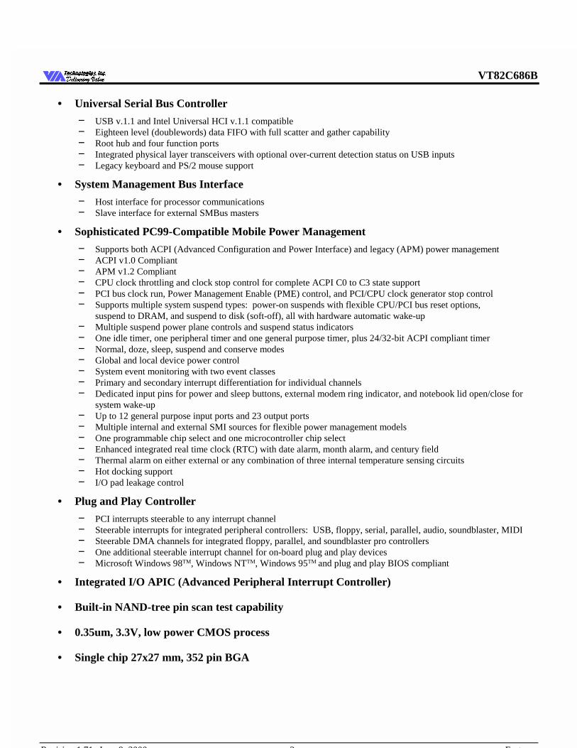
• Universal Serial Bus Controller
− USB v.1.1 and Intel Universal HCI v.1.1 compatible− Eighteen level (doublewords) data FIFO with full scatter and gather capability− Root hub and four function ports− Integrated physical layer transceivers with optional over-current detection status on USB inputs− Legacy keyboard and PS/2 mouse support
• System Management Bus Interface
− Host interface for processor communications− Slave interface for external SMBus masters
• Sophisticated PC99-Compatible Mobile Power Management
− Supports both ACPI (Advanced Configuration and Power Interface) and legacy (APM) power management− ACPI v1.0 Compliant− APM v1.2 Compliant− CPU clock throttling and clock stop control for complete ACPI C0 to C3 state support− PCI bus clock run, Power Management Enable (PME) control, and PCI/CPU clock generator stop control− Supports multiple system suspend types: power-on suspends with flexible CPU/PCI bus reset options,
suspend to DRAM, and suspend to disk (soft-off), all with hardware automatic wake-up− Multiple suspend power plane controls and suspend status indicators− One idle timer, one peripheral timer and one general purpose timer, plus 24/32-bit ACPI compliant timer− Normal, doze, sleep, suspend and conserve modes− Global and local device power control− System event monitoring with two event classes− Primary and secondary interrupt differentiation for individual channels− Dedicated input pins for power and sleep buttons, external modem ring indicator, and notebook lid open/close for
system wake-up− Up to 12 general purpose input ports and 23 output ports− Multiple internal and external SMI sources for flexible power management models− One programmable chip select and one microcontroller chip select− Enhanced integrated real time clock (RTC) with date alarm, month alarm, and century field− Thermal alarm on either external or any combination of three internal temperature sensing circuits− Hot docking support− I/O pad leakage control
• Plug and Play Controller
− PCI interrupts steerable to any interrupt channel− Steerable interrupts for integrated peripheral controllers: USB, floppy, serial, parallel, audio, soundblaster, MIDI− Steerable DMA channels for integrated floppy, parallel, and soundblaster pro controllers− One additional steerable interrupt channel for on-board plug and play devices− Microsoft Windows 98TM, Windows NTTM, Windows 95TM and plug and play BIOS compliant
• Integrated I/O APIC (Advanced Peripheral Interrupt Controller)
• Built-in NAND-tree pin scan test capability
• 0.35um, 3.3V, low power CMOS process
• Single chip 27x27 mm, 352 pin BGA
VT82C686B
Revision 1.71 June 9, 2000 -4- Overview
7HFKQRORJLHV ,QF'HOLYHULQJ 9DOXH'HOLYHULQJ 9DOXH
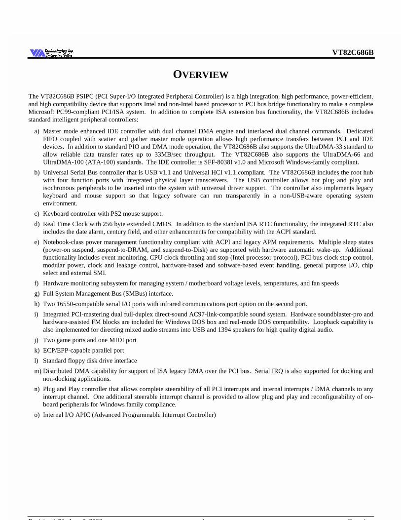
OVERVIEW
The VT82C686B PSIPC (PCI Super-I/O Integrated Peripheral Controller) is a high integration, high performance, power-efficient,and high compatibility device that supports Intel and non-Intel based processor to PCI bus bridge functionality to make a completeMicrosoft PC99-compliant PCI/ISA system. In addition to complete ISA extension bus functionality, the VT82C686B includesstandard intelligent peripheral controllers:
a) Master mode enhanced IDE controller with dual channel DMA engine and interlaced dual channel commands. DedicatedFIFO coupled with scatter and gather master mode operation allows high performance transfers between PCI and IDEdevices. In addition to standard PIO and DMA mode operation, the VT82C686B also supports the UltraDMA-33 standard toallow reliable data transfer rates up to 33MB/sec throughput. The VT82C686B also supports the UltraDMA-66 andUltraDMA-100 (ATA-100) standards. The IDE controller is SFF-8038I v1.0 and Microsoft Windows-family compliant.
b) Universal Serial Bus controller that is USB v1.1 and Universal HCI v1.1 compliant. The VT82C686B includes the root hubwith four function ports with integrated physical layer transceivers. The USB controller allows hot plug and play andisochronous peripherals to be inserted into the system with universal driver support. The controller also implements legacykeyboard and mouse support so that legacy software can run transparently in a non-USB-aware operating systemenvironment.
c) Keyboard controller with PS2 mouse support.
d) Real Time Clock with 256 byte extended CMOS. In addition to the standard ISA RTC functionality, the integrated RTC alsoincludes the date alarm, century field, and other enhancements for compatibility with the ACPI standard.
e) Notebook-class power management functionality compliant with ACPI and legacy APM requirements. Multiple sleep states(power-on suspend, suspend-to-DRAM, and suspend-to-Disk) are supported with hardware automatic wake-up. Additionalfunctionality includes event monitoring, CPU clock throttling and stop (Intel processor protocol), PCI bus clock stop control,modular power, clock and leakage control, hardware-based and software-based event handling, general purpose I/O, chipselect and external SMI.
f) Hardware monitoring subsystem for managing system / motherboard voltage levels, temperatures, and fan speeds
g) Full System Management Bus (SMBus) interface.
h) Two 16550-compatible serial I/O ports with infrared communications port option on the second port.
i) Integrated PCI-mastering dual full-duplex direct-sound AC97-link-compatible sound system. Hardware soundblaster-pro andhardware-assisted FM blocks are included for Windows DOS box and real-mode DOS compatibility. Loopback capability isalso implemented for directing mixed audio streams into USB and 1394 speakers for high quality digital audio.
j) Two game ports and one MIDI port
k) ECP/EPP-capable parallel port
l) Standard floppy disk drive interface
m) Distributed DMA capability for support of ISA legacy DMA over the PCI bus. Serial IRQ is also supported for docking andnon-docking applications.
n) Plug and Play controller that allows complete steerability of all PCI interrupts and internal interrupts / DMA channels to anyinterrupt channel. One additional steerable interrupt channel is provided to allow plug and play and reconfigurability of on-board peripherals for Windows family compliance.
o) Internal I/O APIC (Advanced Programmable Interrupt Controller)
VT82C686B
Revision 1.71 June 9, 2000 -5- Overview
7HFKQRORJLHV ,QF'HOLYHULQJ 9DOXH'HOLYHULQJ 9DOXH
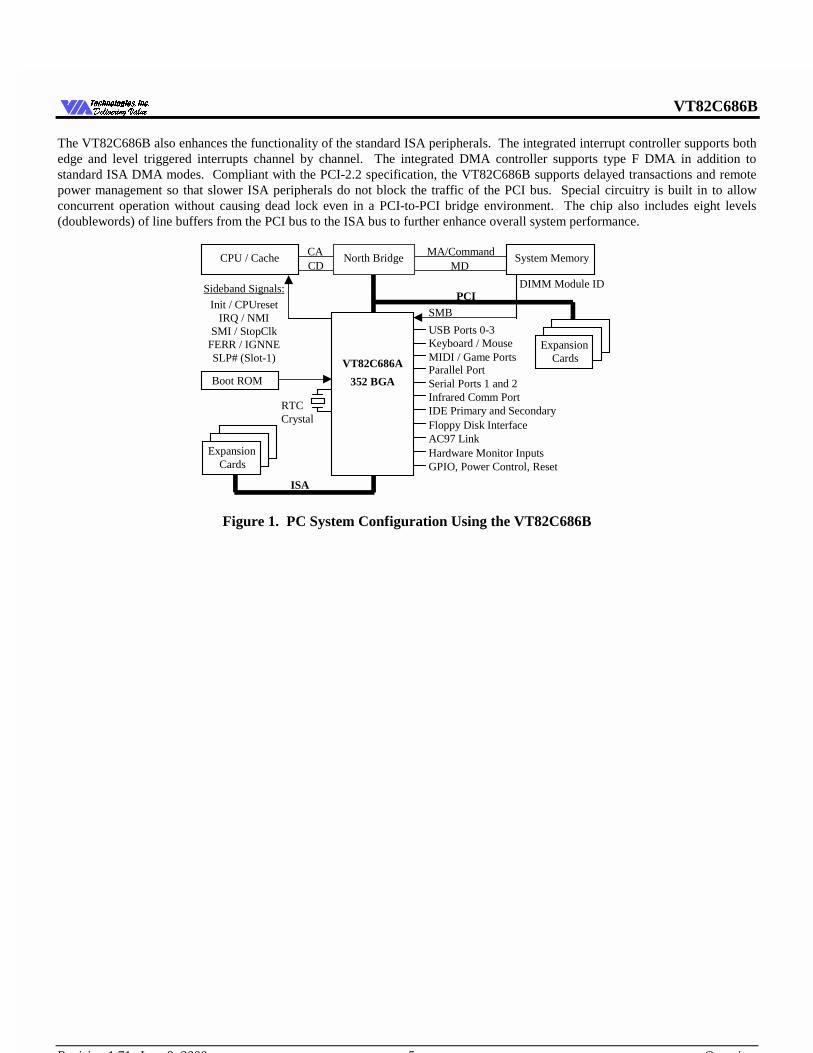
The VT82C686B also enhances the functionality of the standard ISA peripherals. The integrated interrupt controller supports bothedge and level triggered interrupts channel by channel. The integrated DMA controller supports type F DMA in addition tostandard ISA DMA modes. Compliant with the PCI-2.2 specification, the VT82C686B supports delayed transactions and remotepower management so that slower ISA peripherals do not block the traffic of the PCI bus. Special circuitry is built in to allowconcurrent operation without causing dead lock even in a PCI-to-PCI bridge environment. The chip also includes eight levels(doublewords) of line buffers from the PCI bus to the ISA bus to further enhance overall system performance.
CPU / CacheCA
PCI
MDMA/Command
CDNorth Bridge
352 BGA
VT82C686A
System Memory
Sideband Signals:
Init / CPUresetIRQ / NMI
SMI / StopClkFERR / IGNNESLP# (Slot-1)
USB Ports 0-3
Serial Ports 1 and 2
ISA
RTCCrystal
Boot ROM
ExpansionCards
Infrared Comm PortIDE Primary and SecondaryFloppy Disk InterfaceAC97 LinkHardware Monitor Inputs
Keyboard / Mouse
SMB
DIMM Module ID
ExpansionCards GPIO, Power Control, Reset
MIDI / Game PortsParallel Port
Figure 1. PC System Configuration Using the VT82C686B
VT82C686B
Revision 1.71 June 9, 2000 -6- Pinouts
7HFKQRORJLHV ,QF'HOLYHULQJ 9DOXH'HOLYHULQJ 9DOXH
PINOUTS
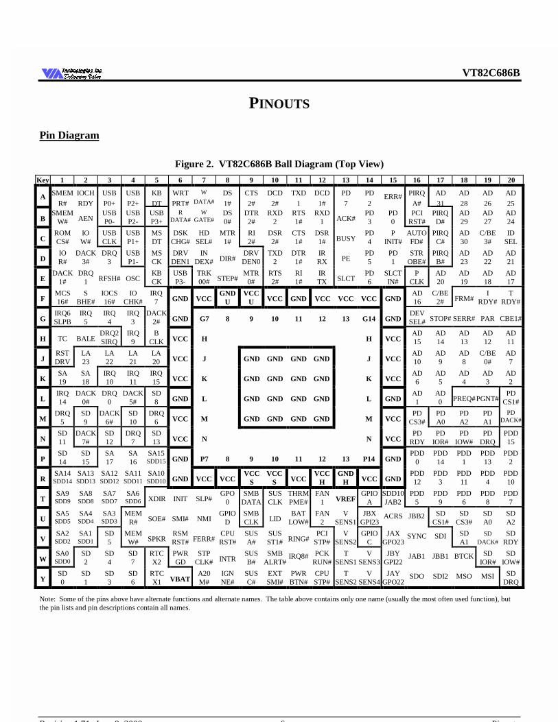
Pin Diagram
Figure 2. VT82C686B Ball Diagram (Top View)
Key 1 2 3 4 5 6 7 8 9 10 11 12 13 14 15 16 17 18 19 20
A SMEM
R#
IOCH
RDY
USB
P0+
USB
P2+
KB
DT
WRT
PRT#
W
DATA#DS
1#
CTS
2#
DCD
2#
TXD
1
DCD
1#
PD
7
PD
2ERR# PIRQ
A#
AD
31
AD
28
AD
26
AD
25
BSMEM
W# AENUSBP0-
USBP2-
USBP3+
RDATA#
WGATE#
DS0#
DTR2#
RXD2
RTS1#
RXD1 ACK#
PD3
PD0
PCIRST#
PIRQD#
AD29
AD27
AD24
CROMCS#
IOW#
USBCLK
USBP1+
MSDT
DSKCHG#
HDSEL#
MTR1#
RI2#
DSR2#
CTS1#
DSR1# BUSY
PD4
PINIT#
AUTOFD#
PIRQC#
AD30
C/BE3#
IDSEL
DIOR#
DACK3#
DRQ3
USBP1-
MSCK
DRVDEN1
INDEX# DIR#
DRVDEN0
TXD2
DTR1#
IRRX PE
PD5
PD1
STROBE#
PIRQB#
AD23
AD22
AD21
EDACK
1#DRQ
1 RFSH# OSCKBCK
USBP3-
TRK00# STEP#
MTR0#
RTS2#
RI1#
IRTX SLCT
PD6
SLCTIN#
PCLK
AD20
AD19
AD18
AD17
FMCS16#
SBHE#
IOCS16#
IOCHK#
IRQ7 GND VCC
GNDU
VCCU VCC GND VCC VCC VCC GND
AD16
C/BE2# FRM#
IRDY#
TRDY#
GIRQ6SLPB
IRQ5
IRQ4
IRQ3
DACK2# GND G7 8 9 10 11 12 13 G14 GND
DEVSEL# STOP# SERR# PAR CBE1#
H TC BALEDRQ2SIRQ
IRQ9
BCLK VCC H H VCC
AD15
AD14
AD13
AD12
AD11
JRSTDRV
LA23
LA22
LA21
LA20 VCC J GND GND GND GND J VCC
AD10
AD9
AD8
C/BE0#
AD7
KSA19
SA18
IRQ10
IRQ11
IRQ15 VCC K GND GND GND GND K VCC
AD6
AD5
AD4
AD3
AD2
LIRQ14
DACK0#
DRQ0
DACK5#
SD8 GND L GND GND GND GND L GND
AD1
AD0 PREQ#PGNT#
PDCS1#
MDRQ
5SD9
DACK6#
SD10
DRQ6 VCC M GND GND GND GND M VCC
PDCS3#
PDA0
PDA2
PDA1
PDDACK#
NSD11
DACK7#
SD12
DRQ7
SD13 VCC N N VCC
PDRDY
PDIOR#
PDIOW#
PDDRQ
PDD15
PSD14
SD15
SA17
SA16
SA15SDD15 GND P7 8 9 10 11 12 13 P14 GND
PDD0
PDD14
PDD1
PDD13
PDD2
RSA14SDD14
SA13SDD13
SA12SDD12
SA11SDD11
SA10SDD10 GND VCC VCC
VCCS
VCCS VCC
VCCH
GNDH VCC GND
PDD12
PDD3
PDD11
PDD4
PDD10
TSA9SDD9
SA8SDD8
SA7SDD7
SA6SDD6 XDIR INIT SLP#
GPO0
SMBDATA
SUSCLK
THRMPME#
FAN1 VREF
GPIOA
SDD10JAB2
PDD5
PDD9
PDD6
PDD8
PDD7
USA5SDD5
SA4SDD4
SA3SDD3
MEMR# SOE# SMI# NMI
GPIOD
SMBCLK LID
BATLOW#
FAN2
VSENS1
JBXGPI23
ACRS JBB2 SDCS1#
SDCS3#
SDA0
SDA2
VSA2SDD2
SA1SDD1
SD5
MEMW# SPKR
RSMRST# FERR#
CPURST#
SUSA#
SUSST1# RING#
PCISTP#
VSENS2
GPIOC
JAXGPO23
SYNC SDI SDA1
SDDACK#
SDRDY
WSA0SDD0
SD2
SD4
SD7
RTCX2
PWRGD
STPCLK# INTR
SUSB#
SMBALRT#
IRQ8# PCKRUN#
TSENS1
VSENS3
JBYGPI22
JAB1 JBB1 BTCK SDIOR#
SDIOW#
YSD0
SD1
SD3
SD6
RTCX1 VBAT
A20M#
IGNNE#
SUSC#
EXTSMI#
PWRBTN#
CPUSTP#
TSENS2
VSENS4
JAYGPO22
SDO SDI2 MSO MSI SDDRQ
Note: Some of the pins above have alternate functions and alternate names. The table above contains only one name (usually the most often used function), butthe pin lists and pin descriptions contain all names.
VT82C686B
Revision 1.71 June 9, 2000 -7- Pinouts
7HFKQRORJLHV ,QF'HOLYHULQJ 9DOXH'HOLYHULQJ 9DOXH
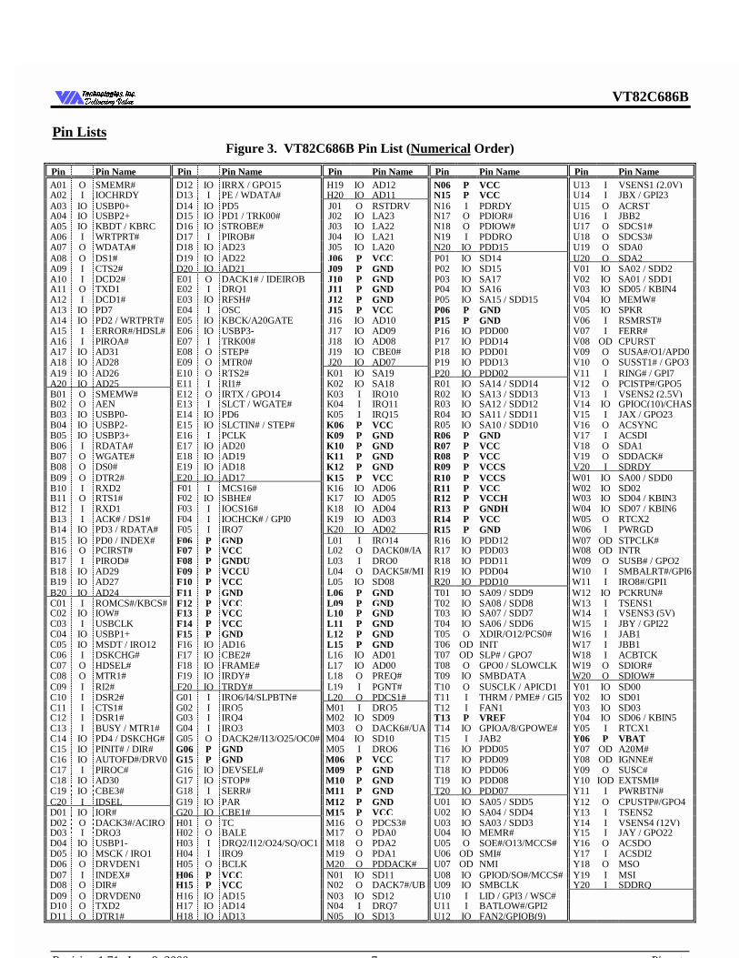
Pin ListsFigure 3. VT82C686B Pin List (Numerical Order)
Pin Pin Name Pin Pin Name Pin Pin Name Pin Pin Name Pin Pin NameA01 O SMEMR# D12 IO IRRX / GPO15 H19 IO AD12 N06 P VCC U13 I VSENS1 (2.0V)A02 I IOCHRDY D13 I PE / WDATA# H20 IO AD11 N15 P VCC U14 I JBX / GPI23A03 IO USBP0+ D14 IO PD5 J01 O RSTDRV N16 I PDRDY U15 O ACRSTA04 IO USBP2+ D15 IO PD1 / TRK00# J02 IO LA23 N17 O PDIOR# U16 I JBB2A05 IO KBDT / KBRC D16 IO STROBE# J03 IO LA22 N18 O PDIOW# U17 O SDCS1#A06 I WRTPRT# D17 I PIRQB# J04 IO LA21 N19 I PDDRQ U18 O SDCS3#A07 O WDATA# D18 IO AD23 J05 IO LA20 N20 IO PDD15 U19 O SDA0A08 O DS1# D19 IO AD22 J06 P VCC P01 IO SD14 U20 O SDA2A09 I CTS2# D20 IO AD21 J09 P GND P02 IO SD15 V01 IO SA02 / SDD2A10 I DCD2# E01 O DACK1# / IDEIRQB J10 P GND P03 IO SA17 V02 IO SA01 / SDD1A11 O TXD1 E02 I DRQ1 J11 P GND P04 IO SA16 V03 IO SD05 / KBIN4A12 I DCD1# E03 IO RFSH# J12 P GND P05 IO SA15 / SDD15 V04 IO MEMW#A13 IO PD7 E04 I OSC J15 P VCC P06 P GND V05 IO SPKRA14 IO PD2 / WRTPRT# E05 IO KBCK/A20GATE J16 IO AD10 P15 P GND V06 I RSMRST#A15 I ERROR#/HDSL# E06 IO USBP3- J17 IO AD09 P16 IO PDD00 V07 I FERR#A16 I PIRQA# E07 I TRK00# J18 IO AD08 P17 IO PDD14 V08 OD CPURSTA17 IO AD31 E08 O STEP# J19 IO CBE0# P18 IO PDD01 V09 O SUSA#/O1/APD0A18 IO AD28 E09 O MTR0# J20 IO AD07 P19 IO PDD13 V10 O SUSST1# / GPO3A19 IO AD26 E10 O RTS2# K01 IO SA19 P20 IO PDD02 V11 I RING# / GPI7A20 IO AD25 E11 I RI1# K02 IO SA18 R01 IO SA14 / SDD14 V12 O PCISTP#/GPO5B01 O SMEMW# E12 O IRTX / GPO14 K03 I IRQ10 R02 IO SA13 / SDD13 V13 I VSENS2 (2.5V)B02 O AEN E13 I SLCT / WGATE# K04 I IRQ11 R03 IO SA12 / SDD12 V14 IO GPIOC(10)/CHASB03 IO USBP0- E14 IO PD6 K05 I IRQ15 R04 IO SA11 / SDD11 V15 I JAX / GPO23B04 IO USBP2- E15 IO SLCTIN# / STEP# K06 P VCC R05 IO SA10 / SDD10 V16 O ACSYNCB05 IO USBP3+ E16 I PCLK K09 P GND R06 P GND V17 I ACSDIB06 I RDATA# E17 IO AD20 K10 P GND R07 P VCC V18 O SDA1B07 O WGATE# E18 IO AD19 K11 P GND R08 P VCC V19 O SDDACK#B08 O DS0# E19 IO AD18 K12 P GND R09 P VCCS V20 I SDRDYB09 O DTR2# E20 IO AD17 K15 P VCC R10 P VCCS W01 IO SA00 / SDD0B10 I RXD2 F01 I MCS16# K16 IO AD06 R11 P VCC W02 IO SD02B11 O RTS1# F02 IO SBHE# K17 IO AD05 R12 P VCCH W03 IO SD04 / KBIN3B12 I RXD1 F03 I IOCS16# K18 IO AD04 R13 P GNDH W04 IO SD07 / KBIN6B13 I ACK# / DS1# F04 I IOCHCK# / GPI0 K19 IO AD03 R14 P VCC W05 O RTCX2B14 IO PD3 / RDATA# F05 I IRQ7 K20 IO AD02 R15 P GND W06 I PWRGDB15 IO PD0 / INDEX# F06 P GND L01 I IRQ14 R16 IO PDD12 W07 OD STPCLK#B16 O PCIRST# F07 P VCC L02 O DACK0#/IA R17 IO PDD03 W08 OD INTRB17 I PIRQD# F08 P GNDU L03 I DRQ0 R18 IO PDD11 W09 O SUSB# / GPO2B18 IO AD29 F09 P VCCU L04 O DACK5#/MI R19 IO PDD04 W10 I SMBALRT#/GPI6B19 IO AD27 F10 P VCC L05 IO SD08 R20 IO PDD10 W11 I IRQ8#/GPI1B20 IO AD24 F11 P GND L06 P GND T01 IO SA09 / SDD9 W12 IO PCKRUN#C01 I ROMCS#/KBCS# F12 P VCC L09 P GND T02 IO SA08 / SDD8 W13 I TSENS1C02 IO IOW# F13 P VCC L10 P GND T03 IO SA07 / SDD7 W14 I VSENS3 (5V)C03 I USBCLK F14 P VCC L11 P GND T04 IO SA06 / SDD6 W15 I JBY / GPI22C04 IO USBP1+ F15 P GND L12 P GND T05 O XDIR/O12/PCS0# W16 I JAB1C05 IO MSDT / IRQ12 F16 IO AD16 L15 P GND T06 OD INIT W17 I JBB1C06 I DSKCHG# F17 IO CBE2# L16 IO AD01 T07 OD SLP# / GPO7 W18 I ACBTCKC07 O HDSEL# F18 IO FRAME# L17 IO AD00 T08 O GPO0 / SLOWCLK W19 O SDIOR#C08 O MTR1# F19 IO IRDY# L18 O PREQ# T09 IO SMBDATA W20 O SDIOW#C09 I RI2# F20 IO TRDY# L19 I PGNT# T10 O SUSCLK / APICD1 Y01 IO SD00C10 I DSR2# G01 I IRQ6/I4/SLPBTN# L20 O PDCS1# T11 I THRM / PME# / GI5 Y02 IO SD01C11 I CTS1# G02 I IRQ5 M01 I DRQ5 T12 I FAN1 Y03 IO SD03C12 I DSR1# G03 I IRQ4 M02 IO SD09 T13 P VREF Y04 IO SD06 / KBIN5C13 I BUSY / MTR1# G04 I IRQ3 M03 O DACK6#/UA T14 IO GPIOA/8/GPOWE# Y05 I RTCX1C14 IO PD4 / DSKCHG# G05 O DACK2#/I13/O25/OC0# M04 IO SD10 T15 I JAB2 Y06 P VBATC15 IO PINIT# / DIR# G06 P GND M05 I DRQ6 T16 IO PDD05 Y07 OD A20M#C16 IO AUTOFD#/DRV0 G15 P GND M06 P VCC T17 IO PDD09 Y08 OD IGNNE#C17 I PIRQC# G16 IO DEVSEL# M09 P GND T18 IO PDD06 Y09 O SUSC#C18 IO AD30 G17 IO STOP# M10 P GND T19 IO PDD08 Y10 IOD EXTSMI#C19 IO CBE3# G18 I SERR# M11 P GND T20 IO PDD07 Y11 I PWRBTN#C20 I IDSEL G19 IO PAR M12 P GND U01 IO SA05 / SDD5 Y12 O CPUSTP#/GPO4D01 IO IOR# G20 IO CBE1# M15 P VCC U02 IO SA04 / SDD4 Y13 I TSENS2D02 O DACK3#/ACIRQ H01 O TC M16 O PDCS3# U03 IO SA03 / SDD3 Y14 I VSENS4 (12V)D03 I DRQ3 H02 O BALE M17 O PDA0 U04 IO MEMR# Y15 I JAY / GPO22D04 IO USBP1- H03 I DRQ2/I12/O24/SQ/OC1 M18 O PDA2 U05 O SOE#/O13/MCCS# Y16 O ACSDOD05 IO MSCK / IRQ1 H04 I IRQ9 M19 O PDA1 U06 OD SMI# Y17 I ACSDI2D06 O DRVDEN1 H05 O BCLK M20 O PDDACK# U07 OD NMI Y18 O MSOD07 I INDEX# H06 P VCC N01 IO SD11 U08 IO GPIOD/SO#/MCCS# Y19 I MSID08 O DIR# H15 P VCC N02 O DACK7#/UB U09 IO SMBCLK Y20 I SDDRQD09 O DRVDEN0 H16 IO AD15 N03 IO SD12 U10 I LID / GPI3 / WSC#D10 O TXD2 H17 IO AD14 N04 I DRQ7 U11 I BATLOW#/GPI2D11 O DTR1# H18 IO AD13 N05 IO SD13 U12 IO FAN2/GPIOB(9)
VT82C686B
Revision 1.71 June 9, 2000 -8- Pinouts
7HFKQRORJLHV ,QF'HOLYHULQJ 9DOXH'HOLYHULQJ 9DOXH
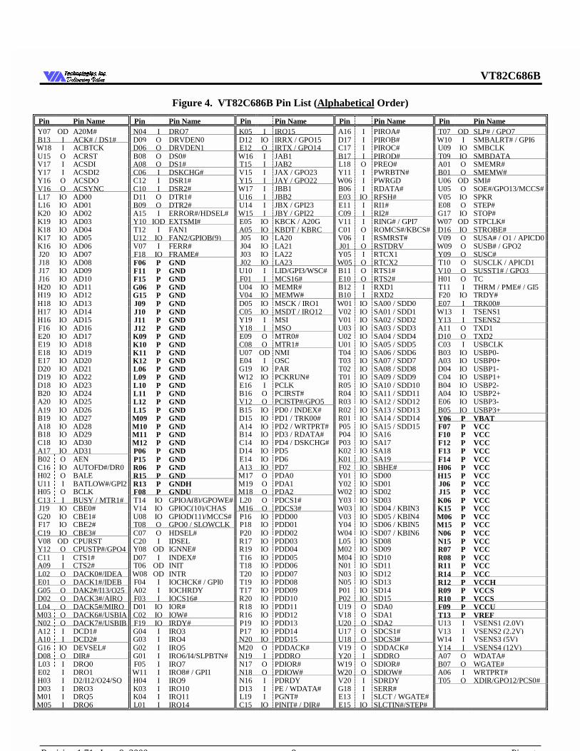
Figure 4. VT82C686B Pin List (Alphabetical Order)
Pin Pin Name Pin Pin Name Pin Pin Name Pin Pin Name Pin Pin NameY07 OD A20M# N04 I DRQ7 K05 I IRQ15 A16 I PIRQA# T07 OD SLP# / GPO7B13 I ACK# / DS1# D09 O DRVDEN0 D12 IO IRRX / GPO15 D17 I PIRQB# W10 I SMBALRT# / GPI6W18 I ACBTCK D06 O DRVDEN1 E12 O IRTX / GPO14 C17 I PIRQC# U09 IO SMBCLKU15 O ACRST B08 O DS0# W16 I JAB1 B17 I PIRQD# T09 IO SMBDATAV17 I ACSDI A08 O DS1# T15 I JAB2 L18 O PREQ# A01 O SMEMR#Y17 I ACSDI2 C06 I DSKCHG# V15 I JAX / GPO23 Y11 I PWRBTN# B01 O SMEMW#Y16 O ACSDO C12 I DSR1# Y15 I JAY / GPO22 W06 I PWRGD U06 OD SMI#V16 O ACSYNC C10 I DSR2# W17 I JBB1 B06 I RDATA# U05 O SOE#/GPO13/MCCS#L17 IO AD00 D11 O DTR1# U16 I JBB2 E03 IO RFSH# V05 IO SPKRL16 IO AD01 B09 O DTR2# U14 I JBX / GPI23 E11 I RI1# E08 O STEP#K20 IO AD02 A15 I ERROR#/HDSEL# W15 I JBY / GPI22 C09 I RI2# G17 IO STOP#K19 IO AD03 Y10 IOD EXTSMI# E05 IO KBCK / A20G V11 I RING# / GPI7 W07 OD STPCLK#K18 IO AD04 T12 I FAN1 A05 IO KBDT / KBRC C01 O ROMCS#/KBCS# D16 IO STROBE#K17 IO AD05 U12 IO FAN2/GPIOB(9) J05 IO LA20 V06 I RSMRST# V09 O SUSA# / O1 / APICD0K16 IO AD06 V07 I FERR# J04 IO LA21 J01 O RSTDRV W09 O SUSB# / GPO2J20 IO AD07 F18 IO FRAME# J03 IO LA22 Y05 I RTCX1 Y09 O SUSC#J18 IO AD08 F06 P GND J02 IO LA23 W05 O RTCX2 T10 O SUSCLK / APICD1J17 IO AD09 F11 P GND U10 I LID/GPI3/WSC# B11 O RTS1# V10 O SUSST1# / GPO3J16 IO AD10 F15 P GND F01 I MCS16# E10 O RTS2# H01 O TCH20 IO AD11 G06 P GND U04 IO MEMR# B12 I RXD1 T11 I THRM / PME# / GI5H19 IO AD12 G15 P GND V04 IO MEMW# B10 I RXD2 F20 IO TRDY#H18 IO AD13 J09 P GND D05 IO MSCK / IRQ1 W01 IO SA00 / SDD0 E07 I TRK00#H17 IO AD14 J10 P GND C05 IO MSDT / IRQ12 V02 IO SA01 / SDD1 W13 I TSENS1H16 IO AD15 J11 P GND Y19 I MSI V01 IO SA02 / SDD2 Y13 I TSENS2F16 IO AD16 J12 P GND Y18 I MSO U03 IO SA03 / SDD3 A11 O TXD1E20 IO AD17 K09 P GND E09 O MTR0# U02 IO SA04 / SDD4 D10 O TXD2E19 IO AD18 K10 P GND C08 O MTR1# U01 IO SA05 / SDD5 C03 I USBCLKE18 IO AD19 K11 P GND U07 OD NMI T04 IO SA06 / SDD6 B03 IO USBP0-E17 IO AD20 K12 P GND E04 I OSC T03 IO SA07 / SDD7 A03 IO USBP0+D20 IO AD21 L06 P GND G19 IO PAR T02 IO SA08 / SDD8 D04 IO USBP1-D19 IO AD22 L09 P GND W12 IO PCKRUN# T01 IO SA09 / SDD9 C04 IO USBP1+D18 IO AD23 L10 P GND E16 I PCLK R05 IO SA10 / SDD10 B04 IO USBP2-B20 IO AD24 L11 P GND B16 O PCIRST# R04 IO SA11 / SDD11 A04 IO USBP2+A20 IO AD25 L12 P GND V12 O PCISTP#/GPO5 R03 IO SA12 / SDD12 E06 IO USBP3-A19 IO AD26 L15 P GND B15 IO PD0 / INDEX# R02 IO SA13 / SDD13 B05 IO USBP3+B19 IO AD27 M09 P GND D15 IO PD1 / TRK00# R01 IO SA14 / SDD14 Y06 P VBATA18 IO AD28 M10 P GND A14 IO PD2 / WRTPRT# P05 IO SA15 / SDD15 F07 P VCCB18 IO AD29 M11 P GND B14 IO PD3 / RDATA# P04 IO SA16 F10 P VCCC18 IO AD30 M12 P GND C14 IO PD4 / DSKCHG# P03 IO SA17 F12 P VCCA17 IO AD31 P06 P GND D14 IO PD5 K02 IO SA18 F13 P VCCB02 O AEN P15 P GND E14 IO PD6 K01 IO SA19 F14 P VCCC16 IO AUTOFD#/DR0 R06 P GND A13 IO PD7 F02 IO SBHE# H06 P VCCH02 O BALE R15 P GND M17 O PDA0 Y01 IO SD00 H15 P VCCU11 I BATLOW#/GPI2 R13 P GNDH M19 O PDA1 Y02 IO SD01 J06 P VCCH05 O BCLK F08 P GNDU M18 O PDA2 W02 IO SD02 J15 P VCCC13 I BUSY / MTR1# T14 IO GPIOA(8)/GPOWE# L20 O PDCS1# Y03 IO SD03 K06 P VCCJ19 IO CBE0# V14 IO GPIOC(10)/CHAS M16 O PDCS3# W03 IO SD04 / KBIN3 K15 P VCCG20 IO CBE1# U08 IO GPIOD(11)/MCCS# P16 IO PDD00 V03 IO SD05 / KBIN4 M06 P VCCF17 IO CBE2# T08 O GPO0 / SLOWCLK P18 IO PDD01 Y04 IO SD06 / KBIN5 M15 P VCCC19 IO CBE3# C07 O HDSEL# P20 IO PDD02 W04 IO SD07 / KBIN6 N06 P VCCV08 OD CPURST C20 I IDSEL R17 IO PDD03 L05 IO SD08 N15 P VCCY12 O CPUSTP#/GPO4 Y08 OD IGNNE# R19 IO PDD04 M02 IO SD09 R07 P VCCC11 I CTS1# D07 I INDEX# T16 IO PDD05 M04 IO SD10 R08 P VCCA09 I CTS2# T06 OD INIT T18 IO PDD06 N01 IO SD11 R11 P VCCL02 O DACK0#/IDEA W08 OD INTR T20 IO PDD07 N03 IO SD12 R14 P VCCE01 O DACK1#/IDEB F04 I IOCHCK# / GPI0 T19 IO PDD08 N05 IO SD13 R12 P VCCHG05 O DAK2#/I13/O25 A02 I IOCHRDY T17 IO PDD09 P01 IO SD14 R09 P VCCSD02 O DACK3#/AIRQ F03 I IOCS16# R20 IO PDD10 P02 IO SD15 R10 P VCCSL04 O DACK5#/MIRQ D01 IO IOR# R18 IO PDD11 U19 O SDA0 F09 P VCCUM03 O DACK6#/USBIA C02 IO IOW# R16 IO PDD12 V18 O SDA1 T13 P VREFN02 O DACK7#/USBIB F19 IO IRDY# P19 IO PDD13 U20 O SDA2 U13 I VSENS1 (2.0V)A12 I DCD1# G04 I IRQ3 P17 IO PDD14 U17 O SDCS1# V13 I VSENS2 (2.2V)A10 I DCD2# G03 I IRQ4 N20 IO PDD15 U18 O SDCS3# W14 I VSENS3 (5V)G16 IO DEVSEL# G02 I IRQ5 M20 O PDDACK# V19 O SDDACK# Y14 I VSENS4 (12V)D08 O DIR# G01 I IRQ6/I4/SLPBTN# N19 I PDDRQ Y20 I SDDRQ A07 O WDATA#L03 I DRQ0 F05 I IRQ7 N17 O PDIOR# W19 O SDIOR# B07 O WGATE#E02 I DRQ1 W11 I IRQ8# / GPI1 N18 O PDIOW# W20 O SDIOW# A06 I WRTPRT#H03 I D2/I12/O24/SQ H04 I IRQ9 N16 I PDRDY V20 I SDRDY T05 O XDIR/GPO12/PCS0#D03 I DRQ3 K03 I IRQ10 D13 I PE / WDATA# G18 I SERR#M01 I DRQ5 K04 I IRQ11 L19 I PGNT# E13 I SLCT / WGATE#M05 I DRQ6 L01 I IRQ14 C15 IO PINIT# / DIR# E15 IO SLCTIN#/STEP#
VT82C686B
Revision 1.71 June 9, 2000 -9- Pinouts
7HFKQRORJLHV ,QF'HOLYHULQJ 9DOXH'HOLYHULQJ 9DOXH
Pin Descriptions
Table 1. Pin Descriptions
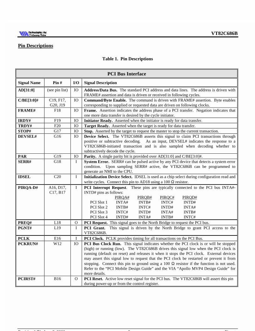
PCI Bus Interface
Signal Name Pin # I/O Signal Description
AD[31:0] (see pin list) IO Address/Data Bus. The standard PCI address and data lines. The address is driven withFRAME# assertion and data is driven or received in following cycles.
C/BE[3:0]# C19, F17,G20, J19
IO Command/Byte Enable. The command is driven with FRAME# assertion. Byte enablescorresponding to supplied or requested data are driven on following clocks.
FRAME# F18 IO Frame. Assertion indicates the address phase of a PCI transfer. Negation indicates thatone more data transfer is desired by the cycle initiator.
IRDY# F19 IO Initiator Ready. Asserted when the initiator is ready for data transfer.TRDY# F20 IO Target Ready. Asserted when the target is ready for data transfer.STOP# G17 IO Stop. Asserted by the target to request the master to stop the current transaction.DEVSEL# G16 IO Device Select. The VT82C686B asserts this signal to claim PCI transactions through
positive or subtractive decoding. As an input, DEVSEL# indicates the response to aVT82C686B-initiated transaction and is also sampled when decoding whether tosubtractively decode the cycle.
PAR G19 IO Parity. A single parity bit is provided over AD[31:0] and C/BE[3:0]#.SERR# G18 I System Error. SERR# can be pulsed active by any PCI device that detects a system error
condition. Upon sampling SERR# active, the VT82C686B can be programmed togenerate an NMI to the CPU.
IDSEL C20 I Initialization Device Select. IDSEL is used as a chip select during configuration read andwrite cycles. Connect this pin to AD18 using a 100 Ω resistor.
PIRQA-D# A16, D17,C17, B17
I PCI Interrupt Request. These pins are typically connected to the PCI bus INTA#-INTD# pins as follows:
PIRQA# PIRQB# PIRQC# PIRQD#PCI Slot 1 INTA# INTB# INTC# INTD#PCI Slot 2 INTB# INTC# INTD# INTA#PCI Slot 3 INTC# INTD# INTA# INTB#PCI Slot 4 INTD# INTA# INTB# INTC#
PREQ# L18 O PCI Request. This signal goes to the North Bridge to request the PCI bus.PGNT# L19 I PCI Grant. This signal is driven by the North Bridge to grant PCI access to the
VT82C686B.PCLK E16 I PCI Clock. PCLK provides timing for all transactions on the PCI Bus.PCKRUN# W12 IO PCI Bus Clock Run. This signal indicates whether the PCI clock is or will be stopped
(high) or running (low). The VT82C686B drives this signal low when the PCI clock isrunning (default on reset) and releases it when it stops the PCI clock. External devicesmay assert this signal low to request that the PCI clock be restarted or prevent it fromstopping. Connect this pin to ground using a 100 Ω resistor if the function is not used.Refer to the “PCI Mobile Design Guide” and the VIA “Apollo MVP4 Design Guide” formore details.
PCIRST# B16 O PCI Reset. Active low reset signal for the PCI bus. The VT82C686B will assert this pinduring power-up or from the control register.
VT82C686B
Revision 1.71 June 9, 2000 -10- Pinouts
7HFKQRORJLHV ,QF'HOLYHULQJ 9DOXH'HOLYHULQJ 9DOXH
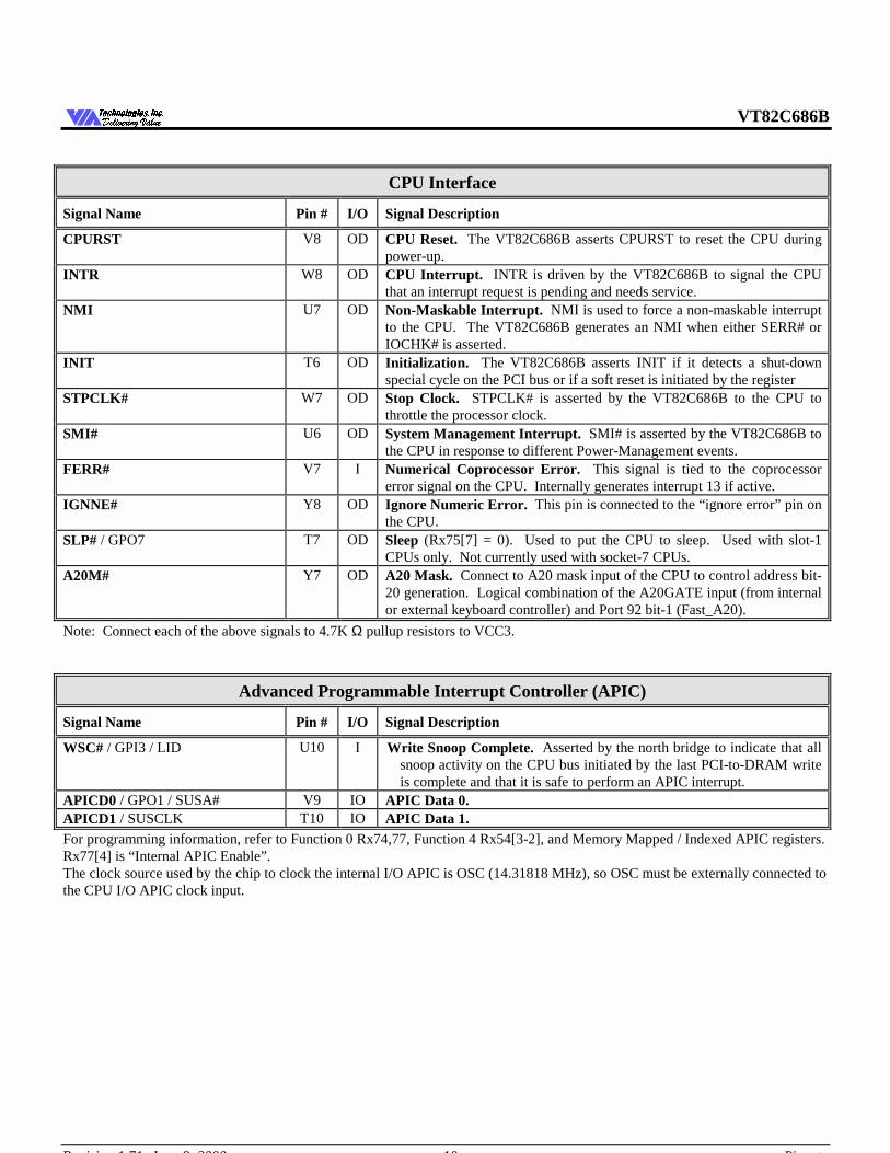
CPU Interface
Signal Name Pin # I/O Signal Description
CPURST V8 OD CPU Reset. The VT82C686B asserts CPURST to reset the CPU duringpower-up.
INTR W8 OD CPU Interrupt. INTR is driven by the VT82C686B to signal the CPUthat an interrupt request is pending and needs service.
NMI U7 OD Non-Maskable Interrupt. NMI is used to force a non-maskable interruptto the CPU. The VT82C686B generates an NMI when either SERR# orIOCHK# is asserted.
INIT T6 OD Initialization. The VT82C686B asserts INIT if it detects a shut-downspecial cycle on the PCI bus or if a soft reset is initiated by the register
STPCLK# W7 OD Stop Clock. STPCLK# is asserted by the VT82C686B to the CPU tothrottle the processor clock.
SMI# U6 OD System Management Interrupt. SMI# is asserted by the VT82C686B tothe CPU in response to different Power-Management events.
FERR# V7 I Numerical Coprocessor Error. This signal is tied to the coprocessorerror signal on the CPU. Internally generates interrupt 13 if active.
IGNNE# Y8 OD Ignore Numeric Error. This pin is connected to the “ignore error” pin onthe CPU.
SLP# / GPO7 T7 OD Sleep (Rx75[7] = 0). Used to put the CPU to sleep. Used with slot-1CPUs only. Not currently used with socket-7 CPUs.
A20M# Y7 OD A20 Mask. Connect to A20 mask input of the CPU to control address bit-20 generation. Logical combination of the A20GATE input (from internalor external keyboard controller) and Port 92 bit-1 (Fast_A20).
Note: Connect each of the above signals to 4.7K Ω pullup resistors to VCC3.
Advanced Programmable Interrupt Controller (APIC)
Signal Name Pin # I/O Signal Description
WSC# / GPI3 / LID U10 I Write Snoop Complete. Asserted by the north bridge to indicate that allsnoop activity on the CPU bus initiated by the last PCI-to-DRAM writeis complete and that it is safe to perform an APIC interrupt.
APICD0 / GPO1 / SUSA# V9 IO APIC Data 0.APICD1 / SUSCLK T10 IO APIC Data 1.For programming information, refer to Function 0 Rx74,77, Function 4 Rx54[3-2], and Memory Mapped / Indexed APIC registers.Rx77[4] is “Internal APIC Enable”.The clock source used by the chip to clock the internal I/O APIC is OSC (14.31818 MHz), so OSC must be externally connected tothe CPU I/O APIC clock input.
VT82C686B
Revision 1.71 June 9, 2000 -11- Pinouts
7HFKQRORJLHV ,QF'HOLYHULQJ 9DOXH'HOLYHULQJ 9DOXH
Universal Serial Bus Interface
Signal Name Pin # I/O Signal Description
USBP0+ A3 IO USB Port 0 Data +USBP0- B3 IO USB Port 0 Data -USBP1+ C4 IO USB Port 1 Data +USBP1- D4 IO USB Port 1 Data -USBP2+ A4 IO USB Port 2 Data +USBP2- B4 IO USB Port 2 Data -USBP3+ B5 IO USB Port 3 Data +USBP3- E6 IO USB Port 3 Data -USBCLK C3 I USB Clock. 48MHz clock input for the USB interfaceUSBOC0# / GPO25 / DACK2# / FDCIRQ G5 I USB Port 0 Over Current Detect. Port 0 is disabled if low.
USBOC0# if Rx76[7] = 1 and Rx76[6] = 0USBOC1# / GPO24 / DRQ2 / FDCDRQ / SERIRQ
H3 I USB Port 1 Over Current Detect. Port 1 is disabled if this inputis low. Direct inputs are provided for overcurrent protection forports 0 and 1 which may be used if the alternate functions of thesetwo pins are not required. If overcurrent protection is desired on allfour ports (or it is desired to use the alternate functions of these twopins), an external buffer may be used to drive the state ofUSBOC[3-0]# onto SD[3-0] during ISA bus refresh cycles (i.e.,while ISA bus RFSH# is low, so that RFSH# may be used as thebuffer enable). USCOC1# if Rx76[7] = 1 and Rx76[6] = 0.
USBOC0# (SD2 & RFSH#) (W2) I USB Port 0 Over Current DetectUSBOC1# (SD1 & RFSH#) (Y2) I USB Port 1 Over Current DetectUSBOC2# (SD0 & RFSH#) (Y1) I USB Port 2 Over Current DetectUSBOC3# (SD3 & RFSH#) (Y3) I USB Port 3 Over Current DetectUSBIRQA / DACK6# M3 O USB Interrupt Request A. Output of internal block.USBIRQB / DACK7# N2 O USB Interrupt Request B. Output of internal block.
System Management Bus (SMB) Interface (I2C Bus)
Signal Name Pin # I/O Signal Description
SMBCLK U9 IO SMB / I2C Clock.SMBDATA T9 IO SMB / I2C Data.SMBALRT# / GPI6 W10 I SMB Alert. (System Management Bus I/O space Rx08[3] = 1)
When the chip is enabled to allow it, assertion generates an IRQ orSMI interrupt or a power management resume event. The same pinis used as General Purpose Input 6 whose value is reflected inRx48[6] of function 4 I/O space
VT82C686B
Revision 1.71 June 9, 2000 -12- Pinouts
7HFKQRORJLHV ,QF'HOLYHULQJ 9DOXH'HOLYHULQJ 9DOXH
UltraDMA-33 / 66 / 100 Enhanced IDE Interface
Signal Name Pin # I/O Signal Description
PDRDY /PDDMARDY /PDSTROBE
N16 I EIDE Mode: Primary I/O Channel Ready. Device ready indicatorUltraDMA Mode: Primary Device DMA Ready. Output flow control. The device
may assert DDMARDY to pause output transfersPrimary Device Strobe. Input data strobe (both edges). Thedevice may stop DSTROBE to pause input data transfers
SDRDY /SDDMARDY /SDSTROBE
V20 I EIDE Mode: Secondary I/O Channel Ready. Device ready indicatorUltraDMA Mode: Secondary Device DMA Ready. Output flow control. The
device may assert DDMARDY to pause output transfersSecondary Device Strobe. Input data strobe (both edges). Thedevice may stop DSTROBE to pause input data transfers
PDIOR# /PHDMARDY /PHSTROBE
N17 O EIDE Mode: Primary Device I/O Read. Device read strobeUltraDMA Mode: Primary Host DMA Ready. Primary channel input flow control.
The host may assert HDMARDY to pause input transfersPrimary Host Strobe. Output data strobe (both edges). Thehost may stop HSTROBE to pause output data transfers
SDIOR# /SHDMARDY /SHSTROBE
W19 O EIDE Mode: Secondary Device I/O Read. Device read strobeUltraDMA Mode: Secondary Host DMA Ready. Input flow control. The host
may assert HDMARDY to pause input transfersHost Strobe B. Output strobe (both edges). The host may stopHSTROBE to pause output data transfers
PDIOW# /PSTOP
N18 O EIDE Mode: Primary Device I/O Write. Device write strobeUltraDMA Mode: Primary Stop. Stop transfer: Asserted by the host prior to
initiation of an UltraDMA burst; negated by the host before datais transferred in an UltraDMA burst. Assertion of STOP by thehost during or after data transfer in UltraDMA mode signals thetermination of the burst.
SDIOW# /SSTOP
W20 O EIDE Mode: Secondary Device I/O Write. Device write strobeUltraDMA Mode: Secondary Stop. Stop transfer: Asserted by the host prior to
initiation of an UltraDMA burst; negated by the host before datais transferred in an UltraDMA burst. Assertion of STOP by thehost during or after data transfer in UltraDMA mode signals thetermination of the burst.
PDDRQ N19 I Primary Device DMA Request. Primary channel DMA requestSDDRQ Y20 I Secondary Device DMA Request. Secondary channel DMA requestPDDACK# M20 O Primary Device DMA Acknowledge. Primary channel DMA acknowledgeSDDACK# V19 O Secondary Device DMA Acknowledge. Secondary channel DMA acknowledgeIRQ14 L1 I Primary Channel Interrupt.IRQ15 K5 I Secondary Channel Interrupt.
VT82C686B
Revision 1.71 June 9, 2000 -13- Pinouts
7HFKQRORJLHV ,QF'HOLYHULQJ 9DOXH'HOLYHULQJ 9DOXH
UltraDMA-33 / 66 / 100 Enhanced IDE Interface (continued)
Signal Name Pin # I/O Signal Description
PDCS1# L20 O Primary Master Chip Select. This signal corresponds to CS1FX# onthe primary IDE connector.
PDCS3# M16 O Primary Slave Chip Select. This signal corresponds to CS3FX# on theprimary IDE connector.
SDCS1# U17 O Secondary Master Chip Select. This signal corresponds to CS17X# onthe secondary IDE connector.
SDCS3# U18 O Secondary Slave Chip Select. This signal corresponds to CS37X# onthe secondary IDE connector.
PDA[2-0] M18, M19, M17 O Primary Disk Address. PDA[2:0] are used to indicate which byte ineither the ATA command block or control block is being accessed.
SDA[2-0] U20, V18, U19 O Secondary Disk Address. SDA[2:0] are used to indicate which byte ineither the ATA command block or control block is being accessed.
PDD[15-0] N20, P17, P19, R16,R18, R20, T17, T19,T20, T18, T16, R19,R17, P20, P18, P16
IO Primary Disk Data
SDD[15-0] / SA[15-0] P5, R1-R5, T1-T4,U1-U3, V1, V2, W1
IO Secondary Disk Data muxed with ISA Bus Address.
IDEIRQA / DACK0# L2 O IDE Interrupt Request A. Output of internal block.IDEIRQB / DACK1# E1 O IDE Interrupt Request B. Output of internal block.
VT82C686B
Revision 1.71 June 9, 2000 -14- Pinouts
7HFKQRORJLHV ,QF'HOLYHULQJ 9DOXH'HOLYHULQJ 9DOXH
MIDI Interface
Signal Name Pin # I/O Signal Description
MSI Y19 I MIDI Serial InMSO Y18 O MIDI Serial Out
AC97 Audio / Modem Interface
Signal Name Pin # I/O Signal Description
ACRST U15 O AC97 ResetACSDOUT Y16 O AC97 Serial Data OutACSYNC V16 O AC97 SyncACSDIN2 Y17 I AC97 Serial Data In 2ACSDIN V17 I AC97 Serial Data InACBTCK W18 I AC97 Bit ClockAC97IRQ / DACK3# D2 O AC97 Interrupt Request. Output of internal block.MC97IRQ / DACK5# / SERIRQ / GPO19
L4 O MC97 Interrupt Request. Output of internal block. Rx77[7] = 1, Rx77[3] = 1,Rx74[6] = 0.
Game Port Interface
Signal Name Pin # I/O Signal Description
JAB1 W16 I Joystick A Button 1JAB2 T15 I Joystick A Button 2JBB1 W17 I Joystick B Button 1JBB2 U16 I Joystick B Button 2JAX / GPO23 V15 I Joystick A X-axisJAY / GPO22 Y15 I Joystick A Y-axisJBX / GPI23 U14 I Joystick B X-axisJBY / GPI22 W15 I Joystick B Y-axisSee Function 0 Rx77[6]
VT82C686B
Revision 1.71 June 9, 2000 -15- Pinouts
7HFKQRORJLHV ,QF'HOLYHULQJ 9DOXH'HOLYHULQJ 9DOXH
Floppy Disk Interface
Signal Name Pin # I/O Signal Description
DRVDEN0 D9 O Drive Density Select 0.DRVDEN1 D6 O Drive Density Select 1.MTR0# E9 O Motor Control 0. Select motor on drive 0.MTR1# C8 O Motor Control 1. Select motor on drive 1DS0# B8 O Drive Select 0. Select drive 0.DS1# A8 O Drive Select 1. Select drive 1DIR# D8 O Direction. Direction of head movement (0 = inward motion, 1 = outward motion)STEP# E8 O Step. Low pulse for each track-to-track movement of the head.INDEX# D7 I Index. Sense to detect that the head is positioned over the beginning of a trackHDSEL# C7 O Head Select. Selects the side for R/W operations (0 = side 1, 1 = side 0)TRK00# E7 I Track 0. Sense to detect that the head is positioned over track 0.RDATA# B6 I Read Data. Raw serial bit stream from the drive for read operatrions.WDATA# A7 O Write Data. Encoded data to the drive for write operations.WGATE# B7 O Write Gate. Signal to the drive to enable current flow in the write head.DSKCHG# C6 I Disk Change. Sense that the drive door is open or the diskette has been changed
since the last drive selection.WRTPRT# A6 I Write Protect. Sense for detection that the diskette is write protected (causes write
commands to be ignored)FDCIRQ / DACK2# / USBOC0# / GPO25
G5 I FDC Interrupt Request. Rx75[2] = 0.
FDCDRQ / DRQ2 / USBOC1# / GPO24 / SERIRQ
H3 I FDC DMA Request. Rx75[3] = 1.
VT82C686B
Revision 1.71 June 9, 2000 -16- Pinouts
7HFKQRORJLHV ,QF'HOLYHULQJ 9DOXH'HOLYHULQJ 9DOXH
Parallel Port Interface
Signal Name Pin # I/O Signal Description
PINIT# / DIR# C15 IO / O Initialize. Initialize printer. Output in standard mode, I/O in ECP/EPP mode.STROBE# / nc D16 IO / - Strobe. Output used to strobe data into the printer. I/O in ECP/EPP mode.AUTOFD# / DRVEN0 C16 IO / O Auto Feed. Output used to cause the printer to automatically feed one line after
each line is printed. I/O pin in ECP/EPP mode.SLCTIN# / STEP# E15 IO / O Select In. Output used to select the printer. I/O pin in ECP/EPP mode.SLCT / WGATE# E13 I / O Select. Status output from the printer. High indicates that it is powered on.ACK# / DS1# B13 I / O Acknowledge. Status output from the printer. Low indicates that it has received
the data and is ready to accept new dataERROR# / HDSEL# A15 I / O Error. Status output from the printer. Low indicates an error condition in the
printer.BUSY / MTR1# C13 I / O Busy. Status output from the printer. High indicates not ready to accept data.PE / WDATA# D13 I / O Paper End. Status output from the printer. High indicates that it is out of paper.PD7 / nc,PD6 / nc,PD5 / nc,PD4 / DSKCHG#,PD3 / RDATA#,PD2 / WRTPRT#,PD1 / TRK00#,PD0 / INDEX#
A13,E14,D14,C14,B14,A14,D15,B15
IO / -IO / -IO / -IO / IIO / IIO / IIO / IIO / I
Parallel Port Data.
As shown by the alternate functions above, in mobile applications the parallel port pins can optionally be selected to function as afloppy disk interface for attachment of an external floppy drive using the parallel port connector (see Super I/O ConfigurationIndex F6[5]).

VT82C686B
Revision 1.71 June 9, 2000 -17- Pinouts
7HFKQRORJLHV ,QF'HOLYHULQJ 9DOXH'HOLYHULQJ 9DOXH
Serial Ports and Infrared InterfaceSignal Name Pin # I/O Signal Description
TXD1 A11 O Transmit Data 1. Serial port 1 transmit data out.TXD2 D10 O Transmit Data 2. Serial port 2 transmit data out.IRTX / GPO14 E12 O Infrared Transmit. IR transmit data out (Rx76[5] = 0) from serial port 2.
General Purpose Output 14 if Rx76[5] = 1RXD1 B12 I Receive Data 1. Serial port 1 receive data in.RXD2 B10 I Receive Data 2. Serial port 2 receive data in.IRRX / GPO15 D12 IO Infrared Receive. IR receive data in (Rx76[5] = 0) to serial port 2. General
Purpose Output 15 if Rx76[5] = 1
RTS1# B11 O Request To Send 1. Indicator that serial output port 1 is ready to transmit data.Typically used as hardware handshake with CTS1# for low level flow control.Designed for direct input to external RS-232C driver.
RTS2## E10 O Request To Send 2. Indicator that serial output port 2 is ready to transmit data.Typically used as hardware handshake with CTS2# for low level flow control.Designed for direct input to external RS-232C driver.
CTS1# C11 I Clear To Send 1. Indicator to serial port 1 that external communications device isready to receive data. Typically used as hardware handshake with RTS1# for lowlevel flow control. Designed for input from external RS-232C receiver.
CTS2# A9 I Clear To Send 2. Indicator to serial port 2 that external communications device isready to receive data. Typically used as hardware handshake with RTS2# for lowlevel flow control. Designed for input from external RS-232C receiver.
DTR1# D11 O Data Terminal Ready 1. Serial port 1 indicator that port is powered, initialized,and ready. Typically used as hardware handshake with DSR1# for overallreadiness to communicate. Designed for direct input to external RS-232C driver.
DTR2# B9 O Data Terminal Ready 2. Serial port 2 indicator that port is powered, initialized,and ready. Typically used as hardware handshake with DSR2# for overallreadiness to communicate. Designed for direct input to external RS-232C driver.
DSR1# C12 I Data Set Ready 1. Indicator to serial port 1 that external serial communicationsdevice is powered, initialized, and ready. Typically used as hardware handshakewith DTR1# for overall readiness to communicate. Designed for direct input fromexternal RS-232C receiver.
DSR2# C10 I Data Set Ready 2. Indicator to serial port 2 that external serial communicationsdevice is powered, initialized, and ready. Typically used as hardware handshakewith DTR2# for overall readiness to communicate. Designed for direct input fromexternal RS-232C receiver.
DCD1# A12 I Data Carrier Detect 1. Indicator to serial port 1 that external modem is detectinga carrier signal (i.e., a communications channel is currently open). In directconnect environments, this input will typically be driven by DTR1# as part of theDTR/DSR handshake. Designed for direct input from external RS-232C receiver.
DCD2# A10 I Data Carrier Detect 2. Indicator to serial port 2 that external modem is detectinga carrier signal (i.e., a communications channel is currently open). In directconnect environments, this input will typically be driven by DTR2# as part of theDTR/DSR handshake. Designed for direct input from external RS-232C receiver.
RI1# E11 I Ring Indicator 1. Indicator to serial port 1 that external modem is detecting aring condition. Used by software to initiate operations to answer and open thecommunications channel. Designed for direct input from external RS-232Creceiver (whose input is typically not connected in direct connect environments).
RI2# C9 I Ring Indicator 2. Indicator to serial port 2 that external modem is detecting aring condition. Used by software to initiate operations to answer and open thecommunications channel. Designed for direct input from external RS-232Creceiver (whose input is typically not connected in direct connect environments).
VT82C686B
Revision 1.71 June 9, 2000 -18- Pinouts
7HFKQRORJLHV ,QF'HOLYHULQJ 9DOXH'HOLYHULQJ 9DOXH
ISA Bus Interface
Signal Name Pin # I/O Signal Description
SA[19:16],SA[15-0] /SDD[15-0]
K1, K2, P3, P4,P5, R1, R2, R3,R4, R5, T1, T2,T3, T4, U1, U2,
U3, V1, V2,W1
IOIO
System Address Bus. SA[19-16] are connected to ISA bus SA[19-16] directly.SA[19-17] are also connected to LA[19-17] of the ISA bus. If the audio interface isdisabled (SPKR pin strapped low), SA[15-0] are connected directly to ISA addressbus pins SA[15-0] (the audio interface pins are used for the IDE secondary data bus).If the audio interface is enabled (SPKR pin strapped high), SA[15-0] are multiplexedwith the IDE Secondary Data Bus. In this case, SA[15-0] may be connected to bothSDD[15-0] and ISA bus SA[15-0]. However, if ISA address bus loading is aconcern, 74F245 transceivers may be used to externally drive ISA address bus pinsSA[15-0]. In this case, these pins would connect directly to the IDE secondary databus and to the transceiver “A” pins and the ISA address bus would connect to thetransceiver “B” pins. SOE# would be used to control the transceiver output enablesand the ISA bus MASTER# signal would drive the transceiver direction controls.
LA[23:20] J2, J3, J4, J5 IO System “Latched” Address Bus: The LA[23:20] address lines are bi-directional.These address lines allow accesses to physical memory on the ISA bus up to16Mbytes. LA[19-17] on the ISA bus are connected to SA[19-17] (see notes above).
SD[15:0] P2, P1, N5, N3,N1, M4, M2,L5, W4, Y4,V3, W3, Y3,W2, Y2, Y1
IO System Data. SD[15:0] provide the data path for devices residing on the ISA bus.X-Bus data signals XD[7:0] may be derived if needed from SD[7:0] using anexternal 74F245-type transceiver (see the XDIR pin description for transceiverconnection details).SD7:4 are strap options for keyboard inputs 6:3 (see Function 0 Rx5A)
SBHE# F2 IO System Byte High Enable. SBHE# indicates, when asserted, that a byte is beingtransferred on the upper byte (SD[15:8]) of the data bus. SBHE# is negated duringrefresh cycles.
IOR# D1 IO I/O Read. IOR# is the command to an ISA I/O slave device that the slave may drivedata on to the ISA data bus.
IOW# C2 IO I/O Write. IOW# is the command to an ISA I/O slave device that the slave maylatch data from the ISA data bus.
MEMR# U4 IO Memory Read. MEMR# is the command to a memory slave that it may drive dataonto the ISA data bus.
MEMW# V4 IO Memory Write. MEMW# is the command to a memory slave that it may latch datafrom the ISA data bus.
SMEMR# A1 O Standard Memory Read. SMEMR# is the command to a memory slave, under1MB, which indicates that it may drive data onto the ISA data bus
SMEMW# B1 O Standard Memory Write. SMEMW# is the command to a memory slave, under1MB, which indicates that it may latch data from the ISA data bus.
BALE H2 O Bus Address Latch Enable. BALE is an active high signal asserted by theVT82C686B to indicate that the address (SA[19:0], LA[23:17] and the SBHE#signal) is valid
IOCS16# F3 I 16-Bit I/O Chip Select. This signal is driven by I/O devices on the ISA Bus toindicate that they support 16-bit I/O bus cycles.
MCS16# F1 I Memory Chip Select 16. ISA slaves that are 16-bit memory devices drive this linelow to indicate they support 16-bit memory bus cycles.
IOCHCK# /GPI0
F4 I I/O Channel Check (Rx74[0] = 1). When this signal is asserted, it indicates that aparity or an uncorrectable error has occurred for an I/O or memory device on theISA Bus. The same pin may optionally be used as General Purpose Input 0.
IOCHRDY A2 I I/O Channel Ready (Rx74[0] = 1). This signal is normally high. Devices on theISA Bus assert IOCHRDY low to indicate that additional time (wait states) isrequired to complete the cycle.
AEN B2 O Address Enable. AEN is asserted during DMA cycles to prevent I/O slaves frommisinterpreting DMA cycles as valid I/O cycles.
VT82C686B
Revision 1.71 June 9, 2000 -19- Pinouts
7HFKQRORJLHV ,QF'HOLYHULQJ 9DOXH'HOLYHULQJ 9DOXH
ISA Bus Interface (continued)
Signal Name Pin # I/O Signal Description
RFSH# E3 IO Refresh. Indicates when a refresh cycle is in progress. Also driven by 16-bit ISA Bus masters to indicate a refresh cycle.
IRQ0 / GPI10 / GPO10 / GPIOC / CHAS / ATEST
V14 I Interrupt Request 0. (Rx77[3] = 1)
IRQ1 / MSCK D5 I Interrupt Request 1. (Rx5A[1] = 0) (used for external KBC interrupt)IRQ3 G4 I Interrupt Request 3. (typically used for COM2 serial port interrupt)IRQ4 G3 I Interrupt Request 4. (typically used for COM1 serial port interrupt)IRQ5 G2 I Interrupt Request 5.IRQ6 / GPI4 / SLPBTN# G1 I Interrupt Request 6. (typically used for FDC floppy ctrlr interrupt)IRQ7 F5 I Interrupt Request 7. (typically used for LPT parallel port interrupt)IRQ8# / GPI1 W11 I Interrupt Request 8 from ext RTC if int RTC disabled (Rx5A[2] = 0)IRQ9 H4 I Interrupt Request 9.IRQ10 K3 I Interrupt Request 10.IRQ11 K4 I Interrupt Request 11.IRQ12 / MSDT C5 I Interrupt Request 12. (Rx5A[1] = 0)IRQ14 L1 I Interrupt Request 14. (typically used for IDE primary chan interrupt)IRQ15 K5 I Interrupt Request 15. (typically used for IDE secondary ch interrupt)DRQ7 / GPI21,DRQ6 / GPI20,DRQ5 / GPI19,DRQ3 / GPI18,DRQ2 / FDCDRQ / SERIRQ / GPO24 / USBOC1#DRQ1 / GPI17,DRQ0 / GPI16
N4,M5,M1,D3,H3,
E2,L3
IIIII
II
DMA Request. Used to request DMA services from the internal DMAcontroller.
DRQ2: Rx68[3] = 0 & Rx75[3] = 1 & Rx75[1] = 0See also Function 0 Rx77[7]
DACK7# / USBIRQB / GPO21 / THRM#,DACK6# / USBIRQA / GPO20,DACK5# / MC97IRQ / GPO19 / SERIRQ,DACK3# / AC97IRQ / GPO18,DACK2# / USBOC0# / GPO25 / FDCIRQDACK1# / IDEIRQB / GPO17,DACK0# / IDEIRQA / GPO16
N2,
M3,L4,
D2,G5,
E1,L2
O
OO
OO
OO
Acknowledge. Used by the internal DMA controller to indicate that arequest for DMA service has been granted.
DACK5#: Rx77[7] = 0
DACK2#: Rx68[3] = 0 & Rx75[3] = 1 & Rx75[2] = 0See also Function 0 Rx77[7], Rx77[3], and Rx58
TC H1 O Terminal Count. Terminal count indicator asserted to DMA slaves.SPKR V5 O Speaker Drive. Output of internal timer/counter 2.SOE# (default pin function)/ GPO13/ MCCS#
U5 O ISA Address (SA) Output Enable. Asserted low when ISA address (SA) isvalid (deasserted when SDD is valid) when SA and SDD are multiplexed onSA pins 15-0 (i.e., when SPKR is strapped low to enable the audio interfacepins). SOE# is tied directly to the output enable of 74F245 transceivers thatbuffer IDE Secondary Bus data and ISA-address (see SA pins for moreinformation).
VT82C686B
Revision 1.71 June 9, 2000 -20- Pinouts
7HFKQRORJLHV ,QF'HOLYHULQJ 9DOXH'HOLYHULQJ 9DOXH
XD Interface
Signal Name Pin # I/O Signal Description
XDIR / PCS0# / GPO12 T5 O X-Bus Data Direction. (Rx76[1]=0) Asserted low for all I/O read cycles and formemory read cycles to the programmed BIOS address space. XDIR is tieddirectly to the direction control of a 74F245 transceiver that buffers the X-Busdata and ISA-Bus data. The transceiver output enable may be grounded. SD0-7connect to the “A” side of the transceiver and XD0-7 connect to the “B” side.XDIR high indicates that SD0-7 drives XD0-7.
Serial IRQ
Signal Name Pin # I/O Signal Description
SERIRQ / DRQ2 / GPO24 / FDCDRQ / USBOC1#
H3 I Serial IRQ (Rx68[3] = 1, Rx74[6] = 0 and Rx75[3] = 1)
SERIRQ / DACK5# / GPO19 / MC97IRQ
L4 I Serial IRQ (Rx68[3] = 1 and Rx74[6] = 1)
VT82C686B
Revision 1.71 June 9, 2000 -21- Pinouts
7HFKQRORJLHV ,QF'HOLYHULQJ 9DOXH'HOLYHULQJ 9DOXH
Internal Keyboard Controller
Signal Name Pin # I/O Signal Description
MSCK / IRQ1 D5 IO / I MultiFunction Pin (Internal mouse controller enabled by Rx5A[1])Rx5A[1]=1 Mouse Clock. From internal mouse controller.Rx5A[1]=0 Interrupt Request 1. Interrupt input 1.
MSDT / IRQ12 C5 IO / I MultiFunction Pin (Internal mouse controller enabled by Rx5A[1])Rx5A[1]=1 Mouse Data. From internal mouse controller.Rx5A[1]=0 Interrupt Request 12. Interrupt input 12.
KBCK / A20GATE E5 IO / I MultiFunction Pin (Internal keyboard controller enabled by Rx5A[0])Rx5A[0]=1 Keyboard Clock. From internal keyboard controllerRx5A[0]=0 Gate A20. Input from external keyboard controller.
KBDT / KBRC A5 IO / I MultiFunction Pin (Internal keyboard controller enabled by Rx5A[0])Rx5A[0]=1 Keyboard Data. From internal keyboard controller.Rx5A[0]=0 Keyboard Reset. From external keyboard controller (KBC)for CPURST# generation
KBCS# / ROMCS# / strap C1 O / O / I Keyboard Chip Select (Rx5A[0]=0). To external keyboard controller chip.Power-Up Configuration Strap (Sampled At Reset):
4.7K to GND = Socket-7, 4.7K to VCC3 = Socket-370 / Slot-1KBIN[6-3] / SD[7-4] W4,
Y4,V3,W3
I / IO Keyboard Inputs 6-3. Sampled at reset on SD[7-4] and latched intoRx5A[7-4].
Chip Selects
Signal Name Pin # I/O Signal Description
ROMCS# / KBCS# / strap C1 O ROM Chip Select (Rx5A[0]=1). Chip Select to the BIOS ROM.Power-Up Configuration Strap (Sampled At Reset):
4.7K to GND = Socket-7, 4.7K to VCC3 = Socket-370 / Slot-1PCS0# / GPO12 / XDIR T5 O Programmable Chip Select 0 (Rx76[1] = 1 and Rx8B[0] = 1). Asserted
during I/O cycles to programmable read or write ISA I/O port ranges.Addressed devices drive data to the SD pins (XDIR is disabled and the X-Bus is not implemented). See also Rx59[3] and Rx77[2].
MCCS# / GPO13 / SOE# U5 O Microcontroller Chip Select (Rx76[3] = 1, Rx76[4] = 0, Rx77[0] = 1).Asserted during read or write accesses to I/O ports 62h or 66h.
MCCS# / GPI11 / GPO11 / GPIOD
U8 O Microcontroller Chip Select (Alternate Pin) (Rx76[4] = 0 selects MCCS#on pin U8, Rx76[4] = 1 selects MCCS# on pin U5). Rx76[3] = 1 enablesMCCS# output on the selected pin.
VT82C686B
Revision 1.71 June 9, 2000 -22- Pinouts
7HFKQRORJLHV ,QF'HOLYHULQJ 9DOXH'HOLYHULQJ 9DOXH
General Purpose Inputs
Signal Name Pin # I/O Signal Description
GPI0 / IOCHCK# F4 I General Purpose Input 0 (Rx74[0] = 0)GPI1 / IRQ8# W11 I General Purpose Input 1 (Rx5A[2] = 1)GPI2 / BATLOW# U11 I General Purpose Input 2GPI3 / LID / WSC# U10 I General Purpose Input 3 (see Rx74[7] and Rx77[3])GPI4 / IRQ6 / SLPBTN# G1 I General Purpose Input 4GPI5 / THRM / PME# T11 I General Purpose Input 5 (Read pin state at PMU IO Rx48[5])GPI6 / SMBALRT# W10 I General Purpose Input 6GPI7 / RING# V11 I General Purpose Input 7GPI8 / GPO8 / GPIOA / GPOWE# T14 I General Purpose Input 8 (Rx74[2] = 0)GPI9 / GPO9 / GPIOB / FAN2 / DTEST U12 I General Purpose Input 9 (Rx74[3] = 0)GPI10 / GPO10 / GPIOC / CHAS / IRQ0 / ATEST
V14 I General Purpose Input 10 (Rx74[4] = 0)
GPI11 / GPO11 / GPIOD / MCCS# U8 I General Purpose Input 11 (Rx74[5] = 0)GPI16 / DRQ0 L3 I General Purpose Input 16 (Rx77[7] = 1). Read at PMU IO 44[2]GPI17 / DRQ1 E2 I General Purpose Input 17 (Rx77[7] = 1). Read at PMU IO 44[3]GPI18 / DRQ3 D3 I General Purpose Input 18 (Rx77[7] = 1)GPI19 / DRQ5 M1 I General Purpose Input 19 (Rx77[7] = 1)GPI20 / DRQ6 M5 I General Purpose Input 20 (Rx77[7] = 1)GPI21 / DRQ7 N4 I General Purpose Input 21 (Rx77[7] = 1)GPI22 / JBY W15 I General Purpose Input 22 (Rx77[6] = 1, game disa)GPI23 / JBX U14 I General Purpose Input 23 (Rx77[6] = 1, game disa)GPI[23-16] (SD[7-0] & RFSH#) n/a I General Purpose Inputs 16-23 (enabled on SD by RFSH# active)
GPI if Rx77[7] = 0 , SD if Rx77[7] = 1
See also Function 0 Rx77[7-6]

VT82C686B
Revision 1.71 June 9, 2000 -23- Pinouts
7HFKQRORJLHV ,QF'HOLYHULQJ 9DOXH'HOLYHULQJ 9DOXH
General Purpose Outputs
Signal Name Pin # I/O Signal Description
GPO0 (H) / SLOWCLK T8 O General Purpose Output 0 (Function 4 Rx54[1-0] = 00). Output valuedetermined by PMU I/O Rx4C[0]
GPO1 (H) / SUSA# / APICACK# V9 O General Purpose Output 1 (Rx74[7] = 0 and Function 4 Rx54[2] = 1)GPO2 (H) / SUSB# / APICCS# W9 O General Purpose Output 2 (Rx74[7] = 0 and Function 4 Rx54[3] = 1)GPO3 / SUSST1# (H) V10 O General Purpose Output 3 (Function 4 Rx54[4] = 1)GPO4 / CPUSTP# (L) Y12 O General Purpose Output 4 (Rx75[4] = 1)GPO5 / PCISTP# (L) V12 O General Purpose Output 5 (Rx75[5] = 1)GPO6 O General Purpose Output 6 (Rx75[6] = 1)GPO7 / SLP# (OD) T7 O General Purpose Output 7 (Rx75[7] = 1)GPO8 / GPI8 / GPIOA / GPOWE# T14 O General Purpose Output 8 (Rx74[2] = 1 and Rx76[0] = 0)GPO9 / GPI9 / GPIOB / FAN2 U12 O General Purpose Output 9 (Rx74[3] = 1)GPO10 / GPI10 / GPIOC/CHAS/IRQ0 V14 O General Purpose Output 10 (Rx74[4] = 1 and Rx76[2] = 0)GPO11 / GPI11 / GPIOD / MCCS# U8 O General Purpose Output 11 (Rx74[5] = 1 and Rx76[3] = 0)GPO12 / XDIR (H) / PCS0# T5 O General Purpose Output 12 (Rx76[1] = 1 and Rx76[4] = 0)GPO13 / SOE# (L) / MCCS# U5 O General Purpose Output 13 (Rx77[0] = 1) see also Rx76[4-3]GPO14 / IRTX (L) E12 O General Purpose Output 14 (Rx76[5] = 1)GPO15 / IRRX (L) D12 O General Purpose Output 15 (Rx76[5] = 1)GPO16 / DACK0# L2 O General Purpose Output 16 (Rx77[7] = 1 and Rx77[3] = 0)GPO17 / DACK1# E1 O General Purpose Output 17 (Rx77[7] = 1 and Rx77[3] = 0)GPO18 / DACK3# D2 O General Purpose Output 18 (Rx77[7] = 1 and Rx77[3] = 0)GPO19 / DACK5# / SERIRQ / MC97IRQ
L4 O General Purpose Output 19 (Rx77[7] = 1, Rx77[3] = 0 and Rx74[6] = 0)
GPO20 / DACK6# M3 O General Purpose Output 20 (Rx77[7] = 1 and Rx77[3] = 0)GPO21 /DACK7#/THRM#/USBIRQB N2 O General Purpose Output 21 (Rx77[7] = 1, Rx77[3] = 0, F4Rx57[0] = 0)GPO22 / JAY Y15 O General Purpose Output 22 (Rx77[6] = 1, game disabled)GPO23 / JAX V15 O General Purpose Output 23 (Rx77[6] = 1, game disabled)GPO24 / DRQ2 (H) / FDCDRQ / USBOC1# / SERIRQ
H3 O General Purpose Output 24 (Rx75[3] = 1 & Rx75[1]=1 & Rx68[3]=0)
GPO25 / DACK2# (H) / FDCIRQ / USBOC0#
G5 O General Purpose Output 25 (Rx75[3] = 1 & Rx75[2]=1 & Rx68[3]=0)
GPO[23-16] (latched from SD[7-0]) n/a O General Purpose Output 23-16 (Rx74[7]=0) latched by GPOWE# risingGPOWE# / GPIOA / GPI8 / GPO8 T14 O General Purpose Output Write Enable (Rx74[2] = 1 and Rx76[0] = 1).
Default pin functions are underlined in table above (with default level following in parentheses)See also Function 0 Rx77[7-6]
General Purpose I/Os
Signal Name Pin # I/O Signal Description
GPIOA / GPI8 / GPO8 / GPOWE# T14 IO General Purpose I/O A / 8 (Rx76[0] = 0). GPOWE# if Rx76[0] = 1. Seealso Rx74[2]
GPIOB / GPI9 / GPO9 / FAN2 / DTEST
U12 IO General Purpose I/O B / 9. See also Rx74[3]
GPIOC / GPI10 / GPO10 / CHAS / IRQ0 / ATEST
V14 IO General Purpose I/O C / 10. (Rx76[2] = 0). See also Rx74[4]
GPIOD / GPI11 / GPO11 / MCCS# U8 IO General Purpose I/O D / 11. (Rx76[3] = 0). See also Rx74[5]
VT82C686B
Revision 1.71 June 9, 2000 -24- Pinouts
7HFKQRORJLHV ,QF'HOLYHULQJ 9DOXH'HOLYHULQJ 9DOXH
Hardware Monitoring
Signal Name Pin # I/O Signal Description
VSENS1 U13 I Voltage Sense 2.0V. Monitor for CPU core voltage.VSENS2 V13 I Voltage Sense 2.5V. Monitor for North Bridge core voltage.VSENS3 W14 I Voltage Sense 5V.VSENS4 Y14 I Voltage Sense 12V. Connect +12V through a resistive voltage divider to insure 5V
max to the input pin (see MVP4 Design Guide for details).VREF T13 P Voltage Reference for Thermal Sensing (2.48V ±5%)TSENS1 W13 I Temperature Sense 1.TSENS2 Y13 I Temperature Sense 2.FAN1 T12 I Fan Speed Monitor 1. (3.3V only)FAN2 / GPIOB/9 / DTEST U12 I Fan Speed Monitor 2.CHAS / GPIOC/10 / IRQ0 / ATEST
V14 I Chassis Intrusion Detect (Func 0 Rx76[2] = 1). Used for system security purposes.
DTEST / FAN2 / GPIOB/9 U12 O Hardware Monitor Digital Test OutATEST / CHAS / GPIOC/10 / IRQ0
V14 O Hardware Monitor Analog Test Out
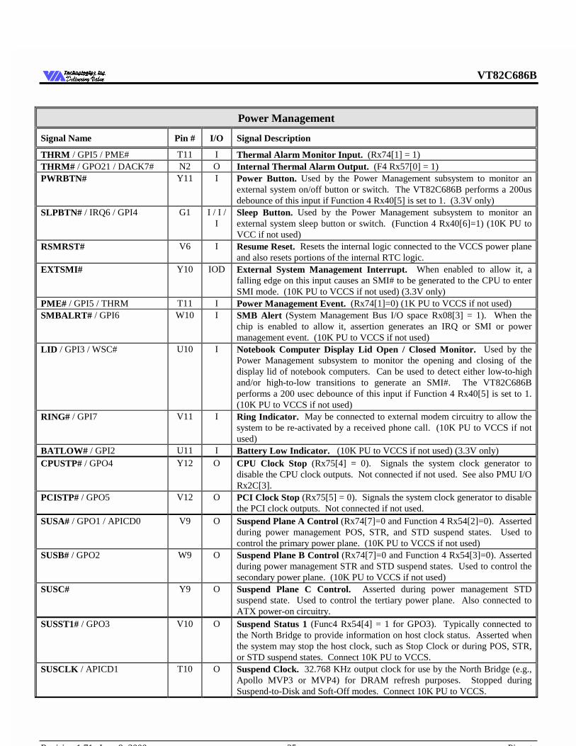
VT82C686B
Revision 1.71 June 9, 2000 -25- Pinouts
7HFKQRORJLHV ,QF'HOLYHULQJ 9DOXH'HOLYHULQJ 9DOXH
Power Management
Signal Name Pin # I/O Signal Description
THRM / GPI5 / PME# T11 I Thermal Alarm Monitor Input. (Rx74[1] = 1)THRM# / GPO21 / DACK7# N2 O Internal Thermal Alarm Output. (F4 Rx57[0] = 1)PWRBTN# Y11 I Power Button. Used by the Power Management subsystem to monitor an
external system on/off button or switch. The VT82C686B performs a 200usdebounce of this input if Function 4 Rx40[5] is set to 1. (3.3V only)
SLPBTN# / IRQ6 / GPI4 G1 I / I /I
Sleep Button. Used by the Power Management subsystem to monitor anexternal system sleep button or switch. (Function 4 Rx40[6]=1) (10K PU toVCC if not used)
RSMRST# V6 I Resume Reset. Resets the internal logic connected to the VCCS power planeand also resets portions of the internal RTC logic.
EXTSMI# Y10 IOD External System Management Interrupt. When enabled to allow it, afalling edge on this input causes an SMI# to be generated to the CPU to enterSMI mode. (10K PU to VCCS if not used) (3.3V only)
PME# / GPI5 / THRM T11 I Power Management Event. (Rx74[1]=0) (1K PU to VCCS if not used)SMBALRT# / GPI6 W10 I SMB Alert (System Management Bus I/O space Rx08[3] = 1). When the
chip is enabled to allow it, assertion generates an IRQ or SMI or powermanagement event. (10K PU to VCCS if not used)
LID / GPI3 / WSC# U10 I Notebook Computer Display Lid Open / Closed Monitor. Used by thePower Management subsystem to monitor the opening and closing of thedisplay lid of notebook computers. Can be used to detect either low-to-highand/or high-to-low transitions to generate an SMI#. The VT82C686Bperforms a 200 usec debounce of this input if Function 4 Rx40[5] is set to 1.(10K PU to VCCS if not used)
RING# / GPI7 V11 I Ring Indicator. May be connected to external modem circuitry to allow thesystem to be re-activated by a received phone call. (10K PU to VCCS if notused)
BATLOW# / GPI2 U11 I Battery Low Indicator. (10K PU to VCCS if not used) (3.3V only)CPUSTP# / GPO4 Y12 O CPU Clock Stop (Rx75[4] = 0). Signals the system clock generator to
disable the CPU clock outputs. Not connected if not used. See also PMU I/ORx2C[3].
PCISTP# / GPO5 V12 O PCI Clock Stop (Rx75[5] = 0). Signals the system clock generator to disablethe PCI clock outputs. Not connected if not used.
SUSA# / GPO1 / APICD0 V9 O Suspend Plane A Control (Rx74[7]=0 and Function 4 Rx54[2]=0). Assertedduring power management POS, STR, and STD suspend states. Used tocontrol the primary power plane. (10K PU to VCCS if not used)
SUSB# / GPO2 W9 O Suspend Plane B Control (Rx74[7]=0 and Function 4 Rx54[3]=0). Assertedduring power management STR and STD suspend states. Used to control thesecondary power plane. (10K PU to VCCS if not used)
SUSC# Y9 O Suspend Plane C Control. Asserted during power management STDsuspend state. Used to control the tertiary power plane. Also connected toATX power-on circuitry.
SUSST1# / GPO3 V10 O Suspend Status 1 (Func4 Rx54[4] = 1 for GPO3). Typically connected tothe North Bridge to provide information on host clock status. Asserted whenthe system may stop the host clock, such as Stop Clock or during POS, STR,or STD suspend states. Connect 10K PU to VCCS.
SUSCLK / APICD1 T10 O Suspend Clock. 32.768 KHz output clock for use by the North Bridge (e.g.,Apollo MVP3 or MVP4) for DRAM refresh purposes. Stopped duringSuspend-to-Disk and Soft-Off modes. Connect 10K PU to VCCS.
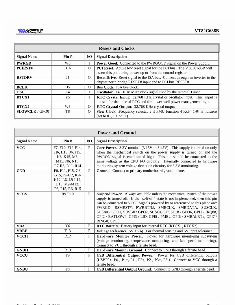
VT82C686B
Revision 1.71 June 9, 2000 -26- Pinouts
7HFKQRORJLHV ,QF'HOLYHULQJ 9DOXH'HOLYHULQJ 9DOXH
Resets and Clocks
Signal Name Pin # I/O Signal Description
PWRGD W6 I Power Good. Connected to the PWRGOOD signal on the Power Supply.PCIRST# B16 O PCI Reset. Active low reset signal for the PCI bus. The VT82C686B will
assert this pin during power-up or from the control register.RSTDRV J1 O Reset Drive. Reset signal to the ISA bus. Connect through an inverter to the
chipset north bridge RESET# input and to PCI bus RESET#.BCLK H5 O Bus Clock. ISA bus clock.OSC E4 I Oscillator. 14.31818 MHz clock signal used by the internal Timer.RTCX1 Y5 I RTC Crystal Input: 32.768 KHz crystal or oscillator input. This input is
used for the internal RTC and for power-well power management logic.RTCX2 W5 O RTC Crystal Output: 32.768 KHz crystal outputSLOWCLK / GPO0 T8 O Slow Clock. .Frequency selectable if PMU function 4 Rx54[1-0] is nonzero
(set to 01, 10, or 11).
Power and Ground
Signal Name Pin # I/O Signal Description
VCC F7, F10, F12-F14,H6, H15, J6, J15,
K6, K15, M6,M15, N6, N15,
R7-R8, R11, R14
P Core Power. 3.3V nominal (3.15V to 3.45V). This supply is turned on onlywhen the mechanical switch on the power supply is turned on and thePWRON signal is conditioned high. This pin should be connected to thesame voltage as the CPU I/O circuitry. Internally connected to hardwaremonitoring system voltage detection circuitry for 3.3V monitoring.
GND F6, F11, F15, G6,G15, J9-J12, K9-K12, L6, L9-L12,
L15, M9-M12,P6, P15, R6, R15
P Ground. Connect to primary motherboard ground plane.
VCCS R9-R10 P Suspend Power. Always available unless the mechanical switch of the powersupply is turned off. If the “soft-off” state is not implemented, then this pincan be connected to VCC. Signals powered by or referenced to this plane are:PWRGD, RSMRST#, PWRBTN#, SMBCLK, SMBDATA, SUSCLK,SUSA# / GPO1, SUSB# / GPO2, SUSC#, SUSST1# / GPO6, GPI1 / IRQ8#,GPI2 / BATLOW#, GPI3 / LID, GPI5 / PME#, GPI6 / SMBALRT#, GPI7 /RING#, GPO0
VBAT Y6 P RTC Battery. Battery input for internal RTC (RTCX1, RTCX2)VREF T13 P Voltage Reference (5V ±5%). For thermal sensing and 5V input tolerance.VCCH R12 P Hardware Monitor Power. Power for hardware monitoring subsystem
(voltage monitoring, temperature monitoring, and fan speed monitoring).Connect to VCC through a ferrite bead.
GNDH R13 P Hardware Monitor Ground. Connect to GND through a ferrite bead.VCCU F9 P USB Differential Output Power. Power for USB differential outputs
(USBP0+, P0-, P1+, P1-, P2+, P2-, P3+, P3-). Connect to VCC through aferrite bead.
GNDU F8 P USB Differential Output Ground. Connect to GND through a ferrite bead.

VT82C686B
Revision 1.71 June 9, 2000 -27- Register Overview
7HFKQRORJLHV ,QF'HOLYHULQJ 9DOXH'HOLYHULQJ 9DOXH
REGISTERS
Register Overview
The following tables summarize the configuration and I/Oregisters of the VT82C686B. These tables also document thepower-on default value (“Default”) and access type (“Acc”)for each register. Access type definitions used are RW(Read/Write), RO (Read/Only), “—” for reserved / used(essentially the same as RO), and RWC (or just WC) (Read /Write 1’s to Clear individual bits). Registers indicated as RWmay have some read/only bits that always read back a fixedvalue (usually 0 if unused); registers designated as RWC orWC may have some read-only or read write bits (seeindividual register descriptions for details).
Detailed register descriptions are provided in the followingsection of this document. All offset and default values areshown in hexadecimal unless otherwise indicated
Table 2. System I/O Map
Port Function Actual Port Decoding00-1F Master DMA Controller 0000 0000 000x nnnn20-3F Master Interrupt Controller 0000 0000 001x xxxn40-5F Timer / Counter 0000 0000 010x xxnn60-6F Keyboard Controller 0000 0000 0110 xnxn(60h) KBC Data 0000 0000 0110 x0x0(61h) Misc Functions & Spkr Ctrl 0000 0000 0110 xxx1(64h) KBC Command / Status 0000 0000 0110 x1x070-77 RTC/CMOS/NMI-Disable 0000 0000 0111 0nnn78-7F -available for system use- 0000 0000 0111 1xxx80 -reserved- (debug port) 0000 0000 1000 000081-8F DMA Page Registers 0000 0000 1000 nnnn90-91 -available for system use- 0000 0000 1001 000x92 System Control 0000 0000 1001 001093-9F -available for system use- 0000 0000 1001 nnnnA0-BF Slave Interrupt Controller 0000 0000 101x xxxnC0-DF Slave DMA Controller 0000 0000 110n nnnxE0-FF -available for system use- 0000 0000 111x xxxx
100-CF7 -available for system use*
CF8-CFB PCI Configuration Address 0000 1100 1111 10xxCFC-CFF PCI Configuration Data 0000 1100 1111 11xx
D00-FFFF -available for system use-
* On-Chip Super-I/O Functions – PC-Standard Port Addresses200-20F Game Port2E8-2EF COM42F8-2FF COM2378-37F Parallel Port (Standard & EPP)3E8-3EF COM33F0-3F1 Configuration Index / Data3F0-3F7 Floppy Controller3F8-3FF COM1778-77A Parallel Port (ECP Extensions) (Port 378+400)
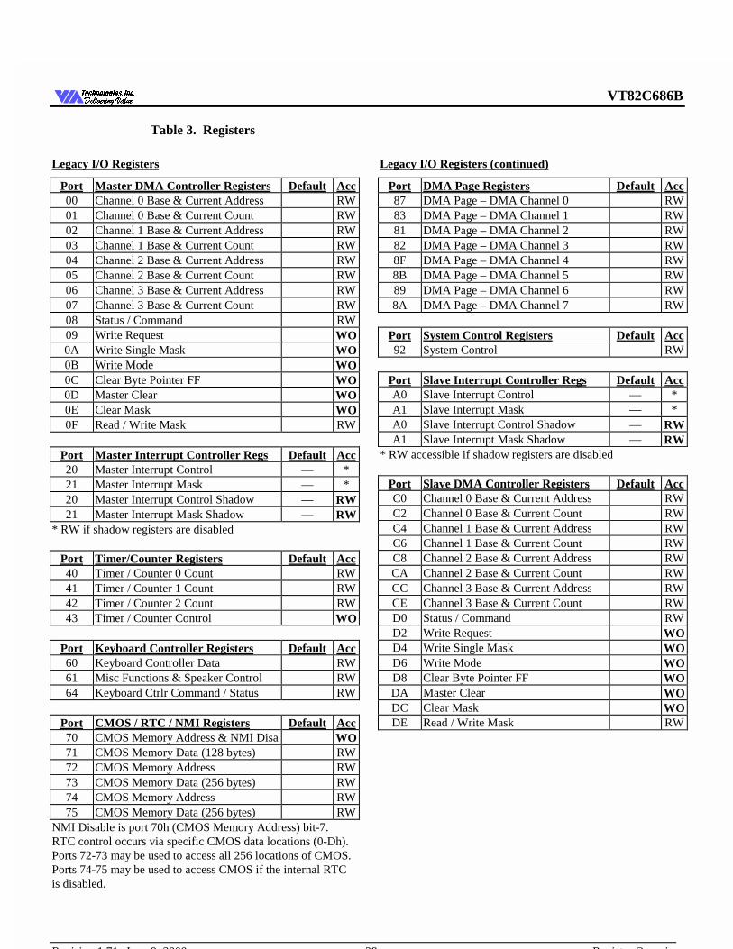
VT82C686B
Revision 1.71 June 9, 2000 -28- Register Overview
7HFKQRORJLHV ,QF'HOLYHULQJ 9DOXH'HOLYHULQJ 9DOXH
Table 3. Registers
Legacy I/O Registers
Port Master DMA Controller Registers Default Acc00 Channel 0 Base & Current Address RW01 Channel 0 Base & Current Count RW02 Channel 1 Base & Current Address RW03 Channel 1 Base & Current Count RW04 Channel 2 Base & Current Address RW05 Channel 2 Base & Current Count RW06 Channel 3 Base & Current Address RW07 Channel 3 Base & Current Count RW08 Status / Command RW09 Write Request WO0A Write Single Mask WO0B Write Mode WO0C Clear Byte Pointer FF WO0D Master Clear WO0E Clear Mask WO0F Read / Write Mask RW
Port Master Interrupt Controller Regs Default Acc20 Master Interrupt Control — *21 Master Interrupt Mask — *20 Master Interrupt Control Shadow — RW21 Master Interrupt Mask Shadow — RW
* RW if shadow registers are disabled
Port Timer/Counter Registers Default Acc40 Timer / Counter 0 Count RW41 Timer / Counter 1 Count RW42 Timer / Counter 2 Count RW43 Timer / Counter Control WO
Port Keyboard Controller Registers Default Acc60 Keyboard Controller Data RW61 Misc Functions & Speaker Control RW64 Keyboard Ctrlr Command / Status RW
Port CMOS / RTC / NMI Registers Default Acc70 CMOS Memory Address & NMI Disa WO71 CMOS Memory Data (128 bytes) RW72 CMOS Memory Address RW73 CMOS Memory Data (256 bytes) RW74 CMOS Memory Address RW75 CMOS Memory Data (256 bytes) RW
NMI Disable is port 70h (CMOS Memory Address) bit-7.RTC control occurs via specific CMOS data locations (0-Dh).Ports 72-73 may be used to access all 256 locations of CMOS.Ports 74-75 may be used to access CMOS if the internal RTCis disabled.
Legacy I/O Registers (continued)
Port DMA Page Registers Default Acc87 DMA Page – DMA Channel 0 RW83 DMA Page – DMA Channel 1 RW81 DMA Page – DMA Channel 2 RW82 DMA Page – DMA Channel 3 RW8F DMA Page – DMA Channel 4 RW8B DMA Page – DMA Channel 5 RW89 DMA Page – DMA Channel 6 RW8A DMA Page – DMA Channel 7 RW
Port System Control Registers Default Acc92 System Control RW
Port Slave Interrupt Controller Regs Default AccA0 Slave Interrupt Control — *A1 Slave Interrupt Mask — *A0 Slave Interrupt Control Shadow — RWA1 Slave Interrupt Mask Shadow — RW
* RW accessible if shadow registers are disabled
Port Slave DMA Controller Registers Default AccC0 Channel 0 Base & Current Address RWC2 Channel 0 Base & Current Count RWC4 Channel 1 Base & Current Address RWC6 Channel 1 Base & Current Count RWC8 Channel 2 Base & Current Address RWCA Channel 2 Base & Current Count RWCC Channel 3 Base & Current Address RWCE Channel 3 Base & Current Count RWD0 Status / Command RWD2 Write Request WOD4 Write Single Mask WOD6 Write Mode WOD8 Clear Byte Pointer FF WODA Master Clear WODC Clear Mask WODE Read / Write Mask RW
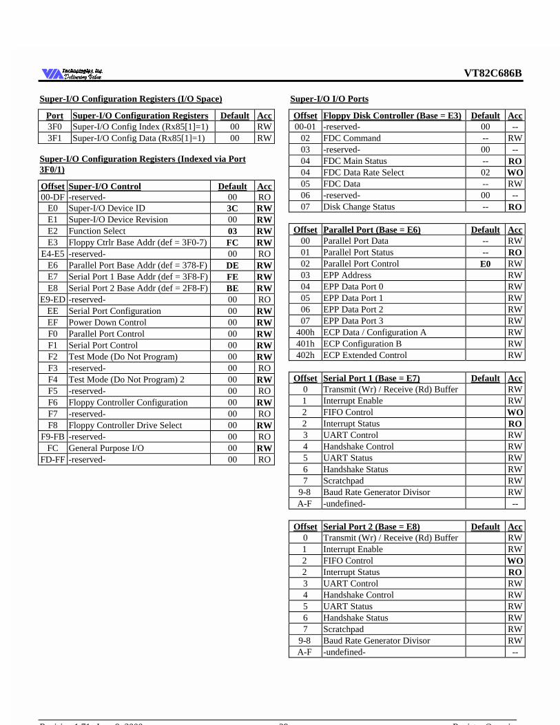
VT82C686B
Revision 1.71 June 9, 2000 -29- Register Overview
7HFKQRORJLHV ,QF'HOLYHULQJ 9DOXH'HOLYHULQJ 9DOXH
Super-I/O Configuration Registers (I/O Space)
Port Super-I/O Configuration Registers Default Acc3F0 Super-I/O Config Index (Rx85[1]=1) 00 RW3F1 Super-I/O Config Data (Rx85[1]=1) 00 RW
Super-I/O Configuration Registers (Indexed via Port3F0/1)
Offset Super-I/O Control Default Acc00-DF -reserved- 00 RO
E0 Super-I/O Device ID 3C RWE1 Super-I/O Device Revision 00 RWE2 Function Select 03 RWE3 Floppy Ctrlr Base Addr (def = 3F0-7) FC RW
E4-E5 -reserved- 00 ROE6 Parallel Port Base Addr (def = 378-F) DE RWE7 Serial Port 1 Base Addr (def = 3F8-F) FE RWE8 Serial Port 2 Base Addr (def = 2F8-F) BE RW
E9-ED -reserved- 00 ROEE Serial Port Configuration 00 RWEF Power Down Control 00 RWF0 Parallel Port Control 00 RWF1 Serial Port Control 00 RWF2 Test Mode (Do Not Program) 00 RWF3 -reserved- 00 ROF4 Test Mode (Do Not Program) 2 00 RWF5 -reserved- 00 ROF6 Floppy Controller Configuration 00 RWF7 -reserved- 00 ROF8 Floppy Controller Drive Select 00 RW
F9-FB -reserved- 00 ROFC General Purpose I/O 00 RW
FD-FF -reserved- 00 RO
Super-I/O I/O Ports
Offset Floppy Disk Controller (Base = E3) Default Acc00-01 -reserved- 00 --
02 FDC Command -- RW03 -reserved- 00 --04 FDC Main Status -- RO04 FDC Data Rate Select 02 WO05 FDC Data -- RW06 -reserved- 00 --07 Disk Change Status -- RO
Offset Parallel Port (Base = E6) Default Acc00 Parallel Port Data -- RW01 Parallel Port Status -- RO02 Parallel Port Control E0 RW03 EPP Address RW04 EPP Data Port 0 RW05 EPP Data Port 1 RW06 EPP Data Port 2 RW07 EPP Data Port 3 RW
400h ECP Data / Configuration A RW401h ECP Configuration B RW402h ECP Extended Control RW
Offset Serial Port 1 (Base = E7) Default Acc0 Transmit (Wr) / Receive (Rd) Buffer RW1 Interrupt Enable RW2 FIFO Control WO2 Interrupt Status RO3 UART Control RW4 Handshake Control RW5 UART Status RW6 Handshake Status RW7 Scratchpad RW
9-8 Baud Rate Generator Divisor RWA-F -undefined- --
Offset Serial Port 2 (Base = E8) Default Acc0 Transmit (Wr) / Receive (Rd) Buffer RW1 Interrupt Enable RW2 FIFO Control WO2 Interrupt Status RO3 UART Control RW4 Handshake Control RW5 UART Status RW6 Handshake Status RW7 Scratchpad RW
9-8 Baud Rate Generator Divisor RWA-F -undefined- --
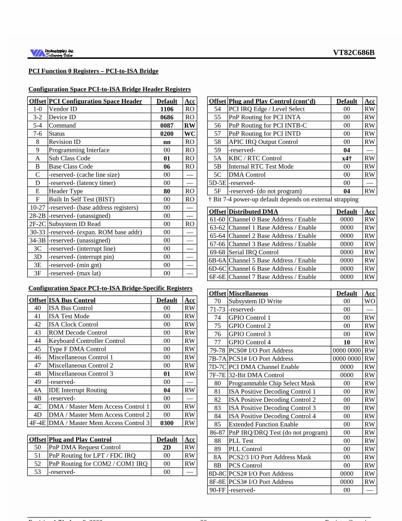
VT82C686B
Revision 1.71 June 9, 2000 -30- Register Overview
7HFKQRORJLHV ,QF'HOLYHULQJ 9DOXH'HOLYHULQJ 9DOXH
PCI Function 0 Registers – PCI-to-ISA Bridge
Configuration Space PCI-to-ISA Bridge Header Registers
Offset PCI Configuration Space Header Default Acc1-0 Vendor ID 1106 RO3-2 Device ID 0686 RO5-4 Command 0087 RW7-6 Status 0200 WC8 Revision ID nn RO9 Programming Interface 00 ROA Sub Class Code 01 ROB Base Class Code 06 ROC -reserved- (cache line size) 00 —D -reserved- (latency timer) 00 —E Header Type 80 ROF Built In Self Test (BIST) 00 RO
10-27 -reserved- (base address registers) 00 —28-2B -reserved- (unassigned) 00 —2F-2C Subsystem ID Read 00 RO30-33 -reserved- (expan. ROM base addr) 00 —34-3B -reserved- (unassigned) 00 —
3C -reserved- (interrupt line) 00 —3D -reserved- (interrupt pin) 00 —3E -reserved- (min gnt) 00 —3F -reserved- (max lat) 00 —
Configuration Space PCI-to-ISA Bridge-Specific Registers
Offset ISA Bus Control Default Acc40 ISA Bus Control 00 RW41 ISA Test Mode 00 RW42 ISA Clock Control 00 RW43 ROM Decode Control 00 RW44 Keyboard Controller Control 00 RW45 Type F DMA Control 00 RW46 Miscellaneous Control 1 00 RW47 Miscellaneous Control 2 00 RW48 Miscellaneous Control 3 01 RW49 -reserved- 00 —4A IDE Interrupt Routing 04 RW4B -reserved- 00 —4C DMA / Master Mem Access Control 1 00 RW4D DMA / Master Mem Access Control 2 00 RW
4F-4E DMA / Master Mem Access Control 3 0300 RW
Offset Plug and Play Control Default Acc50 PnP DMA Request Control 2D RW51 PnP Routing for LPT / FDC IRQ 00 RW52 PnP Routing for COM2 / COM1 IRQ 00 RW53 -reserved- 00 —
Offset Plug and Play Control (cont’d) Default Acc54 PCI IRQ Edge / Level Select 00 RW55 PnP Routing for PCI INTA 00 RW56 PnP Routing for PCI INTB-C 00 RW57 PnP Routing for PCI INTD 00 RW58 APIC IRQ Output Control 00 RW59 -reserved- 04 —5A KBC / RTC Control x4† RW5B Internal RTC Test Mode 00 RW5C DMA Control 00 RW
5D-5E -reserved- 00 —5F -reserved- (do not program) 04 RW
† Bit 7-4 power-up default depends on external strapping
Offset Distributed DMA Default Acc61-60 Channel 0 Base Address / Enable 0000 RW63-62 Channel 1 Base Address / Enable 0000 RW65-64 Channel 2 Base Address / Enable 0000 RW67-66 Channel 3 Base Address / Enable 0000 RW69-68 Serial IRQ Control 0000 RW6B-6A Channel 5 Base Address / Enable 0000 RW6D-6C Channel 6 Base Address / Enable 0000 RW6F-6E Channel 7 Base Address / Enable 0000 RW
Offset Miscellaneous Default Acc70 Subsystem ID Write 00 WO
71-73 -reserved- 00 —74 GPIO Control 1 00 RW75 GPIO Control 2 00 RW76 GPIO Control 3 00 RW77 GPIO Control 4 10 RW
79-78 PCS0# I/O Port Address 0000 0000 RW7B-7A PCS1# I/O Port Address 0000 0000 RW7D-7C PCI DMA Channel Enable 0000 RW7F-7E 32-Bit DMA Control 0000 RW
80 Programmable Chip Select Mask 00 RW81 ISA Positive Decoding Control 1 00 RW82 ISA Positive Decoding Control 2 00 RW83 ISA Positive Decoding Control 3 00 RW84 ISA Positive Decoding Control 4 00 RW85 Extended Function Enable 00 RW
86-87 PnP IRQ/DRQ Test (do not program) 00 RW88 PLL Test 00 RW89 PLL Control 00 RW8A PCS2/3 I/O Port Address Mask 00 RW8B PCS Control 00 RW
8D-8C PCS2# I/O Port Address 0000 RW8F-8E PCS3# I/O Port Address 0000 RW90-FF -reserved- 00 —
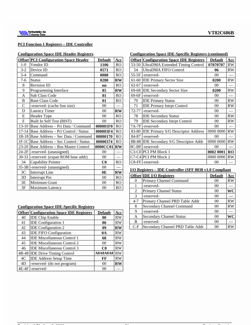
VT82C686B
Revision 1.71 June 9, 2000 -31- Register Overview
7HFKQRORJLHV ,QF'HOLYHULQJ 9DOXH'HOLYHULQJ 9DOXH
PCI Function 1 Registers – IDE Controller
Configuration Space IDE Header Registers
Offset PCI Configuration Space Header Default Acc1-0 Vendor ID 1106 RO3-2 Device ID 0571 RO5-4 Command 0080 RO7-6 Status 0280 RW8 Revision ID nn RO9 Programming Interface 85 RWA Sub Class Code 01 ROB Base Class Code 01 ROC -reserved- (cache line size) 00 —D Latency Timer 00 RWE Header Type 00 ROF Built In Self Test (BIST) 00 RO
13-10 Base Address – Pri Data / Command 000001F0 RO17-14 Base Address – Pri Control / Status 000003F4 RO1B-18 Base Address – Sec Data / Command 00000170 RO1F-1C Base Address – Sec Control / Status 00000374 RO23-20 Base Address – Bus Master Control 0000CC01 RW24-2F -reserved- (unassigned) 00 —30-33 -reserved- (expan ROM base addr) 00 —
34 Capability Pointer C0 RO35-3B -reserved- (unassigned) 00 —
3C Interrupt Line 0E RW3D Interrupt Pin 00 RO3E Minimum Grant 00 RO3F Maximum Latency 00 RO
Configuration Space IDE-Specific Registers
Offset Configuration Space IDE Registers Default Acc40 IDE Chip Enable 00 RW41 IDE Configuration 1 06 RW42 IDE Configuration 2 09 RW43 IDE FIFO Configuration 0A RW44 IDE Miscellaneous Control 1 68 RW45 IDE Miscellaneous Control 2 00 RW46 IDE Miscellaneous Control 3 C0 RW
4B-48 IDE Drive Timing Control A8A8A8A8 RW4C IDE Address Setup Time FF RW4D -reserved- (do not program) 00 RW
4E-4F -reserved- 00 —
Configuration Space IDE-Specific Registers (continued)
Offset Configuration Space IDE Registers Default Acc53-50 UltraDMA Extended Timing Control 07070707 RW
54 UltraDMA FIFO Control 06 RW55-5F -reserved- 00 —61-60 IDE Primary Sector Size 0200 RW62-67 -reserved- 00 —69-68 IDE Secondary Sector Size 0200 RW69-6F -reserved- 00 —
70 IDE Primary Status 00 RW71 IDE Primary Intrpt Control 00 RW
72-77 -reserved- 00 —78 IDE Secondary Status 00 RW79 IDE Secondary Intrpt Control 00 RW
7A-7F -reserved- 00 —83-80 IDE Primary S/G Descriptor Address 0000 0000 RW84-87 -reserved- 00 —8B-88 IDE Secondary S/G Descriptor Addr 0000 0000 RW8C-BF -reserved- 00 —C3-C0 PCI PM Block 1 0002 0001 ROC7-C4 PCI PM Block 2 0000 0000 RWC8-FF -reserved- 00 —
I/O Registers – IDE Controller (SFF 8038 v1.0 Compliant
Offset IDE I/O Registers Default Acc0 Primary Channel Command 00 RW1 -reserved- 00 —2 Primary Channel Status 00 WC3 -reserved- 00 —
4-7 Primary Channel PRD Table Addr 00 RW8 Secondary Channel Command 00 RW9 -reserved- 00 —A Secondary Channel Status 00 WCB -reserved- 00 —
C-F Secondary Channel PRD Table Addr 00 RW
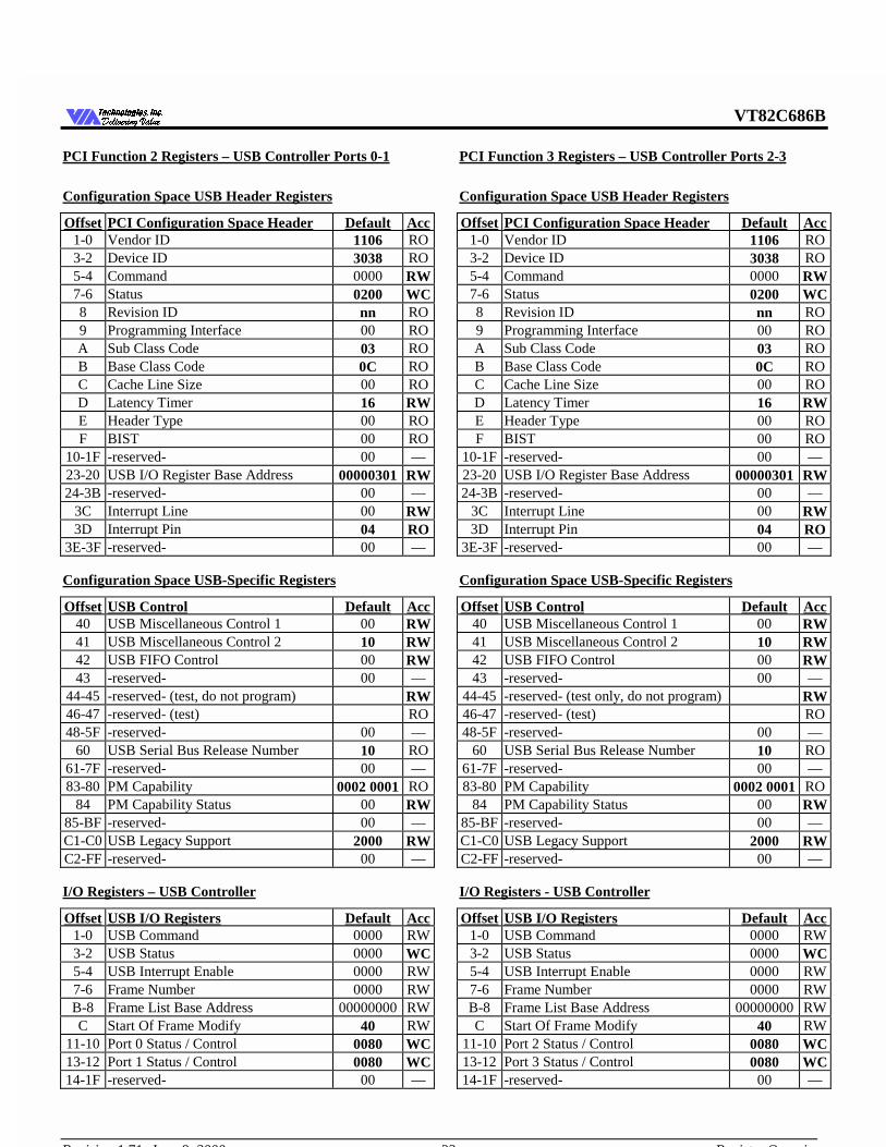
VT82C686B
Revision 1.71 June 9, 2000 -32- Register Overview
7HFKQRORJLHV ,QF'HOLYHULQJ 9DOXH'HOLYHULQJ 9DOXH
PCI Function 2 Registers – USB Controller Ports 0-1
Configuration Space USB Header Registers
Offset PCI Configuration Space Header Default Acc1-0 Vendor ID 1106 RO3-2 Device ID 3038 RO5-4 Command 0000 RW7-6 Status 0200 WC8 Revision ID nn RO9 Programming Interface 00 ROA Sub Class Code 03 ROB Base Class Code 0C ROC Cache Line Size 00 ROD Latency Timer 16 RWE Header Type 00 ROF BIST 00 RO
10-1F -reserved- 00 —23-20 USB I/O Register Base Address 00000301 RW24-3B -reserved- 00 —
3C Interrupt Line 00 RW3D Interrupt Pin 04 RO
3E-3F -reserved- 00 —
Configuration Space USB-Specific Registers
Offset USB Control Default Acc40 USB Miscellaneous Control 1 00 RW41 USB Miscellaneous Control 2 10 RW42 USB FIFO Control 00 RW43 -reserved- 00 —
44-45 -reserved- (test, do not program) RW46-47 -reserved- (test) RO48-5F -reserved- 00 —
60 USB Serial Bus Release Number 10 RO61-7F -reserved- 00 —83-80 PM Capability 0002 0001 RO
84 PM Capability Status 00 RW85-BF -reserved- 00 —C1-C0 USB Legacy Support 2000 RWC2-FF -reserved- 00 —
I/O Registers – USB Controller
Offset USB I/O Registers Default Acc1-0 USB Command 0000 RW3-2 USB Status 0000 WC5-4 USB Interrupt Enable 0000 RW7-6 Frame Number 0000 RWB-8 Frame List Base Address 00000000 RWC Start Of Frame Modify 40 RW
11-10 Port 0 Status / Control 0080 WC13-12 Port 1 Status / Control 0080 WC14-1F -reserved- 00 —
PCI Function 3 Registers – USB Controller Ports 2-3
Configuration Space USB Header Registers
Offset PCI Configuration Space Header Default Acc1-0 Vendor ID 1106 RO3-2 Device ID 3038 RO5-4 Command 0000 RW7-6 Status 0200 WC8 Revision ID nn RO9 Programming Interface 00 ROA Sub Class Code 03 ROB Base Class Code 0C ROC Cache Line Size 00 ROD Latency Timer 16 RWE Header Type 00 ROF BIST 00 RO
10-1F -reserved- 00 —23-20 USB I/O Register Base Address 00000301 RW24-3B -reserved- 00 —
3C Interrupt Line 00 RW3D Interrupt Pin 04 RO
3E-3F -reserved- 00 —
Configuration Space USB-Specific Registers
Offset USB Control Default Acc40 USB Miscellaneous Control 1 00 RW41 USB Miscellaneous Control 2 10 RW42 USB FIFO Control 00 RW43 -reserved- 00 —
44-45 -reserved- (test only, do not program) RW46-47 -reserved- (test) RO48-5F -reserved- 00 —
60 USB Serial Bus Release Number 10 RO61-7F -reserved- 00 —83-80 PM Capability 0002 0001 RO
84 PM Capability Status 00 RW85-BF -reserved- 00 —C1-C0 USB Legacy Support 2000 RWC2-FF -reserved- 00 —
I/O Registers - USB Controller
Offset USB I/O Registers Default Acc1-0 USB Command 0000 RW3-2 USB Status 0000 WC5-4 USB Interrupt Enable 0000 RW7-6 Frame Number 0000 RWB-8 Frame List Base Address 00000000 RWC Start Of Frame Modify 40 RW
11-10 Port 2 Status / Control 0080 WC13-12 Port 3 Status / Control 0080 WC14-1F -reserved- 00 —
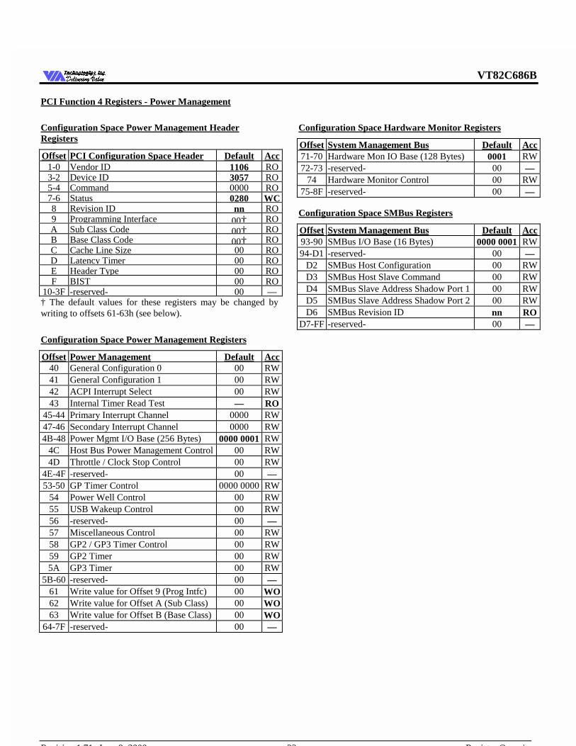
VT82C686B
Revision 1.71 June 9, 2000 -33- Register Overview
7HFKQRORJLHV ,QF'HOLYHULQJ 9DOXH'HOLYHULQJ 9DOXH
PCI Function 4 Registers - Power Management
Configuration Space Power Management HeaderRegisters
Offset PCI Configuration Space Header Default Acc1-0 Vendor ID 1106 RO3-2 Device ID 3057 RO5-4 Command 0000 RO7-6 Status 0280 WC8 Revision ID nn RO9 Programming Interface 00† ROA Sub Class Code 00† ROB Base Class Code 00† ROC Cache Line Size 00 ROD Latency Timer 00 ROE Header Type 00 ROF BIST 00 RO
10-3F -reserved- 00 —† The default values for these registers may be changed bywriting to offsets 61-63h (see below).
Configuration Space Power Management Registers
Offset Power Management Default Acc40 General Configuration 0 00 RW41 General Configuration 1 00 RW42 ACPI Interrupt Select 00 RW43 Internal Timer Read Test — RO
45-44 Primary Interrupt Channel 0000 RW47-46 Secondary Interrupt Channel 0000 RW4B-48 Power Mgmt I/O Base (256 Bytes) 0000 0001 RW
4C Host Bus Power Management Control 00 RW4D Throttle / Clock Stop Control 00 RW
4E-4F -reserved- 00 —53-50 GP Timer Control 0000 0000 RW
54 Power Well Control 00 RW55 USB Wakeup Control 00 RW56 -reserved- 00 —57 Miscellaneous Control 00 RW58 GP2 / GP3 Timer Control 00 RW59 GP2 Timer 00 RW5A GP3 Timer 00 RW
5B-60 -reserved- 00 —61 Write value for Offset 9 (Prog Intfc) 00 WO62 Write value for Offset A (Sub Class) 00 WO63 Write value for Offset B (Base Class) 00 WO
64-7F -reserved- 00 —
Configuration Space Hardware Monitor Registers
Offset System Management Bus Default Acc71-70 Hardware Mon IO Base (128 Bytes) 0001 RW72-73 -reserved- 00 —
74 Hardware Monitor Control 00 RW75-8F -reserved- 00 —
Configuration Space SMBus Registers
Offset System Management Bus Default Acc93-90 SMBus I/O Base (16 Bytes) 0000 0001 RW94-D1 -reserved- 00 —
D2 SMBus Host Configuration 00 RWD3 SMBus Host Slave Command 00 RWD4 SMBus Slave Address Shadow Port 1 00 RWD5 SMBus Slave Address Shadow Port 2 00 RWD6 SMBus Revision ID nn RO
D7-FF -reserved- 00 —
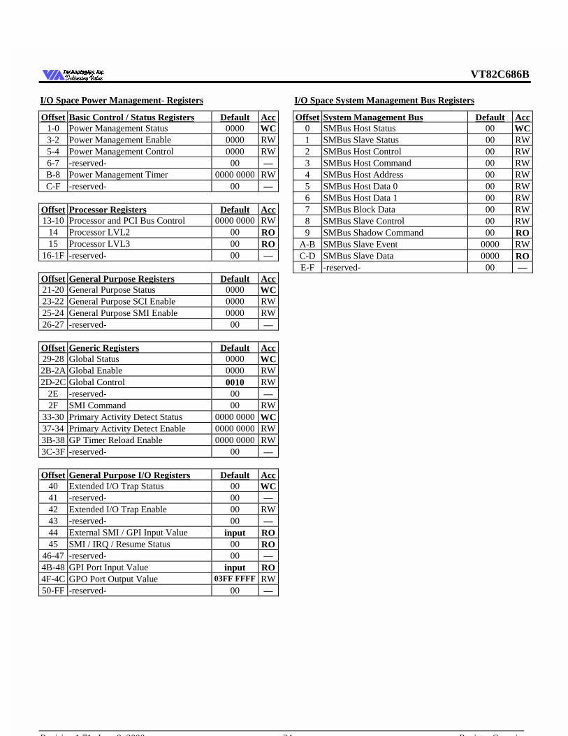
VT82C686B
Revision 1.71 June 9, 2000 -34- Register Overview
7HFKQRORJLHV ,QF'HOLYHULQJ 9DOXH'HOLYHULQJ 9DOXH
I/O Space Power Management- Registers
Offset Basic Control / Status Registers Default Acc1-0 Power Management Status 0000 WC3-2 Power Management Enable 0000 RW5-4 Power Management Control 0000 RW6-7 -reserved- 00 —B-8 Power Management Timer 0000 0000 RWC-F -reserved- 00 —
Offset Processor Registers Default Acc13-10 Processor and PCI Bus Control 0000 0000 RW
14 Processor LVL2 00 RO15 Processor LVL3 00 RO
16-1F -reserved- 00 —
Offset General Purpose Registers Default Acc21-20 General Purpose Status 0000 WC23-22 General Purpose SCI Enable 0000 RW25-24 General Purpose SMI Enable 0000 RW26-27 -reserved- 00 —
Offset Generic Registers Default Acc29-28 Global Status 0000 WC2B-2A Global Enable 0000 RW2D-2C Global Control 0010 RW
2E -reserved- 00 —2F SMI Command 00 RW
33-30 Primary Activity Detect Status 0000 0000 WC37-34 Primary Activity Detect Enable 0000 0000 RW3B-38 GP Timer Reload Enable 0000 0000 RW3C-3F -reserved- 00 —
Offset General Purpose I/O Registers Default Acc40 Extended I/O Trap Status 00 WC41 -reserved- 00 —42 Extended I/O Trap Enable 00 RW43 -reserved- 00 —44 External SMI / GPI Input Value input RO45 SMI / IRQ / Resume Status 00 RO
46-47 -reserved- 00 —4B-48 GPI Port Input Value input RO4F-4C GPO Port Output Value 03FF FFFF RW50-FF -reserved- 00 —
I/O Space System Management Bus Registers
Offset System Management Bus Default Acc0 SMBus Host Status 00 WC1 SMBus Slave Status 00 RW2 SMBus Host Control 00 RW3 SMBus Host Command 00 RW4 SMBus Host Address 00 RW5 SMBus Host Data 0 00 RW6 SMBus Host Data 1 00 RW7 SMBus Block Data 00 RW8 SMBus Slave Control 00 RW9 SMBus Shadow Command 00 RO
A-B SMBus Slave Event 0000 RWC-D SMBus Slave Data 0000 ROE-F -reserved- 00 —
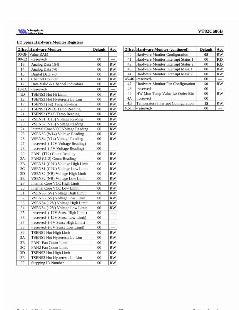
VT82C686B
Revision 1.71 June 9, 2000 -35- Register Overview
7HFKQRORJLHV ,QF'HOLYHULQJ 9DOXH'HOLYHULQJ 9DOXH
I/O Space Hardware Monitor Registers
Offset Hardware Monitor Default Acc00-3F Value RAM00-12 -reserved- 00 —
13 Analog Data 15-8 00 RW14 Analog Data 7-0 00 RW15 Digital Data 7-0 00 RW16 Channel Counter 00 RW17 Data Valid & Channel Indicators 00 RW
18-1C -reserved- 00 —1D TSENS3 Hot Hi Limit 00 RW1E TSENS3 Hot Hysteresis Lo Lim 00 RW1F TSENS3 (Int) Temp Reading 00 RW20 TSENS1 (W13) Temp Reading 00 RW21 TSENS2 (Y13) Temp Reading 00 RW22 VSENS1 (U13) Voltage Reading 00 RW23 VSENS2 (V13) Voltage Reading 00 RW24 Internal Core VCC Voltage Reading 00 RW25 VSENS3 (W14) Voltage Reading 00 RW26 VSENS4 (Y14) Voltage Reading 00 RW27 -reserved- (-12V Voltage Reading) 00 —28 -reserved- (-5V Voltage Reading) 00 —29 FAN1 (T12) Count Reading 00 RW2A FAN2 (U12) Count Reading 00 RW2B VSENS1 (CPU) Voltage High Limit 00 RW2C VSENS1 (CPU) Voltage Low Limit 00 RW2D VSENS2 (NB) Voltage High Limit 00 RW2E VSENS2 (NB) Voltage Low Limit 00 RW2F Internal Core VCC High Limit 00 RW30 Internal Core VCC Low Limit 00 RW31 VSENS3 (5V) Voltage High Limit 00 RW32 VSENS3 (5V) Voltage Low Limit 00 RW33 VSENS4 (12V) Voltage High Limit 00 RW34 VSENS4 (12V) Voltage Low Limit 00 RW35 -reserved- (-12V Sense High Limit) 00 —36 -reserved- (-12V Sense Low Limit) 00 —37 -reserved- (-5V Sense High Limit) 00 —38 -reserved- (-5V Sense Low Limit) 00 —39 TSENS1 Hot High Limit 00 RW3A TSENS1 Hot Hysteresis Lo Lim 00 RW3B FAN1 Fan Count Limit 00 RW3C FAN2 Fan Count Limit 00 RW3D TSENS2 Hot High Limit 00 RW3E TSENS2 Hot Hysteresis Lo Lim 00 RW3F Stepping ID Number 00 RW
Offset Hardware Monitor (continued) Default Acc40 Hardware Monitor Configuration 08 RW41 Hardware Monitor Interrupt Status 1 00 RO42 Hardware Monitor Interrupt Status 2 00 RO43 Hardware Monitor Interrupt Mask 1 00 RW44 Hardware Monitor Interrupt Mask 2 00 RW
45-46 -reserved- 00 —47 Hardware Monitor Fan Configuration 50 RW48 -reserved- 00 —49 HW Mon Temp Value Lo-Order Bits 00 RW4A -reserved- 00 —4B Temperature Interrupt Configuration 15 RW
4C-FF -reserved- 00 —
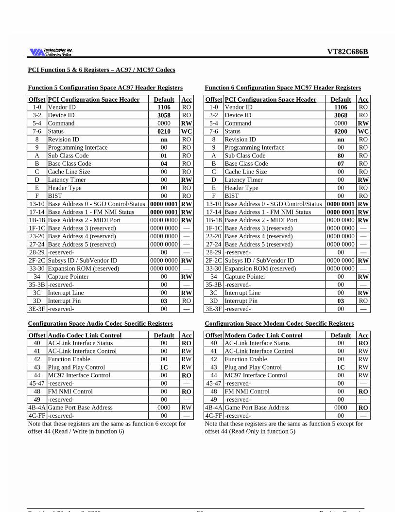
VT82C686B
Revision 1.71 June 9, 2000 -36- Register Overview
7HFKQRORJLHV ,QF'HOLYHULQJ 9DOXH'HOLYHULQJ 9DOXH
PCI Function 5 & 6 Registers – AC97 / MC97 Codecs
Function 5 Configuration Space AC97 Header Registers
Offset PCI Configuration Space Header Default Acc1-0 Vendor ID 1106 RO3-2 Device ID 3058 RO5-4 Command 0000 RW7-6 Status 0210 WC8 Revision ID nn RO9 Programming Interface 00 ROA Sub Class Code 01 ROB Base Class Code 04 ROC Cache Line Size 00 ROD Latency Timer 00 RWE Header Type 00 ROF BIST 00 RO
13-10 Base Address 0 - SGD Control/Status 0000 0001 RW17-14 Base Address 1 - FM NMI Status 0000 0001 RW1B-18 Base Address 2 - MIDI Port 0000 0000 RW1F-1C Base Address 3 (reserved) 0000 0000 —23-20 Base Address 4 (reserved) 0000 0000 —27-24 Base Address 5 (reserved) 0000 0000 —28-29 -reserved- 00 —2F-2C Subsys ID / SubVendor ID 0000 0000 RW33-30 Expansion ROM (reserved) 0000 0000 —
34 Capture Pointer 00 RW35-3B -reserved- 00 —
3C Interrupt Line 00 RW3D Interrupt Pin 03 RO
3E-3F -reserved- 00 —
Configuration Space Audio Codec-Specific Registers
Offset Audio Codec Link Control Default Acc40 AC-Link Interface Status 00 RO41 AC-Link Interface Control 00 RW42 Function Enable 00 RW43 Plug and Play Control 1C RW44 MC97 Interface Control 00 RO
45-47 -reserved- 00 —48 FM NMI Control 00 RO49 -reserved- 00 —
4B-4A Game Port Base Address 0000 RW4C-FF -reserved- 00 —Note that these registers are the same as function 6 except foroffset 44 (Read / Write in function 6)
Function 6 Configuration Space MC97 Header Registers
Offset PCI Configuration Space Header Default Acc1-0 Vendor ID 1106 RO3-2 Device ID 3068 RO5-4 Command 0000 RW7-6 Status 0200 WC8 Revision ID nn RO9 Programming Interface 00 ROA Sub Class Code 80 ROB Base Class Code 07 ROC Cache Line Size 00 ROD Latency Timer 00 RWE Header Type 00 ROF BIST 00 RO
13-10 Base Address 0 - SGD Control/Status 0000 0001 RW17-14 Base Address 1 - FM NMI Status 0000 0001 RW1B-18 Base Address 2 - MIDI Port 0000 0000 RW1F-1C Base Address 3 (reserved) 0000 0000 —23-20 Base Address 4 (reserved) 0000 0000 —27-24 Base Address 5 (reserved) 0000 0000 —28-29 -reserved- 00 —2F-2C Subsys ID / SubVendor ID 0000 0000 RW33-30 Expansion ROM (reserved) 0000 0000 —
34 Capture Pointer 00 RW35-3B -reserved- 00 —
3C Interrupt Line 00 RW3D Interrupt Pin 03 RO
3E-3F -reserved- 00 —
Configuration Space Modem Codec-Specific Registers
Offset Modem Codec Link Control Default Acc40 AC-Link Interface Status 00 RO41 AC-Link Interface Control 00 RW42 Function Enable 00 RW43 Plug and Play Control 1C RW44 MC97 Interface Control 00 RW
45-47 -reserved- 00 —48 FM NMI Control 00 RO49 -reserved- 00 —
4B-4A Game Port Base Address 0000 RO4C-FF -reserved- 00 —Note that these registers are the same as function 5 except foroffset 44 (Read Only in function 5)
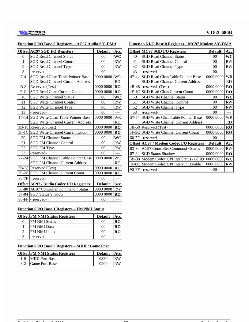
VT82C686B
Revision 1.71 June 9, 2000 -37- Register Overview
7HFKQRORJLHV ,QF'HOLYHULQJ 9DOXH'HOLYHULQJ 9DOXH
Function 5 I/O Base 0 Registers – AC97 Audio S/G DMA
Offset AC97 SGD I/O Registers Default Acc0 SGD Read Channel Status 00 WC1 SGD Read Channel Control 00 RW2 SGD Read Channel Type 00 RW3 -reserved- 00 —
7-4 SGD Read Chan Table Pointer BaseSGD Read Channel Current Address
0000 0000 WRRD
B-8 Reserved (Test) 0000 0000 ROF-C SGD Read Chan Current Count 0000 0000 RO10 SGD Write Channel Status 00 WC11 SGD Write Channel Control 00 RW12 SGD Write Channel Type 00 RW13 -reserved- 00 —
17-14 SGD Write Chan Table Pointer BaseSGD Write Channel Current Address
0000 0000 WRRD
1B-18 Reserved (Test) 0000 0000 RO1F-1C SGD Write Channel Current Count 0000 0000 RO
20 SGD FM Channel Status 00 WC21 SGD FM Channel Control 00 RW22 SGD FM Type 00 RW23 -reserved- 00 —
27-24 SGD FM Channel Table Pointer BaseSGD FM Channel Current Address
0000 0000 WRRD
2B-28 Reserved (Test) 0000 0000 RO2F-2C SGD FM Channel Current Count 0000 0000 RO30-7F -reserved- 00 —Offset AC97 / Audio Codec I/O Registers Default Acc83-80 AC97 Controller Command / Status 0000 0000 RW87-84 SGD Status Shadow 0000 0000 RO88-FF -reserved- 00 —
Function 5 I/O Base 1 Registers – FM NMI Status
Offset FM NMI Status Registers Default Acc0 FM NMI Status 00 RO1 FM NMI Data 00 RO2 FM NMI Index 00 RO3 -reserved- 00 —
Function 5 I/O Base 2 Registers – MIDI / Game Port
Offset FM NMI Status Registers Default Acc1-0 MIDI Port Base 0330 RW3-2 Game Port Base 0200 RW
Function 6 I/O Base 0 Registers – MC97 Modem S/G DMA
Offset MC97 SGD I/O Registers Default Acc40 SGD Read Channel Status 00 WC41 SGD Read Channel Control 00 RW42 SGD Read Channel Type 00 RW43 -reserved- 00 —
47-44 SGD Read Chan Table Pointer BaseSGD Read Channel Current Address
0000 0000 WRRD
4B-48 -reserved- (Test) 0000 0000 RO4F-4C SGD Read Chan Current Count 0000 0000 RO
50 SGD Write Channel Status 00 WC51 SGD Write Channel Control 00 RW52 SGD Write Channel Type 00 RW53 -reserved- 00 —
57-54 SGD Write Chan Table Pointer BaseSGD Write Channel Current Address
0000 0000 WRRD
5B-58 Reserved (Test) 0000 0000 RO5F-5C SGD Write Channel Current Count 0000 0000 RO60-7F -reserved- 00 —Offset AC97 / Modem Codec I/O Registers Default Acc83-80 AC97 Controller Command / Status 0000 0000 RW87-84 SGD Status Shadow 0000 0000 RO8B-88 Modem Codec GPI Intr Status / GPIO 0000 0000 WC8F-8C Modem Codec GPI Interrupt Enable 0000 0000 RW90-FF -reserved- 00 —
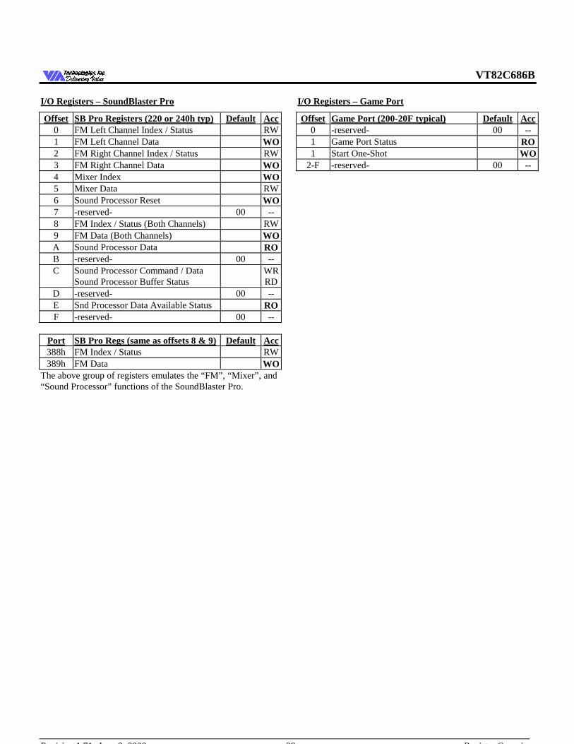
VT82C686B
Revision 1.71 June 9, 2000 -38- Register Overview
7HFKQRORJLHV ,QF'HOLYHULQJ 9DOXH'HOLYHULQJ 9DOXH
I/O Registers – SoundBlaster Pro
Offset SB Pro Registers (220 or 240h typ) Default Acc0 FM Left Channel Index / Status RW1 FM Left Channel Data WO2 FM Right Channel Index / Status RW3 FM Right Channel Data WO4 Mixer Index WO5 Mixer Data RW6 Sound Processor Reset WO7 -reserved- 00 --8 FM Index / Status (Both Channels) RW9 FM Data (Both Channels) WOA Sound Processor Data ROB -reserved- 00 --C Sound Processor Command / Data
Sound Processor Buffer StatusWRRD
D -reserved- 00 --E Snd Processor Data Available Status ROF -reserved- 00 --
Port SB Pro Regs (same as offsets 8 & 9) Default Acc388h FM Index / Status RW389h FM Data WO
The above group of registers emulates the “FM”, “Mixer”, and“Sound Processor” functions of the SoundBlaster Pro.
I/O Registers – Game Port
Offset Game Port (200-20F typical) Default Acc0 -reserved- 00 --1 Game Port Status RO1 Start One-Shot WO
2-F -reserved- 00 --
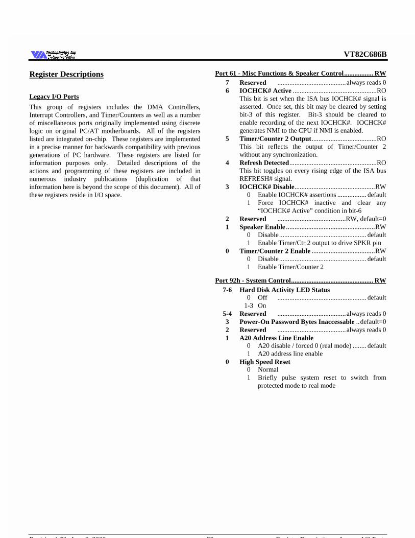
VT82C686B
Revision 1.71 June 9, 2000 -39- Register Descriptions - Legacy I/O Ports
7HFKQRORJLHV ,QF'HOLYHULQJ 9DOXH'HOLYHULQJ 9DOXH
Register Descriptions
Legacy I/O Ports
This group of registers includes the DMA Controllers,Interrupt Controllers, and Timer/Counters as well as a numberof miscellaneous ports originally implemented using discretelogic on original PC/AT motherboards. All of the registerslisted are integrated on-chip. These registers are implementedin a precise manner for backwards compatibility with previousgenerations of PC hardware. These registers are listed forinformation purposes only. Detailed descriptions of theactions and programming of these registers are included innumerous industry publications (duplication of thatinformation here is beyond the scope of this document). All ofthese registers reside in I/O space.
Port 61 - Misc Functions & Speaker Control ................. RW7 Reserved ........................................always reads 06 IOCHCK# Active .................................................RO
This bit is set when the ISA bus IOCHCK# signal isasserted. Once set, this bit may be cleared by settingbit-3 of this register. Bit-3 should be cleared toenable recording of the next IOCHCK#. IOCHCK#generates NMI to the CPU if NMI is enabled.
5 Timer/Counter 2 Output......................................ROThis bit reflects the output of Timer/Counter 2without any synchronization.
4 Refresh Detected...................................................ROThis bit toggles on every rising edge of the ISA busREFRESH# signal.
3 IOCHCK# Disable...............................................RW0 Enable IOCHCK# assertions ................. default1 Force IOCHCK# inactive and clear any
“IOCHCK# Active” condition in bit-62 Reserved ........................................RW, default=01 Speaker Enable ....................................................RW
0 Disable................................................... default1 Enable Timer/Ctr 2 output to drive SPKR pin
0 Timer/Counter 2 Enable .....................................RW0 Disable................................................... default1 Enable Timer/Counter 2
Port 92h - System Control ................................................ RW7-6 Hard Disk Activity LED Status
0 Off .................................................... default1-3 On
5-4 Reserved ........................................always reads 03 Power-On Password Bytes Inaccessable ..default=02 Reserved ........................................always reads 01 A20 Address Line Enable
0 A20 disable / forced 0 (real mode) ........ default1 A20 address line enable
0 High Speed Reset0 Normal1 Briefly pulse system reset to switch from
protected mode to real mode
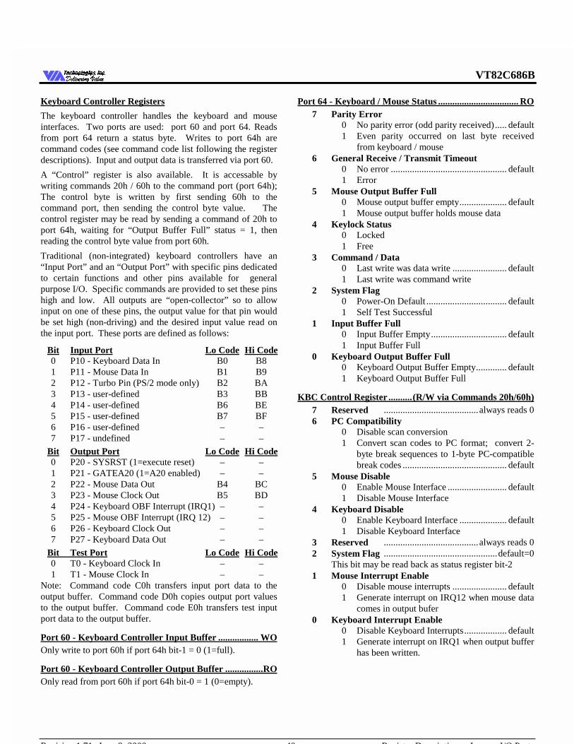
VT82C686B
Revision 1.71 June 9, 2000 -40- Register Descriptions - Legacy I/O Ports
7HFKQRORJLHV ,QF'HOLYHULQJ 9DOXH'HOLYHULQJ 9DOXH
Keyboard Controller Registers
The keyboard controller handles the keyboard and mouseinterfaces. Two ports are used: port 60 and port 64. Readsfrom port 64 return a status byte. Writes to port 64h arecommand codes (see command code list following the registerdescriptions). Input and output data is transferred via port 60.
A “Control” register is also available. It is accessable bywriting commands 20h / 60h to the command port (port 64h);The control byte is written by first sending 60h to thecommand port, then sending the control byte value. Thecontrol register may be read by sending a command of 20h toport 64h, waiting for “Output Buffer Full” status = 1, thenreading the control byte value from port 60h.
Traditional (non-integrated) keyboard controllers have an“Input Port” and an “Output Port” with specific pins dedicatedto certain functions and other pins available for generalpurpose I/O. Specific commands are provided to set these pinshigh and low. All outputs are “open-collector” so to allowinput on one of these pins, the output value for that pin wouldbe set high (non-driving) and the desired input value read onthe input port. These ports are defined as follows:
Bit Input Port Lo Code Hi Code0 P10 - Keyboard Data In B0 B81 P11 - Mouse Data In B1 B92 P12 - Turbo Pin (PS/2 mode only) B2 BA3 P13 - user-defined B3 BB4 P14 - user-defined B6 BE5 P15 - user-defined B7 BF6 P16 - user-defined – –7 P17 - undefined – –
Bit Output Port Lo Code Hi Code0 P20 - SYSRST (1=execute reset) – –1 P21 - GATEA20 (1=A20 enabled) – –2 P22 - Mouse Data Out B4 BC3 P23 - Mouse Clock Out B5 BD4 P24 - Keyboard OBF Interrupt (IRQ1) – –5 P25 - Mouse OBF Interrupt (IRQ 12) – –6 P26 - Keyboard Clock Out – –7 P27 - Keyboard Data Out – –
Bit Test Port Lo Code Hi Code0 T0 - Keyboard Clock In – –1 T1 - Mouse Clock In – –
Note: Command code C0h transfers input port data to theoutput buffer. Command code D0h copies output port valuesto the output buffer. Command code E0h transfers test inputport data to the output buffer.
Port 60 - Keyboard Controller Input Buffer ................. WOOnly write to port 60h if port 64h bit-1 = 0 (1=full).
Port 60 - Keyboard Controller Output Buffer ................ ROOnly read from port 60h if port 64h bit-0 = 1 (0=empty).
Port 64 - Keyboard / Mouse Status .................................. RO7 Parity Error
0 No parity error (odd parity received)..... default1 Even parity occurred on last byte received
from keyboard / mouse6 General Receive / Transmit Timeout
0 No error ................................................. default1 Error
5 Mouse Output Buffer Full0 Mouse output buffer empty.................... default1 Mouse output buffer holds mouse data
4 Keylock Status0 Locked1 Free
3 Command / Data0 Last write was data write ....................... default1 Last write was command write
2 System Flag0 Power-On Default .................................. default1 Self Test Successful
1 Input Buffer Full0 Input Buffer Empty................................ default1 Input Buffer Full
0 Keyboard Output Buffer Full0 Keyboard Output Buffer Empty............. default1 Keyboard Output Buffer Full
KBC Control Register .......... (R/W via Commands 20h/60h)7 Reserved ........................................always reads 06 PC Compatibility
0 Disable scan conversion1 Convert scan codes to PC format; convert 2-
byte break sequences to 1-byte PC-compatiblebreak codes ............................................ default
5 Mouse Disable0 Enable Mouse Interface ......................... default1 Disable Mouse Interface
4 Keyboard Disable0 Enable Keyboard Interface .................... default1 Disable Keyboard Interface
3 Reserved ........................................always reads 02 System Flag ................................................default=0
This bit may be read back as status register bit-21 Mouse Interrupt Enable
0 Disable mouse interrupts ....................... default1 Generate interrupt on IRQ12 when mouse data
comes in output bufer0 Keyboard Interrupt Enable
0 Disable Keyboard Interrupts.................. default1 Generate interrupt on IRQ1 when output buffer
has been written.
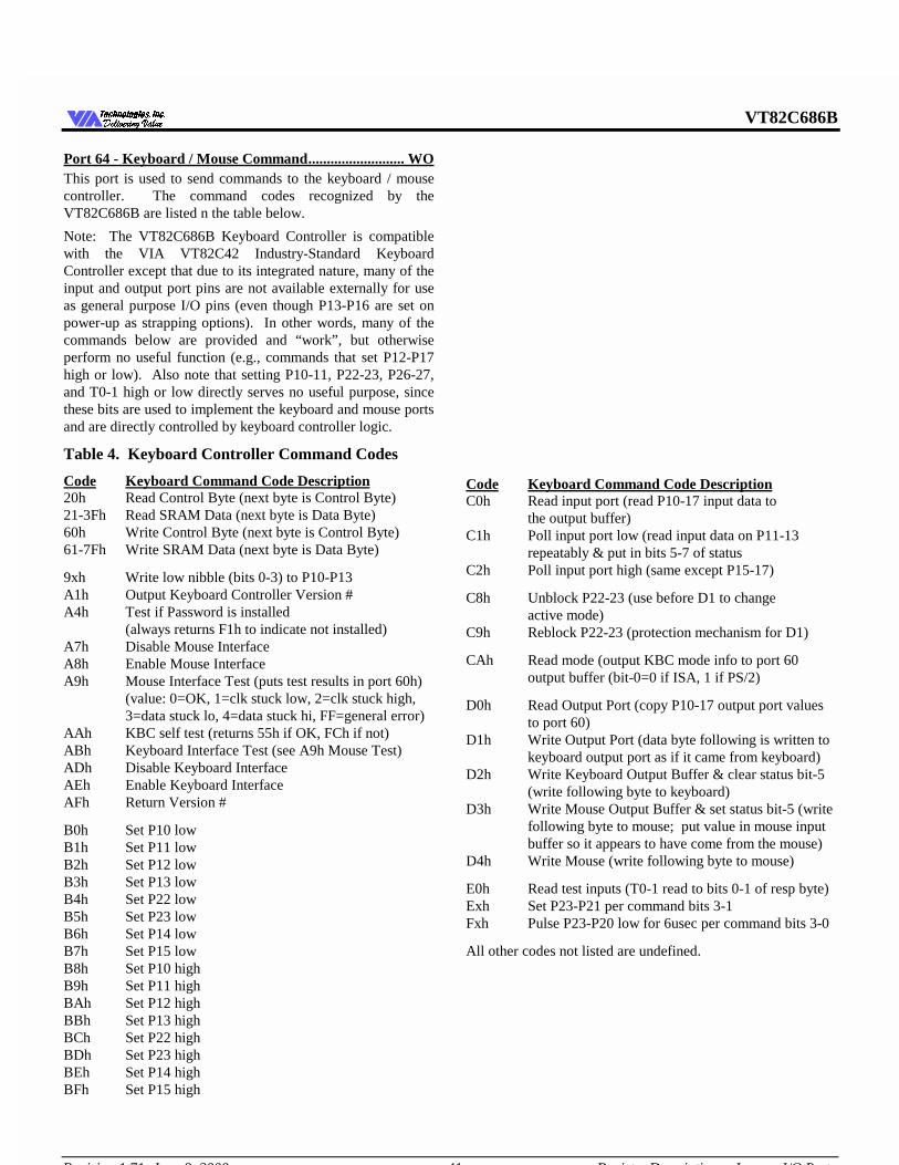
VT82C686B
Revision 1.71 June 9, 2000 -41- Register Descriptions - Legacy I/O Ports
7HFKQRORJLHV ,QF'HOLYHULQJ 9DOXH'HOLYHULQJ 9DOXH
Port 64 - Keyboard / Mouse Command .......................... WOThis port is used to send commands to the keyboard / mousecontroller. The command codes recognized by theVT82C686B are listed n the table below.
Note: The VT82C686B Keyboard Controller is compatiblewith the VIA VT82C42 Industry-Standard KeyboardController except that due to its integrated nature, many of theinput and output port pins are not available externally for useas general purpose I/O pins (even though P13-P16 are set onpower-up as strapping options). In other words, many of thecommands below are provided and “work”, but otherwiseperform no useful function (e.g., commands that set P12-P17high or low). Also note that setting P10-11, P22-23, P26-27,and T0-1 high or low directly serves no useful purpose, sincethese bits are used to implement the keyboard and mouse portsand are directly controlled by keyboard controller logic.
Table 4. Keyboard Controller Command Codes
Code Keyboard Command Code Description20h Read Control Byte (next byte is Control Byte)21-3Fh Read SRAM Data (next byte is Data Byte)60h Write Control Byte (next byte is Control Byte)61-7Fh Write SRAM Data (next byte is Data Byte)
9xh Write low nibble (bits 0-3) to P10-P13A1h Output Keyboard Controller Version #A4h Test if Password is installed
(always returns F1h to indicate not installed)A7h Disable Mouse InterfaceA8h Enable Mouse InterfaceA9h Mouse Interface Test (puts test results in port 60h)
(value: 0=OK, 1=clk stuck low, 2=clk stuck high,3=data stuck lo, 4=data stuck hi, FF=general error)
AAh KBC self test (returns 55h if OK, FCh if not)ABh Keyboard Interface Test (see A9h Mouse Test)ADh Disable Keyboard InterfaceAEh Enable Keyboard InterfaceAFh Return Version #
B0h Set P10 lowB1h Set P11 lowB2h Set P12 lowB3h Set P13 lowB4h Set P22 lowB5h Set P23 lowB6h Set P14 lowB7h Set P15 lowB8h Set P10 highB9h Set P11 highBAh Set P12 highBBh Set P13 highBCh Set P22 highBDh Set P23 highBEh Set P14 highBFh Set P15 high
Code Keyboard Command Code DescriptionC0h Read input port (read P10-17 input data to
the output buffer)C1h Poll input port low (read input data on P11-13
repeatably & put in bits 5-7 of statusC2h Poll input port high (same except P15-17)
C8h Unblock P22-23 (use before D1 to changeactive mode)
C9h Reblock P22-23 (protection mechanism for D1)
CAh Read mode (output KBC mode info to port 60output buffer (bit-0=0 if ISA, 1 if PS/2)
D0h Read Output Port (copy P10-17 output port valuesto port 60)
D1h Write Output Port (data byte following is written tokeyboard output port as if it came from keyboard)
D2h Write Keyboard Output Buffer & clear status bit-5(write following byte to keyboard)
D3h Write Mouse Output Buffer & set status bit-5 (writefollowing byte to mouse; put value in mouse inputbuffer so it appears to have come from the mouse)
D4h Write Mouse (write following byte to mouse)
E0h Read test inputs (T0-1 read to bits 0-1 of resp byte)Exh Set P23-P21 per command bits 3-1Fxh Pulse P23-P20 low for 6usec per command bits 3-0
All other codes not listed are undefined.
VT82C686B
Revision 1.71 June 9, 2000 -42- Register Descriptions - Legacy I/O Ports
7HFKQRORJLHV ,QF'HOLYHULQJ 9DOXH'HOLYHULQJ 9DOXH
DMA Controller I/O Registers
Ports 00-0F - Master DMA ControllerChannels 0-3 of the Master DMA Controller control SystemDMA Channels 0-3. There are 16 Master DMA Controllerregisters:
I/O Address Bits 15-0 Register Name0000 0000 000x 0000 Ch 0 Base / Current Address RW0000 0000 000x 0001 Ch 0 Base / Current Count RW0000 0000 000x 0010 Ch 1 Base / Current Address RW0000 0000 000x 0011 Ch 1 Base / Current Count RW0000 0000 000x 0100 Ch 2 Base / Current Address RW0000 0000 000x 0101 Ch 2 Base / Current Count RW0000 0000 000x 0110 Ch 3 Base / Current Address RW0000 0000 000x 0111 Ch 3 Base / Current Count RW0000 0000 000x 1000 Status / Command RW0000 0000 000x 1001 Write Request WO0000 0000 000x 1010 Write Single Mask WO0000 0000 000x 1011 Write Mode WO0000 0000 000x 1100 Clear Byte Pointer F/F WO0000 0000 000x 1101 Master Clear WO0000 0000 000x 1110 Clear Mask WO0000 0000 000x 1111 R/W All Mask Bits RW
Ports C0-DF - Slave DMA ControllerChannels 0-3 of the Slave DMA Controller control SystemDMA Channels 4-7. There are 16 Slave DMA Controllerregisters:
I/O Address Bits 15-0 Register Name0000 0000 1100 000x Ch 4 Base / Current Address RW0000 0000 1100 001x Ch 4 Base / Current Count RW0000 0000 1100 010x Ch 5 Base / Current Address RW0000 0000 1100 011x Ch 5 Base / Current Count RW0000 0000 1100 100x Ch 6 Base / Current Address RW0000 0000 1100 101x Ch 6 Base / Current Count RW0000 0000 1100 110x Ch 7 Base / Current Address RW0000 0000 1100 111x Ch 7 Base / Current Count RW0000 0000 1101 000x Status / Command RW0000 0000 1101 001x Write Request WO0000 0000 1101 010x Write Single Mask WO0000 0000 1101 011x Write Mode WO0000 0000 1101 100x Clear Byte Pointer F/F WO0000 0000 1101 101x Master Clear WO0000 0000 1101 110x Clear Mask WO0000 0000 1101 111x Read/Write All Mask Bits WO
Note that not all bits of the address are decoded.
The Master and Slave DMA Controllers are compatible withthe Intel 8237 DMA Controller chip. Detailed description of8237 DMA controller operation can be obtained from the IntelPeripheral Components Data Book and numerous otherindustry publications.
Ports 80-8F - DMA Page RegistersThere are eight DMA Page Registers, one for each DMAchannel. These registers provide bits 16-23 of the 24-bitaddress for each DMA channel (bits 0-15 are stored inregisters in the Master and Slave DMA Controllers). They arelocated at the following I/O Port addresses:
I/O Address Bits 15-0 Register Name0000 0000 1000 0111 Channel 0 DMA Page (M-0).........RW0000 0000 1000 0011 Channel 1 DMA Page (M-1).........RW0000 0000 1000 0001 Channel 2 DMA Page (M-2).........RW0000 0000 1000 0010 Channel 3 DMA Page (M-3).........RW
0000 0000 1000 1111 Channel 4 DMA Page (S-0) ..........RW0000 0000 1000 1011 Channel 5 DMA Page (S-1) ..........RW0000 0000 1000 1001 Channel 6 DMA Page (S-2) ..........RW0000 0000 1000 1010 Channel 7 DMA Page (S-3) .........RW
DMA Controller Shadow RegistersThe DMA Controller shadow registers are enabled by settingfunction 0 Rx77 bit 0. If the shadow registers are enabled,they are read back at the indicated I/O port instead of thestandard DMA controller registers (writes are unchanged).
Port 0 –Channel 0 Base Address ...................................... ROPort 1 –Channel 0 Byte Count .......................................... ROPort 2 –Channel 1 Base Address ...................................... ROPort 3 –Channel 1 Byte Count .......................................... ROPort 4 –Channel 2 Base Address ...................................... ROPort 5 –Channel 2 Byte Count .......................................... ROPort 6 –Channel 3 Base Address ...................................... ROPort 7 –Channel 3 Byte Count .......................................... RO
Port 8 –1st Read Channel 0-3 Command Register .......... ROPort 8 –2nd Read Channel 0-3 Request Register.............. ROPort 8 –3rd Read Channel 0 Mode Register ..................... ROPort 8 –4th Read Channel 1 Mode Register ..................... ROPort 8 –5th Read Channel 2 Mode Register ..................... ROPort 8 –6th Read Channel 3 Mode Register ..................... RO
Port F –Channel 0-3 Read All Mask ................................ RO
Port C4 –Channel 5 Base Address.................................... ROPort C6 –Channel 5 Byte Count ....................................... ROPort C8 –Channel 6 Base Address.................................... ROPort CA –Channel 6 Byte Count ...................................... ROPort CC –Channel 7 Base Address ................................... ROPort CE –Channel 7 Byte Count ...................................... RO
Port D0 –1st Read Channel 4-7 Command Register ........ ROPort D0 –2nd Read Channel 4-7 Request Register ........... ROPort D0 –3rd Read Channel 4 Mode Register .................. ROPort D0 –4th Read Channel 5 Mode Register .................. ROPort D0 –5th Read Channel 6 Mode Register .................. ROPort D0 –6th Read Channel 7 Mode Register .................. RO
Port DE –Channel 4-7 Read All Mask ............................. RO
VT82C686B
Revision 1.71 June 9, 2000 -43- Register Descriptions - Legacy I/O Ports
7HFKQRORJLHV ,QF'HOLYHULQJ 9DOXH'HOLYHULQJ 9DOXH
Interrupt Controller Registers
Ports 20-21 - Master Interrupt ControllerThe Master Interrupt Controller controls system interruptchannels 0-7. Two registers control the Master InterruptController. They are:
I/O Address Bits 15-0 Register Name0000 0000 001x xxx0 Master Interrupt Control RW0000 0000 001x xxx1 Master Interrupt Mask RW
Note that not all bits of the address are decoded.
The Master Interrupt Controller is compatible with the Intel8259 Interrupt Controller chip. Detailed descriptions of 8259Interrupt Controller operation can be obtained from the IntelPeripheral Components Data Book and numerous otherindustry publications.
Ports A0-A1 - Slave Interrupt ControllerThe Slave Interrupt Controller controls system interruptchannels 8-15. The slave system interrupt controller alsooccupies two register locations:
I/O Address Bits 15-0 Register Name0000 0000 101x xxx0 Slave Interrupt Control RW0000 0000 101x xxx1 Slave Interrupt Mask RW
Note that not all address bits are decoded.
The Slave Interrupt Controller is compatible with the Intel8259 Interrupt Controller chip. Detailed descriptions of 8259Interrupt Controller operation can be obtained from the IntelPeripheral Components Data Book and numerous otherindustry publications.
Interrupt Controller Shadow Registers
The following shadow registers are enabled by setting function0 Rx47[4]. If the shadow registers are enabled, they are readback at the indicated I/O port instead of the standard interruptcontroller registers (writes are unchanged).
Port 20 - Master Interrupt Control Shadow ................... ROPort A0 - Slave Interrupt Control Shadow ..................... RO
7 Reserved ........................................always reads 06 OCW3 bit 2 (POLL)5 OCW3 bit 0 (RIS)4 OCW3 bit 5 (SMM)3 OCW2 bit 7 (R)2 ICW4 bit 4 (SFNM)1 ICW4 bit 1 (AEOI)0 ICW1 bit 3 (LTIM)
Port 21 - Master Interrupt Mask Shadow ....................... ROPort A1 - Slave Interrupt Mask Shadow ........................ RO
7-5 Reserved ........................................always reads 04-0 T7-T3 of Interrupt Vector Address
Timer / Counter Registers
Ports 40-43 - Timer / Counter RegistersThere are 4 Timer / Counter registers:
I/O Address Bits 15-0 Register Name0000 0000 010x xx00 Timer / Counter 0 Count RW0000 0000 010x xx01 Timer / Counter 1 Count RW0000 0000 010x xx10 Timer / Counter 2 Count RW0000 0000 010x xx11 Timer / Counter Cmd Mode WO
Note that not all bits of the address are decoded.
The Timer / Counters are compatible with the Intel 8254Timer / Counter chip. Detailed descriptions of 8254 Timer /Counter operation can be obtained from the Intel PeripheralComponents Data Book and numerous other industrypublications.
Timer / Counter Shadow Registers
The following shadow registers are enabled for readback bysetting function 0 Rx47[4]. If the shadow registers areenabled, they are read back at the indicated I/O port instead ofthe standard timer / counter registers (writes are unchanged).
Port 40 – Counter 0 Base Count Value (LSB 1st MSB 2nd) ROPort 41 – Counter 1 Base Count Value (LSB 1st MSB 2nd) ROPort 42 – Counter 2 Base Count Value (LSB 1st MSB 2nd) RO
VT82C686B
Revision 1.71 June 9, 2000 -44- Register Descriptions - Legacy I/O Ports
7HFKQRORJLHV ,QF'HOLYHULQJ 9DOXH'HOLYHULQJ 9DOXH
CMOS / RTC Registers
Port 70 - CMOS Address .................................................. RW7 NMI Disable......................................................... RW
0 Enable NMI Generation. NMI is asserted onencountering IOCHCK# on the ISA bus orSERR# on the PCI bus.
1 Disable NMI Generation ........................default6-0 CMOS Address (lower 128 bytes)....................... RW
Port 71 - CMOS Data........................................................ RW7-0 CMOS Data (128 bytes)
Note: Ports 70-71 may be accessed if Rx5A bit-2 is set toone to select the internal RTC. If Rx5A bit-2 is set tozero, accesses to ports 70-71 will be directed to anexternal RTC.
Port 72 - CMOS Address .................................................. RW7-0 CMOS Address (256 bytes)................................. RW
Port 73 - CMOS Data........................................................ RW7-0 CMOS Data (256 bytes)
Note: Ports 72-73 may be accessed if Rx5A bit-2 is set toone to select the internal RTC. If Rx5A bit-2 is set tozero, accesses to ports 72-73 will be directed to anexternal RTC.
Port 74 - CMOS Address .................................................. RW7-0 CMOS Address (256 bytes)................................. RW
Port 75 - CMOS Data........................................................ RW7-0 CMOS Data (256 bytes)
Note: Ports 74-75 may be accessed only if Function 0 Rx5Bbit-1 is set to one to enable the internal RTC SRAMand if Rx48 bit-3 (Port 74/75 Access Enable) is set toone to enable port 74/75 access.
Note: Ports 70-71 are compatible with PC industry-standards and may be used to access the lower 128bytes of the 256-byte on-chip CMOS RAM. Ports72-73 may be used to access the full extended 256-byte space. Ports 74-75 may be used to access thefull on-chip extended 256-byte space in cases wherethe on-chip RTC is disabled.
Note: The system Real Time Clock (RTC) is part of the“CMOS” block. The RTC control registers arelocated at specific offsets in the CMOS data area (0-0Dh and 7D-7Fh). Detailed descriptions of CMOS /RTC operation and programming can be obtainedfrom the VIA VT82887 Data Book or numerousother industry publications. For reference, thedefinition of the RTC register locations and bits aresummarized in the following table:
Offset Description Binary Range BCD Range00 Seconds 00-3Bh 00-59h01 Seconds Alarm 00-3Bh 00-59h02 Minutes 00-3Bh 00-59h03 Minutes Alarm 00-3Bh 00-59h04 Hours am 12hr: 01-1Ch 01-12h
pm 12hr: 81-8Ch 81-92h24hr: 00-17h 00-23h
05 Hours Alarm am 12hr: 01-1Ch 01-12hpm 12hr: 81-8Ch 81-92h
24hr: 00-17h 00-23h06 Day of the Week Sun=1: 01-07h 01-07h07 Day of the Month 01-1Fh 01-31h08 Month 01-0Ch 01-12h09 Year 00-63h 00-99h
0A Register A7 UIP Update In Progress
6-4 DV2-0 Divide (010=ena osc & keep time)3-0 RS3-0 Rate Select for Periodic Interrupt
0B Register B7 SET Inhibit Update Transfers6 PIE Periodic Interrupt Enable5 AIE Alarm Interrupt Enable4 UIE Update Ended Interrupt Enable3 SQWE No function (read/write bit)2 DM Data Mode (0=BCD, 1=binary)1 24/12 Hours Byte Format (0=12, 1=24)0 DSE Daylight Savings Enable
0C Register C7 IRQF Interrupt Request Flag6 PF Periodic Interrupt Flag5 AF Alarm Interrupt Flag4 UF Update Ended Flag
3-0 0 Unused (always read 0)
0D Register D7 VRT Reads 1 if VBAT voltage is OK
6-0 0 Unused (always read 0)
0E-7C Software-Defined Storage Registers (111 Bytes)
Offset Extended Functions Binary Range BCD Range7D Date Alarm 01-1Fh 01-31h7E Month Alarm 01-0Ch 01-12h7F Century Field 13-14h 19-20h
80-FF Software-Defined Storage Registers (128 Bytes)
Table 5. CMOS Register Summary
VT82C686B
Revision 1.71 June 9, 2000 -45- Register Descriptions - Super-I/O I/O Ports
7HFKQRORJLHV ,QF'HOLYHULQJ 9DOXH'HOLYHULQJ 9DOXH
Super-I/O Configuration Index / Data Registers
Super-I/O configuration registers are accessed by performingI/O operations to / from an index / data pair of registers insystem I/O space at port addresses 3F0h and 3F1h. Theconfiguration registers accessed using this mechanism are usedto configure the Super-I/O registers (parallel port, serial ports,IR port, and floppy controller).
Super I/O configuration is accomplished in three steps:
1) Enter configuration mode (set Function 0 Rx85[1] = 1)
2) Configure the chip
a) Write index to port 3F0b) Read / write data from / to port 3F1c) Repeat a and b for all desired registers
3) Exit configuration mode (set Function 0 Rx85[1] = 0)
Port 3F0h – Super-I/O Configuration Index ................... RW7-0 Index value
Function 0 PCI configuration space register Rx85[1] must beset to 1 to enable access to the Super-I/O configurationregisters.
Port 3F1h – Super-I/O Configuration Data .................... RW7-0 Data value
This register shares a port with the Floppy Status Port (whichis read only). This port is accessible only when Rx85[1] is setto 1 (the floppy status port is accessed if Rx85[1] = 0).
Super-I/O Configuration Registers
These registers are accessed via the port 3F0 / 3F1 index / dataregister pair using the indicated index values below
Index E0 – Super-I/O Device ID (3Ch) ............................ RO7-0 Super-I/O ID ........................................ default = 3Ch
Index E1 – Super-I/O Device Revision (00h) ................... RO7-0 Super-I/O Revision Code .........................default = 0
Index E2 – Super-I/O Function Select (03h) ................... RW7-5 Reserved ........................................always reads 04 Floppy Controller Enable
0 Disable................................................... default1 Enable
3 Serial Port 2 Enable0 Disable................................................... default1 Enable
2 Serial Port 1 Enable0 Disable................................................... default1 Enable
1-0 Parallel Port Mode / Enable00 Unidirectional mode01 ECP10 EPP11 Parallel Port Disable .............................. default
Index E3 – Floppy Controller I/O Base Address (00h) .. RW7-2 I/O Address 9-4 .........................................default = 01-0 Must be 0 ..............................................default = 0
Index E6 – Parallel Port I/O Base Address (00h) ........... RW7-0 I/O Address 9-2 .........................................default = 0
If EPP is not enabled, the parallel port can be set to 192locations on 4-byte boundaries from 100h to 3FCh. If EPP isenabled, the parallel port can be set to 96 locations on 8-byteboundaries from 100h to 3F8h.
Index E7 – Serial Port 1 I/O Base Address (00h) ........... RW7-1 I/O Address 9-3 .........................................default = 00 Must be 0 ..............................................default = 0
Index E8 – Serial Port 2 I/O Base Address (00h) ........... RW7-1 I/O Address 9-3 .........................................default = 00 Must be 0 ..............................................default = 0
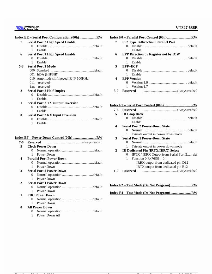
VT82C686B
Revision 1.71 June 9, 2000 -46- Register Descriptions - Super-I/O I/O Ports
7HFKQRORJLHV ,QF'HOLYHULQJ 9DOXH'HOLYHULQJ 9DOXH
Index EE – Serial Port Configuration (00h) ................... RW7 Serial Port 2 High Speed Enable
0 Disable ...................................................default1 Enable
6 Serial Port 1 High Speed Enable0 Disable ...................................................default1 Enable
5-3 Serial Port 2 Mode000 Standard ................................................default001 IrDA (HIPSIR)010 Amplitude shift keyed IR @ 500KHz011 -reserved-1xx -reserved-
2 Serial Port 2 Half Duplex0 Disable ...................................................default1 Enable
1 Serial Port 2 TX Output Inversion0 Disable ...................................................default1 Enable
0 Serial Port 2 RX Input Inversion0 Disable ...................................................default1 Enable
Index EF – Power Down Control (00h) ........................... RW7-6 Reserved ........................................ always reads 05 Clock Power Down
0 Normal operation ...................................default1 Power Down
4 Parallel Port Power Down0 Normal operation ...................................default1 Power Down
3 Serial Port 2 Power Down0 Normal operation ...................................default1 Power Down
2 Serial Port 1 Power Down0 Normal operation ...................................default1 Power Down
1 FDC Power Down0 Normal operation ...................................default1 Power Down
0 All Power Down0 Normal operation ...................................default1 Power Down All
Index F0 – Parallel Port Control (00h) ........................... RW7 PS2 Type BiDirectionl Parallel Port
0 Disable................................................... default1 Enable
6 EPP Direction by Register not by IOW0 Disable................................................... default1 Enable
5 EPP+ECP0 Disable................................................... default1 Enable
4 EPP Version0 Version 1.9 ............................................ default1 Version 1.7
3-0 Reserved ........................................always reads 0
Index F1 – Serial Port Control (00h) .............................. RW7-6 Reserved ........................................always reads 05 IR Loop Back
0 Disable................................................... default1 Enable
4 Serial Port 2 Power-Down State0 Normal................................................... default1 Tristate output in power down mode
3 Serial Port 1 Power-Down State0 Normal................................................... default1 Tristate output in power down mode
2 IR Dedicated Pin (IRTX/IRRX) Select0 IRTX / IRRX Output from Serial Port 2...... def1 Function 0 Rx76[5] = 0:
IRRX output from dedicated pin D12IRTX output from dedicated pin E12
1-0 Reserved ........................................always reads 0
Index F2 – Test Mode (Do Not Program) ....................... RW
Index F4 – Test Mode (Do Not Program) ....................... RW
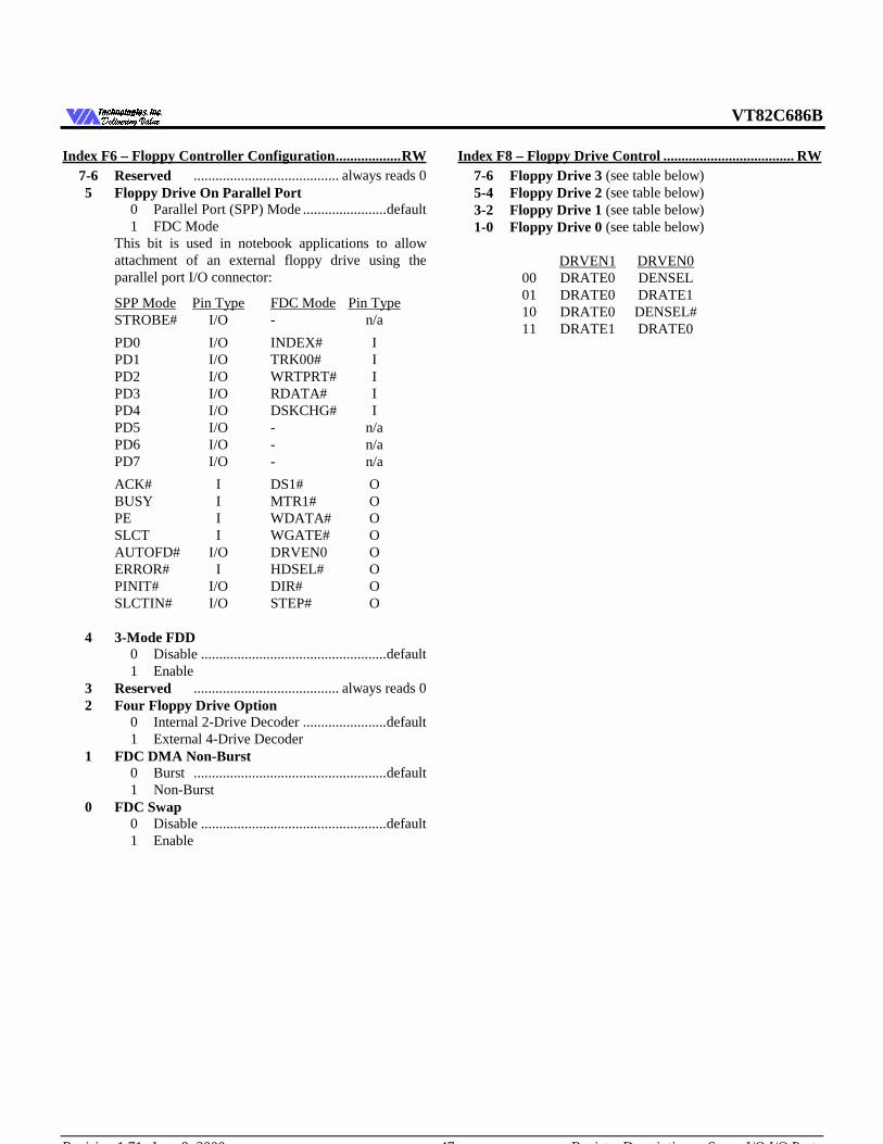
VT82C686B
Revision 1.71 June 9, 2000 -47- Register Descriptions - Super-I/O I/O Ports
7HFKQRORJLHV ,QF'HOLYHULQJ 9DOXH'HOLYHULQJ 9DOXH
Index F6 – Floppy Controller Configuration .................. RW7-6 Reserved ........................................ always reads 05 Floppy Drive On Parallel Port
0 Parallel Port (SPP) Mode .......................default1 FDC Mode
This bit is used in notebook applications to allowattachment of an external floppy drive using theparallel port I/O connector:
SPP Mode Pin Type FDC Mode Pin TypeSTROBE# I/O - n/a
PD0 I/O INDEX# IPD1 I/O TRK00# IPD2 I/O WRTPRT# IPD3 I/O RDATA# IPD4 I/O DSKCHG# IPD5 I/O - n/aPD6 I/O - n/aPD7 I/O - n/a
ACK# I DS1# OBUSY I MTR1# OPE I WDATA# OSLCT I WGATE# OAUTOFD# I/O DRVEN0 OERROR# I HDSEL# OPINIT# I/O DIR# OSLCTIN# I/O STEP# O
4 3-Mode FDD0 Disable ...................................................default1 Enable
3 Reserved ........................................ always reads 02 Four Floppy Drive Option
0 Internal 2-Drive Decoder .......................default1 External 4-Drive Decoder
1 FDC DMA Non-Burst0 Burst .....................................................default1 Non-Burst
0 FDC Swap0 Disable ...................................................default1 Enable
Index F8 – Floppy Drive Control .................................... RW7-6 Floppy Drive 3 (see table below)5-4 Floppy Drive 2 (see table below)3-2 Floppy Drive 1 (see table below)1-0 Floppy Drive 0 (see table below)
DRVEN1 DRVEN000 DRATE0 DENSEL01 DRATE0 DRATE110 DRATE0 DENSEL#11 DRATE1 DRATE0
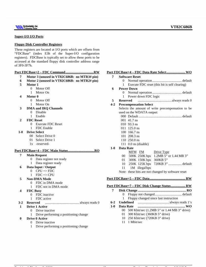
VT82C686B
Revision 1.71 June 9, 2000 -48- Register Descriptions - Super-I/O I/O Ports
7HFKQRORJLHV ,QF'HOLYHULQJ 9DOXH'HOLYHULQJ 9DOXH
Super-I/O I/O Ports
Floppy Disk Controller Registers
These registers are located at I/O ports which are offsets from“FDCBase” (index E3h of the Super-I/O configurationregisters). FDCBase is typically set to allow these ports to beaccessed at the standard floppy disk controller address rangeof 3F0-3F7h.
Port FDCBase+2 – FDC Command ................................. RW7 Motor 3 (unused in VT82C686B: no MTR3# pin)6 Motor 2 (unused in VT82C686B: no MTR2# pin)5 Motor 1
0 Motor Off1 Motor On
4 Motor 00 Motor Off1 Motor On
3 DMA and IRQ Channels0 Disable1 Enable
2 FDC Reset0 Execute FDC Reset1 FDC Enable
1-0 Drive Select00 Select Drive 001 Select Drive 11x -reserved-
Port FDCBase+4 – FDC Main Status ............................... RO7 Main Request
0 Data register not ready1 Data register ready
6 Data Input / Output0 CPU => FDC1 FDC => CPU
5 Non-DMA Mode0 FDC in DMA mode1 FDC not in DMA mode
4 FDC Busy0 FDC inactive1 FDC active
3-2 Reserved ........................................ always reads 01 Drive 1 Active
0 Drive inactive1 Drive performing a positioning change
0 Drive 0 Active0 Drive inactive1 Drive performing a positioning change
Port FDCBase+4 – FDC Data Rate Select ...................... WO7 Software Reset
0 Normal operation................................... default1 Execute FDC reset (this bit is self clearing)
6 Power Down0 Normal operation................................... default1 Power down FDC logic
5 Reserved ........................................always reads 04-2 Precompensation Select
Selects the amount of write precompensation to beused on the WDATA output:
000 Default ................................................... default001 41.7 ns010 93.3 ns011 125.0 ns100 166.7 ns101 208.3 ns110 250.0 ns111 0.0 ns (disable)
1-0 Data RateMFM FM Drive Type
00 500K 250K bps 1.2MB 5” or 1.44 MB 3”01 300K 150K bps 360KB 5”10 250K 125K bps 720KB 3” ................ default11 1M illegalbps
Note: these bits are not changed by software reset
Port FDCBase+5 – FDC Data .......................................... RW
Port FDCBase+7 – FDC Disk Change Status ................. RW7 Disk Change ......................................................... RO
0 Floppy not changed................................ default1 Floppy changed since last instruction
6-2 Undefined ..................................... always reads 1’s1-0 Data Rate ........................................................ WO
00 500 Kbit/sec (1.2MB 5” or 1.44 MB 3” drive)01 300 Kbit/sec (360KB 5” drive)10 250 Kbit/sec (720KB 3” drive)11 1 Mbit/sec
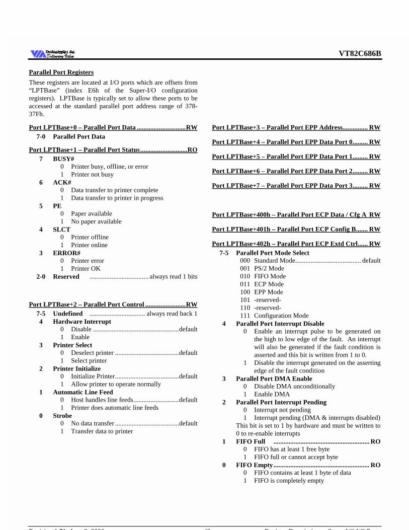
VT82C686B
Revision 1.71 June 9, 2000 -49- Register Descriptions - Super-I/O I/O Ports
7HFKQRORJLHV ,QF'HOLYHULQJ 9DOXH'HOLYHULQJ 9DOXH
Parallel Port Registers
These registers are located at I/O ports which are offsets from“LPTBase” (index E6h of the Super-I/O configurationregisters). LPTBase is typically set to allow these ports to beaccessed at the standard parallel port address range of 378-37Fh.
Port LPTBase+0 – Parallel Port Data ............................. RW7-0 Parallel Port Data
Port LPTBase+1 – Parallel Port Status ............................ RO7 BUSY#
0 Printer busy, offline, or error1 Printer not busy
6 ACK#0 Data transfer to printer complete1 Data transfer to printer in progress
5 PE0 Paper available1 No paper available
4 SLCT0 Printer offline1 Printer online
3 ERROR#0 Printer error1 Printer OK
2-0 Reserved ................................... always read 1 bits
Port LPTBase+2 – Parallel Port Control ........................ RW7-5 Undefined ................................. always read back 14 Hardware Interrupt
0 Disable ...................................................default1 Enable
3 Printer Select0 Deselect printer ......................................default1 Select printer
2 Printer Initialize0 Initialize Printer......................................default1 Allow printer to operate normally
1 Automatic Line Feed0 Host handles line feeds...........................default1 Printer does automatic line feeds
0 Strobe0 No data transfer ......................................default1 Transfer data to printer
Port LPTBase+3 – Parallel Port EPP Address............... RW
Port LPTBase+4 – Parallel Port EPP Data Port 0 ......... RW
Port LPTBase+5 – Parallel Port EPP Data Port 1 ......... RW
Port LPTBase+6 – Parallel Port EPP Data Port 2 ......... RW
Port LPTBase+7 – Parallel Port EPP Data Port 3 ......... RW
Port LPTBase+400h – Parallel Port ECP Data / Cfg A RW
Port LPTBase+401h – Parallel Port ECP Config B ....... RW
Port LPTBase+402h – Parallel Port ECP Extd Ctrl ...... RW7-5 Parallel Port Mode Select
000 Standard Mode....................................... default001 PS/2 Mode010 FIFO Mode011 ECP Mode100 EPP Mode101 -reserved-110 -reserved-111 Configuration Mode
4 Parallel Port Interrupt Disable0 Enable an interrupt pulse to be generated on
the high to low edge of the fault. An interruptwill also be generated if the fault condition isasserted and this bit is written from 1 to 0.
1 Disable the interrupt generated on the assertingedge of the fault condition
3 Parallel Port DMA Enable0 Disable DMA unconditionally1 Enable DMA
2 Parallel Port Interrupt Pending0 Interrupt not pending1 Interrupt pending (DMA & interrupts disabled)
This bit is set to 1 by hardware and must be written to0 to re-enable interrupts
1 FIFO Full ......................................................... RO0 FIFO has at least 1 free byte1 FIFO full or cannot accept byte
0 FIFO Empty......................................................... RO0 FIFO contains at least 1 byte of data1 FIFO is completely empty
VT82C686B
Revision 1.71 June 9, 2000 -50- Register Descriptions - Super-I/O I/O Ports
7HFKQRORJLHV ,QF'HOLYHULQJ 9DOXH'HOLYHULQJ 9DOXH
Serial Port 1 Registers
These registers are located at I/O ports which are offsets from“COM1Base” (index E7h of the Super-I/O configurationregisters). COM1Base is typically set to allow these ports tobe accessed at the standard serial port 1 address range of 3F8-3FFh.
Port COM1Base+0 – Transmit / Receive Buffer ............ RW7-0 Serial Data
Port COM1Base+1 – Interrupt Enable ........................... RW7-4 Undefined ..........................................always read 03 Interrupt on Handshake Input State Change2 Intr on Parity, Overrun, Framing Error or Break1 Interrupt on Transmit Buffer Empty0 Interrupt on Receive Data Ready
Port COM1Base+1-0 – Baud Rate Generator Divisor ... RW15-0 Divisor Value for Baud Rate Generator
Baud Rate = 115,200 / Divisor(e.g., setting this register to 1 selects 115.2 Kbaud)
Port COM1Base+2 – Interrupt Status ............................. RO7-3 Undefined ..........................................always read 02-1 Interrupt ID (0=highest priority)
00 Priority 3 (Handshake Input Changed State)01 Priority 2 (Transmit Buffer Empty)10 Priority 1 (Data Received)11 Priority 0 (Serialization Error or Break)
0 Interrupt Pending0 Interrupt Pending1 No Interrupt Pending
Port COM1Base+2 – FIFO Control ............................... WO
Port COM1Base+3 – UART Control ............................... RW7 Divisor Latch Access
0 Access xmit / rcv & int enable regs at 0-11 Access baud rate generator divisor latch at 0-1
6 Break0 Break condition off1 Break condition on
5-3 Parity000 None001 Odd011 Even101 Mark111 Space
2 Stop Bits0 11 2
1-0 Data Bits00 501 610 711 8
Port COM1Base+4 – Handshake Control ...................... RW7-5 Undefined ......................................... always read 04 Loopback Check
0 Normal operation1 Loopback enable
3 General Purpose Output 2 (unused in 82C686B)2 General Purpose Output 1 (unused in 82C686B)1 Request To Send
0 Disable1 Enable
0 Data Terminal Ready0 Disable1 Enable
Port COM1Base+5 – UART Status ................................. RW7 Undefined ......................................... always read 06 Transmitter Empty
0 1 byte in transmit hold or transmit shift register1 0 bytes transmit hold and transmit shift regs
5 Transmit Buffer Empty0 1 byte in transmit hold register1 Transmit hold register empty
4 Break Detected0 No break detected1 Break detected
3 Framing Error Detected0 No error1 Error
2 Parity Error Detected0 No error1 Error
1 Overrun Error Detected0 No error1 Error
0 Received Data Ready0 No received data available1 Received data in receiver buffer register
Port COM1Base+6 – Handshake Status ......................... RW7 DCD Status (1=Active, 0=Inactive)6 RI Status (1=Active, 0=Inactive)5 DSR Status (1=Active, 0=Inactive)4 CTS Status (1=Active, 0=Inactive)3 DCD Changed (1=Changed Since Last Read)2 RI Changed (1=Changed Since Last Read)1 DSR Changed (1=Changed Since Last Read)0 CTS Changed (1=Changed Since Last Read)
Port COM1Base+7 – Scratchpad .................................... RW7 Scratchpad Data

VT82C686B
Revision 1.71 June 9, 2000 -51- Register Descriptions - Super-I/O I/O Ports
7HFKQRORJLHV ,QF'HOLYHULQJ 9DOXH'HOLYHULQJ 9DOXH
Serial Port 2 Registers
These registers are located at I/O ports which are offsets from“COM2Base” (index E8h of the Super-I/O configurationregisters). COM2Base is typically set to allow these ports tobe accessed at the standard serial port 2 address range of 2F8-2FFh.
Port COM2Base+0 – Transmit / Receive Buffer ............ RW7-0 Serial Data
Port COM2Base+1 – Interrupt Enable ........................... RW7-4 Undefined ..........................................always read 03 Interrupt on Handshake Input State Change2 Intr on Parity, Overrun, Framing Error or Break1 Interrupt on Transmit Buffer Empty0 Interrupt on Receive Data Ready
Port COM2Base+1-0 – Baud Rate Generator Divisor ... RW15-0 Divisor Value for Baud Rate Generator
Baud Rate = 115,200 / Divisor(e.g., setting this register to 1 selects 115.2 Kbaud)
Port COM2Base+2 – Interrupt Status ............................. RO7-3 Undefined ..........................................always read 02-1 Interrupt ID (0=highest priority)
00 Priority 3 (Handshake Input Changed State)01 Priority 2 (Transmit Buffer Empty)10 Priority 1 (Data Received)11 Priority 0 (Serialization Error or Break)
0 Interrupt Pending0 Interrupt Pending1 No Interrupt Pending
Port COM2Base+2 – FIFO Control ............................... WO
Port COM2Base+3 – UART Control ............................... RW7 Divisor Latch Access
0 Access xmit / rcv & int enable regs at 0-11 Access baud rate generator divisor latch at 0-1
6 Break0 Break condition off1 Break condition on
5-3 Parity000 None001 Odd011 Even101 Mark111 Space
2 Stop Bits0 11 2
1-0 Data Bits00 501 610 711 8
Port COM2Base+4 – Handshake Control ...................... RW7-5 Undefined ......................................... always read 04 Loopback Check
0 Normal operation1 Loopback enable
3 General Purpose Output 2 (unused in 82C686B)2 General Purpose Output 1 (unused in 82C686B)1 Request To Send
0 Disable1 Enable
0 Data Terminal Ready0 Disable1 Enable
Port COM2Base+5 – UART Status ................................. RW7 Undefined ......................................... always read 06 Transmitter Empty
0 1 byte in transmit hold or transmit shift register1 0 bytes transmit hold and transmit shift regs
5 Transmit Buffer Empty0 1 byte in transmit hold register1 Transmit hold register empty
4 Break Detected0 No break detected1 Break detected
3 Framing Error Detected0 No error1 Error
2 Parity Error Detected0 No error1 Error
1 Overrun Error Detected0 No error1 Error
0 Received Data Ready0 No received data available1 Received data in receiver buffer register
Port COM2Base+6 – Handshake Status ......................... RW7 DCD Status (1=Active, 0=Inactive)6 RI Status (1=Active, 0=Inactive)5 DSR Status (1=Active, 0=Inactive)4 CTS Status (1=Active, 0=Inactive)3 DCD Changed (1=Changed Since Last Read)2 RI Changed (1=Changed Since Last Read)1 DSR Changed (1=Changed Since Last Read)0 CTS Changed (1=Changed Since Last Read)
Port COM2Base+7 – Scratchpad .................................... RW7 Scratchpad Data

VT82C686B
Revision 1.71 June 9, 2000 -52- Register Descriptions - Super-I/O I/O Ports
7HFKQRORJLHV ,QF'HOLYHULQJ 9DOXH'HOLYHULQJ 9DOXH
SoundBlaster Pro Port Registers
These registers are located at offsets from “SBPBase” (definedin Rx43 of Audio Function 5 PCI configuration space).SBPBase is typically set to allow these ports to be accessed atthe standard SoundBlaster Pro port address of 220h or 240h.
FM Registers
Port SBPBase+0 – FM Left Channel Index / Status ....... RW7-0 FM Right Channel Index / Status
Port SBPBase+1 – FM Left Channel Data ..................... WO7-0 Right Channel FM Data
Port SBPBase+2 – FM Right Channel Index / Status .... RW7-0 FM Right Channel Index / Status
Port SBPBase+3 – FM Right Channel Data .................. WO7-0 Right Channel FM Data
Port 388h or SBPBase+8 – FM Index / Status ................ RW7-0 FM Index / Status (Both Channels)
Writing to this port programs both the left and right channels(the write programms port offsets 0 and 2 as well)
Port 389h or SBPBase+9 – FM Data .............................. WO7-0 FM Data (Both Channels)
Writing to this port programs both the left and right channels(the write programms port offsets 1 and 3 as well)
Mixer Registers
Port SBPBase+4 – Mixer Index....................................... WO7-0 Mixer Index
Port SBPBase+5 – Mixer Data ......................................... RW7-0 Mixer Data
Sound Processor Registers
Port SBPBase+6 – Sound Processor Reset ..................... WO0 1 = Sound Processor Reset
Port SBPBase+A – Sound Processor Read Data ............. RO7-0 Sound Processor Read Data
Port SBPBase+C – Sound Processor Command / Data WO7-0 Sound Processor Command / Write Data
Port SBPBase+C – Sound Processor Buffer Status ......... RO7 1 = Sound Processor Command / Data Port Busy
Port SBPBase+E – Sound Processor Data Avail Status .. RO7 1 = Sound Processor Data Available
Register Summary - FM
Index Bit-7 Bit-6 Bit-5 Bit-4 Bit-3 Bit-2 Bit-1 Bit-001 Test02 Fast Counter (80 usec)03 Slow Counter (320 usec)04 IRQ MFC MSC SSSC SSFC08 CSM SEL
20-35 AM VIB EGT KSR Multi40-55 KSL Total Level (TL)60-75 Attack Rate (AR) Decay Rate (DR)80-95 Sustain Level (SL) Release Rate (RR)A0-A8 F-NumberB0-B8 Key Block F-Number
BD Int AM VIB Ryth Bass Snare Tom Cym HiHatC0-C8 Feedback FME0-F5 WSMFC=Mask Fast Counter SSFC=Start / Stop Fast CounterMSC=Mask Slow Counter SSSC=Start / Stop Slow Counter
Register Summary – Mixer
Index Bit-7 Bit-6 Bit-5 Bit-4 Bit-3 Bit-2 Bit-1 Bit-000 Data Reset02 SP Volume L SP Volume R0A Mic Vol0C Finp TFIL Select0E Fout ST22 General Volume General Volume26 FM Volume L FM Volume R28 CD Volume L CD Volume R2E Line Volume L Line Volume R
Finp = Input FilterFout = Output FilterTFIL = Input Filter TypeST = Stereo / Mono ModeSelect = Input Choices (0=Microphone, 1=CD, 3=Line)
Command Summary – Sound Processor (see next page)
VT82C686B
Revision 1.71 June 9, 2000 -53- Register Descriptions - Super-I/O I/O Ports
7HFKQRORJLHV ,QF'HOLYHULQJ 9DOXH'HOLYHULQJ 9DOXH
Command Summary – Sound Processor
# Type Command10 Play 8 bits directly14 Play 8 bits via DMA91 Play High-speed 8 bits via DMA16 Play 2-bit compressed via DMA17 Play 2-bit compressed via DMA with reference74 Play 4-bit compressed via DMA75 Play 4-bit compressed via DMA with reference76 Play 2.6-bit compressed via DMA77 Play 2.6-bit compressed via DMA with reference
20 Record Direct24 Record Via DMA99 Record High-speed 8 bits via DMA
D1 Speaker Turn on speaker connectionD3 Speaker Turn off speaker connectionD8 Speaker Get speaker setting
40 Misc Set sample rate48 Misc Set block length80 Misc Set silence blockD0 Misc Stop DMAD4 Misc Continue DMAE1 Misc Get version
30 MIDI Direct MIDI input31 MIDI MIDI input via interrupt32 MIDI Direct MIDI input with time stamp33 MIDI MIDI input via interrupt with time stamp34 MIDI Direct MIDI UART mode35 MIDI MIDI UART mode via interrupt36 MIDI Direct MIDI UART mode with time stamp37 MIDI MIDI UART mode via interrupt with time stamp38 MIDI Send MIDI code
Game Port Registers
These registers are fixed at the standard game port address of201h.
I/O Port 201h – Game Port Status ................................... RO7 Joystick B Button 2 Status6 Joystick B Button 1 Status5 Joystick A Button 2 Status4 Joystick A Button 1 Status3 Joystick B One-Shot Status for Y-Potentiometer2 Joystick B One-Shot Status for X-Potentiometer1 Joystick A One-Shot Status for Y-Potentiometer0 Joystick A One-Shot Status for X-Potentiometer
I/O Port 201h – Start One-Shot ....................................... WO7-0 (Value Written is Ignored)
VT82C686B
Revision 1.71 June 9, 2000 -54- Function 0 Registers - PCI to ISA Bridge
7HFKQRORJLHV ,QF'HOLYHULQJ 9DOXH'HOLYHULQJ 9DOXH
PCI Configuration Space I/O
PCI configuration space accesses for functions 0-6 use PCIconfiguration mechanism 1 (see PCI specification revision 2.2for more details). The ports respond only to double-wordaccesses. Byte or word accesses will be passed on unchanged.
Port CFB-CF8 - Configuration Address ......................... RW31 Configuration Space Enable
0 Disable ...................................................default1 Convert configuration data port writes to
configuration cycles on the PCI bus30-24 Reserved ........................................ always reads 023-16 PCI Bus Number
Used to choose a specific PCI bus in the system15-11 Device Number
Used to choose a specific device in the system10-8 Function Number
Used to choose a specific function if the selecteddevice supports multiple functions
7-2 Register NumberUsed to select a specific DWORD in the device’sconfiguration space
1-0 Fixed ........................................ always reads 0
Port CFF-CFC - Configuration Data .............................. RW
There are 7 “functions” implemented in the VT82C686B:
Function # Function
0 PCI to ISA Bridge
1 IDE Controller
2 USB Controller Ports 0-1
3 USB Controller Ports 2-3
4 Power Management, SMBus & HardwareMonitor
5 AC97 Audio Codec Controller
6 MC97 Modem Codec Controller
The following sections describe the registers and register bitsof these functions.
VT82C686B
Revision 1.71 June 9, 2000 -55- Function 0 Registers - PCI to ISA Bridge
7HFKQRORJLHV ,QF'HOLYHULQJ 9DOXH'HOLYHULQJ 9DOXH
Function 0 Registers - PCI to ISA Bridge
All registers are located in the function 0 PCI configurationspace of the VT82C686B. These registers are accessedthrough PCI configuration mechanism #1 via I/O addressCF8/CFC.
PCI Configuration Space Header
Offset 1-0 - Vendor ID = 1106h ......................................... RO
Offset 3-2 - Device ID = 0686h .......................................... RO
Offset 5-4 - Command ....................................................... RW15-8 Reserved ........................................ always reads 0
7 Address / Data Stepping0 Disable1 Enable ....................................................default
6-4 Reserved ........................................ always reads 03 Special Cycle Enable .....Normally RW†, default = 02 Bus Master ........................................ always reads 11 Memory Space .................. Normally RO†, reads as 10 I/O Space ...................... Normally RO†, reads as 1
† If the Rx46[4] test bit is set, access to bits 0, 1, and 3 aboveis reversed: bit-3 becomes read only (reading back 1) and bits0-1 become read / write (with a default of 1).
Offset 7-6 - Status ........................................................... RWC15 Detected Parity Error ....................write one to clear14 Signalled System Error...................... always reads 013 Signalled Master Abort .................write one to clear12 Received Target Abort ..................write one to clear11 Signalled Target Abort ..................write one to clear
10-9 DEVSEL# Timing .................... fixed at 01 (medium)8 Data Parity Detected.......................... always reads 07 Fast Back-to-Back.............................. always reads 0
6-0 Reserved ........................................ always reads 0
Offset 8 - Revision ID = nn ................................................ RO7-0 Revision ID
0x VT82C6861x VT82C686A4x VT82C686B
Offset 9 - Program Interface = 00h ................................... RO
Offset A - Sub Class Code = 01h ....................................... RO
Offset B - Class Code = 06h ............................................... RO
Offset E - Header Type = 80h ............................................ RO7-0 Header Type Code .........80h (Multifunction Device)
Offset F - BIST = 00h ......................................................... RO
Offset 2F-2C - Subsystem ID ............................................. ROUse offset 70-73 to change the value returned.
ISA Bus Control
Offset 40 - ISA Bus Control ............................................. RW7 ISA Command Delay
0 Normal................................................... default1 Extra
6 Extended ISA Bus Ready0 Disable................................................... default1 Enable
5 ISA Slave Wait States0 4 Wait States.......................................... default1 5 Wait States
4 Chipset I/O Wait States0 2 Wait States.......................................... default1 4 Wait States
3 I/O Recovery Time0 Disable................................................... default1 Enable
2 Extend-ALE0 Disable................................................... default1 Enable
1 ROM Wait States0 1 Wait State ........................................... default1 0 Wait States
0 ROM Write0 Disable................................................... default1 Enable
Offset 41 - ISA Test Mode ................................................ RW7 Bus Refresh Arbitration (do not program) default=06 I/O Recovery Time
0 Normal (13 BCLKs) .............................. default1 Medium (8 BCLKs)
5 Port 92 Fast Reset0 Disable................................................... default1 Enable
4 A20G Emulation (do not program) .............default=03 Double DMA Clock
0 Disable (DMA Clock = ½ ISA Clock)... default1 Enable (DMA Clock = ISA Clock)
This function can be enabled for external ISA devices(e.g., advanced Super-IO or FIR controllers) whichsupport 8MHz DMA channels. However, if this bit isset to 1, then all DMA channels will be 8 MHz. Ifthis bit is set to 1 and Rx45[n] is set to 1, then ISADMA channel ‘n’ will be 16 MHz. Therefore,typically this bit is set to 0 and the appropriate bits ofRx45 should be set to 1 to enable 8 MHz DMA clockonly for specific channels that support the higher rate.
2 SHOLD Lock During INTA (do not program) def=01 Refresh Request Test Mode (do not program).def=00 ISA Refresh
0 Disable................................................... default1 Enable
This bit should be set to 1 for ISA compatibility.

VT82C686B
Revision 1.71 June 9, 2000 -56- Function 0 Registers - PCI to ISA Bridge
7HFKQRORJLHV ,QF'HOLYHULQJ 9DOXH'HOLYHULQJ 9DOXH
Offset 42 - ISA Clock Control. ......................................... RW7 Latch IO16#
0 Enable (recommended setting) ...............default1 Disable
6 MCS16# Output0 Disable ...................................................default1 Enable
5 Master Request Test Mode (do not program)0 Disable ...................................................default1 Enable
4 Reserved (Do Not Program) ................... default = 03 ISA Clock (BCLK) Select Enable
0 BCLK = PCICLK / 4..............................default1 BCLK selected per bits 2-0
2-0 ISA Bus Clock Select (if bit-3 = 1)000 BCLK = PCICLK / 3..............................default001 BCLK = PCICLK / 2010 BCLK = PCICLK / 4011 BCLK = PCICLK / 6100 BCLK = PCICLK / 5101 BCLK = PCICLK / 10110 BCLK = PCICLK / 12111 BCLK = OSC / 2
Note: Procedure for ISA Clock switching:1) Set bit 3 to 0; 2) Change value of bit 2-0; 3) Set bit 3 to 1
Offset 43 - ROM Decode Control .................................... RWSetting these bits enables the indicated address range to beincluded in the ROMCS# decode:
7 FFFE0000h-FFFEFFFFh ..........................default=06 FFF80000h-FFFDFFFFh...........................default=05 FFF00000h-FFF7FFFFh............................default=04 000E0000h-000EFFFFh .............................default=03 000D8000h-000DFFFFh.............................default=02 000D0000h-000D7FFFh .............................default=01 000C8000h-000CFFFFh.............................default=00 000C0000h-000C7FFFh .............................default=0
Offset 44 - Keyboard Controller Control ....................... RW7 KBC Timeout Test (do not program)........default = 0
6-4 Reserved (do not program) ........................default = 03 Mouse Lock Enable
0 Disable................................................... default1 Enable
2-1 Reserved (do not program) ........................default = 00 Reserved (no function) ..............................default = 0
Offset 45 - Type F DMA Control .................................... RW7 ISA Master / DMA to PCI Line Buffer
0 Disable................................................... default1 Enable
6 DMA type F Timing on Channel 7............default=05 DMA type F Timing on Channel 6............default=04 DMA type F Timing on Channel 5............default=03 DMA type F Timing on Channel 3............default=02 DMA type F Timing on Channel 2............default=01 DMA type F Timing on Channel 1............default=00 DMA type F Timing on Channel 0............default=0
Note: For bits 0-6 above, see also Rx41[3]
VT82C686B
Revision 1.71 June 9, 2000 -57- Function 0 Registers - PCI to ISA Bridge
7HFKQRORJLHV ,QF'HOLYHULQJ 9DOXH'HOLYHULQJ 9DOXH
Offset 46 - Miscellaneous Control 1 ................................. RW7 PCI Master Write Wait States
0 0 Wait States ..........................................default1 1 Wait State
6 Gate INTR0 Disable ...................................................default1 Enable
5 Flush Line Buffer for Int or DMA IOR Cycle0 Disable ...................................................default1 Enable
4 Config Command Reg Rx04 Access (Test Only)0 Normal: Bits 0-1=RO, Bit 3=RW..........default1 Test Mode: Bits 0-1=RW, Bit-3=RO
3 Reserved (do not program)........................ default = 02 Reserved (no function) .............................. default = 01 PCI Burst Read Interruptability
0 Allow burst reads to be interrupted by ISAmaster or DMA.......................................default
1 Don’t allow PCI burst reads to be interrupted0 Posted Memory Write Enable
0 Disable ...................................................default1 Enable
The Posted Memory Write function is automaticallyenabled when Delay Transaction (see Rx47 bit-6) isenabled, independent of the state of this bit.
Offset 47 - Miscellaneous Control 2 ................................ RW7 CPU Reset Source
0 Use CPURST as CPU Reset .................. default1 Use INIT as CPU Reset
6 PCI Delay Transaction Enable0 Disable................................................... default1 Enable
The "Posted Memory Write" function isautomatically enabled when this bit is enabled,independent of the state of Rx46 bit-0.
5 EISA 4D0/4D1 Port Enable0 Disable (ignore ports 4D0-1) ................. default1 Enable (ports 4D0-1 per EISA specification)
4 Interrupt Controller Shadow Register Enable0 Disable................................................... default1 Enable (for test purposes, enable readback of
interrupt controller internal functions on I/Oreads from ports 20-21, A0-A1, A8-A9, andC8-C9) (Contact VIA Test Engineeringdepartment)
3 Reserved (always program to 0)..............default = 0Note: Always mask this bit. This bit may read back
as either 0 or 1 but must always beprogrammed with 0.
2 Write Delay Transaction Time-Out Timer0 Disable................................................... default1 Enable
1 Read Delay Transaction Time-Out Timer0 Disable................................................... default1 Enable
0 Software PCI Reset ......write 1 to generate PCI reset
VT82C686B
Revision 1.71 June 9, 2000 -58- Function 0 Registers - PCI to ISA Bridge
7HFKQRORJLHV ,QF'HOLYHULQJ 9DOXH'HOLYHULQJ 9DOXH
Offset 48 - Miscellaneous Control 3 ................................. RW7-4 Reserved ........................................ always reads 03 Extra RTC Port 74/75 Enable
0 Disable ...................................................default1 Enable
2 Integrated USB Controller Disable0 Enable.....................................................default1 Disable
1 Integrated IDE Controller Disable0 Enable.....................................................default1 Disable
0 512K PCI Memory Decode0 Use Rx4E[15-12] to select top of PCI memory1 Use contents of Rx4E[15-12] plus 512K as top
of PCI memory .......................................default
Offset 4A - IDE Interrupt Routing .................................. RW7 Wait for PGNT Before Grant to ISA Master /
DMA0 Disable ...................................................default1 Enable
6 Bus Select for Access to I/O Devices Below 100h0 Access ports 00-FFh via XD bus............default1 Access ports 00-FFh via SD bus (applies to
external devices only; internal devices such asthe mouse controller are not effected)
5-4 Reserved (do not program) ..................... default = 03-2 IDE Second Channel IRQ Routing
00 IRQ1401 IRQ15.....................................................default10 IRQ1011 IRQ11
1-0 IDE Primary Channel IRQ Routing00 IRQ14.....................................................default01 IRQ1510 IRQ1011 IRQ11
4C - ISA DMA/Master Memory Access Control 1 ........ RW7-0 PCI Memory Hole Bottom Address
These bits correspond to HA[23:16] ............default=0
4D - ISA DMA/Master Memory Access Control 2 ........ RW7-0 PCI Memory Hole Top Address (HA[23:16])
These bits correspond to HA[23:16] ............default=0
Note: Access to the memory defined in the PCI memoryhole will not be forwarded to PCI. This function isdisabled if the top address is less than or equal to thebottom address.
4F-4E - ISA DMA/Master Memory Access Control 3 ... RW15-12 Top of PCI Memory for ISA DMA/Master accesses
0000 1M .................................................... default0001 2M
... ...1111 16M
Note: All ISA DMA / Masters that access addresses higherthan the top of PCI memory will not be directed to thePCI bus.
11 Forward E0000-EFFFF Accesses to PCI........def=010 Forward A0000-BFFFF Accesses to PCI .......def=09 Forward 80000-9FFFF Accesses to PCI ........def=18 Forward 00000-7FFFF Accesses to PCI ........def=17 Forward DC000-DFFFF Accesses to PCI ......def=06 Forward D8000-DBFFF Accesses to PCI ......def=05 Forward D4000-D7FFF Accesses to PCI .......def=04 Forward D0000-D3FFF Accesses to PCI .......def=03 Forward CC000-CFFFF Accesses to PCI .....def=02 Forward C8000-CBFFF Accesses to PCI ......def=01 Forward C4000-C7FFF Accesses to PCI .......def=00 Forward C0000-C3FFF Accesses to PCI .......def=0
VT82C686B
Revision 1.71 June 9, 2000 -59- Function 0 Registers - PCI to ISA Bridge
7HFKQRORJLHV ,QF'HOLYHULQJ 9DOXH'HOLYHULQJ 9DOXH
Plug and Play Control
Offset 50 – PNP DMA Request Control .......................... RW7-4 Reserved .............................................. default = 03-2 PnP Routing for Parallel Port DRQ .....def = DRQ31-0 PnP Routing for Floppy DRQ...............def = DRQ2
DRQ Mapping: 00=DRQ0, 01=DRQ1, 10=DRQ2, 11=DRQ3
Offset 51 - PNP IRQ Routing 1 ........................................ RW7-4 PnP Routing for Parallel Port IRQ (see PnP IRQ
routing table)3-0 PnP Routing for Floppy IRQ (see PnP IRQ routing
table)
Offset 52 - PNP IRQ Routing 2 ........................................ RW7-4 PnP Routing for Serial Port 2 IRQ (see PnP IRQ
routing table)3-0 PnP Routing for Serial Port 1 IRQ (see PnP IRQ
routing table)
Offset 54 - PCI IRQ Edge / Level Select .......................... RW7-4 Reserved ........................................ always reads 0
The following bits all default to “level” triggered (0)3 PIRQA# Invert (edge) / Non-invert (level).......(1/0)2 PIRQB# Invert (edge) / Non-invert (level).......(1/0)1 PIRQC# Invert (edge) / Non-invert (level).......(1/0)0 PIRQD# Invert (edge) / Non-invert (level).......(1/0)
Note: PIRQA-D# normally connect to PCI interrupt pinsINTA-D# (see pin definitions for more information).
Offset 55 - PNP IRQ Routing 4 ........................................ RW7-4 PIRQA# Routing (see PnP IRQ routing table)3-0 Reserved ........................................ always reads 0
Offset 56 - PNP IRQ Routing 5 ........................................ RW7-4 PIRQC# Routing (see PnP IRQ routing table)3-0 PIRQB# Routing (see PnP IRQ routing table)
Offset 57 - PNP IRQ Routing 6 ........................................ RW7-4 PIRQD# Routing (see PnP IRQ routing table)3-0 Reserved ........................................ always reads 0
PnP IRQ Routing Table0000 Disable ...................................................default0001 IRQ10010 Reserved0011 IRQ30100 IRQ40101 IRQ50110 IRQ60111 IRQ71000 Reserved1001 IRQ91010 IRQ101011 IRQ111100 IRQ121101 Reserved1110 IRQ141111 IRQ15
Offset 58 – External APIC IRQ Output Control ........... RW7-5 Reserved ........................................always reads 04 ACPI IRQ to APIC[23:16] with Rx42[2:0]
0 Disable................................................... default1 Enable
3 MC97 IRQ to APIC[23:16] with Rx3C[2:0]0 Disable................................................... default1 Enable
2 AC97 IRQ to APIC[23:16] with Rx3C[2:0]0 Disable................................................... default1 Enable
1 USB Port 1 IRQ to APIC[23:16] with Rx3C[2:0]0 Disable................................................... default1 Enable
0 USB Port 0 IRQ to APIC[23:16] with Rx3C[2:0]0 Disable................................................... default1 Enable
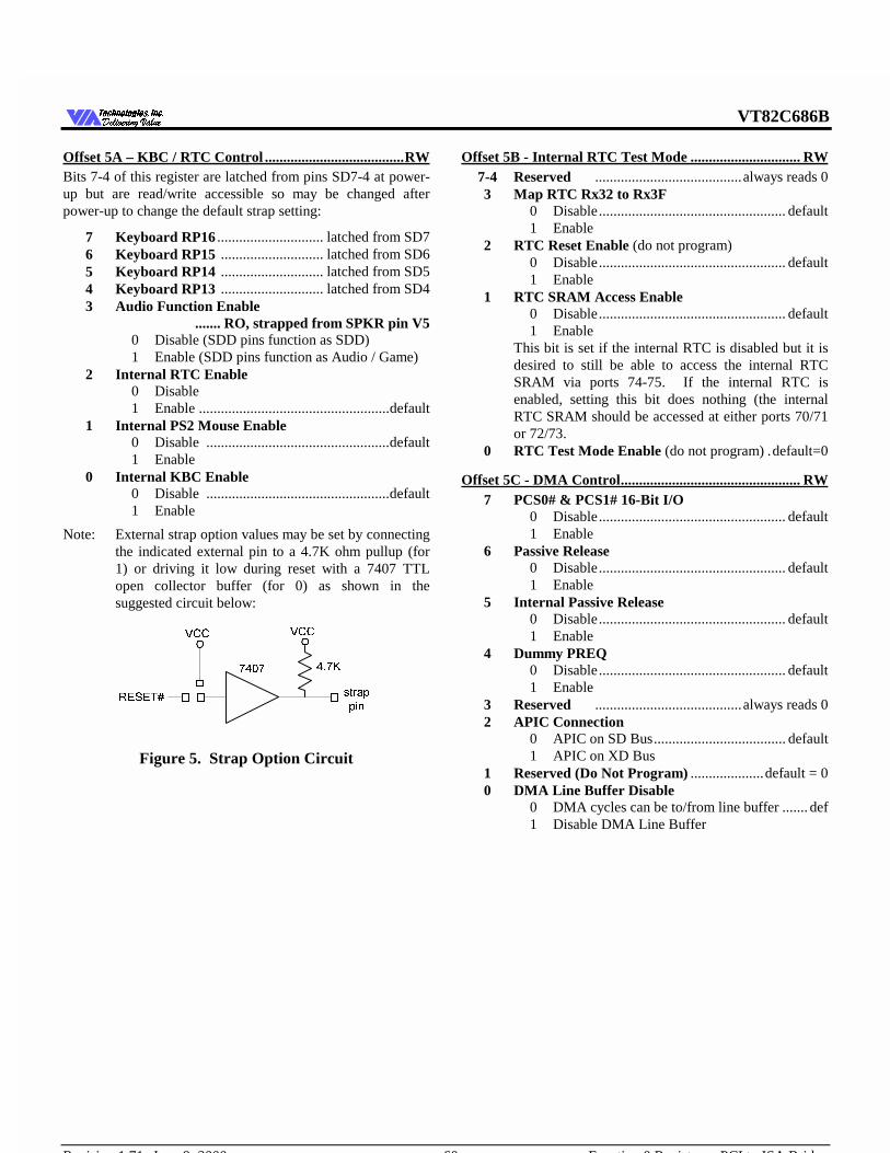
VT82C686B
Revision 1.71 June 9, 2000 -60- Function 0 Registers - PCI to ISA Bridge
7HFKQRORJLHV ,QF'HOLYHULQJ 9DOXH'HOLYHULQJ 9DOXH
Offset 5A – KBC / RTC Control ...................................... RWBits 7-4 of this register are latched from pins SD7-4 at power-up but are read/write accessible so may be changed afterpower-up to change the default strap setting:
7 Keyboard RP16 ............................. latched from SD76 Keyboard RP15 ............................ latched from SD65 Keyboard RP14 ............................ latched from SD54 Keyboard RP13 ............................ latched from SD43 Audio Function Enable
....... RO, strapped from SPKR pin V50 Disable (SDD pins function as SDD)1 Enable (SDD pins function as Audio / Game)
2 Internal RTC Enable0 Disable1 Enable ....................................................default
1 Internal PS2 Mouse Enable0 Disable ..................................................default1 Enable
0 Internal KBC Enable0 Disable ..................................................default1 Enable
Note: External strap option values may be set by connectingthe indicated external pin to a 4.7K ohm pullup (for1) or driving it low during reset with a 7407 TTLopen collector buffer (for 0) as shown in thesuggested circuit below:
9&&
.
VWUDS
SLQ5(6(7
9&&
Figure 5. Strap Option Circuit
Offset 5B - Internal RTC Test Mode .............................. RW7-4 Reserved ........................................always reads 03 Map RTC Rx32 to Rx3F
0 Disable................................................... default1 Enable
2 RTC Reset Enable (do not program)0 Disable................................................... default1 Enable
1 RTC SRAM Access Enable0 Disable................................................... default1 Enable
This bit is set if the internal RTC is disabled but it isdesired to still be able to access the internal RTCSRAM via ports 74-75. If the internal RTC isenabled, setting this bit does nothing (the internalRTC SRAM should be accessed at either ports 70/71or 72/73.
0 RTC Test Mode Enable (do not program) .default=0
Offset 5C - DMA Control ................................................. RW7 PCS0# & PCS1# 16-Bit I/O
0 Disable................................................... default1 Enable
6 Passive Release0 Disable................................................... default1 Enable
5 Internal Passive Release0 Disable................................................... default1 Enable
4 Dummy PREQ0 Disable................................................... default1 Enable
3 Reserved ........................................always reads 02 APIC Connection
0 APIC on SD Bus.................................... default1 APIC on XD Bus
1 Reserved (Do Not Program) ....................default = 00 DMA Line Buffer Disable
0 DMA cycles can be to/from line buffer ....... def1 Disable DMA Line Buffer
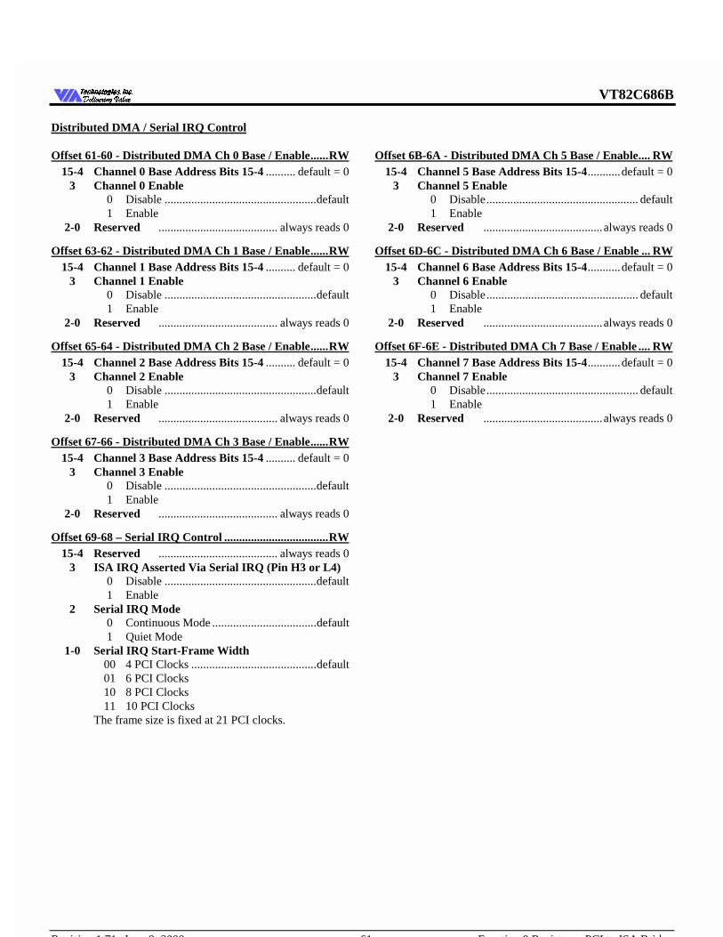
VT82C686B
Revision 1.71 June 9, 2000 -61- Function 0 Registers - PCI to ISA Bridge
7HFKQRORJLHV ,QF'HOLYHULQJ 9DOXH'HOLYHULQJ 9DOXH
Distributed DMA / Serial IRQ Control
Offset 61-60 - Distributed DMA Ch 0 Base / Enable ...... RW15-4 Channel 0 Base Address Bits 15-4 .......... default = 0
3 Channel 0 Enable0 Disable ...................................................default1 Enable
2-0 Reserved ........................................ always reads 0
Offset 63-62 - Distributed DMA Ch 1 Base / Enable ...... RW15-4 Channel 1 Base Address Bits 15-4 .......... default = 0
3 Channel 1 Enable0 Disable ...................................................default1 Enable
2-0 Reserved ........................................ always reads 0
Offset 65-64 - Distributed DMA Ch 2 Base / Enable ...... RW15-4 Channel 2 Base Address Bits 15-4 .......... default = 0
3 Channel 2 Enable0 Disable ...................................................default1 Enable
2-0 Reserved ........................................ always reads 0
Offset 67-66 - Distributed DMA Ch 3 Base / Enable ...... RW15-4 Channel 3 Base Address Bits 15-4 .......... default = 0
3 Channel 3 Enable0 Disable ...................................................default1 Enable
2-0 Reserved ........................................ always reads 0
Offset 69-68 – Serial IRQ Control ................................... RW15-4 Reserved ........................................ always reads 0
3 ISA IRQ Asserted Via Serial IRQ (Pin H3 or L4)0 Disable ...................................................default1 Enable
2 Serial IRQ Mode0 Continuous Mode ...................................default1 Quiet Mode
1-0 Serial IRQ Start-Frame Width00 4 PCI Clocks ..........................................default01 6 PCI Clocks10 8 PCI Clocks11 10 PCI Clocks
The frame size is fixed at 21 PCI clocks.
Offset 6B-6A - Distributed DMA Ch 5 Base / Enable .... RW15-4 Channel 5 Base Address Bits 15-4...........default = 0
3 Channel 5 Enable0 Disable................................................... default1 Enable
2-0 Reserved ........................................always reads 0
Offset 6D-6C - Distributed DMA Ch 6 Base / Enable ... RW15-4 Channel 6 Base Address Bits 15-4...........default = 0
3 Channel 6 Enable0 Disable................................................... default1 Enable
2-0 Reserved ........................................always reads 0
Offset 6F-6E - Distributed DMA Ch 7 Base / Enable .... RW15-4 Channel 7 Base Address Bits 15-4...........default = 0
3 Channel 7 Enable0 Disable................................................... default1 Enable
2-0 Reserved ........................................always reads 0
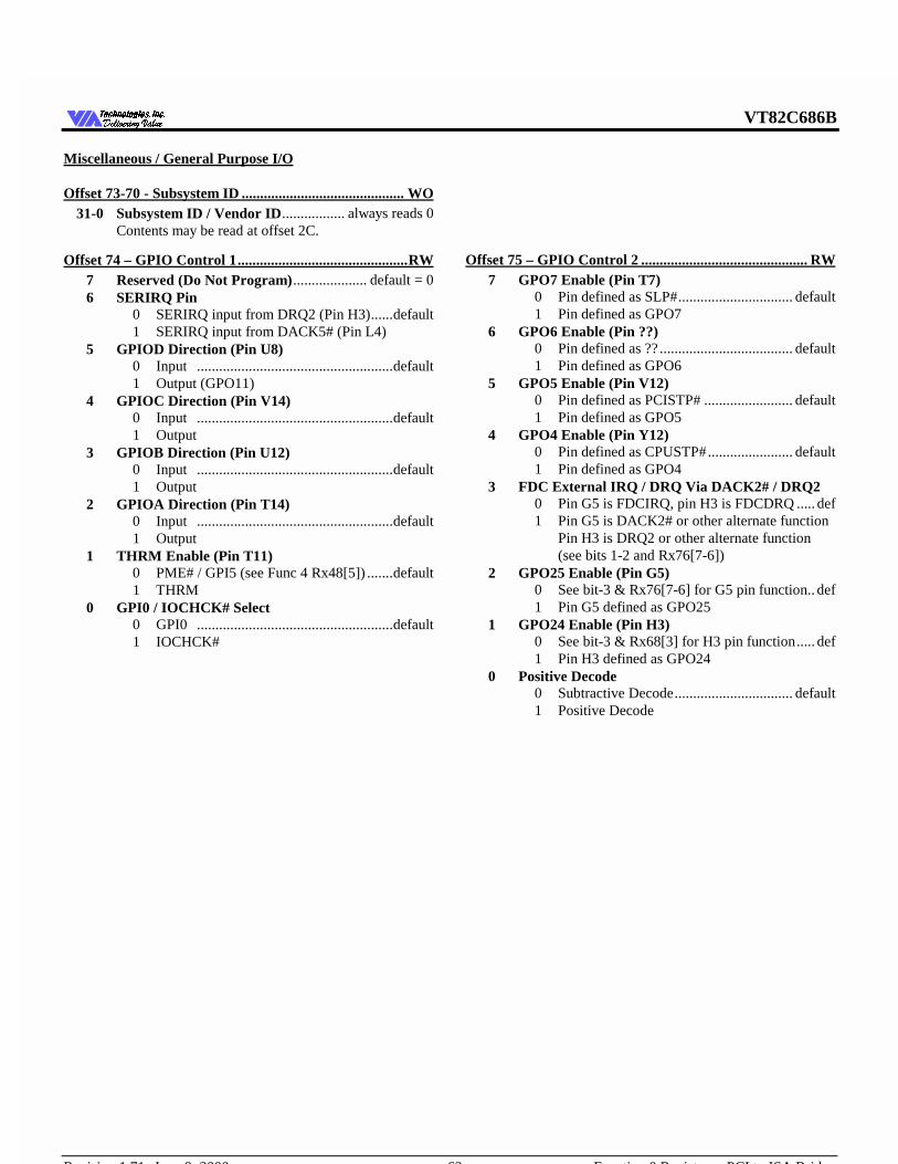
VT82C686B
Revision 1.71 June 9, 2000 -62- Function 0 Registers - PCI to ISA Bridge
7HFKQRORJLHV ,QF'HOLYHULQJ 9DOXH'HOLYHULQJ 9DOXH
Miscellaneous / General Purpose I/O
Offset 73-70 - Subsystem ID ............................................ WO31-0 Subsystem ID / Vendor ID................. always reads 0
Contents may be read at offset 2C.
Offset 74 – GPIO Control 1 .............................................. RW7 Reserved (Do Not Program).................... default = 06 SERIRQ Pin
0 SERIRQ input from DRQ2 (Pin H3)......default1 SERIRQ input from DACK5# (Pin L4)
5 GPIOD Direction (Pin U8)0 Input .....................................................default1 Output (GPO11)
4 GPIOC Direction (Pin V14)0 Input .....................................................default1 Output
3 GPIOB Direction (Pin U12)0 Input .....................................................default1 Output
2 GPIOA Direction (Pin T14)0 Input .....................................................default1 Output
1 THRM Enable (Pin T11)0 PME# / GPI5 (see Func 4 Rx48[5]) .......default1 THRM
0 GPI0 / IOCHCK# Select0 GPI0 .....................................................default1 IOCHCK#
Offset 75 – GPIO Control 2 ............................................. RW7 GPO7 Enable (Pin T7)
0 Pin defined as SLP#............................... default1 Pin defined as GPO7
6 GPO6 Enable (Pin ??)0 Pin defined as ?? .................................... default1 Pin defined as GPO6
5 GPO5 Enable (Pin V12)0 Pin defined as PCISTP# ........................ default1 Pin defined as GPO5
4 GPO4 Enable (Pin Y12)0 Pin defined as CPUSTP#....................... default1 Pin defined as GPO4
3 FDC External IRQ / DRQ Via DACK2# / DRQ20 Pin G5 is FDCIRQ, pin H3 is FDCDRQ ..... def1 Pin G5 is DACK2# or other alternate function
Pin H3 is DRQ2 or other alternate function(see bits 1-2 and Rx76[7-6])
2 GPO25 Enable (Pin G5)0 See bit-3 & Rx76[7-6] for G5 pin function.. def1 Pin G5 defined as GPO25
1 GPO24 Enable (Pin H3)0 See bit-3 & Rx68[3] for H3 pin function..... def1 Pin H3 defined as GPO24
0 Positive Decode0 Subtractive Decode................................ default1 Positive Decode
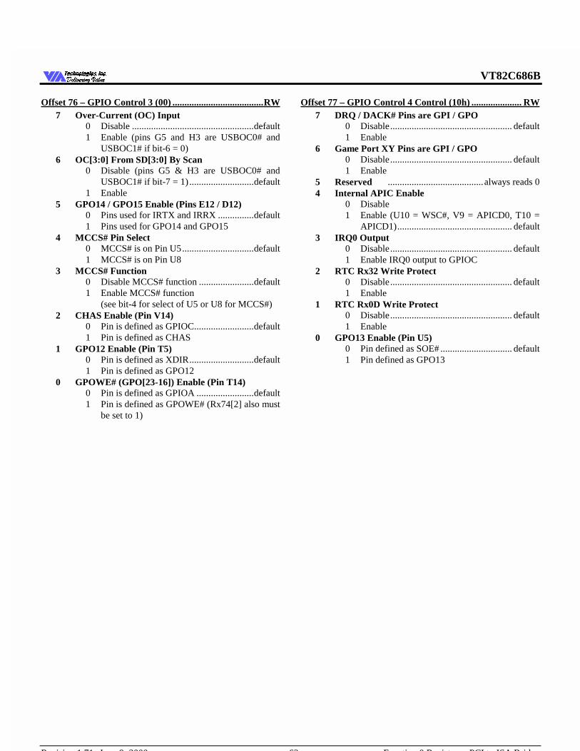
VT82C686B
Revision 1.71 June 9, 2000 -63- Function 0 Registers - PCI to ISA Bridge
7HFKQRORJLHV ,QF'HOLYHULQJ 9DOXH'HOLYHULQJ 9DOXH
Offset 76 – GPIO Control 3 (00) ...................................... RW7 Over-Current (OC) Input
0 Disable ...................................................default1 Enable (pins G5 and H3 are USBOC0# and
USBOC1# if bit-6 = 0)6 OC[3:0] From SD[3:0] By Scan
0 Disable (pins G5 & H3 are USBOC0# andUSBOC1# if bit-7 = 1) ...........................default
1 Enable5 GPO14 / GPO15 Enable (Pins E12 / D12)
0 Pins used for IRTX and IRRX ...............default1 Pins used for GPO14 and GPO15
4 MCCS# Pin Select0 MCCS# is on Pin U5..............................default1 MCCS# is on Pin U8
3 MCCS# Function0 Disable MCCS# function .......................default1 Enable MCCS# function
(see bit-4 for select of U5 or U8 for MCCS#)2 CHAS Enable (Pin V14)
0 Pin is defined as GPIOC.........................default1 Pin is defined as CHAS
1 GPO12 Enable (Pin T5)0 Pin is defined as XDIR...........................default1 Pin is defined as GPO12
0 GPOWE# (GPO[23-16]) Enable (Pin T14)0 Pin is defined as GPIOA ........................default1 Pin is defined as GPOWE# (Rx74[2] also must
be set to 1)
Offset 77 – GPIO Control 4 Control (10h) ..................... RW7 DRQ / DACK# Pins are GPI / GPO
0 Disable................................................... default1 Enable
6 Game Port XY Pins are GPI / GPO0 Disable................................................... default1 Enable
5 Reserved ........................................always reads 04 Internal APIC Enable
0 Disable1 Enable (U10 = WSC#, V9 = APICD0, T10 =
APICD1)................................................ default3 IRQ0 Output
0 Disable................................................... default1 Enable IRQ0 output to GPIOC
2 RTC Rx32 Write Protect0 Disable................................................... default1 Enable
1 RTC Rx0D Write Protect0 Disable................................................... default1 Enable
0 GPO13 Enable (Pin U5)0 Pin defined as SOE# .............................. default1 Pin defined as GPO13
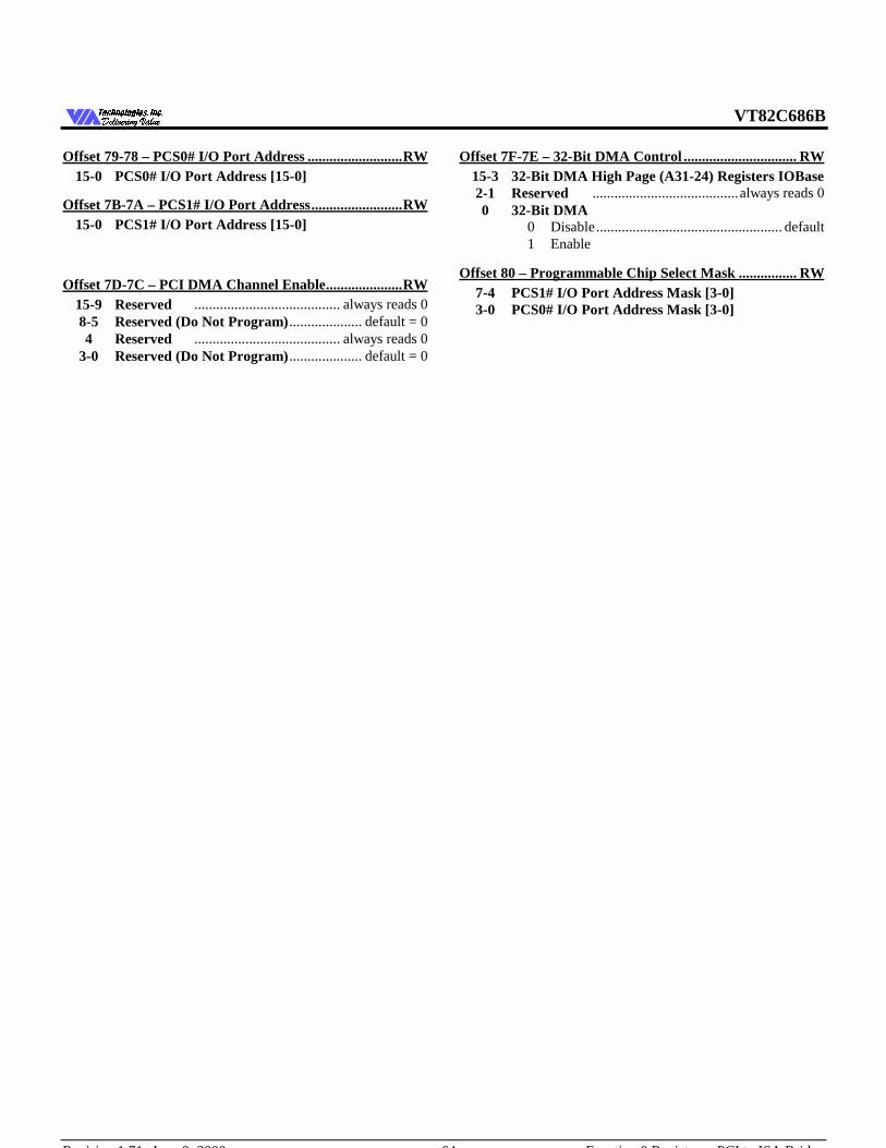
VT82C686B
Revision 1.71 June 9, 2000 -64- Function 0 Registers - PCI to ISA Bridge
7HFKQRORJLHV ,QF'HOLYHULQJ 9DOXH'HOLYHULQJ 9DOXH
Offset 79-78 – PCS0# I/O Port Address .......................... RW15-0 PCS0# I/O Port Address [15-0]
Offset 7B-7A – PCS1# I/O Port Address ......................... RW15-0 PCS1# I/O Port Address [15-0]
Offset 7D-7C – PCI DMA Channel Enable ..................... RW15-9 Reserved ........................................ always reads 08-5 Reserved (Do Not Program).................... default = 04 Reserved ........................................ always reads 0
3-0 Reserved (Do Not Program).................... default = 0
Offset 7F-7E – 32-Bit DMA Control ............................... RW15-3 32-Bit DMA High Page (A31-24) Registers IOBase2-1 Reserved ........................................always reads 00 32-Bit DMA
0 Disable................................................... default1 Enable
Offset 80 – Programmable Chip Select Mask ................ RW7-4 PCS1# I/O Port Address Mask [3-0]3-0 PCS0# I/O Port Address Mask [3-0]
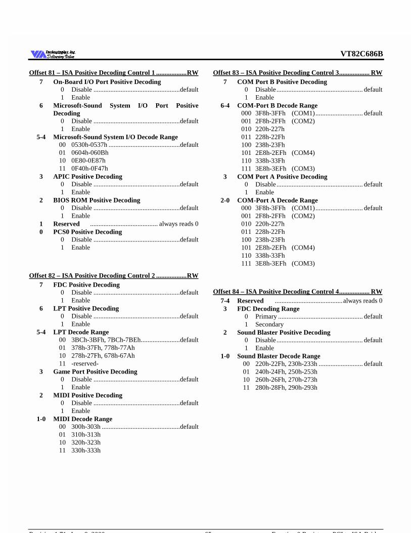
VT82C686B
Revision 1.71 June 9, 2000 -65- Function 0 Registers - PCI to ISA Bridge
7HFKQRORJLHV ,QF'HOLYHULQJ 9DOXH'HOLYHULQJ 9DOXH
Offset 81 – ISA Positive Decoding Control 1 .................. RW7 On-Board I/O Port Positive Decoding
0 Disable ...................................................default1 Enable
6 Microsoft-Sound System I/O Port PositiveDecoding
0 Disable ...................................................default1 Enable
5-4 Microsoft-Sound System I/O Decode Range00 0530h-0537h ..........................................default01 0604h-060Bh10 0E80-0E87h11 0F40h-0F47h
3 APIC Positive Decoding0 Disable ...................................................default1 Enable
2 BIOS ROM Positive Decoding0 Disable ...................................................default1 Enable
1 Reserved ........................................ always reads 00 PCS0 Positive Decoding
0 Disable ...................................................default1 Enable
Offset 82 – ISA Positive Decoding Control 2 .................. RW7 FDC Positive Decoding
0 Disable ...................................................default1 Enable
6 LPT Positive Decoding0 Disable ...................................................default1 Enable
5-4 LPT Decode Range00 3BCh-3BFh, 7BCh-7BEh.......................default01 378h-37Fh, 778h-77Ah10 278h-27Fh, 678h-67Ah11 -reserved-
3 Game Port Positive Decoding0 Disable ...................................................default1 Enable
2 MIDI Positive Decoding0 Disable ...................................................default1 Enable
1-0 MIDI Decode Range00 300h-303h ..............................................default01 310h-313h10 320h-323h11 330h-333h
Offset 83 – ISA Positive Decoding Control 3 .................. RW7 COM Port B Positive Decoding
0 Disable................................................... default1 Enable
6-4 COM-Port B Decode Range000 3F8h-3FFh (COM1)............................ default001 2F8h-2FFh (COM2)010 220h-227h011 228h-22Fh100 238h-23Fh101 2E8h-2EFh (COM4)110 338h-33Fh111 3E8h-3EFh (COM3)
3 COM Port A Positive Decoding0 Disable................................................... default1 Enable
2-0 COM-Port A Decode Range000 3F8h-3FFh (COM1)............................ default001 2F8h-2FFh (COM2)010 220h-227h011 228h-22Fh100 238h-23Fh101 2E8h-2EFh (COM4)110 338h-33Fh111 3E8h-3EFh (COM3)
Offset 84 – ISA Positive Decoding Control 4 .................. RW7-4 Reserved ........................................always reads 03 FDC Decoding Range
0 Primary .................................................. default1 Secondary
2 Sound Blaster Positive Decoding0 Disable................................................... default1 Enable
1-0 Sound Blaster Decode Range00 220h-22Fh, 230h-233h .......................... default01 240h-24Fh, 250h-253h10 260h-26Fh, 270h-273h11 280h-28Fh, 290h-293h
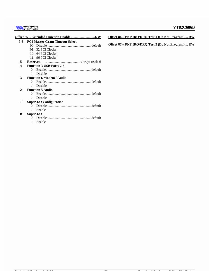
VT82C686B
Revision 1.71 June 9, 2000 -66- Function 0 Registers - PCI to ISA Bridge
7HFKQRORJLHV ,QF'HOLYHULQJ 9DOXH'HOLYHULQJ 9DOXH
Offset 85 – Extended Function Enable ............................ RW7-6 PCI Master Grant Timeout Select
00 Disable ...................................................default01 32 PCI Clocks10 64 PCI Clocks11 96 PCI Clocks
5 Reserved ........................................ always reads 04 Function 3 USB Ports 2-3
0 Enable.....................................................default1 Disable
3 Function 6 Modem / Audio0 Enable.....................................................default1 Disable
2 Function 5 Audio0 Enable.....................................................default1 Disable
1 Super-I/O Configuration0 Disable ...................................................default1 Enable
0 Super-I/O0 Disable ...................................................default1 Enable
Offset 86 – PNP IRQ/DRQ Test 1 (Do Not Program) ... RW
Offset 87 – PNP IRQ/DRQ Test 2 (Do Not Program) ... RW
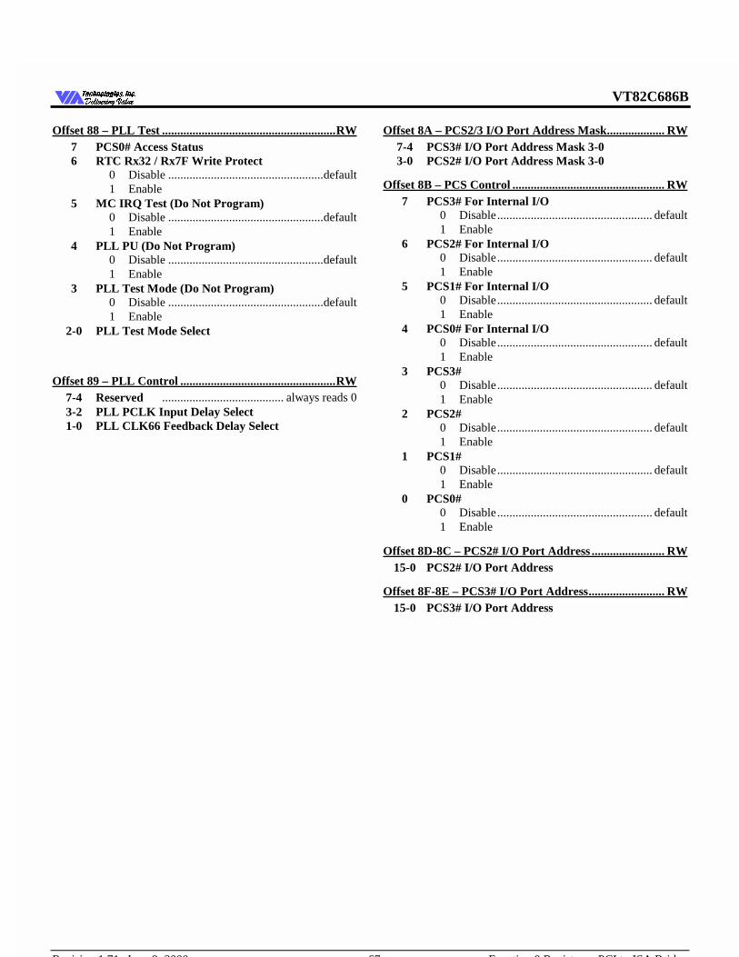
VT82C686B
Revision 1.71 June 9, 2000 -67- Function 0 Registers - PCI to ISA Bridge
7HFKQRORJLHV ,QF'HOLYHULQJ 9DOXH'HOLYHULQJ 9DOXH
Offset 88 – PLL Test ......................................................... RW7 PCS0# Access Status6 RTC Rx32 / Rx7F Write Protect
0 Disable ...................................................default1 Enable
5 MC IRQ Test (Do Not Program)0 Disable ...................................................default1 Enable
4 PLL PU (Do Not Program)0 Disable ...................................................default1 Enable
3 PLL Test Mode (Do Not Program)0 Disable ...................................................default1 Enable
2-0 PLL Test Mode Select
Offset 89 – PLL Control ................................................... RW7-4 Reserved ........................................ always reads 03-2 PLL PCLK Input Delay Select1-0 PLL CLK66 Feedback Delay Select
Offset 8A – PCS2/3 I/O Port Address Mask ................... RW7-4 PCS3# I/O Port Address Mask 3-03-0 PCS2# I/O Port Address Mask 3-0
Offset 8B – PCS Control .................................................. RW7 PCS3# For Internal I/O
0 Disable................................................... default1 Enable
6 PCS2# For Internal I/O0 Disable................................................... default1 Enable
5 PCS1# For Internal I/O0 Disable................................................... default1 Enable
4 PCS0# For Internal I/O0 Disable................................................... default1 Enable
3 PCS3#0 Disable................................................... default1 Enable
2 PCS2#0 Disable................................................... default1 Enable
1 PCS1#0 Disable................................................... default1 Enable
0 PCS0#0 Disable................................................... default1 Enable
Offset 8D-8C – PCS2# I/O Port Address ........................ RW15-0 PCS2# I/O Port Address
Offset 8F-8E – PCS3# I/O Port Address ......................... RW15-0 PCS3# I/O Port Address
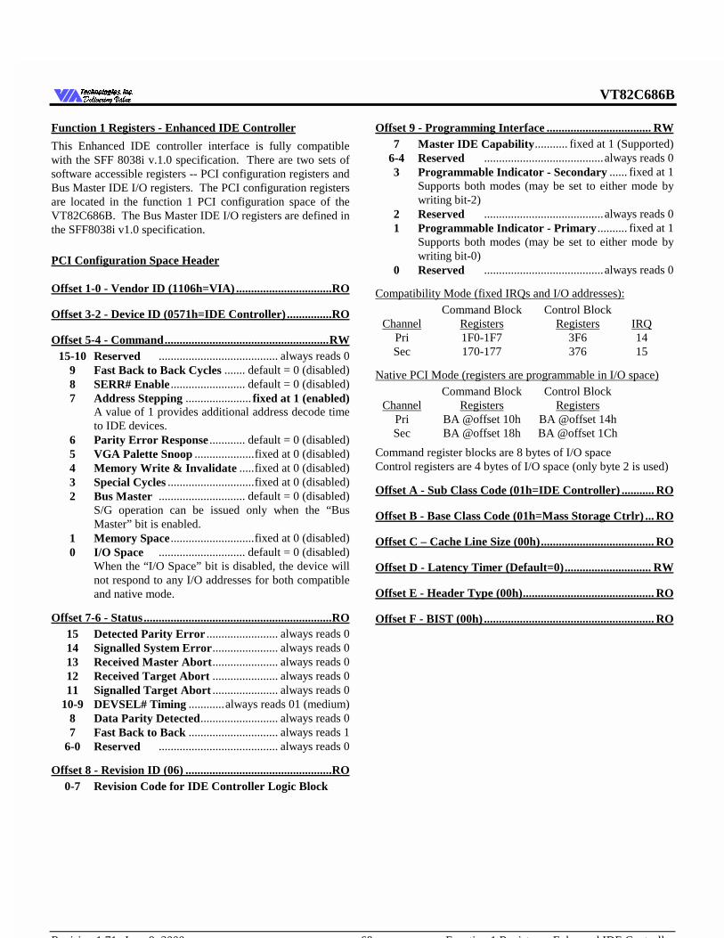
VT82C686B
Revision 1.71 June 9, 2000 -68- Function 1 Registers - Enhanced IDE Controller
7HFKQRORJLHV ,QF'HOLYHULQJ 9DOXH'HOLYHULQJ 9DOXH
Function 1 Registers - Enhanced IDE Controller
This Enhanced IDE controller interface is fully compatiblewith the SFF 8038i v.1.0 specification. There are two sets ofsoftware accessible registers -- PCI configuration registers andBus Master IDE I/O registers. The PCI configuration registersare located in the function 1 PCI configuration space of theVT82C686B. The Bus Master IDE I/O registers are defined inthe SFF8038i v1.0 specification.
PCI Configuration Space Header
Offset 1-0 - Vendor ID (1106h=VIA) ................................ RO
Offset 3-2 - Device ID (0571h=IDE Controller) ............... RO
Offset 5-4 - Command ....................................................... RW15-10 Reserved ........................................ always reads 0
9 Fast Back to Back Cycles ....... default = 0 (disabled)8 SERR# Enable ......................... default = 0 (disabled)7 Address Stepping ...................... fixed at 1 (enabled)
A value of 1 provides additional address decode timeto IDE devices.
6 Parity Error Response ............ default = 0 (disabled)5 VGA Palette Snoop ....................fixed at 0 (disabled)4 Memory Write & Invalidate .....fixed at 0 (disabled)3 Special Cycles .............................fixed at 0 (disabled)2 Bus Master ............................. default = 0 (disabled)
S/G operation can be issued only when the “BusMaster” bit is enabled.
1 Memory Space ............................fixed at 0 (disabled)0 I/O Space ............................. default = 0 (disabled)
When the “I/O Space” bit is disabled, the device willnot respond to any I/O addresses for both compatibleand native mode.
Offset 7-6 - Status ............................................................... RO15 Detected Parity Error ........................ always reads 014 Signalled System Error...................... always reads 013 Received Master Abort...................... always reads 012 Received Target Abort ...................... always reads 011 Signalled Target Abort ...................... always reads 0
10-9 DEVSEL# Timing ............always reads 01 (medium)8 Data Parity Detected.......................... always reads 07 Fast Back to Back .............................. always reads 1
6-0 Reserved ........................................ always reads 0
Offset 8 - Revision ID (06) ................................................. RO0-7 Revision Code for IDE Controller Logic Block
Offset 9 - Programming Interface ................................... RW7 Master IDE Capability........... fixed at 1 (Supported)
6-4 Reserved ........................................always reads 03 Programmable Indicator - Secondary ...... fixed at 1
Supports both modes (may be set to either mode bywriting bit-2)
2 Reserved ........................................always reads 01 Programmable Indicator - Primary .......... fixed at 1
Supports both modes (may be set to either mode bywriting bit-0)
0 Reserved ........................................always reads 0
Compatibility Mode (fixed IRQs and I/O addresses):Command Block Control Block
Channel Registers Registers IRQPri 1F0-1F7 3F6 14Sec 170-177 376 15
Native PCI Mode (registers are programmable in I/O space)Command Block Control Block
Channel Registers RegistersPri BA @offset 10h BA @offset 14hSec BA @offset 18h BA @offset 1Ch
Command register blocks are 8 bytes of I/O spaceControl registers are 4 bytes of I/O space (only byte 2 is used)
Offset A - Sub Class Code (01h=IDE Controller) ........... RO
Offset B - Base Class Code (01h=Mass Storage Ctrlr) ... RO
Offset C – Cache Line Size (00h) ...................................... RO
Offset D - Latency Timer (Default=0) ............................. RW
Offset E - Header Type (00h) ............................................ RO
Offset F - BIST (00h) ......................................................... RO
VT82C686B
Revision 1.71 June 9, 2000 -69- Function 1 Registers - Enhanced IDE Controller
7HFKQRORJLHV ,QF'HOLYHULQJ 9DOXH'HOLYHULQJ 9DOXH
Offset 13-10 - Pri Data / Command Base Address.......... RWSpecifies an 8 byte I/O address space.
31-16 Reserved ..........................................always read 015-3 Port Address ....................................... default=01F0h2-0 Fixed at 001b ..................................................... fixed
Offset 17-14 - Pri Control / Status Base Address............ RWSpecifies a 4 byte I/O address space of which only the thirdbyte is active (i.e., 3F6h for the default base address of 3F4h).
31-16 Reserved ..........................................always read 015-2 Port Address ....................................... default=03F4h1-0 Fixed at 01b ....................................................... fixed
Offset 1B-18 - Sec Data / Command Base Address ........ RWSpecifies an 8 byte I/O address space.
31-16 Reserved ..........................................always read 015-3 Port Address ...................................... default=0170h2-0 Fixed at 001b ..................................................... fixed
Offset 1F-1C - Sec Control / Status Base Address .......... RWSpecifies a 4 byte I/O address space of which only the thirdbyte is active (i.e., 376h for the default base address of 374h).
31-16 Reserved ..........................................always read 015-2 Port Address ...................................... default=0374h1-0 Fixed at 01b ....................................................... fixed
Offset 23-20 - Bus Master Control Regs Base Address .. RWSpecifies a 16 byte I/O address space compliant with the SFF-8038i rev 1.0 specification.
31-16 Reserved ..........................................always read 015-4 Port Address ....................................... default=CC0h3-0 Fixed at 0001b .................................................. fixed
Offset 34 - Capability Pointer (C0h) ................................ RO
Offset 3C - Interrupt Line (0Eh) ...................................... RO
Offset 3D - Interrupt Pin (00h) ......................................... RO7-0 Interrupt Routing Mode
00h Legacy mode interrupt routing............... default01h Native mode interrupt routing
Offset 3E - Min Gnt (00h) ................................................. RO
Offset 3F - Max Latency (00h).......................................... RO
VT82C686B
Revision 1.71 June 9, 2000 -70- Function 1 Registers - Enhanced IDE Controller
7HFKQRORJLHV ,QF'HOLYHULQJ 9DOXH'HOLYHULQJ 9DOXH
IDE-Controller-Specific Confiiguration Registers
Offset 40 - Chip Enable (00h) ........................................... RW7-4 Reserved ........................................ always reads 03-2 Reserved (Do Not Program)...........R/W, default = 01 Primary Channel Enable ........ default = 0 (disabled)0 Secondary Channel Enable .... default = 0 (disabled)
Offset 41 - IDE Configuration I (06h) ............................. RW7 Primary IDE Read Prefetch Buffer
0 Disable ...................................................default1 Enable
6 Primary IDE Post Write Buffer0 Disable ...................................................default1 Enable
5 Secondary IDE Read Prefetch Buffer0 Disable ...................................................default1 Enable
4 Secondary IDE Post Write Buffer0 Disable ...................................................default1 Enable
3-2 Reserved ........................................ always reads 01 Reserved (Do Not Program)...................... default=10 Reserved ........................................ always reads 0
Offset 42 - IDE Configuration II (09h) ............................ RW7-2 Reserved (Do Not Program)........ default = 000010b1-0 DEVSEL# Timing Select ..................... default = 01b
(also reflected in Rx07)
Offset 43 - FIFO Configuration (0Ah) ............................. RW7-4 Reserved ........................................ always reads 03-2 Threshold for Primary Channel
00 001 1/410 1/2 .....................................................default11 3/4
1-0 Threshold for Secondary Channel00 001 1/410 1/2 .....................................................default11 3/4
Offset 44 - Miscellaneous Control 1 (68h) ...................... RW7 Reserved ........................................always reads 06 Master Read Cycle IRDY# Wait States
0 0 wait states1 1 wait state ............................................. default
5 Master Write Cycle IRDY# Wait States0 0 wait states1 1 wait state ............................................. default
4 PIO Read Prefetch Byte Counter0 Disable................................................... default1 Enable
3 Bus Master IDE Status Register Read RetryRetry bus master IDE status register read whenmaster write operation for DMA read is not complete
0 Disable1 Enable .................................................... default
2 Packet Command Prefetching0 Disable................................................... default1 Enable
1 Reserved ........................................always reads 00 UltraDMA Host Must Wait for First Strobe
Before Termination0 Enable .................................................... default1 Disable
Offset 45 - Miscellaneous Control 2 (00h) ...................... RW7 Reserved ........................................always reads 06 Interrupt Steering Swap
0 Don’t swap channel interrupts ............... default1 Swap interrupts between the two channels
5 Reserved ........................................always reads 04 Rx3C Write Protect
0 Disable................................................... default1 Enable
3 Memory Read Multiple Command0 Disable................................................... default1 Enable
2 Memory Read and Invalidate Command0 Disable................................................... default1 Enable
1-0 Reserved ........................................always reads 0
Offset 46 - Miscellaneous Control 3 (C0h) ..................... RW7 Primary Channel Read DMA FIFO Flush
0 Disable1 Enable FIFO flush for Read DMA when
interrupt asserts primary channel. .......... default6 Secondary Channel Read DMA FIFO Flush
0 Disable1 Enable FIFO flush for Read DMA when
interrupt asserts secondary channel........ default5-0 Reserved ........................................always reads 0
VT82C686B
Revision 1.71 June 9, 2000 -71- Function 1 Registers - Enhanced IDE Controller
7HFKQRORJLHV ,QF'HOLYHULQJ 9DOXH'HOLYHULQJ 9DOXH
Offset 4B-48 - Drive Timing Control (A8A8A8A8h) ...... RWThe following fields define the Active Pulse Width andRecovery Time for the IDE DIOR# and DIOW# signals:
31-28 Primary Drive 0 Active Pulse Width ...... def=1010b27-24 Primary Drive 0 Recovery Time ............. def=1000b23-20 Primary Drive 1 Active Pulse Width ...... def=1010b19-16 Primary Drive 1 Recovery Time ............. def=1000b15-12 Secondary Drive 0 Active Pulse Width .. def=1010b11-8 Secondary Drive 0 Recovery Time ......... def=1000b7-4 Secondary Drive 1 Active Pulse Width .. def=1010b3-0 Secondary Drive 1 Recovery Time ......... def=1000b
The actual value for each field is the encoded value in the fieldplus one and indicates the number of PCI clocks.
Offset 4C - Address Setup Time (FFh) ............................ RW7-6 Primary Drive 0 Address Setup Time ........ def = 115-4 Primary Drive 1 Address Setup Time ....... def = 113-2 Secondary Drive 0 Address Setup Time .... def = 111-0 Secondary Drive 1 Address Setup Time .... def = 11
For each field above:00 1T01 2T10 3T11 4T .....................................................default
Offset 53-50 - UltraDMA Extended Timing Control ..... RW31 Pri Drive 0 UltraDMA-Mode Enable Method
0 Enable by using “Set Feature” command..... def1 Enable by setting bit-30 of this register
30 Pri Drive 0 UltraDMA-Mode Enable0 Disable................................................... default1 Enable UltraDMA-Mode Operation
29 Pri Drive 0 Transfer Mode0 DMA or PIO Mode ............................... default1 UltraDMA Mode
28 Pri Drive 0 Cabal Type Reporting0 Disable................................................... default1 Enable
27 Reserved ........................................always reads 026-24 Pri Drive 0 Cycle Time (T = 10nsec)
000 2T001 3T010 4T011 5T100 6T101 7T110 8T111 9T .................................................... default
23 Pri Drive 1 UltraDMA-Mode Enable Method22 Pri Drive 1 UltraDMA-Mode Enable21 Pri Drive 1 Transfer Mode20 Pri Drive 1 Cabal Type Reporting
0 Disable................................................... default1 Enable
19 Reserved ........................................always reads 018-16 Pri Drive 1 Cycle Time.......... (see above for default)
15 Sec Drive 0 UltraDMA-Mode Enable Method14 Sec Drive 0 UltraDMA-Mode Enable13 Sec Drive 0 Transfer Mode12 Sec Drive 0 Cabal Type Reporting
0 Disable................................................... default1 Enable
11 Reserved ........................................always reads 010-8 Sec Drive 0 Cycle Time ......... (see above for default)
7 Sec Drive 1 UltraDMA-Mode Enable Method6 Sec Drive 1 UltraDMA-Mode Enable5 Sec Drive 1 Transfer Mode4 Sec Drive 1 Cabal Type Reporting
0 Disable................................................... default1 Enable
3 Reserved ........................................always reads 02-0 Sec Drive 1 Cycle Time ......... (see above for default)
Each byte defines UltraDMA operation for the indicated drive.The bit definitions are the same within each byte.
VT82C686B
Revision 1.71 June 9, 2000 -72- Function 1 Registers - Enhanced IDE Controller
7HFKQRORJLHV ,QF'HOLYHULQJ 9DOXH'HOLYHULQJ 9DOXH
Offset 54 – UltraDMA FIFO Control (06h) .................... RW7-5 Reserved ........................................ always reads 04 One Frame For Each PCI Request For IDE PCI
Master Cycles0 Disable ...................................................default1 Enable
3 Reserved ........................................ always reads 02 Change Drive to Clear All FIFO & Internal States
0 Disable1 Enable.....................................................default
1 Reserved ........................................ always reads 00 Complete DMA Cycle with Transfer Size Less
Than FIFO Size0 Enable.....................................................default1 Disable
Offset 61-60 - Primary Sector Size (0200h) .................... RW15-12 Reserved ........................................always reads 011-0 Number of Bytes Per Sector ...def=200h (512 bytes)
Offset 69-68 - Secondary Sector Size (0200h) ................. RW15-12 Reserved ........................................always reads 011-0 Number of Bytes Per Sector ...def=200h (512 bytes)
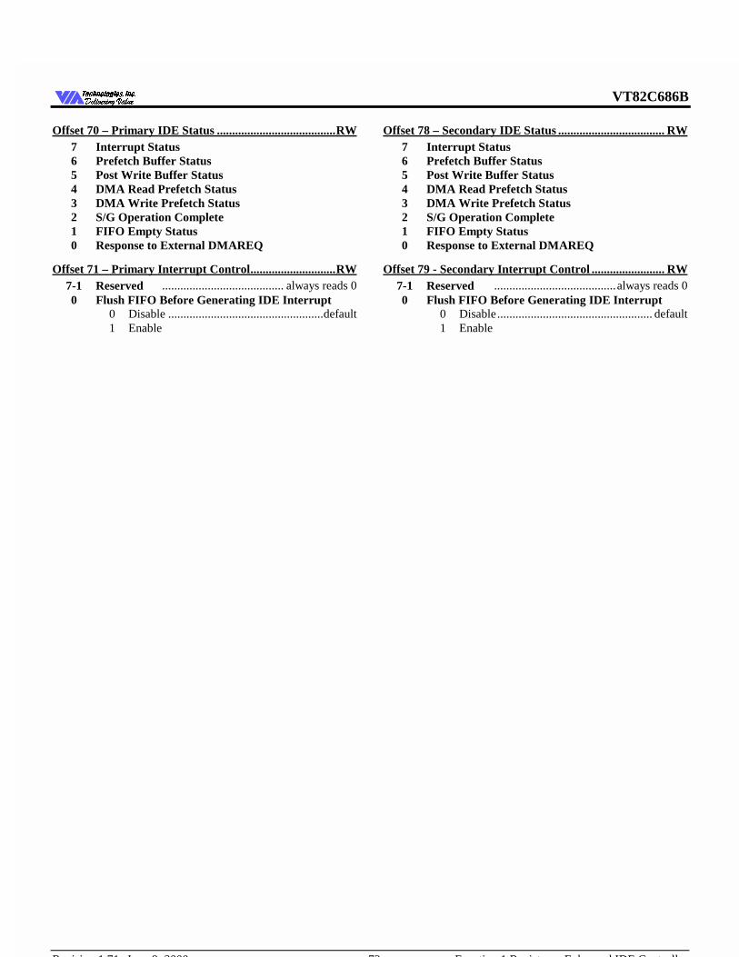
VT82C686B
Revision 1.71 June 9, 2000 -73- Function 1 Registers - Enhanced IDE Controller
7HFKQRORJLHV ,QF'HOLYHULQJ 9DOXH'HOLYHULQJ 9DOXH
Offset 70 – Primary IDE Status ....................................... RW7 Interrupt Status6 Prefetch Buffer Status5 Post Write Buffer Status4 DMA Read Prefetch Status3 DMA Write Prefetch Status2 S/G Operation Complete1 FIFO Empty Status0 Response to External DMAREQ
Offset 71 – Primary Interrupt Control ............................ RW7-1 Reserved ........................................ always reads 00 Flush FIFO Before Generating IDE Interrupt
0 Disable ...................................................default1 Enable
Offset 78 – Secondary IDE Status ................................... RW7 Interrupt Status6 Prefetch Buffer Status5 Post Write Buffer Status4 DMA Read Prefetch Status3 DMA Write Prefetch Status2 S/G Operation Complete1 FIFO Empty Status0 Response to External DMAREQ
Offset 79 - Secondary Interrupt Control ........................ RW7-1 Reserved ........................................always reads 00 Flush FIFO Before Generating IDE Interrupt
0 Disable................................................... default1 Enable
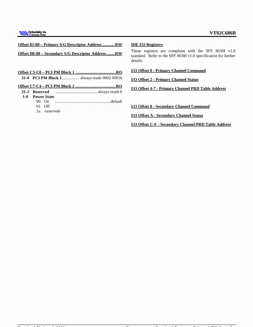
VT82C686B
Revision 1.71 June 9, 2000 -74- Function 1 Registers - Enhanced IDE Controller
7HFKQRORJLHV ,QF'HOLYHULQJ 9DOXH'HOLYHULQJ 9DOXH
Offset 83-80 – Primary S/G Descriptor Address ............ RW
Offset 8B-88 – Secondary S/G Descriptor Address ........ RW
Offset C3-C0 – PCI PM Block 1 ....................................... RO31-0 PCI PM Block 1................. always reads 0002 0001h
Offset C7-C4 – PCI PM Block 2 ....................................... RO31-2 Reserved ........................................ always reads 01-0 Power State
00 On .....................................................default01 Off1x -reserved-
IDE I/O Registers
These registers are compliant with the SFF 8038I v1.0standard. Refer to the SFF 8038I v1.0 specification for furtherdetails.
I/O Offset 0 - Primary Channel Command
I/O Offset 2 - Primary Channel Status
I/O Offset 4-7 - Primary Channel PRD Table Address
I/O Offset 8 - Secondary Channel Command
I/O Offset A - Secondary Channel Status
I/O Offset C-F - Secondary Channel PRD Table Address
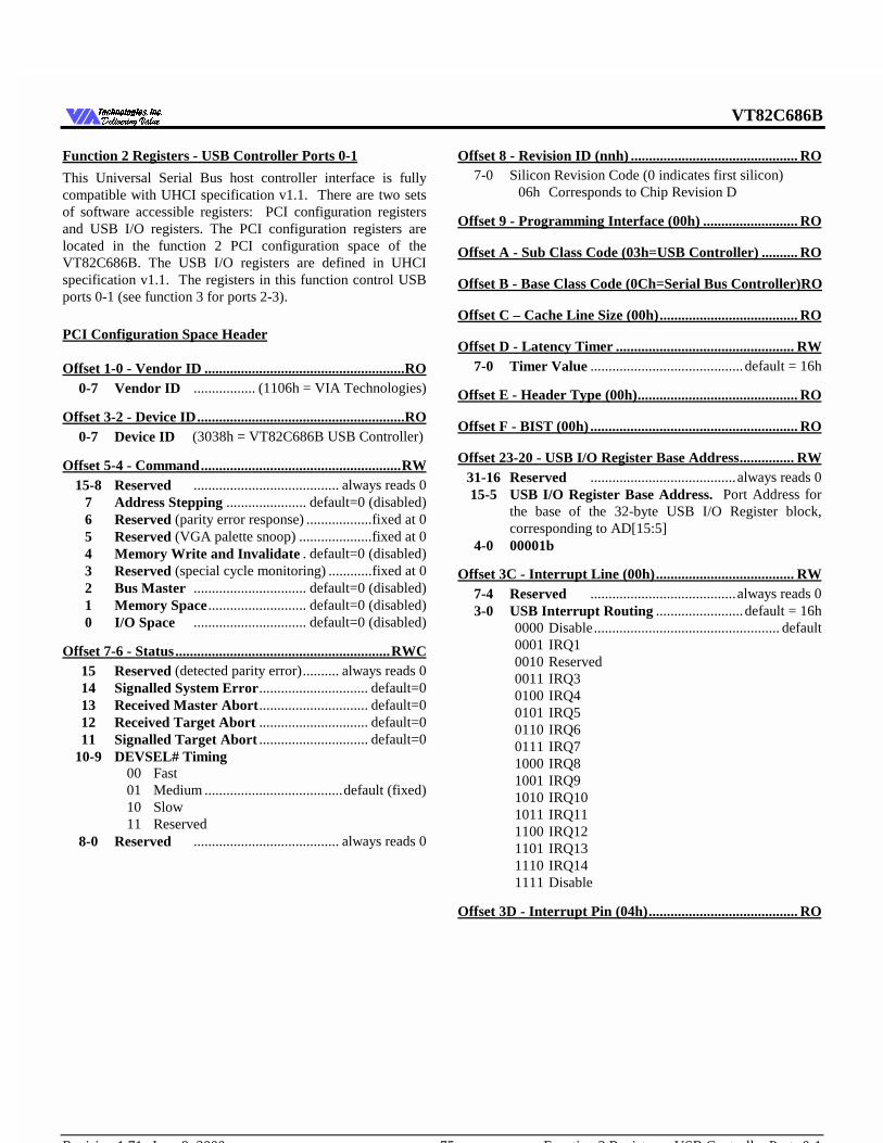
VT82C686B
Revision 1.71 June 9, 2000 -75- Function 2 Registers - USB Controller Ports 0-1
7HFKQRORJLHV ,QF'HOLYHULQJ 9DOXH'HOLYHULQJ 9DOXH
Function 2 Registers - USB Controller Ports 0-1
This Universal Serial Bus host controller interface is fullycompatible with UHCI specification v1.1. There are two setsof software accessible registers: PCI configuration registersand USB I/O registers. The PCI configuration registers arelocated in the function 2 PCI configuration space of theVT82C686B. The USB I/O registers are defined in UHCIspecification v1.1. The registers in this function control USBports 0-1 (see function 3 for ports 2-3).
PCI Configuration Space Header
Offset 1-0 - Vendor ID ....................................................... RO0-7 Vendor ID ................. (1106h = VIA Technologies)
Offset 3-2 - Device ID ......................................................... RO0-7 Device ID (3038h = VT82C686B USB Controller)
Offset 5-4 - Command ....................................................... RW15-8 Reserved ........................................ always reads 0
7 Address Stepping ...................... default=0 (disabled)6 Reserved (parity error response) ..................fixed at 05 Reserved (VGA palette snoop) ....................fixed at 04 Memory Write and Invalidate . default=0 (disabled)3 Reserved (special cycle monitoring) ............fixed at 02 Bus Master ............................... default=0 (disabled)1 Memory Space ........................... default=0 (disabled)0 I/O Space ............................... default=0 (disabled)
Offset 7-6 - Status ........................................................... RWC15 Reserved (detected parity error).......... always reads 014 Signalled System Error.............................. default=013 Received Master Abort.............................. default=012 Received Target Abort .............................. default=011 Signalled Target Abort .............................. default=0
10-9 DEVSEL# Timing00 Fast01 Medium ......................................default (fixed)10 Slow11 Reserved
8-0 Reserved ........................................ always reads 0
Offset 8 - Revision ID (nnh) .............................................. RO7-0 Silicon Revision Code (0 indicates first silicon)
06h Corresponds to Chip Revision D
Offset 9 - Programming Interface (00h) .......................... RO
Offset A - Sub Class Code (03h=USB Controller) .......... RO
Offset B - Base Class Code (0Ch=Serial Bus Controller) RO
Offset C – Cache Line Size (00h) ...................................... RO
Offset D - Latency Timer ................................................. RW7-0 Timer Value ..........................................default = 16h
Offset E - Header Type (00h) ............................................ RO
Offset F - BIST (00h) ......................................................... RO
Offset 23-20 - USB I/O Register Base Address ............... RW31-16 Reserved ........................................always reads 015-5 USB I/O Register Base Address. Port Address for
the base of the 32-byte USB I/O Register block,corresponding to AD[15:5]
4-0 00001b
Offset 3C - Interrupt Line (00h) ...................................... RW7-4 Reserved ........................................always reads 03-0 USB Interrupt Routing ........................default = 16h
0000 Disable................................................... default0001 IRQ10010 Reserved0011 IRQ30100 IRQ40101 IRQ50110 IRQ60111 IRQ71000 IRQ81001 IRQ91010 IRQ101011 IRQ111100 IRQ121101 IRQ131110 IRQ141111 Disable
Offset 3D - Interrupt Pin (04h) ......................................... RO
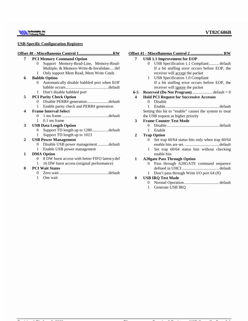
VT82C686B
Revision 1.71 June 9, 2000 -76- Function 2 Registers - USB Controller Ports 0-1
7HFKQRORJLHV ,QF'HOLYHULQJ 9DOXH'HOLYHULQJ 9DOXH
USB-Specific Configuration Registers
Offset 40 - Miscellaneous Control 1 ................................. RW7 PCI Memory Command Option
0 Support Memory-Read-Line, Memory-Read-Multiple, & Memory-Write-&-Invalidate.... def
1 Only support Mem Read, Mem Write Cmds6 Babble Option
0 Automatically disable babbled port when EOFbabble occurs..........................................default
1 Don’t disable babbled port5 PCI Parity Check Option
0 Disable PERR# generation.....................default1 Enable parity check and PERR# generation
4 Frame Interval Select0 1 ms frame..............................................default1 0.1 ms frame
3 USB Data Length Option0 Support TD length up to 1280................default1 Support TD length up to 1023
2 USB Power Management0 Disable USB power management...........default1 Enable USB power management
1 DMA Option0 8 DW burst access with better FIFO latencydef1 16 DW burst access (original performance)
0 PCI Wait States0 Zero wait ................................................default1 One wait
Offset 41 - Miscellaneous Control 2 ................................ RW7 USB 1.1 Improvement for EOP
0 USB Specification 1.1 Compliant.......... defaultIf a bit stuffing error occurs before EOP, thereceiver will accept the packet
1 USB Specification 1.0 CompliantIf a bit stuffing error occurs before EOP, thereceiver will ignore the packet
6-5 Reserved (Do Not Program) ....................default = 04 Hold PCI Request for Successive Accesses
0 Disable1 Enable .................................................... default
Setting this bit to “enable” causes the system to treatthe USB request as higher priority
3 Frame Counter Test Mode0 Disable................................................... default1 Enable
2 Trap Option0 Set trap 60/64 status bits only when trap 60/64
enable bits are set. ................................. default1 Set trap 60/64 status bits without checking
enable bits1 A20gate Pass Through Option
0 Pass through A20GATE command sequencedefined in UHCI .................................... default
1 Don’t pass through Write I/O port 64 (ff)0 USB IRQ Test Mode
0 Normal Operation .................................. default1 Generate USB IRQ
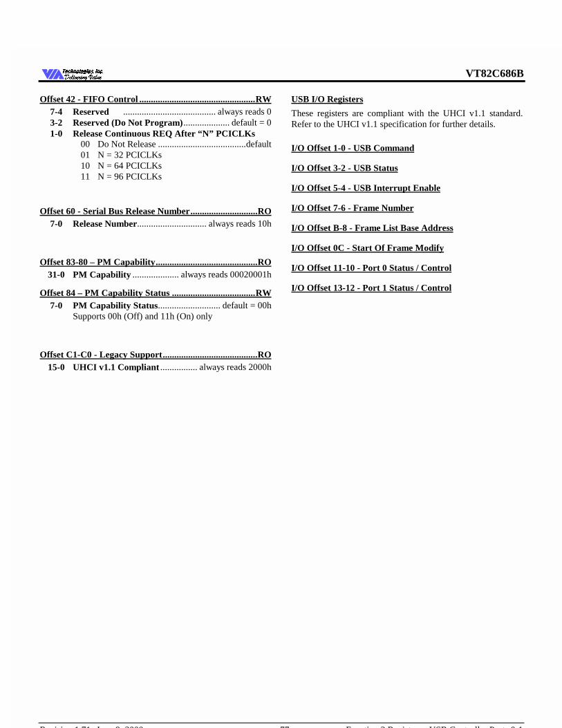
VT82C686B
Revision 1.71 June 9, 2000 -77- Function 2 Registers - USB Controller Ports 0-1
7HFKQRORJLHV ,QF'HOLYHULQJ 9DOXH'HOLYHULQJ 9DOXH
Offset 42 - FIFO Control .................................................. RW7-4 Reserved ........................................ always reads 03-2 Reserved (Do Not Program).................... default = 01-0 Release Continuous REQ After “N” PCICLKs
00 Do Not Release ......................................default01 N = 32 PCICLKs10 N = 64 PCICLKs11 N = 96 PCICLKs
Offset 60 - Serial Bus Release Number ............................. RO7-0 Release Number.............................. always reads 10h
Offset 83-80 – PM Capability ............................................ RO31-0 PM Capability .................... always reads 00020001h
Offset 84 – PM Capability Status .................................... RW7-0 PM Capability Status........................... default = 00h
Supports 00h (Off) and 11h (On) only
Offset C1-C0 - Legacy Support ......................................... RO15-0 UHCI v1.1 Compliant ................ always reads 2000h
USB I/O Registers
These registers are compliant with the UHCI v1.1 standard.Refer to the UHCI v1.1 specification for further details.
I/O Offset 1-0 - USB Command
I/O Offset 3-2 - USB Status
I/O Offset 5-4 - USB Interrupt Enable
I/O Offset 7-6 - Frame Number
I/O Offset B-8 - Frame List Base Address
I/O Offset 0C - Start Of Frame Modify
I/O Offset 11-10 - Port 0 Status / Control
I/O Offset 13-12 - Port 1 Status / Control
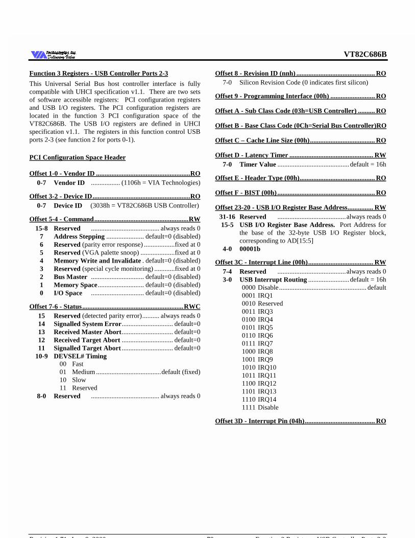
VT82C686B
Revision 1.71 June 9, 2000 -78- Function 3 Registers - USB Controller Ports 2-3
7HFKQRORJLHV ,QF'HOLYHULQJ 9DOXH'HOLYHULQJ 9DOXH
Function 3 Registers - USB Controller Ports 2-3
This Universal Serial Bus host controller interface is fullycompatible with UHCI specification v1.1. There are two setsof software accessible registers: PCI configuration registersand USB I/O registers. The PCI configuration registers arelocated in the function 3 PCI configuration space of theVT82C686B. The USB I/O registers are defined in UHCIspecification v1.1. The registers in this function control USBports 2-3 (see function 2 for ports 0-1).
PCI Configuration Space Header
Offset 1-0 - Vendor ID ....................................................... RO0-7 Vendor ID ................. (1106h = VIA Technologies)
Offset 3-2 - Device ID ......................................................... RO0-7 Device ID (3038h = VT82C686B USB Controller)
Offset 5-4 - Command ....................................................... RW15-8 Reserved ........................................ always reads 0
7 Address Stepping ...................... default=0 (disabled)6 Reserved (parity error response) ..................fixed at 05 Reserved (VGA palette snoop) ....................fixed at 04 Memory Write and Invalidate . default=0 (disabled)3 Reserved (special cycle monitoring) ............fixed at 02 Bus Master ............................... default=0 (disabled)1 Memory Space ........................... default=0 (disabled)0 I/O Space ............................... default=0 (disabled)
Offset 7-6 - Status ........................................................... RWC15 Reserved (detected parity error).......... always reads 014 Signalled System Error.............................. default=013 Received Master Abort.............................. default=012 Received Target Abort .............................. default=011 Signalled Target Abort .............................. default=0
10-9 DEVSEL# Timing00 Fast01 Medium ......................................default (fixed)10 Slow11 Reserved
8-0 Reserved ........................................ always reads 0
Offset 8 - Revision ID (nnh) .............................................. RO7-0 Silicon Revision Code (0 indicates first silicon)
Offset 9 - Programming Interface (00h) .......................... RO
Offset A - Sub Class Code (03h=USB Controller) .......... RO
Offset B - Base Class Code (0Ch=Serial Bus Controller) RO
Offset C – Cache Line Size (00h) ...................................... RO
Offset D - Latency Timer ................................................. RW7-0 Timer Value ..........................................default = 16h
Offset E - Header Type (00h) ............................................ RO
Offset F - BIST (00h) ......................................................... RO
Offset 23-20 - USB I/O Register Base Address ............... RW31-16 Reserved ........................................always reads 015-5 USB I/O Register Base Address. Port Address for
the base of the 32-byte USB I/O Register block,corresponding to AD[15:5]
4-0 00001b
Offset 3C - Interrupt Line (00h) ...................................... RW7-4 Reserved ........................................always reads 03-0 USB Interrupt Routing ........................default = 16h
0000 Disable................................................... default0001 IRQ10010 Reserved0011 IRQ30100 IRQ40101 IRQ50110 IRQ60111 IRQ71000 IRQ81001 IRQ91010 IRQ101011 IRQ111100 IRQ121101 IRQ131110 IRQ141111 Disable
Offset 3D - Interrupt Pin (04h) ......................................... RO

VT82C686B
Revision 1.71 June 9, 2000 -79- Function 3 Registers - USB Controller Ports 2-3
7HFKQRORJLHV ,QF'HOLYHULQJ 9DOXH'HOLYHULQJ 9DOXH
USB-Specific Configuration Registers
Offset 40 - Miscellaneous Control 1 ................................. RW7 PCI Memory Command Option
0 Support Memory-Read-Line, Memory-Read-Multiple, & Memory-Write-&-Invalidate.... def
1 Only support Mem Read, Mem Write Cmds6 Babble Option
0 Automatically disable babbled port when EOFbabble occurs..........................................default
1 Don’t disable babbled port5 PCI Parity Check Option
0 Disable PERR# generation.....................default1 Enable parity check and PERR# generation
4 Frame Interval Select0 1 ms frame..............................................default1 0.1 ms frame
3 USB Data Length Option0 Support TD length up to 1280................default1 Support TD length up to 1023
2 USB Power Management0 Disable USB power management...........default1 Enable USB power management
1 DMA Option0 8 DW burst access with better FIFO latencydef1 16 DW burst access (original performance)
0 PCI Wait States0 Zero wait ................................................default1 One wait
Offset 41 - Miscellaneous Control 2 ................................ RW7 USB 1.1 Improvement for EOP
0 USB Specification 1.1 Compliant.......... defaultIf a bit stuffing error occurs before EOP, thereceiver will accept the packet
1 USB Specification 1.0 CompliantIf a bit stuffing error occurs before EOP, thereceiver will ignore the packet
6-5 Reserved (Do Not Program) ....................default = 04 Hold PCI Request for Successive Accesses
0 Disable1 Enable .................................................... default
Setting this bit to “enable” causes the system to treatthe USB request as higher priority
3 Frame Counter Test Mode0 Disable................................................... default1 Enable
2 Trap Option0 Set trap 60/64 status bits only when trap 60/64
enable bits are set. ................................. default1 Set trap 60/64 status bits without checking
enable bits1 A20gate Pass Through Option
0 Pass through A20GATE command sequencedefined in UHCI .................................... default
1 Don’t pass through Write I/O port 64 (ff)0 USB IRQ Test Mode
0 Normal Operation .................................. default1 Generate USB IRQ
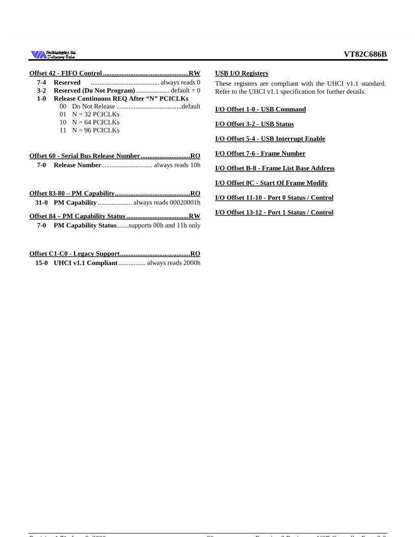
VT82C686B
Revision 1.71 June 9, 2000 -80- Function 3 Registers - USB Controller Ports 2-3
7HFKQRORJLHV ,QF'HOLYHULQJ 9DOXH'HOLYHULQJ 9DOXH
Offset 42 - FIFO Control .................................................. RW7-4 Reserved ........................................ always reads 03-2 Reserved (Do Not Program).................... default = 01-0 Release Continuous REQ After “N” PCICLKs
00 Do Not Release ......................................default01 N = 32 PCICLKs10 N = 64 PCICLKs11 N = 96 PCICLKs
Offset 60 - Serial Bus Release Number ............................. RO7-0 Release Number.............................. always reads 10h
Offset 83-80 – PM Capability ............................................ RO31-0 PM Capability .................... always reads 00020001h
Offset 84 – PM Capability Status .................................... RW7-0 PM Capability Status.......supports 00h and 11h only
Offset C1-C0 - Legacy Support ......................................... RO15-0 UHCI v1.1 Compliant ................ always reads 2000h
USB I/O Registers
These registers are compliant with the UHCI v1.1 standard.Refer to the UHCI v1.1 specification for further details.
I/O Offset 1-0 - USB Command
I/O Offset 3-2 - USB Status
I/O Offset 5-4 - USB Interrupt Enable
I/O Offset 7-6 - Frame Number
I/O Offset B-8 - Frame List Base Address
I/O Offset 0C - Start Of Frame Modify
I/O Offset 11-10 - Port 0 Status / Control
I/O Offset 13-12 - Port 1 Status / Control
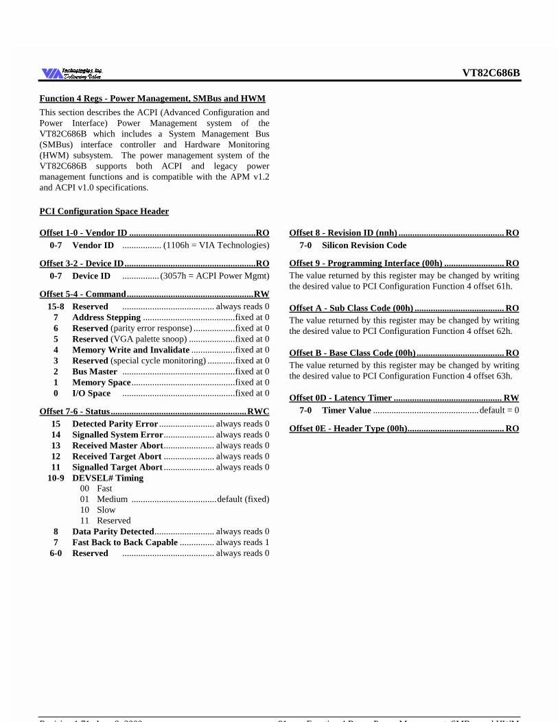
VT82C686B
Revision 1.71 June 9, 2000 -81- Function 4 Regs - Power Management, SMBus and HWM
7HFKQRORJLHV ,QF'HOLYHULQJ 9DOXH'HOLYHULQJ 9DOXH
Function 4 Regs - Power Management, SMBus and HWM
This section describes the ACPI (Advanced Configuration andPower Interface) Power Management system of theVT82C686B which includes a System Management Bus(SMBus) interface controller and Hardware Monitoring(HWM) subsystem. The power management system of theVT82C686B supports both ACPI and legacy powermanagement functions and is compatible with the APM v1.2and ACPI v1.0 specifications.
PCI Configuration Space Header
Offset 1-0 - Vendor ID ....................................................... RO0-7 Vendor ID ................. (1106h = VIA Technologies)
Offset 3-2 - Device ID ......................................................... RO0-7 Device ID ................ (3057h = ACPI Power Mgmt)
Offset 5-4 - Command ....................................................... RW15-8 Reserved ........................................ always reads 0
7 Address Stepping ........................................fixed at 06 Reserved (parity error response) ..................fixed at 05 Reserved (VGA palette snoop) ....................fixed at 04 Memory Write and Invalidate ...................fixed at 03 Reserved (special cycle monitoring) ............fixed at 02 Bus Master .................................................fixed at 01 Memory Space .............................................fixed at 00 I/O Space .................................................fixed at 0
Offset 7-6 - Status ........................................................... RWC15 Detected Parity Error ........................ always reads 014 Signalled System Error...................... always reads 013 Received Master Abort...................... always reads 012 Received Target Abort ...................... always reads 011 Signalled Target Abort ...................... always reads 0
10-9 DEVSEL# Timing00 Fast01 Medium .....................................default (fixed)10 Slow11 Reserved
8 Data Parity Detected.......................... always reads 07 Fast Back to Back Capable ............... always reads 1
6-0 Reserved ........................................ always reads 0
Offset 8 - Revision ID (nnh) .............................................. RO7-0 Silicon Revision Code
Offset 9 - Programming Interface (00h) .......................... ROThe value returned by this register may be changed by writingthe desired value to PCI Configuration Function 4 offset 61h.
Offset A - Sub Class Code (00h) ....................................... ROThe value returned by this register may be changed by writingthe desired value to PCI Configuration Function 4 offset 62h.
Offset B - Base Class Code (00h) ...................................... ROThe value returned by this register may be changed by writingthe desired value to PCI Configuration Function 4 offset 63h.
Offset 0D - Latency Timer ............................................... RW7-0 Timer Value ..............................................default = 0
Offset 0E - Header Type (00h) .......................................... RO
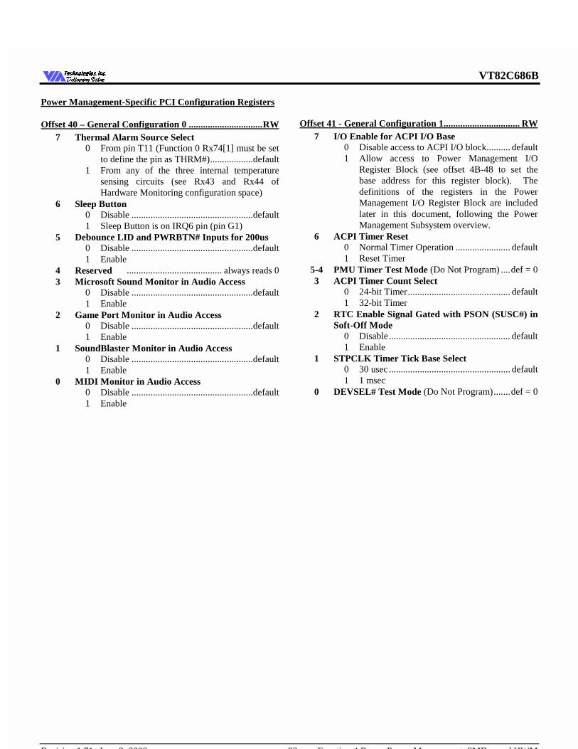
VT82C686B
Revision 1.71 June 9, 2000 -82- Function 4 Regs - Power Management, SMBus and HWM
7HFKQRORJLHV ,QF'HOLYHULQJ 9DOXH'HOLYHULQJ 9DOXH
Power Management-Specific PCI Configuration Registers
Offset 40 – General Configuration 0 ............................... RW7 Thermal Alarm Source Select
0 From pin T11 (Function 0 Rx74[1] must be setto define the pin as THRM#)..................default
1 From any of the three internal temperaturesensing circuits (see Rx43 and Rx44 ofHardware Monitoring configuration space)
6 Sleep Button0 Disable ...................................................default1 Sleep Button is on IRQ6 pin (pin G1)
5 Debounce LID and PWRBTN# Inputs for 200us0 Disable ...................................................default1 Enable
4 Reserved ........................................ always reads 03 Microsoft Sound Monitor in Audio Access
0 Disable ...................................................default1 Enable
2 Game Port Monitor in Audio Access0 Disable ...................................................default1 Enable
1 SoundBlaster Monitor in Audio Access0 Disable ...................................................default1 Enable
0 MIDI Monitor in Audio Access0 Disable ...................................................default1 Enable
Offset 41 - General Configuration 1 ................................ RW7 I/O Enable for ACPI I/O Base
0 Disable access to ACPI I/O block.......... default1 Allow access to Power Management I/O
Register Block (see offset 4B-48 to set thebase address for this register block). Thedefinitions of the registers in the PowerManagement I/O Register Block are includedlater in this document, following the PowerManagement Subsystem overview.
6 ACPI Timer Reset0 Normal Timer Operation ....................... default1 Reset Timer
5-4 PMU Timer Test Mode (Do Not Program) ....def = 03 ACPI Timer Count Select
0 24-bit Timer........................................... default1 32-bit Timer
2 RTC Enable Signal Gated with PSON (SUSC#) inSoft-Off Mode
0 Disable................................................... default1 Enable
1 STPCLK Timer Tick Base Select0 30 usec ................................................... default1 1 msec
0 DEVSEL# Test Mode (Do Not Program).......def = 0
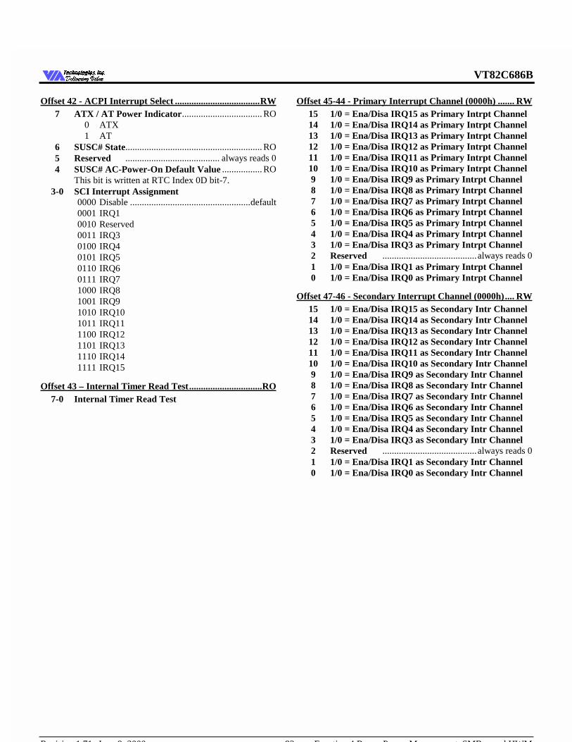
VT82C686B
Revision 1.71 June 9, 2000 -83- Function 4 Regs - Power Management, SMBus and HWM
7HFKQRORJLHV ,QF'HOLYHULQJ 9DOXH'HOLYHULQJ 9DOXH
Offset 42 - ACPI Interrupt Select .................................... RW7 ATX / AT Power Indicator.................................. RO
0 ATX1 AT
6 SUSC# State.......................................................... RO5 Reserved ........................................ always reads 04 SUSC# AC-Power-On Default Value ................. RO
This bit is written at RTC Index 0D bit-7.3-0 SCI Interrupt Assignment
0000 Disable ...................................................default0001 IRQ10010 Reserved0011 IRQ30100 IRQ40101 IRQ50110 IRQ60111 IRQ71000 IRQ81001 IRQ91010 IRQ101011 IRQ111100 IRQ121101 IRQ131110 IRQ141111 IRQ15
Offset 43 – Internal Timer Read Test ............................... RO7-0 Internal Timer Read Test
Offset 45-44 - Primary Interrupt Channel (0000h) ....... RW15 1/0 = Ena/Disa IRQ15 as Primary Intrpt Channel14 1/0 = Ena/Disa IRQ14 as Primary Intrpt Channel13 1/0 = Ena/Disa IRQ13 as Primary Intrpt Channel12 1/0 = Ena/Disa IRQ12 as Primary Intrpt Channel11 1/0 = Ena/Disa IRQ11 as Primary Intrpt Channel10 1/0 = Ena/Disa IRQ10 as Primary Intrpt Channel9 1/0 = Ena/Disa IRQ9 as Primary Intrpt Channel8 1/0 = Ena/Disa IRQ8 as Primary Intrpt Channel7 1/0 = Ena/Disa IRQ7 as Primary Intrpt Channel6 1/0 = Ena/Disa IRQ6 as Primary Intrpt Channel5 1/0 = Ena/Disa IRQ5 as Primary Intrpt Channel4 1/0 = Ena/Disa IRQ4 as Primary Intrpt Channel3 1/0 = Ena/Disa IRQ3 as Primary Intrpt Channel2 Reserved ........................................always reads 01 1/0 = Ena/Disa IRQ1 as Primary Intrpt Channel0 1/0 = Ena/Disa IRQ0 as Primary Intrpt Channel
Offset 47-46 - Secondary Interrupt Channel (0000h) .... RW15 1/0 = Ena/Disa IRQ15 as Secondary Intr Channel14 1/0 = Ena/Disa IRQ14 as Secondary Intr Channel13 1/0 = Ena/Disa IRQ13 as Secondary Intr Channel12 1/0 = Ena/Disa IRQ12 as Secondary Intr Channel11 1/0 = Ena/Disa IRQ11 as Secondary Intr Channel10 1/0 = Ena/Disa IRQ10 as Secondary Intr Channel9 1/0 = Ena/Disa IRQ9 as Secondary Intr Channel8 1/0 = Ena/Disa IRQ8 as Secondary Intr Channel7 1/0 = Ena/Disa IRQ7 as Secondary Intr Channel6 1/0 = Ena/Disa IRQ6 as Secondary Intr Channel5 1/0 = Ena/Disa IRQ5 as Secondary Intr Channel4 1/0 = Ena/Disa IRQ4 as Secondary Intr Channel3 1/0 = Ena/Disa IRQ3 as Secondary Intr Channel2 Reserved ........................................always reads 01 1/0 = Ena/Disa IRQ1 as Secondary Intr Channel0 1/0 = Ena/Disa IRQ0 as Secondary Intr Channel
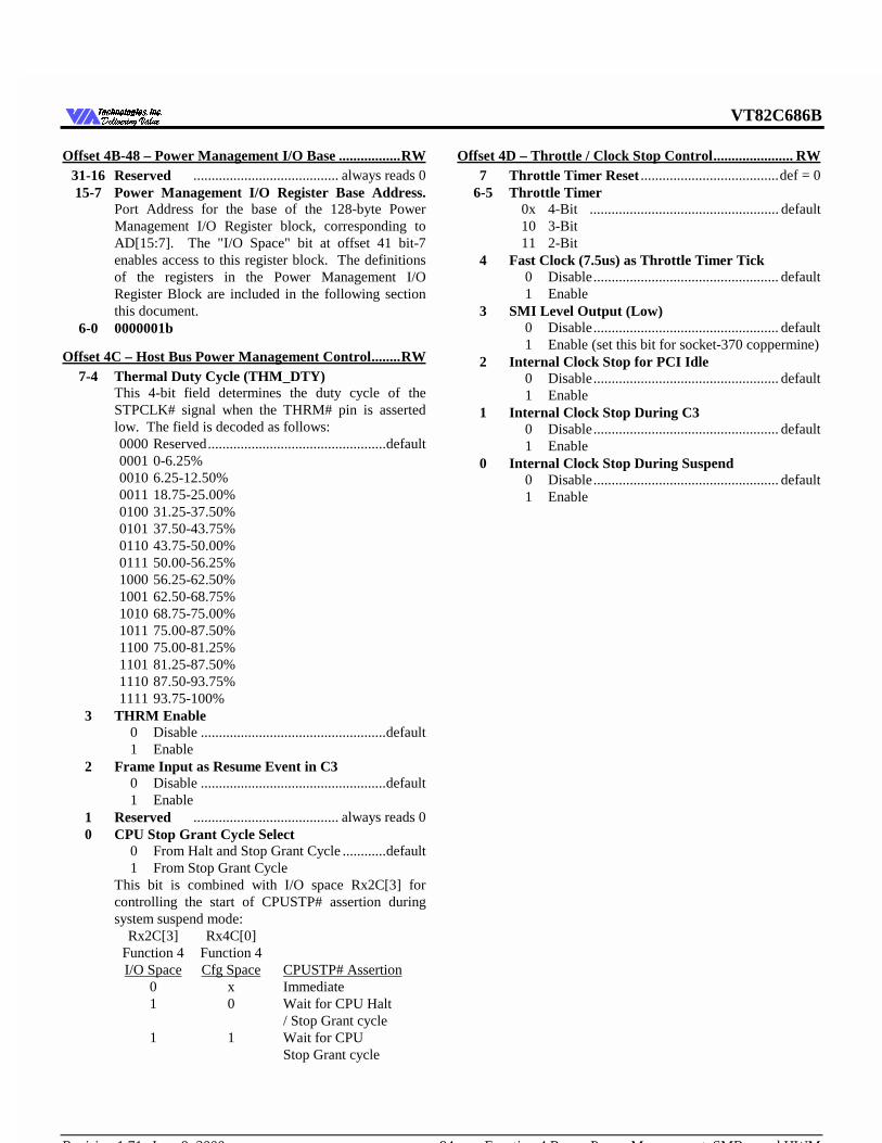
VT82C686B
Revision 1.71 June 9, 2000 -84- Function 4 Regs - Power Management, SMBus and HWM
7HFKQRORJLHV ,QF'HOLYHULQJ 9DOXH'HOLYHULQJ 9DOXH
Offset 4B-48 – Power Management I/O Base ................. RW31-16 Reserved ........................................ always reads 015-7 Power Management I/O Register Base Address.
Port Address for the base of the 128-byte PowerManagement I/O Register block, corresponding toAD[15:7]. The "I/O Space" bit at offset 41 bit-7enables access to this register block. The definitionsof the registers in the Power Management I/ORegister Block are included in the following sectionthis document.
6-0 0000001b
Offset 4C – Host Bus Power Management Control ........ RW7-4 Thermal Duty Cycle (THM_DTY)
This 4-bit field determines the duty cycle of theSTPCLK# signal when the THRM# pin is assertedlow. The field is decoded as follows:0000 Reserved.................................................default0001 0-6.25%0010 6.25-12.50%0011 18.75-25.00%0100 31.25-37.50%0101 37.50-43.75%0110 43.75-50.00%0111 50.00-56.25%1000 56.25-62.50%1001 62.50-68.75%1010 68.75-75.00%1011 75.00-87.50%1100 75.00-81.25%1101 81.25-87.50%1110 87.50-93.75%1111 93.75-100%
3 THRM Enable0 Disable ...................................................default1 Enable
2 Frame Input as Resume Event in C30 Disable ...................................................default1 Enable
1 Reserved ........................................ always reads 00 CPU Stop Grant Cycle Select
0 From Halt and Stop Grant Cycle ............default1 From Stop Grant Cycle
This bit is combined with I/O space Rx2C[3] forcontrolling the start of CPUSTP# assertion duringsystem suspend mode:
Rx2C[3] Rx4C[0]Function 4 Function 4I/O Space Cfg Space CPUSTP# Assertion
0 x Immediate1 0 Wait for CPU Halt
/ Stop Grant cycle1 1 Wait for CPU
Stop Grant cycle
Offset 4D – Throttle / Clock Stop Control ...................... RW7 Throttle Timer Reset ......................................def = 0
6-5 Throttle Timer0x 4-Bit .................................................... default10 3-Bit11 2-Bit
4 Fast Clock (7.5us) as Throttle Timer Tick0 Disable................................................... default1 Enable
3 SMI Level Output (Low)0 Disable................................................... default1 Enable (set this bit for socket-370 coppermine)
2 Internal Clock Stop for PCI Idle0 Disable................................................... default1 Enable
1 Internal Clock Stop During C30 Disable................................................... default1 Enable
0 Internal Clock Stop During Suspend0 Disable................................................... default1 Enable
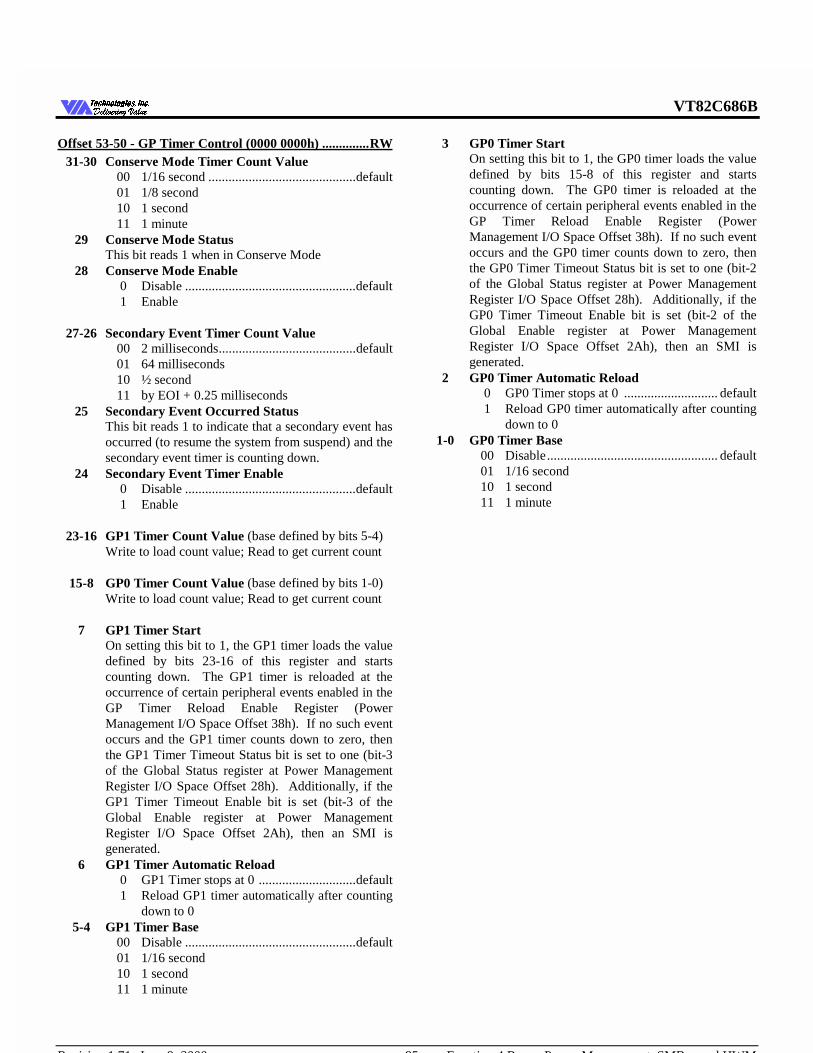
VT82C686B
Revision 1.71 June 9, 2000 -85- Function 4 Regs - Power Management, SMBus and HWM
7HFKQRORJLHV ,QF'HOLYHULQJ 9DOXH'HOLYHULQJ 9DOXH
Offset 53-50 - GP Timer Control (0000 0000h) .............. RW31-30 Conserve Mode Timer Count Value
00 1/16 second ............................................default01 1/8 second10 1 second11 1 minute
29 Conserve Mode StatusThis bit reads 1 when in Conserve Mode
28 Conserve Mode Enable0 Disable ...................................................default1 Enable
27-26 Secondary Event Timer Count Value00 2 milliseconds.........................................default01 64 milliseconds10 ½ second11 by EOI + 0.25 milliseconds
25 Secondary Event Occurred StatusThis bit reads 1 to indicate that a secondary event hasoccurred (to resume the system from suspend) and thesecondary event timer is counting down.
24 Secondary Event Timer Enable0 Disable ...................................................default1 Enable
23-16 GP1 Timer Count Value (base defined by bits 5-4)Write to load count value; Read to get current count
15-8 GP0 Timer Count Value (base defined by bits 1-0)Write to load count value; Read to get current count
7 GP1 Timer StartOn setting this bit to 1, the GP1 timer loads the valuedefined by bits 23-16 of this register and startscounting down. The GP1 timer is reloaded at theoccurrence of certain peripheral events enabled in theGP Timer Reload Enable Register (PowerManagement I/O Space Offset 38h). If no such eventoccurs and the GP1 timer counts down to zero, thenthe GP1 Timer Timeout Status bit is set to one (bit-3of the Global Status register at Power ManagementRegister I/O Space Offset 28h). Additionally, if theGP1 Timer Timeout Enable bit is set (bit-3 of theGlobal Enable register at Power ManagementRegister I/O Space Offset 2Ah), then an SMI isgenerated.
6 GP1 Timer Automatic Reload0 GP1 Timer stops at 0 .............................default1 Reload GP1 timer automatically after counting
down to 05-4 GP1 Timer Base
00 Disable ...................................................default01 1/16 second10 1 second11 1 minute
3 GP0 Timer StartOn setting this bit to 1, the GP0 timer loads the valuedefined by bits 15-8 of this register and startscounting down. The GP0 timer is reloaded at theoccurrence of certain peripheral events enabled in theGP Timer Reload Enable Register (PowerManagement I/O Space Offset 38h). If no such eventoccurs and the GP0 timer counts down to zero, thenthe GP0 Timer Timeout Status bit is set to one (bit-2of the Global Status register at Power ManagementRegister I/O Space Offset 28h). Additionally, if theGP0 Timer Timeout Enable bit is set (bit-2 of theGlobal Enable register at Power ManagementRegister I/O Space Offset 2Ah), then an SMI isgenerated.
2 GP0 Timer Automatic Reload0 GP0 Timer stops at 0 ............................ default1 Reload GP0 timer automatically after counting
down to 01-0 GP0 Timer Base
00 Disable................................................... default01 1/16 second10 1 second11 1 minute
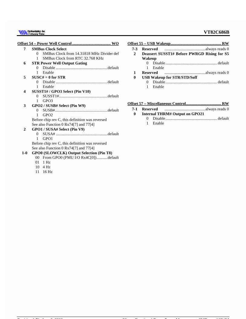
VT82C686B
Revision 1.71 June 9, 2000 -86- Function 4 Regs - Power Management, SMBus and HWM
7HFKQRORJLHV ,QF'HOLYHULQJ 9DOXH'HOLYHULQJ 9DOXH
Offset 54 – Power Well Control ...................................... WO7 SMBus Clock Select
0 SMBus Clock from 14.31818 MHz Divider def1 SMBus Clock from RTC 32.768 KHz
6 STR Power Well Output Gating0 Disable ...................................................default1 Enable
5 SUSC# = 0 for STR0 Disable ...................................................default1 Enable
4 SUSST1# / GPO3 Select (Pin V10)0 SUSST1#................................................default1 GPO3
3 GPO2 / SUSB# Select (Pin W9)0 SUSB#....................................................default1 GPO2
Before chip rev C, this definition was reversedSee also Function 0 Rx74[7] and 77[4]
2 GPO1 / SUSA# Select (Pin V9)0 SUSA# ...................................................default1 GPO1
Before chip rev C, this definition was reversedSee also Function 0 Rx74[7] and 77[4]
1-0 GPO0 (SLOWCLK) Output Selection (Pin T8)00 From GPO0 (PMU I/O Rx4C[0])...........default01 1 Hz10 4 Hz11 16 Hz
Offset 55 – USB Wakeup .................................................. RW7-3 Reserved ........................................always reads 02 Deassert SUSST1# Before PWRGD Rising for S5
Wakeup0 Disable................................................... default1 Enable
1 Reserved ........................................always reads 00 USB Wakeup for STR/STD/Soff
0 Disable................................................... default1 Enable
Offset 57 – Miscellaneous Control................................... RW7-1 Reserved ........................................always reads 00 Internal THRM# Output on GPO21
0 Disable................................................... default1 Enable
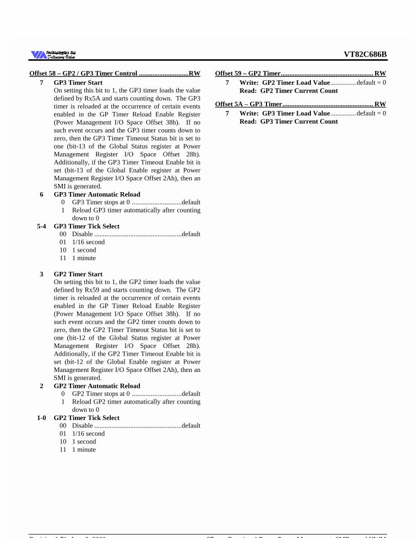
VT82C686B
Revision 1.71 June 9, 2000 -87- Function 4 Regs - Power Management, SMBus and HWM
7HFKQRORJLHV ,QF'HOLYHULQJ 9DOXH'HOLYHULQJ 9DOXH
Offset 58 – GP2 / GP3 Timer Control ............................. RW7 GP3 Timer Start
On setting this bit to 1, the GP3 timer loads the valuedefined by Rx5A and starts counting down. The GP3timer is reloaded at the occurrence of certain eventsenabled in the GP Timer Reload Enable Register(Power Management I/O Space Offset 38h). If nosuch event occurs and the GP3 timer counts down tozero, then the GP3 Timer Timeout Status bit is set toone (bit-13 of the Global Status register at PowerManagement Register I/O Space Offset 28h).Additionally, if the GP3 Timer Timeout Enable bit isset (bit-13 of the Global Enable register at PowerManagement Register I/O Space Offset 2Ah), then anSMI is generated.
6 GP3 Timer Automatic Reload0 GP3 Timer stops at 0 .............................default1 Reload GP3 timer automatically after counting
down to 05-4 GP3 Timer Tick Select
00 Disable ...................................................default01 1/16 second10 1 second11 1 minute
3 GP2 Timer StartOn setting this bit to 1, the GP2 timer loads the valuedefined by Rx59 and starts counting down. The GP2timer is reloaded at the occurrence of certain eventsenabled in the GP Timer Reload Enable Register(Power Management I/O Space Offset 38h). If nosuch event occurs and the GP2 timer counts down tozero, then the GP2 Timer Timeout Status bit is set toone (bit-12 of the Global Status register at PowerManagement Register I/O Space Offset 28h).Additionally, if the GP2 Timer Timeout Enable bit isset (bit-12 of the Global Enable register at PowerManagement Register I/O Space Offset 2Ah), then anSMI is generated.
2 GP2 Timer Automatic Reload0 GP2 Timer stops at 0 .............................default1 Reload GP2 timer automatically after counting
down to 01-0 GP2 Timer Tick Select
00 Disable ...................................................default01 1/16 second10 1 second11 1 minute
Offset 59 – GP2 Timer ...................................................... RW7 Write: GP2 Timer Load Value...............default = 0
Read: GP2 Timer Current Count
Offset 5A – GP3 Timer ..................................................... RW7 Write: GP3 Timer Load Value...............default = 0
Read: GP3 Timer Current Count
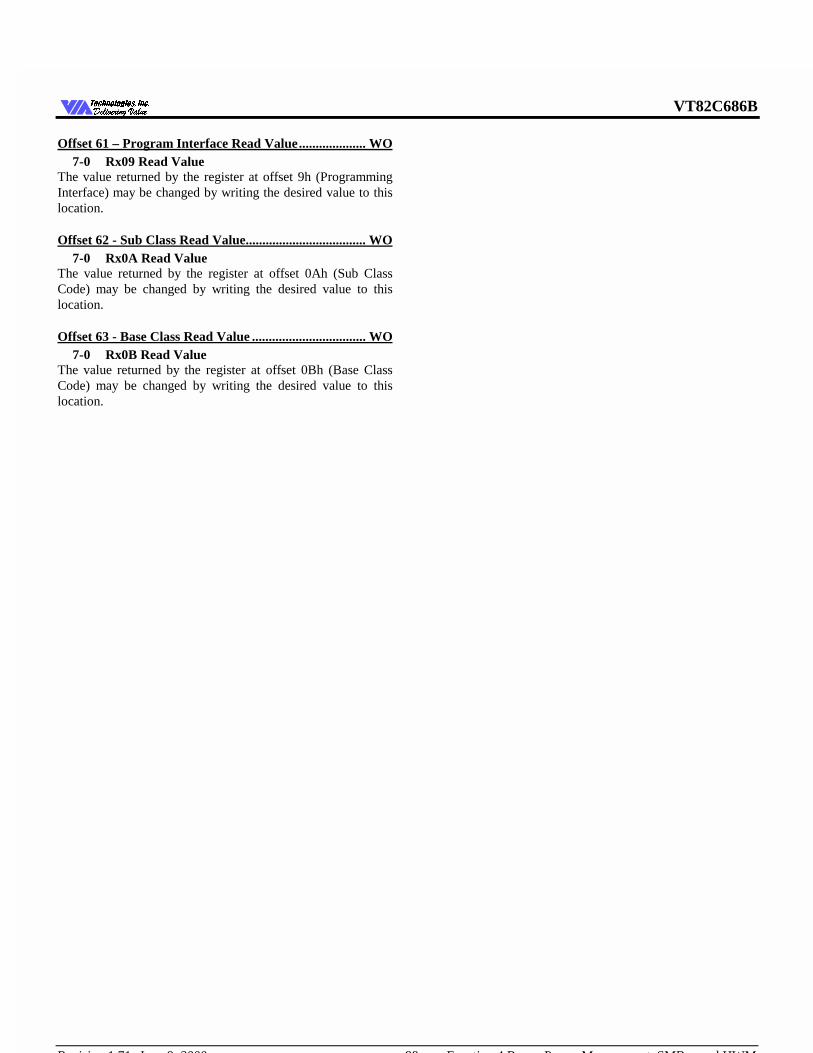
VT82C686B
Revision 1.71 June 9, 2000 -88- Function 4 Regs - Power Management, SMBus and HWM
7HFKQRORJLHV ,QF'HOLYHULQJ 9DOXH'HOLYHULQJ 9DOXH
Offset 61 – Program Interface Read Value .................... WO7-0 Rx09 Read Value
The value returned by the register at offset 9h (ProgrammingInterface) may be changed by writing the desired value to thislocation.
Offset 62 - Sub Class Read Value.................................... WO7-0 Rx0A Read Value
The value returned by the register at offset 0Ah (Sub ClassCode) may be changed by writing the desired value to thislocation.
Offset 63 - Base Class Read Value .................................. WO7-0 Rx0B Read Value
The value returned by the register at offset 0Bh (Base ClassCode) may be changed by writing the desired value to thislocation.

VT82C686B
Revision 1.71 June 9, 2000 -89- Function 4 Regs - Power Management, SMBus and HWM
7HFKQRORJLHV ,QF'HOLYHULQJ 9DOXH'HOLYHULQJ 9DOXH
Hardware-Monitor-Specific Configuration Registers
Offset 71-70 – Hardware Monitor I/O Base ................... RW15-7 I/O Base (128-byte I/O space) ................. default = 06-0 Fixed .......................... always reads 0000001b
Offset 74 –Hardware Monitor Control ........................... RW7-4 Reserved ........................................ always reads 03 Hardware Monitoring Interrupt
0 SMI .....................................................default1 SCI
2-1 Reserved ........................................ always reads 00 Hardware Monitoring I/O Enable
0 Disable hardware monitor functions.......default1 Enable hardware monitor functions
System Management Bus-Specific Configuration Registers
Offset 93-90 – SMBus I/O Base ....................................... RW31-16 Reserved ........................................always reads 015-4 I/O Base (16-byte I/O space)................default = 00h3-0 Fixed ................................always reads 0001b
Offset D2 – SMBus Host Configuration ......................... RW7-4 Reserved ........................................always reads 03 SMBus Interrupt Select
0 SMI .................................................... default1 SCI
2 SMBus Clock Select0 Divide down from 14.31818 MHz......... default1 64 KHz derived from 32.768 KHz RTC clock
1 SMBus IRQ0 Disable................................................... default1 Enable
0 SMBus Host Controller Enable0 Disable SMB controller functions ......... default1 Enable SMB controller functions
Offset D3 – SMBus Host Slave Command ...................... RW7-0 SMBus Host Slave Command Code ..........default=0
Offset D4 – SMBus Slave Address for Port 1 ................. RW7-0 SMBus Slave Address for Port 1...............default=0
Bit-0 must be set to 0 for proper operation
Offset D5 – SMBus Slave Address for Port 2 ................. RW7-0 SMBus Slave Address for Port 2...............default=0
Bit-0 must be set to 0 for proper operation
Offset D6 – SMBus Revision ID ....................................... RO7-0 SMBus Revision Code
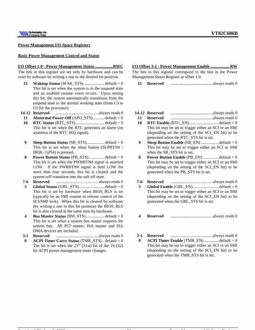
VT82C686B
Revision 1.71 June 9, 2000 -90- Power Management I/O-Space Registers
7HFKQRORJLHV ,QF'HOLYHULQJ 9DOXH'HOLYHULQJ 9DOXH
Power Management I/O-Space Registers
Basic Power Management Control and Status
I/O Offset 1-0 - Power Management Status ................. RWCThe bits in this register are set only by hardware and can bereset by software by writing a one to the desired bit position.
15 Wakeup Status (WAK_STS) ................... default = 0This bit is set when the system is in the suspend stateand an enabled resume event occurs. Upon settingthis bit, the system automatically transitions from thesuspend state to the normal working state (from C3 toC0 for the processor).
14-12 Reserved ........................................ always reads 011 Abnormal Power-Off (APO_STS)........... default = 010 RTC Status (RTC_STS) ........................... default = 0
This bit is set when the RTC generates an alarm (onassertion of the RTC IRQ signal).
9 Sleep Button Status (SB_STS)................. default = 0This bit is set when the sleep button (SLPBTN# /IRQ6 / GPI4) is pressed.
8 Power Button Status (PB_STS)............... default = 0This bit is set when the PWRBTN# signal is assertedLOW. If the PWRBTN# signal is held LOW formore than four seconds, this bit is cleared and thesystem will transition into the soft off state.
7-6 Reserved ........................................ always reads 05 Global Status (GBL_STS)........................ default = 0
This bit is set by hardware when BIOS_RLS is set(typically by an SMI routine to release control of theSCI/SMI lock). When this bit is cleared by software(by writing a one to this bit position) the BIOS_RLSbit is also cleared at the same time by hardware.
4 Bus Master Status (BM_STS) ................. default = 0This bit is set when a system bus master requests thesystem bus. All PCI master, ISA master and ISADMA devices are included.
3-1 Reserved ........................................ always reads 00 ACPI Timer Carry Status (TMR_STS) .. default = 0
The bit is set when the 23rd (31st) bit of the 24 (32)bit ACPI power management timer changes.
I/O Offset 3-2 - Power Management Enable .................. RWThe bits in this register correspond to the bits in the PowerManagement Status Register at offset 1-0.
15 Reserved ........................................always reads 0
14-12 Reserved ........................................always reads 011 Reserved ........................................always reads 010 RTC Enable (RTC_EN)............................default = 0
This bit may be set to trigger either an SCI or an SMI(depending on the setting of the SCI_EN bit) to begenerated when the RTC_STS bit is set.
9 Sleep Button Enable (SB_EN) .................default = 0This bit may be set to trigger either an SCI or SMIwhen the SB_STS bit is set.
8 Power Button Enable (PB_EN) ...............default = 0This bit may be set to trigger either an SCI or an SMI(depending on the setting of the SCI_EN bit) to begenerated when the PB_STS bit is set.
7-6 Reserved ........................................always reads 05 Global Enable (GBL_EN).........................default = 0
This bit may be set to trigger either an SCI or an SMI(depending on the setting of the SCI_EN bit) to begenerated when the GBL_STS bit is set.
4 Reserved ........................................always reads 0
3-1 Reserved ........................................always reads 00 ACPI Timer Enable (TMR_EN) ..............default = 0
This bit may be set to trigger either an SCI or an SMI(depending on the setting of the SCI_EN bit) to begenerated when the TMR_STS bit is set.
VT82C686B
Revision 1.71 June 9, 2000 -91- Power Management I/O-Space Registers
7HFKQRORJLHV ,QF'HOLYHULQJ 9DOXH'HOLYHULQJ 9DOXH
I/O Offset 5-4 - Power Management Control ................. RW15 Soft Resume14 Reserved ........................................ always reads 013 Sleep Enable (SLP_EN)...................... always reads 0
This is a write-only bit; reads from this bit alwaysreturn zero. Writing a one to this bit causes thesystem to sequence into the sleep (suspend) statedefined by the SLP_TYP field.
12-10 Sleep Type (SLP_TYP)000 Normal On001 Suspend to RAM (STR)010 Suspend to Disk (STD) (also called Soft Off).
The VCC power plane is turned off while theVCCS and VBAT planes remain on.
011 Reserved100 Power On Suspend without Reset101 Power On Suspend with CPU Reset110 Power On Suspend with CPU/PCI Reset111 Reserved
In any sleep state, there is minimal interface betweenpowered and non-powered planes so that the effortfor hardware design may be well managed.
9 Reserved ........................................ always reads 08 STD Command Generates System Reset Only
0 Disable ...................................................default1 Enable
7-3 Reserved ........................................ always reads 02 Global Release (GBL_RLS) ............ WO, default = 0
This bit is set by ACPI software to indicate therelease of the SCI / SMI lock. Upon setting of thisbit, the hardware automatically sets the BIOS_STSbit. The bit is cleared by hardware when theBIOS_STS bit is cleared by software. Note that thesetting of this bit will cause an SMI to be generated ifthe BIOS_EN bit is set (bit-5 of the Global Enableregister at offset 2Ah).
1 Bus Master Reload (BMS_RLD)0 Bus master requests are ignored by power
management logic...................................default1 Bus master requests transition the processor
from the C3 state to the C0 state0 SCI Enable (SCI_EN)
Selects the power management event to generateeither an SCI or SMI (for Power / Sleep Buttons &RTC only)
0 Generate SMI .........................................default1 Generate SCI
Note that certain power management events can beprogrammed individually to generate an SCI or SMIindependent of the setting of this bit (refer to theGeneral Purpose SCI Enable and General PurposeSMI Enable registers at offsets 22 and 24). Also,TMR_STS & GBL_STS always generate SCI andBIOS_STS always generates SMI.
I/O Offset 0B-08 - Power Management Timer ............... RW31-24 Extended Timer Value (ETM_VAL)
This field reads back 0 if the 24-bit timer option isselected (Rx41 bit-3).
23-0 Timer Value (TMR_VAL)This read-only field returns the running count of thepower management timer. This is a 24/32-bit counterthat runs off a 3.579545 MHz clock, and counts whilein the S0 (working) system state. The timer is reset toan initial value of zero during a reset, and thencontinues counting until the 14.31818 MHz input tothe chip is stopped. If the clock is restarted without areset, then the counter will continue counting fromwhere it stopped.
VT82C686B
Revision 1.71 June 9, 2000 -92- Power Management I/O-Space Registers
7HFKQRORJLHV ,QF'HOLYHULQJ 9DOXH'HOLYHULQJ 9DOXH
Processor Power Management Registers
I/O Offset 13-10 - Processor & PCI Bus Control............ RW31-12 Reserved ........................................ always reads 0
11 PCI Stop (PCISTP# asserted) when PCKRUN# isDeasserted (PCI_STP)
0 Enable.....................................................default1 Disable
10 PCI Bus Clock Run Without Stop (PCI_RUN)0 PCKRUN# will be de-activated after the PCI
bus is idle for 26 clocks..........................default1 PCKRUN# is always asserted
9 Host Clock Stop Enable (HOST_STP)0 STPCLK# will be asserted in the C3 state, but
the CPU clock is not stopped .................default1 CPU clock is stopped in the C3 state
8 Assert SLP# for Processor Level 3 Read0 Disable ...................................................default1 Enable
Used in Slot-1 systems only.7-5 Reserved ........................................ always reads 04 Throttling Enable (THT_EN)
Setting this bit starts clock throttling (modulating theSTPCLK# signal) regardless of the CPU state. Thethrottling duty cycle is determined by bits 3-0 of thisregister.
3-0 Throttling Duty Cycle (THT_DTY)This 4-bit field determines the duty cycle of theSTPCLK# signal when the system is in throttlingmode (the "Throttling Enable" bit is set to one). Theduty cycle indicates the percentage of time theSTPCLK# signal is asserted while the ThrottlingEnable bit is set. The field is decoded as follows:0000 Reserved0001 0-6.25%0010 6.25-12.50%0011 18.75-25.00%0100 31.25-37.50%0101 37.50-43.75%0110 43.75-50.00%0111 50.00-56.25%1000 56.25-62.50%1001 62.50-68.75%1010 68.75-75.00%1011 75.00-87.50%1100 75.00-81.25%1101 81.25-87.50%1110 87.50-93.75%1111 93.75-100%
I/O Offset 14 - Processor Level 2 ...................................... RO7-0 Level 2 ........................................always reads 0
Reads from this register put the processor into theStop Grant state (the VT82C686B asserts STPCLK#to suspend the processor). Wake up from Stop Grantstate is by interrupt (INTR, SMI, and SCI).
Reads from this register return all zeros; writes to this registerhave no effect.
I/O Offset 15 - Processor Level 3 ...................................... RO7-0 Level 3 ........................................always reads 0
Reads from this register put the processor in the C3clock state with the STPCLK# signal asserted. IfRx10[9] = 1 then the CPU clock is also stopped byasserting CPUSTP#. Wakeup from the C3 state is byinterrupt (INTR, SMI, and SCI).
Reads from this register return all zeros; writes to this registerhave no effect.
VT82C686B
Revision 1.71 June 9, 2000 -93- Power Management I/O-Space Registers
7HFKQRORJLHV ,QF'HOLYHULQJ 9DOXH'HOLYHULQJ 9DOXH
General Purpose Power Management Registers
I/O Offset 21-20 - General Purpose Status (GP_STS) . RWC15 Reserved ........................................ always reads 014 USB Wake-Up Status (UWAK_STS)
For STR / STD / Soff13 AC97 Wake-Up Status (AWAK_STS)
Can be set only in suspend mode12 Battery Low Status (BL_STS)
This bit is set when the BATLOW# input is assertedlow.
11 Notebook Lid Status (LID_STS)This bit is set when the LID input detects the edgeselected by Rx2C bit-7 (0=rising, 1=falling).
10 Thermal Detect Status (THRM_STS)This bit is set when the THRM input detects the edgeselected by Rx2C bit-6 (0=rising, 1=falling).
9 USB Resume Status (USB_STS)This bit is set when a USB peripheral generates aresume event.
8 Ring Status (RING_STS)This bit is set when the RING# input is asserted low.
7 GPI18 Toggle Status (GPI18_STS)This bit is set when the GPI18 pin is toggled.
6 GPI6 / EXTSMI6 Toggle Status (GPI6_STS)This bit is set when the GPI6 pin is toggled.
5 GPI5 Toggle Status (GPI5_STS)This bit is set when the GPI5 pin is toggled.
4 GPI4 / EXTSMI4 Toggle Status (GPI4_STS)This bit is set when the GPI4 pin is toggled.
3 GPI17 Toggle Status (GPI17_STS)This bit is set when the GPI17 pin is toggled.
2 GPI16 Toggle Status (GPI16_STS)This bit is set when the GPI16 pin is toggled.
1 GPI1 Toggle Status (GPI1_STS)This bit is set when the GPI1 pin is toggled.
0 EXTSMI# Status (EXT_STS)This bit is set when the EXTSMI# pin is asserted low.
Note that the above bits correspond one for one with the bitsof the General Purpose SCI Enable and General Purpose SMIEnable registers at offsets 22 and 24: an SCI or SMI isgenerated if the corresponding bit of the General Purpose SCIor SMI Enable registers, respectively, is set to one.
The above bits are set by hardware only and can only becleared by writing a one to the desired bit.
I/O Offset 23-22 - General Purpose SCI Enable ............ RW15 Reserved ........................................always reads 014 Enable SCI on setting of the UWAK_STS bit def=013 Enable SCI on setting of the AWAK_STS bit def=012 Enable SCI on setting of the BL_STS bit ......def=011 Enable SCI on setting of the LID_STS bit .....def=010 Enable SCI on setting of the THRM_STS bit def=09 Enable SCI on setting of the USB_STS bit ....def=08 Enable SCI on setting of the RING_STS bit .def=07 Enable SCI on setting of the GPI18_STS bit..def=06 Enable SCI on setting of the GPI6_STS bit....def=05 Enable SCI on setting of the GPI5_STS bit....def=04 Enable SCI on setting of the GPI4_STS bit....def=03 Enable SCI on setting of the GPI17_STS bit..def=02 Enable SCI on setting of the GPI16_STS bit..def=01 Enable SCI on setting of the GPI1_STS bit....def=00 Enable SCI on setting of the EXT_STS bit ....def=0
These bits allow generation of an SCI using a separate set ofconditions from those used for generating an SMI.
I/O Offset 25-24 - General Purpose SMI Enable ........... RW15-14 Reserved ........................................always reads 0
13 Enable SMI on setting of the AWAK_STS bit def=012 Enable SMI on setting of the BL_STS bit .....def=011 Enable SMI on setting of the LID_STS bit ....def=010 Enable SMI on setting of the THRM_STS bit def=09 Enable SMI on setting of the USB_STS bit ...def=08 Enable SMI on setting of the RING_STS bit def=07 Enable SMI on setting of the GPI18_STS bit.def=06 Enable SMI on setting of the GPI6_STS bit...def=05 Enable SMI on setting of the GPI5_STS bit...def=04 Enable SMI on setting of the GPI4_STS bit...def=03 Enable SMI on setting of the GPI17_STS bit.def=02 Enable SMI on setting of the GPI16_STS bit.def=01 Enable SMI on setting of the GPI1_STS bit...def=00 Enable SMI on setting of the EXT_STS bit....def=0
These bits allow generation of an SMI using a separate set ofconditions from those used for generating an SCI.
VT82C686B
Revision 1.71 June 9, 2000 -94- Power Management I/O-Space Registers
7HFKQRORJLHV ,QF'HOLYHULQJ 9DOXH'HOLYHULQJ 9DOXH
Generic Power Management Registers
I/O Offset 29-28 - Global Status .................................... RWC15 GPIO Range 1 Access Status (GR1_STS) ...... def=014 GPIO Range 0 Access Status (GR0_STS) ...... def=013 GP3 Timer Timeout Status (G3TO_STS) ...... def=012 GP2 Timer Timeout Status (G2TO_STS) ...... def=011 SERIRQ SMI Status (SSMI_STS).................. def=010 SLP Ena (Rx5[5]) Wr SMI Status (SE_STS). def=09 Reserved ........................................ always reads 08 PCKRUN# Resume Status (PRRSM_STS).... def=0
This bit is set when PCI bus peripherals wake up thesystem by asserting PCKRUN#
7 Primary IRQ Resume Status (PIRSM_STS) . def=0This bit is set at the occurrence of primary IRQs asdefined in Rx45-44 of PCI configuration space
6 Software SMI Status (SW_SMI_STS)............ def=0This bit is set when the SMI_CMD port (offset 2F) iswritten.
5 BIOS Status (BIOS_STS) ................................ def=0This bit is set when the GBL_RLS bit is set to one(typically by the ACPI software to release control ofthe SCI/SMI lock). When this bit is reset (by writinga one to this bit position) the GBL_RLS bit is reset atthe same time by hardware.
4 Legacy USB Status (LEG_USB_STS) ............ def=0This bit is set when a legacy USB event occurs.
3 GP1 Timer Time Out Status (GP1TO_STS).. def=0This bit is set when the GP1 timer times out.
2 GP0 Timer Time Out Status (GP0TO_STS).. def=0This bit is set when the GP0 timer times out.
1 Secondary Event Timer Time Out Status(STTO_STS) ..................................................... def=0This bit is set when the secondary event timer timesout.
0 Primary Activity Status (PACT_STS)............ def=0This bit is set at the occurrence of any enabledprimary system activity (see the Primary ActivityDetect Status register at offset 30h and the PrimaryActivity Detect Enable register at offset 34h). Afterchecking this bit, software can check the status bits inthe Primary Activity Detect Status register at offset30h to identify the specific source of the primaryevent. Note that setting this bit can be enabled toreload the GP0 timer (see bit-0 of the GP TimerReload Enable register at offset 38).
Note that SMI can be generated based on the setting of any ofthe above bits (see the offset 2Ah Global Enable register bitdescriptions in the right hand column of this page).
The bits in this register are set by hardware only and can onlybe cleared by writing a one to the desired bit position.
I/O Offset 2B-2A - Global Enable ................................... RW15 GPIO Range 1 SMI Enable (GR1_EN) ..........def=014 GPIO Range 0 SMI Enable (GR0_EN) ..........def=013 GP3 Timer Timeout SMI Enable (G3TO_EN)def=012 GP2 Timer Timeout SMI Enable (G2TO_EN)def=011 SERIRQ SMI Enable (SSMI_EN) ..................def=010 SERIRQ SMI Enable (SE_EN) .......................def=09 Reserved ........................................always reads 08 PCKRUN# Resume Enable (PRRSM_EN) ....def=0
This bit may be set to trigger an SMI to be generatedwhen the PRRSM_STS bit is set.
7 Primary IRQ Resume Enable (PIRSM_EN) ..def=0This bit may be set to trigger an SMI to be generatedwhen the PIRSM_STS bit is set.
6 SMI on Software SMI (SW_SMI_EN) ...........def=0This bit may be set to trigger an SMI to be generatedwhen the SW_SMI_STS bit is set.
5 SMI on BIOS Status (BIOS_EN) ....................def=0This bit may be set to trigger an SMI to be generatedwhen the BIOS_STS bit is set.
4 SMI on Legacy USB (LEG_USB_EN) ............def=0This bit may be set to trigger an SMI to be generatedwhen the LEG_USB_STS bit is set.
3 SMI on GP1 Timer Time Out (GP1TO_EN) .def=0This bit may be set to trigger an SMI to be generatedwhen the GP1TO_STS bit is set.
2 SMI on GP0 Timer Time Out (GP0TO_EN) .def=0This bit may be set to trigger an SMI to be generatedwhen the GP0TO_STS bit is set.
1 SMI on Secondary Event Timer Time Out(STTO_EN) ......................................................def=0This bit may be set to trigger an SMI to be generatedwhen the STTO_STS bit is set.
0 SMI on Primary Activity (PACT_EN) ...........def=0This bit may be set to trigger an SMI to be generatedwhen the PACT_STS bit is set.
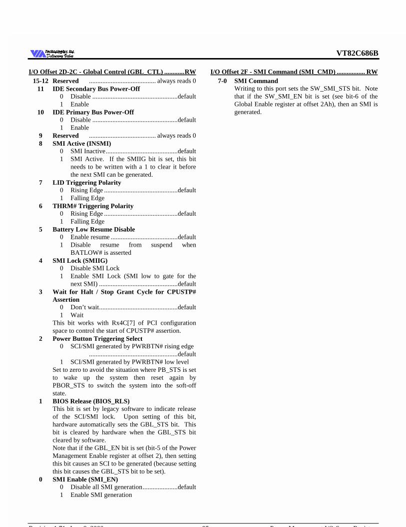
VT82C686B
Revision 1.71 June 9, 2000 -95- Power Management I/O-Space Registers
7HFKQRORJLHV ,QF'HOLYHULQJ 9DOXH'HOLYHULQJ 9DOXH
I/O Offset 2D-2C - Global Control (GBL_CTL) ............ RW15-12 Reserved ........................................ always reads 0
11 IDE Secondary Bus Power-Off0 Disable ...................................................default1 Enable
10 IDE Primary Bus Power-Off0 Disable ...................................................default1 Enable
9 Reserved ........................................ always reads 08 SMI Active (INSMI)
0 SMI Inactive...........................................default1 SMI Active. If the SMIIG bit is set, this bit
needs to be written with a 1 to clear it beforethe next SMI can be generated.
7 LID Triggering Polarity0 Rising Edge ............................................default1 Falling Edge
6 THRM# Triggering Polarity0 Rising Edge ............................................default1 Falling Edge
5 Battery Low Resume Disable0 Enable resume ........................................default1 Disable resume from suspend when
BATLOW# is asserted4 SMI Lock (SMIIG)
0 Disable SMI Lock1 Enable SMI Lock (SMI low to gate for the
next SMI) ...............................................default3 Wait for Halt / Stop Grant Cycle for CPUSTP#
Assertion0 Don’t wait...............................................default1 Wait
This bit works with Rx4C[7] of PCI configurationspace to control the start of CPUSTP# assertion.
2 Power Button Triggering Select0 SCI/SMI generated by PWRBTN# rising edge
.....................................................default1 SCI/SMI generated by PWRBTN# low level
Set to zero to avoid the situation where PB_STS is setto wake up the system then reset again byPBOR_STS to switch the system into the soft-offstate.
1 BIOS Release (BIOS_RLS)This bit is set by legacy software to indicate releaseof the SCI/SMI lock. Upon setting of this bit,hardware automatically sets the GBL_STS bit. Thisbit is cleared by hardware when the GBL_STS bitcleared by software.Note that if the GBL_EN bit is set (bit-5 of the PowerManagement Enable register at offset 2), then settingthis bit causes an SCI to be generated (because settingthis bit causes the GBL_STS bit to be set).
0 SMI Enable (SMI_EN)0 Disable all SMI generation.....................default1 Enable SMI generation
I/O Offset 2F - SMI Command (SMI_CMD) ................. RW7-0 SMI Command
Writing to this port sets the SW_SMI_STS bit. Notethat if the SW_SMI_EN bit is set (see bit-6 of theGlobal Enable register at offset 2Ah), then an SMI isgenerated.
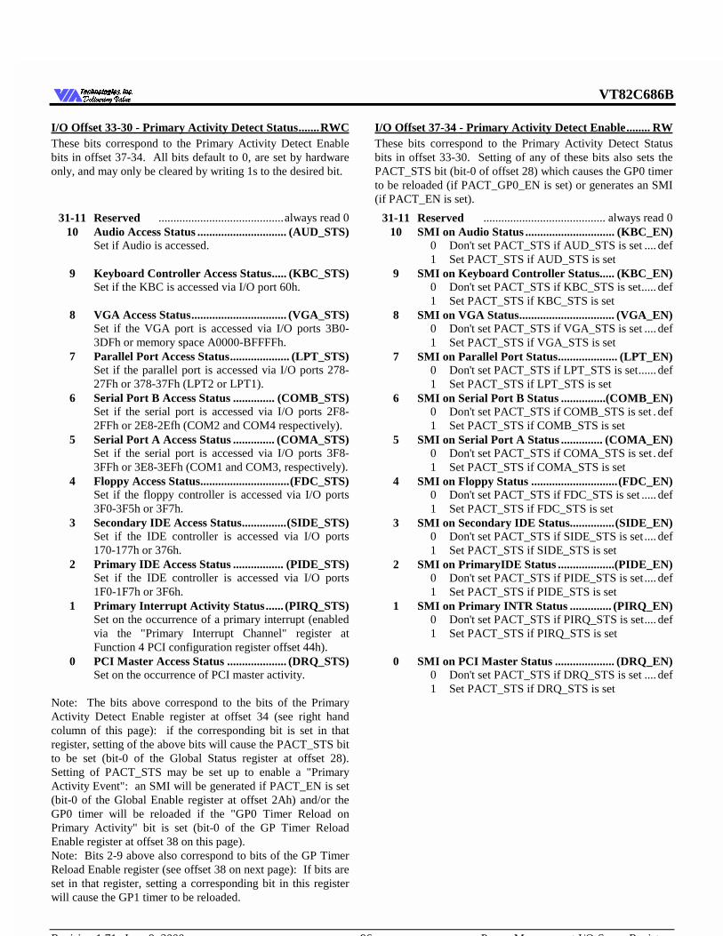
VT82C686B
Revision 1.71 June 9, 2000 -96- Power Management I/O-Space Registers
7HFKQRORJLHV ,QF'HOLYHULQJ 9DOXH'HOLYHULQJ 9DOXH
I/O Offset 33-30 - Primary Activity Detect Status ....... RWCThese bits correspond to the Primary Activity Detect Enablebits in offset 37-34. All bits default to 0, are set by hardwareonly, and may only be cleared by writing 1s to the desired bit.
31-11 Reserved ..........................................always read 010 Audio Access Status .............................. (AUD_STS)
Set if Audio is accessed.
9 Keyboard Controller Access Status..... (KBC_STS)Set if the KBC is accessed via I/O port 60h.
8 VGA Access Status................................ (VGA_STS)Set if the VGA port is accessed via I/O ports 3B0-3DFh or memory space A0000-BFFFFh.
7 Parallel Port Access Status.................... (LPT_STS)Set if the parallel port is accessed via I/O ports 278-27Fh or 378-37Fh (LPT2 or LPT1).
6 Serial Port B Access Status .............. (COMB_STS)Set if the serial port is accessed via I/O ports 2F8-2FFh or 2E8-2Efh (COM2 and COM4 respectively).
5 Serial Port A Access Status .............. (COMA_STS)Set if the serial port is accessed via I/O ports 3F8-3FFh or 3E8-3EFh (COM1 and COM3, respectively).
4 Floppy Access Status..............................(FDC_STS)Set if the floppy controller is accessed via I/O ports3F0-3F5h or 3F7h.
3 Secondary IDE Access Status...............(SIDE_STS)Set if the IDE controller is accessed via I/O ports170-177h or 376h.
2 Primary IDE Access Status ................. (PIDE_STS)Set if the IDE controller is accessed via I/O ports1F0-1F7h or 3F6h.
1 Primary Interrupt Activity Status...... (PIRQ_STS)Set on the occurrence of a primary interrupt (enabledvia the "Primary Interrupt Channel" register atFunction 4 PCI configuration register offset 44h).
0 PCI Master Access Status .................... (DRQ_STS)Set on the occurrence of PCI master activity.
Note: The bits above correspond to the bits of the PrimaryActivity Detect Enable register at offset 34 (see right handcolumn of this page): if the corresponding bit is set in thatregister, setting of the above bits will cause the PACT_STS bitto be set (bit-0 of the Global Status register at offset 28).Setting of PACT_STS may be set up to enable a "PrimaryActivity Event": an SMI will be generated if PACT_EN is set(bit-0 of the Global Enable register at offset 2Ah) and/or theGP0 timer will be reloaded if the "GP0 Timer Reload onPrimary Activity" bit is set (bit-0 of the GP Timer ReloadEnable register at offset 38 on this page).Note: Bits 2-9 above also correspond to bits of the GP TimerReload Enable register (see offset 38 on next page): If bits areset in that register, setting a corresponding bit in this registerwill cause the GP1 timer to be reloaded.
I/O Offset 37-34 - Primary Activity Detect Enable ........ RWThese bits correspond to the Primary Activity Detect Statusbits in offset 33-30. Setting of any of these bits also sets thePACT_STS bit (bit-0 of offset 28) which causes the GP0 timerto be reloaded (if PACT_GP0_EN is set) or generates an SMI(if PACT_EN is set).
31-11 Reserved ......................................... always read 010 SMI on Audio Status .............................. (KBC_EN)
0 Don't set PACT_STS if AUD_STS is set .... def1 Set PACT_STS if AUD_STS is set
9 SMI on Keyboard Controller Status..... (KBC_EN)0 Don't set PACT_STS if KBC_STS is set..... def1 Set PACT_STS if KBC_STS is set
8 SMI on VGA Status................................ (VGA_EN)0 Don't set PACT_STS if VGA_STS is set .... def1 Set PACT_STS if VGA_STS is set
7 SMI on Parallel Port Status.................... (LPT_EN)0 Don't set PACT_STS if LPT_STS is set...... def1 Set PACT_STS if LPT_STS is set
6 SMI on Serial Port B Status ...............(COMB_EN)0 Don't set PACT_STS if COMB_STS is set . def1 Set PACT_STS if COMB_STS is set
5 SMI on Serial Port A Status .............. (COMA_EN)0 Don't set PACT_STS if COMA_STS is set . def1 Set PACT_STS if COMA_STS is set
4 SMI on Floppy Status .............................(FDC_EN)0 Don't set PACT_STS if FDC_STS is set ..... def1 Set PACT_STS if FDC_STS is set
3 SMI on Secondary IDE Status...............(SIDE_EN)0 Don't set PACT_STS if SIDE_STS is set .... def1 Set PACT_STS if SIDE_STS is set
2 SMI on PrimaryIDE Status ...................(PIDE_EN)0 Don't set PACT_STS if PIDE_STS is set .... def1 Set PACT_STS if PIDE_STS is set
1 SMI on Primary INTR Status .............. (PIRQ_EN)0 Don't set PACT_STS if PIRQ_STS is set.... def1 Set PACT_STS if PIRQ_STS is set
0 SMI on PCI Master Status .................... (DRQ_EN)0 Don't set PACT_STS if DRQ_STS is set .... def1 Set PACT_STS if DRQ_STS is set
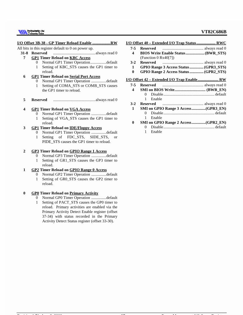
VT82C686B
Revision 1.71 June 9, 2000 -97- Power Management I/O-Space Registers
7HFKQRORJLHV ,QF'HOLYHULQJ 9DOXH'HOLYHULQJ 9DOXH
I/O Offset 3B-38 - GP Timer Reload Enable .................. RWAll bits in this register default to 0 on power up.
31-8 Reserved ..........................................always read 07 GP1 Timer Reload on KBC Access
0 Normal GP1 Timer Operation................default1 Setting of KBC_STS causes the GP1 timer to
reload.6 GP1 Timer Reload on Serial Port Access
0 Normal GP1 Timer Operation ...............default1 Setting of COMA_STS or COMB_STS causes
the GP1 timer to reload.
5 Reserved ..........................................always read 0
4 GP1 Timer Reload on VGA Access0 Normal GP1 Timer Operation ...............default1 Setting of VGA_STS causes the GP1 timer to
reload.3 GP1 Timer Reload on IDE/Floppy Access
0 Normal GP1 Timer Operation ...............default1 Setting of FDC_STS, SIDE_STS, or
PIDE_STS causes the GP1 timer to reload.
2 GP3 Timer Reload on GPIO Range 1 Access0 Normal GP3 Timer Operation ...............default1 Setting of GR1_STS causes the GP3 timer to
reload.1 GP2 Timer Reload on GPIO Range 0 Access
0 Normal GP2 Timer Operation ...............default1 Setting of GR0_STS causes the GP2 timer to
reload.
0 GP0 Timer Reload on Primary Activity0 Normal GP0 Timer Operation ...............default1 Setting of PACT_STS causes the GP0 timer to
reload. Primary activities are enabled via thePrimary Activity Detect Enable register (offset37-34) with status recorded in the PrimaryActivity Detect Status register (offset 33-30).
I/O Offset 40 – Extended I/O Trap Status ................... RWC7-5 Reserved ......................................... always read 04 BIOS Write Enable Status................... (BWR_STS)
(Function 0 Rx40[7])3-2 Reserved ......................................... always read 01 GPIO Range 3 Access Status .............. (GPR3_STS)0 GPIO Range 2 Access Status .............. (GPR2_STS)
I/O Offset 42 – Extended I/O Trap Enable ..................... RW7-5 Reserved ......................................... always read 04 SMI on BIOS Write............................... (BWR_EN)
0 Disable................................................... default1 Enable
3-2 Reserved ......................................... always read 01 SMI on GPIO Range 3 Access..............(GPR3_EN)
0 Disable................................................... default1 Enable
0 SMI on GPIO Range 2 Access..............(GPR2_EN)0 Disable................................................... default1 Enable
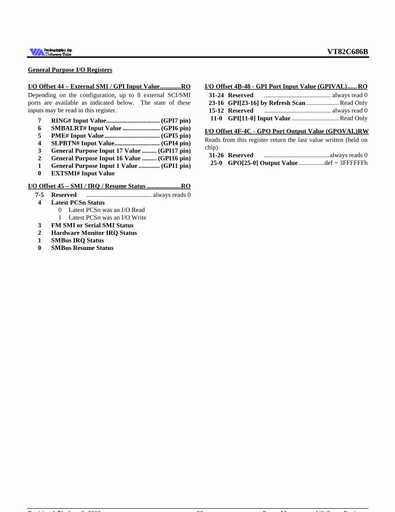
VT82C686B
Revision 1.71 June 9, 2000 -98- Power Management I/O-Space Registers
7HFKQRORJLHV ,QF'HOLYHULQJ 9DOXH'HOLYHULQJ 9DOXH
General Purpose I/O Registers
I/O Offset 44 – External SMI / GPI Input Value ............. RODepending on the configuration, up to 8 external SCI/SMIports are available as indicated below. The state of theseinputs may be read in this register.
7 RING# Input Value................................. (GPI7 pin)6 SMBALRT# Input Value ....................... (GPI6 pin)5 PME# Input Value .................................. (GPI5 pin)4 SLPBTN# Input Value............................ (GPI4 pin)3 General Purpose Input 17 Value ......... (GPI17 pin)2 General Purpose Input 16 Value ......... (GPI16 pin)1 General Purpose Input 1 Value ............. (GPI1 pin)0 EXTSMI# Input Value
I/O Offset 45 – SMI / IRQ / Resume Status ..................... RO7-5 Reserved ........................................ always reads 04 Latest PCSn Status
0 Latest PCSn was an I/O Read1 Latest PCSn was an I/O Write
3 FM SMI or Serial SMI Status2 Hardware Monitor IRQ Status1 SMBus IRQ Status0 SMBus Resume Status
I/O Offset 4B-48 - GPI Port Input Value (GPIVAL) ...... RO31-24 Reserved ......................................... always read 023-16 GPI[23-16] by Refresh Scan .................... Read Only15-12 Reserved ......................................... always read 011-0 GPI[11-0] Input Value ............................. Read Only
I/O Offset 4F-4C - GPO Port Output Value (GPOVAL) RWReads from this register return the last value written (held onchip)
31-26 Reserved ........................................always reads 025-0 GPO[25-0] Output Value ................def = 3FFFFFFh
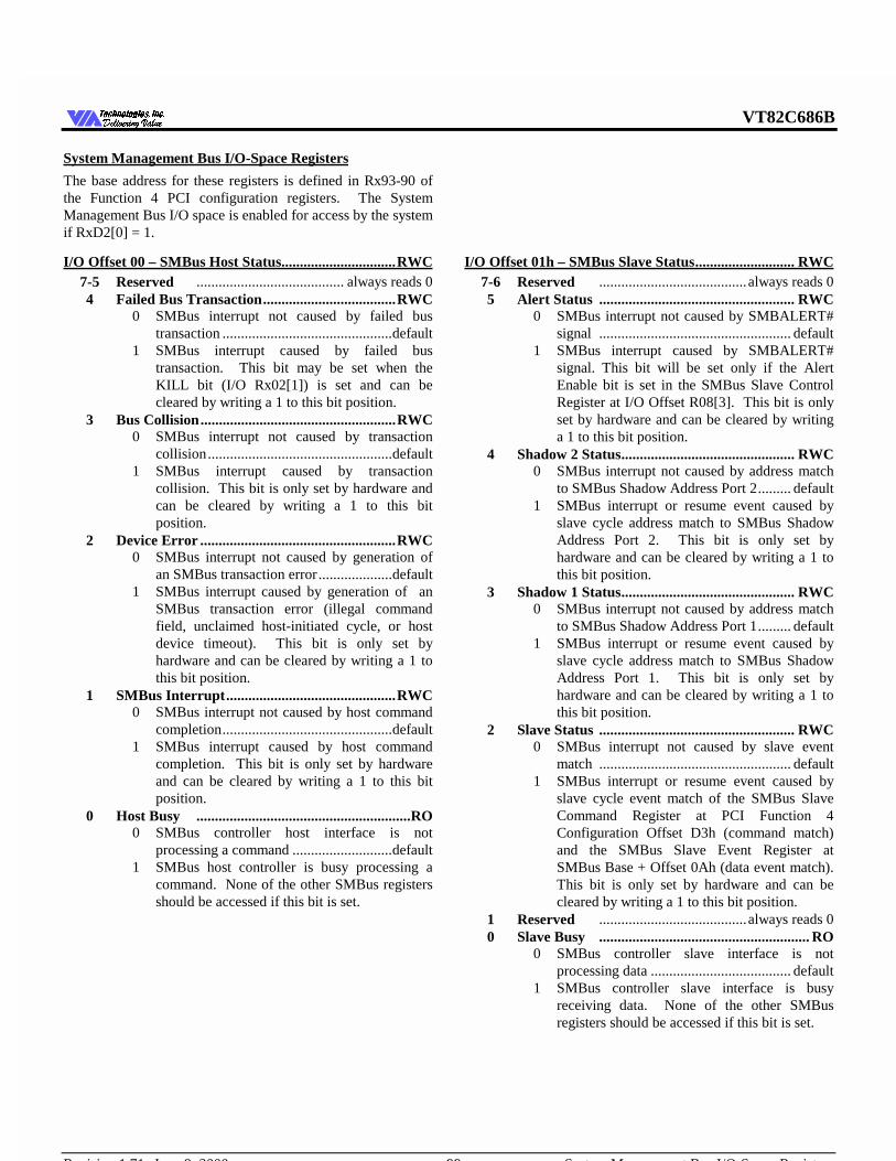
VT82C686B
Revision 1.71 June 9, 2000 -99- System Management Bus I/O-Space Registers
7HFKQRORJLHV ,QF'HOLYHULQJ 9DOXH'HOLYHULQJ 9DOXH
System Management Bus I/O-Space Registers
The base address for these registers is defined in Rx93-90 ofthe Function 4 PCI configuration registers. The SystemManagement Bus I/O space is enabled for access by the systemif RxD2[0] = 1.
I/O Offset 00 – SMBus Host Status............................... RWC7-5 Reserved ........................................ always reads 04 Failed Bus Transaction....................................RWC
0 SMBus interrupt not caused by failed bustransaction ..............................................default
1 SMBus interrupt caused by failed bustransaction. This bit may be set when theKILL bit (I/O Rx02[1]) is set and can becleared by writing a 1 to this bit position.
3 Bus Collision.....................................................RWC0 SMBus interrupt not caused by transaction
collision..................................................default1 SMBus interrupt caused by transaction
collision. This bit is only set by hardware andcan be cleared by writing a 1 to this bitposition.
2 Device Error .....................................................RWC0 SMBus interrupt not caused by generation of
an SMBus transaction error....................default1 SMBus interrupt caused by generation of an
SMBus transaction error (illegal commandfield, unclaimed host-initiated cycle, or hostdevice timeout). This bit is only set byhardware and can be cleared by writing a 1 tothis bit position.
1 SMBus Interrupt..............................................RWC0 SMBus interrupt not caused by host command
completion..............................................default1 SMBus interrupt caused by host command
completion. This bit is only set by hardwareand can be cleared by writing a 1 to this bitposition.
0 Host Busy ..........................................................RO0 SMBus controller host interface is not
processing a command ...........................default1 SMBus host controller is busy processing a
command. None of the other SMBus registersshould be accessed if this bit is set.
I/O Offset 01h – SMBus Slave Status ........................... RWC7-6 Reserved ........................................always reads 05 Alert Status ..................................................... RWC
0 SMBus interrupt not caused by SMBALERT#signal .................................................... default
1 SMBus interrupt caused by SMBALERT#signal. This bit will be set only if the AlertEnable bit is set in the SMBus Slave ControlRegister at I/O Offset R08[3]. This bit is onlyset by hardware and can be cleared by writinga 1 to this bit position.
4 Shadow 2 Status............................................... RWC0 SMBus interrupt not caused by address match
to SMBus Shadow Address Port 2......... default1 SMBus interrupt or resume event caused by
slave cycle address match to SMBus ShadowAddress Port 2. This bit is only set byhardware and can be cleared by writing a 1 tothis bit position.
3 Shadow 1 Status............................................... RWC0 SMBus interrupt not caused by address match
to SMBus Shadow Address Port 1......... default1 SMBus interrupt or resume event caused by
slave cycle address match to SMBus ShadowAddress Port 1. This bit is only set byhardware and can be cleared by writing a 1 tothis bit position.
2 Slave Status ..................................................... RWC0 SMBus interrupt not caused by slave event
match .................................................... default1 SMBus interrupt or resume event caused by
slave cycle event match of the SMBus SlaveCommand Register at PCI Function 4Configuration Offset D3h (command match)and the SMBus Slave Event Register atSMBus Base + Offset 0Ah (data event match).This bit is only set by hardware and can becleared by writing a 1 to this bit position.
1 Reserved ........................................always reads 00 Slave Busy ......................................................... RO
0 SMBus controller slave interface is notprocessing data ...................................... default
1 SMBus controller slave interface is busyreceiving data. None of the other SMBusregisters should be accessed if this bit is set.

VT82C686B
Revision 1.71 June 9, 2000 -100- System Management Bus I/O-Space Registers
7HFKQRORJLHV ,QF'HOLYHULQJ 9DOXH'HOLYHULQJ 9DOXH
I/O Offset 02h – SMBus Host Control ............................. RW7 Reserved ........................................ always reads 06 Start ........................................ always reads 0
0 Writing 0 has no effect ...........................default1 Start Execution of Command
Writing a 1 to this bit causes the SMBuscontroller host interface to initiate execution ofthe command programmed in the SMBusCommand Protocol field (bits 4-2). Allnecessary registers should be programmedprior to writing a 1 to this bit. The Host Busybit (SMBus Host Status Register bit-0) can beused to identify when the SMBus controllerhas completed command execution.
5-2 SMBus Command Protocol0000 Quick Read or Write ..............................default0001 Byte Read or Write0010 Byte Data Read or Write0011 Word Data Read or Write0100 Process Call0101 Block Read or Write0110 I2C with 10-bit Address0111 Reserved1000 -reserved-1001 -reserved-1010 -reserved-1011 -rreserved-1100 I2C Process Call1101 I2C Block1110 I2C with 7-bit Address1111 Universal
1 Kill Transaction in Progress0 Normal host controller operation ...........default1 Stop host transaction currently in progress.
Setting this bit also sets the FAILED status bit(Host Status bit-4) and asserts the interruptselected by the SMB Interrupt Select bit(Function 4 SMBus Host ConfigurationRegister RxD2[3]).
0 Interrupt Enable0 Disable interrupt generation ...................default1 Enable generation of interrupts on completion
of the current host transaction.
I/O Offset 03h – SMBus Host Command ........................ RW7-0 SMBUS Host Command ..........................default = 0
This field contains the data transmitted in thecommand field of the SMBus host transaction.
I/O Offset 04h – SMBus Host Address............................ RWThe contents of this register are transmitted in the address fieldof the SMBus host transaction.
7-1 SMBUS Address .......................................default = 0This field contains the 7-bit address of the targetedslave device.
0 SMBUS Read or Write0 Execute a WRITE command ................. default1 Execute a READ command
I/O Offset 05h – SMBus Host Data 0 .............................. RWThe contents of this register are transmitted in the Data 0 fieldof SMBus host transaction writes. On reads, Data 0 bytes arestored here.
7-0 SMBUS Data 0..........................................default = 0For Block Write commands, this field is programmedwith the block transfer count (a value between 1 and32). Counts of 0 or greater than 32 are undefined.For Block Read commands, the count received fromthe SMBus device is stored here.
I/O Offset 06h – SMBus Host Data 1 .............................. RWThe contents of this register are transmitted in the Data 1 fieldof SMBus host transaction writes. On reads, Data 1 bytes arestored here.
7-0 SMBUS Data 1..........................................default = 0
I/O Offset 07h – SMBus Block Data ............................... RWReads and writes to this register are used to access the 32-byteblock data storage array. An internal index pointer is used toaddress the array. It is reset to 0 by reads of the SMBus HostControl register (I/O Offset 2) and incremented automaticallyby each access to this register. The transfer of block data into(read) or out of (write) this storage array during an SMBustransaction always starts at index address 0.
7-0 SMBUS Block Data ..................................default = 0
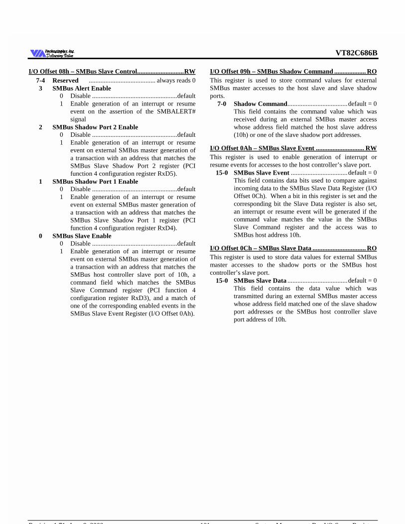
VT82C686B
Revision 1.71 June 9, 2000 -101- System Management Bus I/O-Space Registers
7HFKQRORJLHV ,QF'HOLYHULQJ 9DOXH'HOLYHULQJ 9DOXH
I/O Offset 08h – SMBus Slave Control ............................ RW7-4 Reserved ........................................ always reads 03 SMBus Alert Enable
0 Disable ...................................................default1 Enable generation of an interrupt or resume
event on the assertion of the SMBALERT#signal
2 SMBus Shadow Port 2 Enable0 Disable ...................................................default1 Enable generation of an interrupt or resume
event on external SMBus master generation ofa transaction with an address that matches theSMBus Slave Shadow Port 2 register (PCIfunction 4 configuration register RxD5).
1 SMBus Shadow Port 1 Enable0 Disable ...................................................default1 Enable generation of an interrupt or resume
event on external SMBus master generation ofa transaction with an address that matches theSMBus Slave Shadow Port 1 register (PCIfunction 4 configuration register RxD4).
0 SMBus Slave Enable0 Disable ...................................................default1 Enable generation of an interrupt or resume
event on external SMBus master generation ofa transaction with an address that matches theSMBus host controller slave port of 10h, acommand field which matches the SMBusSlave Command register (PCI function 4configuration register RxD3), and a match ofone of the corresponding enabled events in theSMBus Slave Event Register (I/O Offset 0Ah).
I/O Offset 09h – SMBus Shadow Command ................... ROThis register is used to store command values for externalSMBus master accesses to the host slave and slave shadowports.
7-0 Shadow Command....................................default = 0This field contains the command value which wasreceived during an external SMBus master accesswhose address field matched the host slave address(10h) or one of the slave shadow port addresses.
I/O Offset 0Ah – SMBus Slave Event ............................. RWThis register is used to enable generation of interrupt orresume events for accesses to the host controller’s slave port.
15-0 SMBus Slave Event ..................................default = 0This field contains data bits used to compare againstincoming data to the SMBus Slave Data Register (I/OOffset 0Ch). When a bit in this register is set and thecorresponding bit the Slave Data register is also set,an interrupt or resume event will be generated if thecommand value matches the value in the SMBusSlave Command register and the access was toSMBus host address 10h.
I/O Offset 0Ch – SMBus Slave Data ................................ ROThis register is used to store data values for external SMBusmaster accesses to the shadow ports or the SMBus hostcontroller’s slave port.
15-0 SMBus Slave Data ....................................default = 0This field contains the data value which wastransmitted during an external SMBus master accesswhose address field matched one of the slave shadowport addresses or the SMBus host controller slaveport address of 10h.

VT82C686B
Revision 1.71 June 9, 2000 -102- Hardware Monitor I/O Space Registers
7HFKQRORJLHV ,QF'HOLYHULQJ 9DOXH'HOLYHULQJ 9DOXH
Hardware Monitor I/O Space Registers
The I/O base address for access to the Hardware Monitorregisters is defined in Rx71-70 of function 4 PCI configurationspace. The hardware monitor I/O space is enabled for I/Oaccess by the system if Rx74[0] = 1.
Offset 13 – Analog Data 15-8 ........................................... RW
Offset 14 – Analog Data 7-0 ............................................. RW
Offset 15 – Digital Data 7-0 .............................................. RW
Offset 16 – Channel Counter ............................................ RW
Offset 17 – Data Valid & Channel Indicators ................. RW
Offset 1D – TSENS3 Hot Temperature High Limit ....... RW
Offset 1E – TSENS3 Hot Temp Hysteresis Lo Limit...... RW
Offset 1F – TSENS3 Temperature Reading .................... RWTemperature sensor 3 is an internal bandgap-type sensor whichhas 10-bit resolution. The high order 8 bits are stored here andthe low order 2 bits are stored in Rx49[7-6]. Only the highorder 8 bits are used for comparison with the limit values inoffsets 1D and 1E.
Offset 20 – TSENS1 Temperature Reading .................... RWTemperature sensor 1 is an external sensor input on pin W13which has 10-bit resolution. The high order 8 bits are storedhere and the low order 2 bits are stored in Rx4B[7-6]. Onlythe high order 8 bits are used for comparison with the limitvalues in offsets 39 and 3A.
Offset 21 – TSENS2 Temperature Reading .................... RWTemperature sensor 2 is an external sensor input on pin Y13which has 10-bit resolution. The high order 8 bits are storedhere and the low order 2 bits are stored in Rx49[5-4]. Onlythe high order 8 bits are used for comparison with the limitvalues in offsets 3D and 3E.
Offset 22 – VSENS1 (Pin U13) Voltage Reading (2.0V). RW
Offset 23 – VSENS2 (Pin V13) Voltage Reading (2.5V). RW
Offset 24 – Internal Core Voltage Reading (3.3V) ......... RW
Offset 25 – VSENS3 (Pin W14) Voltage Reading (5V) .. RW
Offset 26 – VSENS4 (Pin Y14) Voltage Reading (12V).. RW
Offset 27 – Reserved (-12V Sense Voltage Reading) ...... RW
Offset 28 – Reserved (-5V Sense Voltage Reading) ........ RW
Offset 29 – FAN1 (Pin T12) Count Reading ................... RWOffset 2A – FAN2 (Pin U12) Count Reading .................. RWThe above two locations store the number of counts of theinternal clock per fan revolution.
Offset 2B – VSENS1 Voltage High Limit (CPU 2.0V) ... RW
Offset 2C – VSENS1 Voltage Low Limit (CPU 2.0V) ... RW
Offset 2D – VSENS2 Voltage High Limit (NB 2.5V) ..... RW
Offset 2E – VSENS2 Voltage Low Limit (NB 2.5V) ...... RW
Offset 2F – Internal Core Voltage High Limit (3.3V) .... RW
Offset 30 – Internal Core Voltage Low Limit (3.3V) ..... RW
Offset 31 – VSENS3 Voltage High Limit (5V) ................ RW
Offset 32 – VSENS3 Voltage Low Limit (5V) ................ RW
Offset 33 – VSENS4 Voltage High Limit (12V) .............. RW
Offset 34 – VSENS4 Voltage Low Limit (12V) .............. RW
Offset 35 – Reserved (-12V Sense High Limit) ............... RW
Offset 36 – Reserved (-12V Sense Low Limit) ................ RW
Offset 37 – Reserved (-5V Sense High Limit) ................. RW
Offset 38 – Reserved (-5V Sense Low Limit) .................. RW
Offset 39 – TSENS1 Hot Temperature High Limit ........ RW
Offset 3A – TSENS1Hot Temp Hysteresis Lo Limit ...... RW
Offset 3B – FAN1 Fan Count Limit ................................ RW
Offset 3C – FAN2 Fan Count Limit ................................ RWThe above two locations store the number of counts of theinternal clock per fan revolution for the low limit of the fanspeed.
Offset 3D – TSENS2 Hot Temperature High Limit ....... RW
Offset 3E – TSENS2 Hot Temp Hysteresis Lo Limit ..... RW
Offset 3F – Stepping ID Number ..................................... RW
Note: For high limits, comparisons are “greater than”comparisons. For low limits, comparisons are “less than orequal” comparisons.
One consequence of the above is that if high limits are set toall ones (FFh or 11111111b), interrupts are disabled for highlimits (i.e., interrupts will only be generated for cases whenvoltages are equal to or below the low limits).
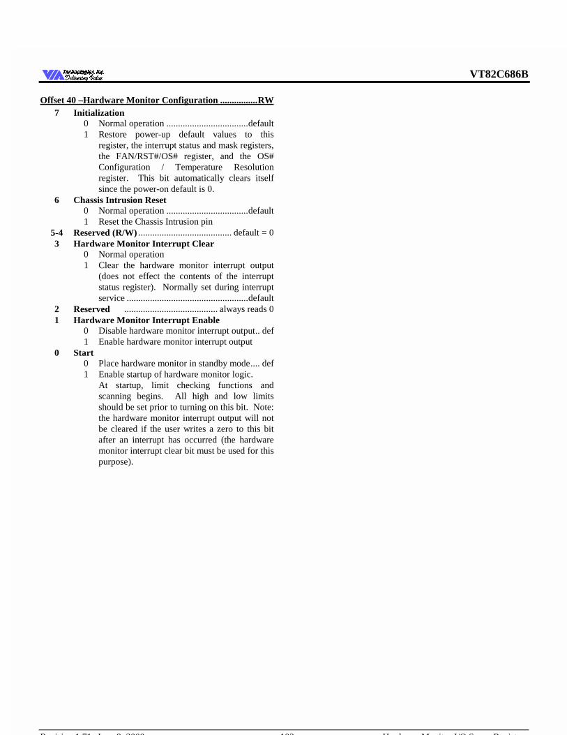
VT82C686B
Revision 1.71 June 9, 2000 -103- Hardware Monitor I/O Space Registers
7HFKQRORJLHV ,QF'HOLYHULQJ 9DOXH'HOLYHULQJ 9DOXH
Offset 40 –Hardware Monitor Configuration ................ RW7 Initialization
0 Normal operation ...................................default1 Restore power-up default values to this
register, the interrupt status and mask registers,the FAN/RST#/OS# register, and the OS#Configuration / Temperature Resolutionregister. This bit automatically clears itselfsince the power-on default is 0.
6 Chassis Intrusion Reset0 Normal operation ...................................default1 Reset the Chassis Intrusion pin
5-4 Reserved (R/W) ........................................ default = 03 Hardware Monitor Interrupt Clear
0 Normal operation1 Clear the hardware monitor interrupt output
(does not effect the contents of the interruptstatus register). Normally set during interruptservice ....................................................default
2 Reserved ........................................ always reads 01 Hardware Monitor Interrupt Enable
0 Disable hardware monitor interrupt output.. def1 Enable hardware monitor interrupt output
0 Start0 Place hardware monitor in standby mode.... def1 Enable startup of hardware monitor logic.
At startup, limit checking functions andscanning begins. All high and low limitsshould be set prior to turning on this bit. Note:the hardware monitor interrupt output will notbe cleared if the user writes a zero to this bitafter an interrupt has occurred (the hardwaremonitor interrupt clear bit must be used for thispurpose).

VT82C686B
Revision 1.71 June 9, 2000 -104- Hardware Monitor I/O Space Registers
7HFKQRORJLHV ,QF'HOLYHULQJ 9DOXH'HOLYHULQJ 9DOXH
Offset 41 –Hardware Monitor Interrupt Status 1 ........... RO7 Fan 2 Error
0 No error ..................................................default1 Fan 2 count limit exceeded
6 Fan 1 Error0 No error ..................................................default1 Fan 1 count limit exceeded
5 Reserved ........................................ always reads 0
4 TSENS1 Temperature Error0 No error ..................................................default1 High or low hot temperature limit exceeded.
The interrupt mode is determined byTemperature Resolution register Rx4B[1-0].
3 VSENS3 Voltage Error (5V)0 No error ..................................................default1 High or low limit exceeded
2 Internal Core VCC Voltage Error (3.3V)0 No error ..................................................default1 High or low limit exceeded
1 VSENS2 Voltage Error (2.5V NB Core Voltage)0 No error ..................................................default1 High or low limit exceeded
0 VSENS1 Voltage Error (2.0V CPU Core Voltage)0 No error ..................................................default1 High or low limit exceeded
Offset 42 –Hardware Monitor Interrupt Status 2 ........... RO7 TSENS3 (Internal Bandgap) Temp Error
0 No error ..................................................default1 High or low hot temperature limit exceeded.
Interrupt mode is determined by Rx4B[5-4].6-5 Reserved ........................................ always reads 04 Chassis Error
0 No error ..................................................default1 Chassis Intrusion has gone high
3 TSENS2 Temperature Error0 No error ..................................................default1 High or low hot temperature limit exceeded.
Interrupt mode is determined by Rx4B[3-2].2-1 Reserved ........................................ always reads 00 VSENS4 Voltage Error (12V)
0 No error ..................................................default1 High or low limit exceeded
Note: When either status register is read, status conditions inthat register are reset. In the case of voltage priorityindications, if two or more voltages were out of limits, thenanother indication would automatically be generated if it wasnot handled during interrupt service. Errant voltages may bedisabled in the control register until the operator has time toclear the errant condition or set the limit higher or lower.
Offset 43 –Hardware Monitor Interrupt Mask 1 .......... RW7 Fan 2 Count Error Mask
0 Enable interrupt on error status bit set ......... def1 Disable interrupt on error status bit set
6 Fan 1 Count Error Mask0 Enable interrupt on error status bit set ......... def1 Disable interrupt on error status bit set
5 TSENS1 Thermal Alarm Control Mask0 Enable TSENS1 over-temp condition to
control the thermal alarm (function 4 Rx40[7]automatic CPU clock throttling must be set )def
1 Disable4 TSENS1 Temperature Error Mask
0 Enable interrupt on error status bit set ......... def1 Disable interrupt on error status bit set
3 VSENS3 Voltage Error Mask (5V)0 Enable interrupt on error status bit set ......... def1 Disable interrupt on error status bit set
2 Internal Core VCC Voltage Error Mask (3.3V)0 Enable interrupt on error status bit set ......... def1 Disable interrupt on error status bit set
1 VSENS2 Voltage Error Mask (2.5V NB Core)0 Enable interrupt on error status bit set ......... def1 Disable interrupt on error status bit set
0 VSENS1 Voltage Error Mask (2.0V CPU Core)0 Enable interrupt on error status bit set ......... def1 Disable interrupt on error status bit set
Offset 44 –Hardware Monitor Interrupt Mask 2 .......... RW7 TSENS3 Temperature Error Mask
0 Enable interrupt on error status bit set ......... def1 Disable interrupt on error status bit set
6 TSENS3 Thermal Alarm Control Mask0 Enable TSENS3 over-temp condition to
control the thermal alarm (function 4 Rx40[7]automatic CPU clock throttling must be set) def
1 Disable5 TSENS2 Thermal Alarm Control Mask
0 Enable TSENS2 over-temp condition tocontrol the thermal alarm (function 4 Rx40[7]automatic CPU clock throttling must be set)def
1 Disable4 Chassis Error Mask
0 Enable interrupt on error status bit set ......... def1 Disable interrupt on error status bit set
3 TSENS2 Temperature Error Mask0 Enable interrupt on error status bit set ......... def1 Disable interrupt on error status bit set
2-1 Reserved ........................................always reads 00 VSENS4 Voltage Error Mask (12V)
0 Enable interrupt on error status bit set ......... def1 Disable interrupt on error status bit set
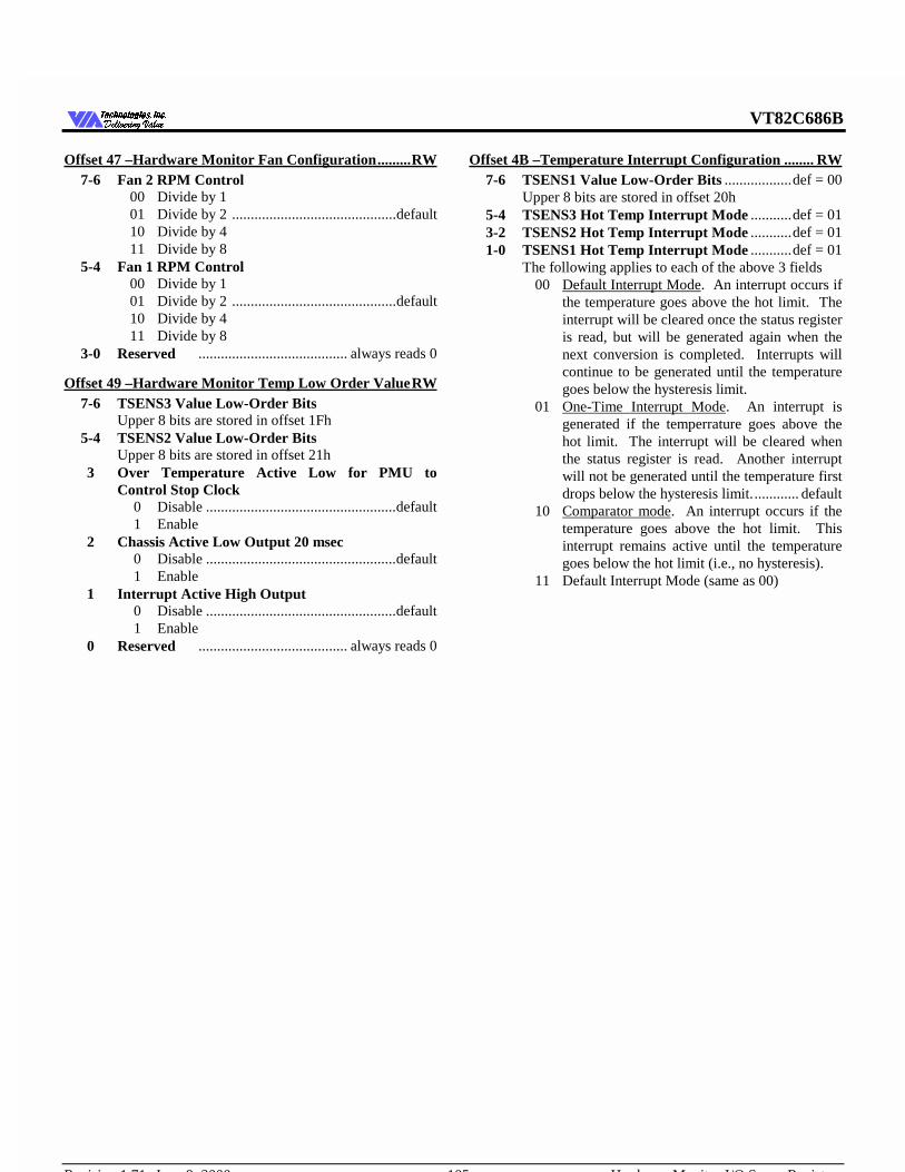
VT82C686B
Revision 1.71 June 9, 2000 -105- Hardware Monitor I/O Space Registers
7HFKQRORJLHV ,QF'HOLYHULQJ 9DOXH'HOLYHULQJ 9DOXH
Offset 47 –Hardware Monitor Fan Configuration ......... RW7-6 Fan 2 RPM Control
00 Divide by 101 Divide by 2 ............................................default10 Divide by 411 Divide by 8
5-4 Fan 1 RPM Control00 Divide by 101 Divide by 2 ............................................default10 Divide by 411 Divide by 8
3-0 Reserved ........................................ always reads 0
Offset 49 –Hardware Monitor Temp Low Order Value RW7-6 TSENS3 Value Low-Order Bits
Upper 8 bits are stored in offset 1Fh5-4 TSENS2 Value Low-Order Bits
Upper 8 bits are stored in offset 21h3 Over Temperature Active Low for PMU to
Control Stop Clock0 Disable ...................................................default1 Enable
2 Chassis Active Low Output 20 msec0 Disable ...................................................default1 Enable
1 Interrupt Active High Output0 Disable ...................................................default1 Enable
0 Reserved ........................................ always reads 0
Offset 4B –Temperature Interrupt Configuration ........ RW7-6 TSENS1 Value Low-Order Bits ..................def = 00
Upper 8 bits are stored in offset 20h5-4 TSENS3 Hot Temp Interrupt Mode ...........def = 013-2 TSENS2 Hot Temp Interrupt Mode ...........def = 011-0 TSENS1 Hot Temp Interrupt Mode ...........def = 01
The following applies to each of the above 3 fields00 Default Interrupt Mode. An interrupt occurs if
the temperature goes above the hot limit. Theinterrupt will be cleared once the status registeris read, but will be generated again when thenext conversion is completed. Interrupts willcontinue to be generated until the temperaturegoes below the hysteresis limit.
01 One-Time Interrupt Mode. An interrupt isgenerated if the temperrature goes above thehot limit. The interrupt will be cleared whenthe status register is read. Another interruptwill not be generated until the temperature firstdrops below the hysteresis limit............. default
10 Comparator mode. An interrupt occurs if thetemperature goes above the hot limit. Thisinterrupt remains active until the temperaturegoes below the hot limit (i.e., no hysteresis).
11 Default Interrupt Mode (same as 00)
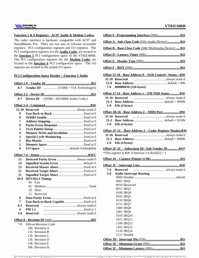
VT82C686B
Revision 1.71 June 9, 2000 -106- Function 5 & 6 Registers - AC97 Audio & Modem Codecs
7HFKQRORJLHV ,QF'HOLYHULQJ 9DOXH'HOLYHULQJ 9DOXH
Function 5 & 6 Registers - AC97 Audio & Modem Codecs
The codec interface is hardware compatible with AC97 andSoundBlaster Pro. There are two sets of software accessibleregisters: PCI configuration registers and I/O registers. ThePCI configuration registers for the Audio Codec are located inthe function 5 PCI configuration space of the VT82C686B.The PCI configuration registers for the Modem Codec arelocated in the function 6 PCI configuration space. The I/Oregisters are located in the system I/O space.
PCI Configuration Space Header – Function 5 Audio
Offset 1-0 - Vendor ID ....................................................... RO0-7 Vendor ID ................. (1106h = VIA Technologies)
Offset 3-2 - Device ID ......................................................... RO0-7 Device ID (3058h = 82C686B Audio Codec)
Offset 5-4 - Command ....................................................... RW15-10 Reserved ........................................ always reads 0
9 Fast Back-to-Back.......................................fixed at 08 SERR# Enable .............................................fixed at 07 Address Stepping ........................................fixed at 06 Parity Error Response ................................fixed at 05 VGA Palette Snoop .....................................fixed at 04 Memory Write and Invalidate ...................fixed at 03 Special Cycle Monitoring ...........................fixed at 02 Bus Master .................................................fixed at 01 Memory Space .............................................fixed at 00 I/O Space ............................... default=0 (disabled)
Offset 7-6 - Status ........................................................... RWC15 Detected Parity Error ........................ always reads 014 Signalled System Error.............................. default=013 Received Master Abort...............................fixed at 012 Received Target Abort ...............................fixed at 011 Signalled Target Abort ...............................fixed at 0
10-9 DEVSEL# Timing00 Fast01 Medium .................................................... fixed10 Slow11 Reserved
8 Data Parity Error........................................fixed at 07 Fast Back-to-Back Capable........................fixed at 0
6-5 Reserved ........................................ always reads 04 PM 1.1 .................................................fixed at 1
3-0 Reserved ........................................ always reads 0
Offset 8 - Revision ID (nnh) ............................................... RO7-0 Silicon Revision Code
10h Revision A11h Revision B12h Revision C13h Revision D14h Revision E20h Revision H
Offset 9 - Programming Interface (00h) ........................... RO
Offset A - Sub Class Code (01h=Audio Device) ............... RO
Offset B - Base Class Code (04h=Multimedia Device) ..... RO
Offset D - Latency Timer (00h) ......................................... RO
Offset E - Header Type (00h) ............................................ RO
Offset F - BIST (00h) ......................................................... RO
Offset 13-10 - Base Address 0 – SGD Control / Status .. RW31-16 Reserved ........................................always reads 015-8 Base Address .........................................default = 00h7-0 00000001b (256 bytes)
Offset 17-14 - Base Address 1 – FM NMI Status ........... RW31-16 Reserved ........................................always reads 015-2 Base Address .....................................default = 0000h1-0 01b (4 bytes)
Offset 1B-18 - Base Address 2 – MIDI Port ................... RW31-16 Reserved ........................................always reads 015-2 Base Address .....................................default = 0330h1-0 01b (4 bytes)
Offset 1F-1C - Base Address 3 – Codec Register Shadow RW31-16 Reserved ........................................always reads 015-2 Base Address .....................................default = 0000h1-0 01b (4 bytes)
Offset 2F-2C – Subsystem ID / Sub Vendor ID ............. RO**This register is RW if function 5-6 Rx42[5] = 1
Offset 34 – Capture Pointer (C0h) ................................... RO
Offset 3C - Interrupt Line ................................................ RW7-4 Reserved ........................................always reads 03-0 Audio Interrupt Routing
0000 Disable................................................... default0001 IRQ10010 Reserved0011 IRQ30100 IRQ40101 IRQ50110 IRQ60111 IRQ71000 IRQ81001 IRQ91010 IRQ101011 IRQ111100 IRQ121101 IRQ131110 IRQ141111 Disable
Offset 3D - Interrupt Pin (03h) ......................................... ROOffset 3E - Minimum Grant (00h) .................................... ROOffset 3F - Minimum Latency (00h) ................................. RO
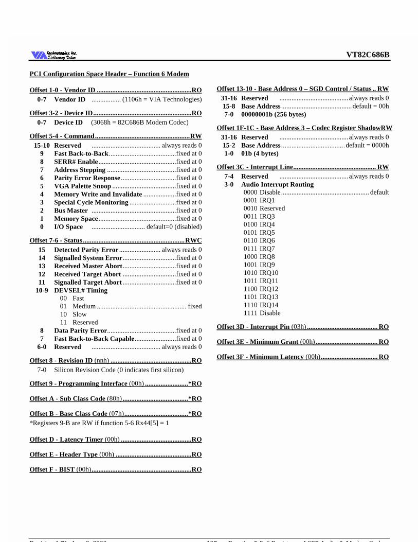
VT82C686B
Revision 1.71 June 9, 2000 -107- Function 5 & 6 Registers - AC97 Audio & Modem Codecs
7HFKQRORJLHV ,QF'HOLYHULQJ 9DOXH'HOLYHULQJ 9DOXH
PCI Configuration Space Header – Function 6 Modem
Offset 1-0 - Vendor ID ....................................................... RO0-7 Vendor ID ................. (1106h = VIA Technologies)
Offset 3-2 - Device ID ......................................................... RO0-7 Device ID (3068h = 82C686B Modem Codec)
Offset 5-4 - Command ....................................................... RW15-10 Reserved ........................................ always reads 0
9 Fast Back-to-Back.......................................fixed at 08 SERR# Enable .............................................fixed at 07 Address Stepping ........................................fixed at 06 Parity Error Response ................................fixed at 05 VGA Palette Snoop .....................................fixed at 04 Memory Write and Invalidate ...................fixed at 03 Special Cycle Monitoring ...........................fixed at 02 Bus Master .................................................fixed at 01 Memory Space .............................................fixed at 00 I/O Space ............................... default=0 (disabled)
Offset 7-6 - Status ........................................................... RWC15 Detected Parity Error ........................ always reads 014 Signalled System Error...............................fixed at 013 Received Master Abort...............................fixed at 012 Received Target Abort ...............................fixed at 011 Signalled Target Abort ...............................fixed at 0
10-9 DEVSEL# Timing00 Fast01 Medium .................................................... fixed10 Slow11 Reserved
8 Data Parity Error........................................fixed at 07 Fast Back-to-Back Capable........................fixed at 0
6-0 Reserved ........................................ always reads 0
Offset 8 - Revision ID (nnh) ............................................... RO7-0 Silicon Revision Code (0 indicates first silicon)
Offset 9 - Programming Interface (00h) ......................... *RO
Offset A - Sub Class Code (80h) ...................................... *RO
Offset B - Base Class Code (07h) ..................................... *RO*Registers 9-B are RW if function 5-6 Rx44[5] = 1
Offset D - Latency Timer (00h) ......................................... RO
Offset E - Header Type (00h) ............................................ RO
Offset F - BIST (00h) .......................................................... RO
Offset 13-10 - Base Address 0 – SGD Control / Status .. RW31-16 Reserved ........................................always reads 015-8 Base Address .........................................default = 00h7-0 00000001b (256 bytes)
Offset 1F-1C - Base Address 3 – Codec Register Shadow RW31-16 Reserved ........................................always reads 015-2 Base Address .....................................default = 0000h1-0 01b (4 bytes)
Offset 3C - Interrupt Line ................................................ RW7-4 Reserved ........................................always reads 03-0 Audio Interrupt Routing
0000 Disable................................................... default0001 IRQ10010 Reserved0011 IRQ30100 IRQ40101 IRQ50110 IRQ60111 IRQ71000 IRQ81001 IRQ91010 IRQ101011 IRQ111100 IRQ121101 IRQ131110 IRQ141111 Disable
Offset 3D - Interrupt Pin (03h) ......................................... RO
Offset 3E - Minimum Grant (00h) .................................... RO
Offset 3F - Minimum Latency (00h) ................................. RO
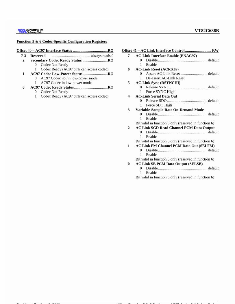
VT82C686B
Revision 1.71 June 9, 2000 -108- Function 5 & 6 Registers - AC97 Audio & Modem Codecs
7HFKQRORJLHV ,QF'HOLYHULQJ 9DOXH'HOLYHULQJ 9DOXH
Function 5 & 6 Codec-Specific Configuration Registers
Offset 40 – AC97 Interface Status .................................... RO7-3 Reserved ........................................ always reads 02 Secondary Codec Ready Status ..........................RO
0 Codec Not Ready1 Codec Ready (AC97 ctrlr can access codec)
1 AC97 Codec Low-Power Status..........................RO0 AC97 Codec not in low-power mode1 AC97 Codec in low-power mode
0 AC97 Codec Ready Status...................................RO0 Codec Not Ready1 Codec Ready (AC97 ctrlr can access codec)
Offset 41 – AC Link Interface Control ........................... RW7 AC-Link Interface Enable (ENAC97)
0 Disable................................................... default1 Enable
6 AC-Link Reset (ACRST#)0 Assert AC-Link Reset ............................ default1 De-assert AC-Link Reset
5 AC-Link Sync (RSYNCHI)0 Release SYNC ....................................... default1 Force SYNC High
4 AC-Link Serial Data Out0 Release SDO.......................................... default1 Force SDO High
3 Variable-Sample-Rate On-Demand Mode0 Disable................................................... default1 Enable
Bit valid in function 5 only (reserved in function 6)2 AC Link SGD Read Channel PCM Data Output
0 Disable................................................... default1 Enable
Bit valid in function 5 only (reserved in function 6)1 AC Link FM Channel PCM Data Out (SELFM)
0 Disable................................................... default1 Enable
Bit valid in function 5 only (reserved in function 6)0 AC Link SB PCM Data Output (SELSB)
0 Disable................................................... default1 Enable
Bit valid in function 5 only (reserved in function 6)

VT82C686B
Revision 1.71 June 9, 2000 -109- Function 5 & 6 Registers - AC97 Audio & Modem Codecs
7HFKQRORJLHV ,QF'HOLYHULQJ 9DOXH'HOLYHULQJ 9DOXH
Offset 42 – Function Enable ....................... RW (Function 5)Offset 42 – Function Enable ........................ RO (Function 6)
7 MIDI PnP0 MIDI Port Address Selected by Rx43[3-2] . def1 MIDI Port Address Selected by IOBase2
6 Mask MIDI IRQ0 Disable ...................................................default1 Enable
5 Function 5 Config Reg Rx2C Writable0 F5Rx2C-2F RO ......................................default1 F5Rx2C-2F RW
4 Gate SoundBlaster PCM When FIFO Empty0 Disable ...................................................default1 Enable
3 Game Port Enable (ENGAME)0 Disable ...................................................default1 Enable (200-207h)
2 FM Enable (ENFM)0 Disable ...................................................default1 Enable (388-38B)
1 MIDI Enable (ENMIDI)0 Disable ...................................................default1 Enable
0 SoundBlaster Enable (ENSB)0 Disable ...................................................default1 Enable
Offset 43 – Plug and Play Control ............. RW (Function 5)Offset 43 – Plug and Play Control .............. RO (Function 6)
7-6 SoundBlaster IRQ Select (SBIRQS[1:0])00 IRQ5 .....................................................default01 IRQ710 IRQ911 IRQ10
5-4 SoundBlaster DRQ Select (SBDRQS[1:0])00 DMA Channel 001 DMA Channel 1 .....................................default10 DMA Channel 211 DMA Channel 3
3-2 MIDI Decode Select (MIDIBASE)00 300-303h01 310-313h10 320-323h11 330-333h ................................................default
1-0 SoundBlaster Decode Select (SBBASE)00 220-22Fh ................................................default01 240-24Fh10 260-26Fh11 280-28Fh
Offset 44 – MC97 Interface Control .......... RO (Function 5)Offset 44 – MC97 Interface Control ......... RW (Function 6)
7 AC-Link Interface for Slot-50 Disable................................................... default1 Enable
6 Secondary Codec Support0 Disable................................................... default1 Enable
5 Function 6 Config Reg Rx9-B Writable0 F6Rx9-B RO.......................................... default1 F6Rx9-B RW
4 Function 6 Config Reg 2Ch Writable0 F6Rx2C-2F RO...................................... default1 F6Rx2C-2F RW
3-0 Reserved ........................................always reads 0
Offset 48 – FM NMI Control ..................... RW (Function 5)Offset 48 – FM NMI Control ...................... RO (Function 6)
7-3 Reserved ........................................always reads 02 FM IRQ Select
0 Route FM Trap interrupt to NMI........... default1 Route FM Trap interrupt to SMI
1 FM SGD Data for SoundBlaster Mixing0 Disable................................................... default1 Enable
0 FM Trap Interrupt0 Enable1 Disable .................................................. default
Offset 4B-4A – Game Port Base Address ....................... RW15-0 Game Port Base Address .........................default = 0
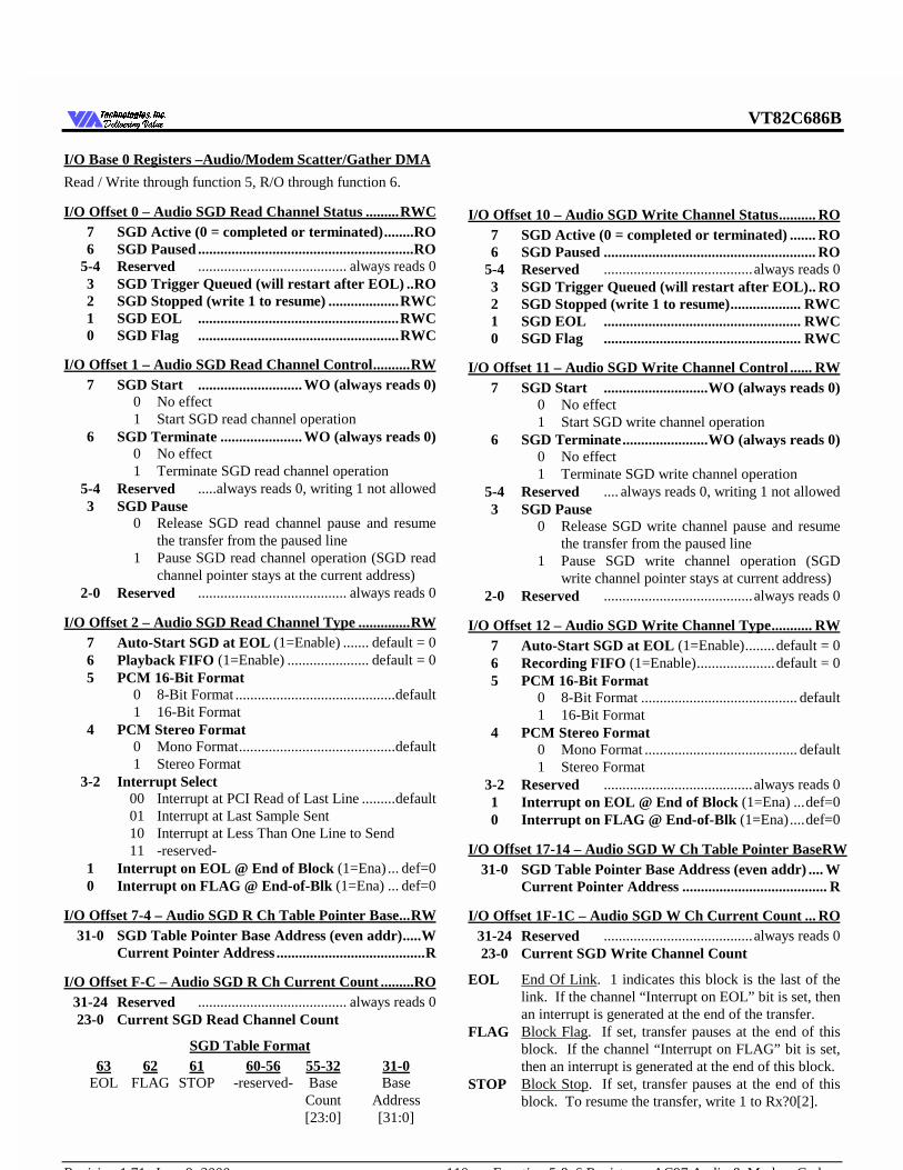
VT82C686B
Revision 1.71 June 9, 2000 -110- Function 5 & 6 Registers - AC97 Audio & Modem Codecs
7HFKQRORJLHV ,QF'HOLYHULQJ 9DOXH'HOLYHULQJ 9DOXH
I/O Base 0 Registers –Audio/Modem Scatter/Gather DMA
Read / Write through function 5, R/O through function 6.
I/O Offset 0 – Audio SGD Read Channel Status ......... RWC7 SGD Active (0 = completed or terminated)........RO6 SGD Paused ..........................................................RO
5-4 Reserved ........................................ always reads 03 SGD Trigger Queued (will restart after EOL) ..RO2 SGD Stopped (write 1 to resume) ...................RWC1 SGD EOL ......................................................RWC0 SGD Flag ......................................................RWC
I/O Offset 1 – Audio SGD Read Channel Control .......... RW7 SGD Start ............................ WO (always reads 0)
0 No effect1 Start SGD read channel operation
6 SGD Terminate ...................... WO (always reads 0)0 No effect1 Terminate SGD read channel operation
5-4 Reserved .....always reads 0, writing 1 not allowed3 SGD Pause
0 Release SGD read channel pause and resumethe transfer from the paused line
1 Pause SGD read channel operation (SGD readchannel pointer stays at the current address)
2-0 Reserved ........................................ always reads 0
I/O Offset 2 – Audio SGD Read Channel Type .............. RW7 Auto-Start SGD at EOL (1=Enable) ....... default = 06 Playback FIFO (1=Enable) ...................... default = 05 PCM 16-Bit Format
0 8-Bit Format ...........................................default1 16-Bit Format
4 PCM Stereo Format0 Mono Format..........................................default1 Stereo Format
3-2 Interrupt Select00 Interrupt at PCI Read of Last Line .........default01 Interrupt at Last Sample Sent10 Interrupt at Less Than One Line to Send11 -reserved-
1 Interrupt on EOL @ End of Block (1=Ena) ... def=00 Interrupt on FLAG @ End-of-Blk (1=Ena) ... def=0
I/O Offset 7-4 – Audio SGD R Ch Table Pointer Base ... RW31-0 SGD Table Pointer Base Address (even addr).....W
Current Pointer Address ........................................R
I/O Offset F-C – Audio SGD R Ch Current Count ......... RO31-24 Reserved ........................................ always reads 023-0 Current SGD Read Channel Count
SGD Table Format63 62 61 60-56 55-32 31-0
EOL FLAG STOP -reserved- Base BaseCount Address[23:0] [31:0]
I/O Offset 10 – Audio SGD Write Channel Status .......... RO7 SGD Active (0 = completed or terminated) ....... RO6 SGD Paused ......................................................... RO
5-4 Reserved ........................................always reads 03 SGD Trigger Queued (will restart after EOL).. RO2 SGD Stopped (write 1 to resume)................... RWC1 SGD EOL ..................................................... RWC0 SGD Flag ..................................................... RWC
I/O Offset 11 – Audio SGD Write Channel Control ...... RW7 SGD Start ............................WO (always reads 0)
0 No effect1 Start SGD write channel operation
6 SGD Terminate.......................WO (always reads 0)0 No effect1 Terminate SGD write channel operation
5-4 Reserved .... always reads 0, writing 1 not allowed3 SGD Pause
0 Release SGD write channel pause and resumethe transfer from the paused line
1 Pause SGD write channel operation (SGDwrite channel pointer stays at current address)
2-0 Reserved ........................................always reads 0
I/O Offset 12 – Audio SGD Write Channel Type ........... RW7 Auto-Start SGD at EOL (1=Enable)........default = 06 Recording FIFO (1=Enable).....................default = 05 PCM 16-Bit Format
0 8-Bit Format .......................................... default1 16-Bit Format
4 PCM Stereo Format0 Mono Format ......................................... default1 Stereo Format
3-2 Reserved ........................................always reads 01 Interrupt on EOL @ End of Block (1=Ena) ...def=00 Interrupt on FLAG @ End-of-Blk (1=Ena)....def=0
I/O Offset 17-14 – Audio SGD W Ch Table Pointer Base RW31-0 SGD Table Pointer Base Address (even addr) .... W
Current Pointer Address ....................................... R
I/O Offset 1F-1C – Audio SGD W Ch Current Count ... RO31-24 Reserved ........................................always reads 023-0 Current SGD Write Channel Count
EOL End Of Link. 1 indicates this block is the last of thelink. If the channel “Interrupt on EOL” bit is set, thenan interrupt is generated at the end of the transfer.
FLAG Block Flag. If set, transfer pauses at the end of thisblock. If the channel “Interrupt on FLAG” bit is set,then an interrupt is generated at the end of this block.
STOP Block Stop. If set, transfer pauses at the end of thisblock. To resume the transfer, write 1 to Rx?0[2].
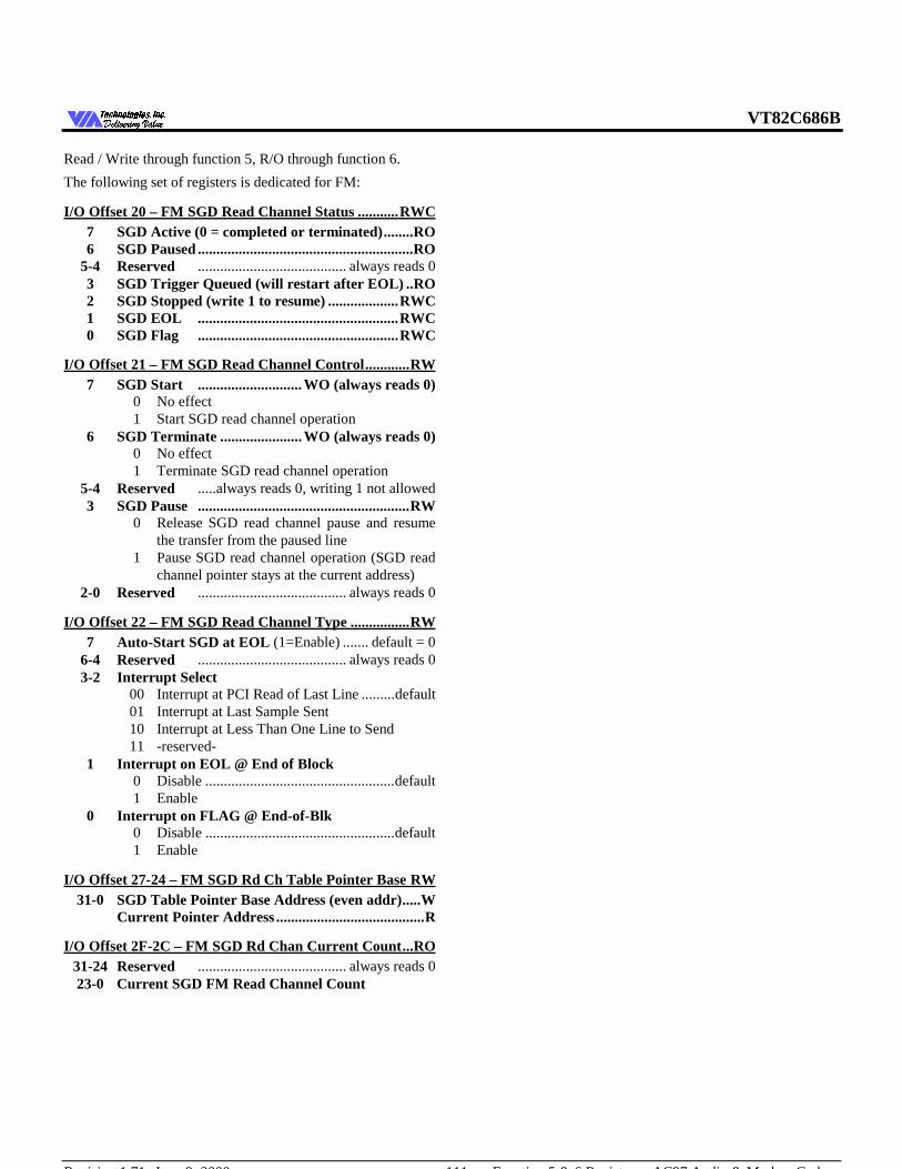
VT82C686B
Revision 1.71 June 9, 2000 -111- Function 5 & 6 Registers - AC97 Audio & Modem Codecs
7HFKQRORJLHV ,QF'HOLYHULQJ 9DOXH'HOLYHULQJ 9DOXH
Read / Write through function 5, R/O through function 6.
The following set of registers is dedicated for FM:
I/O Offset 20 – FM SGD Read Channel Status ........... RWC7 SGD Active (0 = completed or terminated)........RO6 SGD Paused ..........................................................RO
5-4 Reserved ........................................ always reads 03 SGD Trigger Queued (will restart after EOL) ..RO2 SGD Stopped (write 1 to resume) ...................RWC1 SGD EOL ......................................................RWC0 SGD Flag ......................................................RWC
I/O Offset 21 – FM SGD Read Channel Control ............ RW7 SGD Start ............................ WO (always reads 0)
0 No effect1 Start SGD read channel operation
6 SGD Terminate ...................... WO (always reads 0)0 No effect1 Terminate SGD read channel operation
5-4 Reserved .....always reads 0, writing 1 not allowed3 SGD Pause .........................................................RW
0 Release SGD read channel pause and resumethe transfer from the paused line
1 Pause SGD read channel operation (SGD readchannel pointer stays at the current address)
2-0 Reserved ........................................ always reads 0
I/O Offset 22 – FM SGD Read Channel Type ................ RW7 Auto-Start SGD at EOL (1=Enable) ....... default = 0
6-4 Reserved ........................................ always reads 03-2 Interrupt Select
00 Interrupt at PCI Read of Last Line .........default01 Interrupt at Last Sample Sent10 Interrupt at Less Than One Line to Send11 -reserved-
1 Interrupt on EOL @ End of Block0 Disable ...................................................default1 Enable
0 Interrupt on FLAG @ End-of-Blk0 Disable ...................................................default1 Enable
I/O Offset 27-24 – FM SGD Rd Ch Table Pointer Base RW31-0 SGD Table Pointer Base Address (even addr).....W
Current Pointer Address ........................................R
I/O Offset 2F-2C – FM SGD Rd Chan Current Count ... RO31-24 Reserved ........................................ always reads 023-0 Current SGD FM Read Channel Count
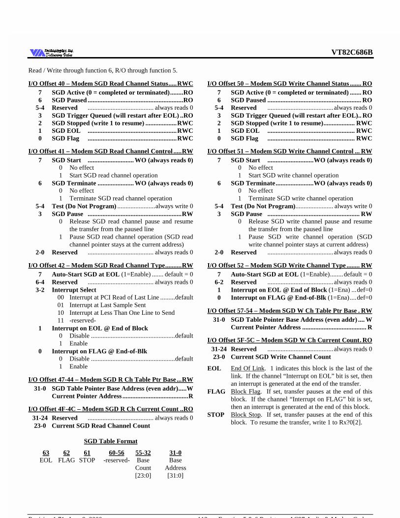
VT82C686B
Revision 1.71 June 9, 2000 -112- Function 5 & 6 Registers - AC97 Audio & Modem Codecs
7HFKQRORJLHV ,QF'HOLYHULQJ 9DOXH'HOLYHULQJ 9DOXH
Read / Write through function 6, R/O through function 5.
I/O Offset 40 – Modem SGD Read Channel Status ..... RWC7 SGD Active (0 = completed or terminated)........RO6 SGD Paused ..........................................................RO
5-4 Reserved ........................................ always reads 03 SGD Trigger Queued (will restart after EOL) ..RO2 SGD Stopped (write 1 to resume) ...................RWC1 SGD EOL ......................................................RWC0 SGD Flag ......................................................RWC
I/O Offset 41 – Modem SGD Read Channel Control ..... RW7 SGD Start ............................ WO (always reads 0)
0 No effect1 Start SGD read channel operation
6 SGD Terminate ...................... WO (always reads 0)0 No effect1 Terminate SGD read channel operation
5-4 Test (Do Not Program) .......................always write 03 SGD Pause .........................................................RW
0 Release SGD read channel pause and resumethe transfer from the paused line
1 Pause SGD read channel operation (SGD readchannel pointer stays at the current address)
2-0 Reserved ........................................ always reads 0
I/O Offset 42 – Modem SGD Read Channel Type .......... RW7 Auto-Start SGD at EOL (1=Enable) ....... default = 0
6-4 Reserved ........................................ always reads 03-2 Interrupt Select
00 Interrupt at PCI Read of Last Line .........default01 Interrupt at Last Sample Sent10 Interrupt at Less Than One Line to Send11 -reserved-
1 Interrupt on EOL @ End of Block0 Disable ...................................................default1 Enable
0 Interrupt on FLAG @ End-of-Blk0 Disable ...................................................default1 Enable
I/O Offset 47-44 – Modem SGD R Ch Table Ptr Base ... RW31-0 SGD Table Pointer Base Address (even addr).....W
Current Pointer Address ........................................R
I/O Offset 4F-4C – Modem SGD R Ch Current Count .. RO31-24 Reserved ........................................ always reads 023-0 Current SGD Read Channel Count
SGD Table Format
63 62 61 60-56 55-32 31-0EOL FLAG STOP -reserved- Base Base
Count Address[23:0] [31:0]
I/O Offset 50 – Modem SGD Write Channel Status ....... RO7 SGD Active (0 = completed or terminated) ....... RO6 SGD Paused ......................................................... RO
5-4 Reserved ........................................always reads 03 SGD Trigger Queued (will restart after EOL).. RO2 SGD Stopped (write 1 to resume)................... RWC1 SGD EOL ..................................................... RWC0 SGD Flag ..................................................... RWC
I/O Offset 51 – Modem SGD Write Channel Control ... RW7 SGD Start ............................WO (always reads 0)
0 No effect1 Start SGD write channel operation
6 SGD Terminate.......................WO (always reads 0)0 No effect1 Terminate SGD write channel operation
5-4 Test (Do Not Program)....................... always write 03 SGD Pause ........................................................ RW
0 Release SGD write channel pause and resumethe transfer from the paused line
1 Pause SGD write channel operation (SGDwrite channel pointer stays at current address)
2-0 Reserved ........................................always reads 0
I/O Offset 52 – Modem SGD Write Channel Type ........ RW7 Auto-Start SGD at EOL (1=Enable)........default = 0
6-2 Reserved ........................................always reads 01 Interrupt on EOL @ End of Block (1=Ena) ...def=00 Interrupt on FLAG @ End-of-Blk (1=Ena)....def=0
I/O Offset 57-54 – Modem SGD W Ch Table Ptr Base . RW31-0 SGD Table Pointer Base Address (even addr) .... W
Current Pointer Address ....................................... R
I/O Offset 5F-5C – Modem SGD W Ch Current Count . RO31-24 Reserved ........................................always reads 023-0 Current SGD Write Channel Count
EOL End Of Link. 1 indicates this block is the last of thelink. If the channel “Interrupt on EOL” bit is set, thenan interrupt is generated at the end of the transfer.
FLAG Block Flag. If set, transfer pauses at the end of thisblock. If the channel “Interrupt on FLAG” bit is set,then an interrupt is generated at the end of this block.
STOP Block Stop. If set, transfer pauses at the end of thisblock. To resume the transfer, write 1 to Rx?0[2].
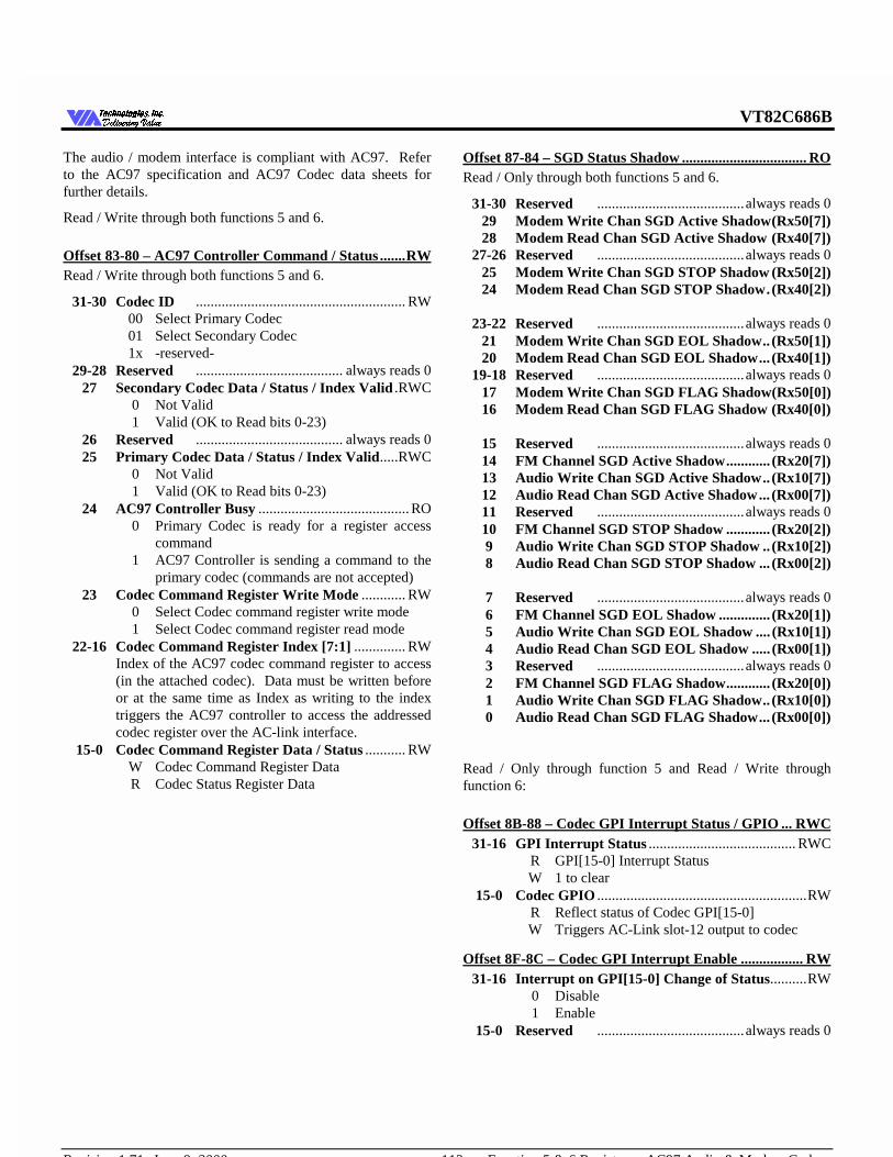
VT82C686B
Revision 1.71 June 9, 2000 -113- Function 5 & 6 Registers - AC97 Audio & Modem Codecs
7HFKQRORJLHV ,QF'HOLYHULQJ 9DOXH'HOLYHULQJ 9DOXH
The audio / modem interface is compliant with AC97. Referto the AC97 specification and AC97 Codec data sheets forfurther details.
Read / Write through both functions 5 and 6.
Offset 83-80 – AC97 Controller Command / Status ....... RWRead / Write through both functions 5 and 6.
31-30 Codec ID ......................................................... RW00 Select Primary Codec01 Select Secondary Codec1x -reserved-
29-28 Reserved ........................................ always reads 027 Secondary Codec Data / Status / Index Valid .RWC
0 Not Valid1 Valid (OK to Read bits 0-23)
26 Reserved ........................................ always reads 025 Primary Codec Data / Status / Index Valid.....RWC
0 Not Valid1 Valid (OK to Read bits 0-23)
24 AC97 Controller Busy ......................................... RO0 Primary Codec is ready for a register access
command1 AC97 Controller is sending a command to the
primary codec (commands are not accepted)23 Codec Command Register Write Mode ............ RW
0 Select Codec command register write mode1 Select Codec command register read mode
22-16 Codec Command Register Index [7:1] .............. RWIndex of the AC97 codec command register to access(in the attached codec). Data must be written beforeor at the same time as Index as writing to the indextriggers the AC97 controller to access the addressedcodec register over the AC-link interface.
15-0 Codec Command Register Data / Status ........... RWW Codec Command Register DataR Codec Status Register Data
Offset 87-84 – SGD Status Shadow .................................. RORead / Only through both functions 5 and 6.
31-30 Reserved ........................................always reads 029 Modem Write Chan SGD Active Shadow(Rx50[7])28 Modem Read Chan SGD Active Shadow (Rx40[7])
27-26 Reserved ........................................always reads 025 Modem Write Chan SGD STOP Shadow (Rx50[2])24 Modem Read Chan SGD STOP Shadow.(Rx40[2])
23-22 Reserved ........................................always reads 021 Modem Write Chan SGD EOL Shadow.. (Rx50[1])20 Modem Read Chan SGD EOL Shadow... (Rx40[1])
19-18 Reserved ........................................always reads 017 Modem Write Chan SGD FLAG Shadow(Rx50[0])16 Modem Read Chan SGD FLAG Shadow (Rx40[0])
15 Reserved ........................................always reads 014 FM Channel SGD Active Shadow............ (Rx20[7])13 Audio Write Chan SGD Active Shadow.. (Rx10[7])12 Audio Read Chan SGD Active Shadow... (Rx00[7])11 Reserved ........................................always reads 010 FM Channel SGD STOP Shadow ............ (Rx20[2])9 Audio Write Chan SGD STOP Shadow .. (Rx10[2])8 Audio Read Chan SGD STOP Shadow ... (Rx00[2])
7 Reserved ........................................always reads 06 FM Channel SGD EOL Shadow .............. (Rx20[1])5 Audio Write Chan SGD EOL Shadow .... (Rx10[1])4 Audio Read Chan SGD EOL Shadow ..... (Rx00[1])3 Reserved ........................................always reads 02 FM Channel SGD FLAG Shadow............ (Rx20[0])1 Audio Write Chan SGD FLAG Shadow.. (Rx10[0])0 Audio Read Chan SGD FLAG Shadow... (Rx00[0])
Read / Only through function 5 and Read / Write throughfunction 6:
Offset 8B-88 – Codec GPI Interrupt Status / GPIO ... RWC31-16 GPI Interrupt Status ........................................ RWC
R GPI[15-0] Interrupt StatusW 1 to clear
15-0 Codec GPIO .........................................................RWR Reflect status of Codec GPI[15-0]W Triggers AC-Link slot-12 output to codec
Offset 8F-8C – Codec GPI Interrupt Enable ................. RW31-16 Interrupt on GPI[15-0] Change of Status..........RW
0 Disable1 Enable
15-0 Reserved ........................................always reads 0
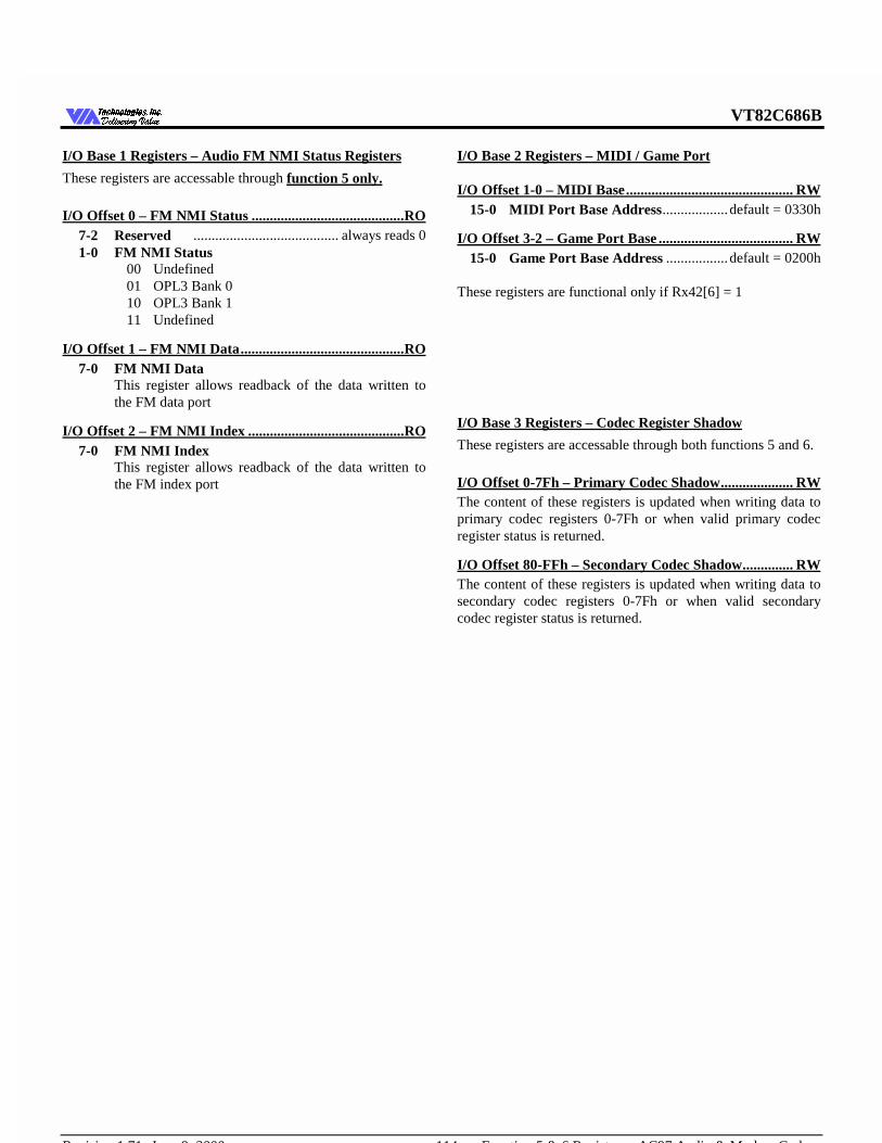
VT82C686B
Revision 1.71 June 9, 2000 -114- Function 5 & 6 Registers - AC97 Audio & Modem Codecs
7HFKQRORJLHV ,QF'HOLYHULQJ 9DOXH'HOLYHULQJ 9DOXH
I/O Base 1 Registers – Audio FM NMI Status Registers
These registers are accessable through function 5 only.
I/O Offset 0 – FM NMI Status .......................................... RO7-2 Reserved ........................................ always reads 01-0 FM NMI Status
00 Undefined01 OPL3 Bank 010 OPL3 Bank 111 Undefined
I/O Offset 1 – FM NMI Data ............................................. RO7-0 FM NMI Data
This register allows readback of the data written tothe FM data port
I/O Offset 2 – FM NMI Index ........................................... RO7-0 FM NMI Index
This register allows readback of the data written tothe FM index port
I/O Base 2 Registers – MIDI / Game Port
I/O Offset 1-0 – MIDI Base .............................................. RW15-0 MIDI Port Base Address..................default = 0330h
I/O Offset 3-2 – Game Port Base ..................................... RW15-0 Game Port Base Address .................default = 0200h
These registers are functional only if Rx42[6] = 1
I/O Base 3 Registers – Codec Register Shadow
These registers are accessable through both functions 5 and 6.
I/O Offset 0-7Fh – Primary Codec Shadow .................... RWThe content of these registers is updated when writing data toprimary codec registers 0-7Fh or when valid primary codecregister status is returned.
I/O Offset 80-FFh – Secondary Codec Shadow .............. RWThe content of these registers is updated when writing data tosecondary codec registers 0-7Fh or when valid secondarycodec register status is returned.
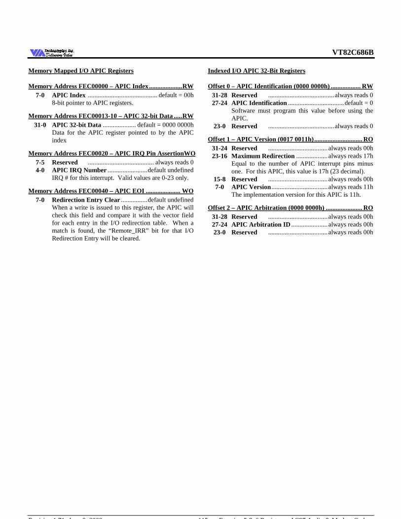
VT82C686B
Revision 1.71 June 9, 2000 -115- Function 5 & 6 Registers - AC97 Audio & Modem Codecs
7HFKQRORJLHV ,QF'HOLYHULQJ 9DOXH'HOLYHULQJ 9DOXH
Memory Mapped I/O APIC Registers
Memory Address FEC00000 – APIC Index .................... RW7-0 APIC Index .......................................... default = 00h
8-bit pointer to APIC registers.
Memory Address FEC00013-10 – APIC 32-bit Data ..... RW31-0 APIC 32-bit Data .................... default = 0000 0000h
Data for the APIC register pointed to by the APICindex
Memory Address FEC00020 – APIC IRQ Pin Assertion WO7-5 Reserved ........................................ always reads 04-0 APIC IRQ Number ........................default undefined
IRQ # for this interrupt. Valid values are 0-23 only.
Memory Address FEC00040 – APIC EOI ..................... WO7-0 Redirection Entry Clear ................default undefined
When a write is issued to this register, the APIC willcheck this field and compare it with the vector fieldfor each entry in the I/O redirection table. When amatch is found, the “Remote_IRR” bit for that I/ORedirection Entry will be cleared.
Indexed I/O APIC 32-Bit Registers
Offset 0 – APIC Identification (0000 0000h) .................. RW31-28 Reserved ........................................always reads 027-24 APIC Identification ..................................default = 0
Software must program this value before using theAPIC.
23-0 Reserved ........................................always reads 0
Offset 1 – APIC Version (0017 0011h) ............................. RO31-24 Reserved .................................... always reads 00h23-16 Maximum Redirection ................... always reads 17h
Equal to the number of APIC interrupt pins minusone. For this APIC, this value is 17h (23 decimal).
15-8 Reserved .................................... always reads 00h7-0 APIC Version.................................. always reads 11h
The implementation version for this APIC is 11h.
Offset 2 – APIC Arbitration (0000 0000h) ...................... RO31-28 Reserved .................................... always reads 00h27-24 APIC Arbitration ID ...................... always reads 00h23-0 Reserved .................................... always reads 00h
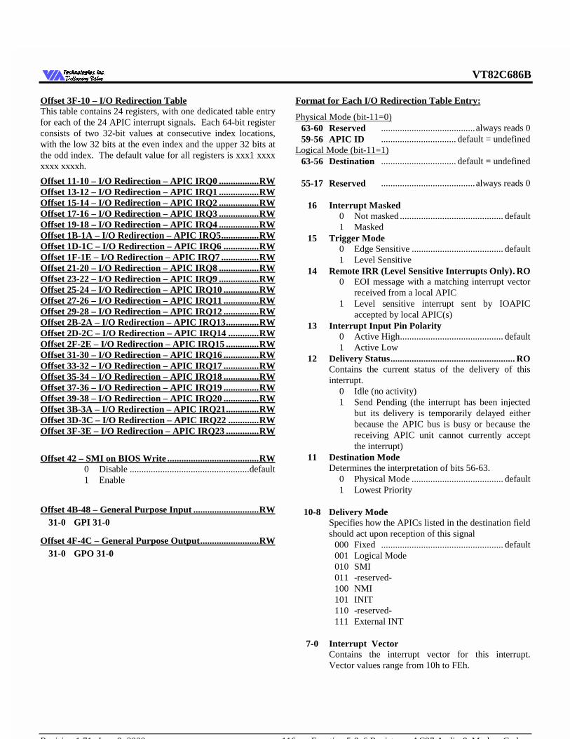
VT82C686B
Revision 1.71 June 9, 2000 -116- Function 5 & 6 Registers - AC97 Audio & Modem Codecs
7HFKQRORJLHV ,QF'HOLYHULQJ 9DOXH'HOLYHULQJ 9DOXH
Offset 3F-10 – I/O Redirection TableThis table contains 24 registers, with one dedicated table entryfor each of the 24 APIC interrupt signals. Each 64-bit registerconsists of two 32-bit values at consecutive index locations,with the low 32 bits at the even index and the upper 32 bits atthe odd index. The default value for all registers is xxx1 xxxxxxxx xxxxh.
Offset 11-10 – I/O Redirection – APIC IRQ0 ................. RWOffset 13-12 – I/O Redirection – APIC IRQ1 ................. RWOffset 15-14 – I/O Redirection – APIC IRQ2 ................. RWOffset 17-16 – I/O Redirection – APIC IRQ3 ................. RWOffset 19-18 – I/O Redirection – APIC IRQ4 ................. RWOffset 1B-1A – I/O Redirection – APIC IRQ5 ................ RWOffset 1D-1C – I/O Redirection – APIC IRQ6 ............... RWOffset 1F-1E – I/O Redirection – APIC IRQ7 ................ RWOffset 21-20 – I/O Redirection – APIC IRQ8 ................. RWOffset 23-22 – I/O Redirection – APIC IRQ9 ................. RWOffset 25-24 – I/O Redirection – APIC IRQ10 ............... RWOffset 27-26 – I/O Redirection – APIC IRQ11 ............... RWOffset 29-28 – I/O Redirection – APIC IRQ12 ............... RWOffset 2B-2A – I/O Redirection – APIC IRQ13 .............. RWOffset 2D-2C – I/O Redirection – APIC IRQ14 ............. RWOffset 2F-2E – I/O Redirection – APIC IRQ15 .............. RWOffset 31-30 – I/O Redirection – APIC IRQ16 ............... RWOffset 33-32 – I/O Redirection – APIC IRQ17 ............... RWOffset 35-34 – I/O Redirection – APIC IRQ18 ............... RWOffset 37-36 – I/O Redirection – APIC IRQ19 ............... RWOffset 39-38 – I/O Redirection – APIC IRQ20 ............... RWOffset 3B-3A – I/O Redirection – APIC IRQ21 .............. RWOffset 3D-3C – I/O Redirection – APIC IRQ22 ............. RWOffset 3F-3E – I/O Redirection – APIC IRQ23 .............. RW
Offset 42 – SMI on BIOS Write ....................................... RW0 Disable ...................................................default1 Enable
Offset 4B-48 – General Purpose Input ............................ RW31-0 GPI 31-0
Offset 4F-4C – General Purpose Output ......................... RW31-0 GPO 31-0
Format for Each I/O Redirection Table Entry:
Physical Mode (bit-11=0)63-60 Reserved ........................................always reads 059-56 APIC ID ................................ default = undefined
Logical Mode (bit-11=1)63-56 Destination ................................ default = undefined
55-17 Reserved ........................................always reads 0
16 Interrupt Masked0 Not masked ............................................ default1 Masked
15 Trigger Mode0 Edge Sensitive ....................................... default1 Level Sensitive
14 Remote IRR (Level Sensitive Interrupts Only). RO0 EOI message with a matching interrupt vector
received from a local APIC1 Level sensitive interrupt sent by IOAPIC
accepted by local APIC(s)13 Interrupt Input Pin Polarity
0 Active High............................................ default1 Active Low
12 Delivery Status..................................................... ROContains the current status of the delivery of thisinterrupt.
0 Idle (no activity)1 Send Pending (the interrupt has been injected
but its delivery is temporarily delayed eitherbecause the APIC bus is busy or because thereceiving APIC unit cannot currently acceptthe interrupt)
11 Destination ModeDetermines the interpretation of bits 56-63.
0 Physical Mode ....................................... default1 Lowest Priority
10-8 Delivery ModeSpecifies how the APICs listed in the destination fieldshould act upon reception of this signal
000 Fixed .................................................... default001 Logical Mode010 SMI011 -reserved-100 NMI101 INIT110 -reserved-111 External INT
7-0 Interrupt VectorContains the interrupt vector for this interrupt.Vector values range from 10h to FEh.
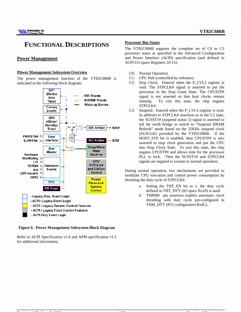
VT82C686B
Revision 1.71 June 9, 2000 -117- Functional Descriptions
7HFKQRORJLHV ,QF'HOLYHULQJ 9DOXH'HOLYHULQJ 9DOXH
FUNCTIONAL DESCRIPTIONS
Power Management
Power Management Subsystem Overview
The power management function of the VT82C686B isindicated in the following block diagram:
7+50
3RZHU
3ODQH DQG
6\VWHP
&RQWURO
*3
*OREDO
6WDQGE\
7LPHU
3:5%71
5,
60, $UELWHU
6OHHS:DNH
6WDWH
0DFKLQH
60,
6&,
/HJDF\ 2QO\ (YHQW /RJLF
$&3, /HJDF\ (YHQW /RJLF
$&3, 2QO\ (YHQW /RJLF
60, (YHQWV
6&,60, (YHQWV
'HF
&38
673&/.
DQG &ON*HQ
&RQWURO
*3
'HYLFH
,GOH
7LPHU
8VHU
,QWHUIDFH
+DUGZDUH
(YHQWV
57&
6&,B(1
$&3, /HJDF\ *HQHULF &RQWURO )HDWXUHV
$&3, /HJDF\ )L[HG &RQWURO )HDWXUHV
:DNHXS (YHQWV
30 7LPHU
6&, $UELWHU
%XV
0DVWHU
6/3%71
3ULPDU\
(YHQWV
86% UHVXPH
/,'
*3,2
+DUGZDUH
0RQLWRULQJ
Figure 6. Power Management Subsystem Block Diagram
Refer to ACPI Specification v1.0 and APM specification v1.2for additional information.
Processor Bus States
The VT82C686B supports the complete set of C0 to C3processor states as specified in the Advanced Configurationand Power Interface (ACPI) specification (and defined inACPI I/O space Registers 10-15):
C0: Normal OperationC1: CPU Halt (controlled by software).C2: Stop Clock. Entered when the P_LVL2 register is
read. The STPCLK# signal is asserted to put theprocessor in the Stop Grant State. The CPUSTP#signal is not asserted so that host clocks remainrunning. To exit this state, the chip negatesSTPCLK#.
C3: Suspend. Entered when the P_LVL3 register is read.In addition to STPCLK# assertion as in the C2 state,the SUSST1# (suspend status 1) signal is asserted totell the north bridge to switch to “Suspend DRAMRefresh” mode based on the 32KHz suspend clock(SUSCLK) provided by the VT82C686B. If theHOST_STP bit is enabled, then CPUSTP# is alsoasserted to stop clock generation and put the CPUinto Stop Clock State. To exit this state, the chipnegates CPUSTP# and allows time for the processorPLL to lock. Then the SUSST1# and STPCLK#signals are negated to resume to normal operation.
During normal operation, two mechanisms are provided tomodulate CPU execution and control power consumption bythrottling the duty cycle of STPCLK#:
a. Setting the THT_EN bit to 1, the duty cycledefined in THT_DTY (IO space Rx10) is used.
b. THRM# pin assertion enables automatic clockthrottling with duty cycle pre-configured inTHM_DTY (PCI configuration Rx4C).
VT82C686B
Revision 1.71 June 9, 2000 -118- Functional Descriptions
7HFKQRORJLHV ,QF'HOLYHULQJ 9DOXH'HOLYHULQJ 9DOXH
System Suspend States and Power Plane Control
There are three power planes inside the VT82C686B. Thefirst power plane (VCCS) is always on unless turned off by themechanical switch. The second power plane (VCC) iscontrolled by chip output SUSC# (also called “PSON”). Thethird plane (VCCRTC) is powered by the combination of theVCCS and the external battery (VBAT) for the integrated realtime clock. Most of the circuitry inside the VT82C686B ispowered by VCC. The amount of logic powered by VCCS isvery small; its main function is to control the supply of VCCand other power planes. VCCRTC is always on unless both themechanical switch and VBAT are removed.
The VT82C686B supports multiple system suspend states byconfiguring the SLP_TYP field of ACPI I/O space registerRx4-5:
a) POS (Power On Suspend): Most devices in thesystem remain powered. The host bus is put into anequivalent of the C3 state. In particular, the CPU isput into the Stop Grant State or Stop Clock Statedepending on the setting of the HOST_STP bit.SUSST1# is asserted to tell the north bridge to switchto “Suspend DRAM Refresh” mode based on the32KHz SUSCLK provided by the VT82C686B. Asto the PCI bus, setting the PCLK_RUN bit to 0enables the CLKRUN protocol defined in the PCIMobile Design Guide. That is, the PCKRUN# pinwill be de-activated after the PCI bus is idle for 26clocks. Any PCI bus masters including the northbridge may resume PCI clock operation by pullingthe PCKRUN# pin low. During the PCKRUN# de-activation period, the PCISTP# pin may be activatedto disable the output of the PCI clock generator if thePCI_STP bit is enabled. When the system resumesfrom POS, the VT82C686B can optionally resumewithout resetting the system, can reset the processoronly, or can reset the entire system. When no reset isperformed, the chip only needs to wait for the clocksynthesizer and processor PLL to lock before thesystem is resumed, which typically takes 20ms.
b) STR (Suspend to RAM): Power is removed frommost of the system except the system DRAM. Poweris supplied to the suspend refresh logic in the northbridge (VTT of VT82C598) and the suspend logic ofthe VT82C686B (VCCS). The VT82C686Bprovides a 32KHz suspend clock to the north bridgefor it to use to continue DRAM refresh.
c) STD (Suspend to Disk, also called Soft-off): Poweris removed from most of the system except thesuspend logic of VT82C686B (VCCS).
d) Mechanical Off: This is not a suspend state. Allpower in the system is removed except the RTCbattery.
The suspend state is entered by setting the SLP_EN bit to 1.Three power plane control signals (SUSA#, SUSB# and
SUSC#) are provided to turn off more system power planes asthe system moves to deeper power-down states, i.e., fromnormal operation to POS (only SUSA# asserted), to STR (bothSUSA# and SUSB# asserted), and to STD (all three SUS#signals asserted). In particular, the assertion of SUSC# can beused to turn off the VCC supply to the VT82C686B.
One additional suspend status indicator (SUSST1#) isprovided to inform the north bridge and the rest of the systemof the processor and system suspend states. SUSST1# isasserted when the system enters the suspend state or theprocessor enters the C3 state. SUSST1# is connected to thenorth bridge to switch between normal and suspend-DRAM-refresh modes.
General Purpose I/O Ports
As ACPI compliant hardware, the VT82C686B includesPWRBTN#, SLPBTN#, and RI# pins to implement powerbutton, sleep button, and ring indicator functionality,respectively. Furthermore, the VT82C686B offers manygeneral-purpose I/O ports with the following capabilities:
• I2C/SMB Support• Thermal Detect• Notebook Lid Open/Close Detect• Battery Low Detect• Twelve General Purpose Input Ports (multiplexed with
other functions).
• Nineteen General Purpose Output Ports (1 dedicatedand 18 multiplexed with other functions)
• Four General Purpose Input / Output Ports(multiplexed with other functions)
In addition, the VT82C686B provides an external dedicatedSMI pin (EXTSMI#). The external SMI input can beprogrammed to trigger an SCI or SMI at both the rising andfalling edges of the corresponding input signal. Software cancheck the status of the input pin and take appropriate actions.
VT82C686B
Revision 1.71 June 9, 2000 -119- Functional Descriptions
7HFKQRORJLHV ,QF'HOLYHULQJ 9DOXH'HOLYHULQJ 9DOXH
Power Management Events
Three types of power management events are supported:
1) ACPI-required Fixed Events defined in the PM1a_STSand PM1a_EN registers. These events can trigger eitherSCI or SMI depending on the SCI_EN bit:
• PWRBTN# Triggering• RTC Alarm• Sleep Button• ACPI Power Management Timer Carry (always SCI)• BIOS Release (always SCI)
2) ACPI-aware General Purpose Function Events definedin the GP_STS and GP_SCI_EN, and GP_SMI_ENregisters. These events can trigger either SCI or SMIdepending on the setting of individual SMI and SCIenable bits:
• External SMI triggering• USB Resume• Ring Indicator (RI#)• Battery Low Detect (BATLOW#)• Notebook Lid Open/Close Detect (LID)• Thermal Detect (THRM#)
3) Generic Global Events defined in the GBL_STS andGBL_EN registers. These registers are mainly used forSMI:
• PCI Bus Clock Run Resume• Primary Interrupt Occurance• GP0 and GP1 Timer Time Out• Secondary Event Timer Time Out• Occurrence of Primary Events
(defined in register PACT_STS and PACT_EN)• Legacy USB accesses (keyboard and mouse)- Software SMI
System and Processor Resume Events
Depending on the system suspend state, different features canbe enabled to resume the system. There are two classes ofresume events:
a) VCCS-based events. Event logic resides in theVCCS plane and thus can resume the system fromany suspend state. Such events include PWRBTN#,RI#, BATLOW#, LID, SMBus resume event, RTCalarm, EXTSMI#, and GP1 (EXTSMI1#).
b) VCC-Based Events. Event logic resides in the VCCplane and thus can only resume the system from thePOS state. Such events include the ACPI PM timer,USB resume, and EXTSMIn#.
PCKRUN# PCLK
HCLKGCLK
Host CPU
CPU Bus
CKE#
Memory Bus
SMBusISA
VT82C598(Apollo MVP3)
orVT82C693
(Apollo ProPlus)
FPG, EDO, orSDRAM
(SDR or DDR)
3DGraphics
Controller
AGP Bus
PCISTP#
GPIO and ACPI EventsBIOS ROM
L2 Cache(Socket-7 Only)
GCKRUN#
PCI Bus
IDE
USBPower Plane & Peripheral Control
VT82C686ASuper South
Keyboard / Mouse
CPUSTP# ClockGenerator
MCLK
HCLK
GCLK
PCLK
SMI# / STPCLK#
SUSCLK,SUSST1#
SMIACT#
Module ID
Figure 7. System Block Diagram Using the VT82C686B Super South Bridge
VT82C686B
Revision 1.71 June 9, 2000 -120- Functional Descriptions
7HFKQRORJLHV ,QF'HOLYHULQJ 9DOXH'HOLYHULQJ 9DOXH
Legacy Power Management Timers
In addition to the ACPI power management timer, theVT82C686B includes the following four legacy powermanagement timers:
GP0 Timer: general purpose timer with primary event
GP1 Timer: general purpose timer with peripheral eventreload
Secondary Event Timer: to monitor secondary events
Conserve Mode Timer: Hardware-controlled return tostandby
The normal sequence of operations for a general purpose timer(GP0 or GP1) is to
1) First program the time base and timer value of the initialcount (register GP_TIM_CNT).
2) Then activate counting by setting the GP0_START orGP1_START bit to one: the timer will start with theinitial count and count down towards 0.
3) When the timer counts down to zero, an SMI will begenerated if enabled (GP0TO_EN and GP1TO_EN in theGBL_EN register) with status recorded (GP0TO_STS andGP1TO_STS in the GBL_STS register).
4) Each timer can also be programmed to reload the initialcount and restart counting automatically after countingdown to 0. This feature is not used in standard VIABIOS.
The GP0 and GP1 timers can be used just as the generalpurpose timers described above. However, they can also beprogrammed to reload the initial count by system primaryevents or peripheral events thus used as primary event (globalstandby) timer and peripheral timer, respectively. Thesecondary event timer is solely used to monitor secondaryevents.
System Primary and Secondary Events
Primary system events are distinguished in the PRI_ACT_STSand PRI_ACT_EN registers:
Bit Event Trigger7 Keyboard Access I/O port 60h6 Serial Port Access I/O ports 3F8h-3FFh, 2F8h-2FFh,
3E8h-3EFh, or 2E8h-2EFh5 Parallel Port Access I/O ports 378h-37Fh or 278h-27Fh4 Video Access I/O ports 3B0h-3DFh or memory
A/B segments3 IDE/Floppy Access I/O ports 1F0h-1F7h, 170h-177h,
or 3F5h2 Reserved1 Primary Interrupts Each channel of the interrupt
controller can be programmed tobe a primary or secondaryinterrupt
0 ISA Master/DMA ActivityEach category can be enabled as a primary event by setting thecorresponding bit of the PRI_ACT_EN register to 1. If
enabled, the occurrence of the primary event reloads the GP0timer if the PACT_GP0_EN bit is also set to 1. The cause ofthe timer reload is recorded in the corresponding bit ofPRI_ACT_STS register while the timer is reloaded. If noenabled primary event occurs during the count down, the GP0timer will time out (count down to 0) and the system can beprogrammed (setting the GP0TO_EN bit in the GBL_ENregister to one) to trigger an SMI to switch the system to apower down mode.
The VT82C686B distinguishes two kinds of interrupt requestsas far as power management is concerned: the primary andsecondary interrupts. Like other primary events, theoccurrence of a primary interrupt demands that the system berestored to full processing capability. Secondary interrupts,however, are typically used for housekeeping tasks in thebackground unnoticeable to the user. The VT82C686B allowseach channel of interrupt request to be declared as eitherprimary, secondary, or ignorable in the PIRQ_CH andSIRQ_CH registers. Secondary interrupts are the only systemsecondary events defined in the VT82C686B.
Like primary events, primary interrupts can be made to reloadthe GP0 timer by setting the PIRQ_EN bit to 1. Secondaryinterrupts do not reload the GP0 timer. Therefore the GP0timer will time out and the SMI routine can put the system intopower down mode if no events other than secondary interruptsare happening periodically in the background.
Primary events can be programmed to trigger an SMI (settingof the PACT_EN bit). Typically, this SMI triggering is turnedoff during normal system operation to avoid degrading systemperformance. Triggering is turned on by the SMI routinebefore entering the power down mode so that the system maybe returned to normal operation at the occurrence of primaryevents. At the same time, the GP0 timer is reloaded and thecount down process is restarted.
Peripheral Events
Primary and secondary events define system events in generaland the response is typically expressed in terms of systemevents. Individual peripheral events can also be monitored bythe VT82C686B through the GP1 timer. The following fourcategories of peripheral events are distinguished (via registerGP_RLD_EN):
Bit-7 Keyboard AccessBit-6 Serial Port AccessBit-4 Video AccessBit-3 IDE/Floppy Access
The four categories are subsets of the primary events asdefined in PRI_ACT_EN and the occurrence of these eventscan be checked through a common register PRI_ACT_STS.As a peripheral timer, GP1 can be used to monitor one (ormore than one) of the above four device types by programmingthe corresponding bit to one and the other bits to zero. Timeout of the GP1 timer indicates no activity of the correspondingdevice type and appropriate action can be taken as a result.
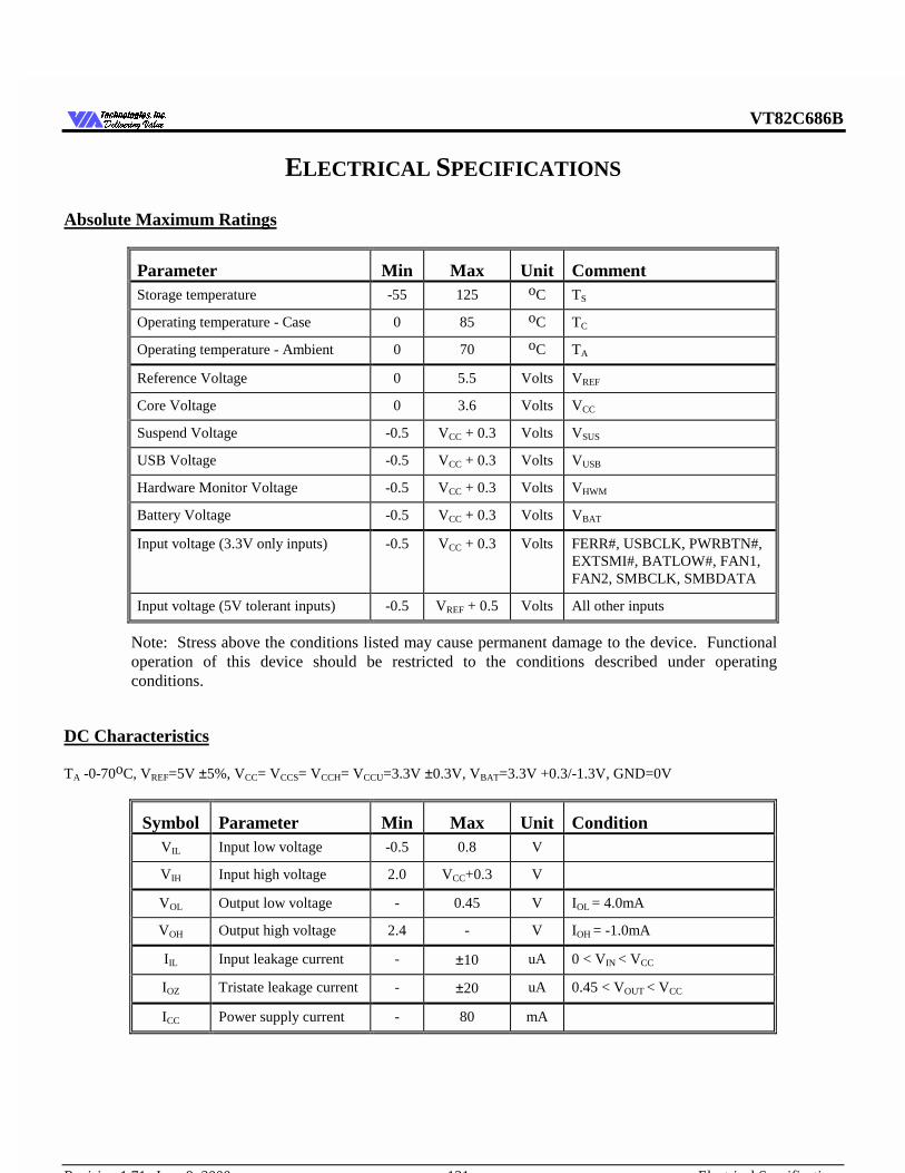
VT82C686B
Revision 1.71 June 9, 2000 -121- Electrical Specifications
7HFKQRORJLHV ,QF'HOLYHULQJ 9DOXH'HOLYHULQJ 9DOXH
ELECTRICAL SPECIFICATIONS
Absolute Maximum Ratings
Parameter Min Max Unit CommentStorage temperature -55 125 oC TS
Operating temperature - Case 0 85 oC TC
Operating temperature - Ambient 0 70 oC TA
Reference Voltage 0 5.5 Volts VREF
Core Voltage 0 3.6 Volts VCC
Suspend Voltage -0.5 VCC + 0.3 Volts VSUS
USB Voltage -0.5 VCC + 0.3 Volts VUSB
Hardware Monitor Voltage -0.5 VCC + 0.3 Volts VHWM
Battery Voltage -0.5 VCC + 0.3 Volts VBAT
Input voltage (3.3V only inputs) -0.5 VCC + 0.3 Volts FERR#, USBCLK, PWRBTN#,EXTSMI#, BATLOW#, FAN1,FAN2, SMBCLK, SMBDATA
Input voltage (5V tolerant inputs) -0.5 VREF + 0.5 Volts All other inputs
Note: Stress above the conditions listed may cause permanent damage to the device. Functionaloperation of this device should be restricted to the conditions described under operatingconditions.
DC Characteristics
TA -0-70oC, VREF=5V ±5%, VCC= VCCS= VCCH= VCCU=3.3V ±0.3V, VBAT=3.3V +0.3/-1.3V, GND=0V
Symbol Parameter Min Max Unit ConditionVIL Input low voltage -0.5 0.8 V
VIH Input high voltage 2.0 VCC+0.3 V
VOL Output low voltage - 0.45 V IOL = 4.0mA
VOH Output high voltage 2.4 - V IOH = -1.0mA
IIL Input leakage current - ±10 uA 0 < VIN < VCC
IOZ Tristate leakage current - ±20 uA 0.45 < VOUT < VCC
ICC Power supply current - 80 mA
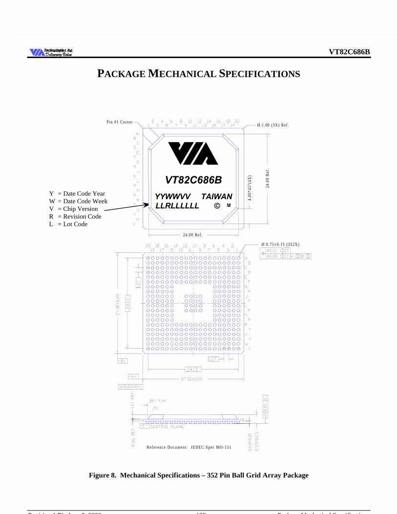
VT82C686B
Revision 1.71 June 9, 2000 -122- Package Mechanical Specifications
7HFKQRORJLHV ,QF'HOLYHULQJ 9DOXH'HOLYHULQJ 9DOXH
PACKAGE MECHANICAL SPECIFICATIONS
Figure 8. Mechanical Specifications – 352 Pin Ball Grid Array Package
>0
Y = Date Code YearW = Date Code WeekV = Chip VersionR = Revision CodeL = Lot Code
4.00
*45°
(4X
)
24.0
0 R
ef.
2 4 .00 Ref .
R e f e r e n c e D o c u m e n t : J E D E C S p e c M O - 1 5 1
Pin #1 Corne rØ 1 .00 (3X) Ref .
Ø 0 . 75±0 .15 (352X)


![Ford ranger new manuel - Blog KiddiQuad · &rs\uljkw .lggl ,qirupdwlrq lpsruwdqwh /h prqwdjh grlw rwuh hiihfwxp xqltxhphqw sdu xq dgxowh dsuqv o¶dvvhpeodjh yhxlooh] ypulilhu vl oh](https://static.fdocuments.fr/doc/165x107/5b7fcc257f8b9ad4778c964e/ford-ranger-new-manuel-blog-rsuljkw-lggl-qirupdwlrq-lpsruwdqwh-h-prqwdjh.jpg)


![Manuel SLS FR...&RS\ULJKW .LGGL 4XDG ± 0(5&('(6 6/6 $0* 9HUVLRQ 9RLWXUH pOHFWULTXH SRXU HQIDQW 0DQXHO GH PRQWDJH 0HUFHGHV %HQ] 6/6 $0* 9HXLOOH] OLUH OH PDQXHO G DVVHPEODJH DYDQW G](https://static.fdocuments.fr/doc/165x107/6016f657951f476d5747b2a3/manuel-sls-fr-rsuljkw-lggl-4xdg-056-66-0-9huvlrq-9rlwxuh.jpg)