
Nikolaou Symeon 200512 Mast
79
DESIGN OF RECONFIGURABLE ANNULAR SLOT ANTENNA (ASA) FOR WIRELESS COMMUNICATIONS / WLAN APPLICATIONS A Thesis Presented to The Academic Faculty by Symeon Nikolaou In Partial Fulfillment of the Requirements for the Degree MASTERS OF SCIENCE IN ELECTRICAL AND COMPUTER ENGINEERING Georgia Institute of Technology December, 2005
Transcript of Nikolaou Symeon 200512 Mast

8/9/2019 Nikolaou Symeon 200512 Mast
http://slidepdf.com/reader/full/nikolaou-symeon-200512-mast 1/79
DESIGN OF RECONFIGURABLE ANNULAR SLOT ANTENNA
(ASA) FOR WIRELESS COMMUNICATIONS / WLAN
APPLICATIONS
A ThesisPresented to
The Academic Faculty
by
Symeon Nikolaou
In Partial Fulfillment
of the Requirements for the DegreeMASTERS OF SCIENCE IN ELECTRICAL AND COMPUTER ENGINEERING
Georgia Institute of Technology
December, 2005

8/9/2019 Nikolaou Symeon 200512 Mast
http://slidepdf.com/reader/full/nikolaou-symeon-200512-mast 2/79
DESIGN OF RECONFIGURABLE ANNULAR SLOT ANTENNA
(ASA) FOR WIRELESS COMMUNICATIONS / WLAN
APPLICATIONS
Approved by:
Dr. John Papapolymerou, AdvisorSchool of Electrical and Computer
Engineering
Georgia Institute of Technology
Dr. Joy LaskarSchool of Electrical and Computer
Engineering
Georgia Institute of Technology
Dr. Manos M. Ttentzeris, Advisor
School of Electrical and Computer
Engineering
Georgia Institute of Technology
Dr. John D. Cressler
School of Electrical and Computer
Engineering
Georgia Institute of Technology
Date Approved: November 22, 2005

8/9/2019 Nikolaou Symeon 200512 Mast
http://slidepdf.com/reader/full/nikolaou-symeon-200512-mast 3/79
To ELEN
for her love, patience and support

8/9/2019 Nikolaou Symeon 200512 Mast
http://slidepdf.com/reader/full/nikolaou-symeon-200512-mast 4/79
iv
ACKNOWLEDGEMENTS
The author wishes to acknowledge the support of the Packaging Research Center
and the Georgia Electronic Design Center. In addition, the author would like to thank
Prof. Manos M. Tentzeris, and Prof. John Papapolymerou for the academic supervision,
Dr. George E. Ponchak, Dr. Ronglin Li, Ramanan Bairavasubramanian, Cesar Lugo,
Dane Thompson, and Ileana Carrasquillo for providing assistance in theoretical
justification and insight, fabrication, and measurement setup used in this research. The
motivation of trying always for the best was instilled into the author’s mind by his
parents Niki Nikolaou and Nikolaos Nikolaou. For that the author is eternally grateful.

8/9/2019 Nikolaou Symeon 200512 Mast
http://slidepdf.com/reader/full/nikolaou-symeon-200512-mast 5/79
v
TABLE OF CONTENTS
Page
ACKNOWLEDGEMENTS…………………………………………………………….. iv
LIST OF TABLES……………………………………………………………………... vii
LIST OF FIGURES…………………………………………………………………… viii
LIST OF SYMBOLS AND ABBREVIATIONS……………………………………… xii
SUMMARY……………………………………………………………………………xiii
CHAPTER 1: INTRODUCTION……………………………………………………….. 1
CHAPTER 2: BACKGROUND………………………………………………………… 5
2.1 MICROSTRIP-FED RECTANGULAR AND ANNULAR SLOT
ANTENNAS…………………………………………………………….. 5
2.2 PAST TECHNIQUES AND APPROACHES…………………………. 12
2.3 PIN DIODES……………………………………………………………15
2.4 SUMMARY……………………………………………………………. 19
CHAPTER 3: FREQUENCY RECONFIGURABLE DESIGN……………………….20
3.1 ANTENNA STRUCTURE…………………………………………….. 20
3.2 DESIGN METHODOLOGY………………………………………….. 23
3.3 FREQUENCY RECONFIGURABLE DESIGN VALIDATION……... 29
3.4 SUMMARY……………………………………………………………. 37
CHAPTER 4: RADIATION PATTERN RECONFIGURABLE DEDSIGN…………. 38
4.1 THEORETICAL ANALYSIS…………………………………………. 39
4.2 NULL POSITION RECONFIGURABLE DESIGN…………………... 49
4.3 RADIATION PATTERN MEASUREMENTS………………………... 52
4.4 SUMMARY ……………………………………………………………58

8/9/2019 Nikolaou Symeon 200512 Mast
http://slidepdf.com/reader/full/nikolaou-symeon-200512-mast 6/79
vi
CHAPTER 5: CONCLUSION AND POTENTIAL APPLICATIONS……………….. 59
APPENDIX A: LIST OF PUBLICATIONS…………………………………………. 61
REFERENCES………………………………………………………………………….62

8/9/2019 Nikolaou Symeon 200512 Mast
http://slidepdf.com/reader/full/nikolaou-symeon-200512-mast 7/79
vii
LIST OF TABLES
Page
Table 1: Antenna structure dimensions………………………………………………… 21
Table 2: Dimensions of circuit elements for frequency reconfigurationand null at 45º……………………………………………………………….. 32
Table 3: Dimensions of circuit elements for null reconfiguration at 5.8 GHz………….50

8/9/2019 Nikolaou Symeon 200512 Mast
http://slidepdf.com/reader/full/nikolaou-symeon-200512-mast 8/79
viii
LIST OF FIGURES
Page
Figure 1: (a.) circular horn, (b.) pyramidal horn………………………………………… 1
Figure 2: Patch antenna………………………………………………………………….. 2
Figure 3: Annular slot antenna on dielectric material…………………………………… 2
Figure 4: Microstrip fed rectangular slot antenna………………………………………. 6
Figure 5: H Plane Eφ polarization for Ls=λ ο /2…………………………………………... 7
Figure 6: Microstip fed annular slot…………………………………………………….. 9
Figure 7: Radiation patterns of annular slots when n=0 and W s<<λ ο [4]……………… 10
Figure 8: E plane radiation patterns of annular slots when n=1 and Ws<<λ ο [4] ………10
Figure 9: H plane radiation patterns of annular slots when n=1 and W s<<λ ο [4] …….. 11
Figure 10: Multi-frequency annular slot antenna [20]…………………………………. 13
Figure 11: Multi-band annular slot antenna [21]………………………………………. 14
Figure 12: Semi-circular slot antenna [24]…………………………………………….. 15
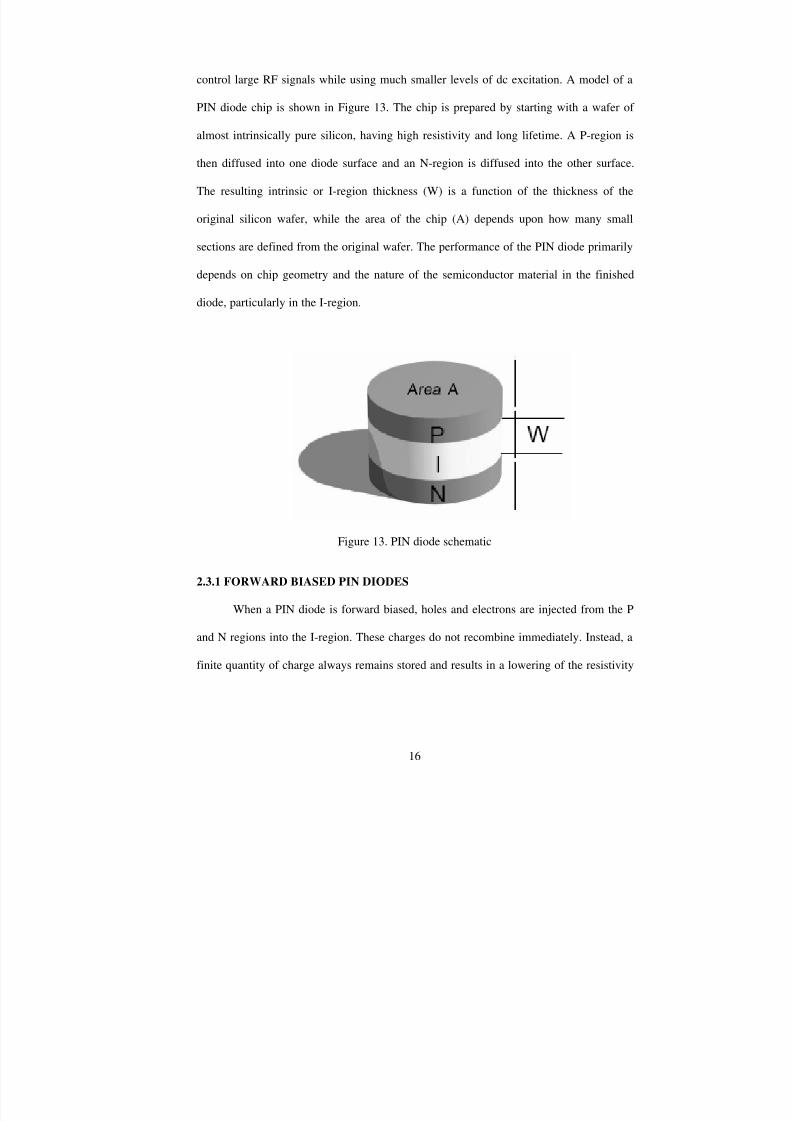
Figure 13: PIN diode schematic………………………………………………………... 16
Figure 14: Equivalent circuits for reverse and forward biased diode …………………. 18
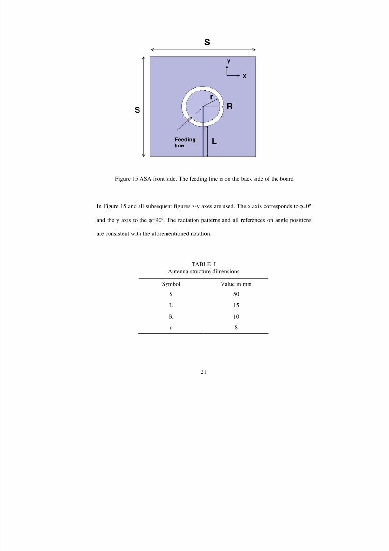
Figure 15: ASA front side. The feeding line is on the back side of the board ……….. 21
Figure 16: 3-D Radiation pattern of ASA without short along the circumference
The null is directed in the feeding line direction. (y- axis)…………………. 22
Figure 17: Eφ radiation pattern at 5.8 GHz for ASA without short …………………… 22
Figure 18: ASA matched at 5.2 GHz with 2 hard-wire stubs …………………………. 24
Figure 19: Simulated normalized radiation patterns on the x-y plane with a short
circuit at 225º. The null direction for the slot without any short would
be in the 90o
direction with respect to the plot labeling…………………….. 25
Figure 20: Simulated return loss with linear matching stubs…………………………... 25

8/9/2019 Nikolaou Symeon 200512 Mast
http://slidepdf.com/reader/full/nikolaou-symeon-200512-mast 9/79
ix
Figure 21: Annular Slot Antenna schematic The feeding line with the matching
stubs are on the bottom and the annular slot antenna is on the top sideof the substrate. The short is placed at φ=225º, else 45º far from the
feeding line………………………………………………………………….. 26
Figure 22: Linear matching stubs without tapered segment…………………………… 27
Figure 23: Matching stubs with tapered segments……………………………………... 28
Figure 24: Photograph of the back side of the frequency reconfigurable design. Two
ASI 8001 PIN diodes are observed connecting the matching stubs to the
feeding line. The dc bias lines are also visible……………………………… 28
Figure 25: Simulation and measurement are presented for the three different
frequencies. Simulation is presented in solid line and measurementis presented in dashed line…………………………………………………... 29
Figure 26: Photograph of the front side of the annular slot antenna. TwoMBP-1035-E28 PIN diodes are observed, soldered symmetrically 45
from the feeding line………………………………………………………... 30
Figure 27: ASA frequency reconfigurable design matching network…………………. 32
Figure 28: Small diode effect in the frequency reconfigurable design for the
5.2 GHz stub………………………………………………………………… 34
Figure 29: Diodes effect in return loss measurement for the 5.2 GHz design…………. 35
Figure 30: Diodes effect in return loss measurement for the 6.4 GHz design…………. 35
Figure 31: Fabricated samples. The short on the slot is implemented with a
hard-wired short or with a MBP-1035-E28 PIN diode……………………... 36
Figure 32: Fabricated matching stubs for 5.2 and 6.4 GHz……………………………. 36
Figure 33: E field distribution for unperturbed (no shorts) annular slot antenna……… 40
Figure 34: Electric field distribution for f=5.8 GHz when a short is placed at 225º.
The dipoles model is superimposed for comparison…………………………40
Figure 35: 3-D radiation pattern that presents a null in the feed line direction(y axis) for f=5.8 GHz ……………………………………………………… 41
Figure 36: 3-D radiation pattern that presents a null in the 45o
direction when ashort is used at 225 o along the slot circumference for f=5.8 GHz………….. 41
Figure 37: Simulated normalized radiation patterns on the x-y plane with a shortcircuit at 225º. The null direction for the slot without any short would
be in the 90o
direction with respect to the plot labeling…………………….. 42

8/9/2019 Nikolaou Symeon 200512 Mast
http://slidepdf.com/reader/full/nikolaou-symeon-200512-mast 10/79
x
Figure 38: Simulation and measurement results for the null reconfigurable design
The first two lines refer to the design without any short. The numbersin the label refer to the hard-wired short position compared to the
polar plot label in Figure 37………………………………………………... 43
Figure 39 : Magnetic dipoles model of ASA with short circuit at 225º. Three
dipoles are used in equilateral triangle orientation (Blue solidlines are for 5.8 GHz and green dotted lines for 5.2 GHz)………………… 44
Figure 40: Analytical expression plot of ASA with short circuit at 225º comparedto the numerical solution for the amplitude of E field …………………….. 45
Figure 41: Magnetic Current amplitude distribution along the annular slot…………… 46
Figure 42: Magnetic current phase distribution along the annular slot The 0corresponds to the short position. The singularity at 45o is due the
excitation source. The phases and normalized amplitudes correspond
to M2, M1 and M3 from left to the right…………………………………….. 46
Figure 43: Three dipoles in equilateral triangle orientation…………………………… 48
Figure 44: ASA Null reconfigurable design matching network……………………….. 50
Figure 45: Diodes effect in return loss measurement for the null reconfigurable
design. The design frequency was 5.8 GHz………………………………… 51
Figure 46: Photograph of the tested ASA with the rounded corners. The dc probes
for the diodes bias can be seen…………………………………………….. 53
Figure 47: Eφ radiation pattern at 5.8 GHz with the short along the slotcircumference……………………………………………………………….. 53
Figure 48: Measured radiation patterns for the design frequencies when a hard- wired
short is placed at 225o………………………………………………………. 54
Figure 49 : Radiation patterns for the 5.2 GHz frequency design when the short is
placed at 315o. Simulation, measurement with hard-wired short,
measurement with the big diode biased, and measurement with thesmall diode biased are presented……………………………………………. 55
Figure 50: Radiation patterns for the 6.4 GHz frequency design when the short isplaced at 225o. Simulation, measurement with hard-wired short,
measurement with the big diode biased, and measurement with
the small diode biased are presented………………………………………... 55
Figure 51: Simulated radiation patterns in x-y plane for the null reconfigurabledesign at f=5.8 GHz. The null is directed at 45o, 90o, and 135o direction.
The 90o direction is the null direction when no short is .….……………….. 57

8/9/2019 Nikolaou Symeon 200512 Mast
http://slidepdf.com/reader/full/nikolaou-symeon-200512-mast 11/79
xi
Figure 52 : Measured radiation patterns in x-y plane for the null reconfigurable
design at f=5.65 GHz. The null is directed at 45o, 90
o, and 135
o
direction using two PIN diodes placed at. 225o and 315o .The 90o direction is achieved when none of the diodes is biased……………………. 57

8/9/2019 Nikolaou Symeon 200512 Mast
http://slidepdf.com/reader/full/nikolaou-symeon-200512-mast 12/79
xii
LIST OF SYMBOLS AND ABBREVIATIONS
3-D Three Dimensional
ASA Annular Slot Antenna
GSM Global System of Mobile Communications
ISM Industrial-Scientific-Medical
MEMS Micro-Electro-Mechanical- Systems
PIN P-region I-region N-region
RF Radio Frequency
WLAN Wireless-Local-Area-Network

8/9/2019 Nikolaou Symeon 200512 Mast
http://slidepdf.com/reader/full/nikolaou-symeon-200512-mast 13/79
xiii
SUMMARY
The following document presents the design of a reconfigurable annular slot
antenna (ASA) for wireless communications and wireless local area network (WLAN)
applications. The multitude in different standards in cell phones and other personal
mobile devices require compact multi-band antennas and smart antennas with
reconfigurable features. The use of the same antenna for a number of different purposes,
preferably in different frequencies is highly desirable. The proposed design demonstrates
reconfigurability both in frequency and in radiation pattern. The operating frequencies are
5.2 GHz, 5.8 GHz and 6.4 GHz, and the radiation pattern is steered in three different
directions with the use of shorts along the slot circumference. The use of PIN diodes is
proposed to implement the switches that are used along the slot circumference, and with
the matching stubs.
The annular slot antenna consists of a circular slot on a square, metal ground
plane that is fed by a microstrip line, designed on the bottom of the Duroid substrate. The
mean length of the slot circumference is approximately 3λ s /2 at the frequency of 5.8 GHz
where λ s is the equivalent wavelength in a slot line with 2 mm width, which is the design
slot width. The microstrip feed line terminates in an open circuit that is approximately
λg /4 from the ring where λg is the wavelength on the microstrip line. At the intersection
of the microstrip line and the slot, magnetic coupling occurs, which, due to the 3λs /2 ring
circumference, creates a null in the radiation pattern in the direction of the microstrip
feed line. To change the direction of the null, short circuits have to be placed on the slot.
The proposed design directs the null in two additional directions forming +45o
and -45o

8/9/2019 Nikolaou Symeon 200512 Mast
http://slidepdf.com/reader/full/nikolaou-symeon-200512-mast 14/79
xiv
angles with the feeding line direction. For a non-reconfigurable design, these may be
hard-wired slotline short circuits, but in the reconfigurable design, they are implemented
with pin diodes. The short in the slot results in a reformation of the electric field
distribution along the slot leading to a shift of the null in the short direction. The
equivalent load at the input of the microstrip transmission line also changes when a short
exists on the slot compared to the case when no short exists; therefore, reconfigurable
matching stubs are required to keep the antenna matched at the design frequency. Linear
matching stubs are also used to match the antenna at different frequencies when the slot
configuration is kept constant. As a proof of concept, the antenna is designed to operate
at 5.2 and 6.4 GHz in addition to the initial frequency of 5.8 GHz. To reconfigure the
matching network, pin diodes are used to connect or disconnect the stubs from the
microstrip transmission line and consequently shift the resonance to the desired
frequency.
The proposed compact reconfigurable slot antenna may be used for IEEE802.11a
(5.8GHz) WLAN and other practical wireless communications systems, such as global
system of mobile communications (GSM) and Bluetooth Industrial-Scientific-Medical
(ISM) devices. Research was done to obtain a basic knowledge of annular slot and
reconfigurable antenna design over the past few years. Both analytical and numerical
methods are used to implement a realistic, functional and efficient design. Parametric
analyses using simulation tools are performed to study critical parameters that may affect
the designs. Finally, the simulated designs are fabricated, and measured results are
presented that validate the design approaches.

8/9/2019 Nikolaou Symeon 200512 Mast
http://slidepdf.com/reader/full/nikolaou-symeon-200512-mast 15/79
1
CHAPTER 1
INTRODUCTION
Antennas have been used in the past for both military and commercial
applications. The original use of antennas was confined primarily in communications
radio transceivers operating in the MHz range. The antennas for military applications
were used for radar systems and peer to peer communications between units. Most of
those antennas were bulky (Figure 1) and costly and therefore accessible to a small,
specialized category of people. In the last 20 years though, personal and mobile
communications networks have developed rapidly, causing an increasing need for
affordable, compact and easily integrated antennas. The increasing demand for cellular
phone services, wireless ι nternet access, wireless cable television, among others, will
force such systems to provide high throughput, and therefore very large bandwidths as
well as simultaneous access to different systems through the same device, which can be
accomplished with multi-band technology.
a. b.
Figure 1. (a.) circular horn, (b.) pyramidal horn.

8/9/2019 Nikolaou Symeon 200512 Mast
http://slidepdf.com/reader/full/nikolaou-symeon-200512-mast 16/79
2
As a result of the increasing need for gradually smaller and more affordable
antennas a lot of research has been going on. The major need for commercial antennas
concerns miniaturized planar antennas suitable for relatively small mobile devices like
cell phones or portable computers. Patch antennas (Figure 2), printed dipoles and slot
antennas fall into that category. A special type of slot antennas, annular slot antennas
(Figure 3) will be the focus of this research project.
Figure 2. Patch antenna.
Figure 3. Annular slot antenna on dielectric material.

8/9/2019 Nikolaou Symeon 200512 Mast
http://slidepdf.com/reader/full/nikolaou-symeon-200512-mast 17/79
3
The need of wide operation diversity forces wireless communications systems to use
different high frequency bands in the microwave and millimeter wave regions; frequency
bands in which slot antennas are often used. However, slot antennas have limited
bandwidth problems and not many bandwidth control techniques have been published.
An additional problem is the existence of many mobile users who probably use the same
operation frequency. Therefore their signal becomes an undesired interferer for a
neighboring user. So a technique is needed to potentially reject the interference from a
certain direction. If the blockage of such a signal is impossible then the interested user
has to immune his receiver to the received signal. This can be done by directing a
radiation pattern null in that direction and consequently blinding the receiver in that
direction. This can be done using a reconfigurable radiation pattern antenna that enables
the user to turn the radiation pattern in the desired direction in a similar concept that radar
phased arrays direct the narrow main beam to an electronically controlled direction.
Apparently the need for a reconfigurable radiation pattern antenna and a multi
frequency antenna is obvious. An antenna design with a combination of those two
reconfigurability characteristics would be highly desired. This research focuses on a
technique to control the radiation pattern and at the same time maintain a multi frequency
operation for a single low profile, low cost antenna. An annular slot antenna loaded with
PIN diodes along its circumference is proposed for this purpose. The planar antenna is
fabricated on one side of a Duroid substrate and the microstrip feeding line with the
matching network is fabricated on the opposite side of the board. The central frequency is
5.8 GHz and, by reconfiguring the matching circuit, the antenna was also designed to
operate at 5.2 GHz and 6.4 GHz. Pin diodes are also used to short the ASA in pre-

8/9/2019 Nikolaou Symeon 200512 Mast
http://slidepdf.com/reader/full/nikolaou-symeon-200512-mast 18/79
4
selected positions along the circumference, thereby changing the direction of the null in
the plane defined by the circular slot changes. As a proof of concept, two pin diodes are
placed 45 º on both sides of the feeding line along the ASA and the direction of the null is
shown to align with the direction defined by the circular slot center and the diode.
Consequently a design that is reconfigurable in both frequency and radiation pattern is
accomplished. The antenna was designed using Ansoft HFSS simulator and was
fabricated in Georgia Tech facilities. The fabricated prototypes were tested and measured
and their results are compared with the simulated results. Return loss and radiation
pattern measurements and simulations are presented, which are in very good agreement.
Basic theory about slot antennas and annular slot antennas is presented in Chapter 2 along
with the approaches followed by other people and reported in literature. In Chapter 3 the
frequency reconfigurable design, the design and optimization of linear matching stubs
and their integration with PIN diodes are discussed. The radiation pattern reconfigurable
design and an accurate model that discusses the null rotation are presented in Chapter 4.
Finally, Chapter 5 presents conclusions and potential applications for the proposed
antenna design.

8/9/2019 Nikolaou Symeon 200512 Mast
http://slidepdf.com/reader/full/nikolaou-symeon-200512-mast 19/79
5
CHAPTER 2
BACKGROUND
The slot antennas have the advantage of being able to produce bidirectional
radiation patterns with higher bandwidth, compared to patch antennas. In addition
antennas with desired polarization can be produced by using a combination of strip
conductors and slots arranged along the sides of a mictrostrip feed. The operation
principles and the antenna characteristics of slot antennas are shortly discussed in this
chapter. The basic element of the rectangular slot is presented at first, and the issues
evolved from the microstip feeding are presented. Based on the concepts already
discussed about the microstrip fed rectangular slot, the microstrip fed annular slot and the
loaded annular slot are introduced. In the second section, the work done by other people
on multi band and reconfigurable slot antennas is noted. Finally some information about
pin diodes which implement the switches for the reconfigurable antenna is provided.
2.1 MICROSTRIP-FED RECTANGULAR AND ANNULAR SLOT ANTENNAS
2.1.1 RECTANGULAR SLOT
A microstrip slot antenna comprises a slot cut in the ground plane of the micostrip
line such that the slot is perpendicular to the strip conductor of the microstrip line. The
slot is excited by the fields of the microstrip line. For efficient excitation of the slot, the
strip conductor is terminated in an open-circuited stub beyond the edge of the slot as
shown in Figure 4. Alternatively the strip conductor can be short-circuited

8/9/2019 Nikolaou Symeon 200512 Mast
http://slidepdf.com/reader/full/nikolaou-symeon-200512-mast 20/79
6
Ground Plane
Radiation Slot
Micropstrip
LineLm
DielectricSubstrate
Ground Plane
Radiation Slot
Micropstrip
LineLm
DielectricSubstrate
Figure 4. Microstrip fed rectangular slot antenna
through the dielectric substrate to the edge of the slot but this second technique is more
difficult to fabricate. The length Lm of the open-circuited microstrip stub is
approximately a quarter wavelength long so that an effective short circuit is realized at
the outer edge of the slot as shown in Figure 4. A center-fed slot antenna has a very high
radiation resistance, therefore in order to match the antenna to the characteristic
impedance of the microstrip line a matching network needs to be used.
There are three ways to reduce the resistance seen by the feed line for a given slot
size. The first is off-center feeding as suggested in [1]. The second is stub tuning as
suggested by Pozar in [2]. This technique is similar to the technique in Figure 4 except
that the length Lm of the microstrip stub is longer than a quarter wavelength. The stub
tuning introduces a reactive loading on the antenna that changes the resonant frequency.
The stub is designed so that the input resistance compares with the feed line impedance at
the new resonance frequency. The third feeding option is that the slot is center fed but
8/9/2019 Nikolaou Symeon 200512 Mast
http://slidepdf.com/reader/full/nikolaou-symeon-200512-mast 21/79
7
forms an angle with the feed slot. Consequently the slot is not perpendicular to the feed
line. The slot antenna has the advantage of low cross-polarization as compared to the
microstrip patch antennas [3]. It is normally bidirectional but can become unidirectional
by using a metallic cavity or a metallic reflector in the back side. The microstrip-fed has
been studied by many researchers both theoretically and experimentally. Some
approximate network models have also been proposed to design the antenna efficiently.
For additional information the reader can refer to [4].
The rectangular slots are considered to be the dual equivalent to linear wire
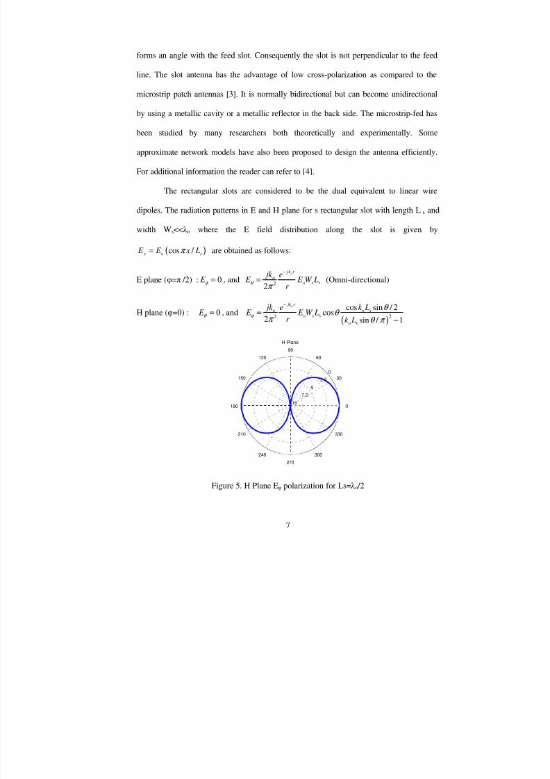
dipoles. The radiation patterns in E and H plane for s rectangular slot with length Ls and
width Ws<<λ ο where the E field distribution along the slot is given by
( )cos / y o s E E x Lπ = are obtained as follows:
E plane (φ=π /2) : 0 E φ = , and2
2
o jk r
oo s s
jk e E E W L
r θ
π
−
= (Omni-directional)
H plane (φ=0) : 0 E θ = , and
( )22
cos sin / 2cos
2 sin / 1
o jk r
o o so s s
o s
jk e k L E E W L
r k L
φ
θ θ
π θ π
−
=
−
0
-2.5
-5
-7.5
-100
30
60
90
120
150
180
210
240
270
300
330
H Plane
Figure 5. H Plane Eφ polarization for Ls=λ ο /2
8/9/2019 Nikolaou Symeon 200512 Mast
http://slidepdf.com/reader/full/nikolaou-symeon-200512-mast 22/79
8
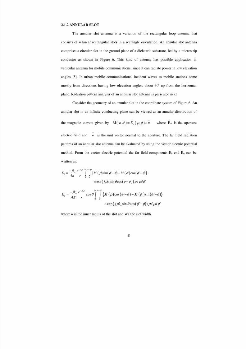
2.1.2 ANNULAR SLOT
The annular slot antenna is a variation of the rectangular loop antenna that
consists of 4 linear rectangular slots in a rectangle orientation. An annular slot antenna
comprises a circular slot in the ground plane of a dielectric substrate, fed by a microstrip
conductor as shown in Figure 6. This kind of antenna has possible application in
vehicular antenna for mobile communications, since it can radiate power in low elevation
angles [5]. In urban mobile communications, incident waves to mobile stations come
mostly from directions having low elevation angles, about 30o
up from the horizontal
plane. Radiation pattern analysis of an annular slot antenna is presented next
Consider the geometry of an annular slot in the coordinate system of Figure 6. An
annular slot in an infinite conducting plane can be viewed as an annular distribution of
the magnetic current given by ( ) ( ), ' , 'a E n ρ φ ρ φ → → ∧
Μ = × where α
→
Ε is the aperture
electric field and n∧
is the unit vector normal to the aperture. The far field radiation
patterns of an annular slot antenna can be evaluated by using the vector electric potential
method. From the vector electric potential the far field components E θ end Eφ can be
written as:
( ) ( ) ( ) ( ){ }
( )( )
2
0
sin ' ' cos '4
exp sin cos '
oWs jk r
o
o
jk e E M M
r
j k ΄ d d
π α
θ
α
ρ φ φ φ φ φ π
ρ θ φ φ ρ ρ φ
+−−= − + −
× −
∫ ∫
( ) ( ) ( ) ( ){ }
( )( )
2
0
cos cos ' ' sin '4
exp sin cos ' '
o
Ws jk r
o
o
jk e E M M r
j k d d
π α
φ
α
θ ρ φ φ φ φ φ π
ρ θ φ φ ρ ρ φ
+−
−= − − −
× −
∫ ∫
where α is the inner radius of the slot and Ws the slot width.

8/9/2019 Nikolaou Symeon 200512 Mast
http://slidepdf.com/reader/full/nikolaou-symeon-200512-mast 23/79
9
Figure 6. Microstrip fed annular slot
( ) ( ) ( ), ' ' φ ρ ρ φ ρ ρ φ φ ρ φ → → ∧ → ∧ → ∧ → ∧
Μ = Μ + Μ = − Ε + Ε
Eρ and Eφ are the slot field components in the ρ and φ directions, respectively. When the
slot width Ws<<λ o is small enough one can assume that Eφ=0. With this assumption and
after the integration with respect to φ the electric far field expressions become:
( )cos ' sin2
o jk r n o s
o n o
k W e E j E n J ak
r θ α φ θ
−
= −
( )sin cot sin2
o jk r n s
o n o
W e E j nE n J ak
r φ φ θ θ
−
=
n J and '
n J are the Bessel function of order n and it’s derivative respectively. The plots of
E field in planes E and H, when n=0 and n=1 are presented in Figures 7-9.

8/9/2019 Nikolaou Symeon 200512 Mast
http://slidepdf.com/reader/full/nikolaou-symeon-200512-mast 24/79
10
Figure 7. Radiation patterns of annular slots when n=0 and Ws<<λ ο [4]
Figure 8 Eplane radiation patterns of annular slots when n=1 and Ws<<λ ο [4]

8/9/2019 Nikolaou Symeon 200512 Mast
http://slidepdf.com/reader/full/nikolaou-symeon-200512-mast 25/79
11
Figure 9. E plane radiation patterns of annular slots when n=1 and Ws<<λ ο [4]
Circular polarization can be realized by feeding it such that two modes with
orthogonal polarizations, equal amplitude, and 90o
phase difference are excited. For this
purpose one can choose between a single feed design with a power splitter and a dual
feed design. Circular polarization can be achieved by loading the slot with a short along
the circular circumference. The loaded antenna has been studied by Morishita et al. [5].
The antenna characteristics such as input impedance, resonance frequency, bandwidth,
radiation pattern and polarization have been studied as a function of the position of the
short in the slot aperture. It has been shown that the resonant frequency can be varied by
changing the shorting position. Additionally the radiation patterns can be varied.

8/9/2019 Nikolaou Symeon 200512 Mast
http://slidepdf.com/reader/full/nikolaou-symeon-200512-mast 26/79
12
2.2 PAST TECHNIQUES AND APPROACHES
The multitude of different standards in cell phones and other personal mobile
devices require compact multi-band antennas and smart antennas with reconfigurable
features. The use of the same antenna for a number of different purposes, preferably in
different frequencies is highly desirable. A number of different reconfigurable antennas,
planar and 3-D have been developed. Some of them were developed for radar
applications [6]-[7] and other planar antennas were designed for wireless devices [8]-[9].
Reconfigurable patch antennas were also designed to operate in both L and X bands [10].
Most of those papers demonstrate only frequency reconfigurability. The reconfigurable
Annular Slot Antenna (ASA) proposed for this project operates at three frequencies with
the central frequency at 5.8 GHz, and it also has a reconfigurable radiation pattern. It will
be fabricated on low cost material and is a compact design suitable for integrating in
mobile systems. The annular slot antenna on dielectric material has been described
explicitly in [5]. The effect of one shorted point along the circumference has been
explored in [7], and an application of a shorted ASA integrated with a narrowband filter
is presented in [12], while the effect of capacitive loading is investigated in [13]. While
the literature concerning the shorted ASA is limited, a significant number of papers have
been published investigating feeding techniques and several antenna features like the
input impedance, the radiation efficiency, and the radiation pattern of a pure ASA. For
the antenna feature analysis, both analytical [14], [15] and numerical techniques [16]
were used and different approaches or models were applied [17]. Various feeding lines
[18] and feeding techniques are used in order to achieve broader bandwidth, or to
demonstrate multi-band operation [19] – [24]. In these designs all resonating frequencies
8/9/2019 Nikolaou Symeon 200512 Mast
http://slidepdf.com/reader/full/nikolaou-symeon-200512-mast 27/79
13
are excited simultaneously.
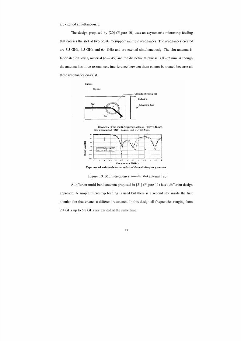
The design proposed by [20] (Figure 10) uses an asymmetric microstrip feeding
that crosses the slot at two points to support multiple resonances. The resonances created
are 3.5 GHz, 4.5 GHz and 6.4 GHz and are excited simultaneously. The slot antenna is
fabricated on low εr material (εr=2.45) and the dielectric thickness is 0.762 mm. Although
the antenna has three resonances, interference between them cannot be treated because all
three resonances co-exist.
Figure 10. Multi-frequency annular slot antenna [20]
A different multi-band antenna proposed in [21] (Figure 11) has a different design
approach. A simple microstrip feeding is used but there is a second slot inside the first
annular slot that creates a different resonance. In this design all frequencies ranging from
2.4 GHz up to 6.8 GHz are excited at the same time.
8/9/2019 Nikolaou Symeon 200512 Mast
http://slidepdf.com/reader/full/nikolaou-symeon-200512-mast 28/79
14
Figure 11. Multi-band annular slot antenna [21]
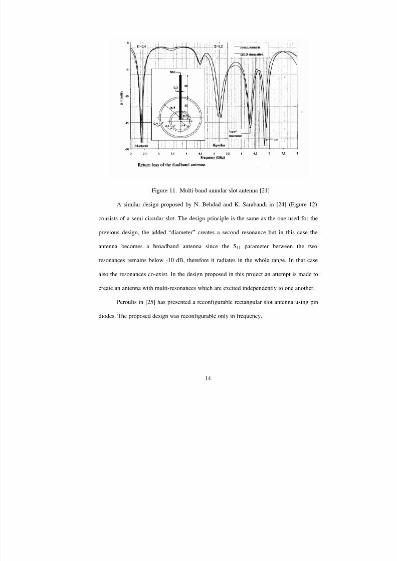
A similar design proposed by N. Behdad and K. Sarabandi in [24] (Figure 12)
consists of a semi-circular slot. The design principle is the same as the one used for the
previous design, the added “diameter” creates a second resonance but in this case the
antenna becomes a broadband antenna since the S11 parameter between the two
resonances remains below -10 dB, therefore it radiates in the whole range. In that case
also the resonances co-exist. In the design proposed in this project an attempt is made to
create an antenna with multi-resonances which are excited independently to one another.
Peroulis in [25] has presented a reconfigurable rectangular slot antenna using pin
diodes. The proposed design was reconfigurable only in frequency.

8/9/2019 Nikolaou Symeon 200512 Mast
http://slidepdf.com/reader/full/nikolaou-symeon-200512-mast 29/79
15
Figure 12. Semi-circular slot antenna [24]
While the radiation pattern is an essential parameter of an antenna, very little has
been published about radiation pattern control techniques for the ASA [26].
In this project, we present for first time an annular slot antenna with simultaneous
frequency and radiation pattern reconfigurability, by using pin diodes to short the ASA at
pre-determined locations, and to reconfigure the matching circuit. For this antenna only
one frequency resonates at a time, which is desirable when there are power or
interference issues.
2.3 PIN DIODES
A PIN diode is a semiconductor device that operates as a variable resistor at RF
and microwave frequencies. The resistance value of the PIN diode is determined only by
the forward biased dc current. In switch and attenuator applications, the PIN diode should
ideally control the RF signal level without introducing distortion which might change the
shape of the RF signal. An important additional feature of the PIN diode is its ability to
8/9/2019 Nikolaou Symeon 200512 Mast
http://slidepdf.com/reader/full/nikolaou-symeon-200512-mast 30/79
16
control large RF signals while using much smaller levels of dc excitation. A model of a
PIN diode chip is shown in Figure 13. The chip is prepared by starting with a wafer of
almost intrinsically pure silicon, having high resistivity and long lifetime. A P-region is
then diffused into one diode surface and an N-region is diffused into the other surface.
The resulting intrinsic or I-region thickness (W) is a function of the thickness of the
original silicon wafer, while the area of the chip (A) depends upon how many small
sections are defined from the original wafer. The performance of the PIN diode primarily
depends on chip geometry and the nature of the semiconductor material in the finished
diode, particularly in the I-region.
Figure 13. PIN diode schematic
2.3.1 FORWARD BIASED PIN DIODES
When a PIN diode is forward biased, holes and electrons are injected from the P
and N regions into the I-region. These charges do not recombine immediately. Instead, a
finite quantity of charge always remains stored and results in a lowering of the resistivity

8/9/2019 Nikolaou Symeon 200512 Mast
http://slidepdf.com/reader/full/nikolaou-symeon-200512-mast 31/79
17
of the I-region. The quantity of stored charge, Q, depends on the recombination time, τ
(the carrier lifetime), and the forward bias current, IF, as follows:
f Q I τ = [Coulomb] The resistance of the I-region under forward bias, Rs is inversely
proportional to Q and may be expressed as( )
2
S
N P
W R
Q µ µ =
+ [Ohms] where: W = I-
region width, µN = electron mobility, µΡ = hole mobility
Combining those equations, the expression for RS as an inverse function of current is
shown as( )
2
S
N P f
W R
Q µ µ τ =
+ Ι. This equation is independent of area. In the real world
the RS is slightly dependent upon area because the effective lifetime varies with area and
thickness due to edge recombination effects.
2.3.2 REVERSE BIASED PIN DIODES
At high RF frequencies when a PIN diode is at zero or reverse bias, it appears as a
parallel plate capacitor, essentially independent of reverse voltage, having a value of:
C W
ε Α= [Farads] where: ε = silicon dielectric constant, A = junction area W = I-region
thickness. The lowest frequencies at which this effect begins to predominate are related
to the dielectric relaxation frequency of the I-region, f t, which may be computed:
2 f τ
πρε
Ι= where: ρ = I-region resistivity.
At frequencies much lower than f τ the capacitance characteristic of the PIN diode
resembles a varactor diode. Because of the frequency limitations of common test
equipment, capacitance measurements are generally made at 1 MHz. At this frequency
the total capacitance, CΤ, is determined by applying a sufficiently large reverse voltage

8/9/2019 Nikolaou Symeon 200512 Mast
http://slidepdf.com/reader/full/nikolaou-symeon-200512-mast 32/79
18
which fully depletes the I-region of carriers. Associated with the diode capacitance is a
parallel resistance, Rp, which represents the net dissipative resistance in the reverse
biased diode. At low reverse voltages, the finite resistivity of the I-region results in a
lossy I-region capacitance. As the reverse voltage is increased, carriers are depleted from
the I-region resulting in an essentially lossless silicon capacitor. The reverse parallel
resistance of the PIN diode, Rp, is also affected by any series resistance in the
semiconductor or diode contacts. The equivalent circuits are presented in Figure 14. CΤ is
the total capacitance and L is the total package inductance.
Figure 14. Equivalent circuits for reverse and forward biased diode
2.4 SUMMARY
In this chapter, the necessary theoretical background to comprehend the design
parameters of the proposed reconfigurable ASA, has been presented. The radiation and
matching principles of rectangular and annular slots have been briefly discussed and the
suggested designs and applications by other researchers have been outlined. Finally the

8/9/2019 Nikolaou Symeon 200512 Mast
http://slidepdf.com/reader/full/nikolaou-symeon-200512-mast 33/79

8/9/2019 Nikolaou Symeon 200512 Mast
http://slidepdf.com/reader/full/nikolaou-symeon-200512-mast 34/79
20
CHAPTER 3
FREQUENCY RECONFIGURABLE DESIGN
The annular slot antenna has been shown to demonstrate high radiation efficiency
in a wide range of frequencies. In several examples demonstrated in the previous chapter
the microstrip fed annular slot has presented multi frequency behavior. The drawback in
those designs is that the radiating resonances appear simultaneously and in indigenous
non pre-selected frequencies. An example would be a harmonic resonance that appears as
a result of the structure and not as a result of a design methodology. In this chapter the
use of linear matching stubs is proposed to match the antenna in pre-selected frequencies.
The matching stubs are connected to the microstrip feeding line using PIN diodes as
switches.
3.1 ANTENNA STRUCTURE
The annular slot antenna consists of a circular slot on a square, metal ground
plane that is fed by a microstrip line fabricated on the opposite side of the substrate as can
be seen in Figure 15. The design parameters are summarized in Table 1. The mean length
of the slot circumference is approximately 3λ s /2 at the design frequency where λ s is the
equivalent wavelength in a slot transmission line with slot width w=R-r, which is small
compared to λ s. The microstrip feed line terminates in an open circuit that is
approximately λ g /4 from the ring where λ g is the guided wavelength on the microstrip
line. At the intersection of the microstrip line and the slot, magnetic coupling occurs,
which, due to the 3λ s /2 ring circumference, creates a null in the radiation pattern in the
direction of the microstrip feed line. The 3-D pattern is presented in Figure 16 and the 2-
D Eφ polarization is presented in Figure 17.
8/9/2019 Nikolaou Symeon 200512 Mast
http://slidepdf.com/reader/full/nikolaou-symeon-200512-mast 35/79
21
R
r
Feedingline
S
S
L
R
r
Feedingline
S
S
L
X
y
Figure 15 ASA front side. The feeding line is on the back side of the board
In Figure 15 and all subsequent figures x-y axes are used. The x axis corresponds to φ=0º
and the y axis to the φ=90º. The radiation patterns and all references on angle positions
are consistent with the aforementioned notation.
TABLE I
Antenna structure dimensions
Symbol Value in mm
S 50
L 15
R 10
r 8

8/9/2019 Nikolaou Symeon 200512 Mast
http://slidepdf.com/reader/full/nikolaou-symeon-200512-mast 36/79
22
Figure 16. 3-D Radiation pattern of ASA without short along the circumference The null
is directed in the feeding line direction. (y- axis)
Figure 17. Eφ radiation pattern at 5.8 GHz for ASA without short

8/9/2019 Nikolaou Symeon 200512 Mast
http://slidepdf.com/reader/full/nikolaou-symeon-200512-mast 37/79
23
The shorted slot is printed on the front side, and the feeding line with the
matching stubs, are printed on the back side of the board, using standard
photolithography. The antenna is fabricated on a 50 mm x 50 mm, 635 µm thick, low loss
(tanδ=0.0025) Rogers RO3006 with εr=6.15 and a copper thickness of 18 µm. The
antenna is fed by a 50 microstrip line with width of 0.92 mm and the matching stubs
are also 0.92 mm wide. The slot has an outer radius R=10 mm and inner radius 8 mm
resulting a slot width of 2 mm. The feeding line is 25 mm long and the end of the line is
at the slot center.
3.2 DESIGN METHODOLOGY
The ASA using various feeding techniques has been shown to have a relatively
wide bandwidth compared to a patch or other narrowband antennas [27]-[28]. For the
design dimensions used in this project, simulations predict radiation efficiency greater
than 80% over the frequency range from 4.8 GHz to 6.5 GHz. Since the radiating element
can radiate over a wide range, the matching network must also support a broad
bandwidth. Moreover, the use of diodes to create shorts in the annular ring for null
reconfiguration also affects the input impedance, and this also must be accounted for in
the matching circuit. The following technique was experimentally tested for the shorted
ASA. Instead of a broadband matching network, a reconfigurable matching network
employing stub tuners was designed to support three narrowband frequency ranges. At
the center frequency of 5.8 GHz, the input admittance was determined from the
simulations, and this admittance was transferred along the 50 microstrip line to the
point where the admittance had a real part of 0.02 siemens (=1/50 siemens) and a random
imaginary part. At that point, an open circuit microstrip stub was placed parallel to the

8/9/2019 Nikolaou Symeon 200512 Mast
http://slidepdf.com/reader/full/nikolaou-symeon-200512-mast 38/79
24
transmission line to cancel the imaginary part. For the case under study with the hard-
wired short at 45o
the required stub to match the ASA should be put 7.23 mm far from the
board edge and should have length equal to 4.21 mm (Figure 18). For the calculation of
the exact position and length of the matching stubs a code in Matlab was deeloped. For
the other frequencies, the impedance at the port needs to be determined with the first
matching stub in place so the other two frequencies are matched using the combination of
two stubs for each one of them. That means that with stub L2 connected to the microstrip
line, the new impedance at the port is used to define the position (D1=5.49mm) of the
second stub L1=4.98 mm to match the ASA at 5.2 GHz. Those additional stubs have
been shown not to affect in any way the radiation pattern. For the experimentally tested
case the short on the slot is placed at 45º from the feeding line, namely at 225o
as can be
seen in Figure 19. Because of symmetry, the same matching stubs can be used when the
short is placed at the symmetrical position 45º towards the opposite direction, which is at
315o.
Figure 18. ASA matched at 5.2 GHz with 2 hard-wire stubs
8/9/2019 Nikolaou Symeon 200512 Mast
http://slidepdf.com/reader/full/nikolaou-symeon-200512-mast 39/79
25
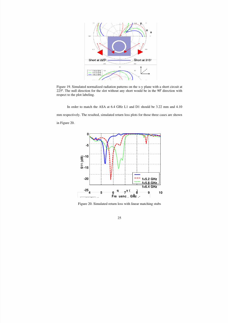
Short at 225o Short at 315o
x
y
φ
Short at 225o Short at 315oShort at 225o Short at 315o
x
y
φ
Figure 19. Simulated normalized radiation patterns on the x-y plane with a short circuit at
225º. The null direction for the slot without any short would be in the 90o direction with
respect to the plot labeling.
In order to match the ASA at 6.4 GHz L1 and D1 should be 3.22 mm and 4.10
mm respectively. The resulted, simulated return loss plots for those three cases are shown
in Figure 20.
4 5 6 7 8 9 10-25
-20
-15
-10
-5
0
Fre uenc GHz
S 1 1 ( d B )
f=5.2 GHzf=5.8 GHzf=6.4 GHz
Figure 20. Simulated return loss with linear matching stubs

8/9/2019 Nikolaou Symeon 200512 Mast
http://slidepdf.com/reader/full/nikolaou-symeon-200512-mast 40/79
26
The definition of the stubs length and position would be adequate if we wanted to
create three different antennas, one for each frequency since they seem to be matched
well as can be seen in Figure 20 from the three radiating resonances (below -10 dB) .
However in order to create a single reconfigurable design some additional tuning is
necessary. DC bias lines need to be added on the feeding line in order to provide a DC
path to forward and reverse bias the PIN diodes that are used. Although the bias lines are
very thin in order to be very resistive to the RF signal there is still some leakage that has
to be taken into consideration in order not to compensate the accuracy. Consequently the
aforementioned matching technique has to be repeated for a design than includes all three
stubs and the necessary bias lines (Figure 21).
S=50mm
S=50mm
r=8mm
R=10mm
L=15mm
45o
x
y
S=50mm
S=50mm
r=8mm
R=10mm
L=15mm
45o
x
y
Figure 21 Annular Slot Antenna schematic The feeding line with the matching stubs are
on the bottom and the annular slot antenna is on the top side of the substrate. The short is
placed at φ=225º, else 45º far from the feeding line

8/9/2019 Nikolaou Symeon 200512 Mast
http://slidepdf.com/reader/full/nikolaou-symeon-200512-mast 41/79
27
The diodes to be used are small compare to the stub width (0.92 mm) and as a
result a tapered segment is necessary in order to “match” the linear stub to the 200 µm
wide ASI 8001 PIN diodes. Therefore the length of the stubs needs to be redesigned in
order to meet the diode interface needs. The stubs schematic without the tapered
segments is presented in Figure 22. The stubs’ lengths for f=5.2 GHz and f= 6.4 GHz are
L’1=4.98 mm and L’2=3.22 mm respectively.
L’1=4.98
L’2=3.22
L’1=4.98
L’2=3.22
Figure 22. Linear matching stubs without tapered segment.
The addition of the tapered segments reduces the linear segment’s length. The diodes are
simulated as a perfect conductor with dimensions 200 µm x 200 µm. The linear segment
is simulated with Momentum ADS as a single port circuit and it’s characteristic S11 is set
as the goal for an equivalent stub (Figure 23) constituted from a small square part (diode
equivalent) the linear tapered part, and a linear part with a variable to be optimized
length. The linear part is 0.92 mm wide on the linear stub side and 200 µm wide on the

8/9/2019 Nikolaou Symeon 200512 Mast
http://slidepdf.com/reader/full/nikolaou-symeon-200512-mast 42/79
28
diode side. The optimized dimensions for the linear parts are L1=3.45 mm for the 5.2
GHz stub and
Linear Taper
Diode Equivalent
L1=3.45
L2=1.70
Linear Taper
Diode Equivalent
L1=3.45
L2=1.70
Figure 23. Matching stubs with tapered segments
L2=1.70 mm for the 6.4 GHz stub. A photograph of the fabricated prototype that shows
the soldered diodes on the taperd stubs is presented in Figure 24. The used ASI 8001 PIN
diodes will be referred to as “small” diodes.
Small Diode
Figure 24. Photograph of the back side of the frequency reconfigurable design. Two ASI
8001 PIN diodes are observed connecting the matching stubs to the feeding line. The dc
bias lines are also visible.

8/9/2019 Nikolaou Symeon 200512 Mast
http://slidepdf.com/reader/full/nikolaou-symeon-200512-mast 43/79
29
3.3 FREQUENCY RECONFIGURABLE DESIGN VALIDATION
In order to investigate the effect of the diodes, three different designs with the
correct matching network hard wired for each of the three frequencies were tested.
Simulations and measurements are in good agreement, (Figure 25) with a small shift
downwards for the 6.4 GHz resonance, which could be a result of fabrication inaccuracy
and imperfect connector soldering. In addition to the “small” diodes used for the
matching stubs two more MBP-1035-E28 PIN diodes are used to implement the switches
on the slot circumference. The MBP-1035-E28 PIN diodes will be referred to as “big”
diodes. The front side of the reconfigurable design with the diodes soldered on the slot is
presented in Figure 26.
4 5 6 7 8 9 10-25
-20
-15
-10
-5
0
Frequency (GHz)
S 1 1 ( d B )
f=5.2 GHzf=5.8 GHzf=6.4 GHz
Figure 25. Simulation and measurement are presented for the three different frequencies.
Simulation is presented in solid line and measurement is presented in dashed line

8/9/2019 Nikolaou Symeon 200512 Mast
http://slidepdf.com/reader/full/nikolaou-symeon-200512-mast 44/79
30
Big Diode
Figure 26. Photograph of the front side of the annular slot antenna. Two MBP-1035-E28
PIN diodes are observed, soldered symmetrically 45 from the feeding line.
The behavior of the diodes in both on and off state needs to be investigated. All
the cases for which forward biased diodes are supposed to be used, are compared with
hard-wire shorts. Therefore the suitable testing boards are fabricated and the performance
of the diodes is evaluated through the agreement between the return loss measurements
and the simulations. The comparison plots are presented in the following figures. For
those cases where two diodes need to be forward biased simultaneously, two boards are
fabricated and tested, substituting one diode at a time. The goal is to isolate the effect
from each diode and finally evaluate the performance of the combined use of “small” and
“big” diodes. The hard-wired boards are compared to the frequency reconfigurable
design that operates in all the aforementioned frequencies. A layout of the back side of
the antenna with the matching stubs designed as described in Section 3.2 is presented in
Figure 27. For shorting and opening the stubs to the feeding line, ASI 8001 PIN diodes

8/9/2019 Nikolaou Symeon 200512 Mast
http://slidepdf.com/reader/full/nikolaou-symeon-200512-mast 45/79
31
are used, which will be referred to as ‘small’ diodes. Their length is less than 200 µm. On
the annular slot, MBP-1035-E28 PIN diodes are used, which will be referred to as ‘big’
diodes. They are long enough to cover the 2 mm slot width. The matching network for
the frequency reconfigurable design with a “big” diode biased at 45º along the ASA is
shown in Figure 27. Three stubs of length L1, L3, and L2 are used to match the slot
antenna to 5.2, 5.8, and at 6.4 GHz respectively. The dc bias lines are used to apply the dc
voltage to the small diodes. When neither of the small diodes is biased, the antenna is
matched at 5.8 GHz, by forward biasing the diode on the stub of length L1, the antenna is
matched at 5.2 GHz, and by forward biasing the diode on the stub of length L2, the
antenna is matched to 6.4 GHz. The reconfigurable matching network dimensions are
presented in Table II.
In Figure 27 the 200 µm gaps (between the tapering small triangles and the
feeding line) for the small diodes can be seen. The radial stubs are 70º wide and all the
microstrip lines are 0.92 mm wide which results in a Zo of 50 . The thin feeding lines
are 120 µm wide and are used as dc bias lines. Their respective lengths are optimized for
the frequency used, so they are equivalent to an open for the RF signal while they are
perfect conductors for any applied dc current. The dc lines however are thin enough (very
high RF impedance) to prevent leakage for the frequencies for which they are not
optimized. Tapered segments are used to match the wider linear stubs to the small diodes
in order to minimize reflections. The design procedure and the optimization of the
matching stubs has been described in detail in section 3.2
8/9/2019 Nikolaou Symeon 200512 Mast
http://slidepdf.com/reader/full/nikolaou-symeon-200512-mast 46/79
32
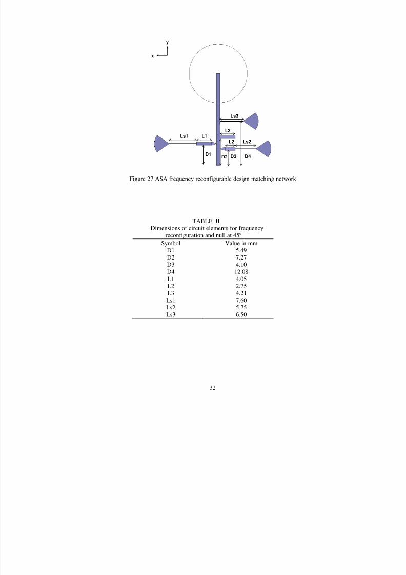
D1D2 D3 D4
Ls1 L1L3
L2 Ls2
Ls3
x
y
Figure 27 ASA frequency reconfigurable design matching network
TABLE II
Dimensions of circuit elements for frequency
reconfiguration and null at 45ºSymbol Value in mm
D1 5.49
D2 7.27
D3 4.10
D4 12.08
L1 4.05
L2 2.75
L3 4.21
Ls1 7.60
Ls2 5.75
Ls3 6.50

8/9/2019 Nikolaou Symeon 200512 Mast
http://slidepdf.com/reader/full/nikolaou-symeon-200512-mast 47/79
33
The antenna was fabricated on a 635 µm thick Rogers RO3006 substrate with
εr=6.15 and tanδ=0.0025. The antenna is fed by a 50 microstrip line. A standard
photolithography technique was used for fabrication. The copper thickness was 18 µm
and the alignment between the two copper layers was achieved by drilling holes on the
substrate using a laser method. Big and small diodes can be seen in Figure 24 and Figure
26, respectively. A current smaller than 10 mA, was used to forward bias the diodes. For
the small diode bias, dc bias lines were used and a wire carrying the bias was soldered to
the radial stub. For the big diodes, the ground plane was grounded and a wire was
soldered to the inner section of the ring. For return loss and radiation pattern
measurements a 3.5 mm SMA connector was soldered at the beginning of the feeding
line.
The small diodes are used to electrically connect the matching stubs to the
transmission line. When the diodes are soldered onto the board but are not biased, they
are equivalent to a small capacitive load. Their affect however is insignificant. That was
verified in both return loss measurements and radiation pattern measurements. Return
loss measurements to demonstrate the “small” diode effect are shown in Figure 28. When
the diode is biased, the circuit is designed to match at 5.2 GHz, which is close to the
measured resonant frequency in Figure 28. When the diode is not biased, the antenna is
designed to be matched at 5.8 GHz. The measurement with the diode not biased is
compared to the reference hardwired design of Figure 28 with no diodes on, and great
agreement is observed.
For the simulation, the forward biased diodes were modeled as conductors. The
small diode was modeled as a 0.2 mm x 0.25 mm 18µm thick Cu, and the big diode was

8/9/2019 Nikolaou Symeon 200512 Mast
http://slidepdf.com/reader/full/nikolaou-symeon-200512-mast 48/79
34
modeled as 2.2 mm x 1 mm perfect electric conductor. As a result the equivalent
capacitance that
4 5 6 7 8 9 10-30
-25
-20
-15
-10
-5
0
Frequency (GHz)
S 1 1 ( d B )
f=5.8 GHz DesignSmall Diode BiasedSmall Diode Not Biased
Figure 28. Small diode effect in the frequency reconfigurable design for the 5.2 GHz
stub
appears when the diode is forward biased was not taken into consideration for the
simulations and therefore a shift in the measured frequency appears compared to the
simulation results.
The small diodes have different and less significant effect on the return loss
compared to the effect of big diodes. The matching stub’s length is optimized to cancel
the imaginary part of the transmission line admittance at the resonance frequency. The
existence of a small capacitance because of the diode package modifies the input
imaginary part and consequently the length of the stub is no longer optimized for the
design frequency. The combination of the capacitance and the stub is optimal for a
“close” frequency and as a result, a small shift in the resonance frequency appears. The
effect of the diodes in the return loss for the 5.2 GHz design and the 6.4 GHz design are

8/9/2019 Nikolaou Symeon 200512 Mast
http://slidepdf.com/reader/full/nikolaou-symeon-200512-mast 49/79
35
presented in Figure 29 and Figure 30 respectively. Generally the presence of a diode
results in a shift of the resonance towards lower frequencies. Samples of the used
fabricated boards are presented in Figures 31 and 32.
4 5 6 7 8 9 10-30
-25
-20
-15
-10
-5
0
5
Frequency (GHz)
S 1 1 ( d B )
SimulationMeasurement(No diodes)Small Diode BiasedBig Diode Biased
Figure 29. Diodes effect in return loss measurement for the 5.2 GHz design
4 5 6 7 8 9 10-30
-25
-20
-15
-10
-5
0
Frequency (GHz)
S 1 1 ( d B )
SimulationMeas.(No Diodes)Small Diode BiasedBig Diode Biased
Figure 30. Diodes effect in return loss measurement for the 6.4 GHz design

8/9/2019 Nikolaou Symeon 200512 Mast
http://slidepdf.com/reader/full/nikolaou-symeon-200512-mast 50/79
36
Figure 31. Fabricated samples The short on the slot is implemented with a hard-wired
short or with a MBP-1035-E28 PIN diode
Figure 32. Fabricated matching stubs for 5.2 and 6.4 GHz

8/9/2019 Nikolaou Symeon 200512 Mast
http://slidepdf.com/reader/full/nikolaou-symeon-200512-mast 51/79
37
3.4 SUMMARY
In this chapter the proposed antenna structure with reconfigurable frequency has
been analyzed. The slot presented is the shorted annular slot that has a null at 45o
direction with respect to the feed line direction. To match the antenna at three different
frequencies linear matching stubs were used. PIN diodes were used for switches. The
integration of the linear matching stubs with the diodes and the performance
optimizations have been analytically described. The proposed design has been fabricated
and tested, and return loss measurements results have shown very good agreement with
the simulations. The effect of diodes on the return loss has been investigated and has
proved to be minor. Therefore the effectiveness of the pin diode as a switch and the
validity and accuracy of the simulated design have been verified. The behavior of the
ASA and the effect of diodes for the pattern reconfigurable design will be presented
and discussed in the next chapter.

8/9/2019 Nikolaou Symeon 200512 Mast
http://slidepdf.com/reader/full/nikolaou-symeon-200512-mast 52/79
38
CHAPTER 4
RADIATION PATTERN RECONFIGURABLE DESIGN
The pattern reconfigurability is a property highly desired for smart antennas. In
this chapter the idea of rotating the null direction of the ASA radiation pattern is
discussed. To change the direction of the null, pin diodes are used to create short circuits
across the slot. Generally a null appears opposite to the position where the short is placed,
but the short position must be tuned to compensate for discontinuity in the slot fields
caused by the feed line to achieve the desired null direction with accuracy. The
simulation results indicate that a null can be created anywhere between 15 o and 165o by
adding a short in the opposite direction. For a non-reconfigurable design, the short
circuits may be hard-wired slotline short circuits, but in the reconfigurable design, they
are implemented with pin diodes. The short in the slot results in a reformation of the
electric field distribution along the slot leading to a shift of the null in the short direction.
It also changes the equivalent load at the input of the microstrip transmission line;
therefore, reconfigurable matching stubs are required to keep the antenna matched at the
design frequency during null reconfiguration. To explain the null position, and the shift
in null position that is observed when the mean slot circumference is perturbed from the
3λ s /2 length, a simple but accurate theoretical model is proposed. The analytical
expressions deduced by the three magnetic dipoles that consist the model, are verified by
the numerical solution and the measurements. The proposed design is fabricated and
tested. In order to demonstrate the pattern reconfigurability the central frequency f=5.8
GHz is selected. The resonance frequency is maintained constant while the null shifts in
three positions. Return loss measurements and radiation pattern measurements are
presented that verify the model validity and demonstrate the design’s agility.

8/9/2019 Nikolaou Symeon 200512 Mast
http://slidepdf.com/reader/full/nikolaou-symeon-200512-mast 53/79
39
4.1 THEORETICAL ANALYSIS
4.1.1 PATTERN RECONFIGURABLE PRINCIPLES
The radiation patterns of the shorted ASA yield a null in a direction different than
the feeding line direction, which is the case for the regular, unperturbed slot. The E field
distribution along the slot for the unperturbed slot is presented in Figure 33 while the E
field distribution for the shorted slot is presented in Figure 34. It is obvious from the field
distribution plot that the field pattern and consequently the far field radiation pattern is
rotated by 45o. The simulated 3-D radiation patterns are presented in Figure 35 and
Figure 36 for the unperturbed and shorted ASA respectively. All the simulations
presented so far involve the 5.8 GHz frequency. The simulated x-y plane radiation
patterns for the case of a hard-wired short circuit at 225º are presented in Figure 37. In
Figure 37 and all subsequent figures x-y axes are used. The x axis corresponds to φ=0º
and the y axis to the φ=90º. The radiation patterns and all references on angle positions
are consistent with the aforementioned notation. In that plane the E field is polarized in φ
direction, parallel to the slot plane. The null is created in the x-y plane instead of the
broadside direction because it is meant to decrease the effect of an interferer coming from
a direction different than the directivity (maximum field value) direction, which is
parallel to z axis. At 5.8 GHz, for which the slot dimensions are optimized, a null exists
exactly opposite to the slot short with respect to the slot center. At 6.4 GHz, the null
appears approximately 10º closer to the 90o direction, while at 5.2 GHz, the null deviates
from the 90o
direction and moves closer to the 0o
direction by 5º.
Similarly, placing a
short circuit at 315º, results in a null in the radiation pattern at 135º for 5.8 GHz. As a
more general concept, when a frequency lower than the design frequency is used, the null

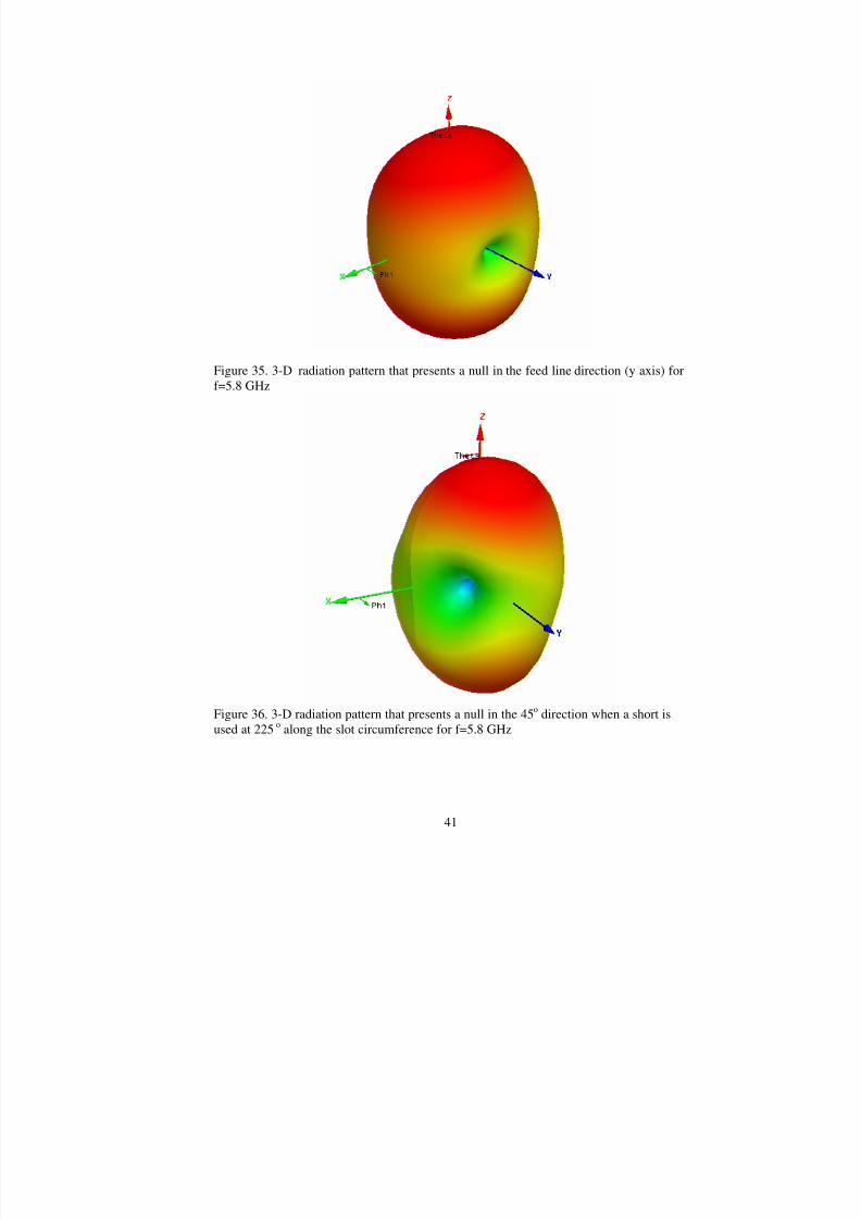
8/9/2019 Nikolaou Symeon 200512 Mast
http://slidepdf.com/reader/full/nikolaou-symeon-200512-mast 54/79
40
shifts towards the φ=90o
direction while it shifts towards the φ=0º direction when a
higher frequency than the design frequency is used.
Figure 33. E field distribution for unperturbed (no shorts) annular slot antenna
x
y
x
y
Figure 34. Electric field distribution for f=5.8 GHz when a short is placed at 225º. The
dipoles model is superimposed for comparison
8/9/2019 Nikolaou Symeon 200512 Mast
http://slidepdf.com/reader/full/nikolaou-symeon-200512-mast 55/79
41
Figure 35. 3-D radiation pattern that presents a null in the feed line direction (y axis) for
f=5.8 GHz
Figure 36. 3-D radiation pattern that presents a null in the 45o
direction when a short is
used at 225o
along the slot circumference for f=5.8 GHz

8/9/2019 Nikolaou Symeon 200512 Mast
http://slidepdf.com/reader/full/nikolaou-symeon-200512-mast 56/79
42
Short at 225o
x
y
φx
y
φ
Short at 225oShort at 225o
x
y
φx
y
φx
y
φ
Short at 225o
Figure 37. Simulated normalized radiation patterns on the x-y plane with a short circuit
at 225º. The null direction for the slot without any short would be in the 90o
direction
with respect to the plot labeling.
As discussed, varying the null position changes the impedance of the antenna and
requires a reconfigurable matching circuit. When a short is placed at 45º from the feeding
line, as shown in Figure 37, a single stub with length 4.21 mm and width 0.92 mm at a
distance of 7.27 mm from the feeding point is used to match this short position at 5.8
GHz. The exact layout for the null reconfigurable design will be discussed in detail in the
next section. When the short is removed, simulating the case that the diode is not biased,
a second stub must be added as a shunt matching device at the feeding line in order that
the resonance frequency remains constant. The technique to define the stubs’ length and
their position is explained in chapter 3. Return loss simulation and measurements are
presented in Figure 38, where it is seen that a 5.8 GHz resonant frequency is maintained

8/9/2019 Nikolaou Symeon 200512 Mast
http://slidepdf.com/reader/full/nikolaou-symeon-200512-mast 57/79
43
regardless whether or not a short exists. The 4.5 GHz parasitic resonance, when no short
circuits occur on the ring, is easily removed by filtering it with a microstrip passband
filter that can be cascaded to the antenna geometry.
4 5 6 7 8 9 10-30
-25
-20
-15
-10
-5
0
Frequency (GHz)
S 1 1 ( d B )
Simulation No ShortsMeasurement No ShortsSimulation Short at 225Measurement Short at 225
Figure 38. Simulation and measurement results for the null reconfigurable design Thefirst two lines refer to the design without any short. The numbers in the label refer to the
hard-wired short position compared to the polar plot label in Figure 37.
4.1.2 THREE DIPOLES MODEL
To qualitatively explain the shift in the null direction when a short is placed along
the slot, a novel but simple model using magnetic dipoles is introduced and briefly
discussed. The field distribution as a result of a numerical simulation using HFSS [29]
was presented in Figure 34. Based on the field distribution, the dipole model presented in
Figure 39 is proposed, which consists of three magnetic dipoles of length λ s /2 with
sinusoidal magnetic current excitation. The λ s /2 magnetic dipole is the dual equivalent to
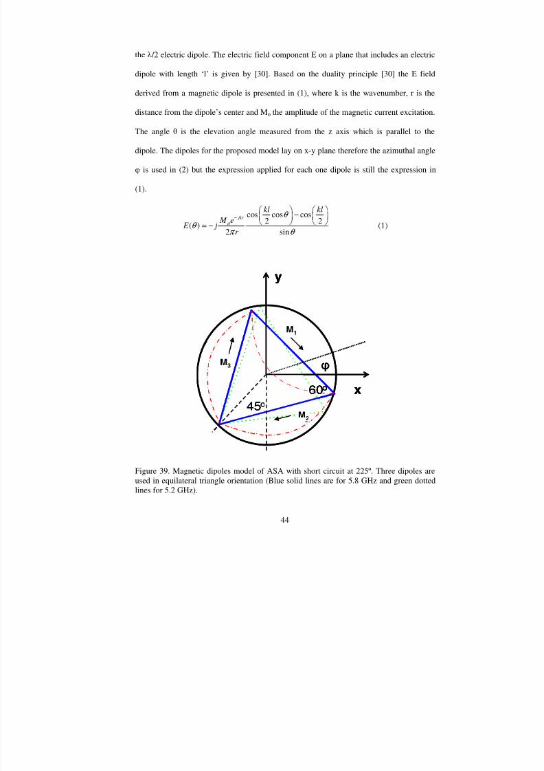
8/9/2019 Nikolaou Symeon 200512 Mast
http://slidepdf.com/reader/full/nikolaou-symeon-200512-mast 58/79
44
the λ /2 electric dipole. The electric field component E on a plane that includes an electric
dipole with length ‘l’ is given by [30]. Based on the duality principle [30] the E field
derived from a magnetic dipole is presented in (1), where k is the wavenumber, r is the
distance from the dipole’s center and Mo the amplitude of the magnetic current excitation.
The angle θ is the elevation angle measured from the z axis which is parallel to the
dipole. The dipoles for the proposed model lay on x-y plane therefore the azimuthal angle
φ is used in (2) but the expression applied for each one dipole is still the expression in
(1).
cos cos cos2 2
( )2 sin
jkr kl kl M e
E jr
ο
θ θ
π θ
− − −≃ (1)
60o x
y
45o
φΙο
Ιο
Ιο
60o x
y
45o
φΙο
Ιο
Ιο
M3
M1
M2
60o x
y
45o
φΙο
Ιο
Ιο
60o x
y
45o
φΙο
Ιο
Ιο
M3
M1
M2
Figure 39. Magnetic dipoles model of ASA with short circuit at 225º. Three dipoles are
used in equilateral triangle orientation (Blue solid lines are for 5.8 GHz and green dotted
lines for 5.2 GHz).

8/9/2019 Nikolaou Symeon 200512 Mast
http://slidepdf.com/reader/full/nikolaou-symeon-200512-mast 59/79
45
The superimposed electric field as a result of all three dipoles is given by (2) and is
plotted in Figure 40 in polar coordinates.
1 2 2
3 3
1 2
3
2( ) ( )
4 4 32
( )4 3
j j jkd
j jkd
E e E e e E
e e E
δ δ
δ
π π π φ φ
π π φ
−
− −
= + + + +
+ + −
(2)
0
-6.25
-12.5
-18.75
-250
30
60
90
120
150
180
210
240
270
300
330
Dipoles Model f=5.8 GHzNumerical Simulation f=5.8 GHz
Figure 40. Analytical expression plot of ASA with short circuit at 225º compared to the
numerical solution for the amplitude of E field.
The phase shift π /4 is used to take into consideration the respective dipoles’
orientation with respect to the reference axes. There is also a 2π /3 angle between two
consecutive dipoles which must be considered. In Figure 41 and Figure 42 the magnetic
current and phase distribution along the annular slot, are presented as derived from the

8/9/2019 Nikolaou Symeon 200512 Mast
http://slidepdf.com/reader/full/nikolaou-symeon-200512-mast 60/79
46
0 100 200 300 4000
0.2
0.4
0.6
0.8
1
1.2
1.4
An le de ree
N o r m a l i z e d C u r r e n t A m
p l i t u d e
f=5.8 GHz
f=5.2 GHz
f=6.4 GHz
M2 M1 M3
0 100 200 300 4000
0.2
0.4
0.6
0.8
1
1.2
1.4
An le de ree
N o r m a l i z e d C u r r e n t A m
p l i t u d e
f=5.8 GHz
f=5.2 GHz
f=6.4 GHz
M2 M1 M3
Figure 41. Magnetic Current amplitude distribution along the annular slot
0 100 200 300 400
-200
-150
-100
-50
0
50
100
150
200
An le de ree
C u r r e n t P h a s e
( d e g r e e )
f=5.8 GHzf=5.2 GHzf=6.4 GHz
-20o
+20o
-180o
0 100 200 300 400
-200
-150
-100
-50
0
50
100
150
200
An le de ree
C u r r e n t P h a s e
( d e g r e e )
f=5.8 GHzf=5.2 GHzf=6.4 GHz
-20o
+20o
-180o
Figure 42. Magnetic current phase distribution along the annular slot The 0 corresponds
to the short position. The singularity at 45o
is due the excitation source. The phases and
normalized amplitudes correspond to M2, M1 and M3 from left to the right.

8/9/2019 Nikolaou Symeon 200512 Mast
http://slidepdf.com/reader/full/nikolaou-symeon-200512-mast 61/79
47
electric field distribution presented in Figure 34. The magnetic current distribution
presented in Figure 41 matches the magnetic current distribution calculated and measured
for the shorted annular slot, presented in [5].
For expression (2) the amplitude and phase for each magnetic current excitation
must be estimated. The phases and amplitudes for the dipoles’ currents for f=5.8 GHz are
calculated from the solid lines in Figure 38 using the technique applied in [31]. The
phases, δ1, δ2 and δ3 are the phases of the current excitations and are calculated as the
mean values of the continuous phase distribution in the corresponding segment, as shown
in Figure 42. Therefore from Figure 42 the phases are estimated as δ2=-20
o
, δ1=-180
o
and
δ3=20o. The current amplitudes are normalized with respect to the strongest current M2,
which is the current on the segment where the excitation is applied. From Figure 41
M1=0.9M2 and M3=0.7M1 are deduced. The amplitudes descent in that order, because of
the traveling wave which is excited on the ring that attenuates as it propagates away from
from the excitation source. The path difference between E1 and E2, is d2=(λ /4)cos(60-φ)
while the path difference between E1 and E3 is d3=(λ /4)cos(60+φ) and can be easily
deduced geometrically from Figure 43. d2=(AA1). From orthogonal triangle AA1B
AA1= (AB)*cos(60-φ) where (AB)=λ /4. Similarly d1=(BB1) and from orthogonal
triangle CB1B (BB1)=(BC)*cos(60+φ) The normalized magnetic current excitations and
the phases used, apply for any design frequency for which the annular slot length is 3λ s /2.
The antenna prototype can be scaled for a different frequency without affecting the
validity of the model.

8/9/2019 Nikolaou Symeon 200512 Mast
http://slidepdf.com/reader/full/nikolaou-symeon-200512-mast 62/79
48
B
AC
B1
A1φ
φ
φ
B
AC
B1
A1φ
φ
φ
Figure 43. Three dipoles in equilateral triangle orientation
The analytical model predicts the null position and matches the numerical
solution with satisfactory precision as shown in Figure 40 for the central frequency, f=5.8
GHz. Measurements and the numerical solution show a shift in the null position as the
frequency changes, which is predicted by the dipole model. At a different frequency, the
slot circumference is no longer 3λ s /2 and a different field distribution occurs. As a result
the magnetic dipoles do not maintain their orientation with respect to the axes, but they
rotate slightly instead. For the lower frequency, the wavelength is about 10 % longer and
therefore the magnetic dipoles structure is rotated clockwise with the point at the short
fixed. The current distribution for f=5.2 GHz, for the dipole with M2 excitation requires a
longer segment along the ring (dotted line Figure 41) compared to the current 5.8 GHz.
The λ s /2 length at 5.2 GHz is about 10% longer than the one for 5.8 GHz so the dipoles

8/9/2019 Nikolaou Symeon 200512 Mast
http://slidepdf.com/reader/full/nikolaou-symeon-200512-mast 63/79
49
structure is rotated clockwise with the point at the short fixed (dotted straight lines in
Figure 39). The dipole with currents M1 and M3 behave accordingly. The dipole with M2
needs to be slightly shorter than λ s /2 since it terminates at the short position and it
overlaps with the feeding line. However it still remains close to λ s /2. Therefore the same
analytical expression (2) is used with the offset angle to be slightly greater than π /4. That
results in the rotation of the entire radiation pattern by the same offset angle clockwise as
can be seen in Figure 40. For the same reason, the use of a higher frequency at 6.4 GHz
results a counter-clockwise rotation of the null direction. The proposed model aims
primarily to give a qualitative explanation in the null shifting; therefore absolute
agreement with the numerical solution should not be expected. The microstrip feed line
and the matching circuits, which are only on one side of the ASA only, destroys the
symmetry. Therefore the null is stronger in the direction opposite to the feeding line as
can be seen in Figure 40 where the simulation results in all 4 quadrants are presented.
4.2 NULL POSITION RECONFIGURABLE DESIGN
For the null reconfigurable design, two stubs are used to match the antenna for the two
cases; when there is a short at ±45º away from the feeding line, and when no short exists
along the circumference. Consequently one small diode is used for the activation of the
matching stubs and two big diodes for the null control. When the small diode is not
biased and one of the two big diodes is biased, the antenna is matched at 5.8 GHz and
gives a null at 45o. When none of the big diodes are biased and the small diode is biased,
the antenna is matched at 5.8 GHz and a null appears in the direction opposite to the
feeding line. This second stub is placed at a distance D1=4.75 mm and has length
L1=2.97 mm. As a result, for a fixed frequency at 5.8 GHz a null in three different

8/9/2019 Nikolaou Symeon 200512 Mast
http://slidepdf.com/reader/full/nikolaou-symeon-200512-mast 64/79
50
directions (-45º, 0º, and +45º) can be created. The matching network design is presented
in Figure 44 and the dimensions are presented in Table III. The return loss measurements
for the hard-wired samples in comparison with the simulated results were presented in
Figure 38. The measurements for the samples with the diodes are presented in Figure 45.
Ls1 L1
D2D1 D3
L2
Ls2
x
y
Figure 44. ASA Null reconfigurable design matching network
TABLE III
Dimensions of circuit elements for null
reconfiguration at 5.8 GHz
Symbol Value in mm
D1 4.75
D2 7.27
D3 12.08
L1 2.97
L2 4.21
Ls1 6.50
Ls2 6.50

8/9/2019 Nikolaou Symeon 200512 Mast
http://slidepdf.com/reader/full/nikolaou-symeon-200512-mast 65/79
51
A small shift in the resonance frequency is consistently observed when a big
diode is biased along the slot. The capacitive load on the circumference results in a
downwards shift of the resonance frequency as discussed in [13]. For the null
reconfigurable design, the coexistence of two diodes on the slot with one of them forward
biased and the second one reverse biased results in a parasitic resonance close to 6.5
GHz, as seen in Figure 45. This is because of the additional capacitive load as a result of
the reverse biased diode. The parasitic resonance can be filtered with a cascaded
microstrip passband filter for the single frequency (5.8 GHz) null reconfigurable antenna.
For the extension to multiple frequencies, the parasitic will be taken care of with the
appropriate matching configuration. For the simulation, the reverse biased diode was
simulated as a perfect open and that is why the parasitic resonance does not appear in the
simulation. There is still a good resonance at the design frequency which is consistent for
all three directions of the null and is measured at 5.65 GHz which is less than 3% off the
design frequency.
4 5 6 7 8 9 10-40
-35
-30
-25
-20
-15
-10
-5
0
Frequency (GHz)
S 1 1 ( d B )
Sim with short at 225Right Big Diode BiasedLeft Big Diode BiasedSmall Diode Biased
Figure. 45. Diodes effect in return loss measurement for the null reconfigurable design.
The design frequency was 5.8 GHz.

8/9/2019 Nikolaou Symeon 200512 Mast
http://slidepdf.com/reader/full/nikolaou-symeon-200512-mast 66/79
52
4.3 RADIATION PATTERN MEASUREMENTS
A far field antenna test range was used to characterize the ASA. In the test range,
the ASA was the receiving antenna that rotated through the φ plane while a 5.4-8.2 GHz,
15 dB standard gain horn was used as the fixed, transmitting antenna; the two antennas
were separated by 1 m. The transmitted RF signal was AM modulated by a 20 MHz
signal that was detected by a diode detector and measured by a lock-in amplifier. Control
of the rotary stage, lock-in amplifier, and data recording was automated. To bias the
diodes, wires were soldered to the center of the ASA and the radial stubs of the matching
circuit. In addition, a bias tee was used to ground the microstrip line and to isolate the
applied bias from the diode detector. Because the ASA radiates backward as well as
forward, the coaxial launcher, bias tee, and detector were sandwiched between 1 cm thick
pieces of absorbing material. Before characterizing the ASA, a variable attenuator was
used to vary the input power in order to calibrate the diode detector and determine the
radiated power that results in maximum detector sensitivity. During test, it was observed
that the substrate corners had to be rounded (Figure 46) to minimize reflections and
diffractions at the corners that caused ripples in the radiation pattern. A measurement
taken before the corners were rounded is presented in Figure 47. The ripple in the 135o
direction because of the diffraction on the board corner is obvious.
The effect of both the small and big diodes on the radiation patterns was
investigated and is presented in the current section, and the radiation patterns are
compared to the simulation results (ideal elements) and to the hard-wired design
measurements presented earlier. In Figure 48, the measured radiation patterns for the Eφ

8/9/2019 Nikolaou Symeon 200512 Mast
http://slidepdf.com/reader/full/nikolaou-symeon-200512-mast 67/79
53
component of the electric field, which is the component parallel to the antenna substrate,
for all three frequencies and
Figure 46. Photograph of the tested ASA with the rounded corners. The dc probes for the
diodes bias can be seen.
Figure 47. Eφ radiation pattern at 5.8 GHz with the short along the slot circumference

8/9/2019 Nikolaou Symeon 200512 Mast
http://slidepdf.com/reader/full/nikolaou-symeon-200512-mast 68/79
54
a hard-wired short at 225º are shown. In addition, the measured radiation pattern at 5.2
GHz for a regular slot without any short along the slot is shown. The results in Fig. 44
have similar behavior to the simulated results presented in Figure 37 in section 3.1. The
shift in the null direction with respect to the frequency that was explained in a previous
section is hereby verified experimentally.
Figure 48. Measured radiation patterns for the design frequencies when a hard- wiredshort is placed at 225o
Figure 49 and Figure 50 present the measured radiation patterns for frequencies of
5.2 GHz and 6.4 GHz respectively with diodes used to short the slot. They were in very
good agreement with the simulation and the hard-wired measurements. This proves that
the PIN diode is a suitable switch for this application. The effectiveness of the small
diodes has been verified in designs other than antennas, like filters [32] and it only has to
do with the matching network. The parasitic capacitance and resistive load of the big
diodes that differentiate them from the ideal short circuit, on the other hand, have been

8/9/2019 Nikolaou Symeon 200512 Mast
http://slidepdf.com/reader/full/nikolaou-symeon-200512-mast 69/79

8/9/2019 Nikolaou Symeon 200512 Mast
http://slidepdf.com/reader/full/nikolaou-symeon-200512-mast 70/79
56
The short was placed in symmetrical positions with respect to the feeding line
direction in order to show that the results are not dependent on the side of the short and
are not affected from the non symmetric matching stubs. The behavior of the antenna is
equivalent for both sides of the short.
In the plots presented in Figures 49 and 50, the measurements were taken for
different samples in order to compare and evaluate the effect of small and big diodes
independently. For the null reconfigurable design (Figures 51 and 52) all measurements
were taken for the same sample on which three diodes are used and biased individually to
steer the null in the three directions and maintain a constant resonant frequency. In order
to get the nulls in the side directions, the corresponding big diode is biased. In order to
get the null in the feeding line direction, the small diode on the matching stub L1 in
Figure 44 is biased in order to maintain the resonance frequency constant at 5.65 GHz
while none of the big diodes is biased. In Figure 51 and Figure 52 where the simulated
and measured results are presented, respectively, it is obvious that the steering of the null
is achieved with high precision. The slot dimensions are optimized for the frequency of
5.8 GHz and for that frequency the null is exactly at 45o
off the feed line direction. The
measured patterns are for f=5.65 GHz which is very close to the design frequency and as
a result the null directions verify the simulation with high accuracy. In the 90o
direction
the simulated field is stronger than the measurement but overall good agreement is
demonstrated.

8/9/2019 Nikolaou Symeon 200512 Mast
http://slidepdf.com/reader/full/nikolaou-symeon-200512-mast 71/79

8/9/2019 Nikolaou Symeon 200512 Mast
http://slidepdf.com/reader/full/nikolaou-symeon-200512-mast 72/79
58
4.4 SUMMARY
The null position reconfigurable design has been presented in this chapter. The
null position has been steered using switches implemented with pin diodes along the
aperture circumference. This behavior has been analyzed in detail with a novel, simple
but accurate model using three magnetic dipoles in equilateral triangle orientation to
substitute the magnetic current within the slot. The model has justified adequately the
reorientation of the null when a short is used to load the slot, and the small shift in the
mull position when the slot circumference is perturbed from the optimized 3λ s /2 length.
The proposed antenna was fabricated and tested. The use of diodes and their
performance compared to hard-wire shorts has been demonstrated. The radiation pattern
measurements were in good agreement with the simulated results. The measurements
procedure has been described and experimental techniques have been suggested to
overcome measurements inconsistency.
The radiation pattern analysis and the experimental verification conclude the
study on the proposed reconfigurable in frequency and radiation pattern Annular Slot
Antenna.

8/9/2019 Nikolaou Symeon 200512 Mast
http://slidepdf.com/reader/full/nikolaou-symeon-200512-mast 73/79
59
CHAPTER 5
CONCLUSION AND POTENTIAL APPLICATIONS
The goal of this thesis has been to develop and optimize a single antenna that
would demonstrate a reconfigurable frequency of operation and a reconfigurable
radiation pattern. This antenna has been designed to operate in a very popular frequency
range where a great number of wireless communication applications exist. From this
analysis, it has been concluded that a successful, low cost reconfigurable antenna design
has been introduced to the wireless and radio frequency design community.
A new design for both pattern and frequency reconfigurable annular slot antenna
was presented. Matching stubs were used to match the antenna to three different
frequencies, 5.2 GHz and 6.4 GHz in addition to the initial central frequency at 5.8 GHz.
PIN diodes were used to connect or disconnect the stubs creating a reconfigurable
matching network. The radiation pattern control was achieved by activating/deactivating
shorts on the slot. As a result the null was redirected to a different direction. As a
benchmarking approach, the shorts were implemented by use of pin diodes. When each
diode was forward biased, it was equivalent to a short, and when it was reverse biased, it
behaved as a capacitive load. In the latter case, when no diodes were forward biased, the
slot antenna behaved like the unloaded slot antenna and the null appears in the feeding
line direction. The results for this antenna were presented at three separate frequencies.
Any other frequency can be matched using the same technique as long as the
radiation efficiency for that frequency is satisfactory. The same applies with the position
of the shorts. The possible directions are not limited to the ones used in this study but in

8/9/2019 Nikolaou Symeon 200512 Mast
http://slidepdf.com/reader/full/nikolaou-symeon-200512-mast 74/79
60
that case also, the matching stubs need to be redesigned and optimized for the preferred
short direction, since the short direction affects the equivalent load at the end of the
transmission line. The measured results were compared to the simulations and were
found to be in very good agreement. The proposed antenna is compact and easy to
integrate with other microwave components.
There is a great number of applications for this kind of reconfigurable antenna.
This antenna is the first step towards more mature compact reconfigurable slot antennas
both in frequency and radiation pattern using pin diodes or RF MEMS switches. The
ASA can be used as a mobile device antenna, although the fact that direction of the
interferer is completely random would require a more sophisticated and complicated
antenna structure. The antenna can find application in cases where interference in the x-y
plane needs to be minimized. In practical scenarios, this can be useful if combined with a
mechanical motion of the antenna where the plane of the antenna can also be moved.
Another application could be the interference minimization in an antenna array
environment. The proposed antenna can be used as planar array element. In a
reconfigurable array, where different combination of elements can be active at a time, the
creation of nulls in pre-selected desired positions give a design parameter to control the
mutual coupling between neighboring elements. At the same time, the directivity in the
broadside direction remains equally high.

8/9/2019 Nikolaou Symeon 200512 Mast
http://slidepdf.com/reader/full/nikolaou-symeon-200512-mast 75/79
61
APPENDIX A
LIST OF PUBLICATIONS
[1] S.Nikolaou, G.E.Ponchak, J.Papapolymerou and M.M.Tentzeris, "Shorted Annular
Slot Antenna (ASA) Matched at Three Different Frequencies", IEEE-APS
Symposium, Washington, DC, July 2005
[2] S.Nikolaou, G.E.Ponchak, J.Papapolymerou and M.M.Tentzeris, “Design and
Development of an Annular Slot Antenna (ASA) with a Reconfigurable Radiation
Pattern” Accepted for presentation in APMC 2005 Asia-Pacific Microwave
Conference Suzhou, China, December 2005.
[3] S. Nikolaou, R.Bairavasubramanian, C. Lugo Jr.,I. Carrasquillo, D.C. Thompson,G.E. Ponchak, J. Papapolymerou, M. M. Tentzeris, “Pattern and Frequency
Reconfigurable Annular Slot Antenna using PIN Diodes.” Accepted for publication
in IEEE Transactions on Antennas and Propagation, February, 2006

8/9/2019 Nikolaou Symeon 200512 Mast
http://slidepdf.com/reader/full/nikolaou-symeon-200512-mast 76/79
62
REFERENCES
[1] D. M. Pozar, “Reciprocity method of analysis for printed slot and slot–coupled
microstrip antennas”, IEEE Transactions on Antennas and Propagation, Vol. AP-34,
pp. 1439 – 1446, 1986
[2] A. Axelrod, M. Kilsiuk, and J. Maoz, “Broadband microstrip-fed slot radiator”,
Microwave J., pp.81-94, 1989.
[3] Garg, P. Bhartia, I. Bahl, A. Ittipibbon, “ Micostrip antenna design handbook”,
Artech House, pp. 441-491, 2001
[4] H. Morishita, K. Hirasawa, and K. Fujimoto, “ Analysis of a cavity-backed annular
slot antenna with one point shorted”, IEEE Transactions on Antennas and
Propagation, vol. 39, no.10, pp. 1472 – 1478, October 1991.
[5] J.T. Bernhard,R. Wang, R. Clark, and P. Mayes, “Stacked reconfigurable antenna
elements for space-based radar applications”, IEEE Antennas and Propagation
Society International Symposium, Vol. 1, pp. 158 – 161, July 2001.
[6] K. Tomiyasu, “Conceptual reconfigurable antenna for 35 GHz high-resolution
spaceborne synthetic aperture radar”, IEEE Transactions on Aerospace and
Electronic Systems, Vol. 39, Issue: 3, pp. 1069 – 1074, July 2003.
[7] J.T. Aberle, Sung-Hoon Oh, D.T. Auckland, and S.D. Rogers, “Reconfigurable
antennas for wireless devices” IEEE Antennas and Propagation Magazine, Vol.
45, Issue: 6 , pp. 148 – 154, December 2003.
[8] G.H. Huff, J. Feng, Shenghui Zhang, G. Cung, and J.T. Bernhard “Directional
reconfigurable antennas on laptop computers: Simulation, measurement and
evaluation of candidate integration positions”, IEEE Transactions on Antennas and
Propagation, Vol. 52, Issue:12, pp. 3220 – 3227, December 2004.
[9] W.H. Weedon, W.J. Payne, and G.M. Rebeiz, “MEMS-switched reconfigurable
antennas” IEEE Antennas and Propagation Society International Symposium, Vol.
3, pp. 654 – 657, July 2001.

8/9/2019 Nikolaou Symeon 200512 Mast
http://slidepdf.com/reader/full/nikolaou-symeon-200512-mast 77/79
63
[10] C. E. Tong, and R. Blundel, “An annular slot antenna on a dielectric half-space”,
IEEE Transactions on Antennas and Propagation, Vol. 2, no.7, pp. 967 – 974, July
1994.
[11] S. Kanamaluru, Ming-Yi L, and Kai Chang, “Narrowband filter and annular slot
antenna for PCS applications”, IEEE MTT-S International Microwave Symposium
Digest, Vol. 2 , pp. 987 – 990, June 1996.
[12] Cheng-Shong Hong, “Small annular slot antenna with capacitor loading” Electronics
Letters , vol.36 , no.2, pp. 110 – 111, January 2000.
[13] K. Prasad, and L. Shafai, “‘Higher order mode excitation in circular loop and
annular slot antennas”, IEEE Antennas and Propagation Society International
Symposium, Vol. 25, pp. 824 – 827, Jun 1987.
[14] P. Mastin, B. Rawat and M., Williamson,”Design of a microstrip annular slot
antenna for mobile communications” IEEE Antennas and Propagation Society
International Symposium Digest. Held in Conjuction with: URSI Radio Science
Meeting and Nuclear EMP Meeting, Vol. 1, pp. 507 – 510, July 1992.
[15] E. Irzinski, “The input admittance of a TEM excited annular slot antenna”, IEEE
Transactions on Antennas and Propagation, Vol. 23, Issue: 6, pp. 829 –
834, November 1975.
[16] N. Nikolic, J.S. Kot, and T.S. Bird, “Theoretical and experimental study of a cavity-
backed annular-slot antenna”, IEE Proceedings on Microwaves, Antennas and
Propagation, Vol. 144, Issue: 5 , pp. 337 – 340, October 1997.
[17] Ming-Hau Yeh, Powen Hsu, and Jean-Fu Kiang, “Analysis of a CPW-fed slot ring
antenna”, Asia-Pacific Microwave Conference, Vol. 3, pp. 1267 - 1270 , December
2001.
[18] P. Minard, and A. Louzir, “A new wide frequency band feeding technique of annular
slot antenna”, IEEE Antennas and Propagation Society International Symposium,
Vol. 1, pp. 406 – 409, June 2002.
[19] H. Tehrani and Kai Chang, “A multi-frequency microstrip-fed annular slot antenna”,
IEEE Antennas and Propagation Society International Symposium, Vol. 2, pp. 632 –
635, July 2000.

8/9/2019 Nikolaou Symeon 200512 Mast
http://slidepdf.com/reader/full/nikolaou-symeon-200512-mast 78/79
64
[20] F. Le Bolter, and A. Louzir, “Multi-band annular slot antenna for WLAN
applications”, IEEE Antennas and Propagation Society Conference, Vol. 2, pp. 529
– 532, April 2001.
[21] Quan Li, Zhongxiang Shen and Xiaoyong Shan, “A new microstrip-fed cavity-
backed annular slot antenna”, IEEE Antennas and Propagation Society International
Symposium, Vol. 3, pp.68, June 2002.
[22] Young Hoon Suh and Ikmo Park, “A broadband eccentric annular slot antenna”
IEEE Antennas and Propagation Society International Symposium, Vol. 1, pp. 94 –
97, July 2001.
[21] N. Behdad and K. Sarabandi, “A wideband bi-semicircular slot antenna”, IEEE
Antennas and Propagation Society Symposium, Vol.2, pp. 1903 – 1906, June 2004
[22] D.Peroulis, K. Sarabandi, L.P.B. Katehi, “Design of reconfigurable slot antennas”,
IEEE Transactions on Antennas and Propagation, Vol. 53, Issue 2, pp. 645 – 654,
February 2005
[23] P. R. Urwin-Wright, G.S. Hilton, I. J. Craddock, and P. N. Fletcher, “An
electrically-small annular slot operating in the 'DC' mode”, Twelfth International
Conference on Antennas and Propagation, Vol. 2, pp. 686 – 689, April 2003
[23] RongLin Li, G.DeJean, M.M. Tentzeris, and J. Laskar, “Development and analysisof a folded shorted-patch antenna with reduced size”, IEEE Transactions on
Antennas and Propagation, Vol. 52, Issue: 2, pp. 555 – 562, February 2004.
[24] P. Hallbjorner, “Electrically small unbalanced four-arm wire antenna” IEEE
Transactions on Antennas and Propagation, Vol. 52, Issue: 6, pp. 1424 – 1428, June
2004.
[25] Ansoft HFSS
[26] C. A. Balanis, “Antenna Theory Analysis and Design”, John Wiley & sons, Second
Edition, pp. 152 –157.
[27] R. L. Li, V. F. Fusco and R. Cahil, “Pattern shaping using a reactively loaded wire
loop antenna”, IEE Proceedings on Microwaves, Antennas and Propagation, Vol.
148, Issue: 3, pp. 203 – 208, June 2004

8/9/2019 Nikolaou Symeon 200512 Mast
http://slidepdf.com/reader/full/nikolaou-symeon-200512-mast 79/79
[28] C.Lugo and J. Papapolymerou, “Electronic switchable bandpass filter using PIN
diodes for wireless low cost system-on-a-package applications.” IEE Proceedings on
Microwaves, Antennas and Propagation, Vol. 151, Issue: 6, pp. 497 – 502,
December 2004.