Microwave purification of large-area horizontally aligned ...
40
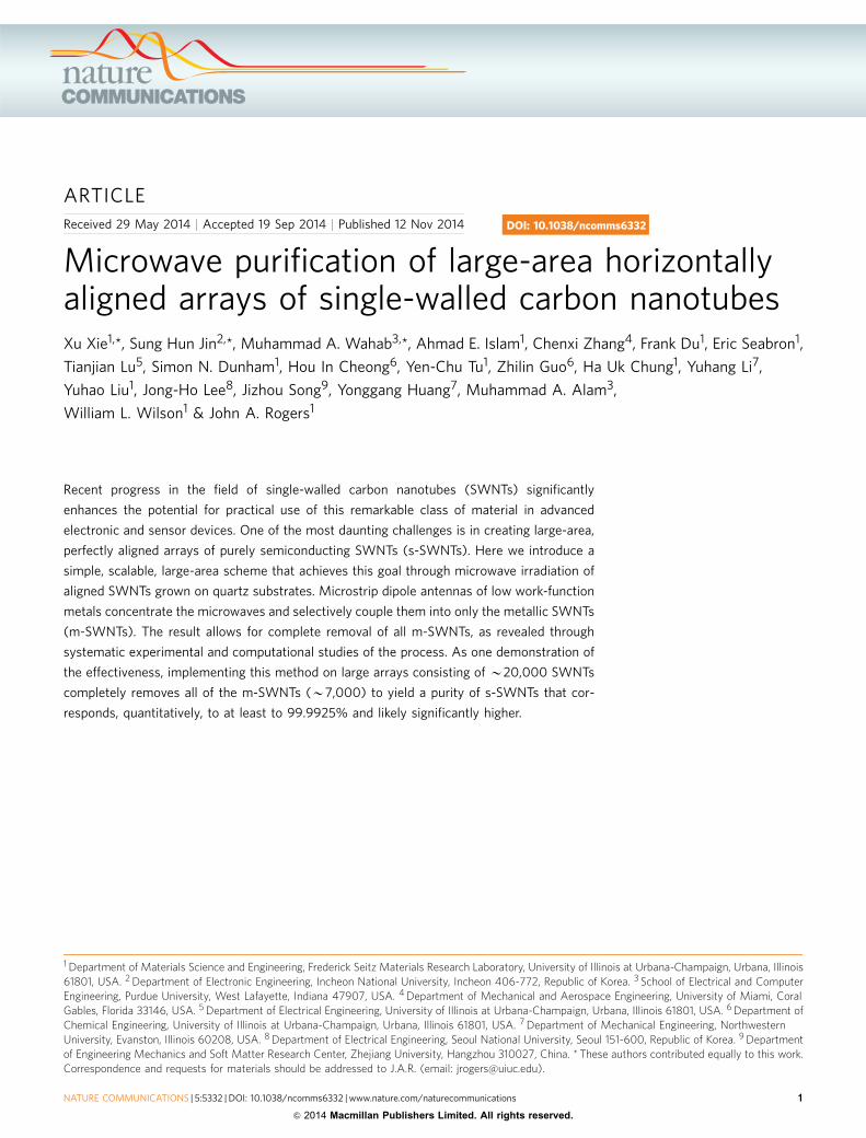
ARTICLE Received 29 May 2014 | Accepted 19 Sep 2014 | Published 12 Nov 2014 Microwave purification of large-area horizontally aligned arrays of single-walled carbon nanotubes Xu Xie 1, *, Sung Hun Jin 2, *, Muhammad A. Wahab 3, *, Ahmad E. Islam 1 , Chenxi Zhang 4 , Frank Du 1 , Eric Seabron 1 , Tianjian Lu 5 , Simon N. Dunham 1 , Hou In Cheong 6 , Yen-Chu Tu 1 , Zhilin Guo 6 , Ha Uk Chung 1 , Yuhang Li 7 , Yuhao Liu 1 , Jong-Ho Lee 8 , Jizhou Song 9 , Yonggang Huang 7 , Muhammad A. Alam 3 , William L. Wilson 1 & John A. Rogers 1 Recent progress in the field of single-walled carbon nanotubes (SWNTs) significantly enhances the potential for practical use of this remarkable class of material in advanced electronic and sensor devices. One of the most daunting challenges is in creating large-area, perfectly aligned arrays of purely semiconducting SWNTs (s-SWNTs). Here we introduce a simple, scalable, large-area scheme that achieves this goal through microwave irradiation of aligned SWNTs grown on quartz substrates. Microstrip dipole antennas of low work-function metals concentrate the microwaves and selectively couple them into only the metallic SWNTs (m-SWNTs). The result allows for complete removal of all m-SWNTs, as revealed through systematic experimental and computational studies of the process. As one demonstration of the effectiveness, implementing this method on large arrays consisting of B20,000 SWNTs completely removes all of the m-SWNTs (B7,000) to yield a purity of s-SWNTs that cor- responds, quantitatively, to at least to 99.9925% and likely significantly higher. DOI: 10.1038/ncomms6332 1 Department of Materials Science and Engineering, Frederick Seitz Materials Research Laboratory, University of Illinois at Urbana-Champaign, Urbana, Illinois 61801, USA. 2 Department of Electronic Engineering, Incheon National University, Incheon 406-772, Republic of Korea. 3 School of Electrical and Computer Engineering, Purdue University, West Lafayette, Indiana 47907, USA. 4 Department of Mechanical and Aerospace Engineering, University of Miami, Coral Gables, Florida 33146, USA. 5 Department of Electrical Engineering, University of Illinois at Urbana-Champaign, Urbana, Illinois 61801, USA. 6 Department of Chemical Engineering, University of Illinois at Urbana-Champaign, Urbana, Illinois 61801, USA. 7 Department of Mechanical Engineering, Northwestern University, Evanston, Illinois 60208, USA. 8 Department of Electrical Engineering, Seoul National University, Seoul 151-600, Republic of Korea. 9 Department of Engineering Mechanics and Soft Matter Research Center, Zhejiang University, Hangzhou 310027, China. *These authors contributed equally to this work. Correspondence and requests for materials should be addressed to J.A.R. (email: [email protected]). NATURE COMMUNICATIONS | 5:5332 | DOI: 10.1038/ncomms6332 | www.nature.com/naturecommunications 1 & 2014 Macmillan Publishers Limited. All rights reserved.
Transcript of Microwave purification of large-area horizontally aligned ...
ARTICLE
Received 29 May 2014 | Accepted 19 Sep 2014 | Published 12 Nov 2014
Microwave purification of large-area horizontallyaligned arrays of single-walled carbon nanotubesXu Xie1,*, Sung Hun Jin2,*, Muhammad A. Wahab3,*, Ahmad E. Islam1, Chenxi Zhang4, Frank Du1, Eric Seabron1,
Tianjian Lu5, Simon N. Dunham1, Hou In Cheong6, Yen-Chu Tu1, Zhilin Guo6, Ha Uk Chung1, Yuhang Li7,
Yuhao Liu1, Jong-Ho Lee8, Jizhou Song9, Yonggang Huang7, Muhammad A. Alam3,
William L. Wilson1 & John A. Rogers1
Recent progress in the field of single-walled carbon nanotubes (SWNTs) significantly
enhances the potential for practical use of this remarkable class of material in advanced
electronic and sensor devices. One of the most daunting challenges is in creating large-area,
perfectly aligned arrays of purely semiconducting SWNTs (s-SWNTs). Here we introduce a
simple, scalable, large-area scheme that achieves this goal through microwave irradiation of
aligned SWNTs grown on quartz substrates. Microstrip dipole antennas of low work-function
metals concentrate the microwaves and selectively couple them into only the metallic SWNTs
(m-SWNTs). The result allows for complete removal of all m-SWNTs, as revealed through
systematic experimental and computational studies of the process. As one demonstration of
the effectiveness, implementing this method on large arrays consisting of B20,000 SWNTs
completely removes all of the m-SWNTs (B7,000) to yield a purity of s-SWNTs that cor-
responds, quantitatively, to at least to 99.9925% and likely significantly higher.
DOI: 10.1038/ncomms6332
1 Department of Materials Science and Engineering, Frederick Seitz Materials Research Laboratory, University of Illinois at Urbana-Champaign, Urbana, Illinois61801, USA. 2 Department of Electronic Engineering, Incheon National University, Incheon 406-772, Republic of Korea. 3 School of Electrical and ComputerEngineering, Purdue University, West Lafayette, Indiana 47907, USA. 4 Department of Mechanical and Aerospace Engineering, University of Miami, CoralGables, Florida 33146, USA. 5 Department of Electrical Engineering, University of Illinois at Urbana-Champaign, Urbana, Illinois 61801, USA. 6 Department ofChemical Engineering, University of Illinois at Urbana-Champaign, Urbana, Illinois 61801, USA. 7 Department of Mechanical Engineering, NorthwesternUniversity, Evanston, Illinois 60208, USA. 8 Department of Electrical Engineering, Seoul National University, Seoul 151-600, Republic of Korea. 9 Departmentof Engineering Mechanics and Soft Matter Research Center, Zhejiang University, Hangzhou 310027, China. * These authors contributed equally to this work.Correspondence and requests for materials should be addressed to J.A.R. (email: [email protected]).
NATURE COMMUNICATIONS | 5:5332 | DOI: 10.1038/ncomms6332 | www.nature.com/naturecommunications 1
& 2014 Macmillan Publishers Limited. All rights reserved.
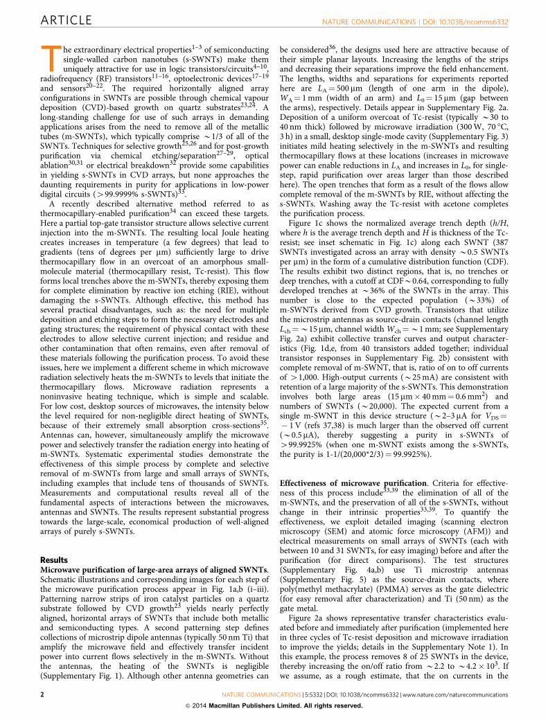
The extraordinary electrical properties1–3 of semiconductingsingle-walled carbon nanotubes (s-SWNTs) make themuniquely attractive for use in logic transistors/circuits4–10,
radiofrequency (RF) transistors11–16, optoelectronic devices17–19
and sensors20–22. The required horizontally aligned arrayconfigurations in SWNTs are possible through chemical vapourdeposition (CVD)-based growth on quartz substrates23,24. Along-standing challenge for use of such arrays in demandingapplications arises from the need to remove all of the metallictubes (m-SWNTs), which typically comprise B1/3 of all of theSWNTs. Techniques for selective growth25,26 and for post-growthpurification via chemical etching/separation27–29, opticalablation30,31 or electrical breakdown32 provide some capabilitiesin yielding s-SWNTs in CVD arrays, but none approaches thedaunting requirements in purity for applications in low-powerdigital circuits (499.9999% s-SWNTs)33.
A recently described alternative method referred to asthermocapillary-enabled purification34 can exceed these targets.Here a partial top-gate transistor structure allows selective currentinjection into the m-SWNTs. The resulting local Joule heatingcreates increases in temperature (a few degrees) that lead togradients (tens of degrees per mm) sufficiently large to drivethermocapillary flow in an overcoat of an amorphous small-molecule material (thermocapillary resist, Tc-resist). This flowforms local trenches above the m-SWNTs, thereby exposing themfor complete elimination by reactive ion etching (RIE), withoutdamaging the s-SWNTs. Although effective, this method hasseveral practical disadvantages, such as: the need for multipledeposition and etching steps to form the necessary electrodes andgating structures; the requirement of physical contact with theseelectrodes to allow selective current injection; and residue andother contamination that often remains, even after removal ofthese materials following the purification process. To avoid theseissues, here we implement a different scheme in which microwaveradiation selectively heats the m-SWNTs to levels that initiate thethermocapillary flows. Microwave radiation represents anoninvasive heating technique, which is simple and scalable.For low cost, desktop sources of microwaves, the intensity belowthe level required for non-negligible direct heating of SWNTs,because of their extremely small absorption cross-sections35.Antennas can, however, simultaneously amplify the microwavepower and selectively transfer the radiation energy into heating ofm-SWNTs. Systematic experimental studies demonstrate theeffectiveness of this simple process by complete and selectiveremoval of m-SWNTs from large and small arrays of SWNTs,including examples that include tens of thousands of SWNTs.Measurements and computational results reveal all of thefundamental aspects of interactions between the microwaves,antennas and SWNTs. The results represent substantial progresstowards the large-scale, economical production of well-alignedarrays of purely s-SWNTs.
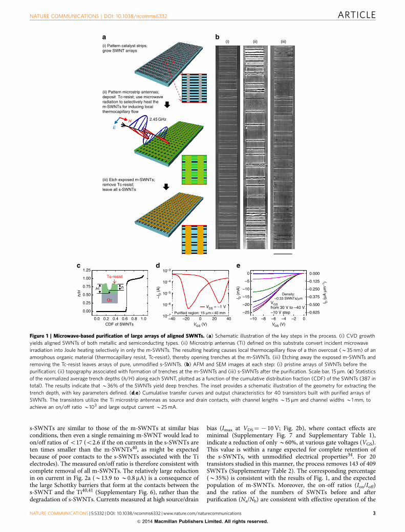
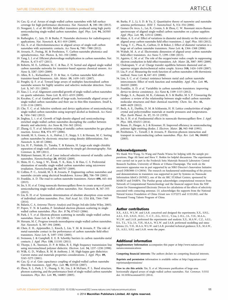
ResultsMicrowave purification of large-area arrays of aligned SWNTs.Schematic illustrations and corresponding images for each step ofthe microwave purification process appear in Fig. 1a,b (i–iii).Patterning narrow strips of iron catalyst particles on a quartzsubstrate followed by CVD growth23 yields nearly perfectlyaligned, horizontal arrays of SWNTs that include both metallicand semiconducting types. A second patterning step definescollections of microstrip dipole antennas (typically 50 nm Ti) thatamplify the microwave field and effectively transfer incidentpower into current flows selectively in the m-SWNTs. Withoutthe antennas, the heating of the SWNTs is negligible(Supplementary Fig. 1). Although other antenna geometries can
be considered36, the designs used here are attractive because oftheir simple planar layouts. Increasing the lengths of the stripsand decreasing their separations improve the field enhancement.The lengths, widths and separations for experiments reportedhere are LA¼ 500 mm (length of one arm in the dipole),WA¼ 1 mm (width of an arm) and L0¼ 15 mm (gap betweenthe arms), respectively. Details appear in Supplementary Fig. 2a.Deposition of a uniform overcoat of Tc-resist (typically B30 to40 nm thick) followed by microwave irradiation (300 W, 70 C,3 h) in a small, desktop single-mode cavity (Supplementary Fig. 3)initiates mild heating selectively in the m-SWNTs and resultingthermocapillary flows at these locations (increases in microwavepower can enable reductions in LA and increases in L0, for single-step, rapid purification over areas larger than those describedhere). The open trenches that form as a result of the flows allowcomplete removal of the m-SWNTs by RIE, without affecting thes-SWNTs. Washing away the Tc-resist with acetone completesthe purification process.
Figure 1c shows the normalized average trench depth (h/H,where h is the average trench depth and H is thickness of the Tc-resist; see inset schematic in Fig. 1c) along each SWNT (387SWNTs investigated across an array with density B0.5 SWNTsper mm) in the form of a cumulative distribution function (CDF).The results exhibit two distinct regions, that is, no trenches ordeep trenches, with a cutoff at CDFB0.64, corresponding to fullydeveloped trenches at B36% of the SWNTs in the array. Thisnumber is close to the expected population (B33%) ofm-SWNTs derived from CVD growth. Transistors that utilizethe microstrip antennas as source-drain contacts (channel lengthLch¼B15mm, channel width Wch¼B1 mm; see SupplementaryFig. 2a) exhibit collective transfer curves and output character-istics (Fig. 1d,e, from 40 transistors added together; individualtransistor responses in Supplementary Fig. 2b) consistent withcomplete removal of m-SWNT, that is, ratio of on to off currentsof 41,000. High-output currents (B25 mA) are consistent withretention of a large majority of the s-SWNTs. This demonstrationinvolves both large areas (15 mm 40 mm¼ 0.6 mm2) andnumbers of SWNTs (B20,000). The expected current from asingle m-SWNT in this device structure (B2–3mA for VDS¼ 1 V (refs 37,38) is much larger than the observed off current(B0.5 mA), thereby suggesting a purity in s-SWNTs of499.9925% (when one m-SWNT exists among the s-SWNTs,the purity is 1-1/(20,000*2/3)¼ 99.9925%).
Effectiveness of microwave purification. Criteria for effective-ness of this process include33,39 the elimination of all of them-SWNTs, and the preservation of all of the s-SWNTs, withoutchange in their intrinsic properties33,39. To quantify theeffectiveness, we exploit detailed imaging (scanning electronmicroscopy (SEM) and atomic force microscopy (AFM)) andelectrical measurements on small arrays of SWNTs (each withbetween 10 and 31 SWNTs, for easy imaging) before and after thepurification (for direct comparisons). The test structures(Supplementary Fig. 4a,b) use Ti microstrip antennas(Supplementary Fig. 5) as the source-drain contacts, wherepoly(methyl methacrylate) (PMMA) serves as the gate dielectric(for easy removal after characterization) and Ti (50 nm) as thegate metal.
Figure 2a shows representative transfer characteristics evalu-ated before and immediately after purification (implemented herein three cycles of Tc-resist deposition and microwave irradiationto improve the yields; details in the Supplementary Note 1). Inthis example, the process removes 8 of 25 SWNTs in the device,thereby increasing the on/off ratio from B2.2 to B4.2 103. Ifwe assume, as a rough estimate, that the on currents in the
ARTICLE NATURE COMMUNICATIONS | DOI: 10.1038/ncomms6332
2 NATURE COMMUNICATIONS | 5:5332 | DOI: 10.1038/ncomms6332 | www.nature.com/naturecommunications
& 2014 Macmillan Publishers Limited. All rights reserved.
s-SWNTs are similar to those of the m-SWNTs at similar biasconditions, then even a single remaining m-SWNT would lead toon/off ratios of o17 (o2.6 if the on currents in the s-SWNTs areten times smaller than the m-SWNTs40, as might be expectedbecause of poor contacts to the s-SWNTs associated with the Tielectrodes). The measured on/off ratio is therefore consistent withcomplete removal of all m-SWNTs. The relatively large reductionin on current in Fig. 2a (B13.9 to B0.8 mA) is a consequence ofthe large Schottky barriers that form at the contacts between thes-SWNT and the Ti40,41 (Supplementary Fig. 6), rather than thedegradation of s-SWNTs. Currents measured at high source/drain
bias (Imax at VDS¼ 10 V; Fig. 2b), where contact effects areminimal (Supplementary Fig. 7 and Supplementary Table 1),indicate a reduction of only B60%, at various gate voltages (VGS).This value is within a range expected for complete retention ofthe s-SWNTs, with unmodified electrical properties34. For 20transistors studied in this manner, the process removes 143 of 409SWNTs (Supplementary Table 2). The corresponding percentage(B35%) is consistent with the results of Fig. 1, and the expectedpopulation of m-SWNTs. Moreover, the on-off ratios (Ion/Ioff)and the ratios of the numbers of SWNTs before and afterpurification (Na/Nb) are consistent with effective operation of the
(i) (ii) (iii)
2.45 GHz
(i) Pattern catalyst strips;grow SWNT arrays
(ii) Pattern microstrip antennas; deposit Tc-resist; use microwaveradiation to selectively heat the m-SWNTs for inducing localthermocapillary flow
(iii) Etch exposed m-SWNTs;remove Tc-resist;leave all s-SWNTs
H
E
10–31.25
1.00 Tc-resist
Qz
0.75
0.50
H h
h/H
–lD (
A)
l D (
mA
)
l D (
μA μ
m–1
)
0.25
0.00
0.0 0.2 0.4 0.6 0.8CDF of SWNTs
1.0 –40 –20VGS (V)
Purified region: 15 μm × 40 mm
VDS = –1 V
0 20 40 –10
–25
–20
–15
–10Density:
~0.33 SWNTs/μmVGSfrom 30 V to –40 V.–10 V step
–5
0
–8 –6VDS (V)
–4 –2 0
–0.625
–0.500
–0.375
–0.250
–0.125
0.000
10–4
10–5
10–6
10–7
Figure 1 | Microwave-based purification of large arrays of aligned SWNTs. (a) Schematic illustration of the key steps in the process. (i) CVD growth
yields aligned SWNTs of both metallic and semiconducting types. (ii) Microstrip antennas (Ti) defined on this substrate convert incident microwave
irradiation into Joule heating selectively in only the m-SWNTs. The resulting heating causes local thermocapillary flow of a thin overcoat (B35 nm) of an
amorphous organic material (thermocapillary resist, Tc-resist), thereby opening trenches at the m-SWNTs. (iii) Etching away the exposed m-SWNTs and
removing the Tc-resist leaves arrays of pure, unmodified s-SWNTs. (b) AFM and SEM images at each step: (i) pristine arrays of SWNTs before the
purification; (ii) topography associated with formation of trenches at the m-SWNTs and (iii) s-SWNTs after the purification. Scale bar, 15mm. (c) Statistics
of the normalized average trench depths (h/H) along each SWNT, plotted as a function of the cumulative distribution fraction (CDF) of the SWNTs (387 in
total). The results indicate that B36% of the SWNTs yield deep trenches. The inset provides a schematic illustration of the geometry for extracting the
trench depth, with key parameters defined. (d,e) Cumulative transfer curves and output characteristics for 40 transistors built with purified arrays of
SWNTs. The transistors utilize the Ti microstrip antennas as source and drain contacts, with channel lengths B15mm and channel widths B1 mm, to
achieve an on/off ratio B103 and large output current B25 mA.
NATURE COMMUNICATIONS | DOI: 10.1038/ncomms6332 ARTICLE
NATURE COMMUNICATIONS | 5:5332 | DOI: 10.1038/ncomms6332 | www.nature.com/naturecommunications 3
& 2014 Macmillan Publishers Limited. All rights reserved.
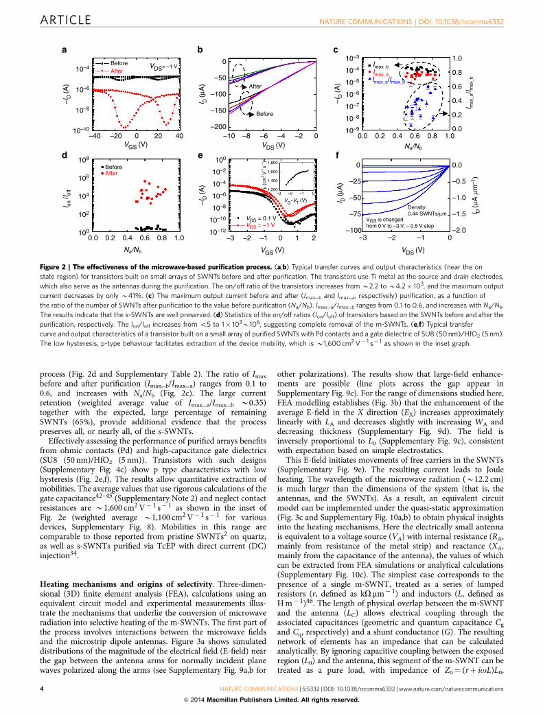
process (Fig. 2d and Supplementary Table 2). The ratio of Imax
before and after purification (Imax_b/Imax_a) ranges from 0.1 to0.6, and increases with Na/Nb (Fig. 2c). The large currentretention (weighted average value of Imax_a/Imax_b B0.35)together with the expected, large percentage of remainingSWNTs (65%), provide additional evidence that the processpreserves all, or nearly all, of the s-SWNTs.
Effectively assessing the performance of purified arrays benefitsfrom ohmic contacts (Pd) and high-capacitance gate dielectrics(SU8 (50 nm)/HfO2 (5 nm)). Transistors with such designs(Supplementary Fig. 4c) show p type characteristics with lowhysteresis (Fig. 2e,f). The results allow quantitative extraction ofmobilities. The average values that use rigorous calculations of thegate capacitance42–45 (Supplementary Note 2) and neglect contactresistances are B1,600 cm2 V 1 s 1 as shown in the inset ofFig. 2e (weighted average B1,100 cm2 V 1 s 1 for variousdevices, Supplementary Fig. 8). Mobilities in this range arecomparable to those reported from pristine SWNTs2 on quartz,as well as s-SWNTs purified via TcEP with direct current (DC)injection34.
Heating mechanisms and origins of selectivity. Three-dimen-sional (3D) finite element analysis (FEA), calculations using anequivalent circuit model and experimental measurements illus-trate the mechanisms that underlie the conversion of microwaveradiation into selective heating of the m-SWNTs. The first part ofthe process involves interactions between the microwave fieldsand the microstrip dipole antennas. Figure 3a shows simulateddistributions of the magnitude of the electrical field (E-field) nearthe gap between the antenna arms for normally incident planewaves polarized along the arms (see Supplementary Fig. 9a,b for
other polarizations). The results show that large-field enhance-ments are possible (line plots across the gap appear inSupplementary Fig. 9c). For the range of dimensions studied here,FEA modelling establishes (Fig. 3b) that the enhancement of theaverage E-field in the X direction (EX) increases approximatelylinearly with LA and decreases slightly with increasing WA anddecreasing thickness (Supplementary Fig. 9d). The field isinversely proportional to L0 (Supplementary Fig. 9c), consistentwith expectation based on simple electrostatics.
This E-field initiates movements of free carriers in the SWNTs(Supplementary Fig. 9e). The resulting current leads to Jouleheating. The wavelength of the microwave radiation (B12.2 cm)is much larger than the dimensions of the system (that is, theantennas, and the SWNTs). As a result, an equivalent circuitmodel can be implemented under the quasi-static approximation(Fig. 3c and Supplementary Fig. 10a,b) to obtain physical insightsinto the heating mechanisms. Here the electrically small antennais equivalent to a voltage source (VA) with internal resistance (RA,mainly from resistance of the metal strip) and reactance (XA,mainly from the capacitance of the antenna), the values of whichcan be extracted from FEA simulations or analytical calculations(Supplementary Fig. 10c). The simplest case corresponds to thepresence of a single m-SWNT, treated as a series of lumpedresistors (r, defined as kOmm 1) and inductors (L, defined asH m 1)46. The length of physical overlap between the m-SWNTand the antenna (LC) allows electrical coupling through theassociated capacitances (geometric and quantum capacitance Cg
and Cq, respectively) and a shunt conductance (G). The resultingnetwork of elements has an impedance that can be calculatedanalytically. By ignoring capacitive coupling between the exposedregion (L0) and the antenna, this segment of the m-SWNT can betreated as a pure load, with impedance of Z0¼ (rþ ioL)L0,
10–4After
After
Before
AfterBefore
Before
10–6
10–8
108 100
10–2
10–4
10–6–l
D (A
)
–lD
(A)
l on
/l off
VGS (V)
VDS= –1 V
VG-VT (V)
μ (c
m2 V
–1s–1
)
VDS (V)
VDS = 0.1 VVDS = –1 V
VGS (V) VDS (V)Na/Nb
Na/Nb
–lD
(A)
l D (μ
A)
l D (μ
A)
l D (μ
A μ
m–1
)
10–8
10–10
10–12
106
104
102
100
10–3
10–4
10–5
10–6
10–7
10–8
10–90.0 0.2 0.4 0.6 0.8 1.0
0.0
0.0
–0.5
–1.0
–1.5
–2.0
0.2
0.4
0.6
0.8
1.0
10–10–40
0.0 0.2 0.4 0.6 0.8 1.0
–200–10
–3 –3–100
–75
–50
–25
0
–2 –2–1 –110 02
–8 –6 –4 –2
–31,200
1,400
1,600
1,800
–2 –1 0
0
–150
–100
–50
0
–20 20 400
Imax_bImax_aImax_a/Imax_b
I max
_a/I m
ax_b
Density:0.44 SWNTs/μm
VGS is changedfrom 0 V to –3 V, – 0.5 V step
Figure 2 | The effectiveness of the microwave-based purification process. (a,b) Typical transfer curves and output characteristics (near the on
state region) for transistors built on small arrays of SWNTs before and after purification. The transistors use Ti metal as the source and drain electrodes,
which also serve as the antennas during the purification. The on/off ratio of the transistors increases from B2.2 to B4.2 103, and the maximum output
current decreases by only B41%. (c) The maximum output current before and after (Imax_b and Imax_a, respectively) purification, as a function of
the ratio of the number of SWNTs after purification to the value before purification (Na/Nb). Imax_a/Imax_b ranges from 0.1 to 0.6, and increases with Na/Nb.
The results indicate that the s-SWNTs are well preserved. (d) Statistics of the on/off ratios (Ion/Ioff) of transistors based on the SWNTs before and after the
purification, respectively. The Ion/Ioff increases from o5 to 1 103B106, suggesting complete removal of the m-SWNTs. (e,f) Typical transfer
curve and output characteristics of a transistor built on a small array of purified SWNTs with Pd contacts and a gate dielectric of SU8 (50 nm)/HfO2 (5 nm).
The low hysteresis, p-type behaviour facilitates extraction of the device mobility, which is B1,600 cm2 V 1 s 1 as shown in the inset graph.
ARTICLE NATURE COMMUNICATIONS | DOI: 10.1038/ncomms6332
4 NATURE COMMUNICATIONS | 5:5332 | DOI: 10.1038/ncomms6332 | www.nature.com/naturecommunications
& 2014 Macmillan Publishers Limited. All rights reserved.
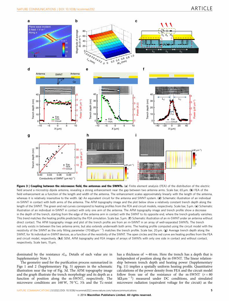
dominated by the resistance rL0. Details of each value are inSupplementary Note 3.
The geometry used for the purification process summarized inFigs 1 and 2 (Supplementary Fig. 5) appears in the schematicillustration near the top of Fig. 3d. The AFM topography imageand the graph illustrate the trench morphology and its depth as afunction of position along the m-SWNT, respectively. Themicrowave conditions are 160 W, 70 C, 3 h and the Tc-resist
has a thickness of B40 nm. Here the trench has a depth that isindependent of position along the m-SWNT. The linear relation-ship between trench depth and heating power (SupplementaryFig. 11) implies a spatially uniform heating profile. Quantitativecalculations of the power density from FEA and the circuit modelfollow from use of the resistance of the m-SWNT (r¼ 80kOmm 1) measured under DC conditions, and simulatedmicrowave radiation (equivalent voltage for the circuit) as the
40
30
20
Tren
ch d
epth
(nm
)
Pow
er (
μW μ
m–1
)
Pow
er (
μW μ
m–1
)
Pow
er (
A.U
)
10Exp.
Exp.FEA.FEA.
Exp.
L0
LCLC
CircuitCircuit
–10 –5 0 5X (μm)
10 –10 –5 0 5X (μm) X (μm)
10 4020–20–40 0
0
40
Antenna Antenna
30V m–1
Plane wave incident
80
60
Mag
nitu
de o
f ave
rage
Ex
(V m
–1)
40
20
01.0 0.8 0.6 0.4 0.20
LA (mm)
E-field: 1 V m–1
Along x
Z
XY
20
10
0
QzX
Z
SWNT
30
20
Tren
ch d
epth
(nm
)
10
0
404
303
202
Tren
ch d
epth
(nm
)
101
00
4
3
2
1
0
4
5
3
2
1
0
Pow
er (
μW μ
m–1
)
Exp.FEA.Circuit
000.00 0.03 0.06 0.09
Tren
ch d
epth
(nm
)
1010
2020
3030
Conductivity of SWNT (μm kΩ–1)
4
2
0
4
2
0(μW μm–1)
(μW μm–1)
Antenna area
Antenna area
WA (mm)
0 0.2 0.4 0.6 0.8 1.0
CgCq
L r RC
LC
VA XA RA
LCL0
Figure 3 | Coupling between the microwave field, the antennas and the SWNTs. (a) Finite element analysis (FEA) of the distribution of the electric
field around a microstrip dipole antenna, revealing a strong enhancement near the gap between two antenna arms. Scale bar, 65 mm. (b) FEA of the
field enhancement as a function of the length and width of the antenna. The enhancement scales approximately linearly with the length of the antenna,
whereas it is relatively insensitive to the width. (c) An equivalent circuit for the antenna and SWNT system. (d) Schematic illustration of an individual
m-SWNT in contact with both arms of the antenna. The AFM topography image and the plot below show a relatively constant trench depth along the
length of the SWNT. The green and red curves correspond to heating profiles from the FEA and circuit models, respectively. Scale bar, 5mm. (e) Schematic
illustration of an individual m-SWNT in contact with only one arm of the antenna. The AFM topography image and trench profile show a decrease
in the depth of the trench, starting from the edge of the antenna arm in contact with the SWNT to its opposite end, where the trench gradually vanishes.
This trend matches the heating profile predicted by the FEA simulation. Scale bar, 5 mm. (f) Schematic illustration of an m-SWNT under an antenna without
direct contact. The AFM topography image and plot of the trench profile are from an m-SWNT in an array of well-separated SWNTs. The trench
not only exists in between the two antenna arms, but also extends underneath both arms. The heating profile computed using the circuit model with the
resistivity of the SWNT as the only fitting parameter (70 kOmm 1) matches the trench profile. Scale bar, 20mm. (g) Average trench depth along the
SWNT, for 16 individual m-SWNT devices, as a function of the resistivity of the SWNT. The open circles and the red curve are heating profiles from the FEA
and circuit model, respectively. (h,i) SEM, AFM topography and FEA images of arrays of SWNTs with only one side in contact and without contact,
respectively. Scale bars, 15mm.
NATURE COMMUNICATIONS | DOI: 10.1038/ncomms6332 ARTICLE
NATURE COMMUNICATIONS | 5:5332 | DOI: 10.1038/ncomms6332 | www.nature.com/naturecommunications 5
& 2014 Macmillan Publishers Limited. All rights reserved.
source (Supplementary Fig. 12). The DC value of r provides agood approximation of the corresponding AC value because otoo1, where t (B10 12 s)38 is the characteristic scattering timein SWNTs and o is the angular frequency of the microwaves(2p 2.45 GHz). The simulations show a nearly constant heatingprofile, consistent with experimental observations of the trenchdepth. Based on the similarity in flow profiles, the temperatureincrease associated with microwave irradiation can be assumed tobe similar to that associated with DC injection reportedpreviously34. Microwave heating power densities between 3 and30 W m 1, therefore, correspond to temperature increases at thetop-surface of Tc-resist of between 2 and 15 C (ref. 34).
In rare cases, the SWNTs make contact only to one side of theantenna, as shown in the Fig. 3e. The corresponding AFMtopography image and profile of the trench depth associated witha m-SWNT in this type of configuration (metallic type inferredfrom the formation of the trench; Tc-resist B40 nm; microwaveconditions: 300 W, 70 C, 3 h) reveal a spatial decrease in depth,starting from the edge of the antenna arm that contacts them-SWNT and extending continuously to its tip end. This trendmatches the heating profiles calculated by FEA, as shown here inarbitrary units (The profile is nearly invariant with r, for valuesbetween 10 and 100 kOmm 1.). This behaviour indicates that thecurrent flow in the SWNT decreases continuously to zero at thetip, as required by the boundary conditions at that location.Another case of interest, as described subsequently, occurs whenthe SWNTs span the gap but do not directly contact the antenna,as shown in Fig. 3f. Here only capacitive coupling is important.The AFM topography image and trench depth correspond to am-SWNT (determined by Raman microscopy) in a sparse array(distances from adjacent SWNTs 43 mm) on a sapphire substrateto facilitate Raman measurements47 (Supplementary Note 4 andSupplementary Fig. 13). Here microwave exposure (160 W, 70 C,3 h) occurs, while antennas (LA¼ 1,000 mm, WA¼ 80mm andL0¼ 8mm) on a cover glass are separated by a B1.1-mm air gapabove the SWNTs (see Methods). The results show that thetrench depth is largest at the centre region (L0) and graduallydecreases to zero within a distance shorter than the overlap length(LC). With r¼ 70 kOmm 1, the circuit model yields a spatialvariation in heating power that matches the observed trenchdepth (Fig. 3f). These variations take the form of |sinh2(x/LT)|,
where LT ffiffiffiffiffiffiffiffiffiffiffiffiffiffiffiffiffiffiffiffiffiffiffiffiffiffiffiffiffiffiffiffiffiffiffiffiffiffi
1=Cgþ 1=Cq
=iorq
is the transfer length
(magnitude B9.5 mm in this case, Supplementary Note 3). Asthe capacitive coupling mechanism does not require the antennasto contact the SWNTs, it provides an interesting option inpurification, as described subsequently. On the other hand, directcontact offers significant benefits in selectivity, also as describedsubsequently.
By comparison to individual SWNTs, implementation witharrays involves additional considerations related to wide varia-tions in the electrical properties of the SWNTs48,49 (chiralities,resistivities) and coupling (electrical, thermal, flow) betweenthem. The circuit model treats each SWNT (the centre part withlength L0) as a load with impedance Z0, which is dominated bythe resistance of the SWNT. Experimental validation of thisapproach can be accomplished through studies of trenchesformed in isolated SWNTs with different resistances. The antennasfor these measurements use the structure in Supplementary Fig. 5with Ti (2 nm)/Pd (48 nm) and L0¼B8mm. The experimentsinvolve Tc-resist with thickness of B50 nm, and microwaveconditions of 80 W, 60 C and 3 h. Figure 3g plots the averagetrench depth formed with 16 different m-SWNTs as a function oftheir conductivity evaluated at a bias of 1 V (SupplementaryFig. 14). The linear relationship is consistent with a dominant roleof the load impedance, as in the FEA simulation and the
equivalent circuit model. Arrays of SWNTs can be viewed asindividual SWNTs, electrically connected in parallel. Figure 3h,ishows results obtained with arrays (160 W, 70 C, 3 h, Tc-resistthicknessB40 nm) for the cases of contact on one side and for nocontact with the antennas, respectively (contacts on both sidesappears in Fig. 1b). The depths of the trenches are different foreach of the SWNTs, likely due to variations in their conductances,per results of Fig. 3g. FEA simulations of the heating power alongthe lengths of the SWNTs provide some insights. Here the FEAmodelling treats the SWNTs as uniform resistors, with overallmagnitudes that incorporate the contact effects (quantum contactresistances and Schottky barriers at the contacts) in an ad hocmanner. Quantitative treatments using 1D drift diffusion models,described subsequently, capture the detailed physics of thesebarriers. The results in Fig. 3h include 7 SWNTs with a small r(53.3 kOmm 1, derived from the total resistance measured onthe entire array before isolation from one contact), and 15SWNTs with large r (5,330 kOmm 1 to represent the SWNTsthat do not form trenches17,50). The magnitudes of the computedpower inside each SWNT in the array are directly related to thevalues of r. For this particular geometry, SWNT–SWNT coupling,although present44, does not have a significant effect on theresults. The non-contact case (Fig. 3i) also shows a distributionof trench depths. Here assignments of SWNTs with variousresistivity (50 kOmm 1 to represent the most conductingSWNTs37; 150 kOmm 1 to represent moderate conductingones51; 5,000 kOmm 1 to represent the least conductingones50) in the FEA allow correlation of the conductances of theSWNTs with the magnitudes of heating, as also expected from theequivalent circuit results.
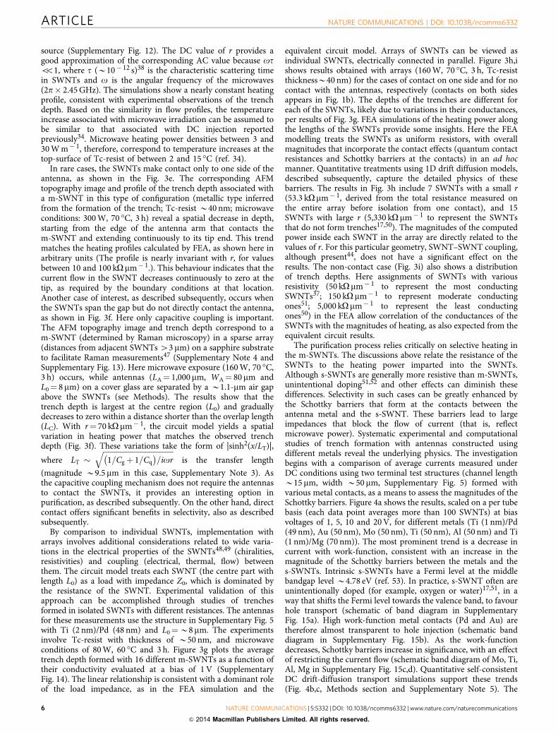
The purification process relies critically on selective heating inthe m-SWNTs. The discussions above relate the resistance of theSWNTs to the heating power imparted into the SWNTs.Although s-SWNTs are generally more resistive than m-SWNTs,unintentional doping51,52 and other effects can diminish thesedifferences. Selectivity in such cases can be greatly enhanced bythe Schottky barriers that form at the contacts between theantenna metal and the s-SWNT. These barriers lead to largeimpedances that block the flow of current (that is, reflectmicrowave power). Systematic experimental and computationalstudies of trench formation with antennas constructed usingdifferent metals reveal the underlying physics. The investigationbegins with a comparison of average currents measured underDC conditions using two terminal test structures (channel lengthB15 mm, width B50 mm, Supplementary Fig. 5) formed withvarious metal contacts, as a means to assess the magnitudes of theSchottky barriers. Figure 4a shows the results, scaled on a per tubebasis (each data point averages more than 100 SWNTs) at biasvoltages of 1, 5, 10 and 20 V, for different metals (Ti (1 nm)/Pd(49 nm), Au (50 nm), Mo (50 nm), Ti (50 nm), Al (50 nm) and Ti(1 nm)/Mg (70 nm)). The most prominent trend is a decrease incurrent with work-function, consistent with an increase in themagnitude of the Schottky barriers between the metals and thes-SWNTs. Intrinsic s-SWNTs have a Fermi level at the middlebandgap level B4.78 eV (ref. 53). In practice, s-SWNT often areunintentionally doped (for example, oxygen or water)17,51, in away that shifts the Fermi level towards the valence band, to favourhole transport (schematic of band diagram in SupplementaryFig. 15a). High work-function metal contacts (Pd and Au) aretherefore almost transparent to hole injection (schematic banddiagram in Supplementary Fig. 15b). As the work-functiondecreases, Schottky barriers increase in significance, with an effectof restricting the current flow (schematic band diagram of Mo, Ti,Al, Mg in Supplementary Fig. 15c,d). Quantitative self-consistentDC drift-diffusion transport simulations support these trends(Fig. 4b,c, Methods section and Supplementary Note 5). The
ARTICLE NATURE COMMUNICATIONS | DOI: 10.1038/ncomms6332
6 NATURE COMMUNICATIONS | 5:5332 | DOI: 10.1038/ncomms6332 | www.nature.com/naturecommunications
& 2014 Macmillan Publishers Limited. All rights reserved.
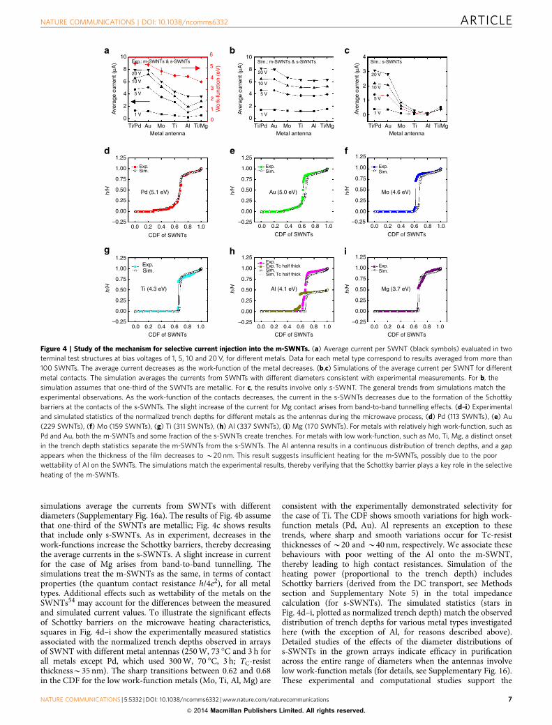
simulations average the currents from SWNTs with differentdiameters (Supplementary Fig. 16a). The results of Fig. 4b assumethat one-third of the SWNTs are metallic; Fig. 4c shows resultsthat include only s-SWNTs. As in experiment, decreases in thework-functions increase the Schottky barriers, thereby decreasingthe average currents in the s-SWNTs. A slight increase in currentfor the case of Mg arises from band-to-band tunnelling. Thesimulations treat the m-SWNTs as the same, in terms of contactproperties (the quantum contact resistance h/4e2), for all metaltypes. Additional effects such as wettability of the metals on theSWNTs54 may account for the differences between the measuredand simulated current values. To illustrate the significant effectsof Schottky barriers on the microwave heating characteristics,squares in Fig. 4d–i show the experimentally measured statisticsassociated with the normalized trench depths observed in arraysof SWNT with different metal antennas (250 W, 73 C and 3 h forall metals except Pd, which used 300 W, 70 C, 3 h; TC-resistthicknessB35 nm). The sharp transitions between 0.62 and 0.68in the CDF for the low work-function metals (Mo, Ti, Al, Mg) are
consistent with the experimentally demonstrated selectivity forthe case of Ti. The CDF shows smooth variations for high work-function metals (Pd, Au). Al represents an exception to thesetrends, where sharp and smooth variations occur for Tc-resistthicknesses of B20 and B40 nm, respectively. We associate thesebehaviours with poor wetting of the Al onto the m-SWNT,thereby leading to high contact resistances. Simulation of theheating power (proportional to the trench depth) includesSchottky barriers (derived from the DC transport, see Methodssection and Supplementary Note 5) in the total impedancecalculation (for s-SWNTs). The simulated statistics (stars inFig. 4d–i, plotted as normalized trench depth) match the observeddistribution of trench depths for various metal types investigatedhere (with the exception of Al, for reasons described above).Detailed studies of the effects of the diameter distributions ofs-SWNTs in the grown arrays indicate efficacy in purificationacross the entire range of diameters when the antennas involvelow work-function metals (for details, see Supplementary Fig. 16).These experimental and computational studies support the
10
8
6
4
2
0
10
8
6
4
2
0
–0.250.0 0.2 0.4
CDF of SWNTs
0.6 0.8 1.0 0.0 0.2 0.4
CDF of SWNTs
0.6 0.8 1.0 0.0 0.2 0.4
CDF of SWNTs
0.6 0.8 1.0
0.0 0.2 0.4
CDF of SWNTs
0.6 0.8 1.0 0.0 0.2 0.4
CDF of SWNTs
0.6 0.8 1.0 0.0 0.2 0.4
CDF of SWNTs
0.6 0.8 1.0
0.00
0.50
h/H
h/H
h/H
h/H
h/H
h/H
0.25
1.00
1.25
Metal antennaTi/Pd Ti AlAu Mo Ti/Mg
Metal antennaTi/Pd Ti AlAu Mo Ti/Mg
Metal antennaTi/Pd
Ave
rage
cur
rent
(μA
)
Ave
rage
cur
rent
(μA
)
Wor
k-fu
nctio
n (e
V)
Ave
rage
cur
rent
(μA
)
Ti AlAu Mo Ti/Mg
Exp.Sim.
Pd (5.1 eV)
Exp.Sim.
Au (5.0 eV)
Exp.
20 V
10 V
5 V
1 V
20 V
10 V
5 V
1 V
20 V
10 V
5 V
1 V
Sim.: s-SWNTsSim.: m-SWNTs & s-SWNTsExp.: m-SWNTs & s-SWNTs
Sim.
Mo (4.6 eV)
Exp.Sim.
Mg (3.7 eV)Al (4.1 eV)Ti (4.3 eV)
Exp.Exp. Exp. Tc half thick
Sim. Tc half thickSim.Sim.
0.75
–0.25
0.00
0.50
0.25
1.00
1.25
0.75
–0.25
0.00
0.50
0.25
1.00
1.25
0.75
–0.25
0.00
0.50
0.25
1.00
1.25
0.75
–0.25
0.00
0.50
0.25
1.00
1.25
0.75
–0.25
0.00
0.50
0.25
1.00
1.25
0.75
4
3
0
1
2
4
5
6
3
0
1
2
Figure 4 | Study of the mechanism for selective current injection into the m-SWNTs. (a) Average current per SWNT (black symbols) evaluated in two
terminal test structures at bias voltages of 1, 5, 10 and 20 V, for different metals. Data for each metal type correspond to results averaged from more than
100 SWNTs. The average current decreases as the work-function of the metal decreases. (b,c) Simulations of the average current per SWNT for different
metal contacts. The simulation averages the currents from SWNTs with different diameters consistent with experimental measurements. For b, the
simulation assumes that one-third of the SWNTs are metallic. For c, the results involve only s-SWNT. The general trends from simulations match the
experimental observations. As the work-function of the contacts decreases, the current in the s-SWNTs decreases due to the formation of the Schottky
barriers at the contacts of the s-SWNTs. The slight increase of the current for Mg contact arises from band-to-band tunnelling effects. (d–i) Experimental
and simulated statistics of the normalized trench depths for different metals as the antennas during the microwave process, (d) Pd (113 SWNTs), (e) Au
(229 SWNTs), (f) Mo (159 SWNTs), (g) Ti (311 SWNTs), (h) Al (337 SWNTs), (i) Mg (170 SWNTs). For metals with relatively high work-function, such as
Pd and Au, both the m-SWNTs and some fraction of the s-SWNTs create trenches. For metals with low work-function, such as Mo, Ti, Mg, a distinct onset
in the trench depth statistics separate the m-SWNTs from the s-SWNTs. The Al antenna results in a continuous distribution of trench depths, and a gap
appears when the thickness of the film decreases to B20 nm. This result suggests insufficient heating for the m-SWNTs, possibly due to the poor
wettability of Al on the SWNTs. The simulations match the experimental results, thereby verifying that the Schottky barrier plays a key role in the selective
heating of the m-SWNTs.
NATURE COMMUNICATIONS | DOI: 10.1038/ncomms6332 ARTICLE
NATURE COMMUNICATIONS | 5:5332 | DOI: 10.1038/ncomms6332 | www.nature.com/naturecommunications 7
& 2014 Macmillan Publishers Limited. All rights reserved.
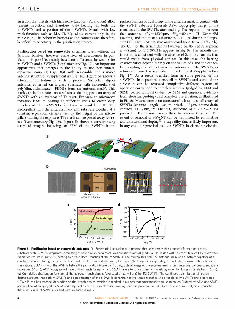
assertion that metals with high work-function (Pd and Au) allowcurrent injection, and therefore Joule heating, in both them-SWNTs and a portion of the s-SWNTs. Metals with lowwork-function such as Mo, Ti, Mg, allow current only in them-SWNTs. The Schottky barriers at the contacts are, therefore,beneficial to selectivity in the purification process.
Purification based on removable antennas. Even without theSchottky barriers, however, some level of effectiveness in pur-ification is possible, mainly based on differences between r form-SWNTs and s-SWNTs (Supplementary Fig. 17). An importantopportunity that emerges is the ability to use non-contact,capacitive coupling (Fig. 3f,i) with removable and reusableantenna structures (Supplementary Fig. 18). Figure 5a shows aschematic illustration of such a process. Microstrip dipoleantennas patterned on a glass substrate with micropillars ofpoly(dimethylsiloxane) (PDMS) form an ‘antenna mask’. Thismask can be laminated on a substrate that supports an array ofSWNTs with an overcoat of Tc-resist. Exposure to microwaveradiation leads to heating at sufficient levels to create deeptrenches at the m-SWNTs for their removal by RIE. Themicropillars hold the antenna mask and substrate together at aconstant separation distance (set by the height of the micro-pillars) during the exposure. The mask can be peeled away for re-use (Supplementary Fig. 19). Figure 5b shows a correspondingseries of images, including an SEM of the SWNTs before
purification; an optical image of the antenna mask in contact withthe SWNT substrate (quartz); AFM topography image of thetrenches and the SWNTs after etching. The separation betweenthe antennas (LA¼ 1,500 mm, WA¼ 80 mm, Ti (2 nm)/Pd(48 nm)) and the quartz substrate is B1.1 mm during the expo-sure (Tc-resist B50 nm; microwave conditions: 80 W, 60 C, 3 h).The CDF of the trench depths (averaged on the centre segmentL0¼ 8 mm) for 112 SWNTs appears in Fig. 5c. The smooth dis-tribution is consistent with the absence of Schottky barriers thatwould result from physical contact. In this case, the heatingcharacteristics depend mainly on the values of r and the capaci-tive coupling strength between the antenna and the SWNTs, asestimated from the equivalent circuit model (SupplementaryFig. 17). As a result, trenches form at some portion of thes-SWNTs. In a practical sense, all m-SWNTs and some of thes-SWNTs can be removed completely; different regions ofoperation correspond to complete removal (judged by AFM andSEM), partial removal (judged by SEM and empirical evidencesfrom electrical probing) and complete preservation, as illustratedin Fig. 5c. Measurements on transistors built using small arrays ofSWNTs (channel length¼ 30 mm, width¼ 35 mm, source-draincontacts Ti (2 nm)/Pd (48 nm), dielectric SU8 2002¼ 2 mm)purified in this manner verify these behaviours (Fig. 5d). Theextent of removal of s-SWNT can be minimized by eliminatingany unintentional doping55, a capability that is likely important,in any case, for practical use of s-SWNTs in electronic circuits.
PDMS pillar
PDMSmicropillars
Antenna
Antenna
Marker on thereceiving substrate
Full elimination
Partial damage
Full preservation
0.0 0.2 0.4 0.6 0.8
CDF of SWNTs–90
10–12
10–11
10–10
10–9
10–8
10–7
10–6
–60 –30 30
VGS (V)
–ID(A
)
60 900
h (n
m)
1.0
Antenna area
Antenna area
Antenna
Antenna
E
H
50
40
30
20
10
0
Figure 5 | Purification based on removable antennas. (a) Schematic illustration of a process that uses removable antennas formed on a glass
substrate with PDMS micropillars. Laminating this type of antenna mask on a substrate with aligned SWNTs coated with Tc-resist, followed by microwave
irradiation results in sufficient heating to create deep trenches at the m-SWNTs. The micropillars hold the antenna mask and substrate together at a
constant distance during the process. The mask can be removed afterward, for reuse. (b) Images corresponding to each step shown in the schematic
illustrations: SEM image of the SWNTs before the purification (scale bar, 15 mm); optical image of the antenna mask after contacting the quartz substrate
(scale bar, 50mm); AFM topography image of the trench formation and SEM image after the etching and washing away the Tc-resist (scale bars, 15 mm).
(c) Cumulative distribution function of the average trench depths (averaged on L0¼8 mm) for 112 SWNTs. The continuous distribution of trench
depths suggests that both m-SWNTs and some fraction of the s-SWNTs generate heat to create trenches. As a result, all m-SWNTs and a portion of
s-SWNTs can be removed, depending on the trench depths, which are marked in regions that correspond to full elimination (judged by AFM and SEM),
partial elimination (judged by SEM and empirical evidence from electrical probing) and full preservation. (d) Transfer curve from a typical transistor
that uses arrays of SWNTs purified with an antenna mask.
ARTICLE NATURE COMMUNICATIONS | DOI: 10.1038/ncomms6332
8 NATURE COMMUNICATIONS | 5:5332 | DOI: 10.1038/ncomms6332 | www.nature.com/naturecommunications
& 2014 Macmillan Publishers Limited. All rights reserved.
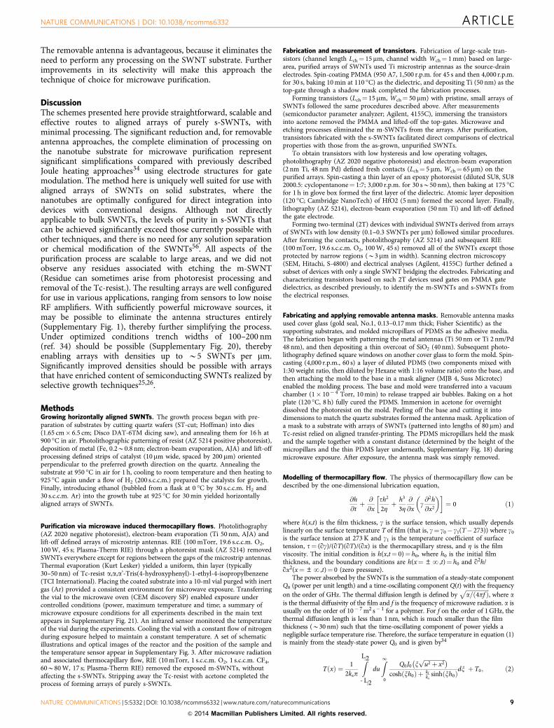
The removable antenna is advantageous, because it eliminates theneed to perform any processing on the SWNT substrate. Furtherimprovements in its selectivity will make this approach thetechnique of choice for microwave purification.
DiscussionThe schemes presented here provide straightforward, scalable andeffective routes to aligned arrays of purely s-SWNTs, withminimal processing. The significant reduction and, for removableantenna approaches, the complete elimination of processing onthe nanotube substrate for microwave purification representsignificant simplifications compared with previously describedJoule heating approaches34 using electrode structures for gatemodulation. The method here is uniquely well suited for use withaligned arrays of SWNTs on solid substrates, where thenanotubes are optimally configured for direct integration intodevices with conventional designs. Although not directlyapplicable to bulk SWNTs, the levels of purity in s-SWNTs thatcan be achieved significantly exceed those currently possible withother techniques, and there is no need for any solution separationor chemical modification of the SWNTs56. All aspects of thepurification process are scalable to large areas, and we did notobserve any residues associated with etching the m-SWNT(Residue can sometimes arise from photoresist processing andremoval of the Tc-resist.). The resulting arrays are well configuredfor use in various applications, ranging from sensors to low noiseRF amplifiers. With sufficiently powerful microwave sources, itmay be possible to eliminate the antenna structures entirely(Supplementary Fig. 1), thereby further simplifying the process.Under optimized conditions trench widths of 100–200 nm(ref. 34) should be possible (Supplementary Fig. 20), therebyenabling arrays with densities up to B5 SWNTs per mm.Significantly improved densities should be possible with arraysthat have enriched content of semiconducting SWNTs realized byselective growth techniques25,26.
MethodsGrowing horizontally aligned SWNTs. The growth process began with pre-paration of substrates by cutting quartz wafers (ST-cut; Hoffman) into dies(1.65 cm 6.5 cm; Disco DAT-6TM dicing saw), and annealing them for 16 h at900 C in air. Photolithographic patterning of resist (AZ 5214 positive photoresist),deposition of metal (Fe, 0.2B0.8 nm; electron-beam evaporation, AJA) and lift-offprocessing defined strips of catalyst (10 mm wide, spaced by 200 mm) orientedperpendicular to the preferred growth direction on the quartz. Annealing thesubstrate at 950 C in air for 1 h, cooling to room temperature and then heating to925 C again under a flow of H2 (200 s.c.c.m.) prepared the catalysts for growth.Finally, introducing ethanol (bubbled from a flask at 0 C by 30 s.c.c.m. H2 and30 s.c.c.m. Ar) into the growth tube at 925 C for 30 min yielded horizontallyaligned arrays of SWNTs.
Purification via microwave induced thermocapillary flows. Photolithography(AZ 2020 negative photoresist), electron-beam evaporation (Ti 50 nm, AJA) andlift-off defined arrays of microstrip antennas. RIE (100 mTorr, 19.6 s.c.c.m. O2,100 W, 45 s; Plasma-Therm RIE) through a photoresist mask (AZ 5214) removedSWNTs everywhere except for regions between the gaps of the microstrip antennas.Thermal evaporation (Kurt Lesker) yielded a uniform, thin layer (typically30–50 nm) of Tc-resist a,a,a’-Tris(4-hydroxyphenyl)-1-ethyl-4-isopropylbenzene(TCI International). Placing the coated substrate into a 10-ml vial purged with inertgas (Ar) provided a consistent environment for microwave exposure. Transferringthe vial to the microwave oven (CEM discovery SP) enabled exposure undercontrolled conditions (power, maximum temperature and time; a summary ofmicrowave exposure conditions for all experiments described in the main textappears in Supplementary Fig. 21). An infrared sensor monitored the temperatureof the vial during the experiments. Cooling the vial with a constant flow of nitrogenduring exposure helped to maintain a constant temperature. A set of schematicillustrations and optical images of the reactor and the position of the sample andthe temperature sensor appear in Supplementary Fig. 3. After microwave radiationand associated thermocapillary flow, RIE (10 mTorr, 1 s.c.c.m. O2, 1 s.c.c.m. CF4,60B80 W, 17 s; Plasma-Therm RIE) removed the exposed m-SWNTs, withoutaffecting the s-SWNTs. Stripping away the Tc-resist with acetone completed theprocess of forming arrays of purely s-SWNTs.
Fabrication and measurement of transistors. Fabrication of large-scale tran-sistors (channel length Lch¼ 15mm, channel width Wch¼ 1 mm) based on large-area, purified arrays of SWNTs used Ti microstrip antennas as the source-drainelectrodes. Spin-coating PMMA (950 A7, 1,500 r.p.m. for 45 s and then 4,000 r.p.m.for 30 s, baking 10 min at 110 C) as the dielectric, and depositing Ti (50 nm) as thetop-gate through a shadow mask completed the fabrication processes.
Forming transistors (Lch¼ 15 mm, Wch¼ 50mm) with pristine, small arrays ofSWNTs followed the same procedures described above. After measurements(semiconductor parameter analyzer; Agilent, 4155C), immersing the transistorsinto acetone removed the PMMA and lifted-off the top-gates. Microwave andetching processes eliminated the m-SWNTs from the arrays. After purification,transistors fabricated with the s-SWNTs facilitated direct comparisons of electricalproperties with those from the as-grown, unpurified SWNTs.
To obtain transistors with low hysteresis and low operating voltages,photolithography (AZ 2020 negative photoresist) and electron-beam evaporation(2 nm Ti, 48 nm Pd) defined fresh contacts (Lch¼ 5 mm, Wch¼ 65mm) on thepurified arrays. Spin-casting a thin layer of an epoxy photoresist (diluted SU8, SU82000.5: cyclopentanone¼ 1:7; 3,000 r.p.m. for 30 sB50 nm), then baking at 175 Cfor 1 h in glove box formed the first layer of the dielectric. Atomic layer deposition(120 C; Cambridge NanoTech) of HfO2 (5 nm) formed the second layer. Finally,lithography (AZ 5214), electron-beam evaporation (50 nm Ti) and lift-off definedthe gate electrode.
Forming two-terminal (2T) devices with individual SWNTs derived from arraysof SWNTs with low density (0.1–0.3 SWNTs per mm) followed similar procedures.After forming the contacts, photolithography (AZ 5214) and subsequent RIE(100 mTorr, 19.6 s.c.c.m. O2, 100 W, 45 s) removed all of the SWNTs except thoseprotected by narrow regions (B3 mm in width). Scanning electron microscopy(SEM, Hitachi, S-4800) and electrical analyses (Agilent, 4155C) further defined asubset of devices with only a single SWNT bridging the electrodes. Fabricating andcharacterizing transistors based on such 2T devices used gates on PMMA gatedielectrics, as described previously, to identify the m-SWNTs and s-SWNTs fromthe electrical responses.
Fabricating and applying removable antenna masks. Removable antenna masksused cover glass (gold seal, No.1, 0.13–0.17 mm thick; Fisher Scientific) as thesupporting substrates, and molded micropillars of PDMS as the adhesive media.The fabrication began with patterning the metal antennas (Ti 50 nm or Ti 2 nm/Pd48 nm), and then depositing a thin overcoat of SiO2 (40 nm). Subsequent photo-lithography defined square windows on another cover glass to form the mold. Spin-casting (4,000 r.p.m., 60 s) a layer of diluted PDMS (two components mixed with1:30 weight ratio, then diluted by Hexane with 1:16 volume ratio) onto the base, andthen attaching the mold to the base in a mask aligner (MJB 4, Suss Microtec)enabled the molding process. The base and mold were transferred into a vacuumchamber (1 10 4 Torr, 10 min) to release trapped air bubbles. Baking on a hotplate (120 C, 8 h) fully cured the PDMS. Immersion in acetone for overnightdissolved the photoresist on the mold. Peeling off the base and cutting it intodimensions to match the quartz substrates formed the antenna mask. Application ofa mask to a substrate with arrays of SWNTs (patterned into lengths of 80mm) andTc-resist relied on aligned transfer-printing. The PDMS micropillars held the maskand the sample together with a constant distance (determined by the height of themicropillars and the thin PDMS layer underneath, Supplementary Fig. 18) duringmicrowave exposure. After exposure, the antenna mask was simply removed.
Modelling of thermocapillary flow. The physics of thermocapillary flow can bedescribed by the one-dimensional lubrication equation,
@h@tþ @
@xth2
2Zþ h3
3Z@
@xg@2h@x2
¼ 0 ð1Þ
where h(x,t) is the film thickness, g is the surface tension, which usually dependslinearly on the surface temperature T of film (that is, g¼ g0 g1(T 273)) where g0
is the surface tension at 273 K and g1 is the temperature coefficient of surfacetension, t¼ (qg)/(qT)(qT)/(qx) is the thermocapillary stress, and Z is the filmviscosity. The initial condition is h(x,t¼ 0)¼ h0, where h0 is the initial filmthickness, and the boundary conditions are h(x¼±N,t)¼ h0 and q2h/qx2(x¼±N,t)¼ 0 (zero pressure).
The power absorbed by the SWNTs is the summation of a steady-state componentQ0 (power per unit length) and a time-oscillating component Q(t) with the frequencyon the order of GHz. The thermal diffusion length is defined by
ffiffiffiffiffiffiffiffiffiffiffiffiffiffiffiffia= 4pfð Þ
p, where a
is the thermal diffusivity of the film and f is the frequency of microwave radiation. a isusually on the order of 10 7 m2 s 1 for a polymer. For f on the order of 1 GHz, thethermal diffusion length is less than 1 nm, which is much smaller than the filmthickness (B30 nm) such that the time-oscillating component of power yields anegligible surface temperature rise. Therefore, the surface temperature in equation (1)is mainly from the steady-state power Q0 and is given by34
TðxÞ ¼ 12ksp
ZL=2
- L=2
duZ1
0
Q0J0 xffiffiffiffiffiffiffiffiffiffiffiffiffiffiffiu2 þ x2p
cosh xh0ð Þþ kfks
sinh xh0ð Þdx þT0; ð2Þ
NATURE COMMUNICATIONS | DOI: 10.1038/ncomms6332 ARTICLE
NATURE COMMUNICATIONS | 5:5332 | DOI: 10.1038/ncomms6332 | www.nature.com/naturecommunications 9
& 2014 Macmillan Publishers Limited. All rights reserved.
where T0 is the background heating, L is the SWNT length, ks and kf are the thermalconductivity of substrate and film, respectively, and J0 is the 0th order Bessel functionof the first kind. Here kf¼ 0.2 W m 1 K 1 and ks¼ 6 W m 1 K 1 (refs 34,57). Asthe Tc-resist used in the experiment exhibits similar behaviour as polystyrene with amolecular weight 1,215 g mol 1, we take polystyrene’s surface tension with g0 and g1
as 47.4 10 3 N m 1 and 0.078 10 3 N m 1 K 1 (ref. 58), and viscosityZ ¼ 1:3810 4e
1640T 253Pa s, where T has the unit of K, in our calculations. The Fortran
solver PDE_1D_MG can be used to solve equation (1) to yield the evolution of thefilm thickness h(x,t).
FEA of the microwave field distributions. Three-dimensional finite elementsimulations (COMSOL, RF module) yielded distributions of the microwave fieldaround the antennas. Implementation of the scattering field formalism with planewaves (normalized E-field 1 V m 1, polarized along the length of the dipoleantenna) as the background field served as the platform for calculations of indi-vidual antennas. Treating the microstrip antenna and the SWNT with transitionboundaries (thickness 50 nm) simplified the meshing while retaining the essentialphysics. Because of practical constraints in meshing, the SWNTs were modelled as50 or 200 nm wide strips (with resistivity scaled to match the resistance of theSWNTs per unit length). Perfectly matched layers enclosing the simulation domainensured no reflections of the scattered waves. Calculations of antenna arrays uti-lized the perfect electrical conductor and perfect magnetic conductor conditions forthe boundaries perpendicular to the background E-field and M-field, respectively,to guarantee periodicity. Scattering boundary conditions imposed at the upper andlower boundaries absorbed the scattered waves. The calculated E-field (within themiddle gap L0) of the antenna arrays differed by B2% from that of individualantenna for the typical structure (LA¼ 500mm, WA¼ 65mm, L0¼ 15mm, spacingbetween antennas in the array¼ 1,200 mm).
DC transport simulation for different metals as contacts. The average currentand total resistances of the SWNTs are determined by solving self-consistently the3D electrostatics and the 1D drift-diffusion transport through the SWNTs. The 3Delectrostatics accounts of the full device geometry: the SWNTs on the quartzsubstrate are terminated by source (S) and drain (D) contacts, and covered byinsulating material Tc-resist. The results show that carrier transport dependssensitively on (i) the diameter of the tubes within the as-growth array, (ii) thework-function of the contact materials (Pd (5.1 eV), Au (5.0 eV), Mo (4.6 eV), Ti(4.33 eV), Al (4.1 eV), and Mg (3.7 eV))40,54,59 and (iii) effective applied bias, VDS
(extracted by correlating the equivalent trench depths in Tc-resist for DC andmicrowave inputs). The source to drain of this two-terminal device is separated byL0¼ 15mm. These S/D contacts to the s-SWNTs may involve Schottky barriers(work function of the contacto(electron affinityþ band gap) of the s-SWNT) orthey can be ohmic (work function of the contact4(electron affinityþ band gap) ofthe s-SWNT). For the s-SWNTs, irrespective of the contact type, we solve theelectrostatics and charge density self-consistently17,50. We find that for the ohmiccontact, the electrostatic potential drops linearly through the channel, as expected;whereas, for the Schottky contact, the potential drop depends on the contactresistance and a self-consistent solution between electrostatic potential and chargedensity is essential. For low Schottky barriers (related to high work functioncontacts), the current is primarily thermionic; for very high Schottky barriers(related to low work function contacts), the band-bending close to the sourcecontact can be significant enough to induce additional band-to-band tunnellingcurrent50. We note that the model is predictive because each component of themodel has been validated against independent experiments17,50. A detaileddescription of the model follows.
Carrier transport in s-SWNT. The electrostatics potential, V, is a solution ofPoisson equation,
r: erVð Þ ¼ r: ð3Þ
Here the dielectric constant of the medium is e. The charge density, r, is afunction of the density of carriers (electron and hole), and fixed interface charges(4.4 1019 cm 3)17. The fixed charges are determined by fitting the I–Vcharacteristics for one SWNT and subsequently kept constant for all othersimulations involving different diameters and contact work function. The electronand hole concentrations must be calculated as a solution of the continuity and thedrift-diffusion equations, as follows.
1q
dIn
dXRþGSBT;n þGBTBT;n ¼ 0;
1q
dIp
dXþRGSBT;p GBTBT;p ¼ 0: ð4Þ
Where R is the direct band-to-band recombination rate, q is the electron charge,X is the position variable along the SWNTs, and GSBT,n(p) and GBTBT,n(p) are thegeneration rate in the channel for electron (hole) because of Schottky-barriertunnelling and band-to-band tunnelling, respectively, from the source and draincontacts. The expressions for GSBT,n(p) and GBTBT,n(p) along the s-SWNT are
GSBT;n pð ÞðXÞ ¼p dV
dX
ATtdkB
exp 2ffiffiffiffiffi2mp
‘
R X0
ffiffiffiffiffiffiffiffiffiffiffiffiffiffiffiErX;C Vð Þ
pdr
h iln
1þ expZn pð Þ1þ expZn pð Þ;S
h iþ
exp 2ffiffiffiffiffi2mp
‘
R LX
ffiffiffiffiffiffiffiffiffiffiffiffiffiffiffiErX;C Vð Þ
pdr
h iln
1þ expZn pð Þ1þ expZn pð Þ;D
h i24
35; ð5Þ
GBTBT;nðpÞðXÞ ¼59
dV=dXj j2td
p‘ 2vFexp E2
G
d‘ vF dV=dXj j
: ð6Þ
Here A¼ 1.5 102 EGA cm 2 K 2 is the Richardson constant, kB is theBoltzmann constant, T is the lattice temperature and r is a position variable alongthe SWNTs. Effective mass of electron and hole is m¼ EGm0/20, where m0 is themass of free carrier. Zn,S(D)¼ (EF,S(D) EC)/kBT, Zp,S(D)¼ (EV EF,S(D))/kBT,ErX,C¼EC(r)EC(X), ErX,V¼EV(X) EV(r), where EF,S(D) is the Fermi energy forcarriers in S(D) contact. From equation (6), : is the reduced Planck’s constant, t isthe wall thickness of the SWNT, |dV/dX| is the local electric field along SWNT. TheFermi velocity (vF¼ 108 cm s 1) depends the band structure of the SWNTs17. Theband gap of s-SWNTs is related to the diameter of the tubes (d) as EG¼ 0.7/d eVand d is the ideality factor. The drift-diffusion currents for electron (hole), In(p)inequation (4) is represented as,
In ¼ qnmFEdVdXþ qDn
dndX
; Ip ¼ qpmFEdVdX qDp
dpdX
: ð7ÞHere ID¼ Inþ Ip is the current through the s-SWNT. The field-dependent
mobility is mFE¼ mpeak/(1þmpeak|(dV/dX)|/vs), where the peak mobility,mpeak¼ 1,600(300/T)(d/1 nm)2, and vs is the carrier’s saturation velocity60. Dn(p) isthe electron (hole) diffusion coefficient. Additional information includingboundary conditions for Poisson and charge continuity and simulation proceduresis provided in Supplementary Note 5.
Carrier transport in m-SWNT. Regardless the S/D work function, metalliccarbon nanotubes form ohmic contact with source and drain. The electrostaticpotential drops linearly within the channel and charge carriers drift in thispotential profile. The current through the m-SWNT can be calculated asID¼ (4q2/h)(leff/L0)VDS (ref. 38), where leff is the effective mean free path and h isthe Planck’s constant. The parameter leff can be expressed through Mathiessen’srule as leff
1¼ le 1þ lT
1, where le is the elastic scattering mean free path andlT is the distance an electron must travel in the electric field to reach thresholdscattering energy (:O) to emit an optical phonon (:O¼ 0.2 eV) or zone boundaryphonon (:O¼ 0.16 eV)38. Specifically, lT¼ :O/qEX, where EX¼VDS/L0 isthe average electric field along the m-SWNT. The current flow through them-SWNT, therefore, is ID¼ (4q2/h)(leEX/(1þ qleEX/:O)). The elastic scatteringmean free path is proportional to the m-SWNT diameter through the relationle¼ 300 d (ref. 37).
Once we know the current through each s-SWNT and m-SWNT (discussedabove), we calculate the average current for as-grown array SWNTs usingthe diameter distribution obtained from experiments (Supplementary Fig. 7aof ref. 17). The average current for the as-grown array is computed asP
i[ID(i)s SWNT*PDFi*0.67þ ID(i)
m SWNT*PDFi*0.33]/P
i[PDFi*0.67þ PDFi*0.33],where, i is the SWNT index. The average current of an array composed exclusivelyof s-SWNT is
PiID(i)
s SWNT*PDFi/P
iPDFi. We compute the total power dissipationdue to joule heating by integrating of the product of the current and local-fieldalong the SWNT, and assume that the heating and the trench-depth are linearlycorrelated to the power dissipation along the channel. Finally, to differentiatebetween s-SWNTs versus m-SWNTs, we obtain the CDF of diameter distributionof the as-grown array SWNTs by integrating the probability density function(Supplementary Fig. 7a of ref. 17) and normalizing it to 1. We subdivide CDF in a2:1 ratio and assign the corresponding fractions to s-SWNTs (0–67%) andm-SWNTs (68–100%).
References1. Avouris, P., Chen, Z. H. & Perebeinos, V. Carbon-based electronics. Nat.
Nanotech. 2, 605–615 (2007).2. Kang, S. J. et al. High-performance electronics using dense, perfectly aligned
arrays of single-walled carbon nanotubes. Nat. Nanotech. 2, 230–236 (2007).3. Wang, C., Takei, K., Takahashi, T. & Javey, A. Carbon nanotube electronics -
moving forward. Chem. Soc. Rev. 42, 2592–2609 (2013).4. Shulaker, M. M. et al. Carbon nanotube computer. Nature 501, 526–530
(2013).5. Franklin, A. D. et al. Sub-10 nm carbon nanotube transistor. Nano Lett. 12,
758–762 (2012).6. Ding, L. et al. CMOS-based carbon nanotube pass-transistor logic integrated
circuits. Nat. Commun. 3, 677 (2012).7. Franklin, A. D. et al. Carbon nanotube complementary wrap-gate transistors.
Nano Lett. 13, 2490–2495 (2013).8. Zhang, J. et al. Robust digital VLSI using carbon nanotubes. IEEE Trans. CAD
31, 453–471 (2012).9. Park, H. et al. High-density integration of carbon nanotubes via chemical self-
assembly. Nat. Nanotech. 7, 787–791 (2012).10. Choi, S. J. et al. Short-channel transistors constructed with solution-processed
carbon nanotubes. Acs Nano 7, 798–803 (2013).11. Kocabas, C. et al. Radio frequency analog electronics based on carbon nanotube
transistors. Proc. Natl Acad. Sci. USA 105, 1405–1409 (2008).12. Steiner, M. et al. High-frequency performance of scaled carbon nanotube array
field-effect transistors. Appl. Phys. Lett. 101, 053123 (2012).13. Wang, C. et al. Radio frequency and linearity performance of transistors
using high-purity semiconducting carbon nanotubes. Acs Nano 5, 4169–4176(2011).
ARTICLE NATURE COMMUNICATIONS | DOI: 10.1038/ncomms6332
10 NATURE COMMUNICATIONS | 5:5332 | DOI: 10.1038/ncomms6332 | www.nature.com/naturecommunications
& 2014 Macmillan Publishers Limited. All rights reserved.
14. Cao, Q. et al. Arrays of single-walled carbon nanotubes with full surfacecoverage for high-performance electronics. Nat. Nanotech. 8, 180–186 (2013).
15. Nougaret, L. et al. 80 GHz field-effect transistors produced using high puritysemiconducting single-walled carbon nanotubes. Appl. Phys. Lett. 94, 243505(2009).
16. Rutherglen, C., Jain, D. & Burke, P. Nanotube electronics for radiofrequencyapplications. Nat. Nanotech. 4, 811–819 (2009).
17. Xie, X. et al. Electroluminescence in aligned arrays of single-wall carbonnanotubes with asymmetric contacts. Acs Nano 6, 7981–7988 (2012).
18. Avouris, P., Freitag, M. & Perebeinos, V. Carbon-nanotube photonics andoptoelectronics. Nat. Photon. 2, 341–350 (2008).
19. Yang, L. J. et al. Efficient photovoltage multiplication in carbon nanotubes. Nat.Photon. 5, 673–677 (2011).
20. Roberts, M. E., LeMieux, M. C. & Bao, Z. N. Sorted and aligned single-walledcarbon nanotube networks for transistor-based aqueous chemical sensors. AcsNano 3, 3287–3293 (2009).
21. Allen, B. L., Kichambare, P. D. & Star, A. Carbon nanotube field-effect-transistor-based biosensors. Adv. Mater. 19, 1439–1451 (2007).
22. Pengfei, Q. F. et al. Toward large arrays of multiplex functionalized carbonnanotube sensors for highly sensitive and selective molecular detection. NanoLett. 3, 347–351 (2003).
23. Xiao, J. L. et al. Alignment controlled growth of single-walled carbon nanotubeson quartz substrates. Nano Lett. 9, 4311–4319 (2009).
24. Kocabas, C. et al. Guided growth of large-scale, horizontally aligned arrays ofsingle-walled carbon nanotubes and their use in thin-film transistors. Small 1,1110–1116 (2005).
25. Che, Y. C. et al. Selective synthesis and device applications of semiconductingsingle-walled carbon nanotubes using isopropyl alcohol as feedstock. Acs Nano6, 7454–7462 (2012).
26. Jinghua, L. i. et al. Growth of high-density-aligned and semiconducting-enriched single-walled carbon nanotubes decoupling the conflict betweendensity and selectivity. Acs Nano 8, 554–562 (2014).
27. Zhang, G. Y. et al. Selective etching of metallic carbon nanotubes by gas-phasereaction. Science 314, 974–977 (2006).
28. Arnold, M. S., Green, A. A., Hulvat, J. F., Stupp, S. I. & Hersam, M. C. Sortingcarbon nanotubes by electronic structure using density differentiation. Nat.Nanotech. 1, 60–65 (2006).
29. Liu, H. P., Nishide, D., Tanaka, T. & Kataura, H. Large-scale single-chiralityseparation of single-wall carbon nanotubes by simple gel chromatography. Nat.Commun. 2, 309 (2011).
30. Mahjouri-Samani, M. et al. Laser induced selective removal of metallic carbonnanotubes. Nanotechnology 20, 495202 (2009).
31. Shim, H. C., Song, J. W., Kwak, Y. K., Kim, S. & Han, C. S. Preferentialelimination of metallic single-walled carbon nanotubes using microwaveirradiation. Nanotechnology 20, 065707 (2009).
32. Collins, P. C., Arnold, M. S. & Avouris, P. Engineering carbon nanotubes andnanotube circuits using electrical breakdown. Science 292, 706–709 (2001).
33. Franklin, A. D. The road to carbon nanotube transistors. Nature 498, 443–444(2013).
34. Jin, S. H. et al. Using nanoscale thermocapillary flows to create arrays of purelysemiconducting single-walled carbon nanotubes. Nat. Nanotech. 8, 347–355(2013).
35. Liu, K. H. et al. Systematic determination of absolute absorption cross-sectionof individual carbon nanotubes. Proc. Natl Acad. Sci. USA 111, 7564–7569(2014).
36. Balanis, C. A. Antenna Theory: Analysis and Design 3rd edn (John Wiley, 2005).37. Popov, V. N. & Lambin, P. Intraband electron-phonon scattering in single-
walled carbon nanotubes. Phys. Rev. B 74, 075415 (2006).38. Park, J. Y. et al. Electron-phonon scattering in metallic single-walled carbon
nanotubes. Nano Lett. 4, 517–520 (2004).39. Hersam, M. C. Progress towards monodisperse single-walled carbon nanotubes.
Nat. Nanotech. 3, 387–394 (2008).40. Chen, Z. H., Appenzeller, J., Knoch, J., Lin, Y. M. & Avouris, P. The role of
metal-nanotube contact in the performance of carbon nanotube field-effecttransistors. Nano Lett. 5, 1497–1502 (2005).
41. Svensson, J. & Campbell, E. E. B. Schottky barriers in carbon nanotube-metalcontacts. J. Appl. Phys. 110, 111101 (2011).
42. Thorpe, J. R., Steenson, D. P. & Miles, R. E. High frequency transmission lineusing micromachined polymer dielectric. Electron. Lett. 34, 1237–1238 (1998).
43. Wilk, G. D., Wallace, R. M. & Anthony, J. M. High-kappa gate dielectrics:Current status and materials properties considerations. J. Appl. Phys. 89,5243–5275 (2001).
44. Cao, Q. et al. Gate capacitance coupling of singled-walled carbon nanotubethin-film transistors. Appl. Phys. Lett. 90, 023516 (2007).
45. Zhou, X. J., Park, J. Y., Huang, S. M., Liu, J. & McEuen, P. L. Band structure,phonon scattering, and the performance limit of single-walled carbon nanotubetransistors. Phys. Rev. Lett. 95, 146805 (2005).
46. Burke, P. J., Li, S. D. & Yu, Z. Quantitative theory of nanowire and nanotubeantenna performance. IEEE T. Nanotechnol. 5, 314–334 (2006).
47. Gomez-De Arco, L., Lei, B., Cronin, S. & Zhou, C. W. Resonant micro-Ramanspectroscopy of aligned single-walled carbon nanotubes on a-plane sapphire.Appl. Phys. Lett. 93, 123112 (2008).
48. Islam, A. E. et al. Effect of variations in diameter and density on the statistics ofaligned array carbon-nanotube field effect transistors. J. Appl. Phys. 111 (2012).
49. Tseng, Y. C., Phoa, K., Carlton, D. & Bokor, J. Effect of diameter variation in alarge set of carbon nanotube transistors. Nano Lett. 6, 1364–1368 (2006).
50. Wahab, M. A. et al. Electrostatic dimension of aligned-array carbon nanotubefield-effect transistors. Acs Nano 7, 1299–1308 (2013).
51. Aguirre, C. M. et al. The role of the oxygen/water redox couple in suppressingelectron conduction in field-effect transistors. Adv. Mater. 21, 3087–3091 (2009).
52. Chakrapani, V. et al. Charge transfer equilibria between diamond and anaqueous oxygen electrochemical redox couple. Science 318, 1424–1430 (2007).
53. Liu, P. et al. Measuring the work function of carbon nanotubes with thermionicmethod. Nano Lett. 8, 647–651 (2008).
54. Lim, S. C. et al. Contact resistance between metal and carbon nanotubeinterconnects: Effect of work function and wettability. Appl. Phys. Lett. 95,264103 (2009).
55. Franklin, A. D. et al. Variability in carbon nanotube transistors: improvingdevice-to-device consistency. Acs Nano 6, 1109–1115 (2012).
56. Hodge, S. A., Bayazit, M. K., Coleman, K. S. & Shaffer, M. S. P. Unweaving therainbow: a review of the relationship between single-walled carbon nanotubemolecular structures and their chemical reactivity. Chem. Soc. Rev. 41,4409–4429 (2012).
57. Beck, A. E., Darbha, D. M. & Schloessin, H. H. Lattice conductivities of single-crystal and polycrystalline materials at mantle pressures and temperatures.Phys. Earth Planet. In. 17, 35–53 (1978).
58. Jin, S. H. et al. Fundamental effects in nanoscale thermocapillary flow. J. Appl.Phys. 115, 054315 (2014).
59. Braun, D., Heeger, A. J. & Kroemer, H. Improved efficiency in semiconductingpolymer light-emitting-diodes. J. Electron. Mater. 20, 945–948 (1991).
60. Perebeinos, V., Tersoff, J. & Avouris, P. Electron-phonon interaction andtransport in semiconducting carbon nanotubes. Phys. Rev. Lett. 94, 086802(2005).
AcknowledgementsWe thank Wei Wang, To Wang and Pandu Wisesa for helping with the sample pre-parations, Hage Ali Sami and Slava V. Rotkin for helpful discussions. The experimentswere carried out in part in the Frederick Seitz Materials Research Laboratory CentralResearch Facilities, University of Illinois at Urbana-Champaign. The work on themicrowave apparatus was in part supported by an NRO Director’s Innovation Initiativeaward (NRO000-13-C0056). The research on fundamental understanding of the processand demonstrations in transistors was supported in part by Systems on NanoscaleInformation fabriCs (SONIC), one of the six SRC STARnet Centers, sponsored byMARCO and DARPA. The Purdue group acknowledges computational resources fromNetwork of Computational Nanotechnology and the financial support from the NSFCenter for Nanoengineered Electronic Devices for calculations of the effects of selectivityassociated with contacting antennas. J.S. acknowledges the supports from the NationalNatural Science Foundation of China (Grant nos 11372272 and 11321202), and theThousand Young Talents Program of China.
Author contributionsX.X., A.E.I., W.L.W. and J.A.R. conceived and designed the experiments; X.X., S.H.J.,A.E.I., F.D., S.N.D., H.I.C., Y.-C.T., Z.G., H.U.C., Y.Liu, J.-H.L., J.S., Y.H., M.A.A.,W.L.W. and J.A.R. performed the experiments and analysis; X.X., M.A.W., C.Z., A.E.I.,E.S., T.L., Y.Li, J.S., Y.H., M.A.A., W.L.W. and J.A.R. performed modelling and simu-lations; J.S., Y.H., M.A.A, W.L.W. and J.A.R. provided technical guidance; X.X., M.A.W.,J.S., A.E.I., S.H.J. and J.A.R. wrote the paper.
Additional informationSupplementary Information accompanies this paper at http://www.nature.com/naturecommunications
Competing financial interests: The authors declare no competing financial interests.
Reprints and permission information is available online at http://npg.nature.com/reprintsandpermissions/
How to cite this article: Xie, X. et al. Microwave purification of large-areahorizontally aligned arrays of single-walled carbon nanotubes. Nat. Commun. 5:5332doi: 10.1038/ncomms6332 (2014).
NATURE COMMUNICATIONS | DOI: 10.1038/ncomms6332 ARTICLE
NATURE COMMUNICATIONS | 5:5332 | DOI: 10.1038/ncomms6332 | www.nature.com/naturecommunications 11
& 2014 Macmillan Publishers Limited. All rights reserved.
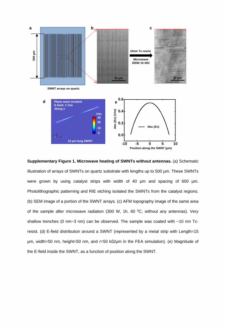
Microwave
300W 1h 60C
80
60
40
20
0
µm
806040200
µm
-4
-2
0
2
nm
80
60
40
20
0
µm
806040200
µm
-4
-2
0
2
nm
500 μ
m
SWNT arrays on quartz
30 μm 30 μm
10nm Tc-resist
a
Supplementary Figure 1. Microwave heating of SWNTs without antennas. (a) Schematic
illustration of arrays of SWNTs on quartz substrate with lengths up to 500 µm. These SWNTs
were grown by using catalyst strips with width of 40 µm and spacing of 600 µm.
Photolithographic patterning and RIE etching isolated the SWNTs from the catalyst regions.
(b) SEM image of a portion of the SWNT arrays. (c) AFM topography image of the same area
of the sample after microwave radiation (300 W, 1h, 60 0C, without any antennas). Very
shallow trenches (0 nm~3 nm) can be observed. The sample was coated with ~10 nm Tc-
resist. (d) E-field distribution around a SWNT (represented by a metal strip with Length=15
µm, width=50 nm, height=50 nm, and r=50 kΩ/μm in the FEA simulation). (e) Magnitude of
the E-field inside the SWNT, as a function of position along the SWNT.
b c
d e
30
10
0
V/m
20
Plane wave incident
E-field: 1 V/m
Along x
15 µm long SWNT -10 -5 0 5 10
0.0
0.2
0.4
0.6
Abs (Ex) Ab
s (
Ex
) (V
/m)
Position along the SWNT (μm)
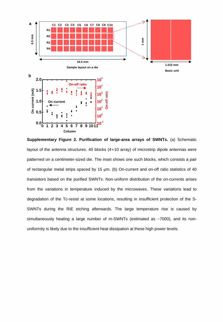
a
Sample layout on a die
16.5 mm
6.5
mm
1.015 mm
1 m
m
b
C1 C2 C3 C4 C5 C6 C7 C8 C9 C10
R1
R2
R3
R4
Basic unit
0 1 2 3 4 5 6 7 8 9 10110.0
0.5
1.0
1.5
2.0
10-1
100
101
102
103
104
105
On-off ratio
On current
On
cu
rren
t (m
A)
On
-off
rati
o
Column
Supplementary Figure 2. Purification of large-area arrays of SWNTs. (a) Schematic
layout of the antenna structures. 40 blocks (4×10 array) of microstrip dipole antennas were
patterned on a centimeter-sized die. The inset shows one such blocks, which consists a pair
of rectangular metal strips spaced by 15 µm. (b) On-current and on-off ratio statistics of 40
transistors based on the purified SWNTs. Non-uniform distribution of the on-currents arises
from the variations in temperature induced by the microwaves. These variations lead to
degradation of the Tc-resist at some locations, resulting in insufficient protection of the S-
SWNTs during the RIE etching afterwards. The large temperature rise is caused by
simultaneously heating a large number of m-SWNTs (estimated as ~7000), and its non-
uniformity is likely due to the insufficient heat dissipation at these high power levels.
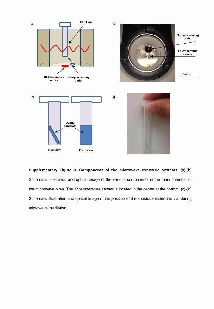
Supplementary Figure 3. Components of the microwave exposure systems. (a)-(b)
Schematic illustration and optical image of the various components in the main chamber of
the microwave oven. The IR temperature sensor is located in the center at the bottom. (c)-(d)
Schematic illustration and optical image of the position of the substrate inside the vial during
microwave irradiation.
a b
c d
Nitrogen cooling
outlet
IR temperature
sensor
Cavity
10 ml vial
IR temperature
sensor Nitrogen cooling
outlet
Side view Front view
Quartz
substrate
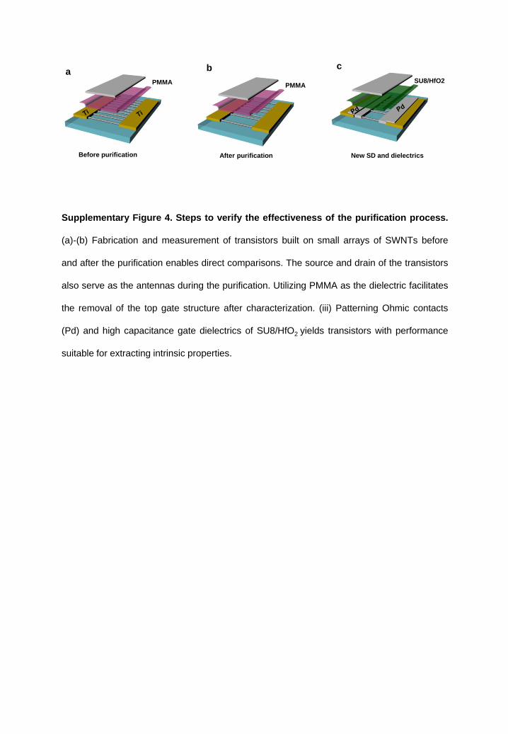
a
Before purification After purification New SD and dielectrics
PMMA SU8/HfO2 PMMA
Supplementary Figure 4. Steps to verify the effectiveness of the purification process.
(a)-(b) Fabrication and measurement of transistors built on small arrays of SWNTs before
and after the purification enables direct comparisons. The source and drain of the transistors
also serve as the antennas during the purification. Utilizing PMMA as the dielectric facilitates
the removal of the top gate structure after characterization. (iii) Patterning Ohmic contacts
(Pd) and high capacitance gate dielectrics of SU8/HfO2 yields transistors with performance
suitable for extracting intrinsic properties.
b c
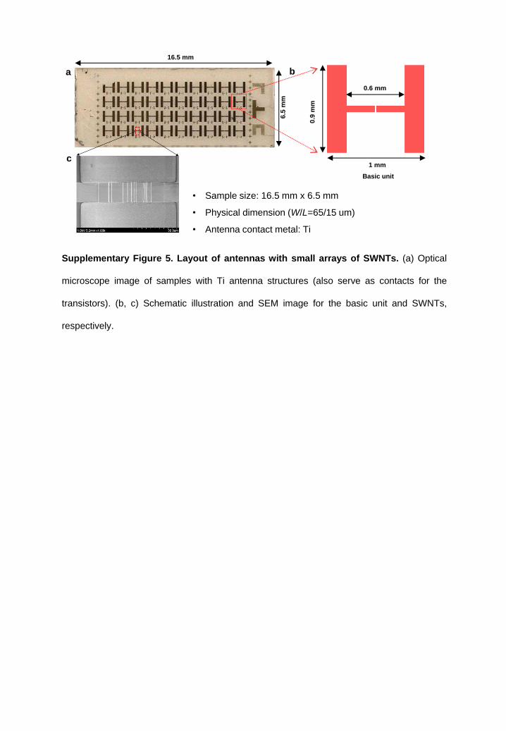
• Sample size: 16.5 mm x 6.5 mm
• Physical dimension (W/L=65/15 um)
• Antenna contact metal: Ti
Supplementary Figure 5. Layout of antennas with small arrays of SWNTs. (a) Optical
microscope image of samples with Ti antenna structures (also serve as contacts for the
transistors). (b, c) Schematic illustration and SEM image for the basic unit and SWNTs,
respectively.
a b
c
16.5 mm
6.5
mm
1 mm
0.9
mm
Basic unit
0.6 mm
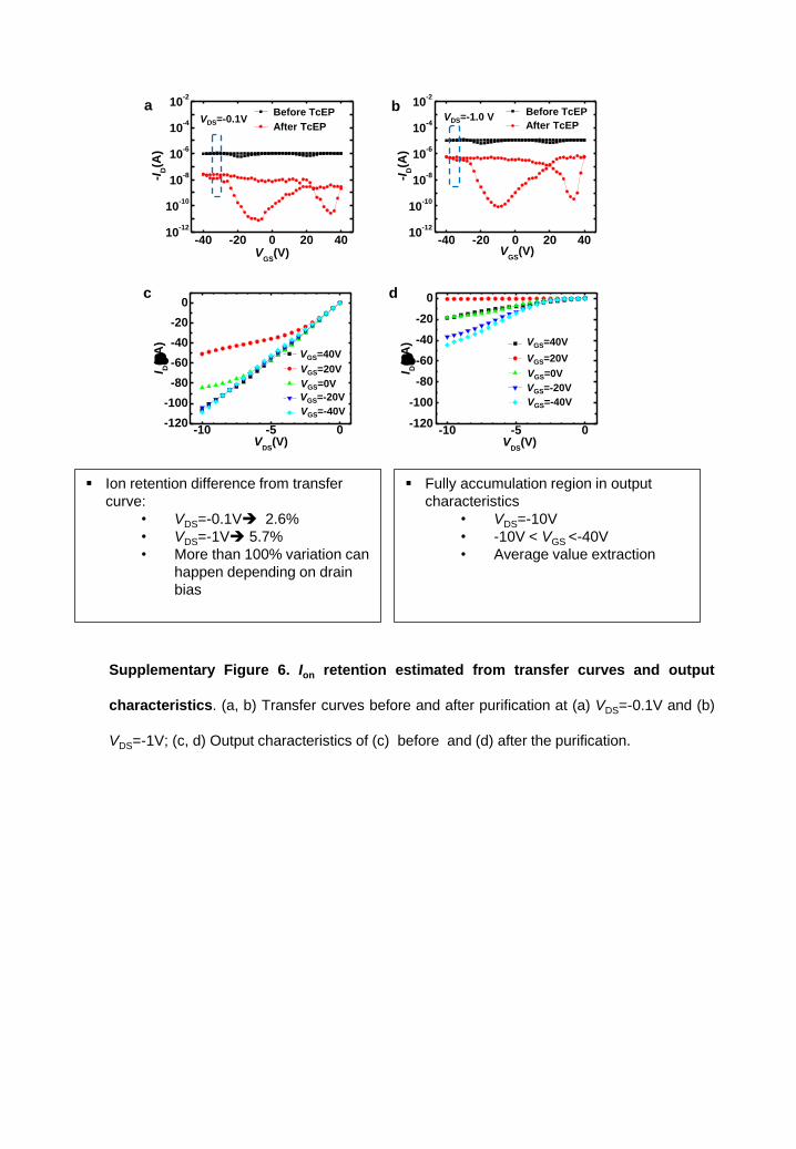
Ion retention difference from transfer
curve:
• VDS=-0.1V 2.6%
• VDS=-1V 5.7%
• More than 100% variation can
happen depending on drain
bias
Fully accumulation region in output
characteristics
• VDS=-10V
• -10V < VGS <-40V
• Average value extraction
Supplementary Figure 6. Ion retention estimated from transfer curves and output
characteristics. (a, b) Transfer curves before and after purification at (a) VDS=-0.1V and (b)
VDS=-1V; (c, d) Output characteristics of (c) before and (d) after the purification.
-40 -20 0 20 4010
-12
10-10
10-8
10-6
10-4
10-2
-ID(A
)
VGS
(V)
VDS=-0.1V
Before TcEP
After TcEP
-40 -20 0 20 4010
-12
10-10
10-8
10-6
10-4
10-2
-ID(A
)
VGS
(V)
VDS=-1.0 V Before TcEP
After TcEP
-10 -5 0-120
-100
-80
-60
-40
-20
0
I D(
A)
VDS
(V)
VGS=40V
VGS=20V
VGS=0V
VGS=-20V
VGS=-40V
-10 -5 0-120
-100
-80
-60
-40
-20
0
I D(
A)
VDS
(V)
VGS=40V
VGS=20V
VGS=0V
VGS=-20V
VGS=-40V
a b
c d
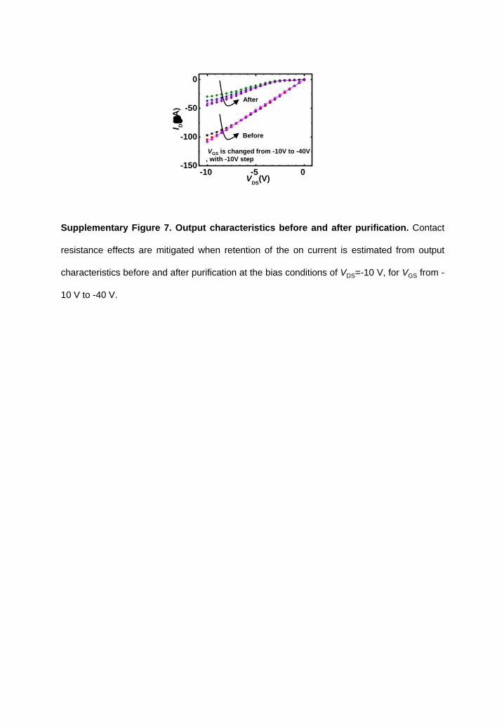
-10 -5 0-150
-100
-50
0
I D(
A)
VDS
(V)
After
VGS is changed from -10V to -40V
, with -10V step
Before
Supplementary Figure 7. Output characteristics before and after purification. Contact
resistance effects are mitigated when retention of the on current is estimated from output
characteristics before and after purification at the bias conditions of VDS=-10 V, for VGS from -
10 V to -40 V.
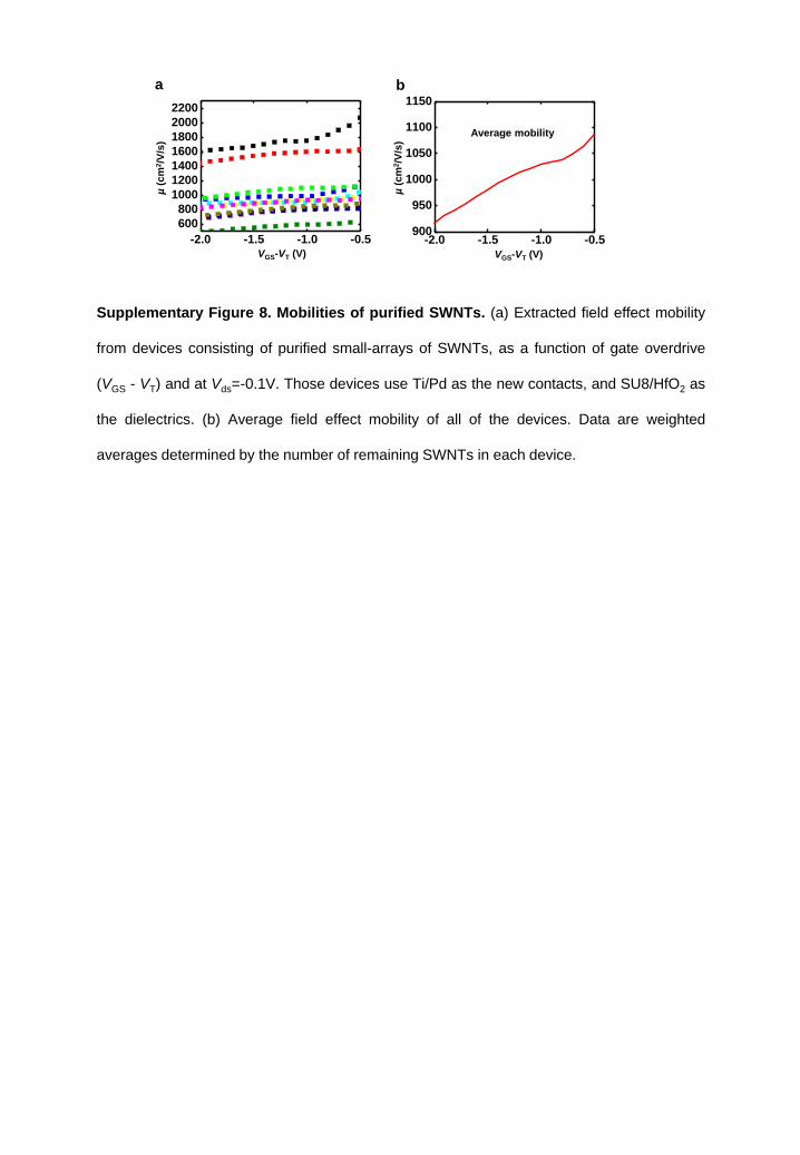
µ (
cm
2/V
/s)
VGS-VT (V)
a
-2.0 -1.5 -1.0 -0.5
600
800
1000
1200
1400
1600
1800
2000
2200
-2.0 -1.5 -1.0 -0.5900
950
1000
1050
1100
1150
µ
(c
m2/V
/s)
VGS-VT (V)
b
Average mobility
Supplementary Figure 8. Mobilities of purified SWNTs. (a) Extracted field effect mobility
from devices consisting of purified small-arrays of SWNTs, as a function of gate overdrive
(VGS - VT) and at Vds=-0.1V. Those devices use Ti/Pd as the new contacts, and SU8/HfO2 as
the dielectrics. (b) Average field effect mobility of all of the devices. Data are weighted
averages determined by the number of remaining SWNTs in each device.
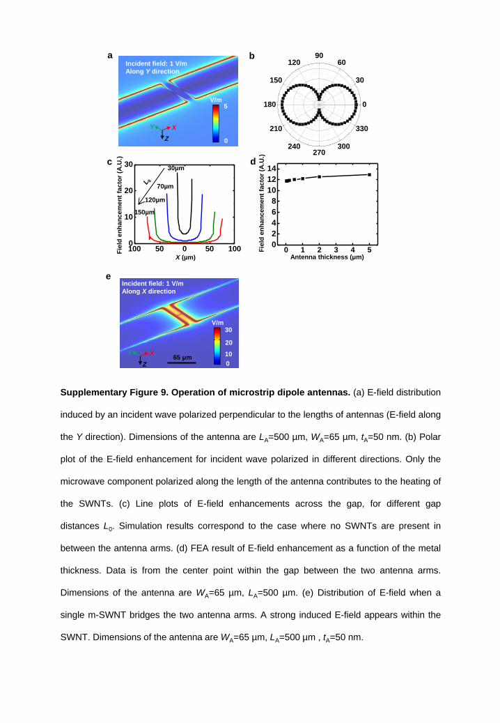
100 50 0 50 1000
10
20
30
X (µm)
30µm
70µm
120µm
150µm
Fie
ld e
nh
an
ce
me
nt
fac
tor
(A.U
.)
b a
c
0
30
6090
120
150
180
210
240270
300
330
d
Supplementary Figure 9. Operation of microstrip dipole antennas. (a) E-field distribution
induced by an incident wave polarized perpendicular to the lengths of antennas (E-field along
the Y direction). Dimensions of the antenna are LA=500 µm, WA=65 µm, tA=50 nm. (b) Polar
plot of the E-field enhancement for incident wave polarized in different directions. Only the
microwave component polarized along the length of the antenna contributes to the heating of
the SWNTs. (c) Line plots of E-field enhancements across the gap, for different gap
distances L0. Simulation results correspond to the case where no SWNTs are present in
between the antenna arms. (d) FEA result of E-field enhancement as a function of the metal
thickness. Data is from the center point within the gap between the two antenna arms.
Dimensions of the antenna are WA=65 µm, LA=500 µm. (e) Distribution of E-field when a
single m-SWNT bridges the two antenna arms. A strong induced E-field appears within the
SWNT. Dimensions of the antenna are WA=65 µm, LA=500 µm , tA=50 nm.
0 1 2 3 4 50
2
4
6
8
10
12
14
Fie
ld e
nh
an
ce
me
nt
fac
tor
(A.U
.)
Antenna thickness (μm)
0
V/m 5
Incident field: 1 V/m
Along Y direction
X
Z
Y
Incident field: 1 V/m
Along X direction
30
10
0
V/m
20
X
Z
Y 65 μm
e
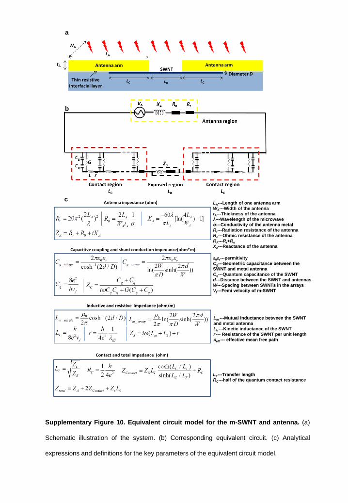
b
a
Supplementary Figure 10. Equivalent circuit model for the m-SWNT and antenna. (a)
Schematic illustration of the system. (b) Corresponding equivalent circuit. (c) Analytical
expressions and definitions for the key parameters of the equivalent circuit model.
c LA---Length of one antenna arm
WA---Width of the antenna
tA---Thickness of the antenna
λ---Wavelength of the microwave
σ---Conductivity of the antenna metal
Rr---Radiation resistance of the antenna
Ro---Ohmic resistance of the antenna
RA---Rr+Ro
XA---Reactance of the antenna
ε0εr---permitivity
Cg---Geometric capacitance between the
SWNT and metal antenna
Cq---Quantum capacitance of the SWNT
d---Distance between the SWNT and antennas
W---Spacing between SWNTs in the arrays
Vf---Femi velocity of m-SWNT
Lm ---Mutual inductance between the SWNT
and metal antenna
Lk ---Kinetic inductance of the SWNT
r --- Resistance of the SWNT per unit length
λeff --- effective mean free path
LT---Transfer length
RC---half of the quantum contact resistance
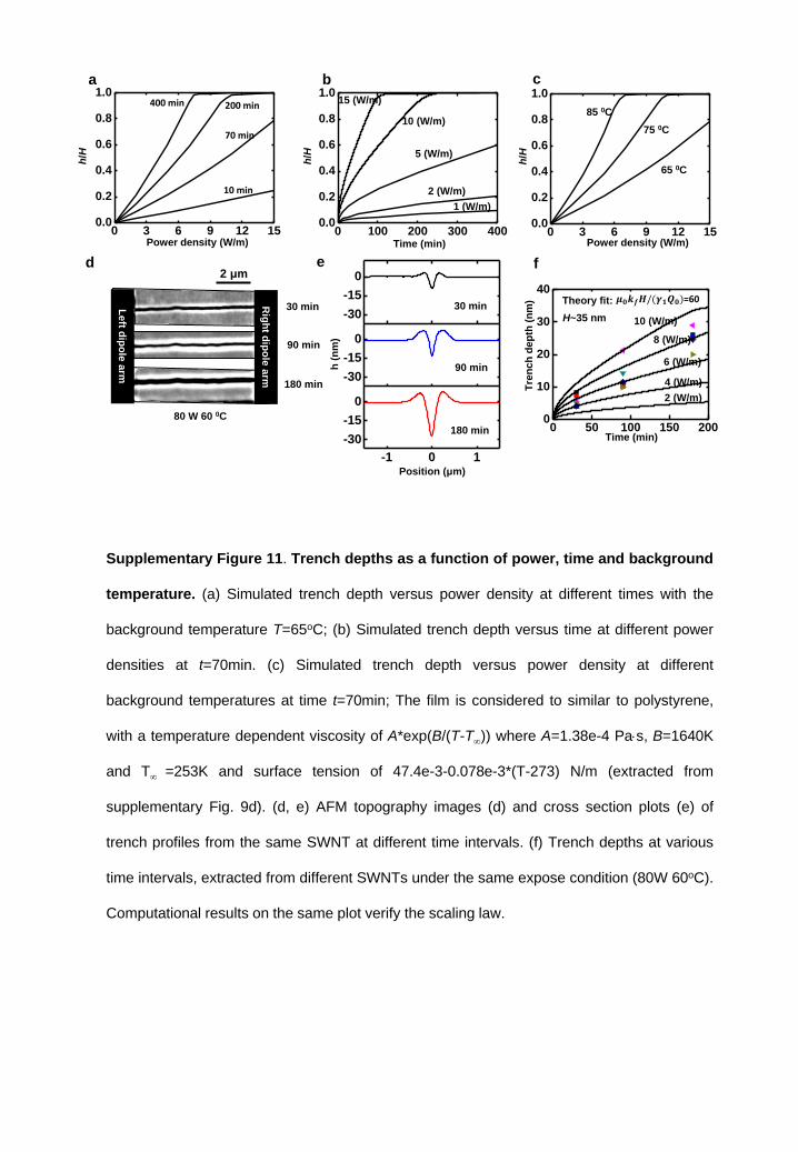
0 50 100 150 2000
10
20
30
40
0 3 6 9 12 150.0
0.2
0.4
0.6
0.8
1.0
0 100 200 300 4000.0
0.2
0.4
0.6
0.8
1.0
0 3 6 9 12 150.0
0.2
0.4
0.6
0.8
1.0
-1 0 1
-30
-15
0
-30
-15
0
-30
-15
0
a h
/H
Power density (W/m)
400 min 200 min
70 min
10 min
15 (W/m)
10 (W/m)
5 (W/m)
2 (W/m)
1 (W/m)
h/H
b c
180 min
90 min
30 min
80 W 60 0C
2 μm
Le
ft dip
ole
arm
Rig
ht d
ipo
le a
rm
d e f
Position (μm)
h (
nm
)
30 min
90 min
180 min Time (min)
Tre
nc
h d
ep
th (
nm
) Theory fit: 𝝁𝟎𝒌𝒇𝑯/(𝜸𝟏𝑸𝟎)=60
Supplementary Figure 11. Trench depths as a function of power, time and background
temperature. (a) Simulated trench depth versus power density at different times with the
background temperature T=65oC; (b) Simulated trench depth versus time at different power
densities at t=70min. (c) Simulated trench depth versus power density at different
background temperatures at time t=70min; The film is considered to similar to polystyrene,
with a temperature dependent viscosity of A*exp(B/(T-T)) where A=1.38e-4 Pas, B=1640K
and T =253K and surface tension of 47.4e-3-0.078e-3*(T-273) N/m (extracted from
supplementary Fig. 9d). (d, e) AFM topography images (d) and cross section plots (e) of
trench profiles from the same SWNT at different time intervals. (f) Trench depths at various
time intervals, extracted from different SWNTs under the same expose condition (80W 60oC).
Computational results on the same plot verify the scaling law.
Time (min)
h/H
Power density (W/m)
65 0C
75 0C
85 0C
H~35 nm
2 (W/m)
4 (W/m)
6 (W/m)
8 (W/m)
10 (W/m)
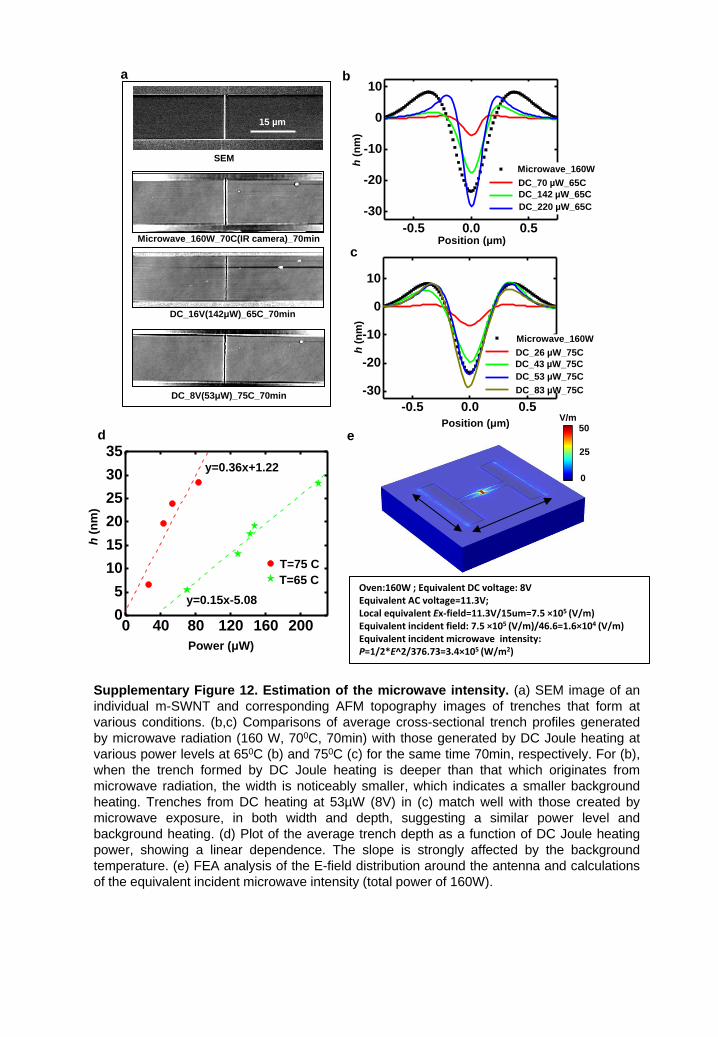
-0.5 0.0 0.5
-30
-20
-10
0
10
0 40 80 120 160 2000
5
10
15
20
25
30
35
15
10
5
0
µm
6050403020100
µm
-4-2024
nm
25
20
15
10
5
0
µm
706050403020100
µm
-4
-2
0
2
4
nm
-0.5 0.0 0.5
-30
-20
-10
0
10
Microwave_160W
DC_70 µW_65C
DC_142 µW_65C
DC_220 µW_65C
Position (μm)
h (
nm
) h
(n
m)
Position (μm)
Microwave_160W
DC_26 µW_75C
DC_43 µW_75C
DC_53 µW_75C
DC_83 µW_75C
a b
c
SEM
15 µm
Microwave_160W_70C(IR camera)_70min
DC_16V(142μW)_65C_70min
DC_8V(53μW)_75C_70min
d
Power (μW)
h (
nm
)
T=75 C
T=65 C
y=0.15x-5.08
y=0.36x+1.22
25
20
15
10
5
0
µm
706050403020100
µm
-4
-2
0
2
4
nm
e 50
0
V/m
25
Supplementary Figure 12. Estimation of the microwave intensity. (a) SEM image of an
individual m-SWNT and corresponding AFM topography images of trenches that form at
various conditions. (b,c) Comparisons of average cross-sectional trench profiles generated
by microwave radiation (160 W, 700C, 70min) with those generated by DC Joule heating at
various power levels at 650C (b) and 750C (c) for the same time 70min, respectively. For (b),
when the trench formed by DC Joule heating is deeper than that which originates from
microwave radiation, the width is noticeably smaller, which indicates a smaller background
heating. Trenches from DC heating at 53µW (8V) in (c) match well with those created by
microwave exposure, in both width and depth, suggesting a similar power level and
background heating. (d) Plot of the average trench depth as a function of DC Joule heating
power, showing a linear dependence. The slope is strongly affected by the background
temperature. (e) FEA analysis of the E-field distribution around the antenna and calculations
of the equivalent incident microwave intensity (total power of 160W).
Oven:160W ; Equivalent DC voltage: 8V Equivalent AC voltage=11.3V; Local equivalent Ex-field=11.3V/15um=7.5 ×105 (V/m) Equivalent incident field: 7.5 ×10⁵ (V/m)/46.6=1.6×104 (V/m) Equivalent incident microwave intensity: P=1/2*E^2/376.73=3.4×105 (W/m2)
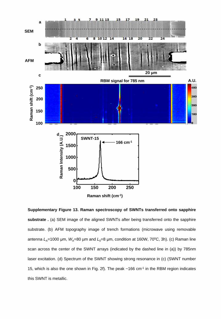
Supplementary Figure 13. Raman spectroscopy of SWNTs transferred onto sapphire
substrate . (a) SEM image of the aligned SWNTs after being transferred onto the sapphire
substrate. (b) AFM topography image of trench formations (microwave using removable
antenna LA=1000 μm, WA=80 µm and L0=8 μm, condition at 160W, 700C, 3h). (c) Raman line
scan across the center of the SWNT arrays (indicated by the dashed line in (a)) by 785nm
laser excitation. (d) Spectrum of the SWNT showing strong resonance in (c) (SWNT number
15, which is also the one shown in Fig. 2f). The peak ~166 cm-1 in the RBM region indicates
this SWNT is metallic.
a
b
c
d
80
60
40
20
0
µm
806040200
µm
-8
-6
-4
-2
0
nm
SEM
AFM
20 μm
100 150 200 250
0
500
1000
1500
2000
Raman shift (cm-1)
Ra
ma
n In
ten
sit
y (
A.U
.)
SWNT-15 166 cm-1
A.U. RBM signal for 785 nm
100
250
200
150
Ra
ma
n s
hif
t (c
m-1
)
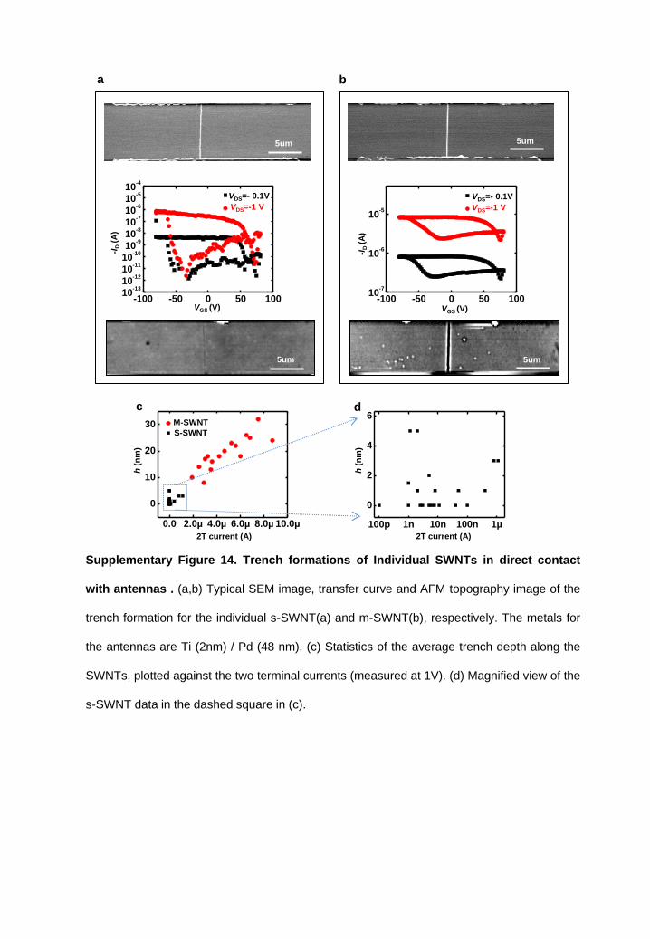
0.0 2.0µ 4.0µ 6.0µ 8.0µ 10.0µ
0
10
20
30
a b
5um 5um
16
14
12
10
8
6
4
2
0
µm
403020100
µm
-4
-2
0
2
4
nm
5um
12
10
8
6
4
2
0
µm
403020100
µm
-4
-2
0
2
4
nm
c
-100 -50 0 50 10010
-1310
-1210
-1110
-1010
-910
-810
-710
-610
-510
-4
-100 -50 0 50 10010
-7
10-6
10-5
5um
VGS (V)
VDS=- 0.1V
VDS=-1 V
-ID
(A
)
VGS (V)
VDS=- 0.1V
VDS=-1 V
-ID
(A
)
100p 1n 10n 100n 1µ
0
2
4
6
2T current (A)
h (
nm
)
2T current (A)
h (
nm
)
d
M-SWNT
S-SWNT
Supplementary Figure 14. Trench formations of Individual SWNTs in direct contact
with antennas . (a,b) Typical SEM image, transfer curve and AFM topography image of the
trench formation for the individual s-SWNT(a) and m-SWNT(b), respectively. The metals for
the antennas are Ti (2nm) / Pd (48 nm). (c) Statistics of the average trench depth along the
SWNTs, plotted against the two terminal currents (measured at 1V). (d) Magnified view of the
s-SWNT data in the dashed square in (c).
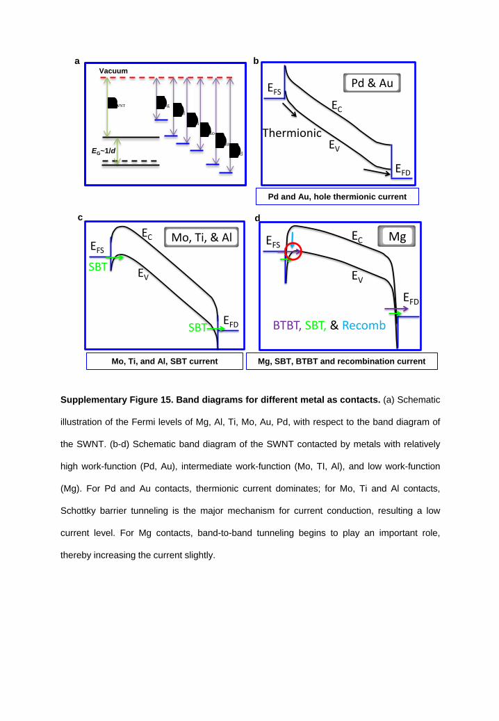
a Vacuum
SWNT Mg
EG~1/d
Al
Ti
Mo
Au
Pd
Pd and Au, hole thermionic current
EFD
EFS
EC
EV
Pd & Au
Thermionic
b
c d
Mo, Ti, and Al, SBT current
EFS
EFD
SBT
SBT
EC
EV
Mo, Ti, & Al
Mg, SBT, BTBT and recombination current
BTBT, SBT, & Recomb
EC
EV
EFS
EFD
Mg
Supplementary Figure 15. Band diagrams for different metal as contacts. (a) Schematic
illustration of the Fermi levels of Mg, Al, Ti, Mo, Au, Pd, with respect to the band diagram of
the SWNT. (b-d) Schematic band diagram of the SWNT contacted by metals with relatively
high work-function (Pd, Au), intermediate work-function (Mo, TI, Al), and low work-function
(Mg). For Pd and Au contacts, thermionic current dominates; for Mo, Ti and Al contacts,
Schottky barrier tunneling is the major mechanism for current conduction, resulting a low
current level. For Mg contacts, band-to-band tunneling begins to play an important role,
thereby increasing the current slightly.
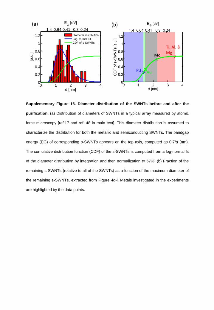
1.4 0.64 0.41 0.3 0.24
EG
[eV]
0 1 2 3 40
0.2
0.4
0.6
0.8
1
1.2
d [nm]
[a.u
.]
Diameter distribution
Log-normal Fit
CDF of s-SWNTs
Pd Au
Mo
Ti, Al, & Mg
(a) (b)
Supplementary Figure 16. Diameter distribution of the SWNTs before and after the
purification. (a) Distribution of diameters of SWNTs in a typical array measured by atomic
force microscopy [ref.17 and ref. 48 in main text]. This diameter distribution is assumed to
characterize the distribution for both the metallic and semiconducting SWNTs. The bandgap
energy (EG) of corresponding s-SWNTs appears on the top axis, computed as 0.7/d (nm).
The cumulative distribution function (CDF) of the s-SWNTs is computed from a log-normal fit
of the diameter distribution by integration and then normalization to 67%. (b) Fraction of the
remaining s-SWNTs (relative to all of the SWNTs) as a function of the maximum diameter of
the remaining s-SWNTs, extracted from Figure 4d-i. Metals investigated in the experiments
are highlighted by the data points.
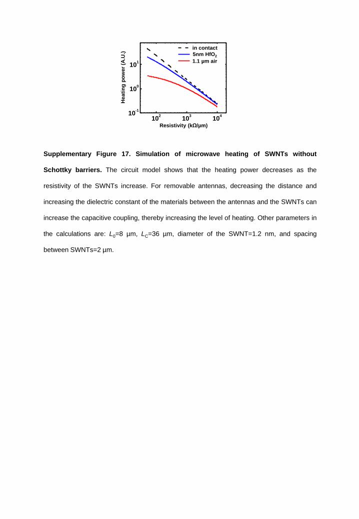
102
103
10410
-1
100
101
Heati
ng
po
wer
(A.U
.)
Resistivity (kΩ/µm)
in contact
5nm HfO2
1.1 µm air
Supplementary Figure 17. Simulation of microwave heating of SWNTs without
Schottky barriers. The circuit model shows that the heating power decreases as the
resistivity of the SWNTs increase. For removable antennas, decreasing the distance and
increasing the dielectric constant of the materials between the antennas and the SWNTs can
increase the capacitive coupling, thereby increasing the level of heating. Other parameters in
the calculations are: L0=8 µm, LC=36 µm, diameter of the SWNT=1.2 nm, and spacing
between SWNTs=2 µm.
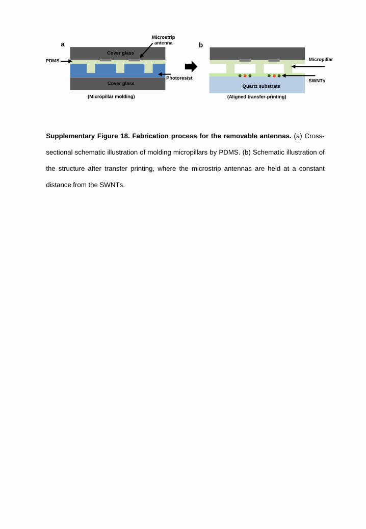
Supplementary Figure 18. Fabrication process for the removable antennas. (a) Cross-
sectional schematic illustration of molding micropillars by PDMS. (b) Schematic illustration of
the structure after transfer printing, where the microstrip antennas are held at a constant
distance from the SWNTs.
(Micropillar molding)
Cover glass
PDMS
a Microstrip
antenna
Cover glass Photoresist
b
SWNTs Quartz substrate
(Aligned transfer-printing)
Micropillar
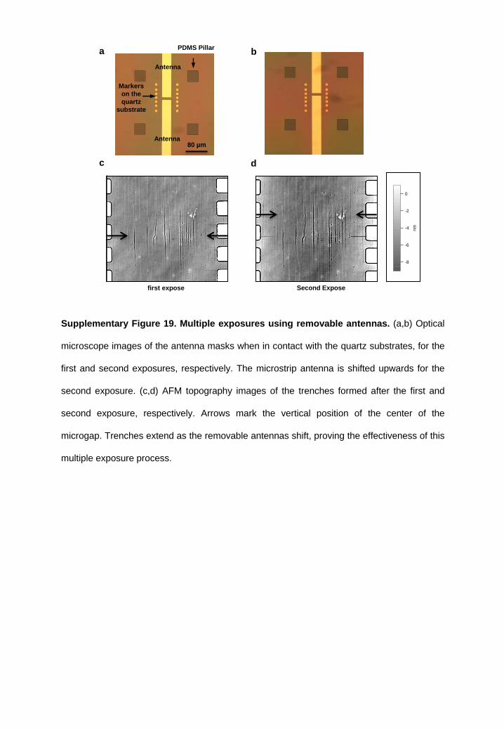
80
60
40
20
0
µm
806040200
µm
-8
-6
-4
-2
0
nm
first expose
80
60
40
20
0
µm
806040200
µm
-8
-6
-4
-2
0
nm
Second Expose
a b
c d
80 µm
80
60
40
20
0
µm
806040200
µm
-8
-6
-4
-2
0
nm
Supplementary Figure 19. Multiple exposures using removable antennas. (a,b) Optical
microscope images of the antenna masks when in contact with the quartz substrates, for the
first and second exposures, respectively. The microstrip antenna is shifted upwards for the
second exposure. (c,d) AFM topography images of the trenches formed after the first and
second exposure, respectively. Arrows mark the vertical position of the center of the
microgap. Trenches extend as the removable antennas shift, proving the effectiveness of this
multiple exposure process.
Markers
on the
quartz
substrate
Antenna
PDMS Pillar
Antenna
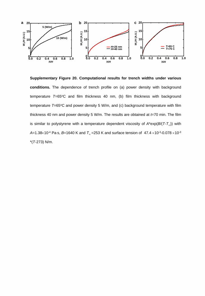
0.0 0.2 0.4 0.6 0.8 1.00
5
10
15
20
0.0 0.2 0.4 0.6 0.8 1.00
5
10
15
20
0.0 0.2 0.4 0.6 0.8 1.00
5
10
15
20
WT/H
(A
.U.)
h/H
5 (W/m)
10 (W/m)
H=25 nm H=40 nm
WT/H
(A
.U.)
h/H
b
WT/H
(A
.U.)
h/H
T=65 C T=75 C
a c
Supplementary Figure 20. Computational results for trench widths under various
conditions. The dependence of trench profile on (a) power density with background
temperature T=65oC and film thickness 40 nm, (b) film thickness with background
temperature T=65oC and power density 5 W/m, and (c) background temperature with film
thickness 40 nm and power density 5 W/m. The results are obtained at t=70 min. The film
is similar to polystyrene with a temperature dependent viscosity of A*exp(B/(T-T)) with
A=1.3810-4 Pas, B=1640 K and T =253 K and surface tension of 47.4 10-3-0.078 10-3
*(T-273) N/m.
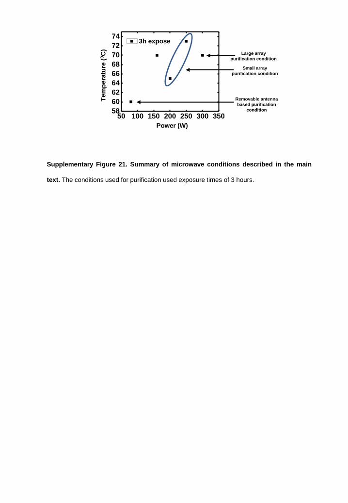
Supplementary Figure 21. Summary of microwave conditions described in the main
text. The conditions used for purification used exposure times of 3 hours.
50 100 150 200 250 300 35058
60
62
64
66
68
70
72
74
Power (W)
Te
mp
era
ture
(0C
)
3h expose
Large array
purification condition
Small array
purification condition
Removable antenna
based purification
condition

VGS=-10V VGS=-20V VGS=-30V VGS=-40V
Before TcEP -9.68E-05 -1.04E-04 -1.07E-04 -1.09E-04
After After TcEP -2.94E-05 -3.68E-05 -4.15E-05 -4.47E-05
Ratio 3.03E-01 3.53E-01 3.86E-01 4.11E-01
Average Ratio 0.36 STD 0.05
Supplementary Table 1. Ion retentions based on the output currents at VDS=-10 V. Data
in this table is extracted from Supplementary Fig. 7. The average value is calculated from 4
data points, including VGS=-10 V, VGS=-20 V, VGS=-30 V and VGS=-40 V.
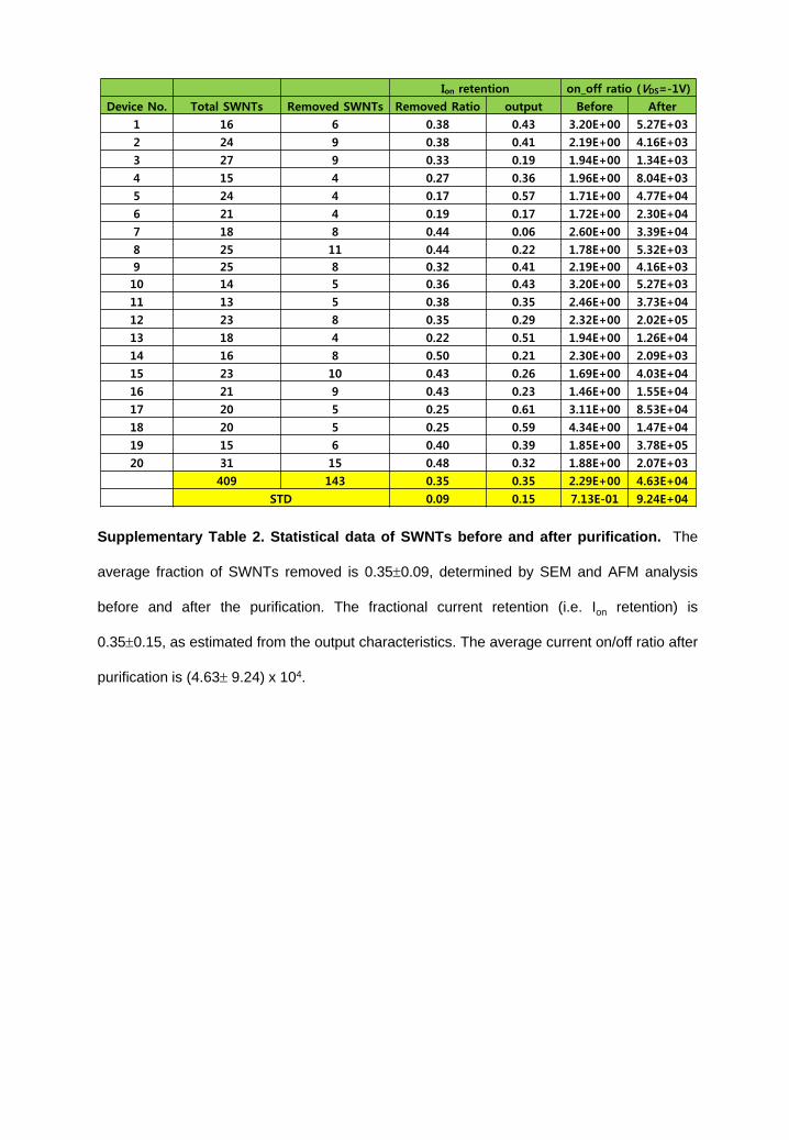
Ion retention on_off ratio (VDS=-1V)
Device No. Total SWNTs Removed SWNTs Removed Ratio output Before After
1 16 6 0.38 0.43 3.20E+00 5.27E+03
2 24 9 0.38 0.41 2.19E+00 4.16E+03
3 27 9 0.33 0.19 1.94E+00 1.34E+03
4 15 4 0.27 0.36 1.96E+00 8.04E+03
5 24 4 0.17 0.57 1.71E+00 4.77E+04
6 21 4 0.19 0.17 1.72E+00 2.30E+04
7 18 8 0.44 0.06 2.60E+00 3.39E+04
8 25 11 0.44 0.22 1.78E+00 5.32E+03
9 25 8 0.32 0.41 2.19E+00 4.16E+03
10 14 5 0.36 0.43 3.20E+00 5.27E+03
11 13 5 0.38 0.35 2.46E+00 3.73E+04
12 23 8 0.35 0.29 2.32E+00 2.02E+05
13 18 4 0.22 0.51 1.94E+00 1.26E+04
14 16 8 0.50 0.21 2.30E+00 2.09E+03
15 23 10 0.43 0.26 1.69E+00 4.03E+04
16 21 9 0.43 0.23 1.46E+00 1.55E+04
17 20 5 0.25 0.61 3.11E+00 8.53E+04
18 20 5 0.25 0.59 4.34E+00 1.47E+04
19 15 6 0.40 0.39 1.85E+00 3.78E+05
20 31 15 0.48 0.32 1.88E+00 2.07E+03
409 143 0.35 0.35 2.29E+00 4.63E+04
STD 0.09 0.15 7.13E-01 9.24E+04
Supplementary Table 2. Statistical data of SWNTs before and after purification. The
average fraction of SWNTs removed is 0.350.09, determined by SEM and AFM analysis
before and after the purification. The fractional current retention (i.e. Ion retention) is
0.350.15, as estimated from the output characteristics. The average current on/off ratio after
purification is (4.63 9.24) x 104.
Supplementary Note 1: Multi-cycles of Tc-resist deposition and microwave radiation
Three cycles of Tc-resist deposition and microwave irradiation ensure the full protection of the
unexposed s-SWNTs, even when processing conditions of the etching tools vary slightly. Details
of the processes are: (1) deposition of Tc-resist (~35 nm), and microwave irradiation at 250 W,
73 0C, 3 h; (2) deposition of Tc-resist (~20 nm), and microwave irradiation at 200 W, 65
0C, 3 h;
(3) deposition of Tc-resist (~20 nm), and microwave irradiation at 200 W, 65 0C, 3 h. This
multiple layer scheme enhances the etch resistance by increasing the thickness of the Tc-resist.
Furthermore, the multiple depositions also help to eliminate the effects of pinholes that form in
single layers.
Supplementary Note 2: Mobility extraction
The characterization of average field effect mobility () per SWNT within a device at
different VGS involves modeling of ID-VGS characteristics, measured at VGS >> VT and at small
VDS ~ 0.1V, using the following expression:
D G GS T DSI C W L V V V (1)
Here, W = 50 μm is the width and L = 5 μm is the length of the transistor. Threshold voltage (VT)
for equation (1) is calculated from the x-axis intercept of the slope on ID-VGS curve, drawn at
maximum transconductance (gm,max ≡ max of ∂ID/∂VGS) point. Gate to channel capacitance (CG)
is calculated by considering the effect of SWNT density (DSWNT = 1/λ0, where is the average
spacing between two SWNTs) and quantum capacitance (CQ)1:
1 1
0G ox QC C C (2)
In equation (2), oxide capacitance (Cox) is defined using –
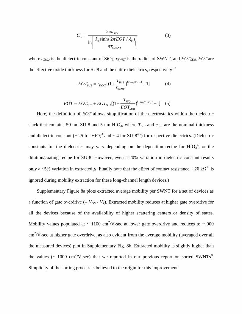
2
0 0
2
sinh 2 /ln
SiO
ox
SWCNT
CEOT
r
(3)
where εSiO2 is the dielectric constant of SiO2, rSWNT is the radius of SWNT, and EOTSU8, EOT are
the effective oxide thickness for SU8 and the entire dielectrics, respectively: 2
82( / )8
8 [(1 ) 1]SiO SUSUSU SWNT
SWNT
TEOT r
r
(4)
2 2 2( / )
8 8
8
[(1 ) 1]SiO HfOHfO
SU SU
SU
TEOT EOT EOT
EOT
(5)
Here, the definition of EOT allows simplification of the electrostatics within the dielectric
stack that contains 50 nm SU-8 and 5 nm HfO2, where T(…) and ε(…) are the nominal thickness
and dielectric constant (~ 25 for HfO23 and ~ 4 for SU-8
4,5) for respective dielectrics. (Dielectric
constants for the dielectrics may vary depending on the deposition recipe for HfO26, or the
dilution/coating recipe for SU-8. However, even a 20% variation in dielectric constant results
only a ~5% variation in extracted . Finally note that the effect of contact resistance ~ 28 kΩ7 is
ignored during mobility extraction for these long-channel length devices.)
Supplementary Figure 8a plots extracted average mobility per SWNT for a set of devices as
a function of gate overdrive (≡ VGS - VT). Extracted mobility reduces at higher gate overdrive for
all the devices because of the availability of higher scattering centers or density of states.
Mobility values populated at ~ 1100 cm2/V-sec at lower gate overdrive and reduces to ~ 900
cm2/V-sec at higher gate overdrive, as also evident from the average mobility (averaged over all
the measured devices) plot in Supplementary Fig. 8b. Extracted mobility is slightly higher than
the values (~ 1000 cm2/V-sec) that we reported in our previous report on sorted SWNTs
8.
Simplicity of the sorting process is believed to the origin for this improvement.
Supplementary Note 3: Discussion of equivalent circuit model
Equivalent circuit in Fig. 2c and Supplementary Fig. 10a-c show three major regions, namely the
antenna region, the contact region, and the load region.
For the antenna region, the equivalent voltage is inferred from FEA simulation and associated
experiments (Supplementary Fig.12). The resistance (~120 Ω) of the antenna is negligible
compared to the contribution of capacitance to the impedance (~-4×10³
Ω, or ~-1×10⁴
Ω if
assuming surroundings of antennas are all air), for the typical antenna structure LA=1000 µm,
WA=65 µm, tA=50 nm.
Regarding the contact region, we assume that the shunt conductance G is infinite (perfect
contact) if the SWNTs are in direct contact with the antennas. Without direct contact, G is set to
be 0. Both the mutual inductance and kinetic inductance are small for the SWNTs, resulting in
negligible impedance (~60 Ω/µm). Therefore, the resistances of the SWNTs dominate the total
impedance. The current transfers from the antenna to the SWNTs within a characteristic length
(LT), take the form sinh(x/LT) /sinh(LC/LT) (where the end of the antenna is at the origin of the x-
axis).
For the load region, only the resistance and inductance are considered. Ignoring the capacitive
coupling between the center segments of the SWNT to the surroundings simplifies the
calculation.
Supplementary Note 4: Transfer printing of SWNTs for Raman spectroscopy
Transfer printing of the aligned arrays of SWNTs from the quartz substrate to an ɑ-plane
sapphire substrate facilitates the Raman spectroscopy (to determine the type of the SWNTs
without electrical contacts), due to absence of peaks (below ~378 cm-1
) associated with the
sapphire in the radial breathing mode (RBM) region of SWNTs (Supplementary Fig. 13). To
perform the transfer, a thin layer of poly(vinyl alcohol) (PVA, Sigma-Aldrich, dissolved in water
~ 5% as percentage by weight) was first drop-casted on the quartz substrate. Baking the substrate
at 60 0C for 10 min eliminated the solvent. Thermal tape allowed retrieval of the PVA film (with
the SWNTs) and release onto the a-plane sapphire substrate at 110 0C. Immersion of the
sapphire/SWNTs/PVA substrate in hot water (700C) for 3 h washed away the PVA film. Raman
spectroscopy was carried out on a Raman confocal imaging microscope (Horiba LabRAM HR
3D, equipped with four lasers, 532nm, 633nm, 785nm and 830nm) under ambient conditions.
Supplementary Note 5: Model for charge transport
Simulation of average current and power dissipation of s-SWNT involves a self-consistent
solution of spatially-resolved 3D electrostatics potential and charge density distributions. The 3D
electrostatics accounts for the complete device geometry: the SWNTs on the quartz substrate are
terminated by source (S) and drain (D) contacts, and covered by insulating material Tc-resist. To
calculate the potential from Eq. (3) of main text, we use the Dirichlet boundary conditions at the
source and the drain metallic contacts and assign fixed potentials, namely, ФS and VDS - ФD, to
the respective contacts. Here, ФS and ФD are the work functions of the source and drain,
respectively, and VDS is the applied drain bias. The Neumann boundary conditions on the
exposed surfaces of the quartz substrate and Tc-resist9 ensure that the normal component of the
electric field is zero.
The solution of the Eq. 3 in the main text depends on the charge density - - ;aq p n N
the charge density along the channel is obtained by calculating carrier densities (electron (n) and
hole (p)) through drift-diffusion equations (Eqs. (4)-(7) of main text), and through independent
determination of the ionized impurity ( aN ) concentrations.
We follow two different ways to calculate carrier concentrations depending on biasing
arrangement. First, at VDS = 0, the device is in equilibrium, therefore, the Fermi level is flat
throughout the device and is aligned with source and drain. Electron and hole concentrations are
computed as,
1/2 C n pn p N (6)
where, effective density of states are
0
8
4 3
G B BC
G G
E k T k TN
a E E
,10
1/2 is the Fermi-Dirac
integral of order one-half,
Fn Cn
B
E E
k T
,
V Fp
p
B
E E
k T
, α = 1-2 is the zone degeneracy
coefficient, the graphene lattice constant is a = 0.246 nm, γ0 ~ 3 eV is the π-bond energy, ( )Fn pE
is quasi-Fermi energy for electrons (holes), and EC(V) is the conduction (valence) band energies.
Second, when VDS ≠ 0, Fermi-level are no longer constant along the channel of the s-SWNT,
therefore, carrier concentrations must now be calculated by solving continuity equation. The
electron and hole boundary currents ( snI andspI ) of the continuity equation have the following
expressions:
, ,; sn sn equi sp sp equiS D S D
I qv n n I qv p p (7)
where, 1/2 , ,,equi C n S n Dn N or , 1/2 , ,,equi C p S p Dp N or , ( )sn spv is the surface
recombination velocity of electron (hole), equal to half of the thermal velocity11
, ,
( )S D
n p is the
concentration of electron (hole) at the interfaces of Source/SWNT and Drain/SWNT and is
obtained by solving Eqs. (4)-(7) of the main text. Note that the diffusion coefficients (Dn(p)) used
in Eq. (7) of the main text appropriately account for the Fermi-Dirac distribution,
1/2 1/2,
B
n p FE n p n p n p
k TD
q
(8)
Ionized impurity concentration, aN , represents the influence of negatively charged interface
defect12
on the electrostatics of s-SWNT through the relation
1 4exp 0.045 /a a V Fp BN N E E k T
(9)
where, Na = 4.4x10¹⁹
cm-3
is the uniform concentration of the impurity throughout the s-SWNT9.
Supplementary References:
1 Cao, Q. et al. Gate capacitance coupling of singled-walled carbon nanotube thin-film transistors. Appl. Phys. Lett. 90 (2007).
2 Tienda-Luna, I. M., Ruiz, F. J. G., Donetti, L., Godoy, A. & Gamiz, F. Modeling the equivalent oxide thickness of Surrounding Gate SOI devices with high-kappa insulators. Solid State Electron. 52, 1854-1860 (2008).
3 Wilk, G. D., Wallace, R. M. & Anthony, J. M. High-kappa gate dielectrics: Current status and materials properties considerations. J. Appl. Phys. 89, 5243-5275 (2001).
4 Thorpe, J. R., Steenson, D. P. & Miles, R. E. High frequency transmission line using micromachined polymer dielectric. Electron. Lett. 34, 1237-1238 (1998).
5 Processing Guidelines for SU-8 2000.5. <http://www.microchem.com> (2014). 6 Hsu, C. T., Su, Y. K. & Yokoyama, M. High Dielectric-Constant of Rf-Sputtered Hfo2 Thin-Films.
Jpn. J. Appl. Phys. 1 31, 2501-2504 (1992). 7 Zhou, X. J., Park, J. Y., Huang, S. M., Liu, J. & McEuen, P. L. Band structure, phonon scattering,
and the performance limit of single-walled carbon nanotube transistors. Phys. Rev. Lett. 95 (2005).
8 Jin, S. H. et al. Using nanoscale thermocapillary flows to create arrays of purely semiconducting single-walled carbon nanotubes. Nat. Nanotech. 8, 347-355 (2013).
9 Xie, X. et al. Electroluminescence in Aligned Arrays of Single-Wall Carbon Nanotubes with Asymmetric Contacts. Acs Nano 6, 7981-7988 (2012).
10 Akinwande, D., Nishi, Y. & Wong, H. S. P. An analytical derivation of the density of states, effective mass, and carrier density for achiral carbon nanotubes. Ieee T. Electron. Dev. 55, 289-297 (2008).
11 Traversa, F. L. et al. A Generalized Drift-Diffusion Model for Rectifying Schottky Contact Simulation. Ieee T. Electron. Dev. 57, 1539-1547 (2010).
12 Kim, W. et al. Hysteresis caused by water molecules in carbon nanotube field-effect transistors. Nano Lett. 3, 193-198 (2003).