Master and PhD Thesis Projects 2017 - Spintec
30
Date : 29 Sep 2016 [p.1] Master and PhD Thesis Projects 2017 SPINTRONIQUE et TECHNOLOGIE des COMPOSANTS http://www.spintec.fr
Transcript of Master and PhD Thesis Projects 2017 - Spintec
Date : 29 Sep 2016 [p.1]
Master and PhD Thesis Projects 2017
SPINTRONIQUE et TECHNOLOGIE des COMPOSANTS
http://www.spintec.fr
Date : 29 Sep 2016 [p.2]
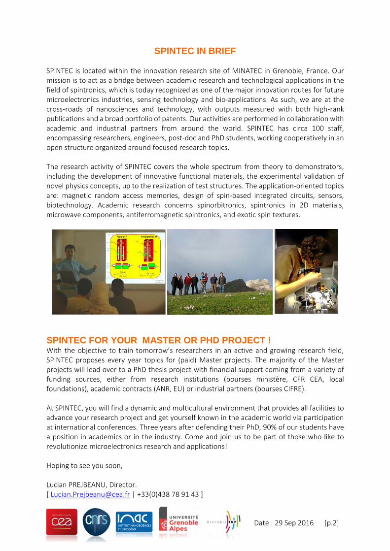
SPINTEC IN BRIEF SPINTEC is located within the innovation research site of MINATEC in Grenoble, France. Our mission is to act as a bridge between academic research and technological applications in the field of spintronics, which is today recognized as one of the major innovation routes for future microelectronics industries, sensing technology and bio-applications. As such, we are at the cross-roads of nanosciences and technology, with outputs measured with both high-rank publications and a broad portfolio of patents. Our activities are performed in collaboration with academic and industrial partners from around the world. SPINTEC has circa 100 staff, encompassing researchers, engineers, post-doc and PhD students, working cooperatively in an open structure organized around focused research topics. The research activity of SPINTEC covers the whole spectrum from theory to demonstrators, including the development of innovative functional materials, the experimental validation of novel physics concepts, up to the realization of test structures. The application-oriented topics are: magnetic random access memories, design of spin-based integrated circuits, sensors, biotechnology. Academic research concerns spinorbitronics, spintronics in 2D materials, microwave components, antiferromagnetic spintronics, and exotic spin textures.
SPINTEC FOR YOUR MASTER OR PHD PROJECT ! With the objective to train tomorrow’s researchers in an active and growing research field, SPINTEC proposes every year topics for (paid) Master projects. The majority of the Master projects will lead over to a PhD thesis project with financial support coming from a variety of funding sources, either from research institutions (bourses ministère, CFR CEA, local foundations), academic contracts (ANR, EU) or industrial partners (bourses CIFRE). At SPINTEC, you will find a dynamic and multicultural environment that provides all facilities to advance your research project and get yourself known in the academic world via participation at international conferences. Three years after defending their PhD, 90% of our students have a position in academics or in the industry. Come and join us to be part of those who like to revolutionize microelectronics research and applications! Hoping to see you soon, Lucian PREJBEANU, Director. [ [email protected] | +33(0)438 78 91 43 ]
Date : 29 Sep 2016 [p.3]
TOPICS FOR MASTER AND PHD PROJECTS
MRAM MEMORIES 1 Double magnetic tunnel junctions suitable for automotive memory applications
2 Thermally assisted writing of magnetic memory cell (MRAM) by spin polarized
3 Memristive magnetic memories for spintronics synapses
Magnetic Sensors 4 Ultra-sensitive magnetic field sensors for space application
HEALTH AND BIOLOGY 5 Elaboration of biocompatible magnetic microparticles for cancer cells destruction
MICROWAVE DEVICES
6 Magnonics
7 Characterisation of spintorque oscillators
8 Développement d'un magnétomètre durci aux irradiations
2D SPINTRONICS 9 Tuning spin-orbit coupling in silicon and germanium for spin generation, detection and
manipulation
ANTIFERROMAGNETIC SPINTRONICS 10 Antiferromagnetic materials and spintronics
SPIN TEXTURES 11 Electroless deposition of magnetic nanotubes and core-shell nanowires for a 3D spintronics
12 High-resolution TEM magnetic imaging of nanotubes for spintronics
THEORY AND SIMULATION 13 Finite element modeling for spintronics

Date : 29 Sep 2016 [p.4]
Date : 29 Sep 2016 [p.5]
Stage N° : 1 Contact Ricardo SOUSA, [email protected] , +33 4.38.78.48.95 Bernard DIENY, [email protected] , +33 4.38.78.38.70 DOUBLE MAGNETIC TUNNEL JUNCTIONS SUITABLE FOR AUTOMOTIVE MEMORY APPLICATIONS Keywords Magnetic memory ; MRAM ; STT-MRAM ; magnetic tunnel junctions Summary There is an increase interest in microelectronics industry for a new type of magnetic non-volatile memory called STT-MRAM. In these memories the storage elements are magnetic tunnel junctions which consist of two ferromagnetic layers separated by a thin tunnel oxide barrier (MgO). They are about to be introduced in products for consumer electronics. It is envisioned that they could play also a very important role in industrial and automotive applications but for the latter, the specifications are much more stringent in terms of reliability and operating temperatures (up to 150°C instead of 80°C for consumer electronics). In this internship and possibly the subsequent thesis project, we propose to explore several routes allowing to increase the performances of these memories in terms of switching speed, power consumption and operating range. Details of subject The advent of STT-MRAM in microelectronics industry represent a major breakthrough which will significantly contribute to reducing the power consumption of electronic circuits. STT-MRAM are non-volatile memories based on magnetic tunnel junctions (MTJ). MTJ consist of two ferromagnetic layers separated by a very thin MgO tunnel barrier (1nm thick). The information is encoded in the magnetic orientation of one of the layer (called storage layer) while the magnetization of the other layer remains fixed. When a current flows through the junction, the resistance depends of the relative orientation of the magnetization of the two magnetic layers (Parallel=”0”=low resistance state; antiparallel=”1”=high resistance state). During write, the magnetic state of the storage layer is switched by a phenomenon called spin transfer torque which results from the exchange interaction between the spin of the tunneling electrons and those responsible for the magnetization of the storage layer. SPINTEC played a leading role in the development of magnetic memories based on these structures which are now about to be widely adopted by the microelectronic industry. For some applications, further work is however still needed to increase the switching speed (to reach the ns regime with high reliability), to reduce the write current for downsize scalability and to increase the temperature operating range. In this internship, we propose to study double barrier magnetic tunnel junctions with double polarizers. Compared to the structures developed so far, those should have higher performances in terms of thermal stability of the storage layer magnetization against thermal fluctuations (i.e. improved memory retention) and larger spin transfer torque efficiency allowing lower write current. Based on the previous experience of our laboratory, we propose to grow this type of stacks by sputtering, characterize their magnetic properties as

Date : 29 Sep 2016 [p.6]
well as their electrical properties at wafer level. We will then pattern the stacks in the form of nanometric pillars in our clean room and characterize their switching by spin transfer torque. The results will be benchmarked with the properties of the existing structrues. We hope that the internship will be pursued in a thesis. This would allow a thorough optimization of the stack to reach specifications compatible for automotive and industrial applications Requested skills Basics in programming and magnetism Possibility to follow with a PhD Yes
Date : 29 Sep 2016 [p.7]
Stage N° : 2 Contacts Ricardo SOUSA ([email protected]; +33 4.38.78.48.95) Title THERMALLY ASSISTED WRITING OF MAGNETIC MEMORY CELL (MRAM) BY SPIN POLARIZED CURRENT Keywords Magnetic memory ; MRAM ; STT-MRAM ; magnetic tunnel junctions Summary Magnetic MRAM combine non-volatility and write speed of a few nanoseconds. The more advanced concepts MRAM use current pulses to switch between two states of resistance. A patented thermally-assisted writing approach, allows the production of memory cells with better retention. The stability of the cell is temporarily reduced during the write step by the heating produced by the current flow, which allows obtaining a better tradeoff between retention and consumption. The internship goal is to characterize and evaluate the simultaneous use of a spin polarized current and a controlled heating to orient the magnetization of the storage layer of an MRAM memory element. The objective is to obtain the steepest possible temperature dependence of the magnetic anisotropy at the write temperature. At the same time, one must ensure that when writing, the magnetic configuration is stable during and after the write pulse. The work will consist in identifying the conditions to avoid write errors during the cooling of the junction. This analysis may be performed using electrical devices measures, and also by a macrospin modeling taking into account the thermal variations in material parameters. This work can be pursued during a PhD thesis in collaboration with Crocus Technology (CIFRE). Details of subject Magnetic MRAM combine non-volatility and write speed of a few nanoseconds. The more advanced concepts MRAM use current pulses to switch between two states of resistance. A patented thermally-assisted writing approach, allows the production of memory cells with better retention. The stability of the cell is temporarily reduced during the write step by the heating produced by the current flow, which allows obtaining a better tradeoff between retention and consumption. The internship goal is to characterize and evaluate the simultaneous use of a spin polarized current and a controlled heating to orient the magnetization of the storage layer of an MRAM memory element. The objective is to obtain the steepest possible temperature dependence of the magnetic anisotropy at the write temperature. At the same time, one must ensure that when writing, the magnetic configuration is stable during and after the write pulse. The work will consist in identifying the conditions to avoid write errors during the cooling of the junction. This analysis may be performed using electrical devices measures, and also by a macrospin modeling taking into account the thermal variations in material parameters. This work can be pursued during a PhD thesis in collaboration with Crocus Technology (CIFRE). References and further reading:
Date : 29 Sep 2016 [p.8]
[1] S. Bandiera, R.C. Sousa et al., Appl. Phys. Lett., 99, 202507 (2011) [2] A. A. Timopheev, R. Sousa, M. Chshiev, L. D. Buda-Prejbeanu, and B. Dieny, Phys. Rev. B 92, 104430 (2015) Requested skills Basics in programming and magnetism Possibility to follow with a PhD Yes
.
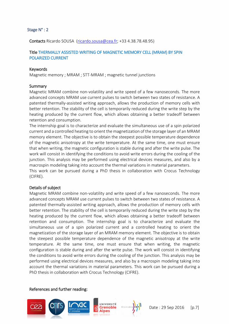
Fig. 1 : Images of magnetic tunnel junction and magnetic nano-pilar. The graph represents the switching of the resistance state of an MRAM cell, performed by 50ns current pulses. The pulse polarity is alternated at each successive pulse.

Date : 29 Sep 2016 [p.9]
Stage N° : 3 Contact Liliana BUDA-PREJBEANU, [email protected], +33 4.38.78.44.19 Bernard DIENY, [email protected] , +33 4.38.78.38.70 Title MEMRISTIVE MAGNETIC MEMORIES FOR SPINTRONICS SYNAPSES Keywords Memristors ; synspases ; Magnetic memory ; neuromorphic ; magnetic tunnel junctions Summary Conventional electronic circuits consume much more energy than human brain at comparable performances. Consequently, there is a strong interest in developing electronic circuits which mimic the working principle of the brain. These circuits are particularly suited for learning functions, associative functions, pattern recognition etc. For that purpose, it is necessary to develop new electronic components which realize neurons or synaptic functions. Synapses are interconnection elements between neurons able to keep the memory of the history of the current pulses to which that have been submitted. In this internship, we propose to develop such electronic synapses based on spintronics phenomena and particularly the tunnel magnetoresistance of magnetic tunnel junctions. The component resistance will continuously vary from a minimal to a maximal value depending on the succession of current pulses through it. The internship will comprise micromagnetic simulations as well as material developments. We wish that it will be pursued in a thesis. Details of subject In electronics, there is a rising interest for developing new circuits called “neuromorphics” which mimic the working principle of the brain. Those can perform complex operations with must less power consumption than conventional electronic circuits (cf chess game opposing the worldwide chess champion (<20W) to IBM supercomputer (>1MW)). In this context, the purpose of the internship is to develop a new type of spintronics components realizing synaptic functions. The resistance of such component must continuously vary between a minimum and maximum value depending on the succession of current pulses sent though the component. Such components are called memristor (Memory Resistor). Today, in the field of spintronics, a first category of such component was developed based on magnetic domain wall displacements [1]. Here, we propose to investigate for the first time a new class of such components based on the angular orientation of the storage layer magnetization in magnetic tunnel junctions. This type of junctions are already used in a binary way for binary memory functions (MRAM or STT-MRAM). We propose to modify the working principle of these junctions to be able to reach all intermediate states between Rmin and Rmax thus realizing the memristor function. The internship will comprise micromagnetic simulations and material development. The storage layer magnetization dynamics will be studied by micromagnetic simulations based on Landau Lifshitz Gilbert equation including spin transfer torque terms. The numerical study will then comprise two stages: a) identification of a type of material for the storage layer of the magnetic tunnel junction which will allow to stabilize the magnetization in all directions in the plane of the layer. Demonstration by micromagnetic simulations of the
Date : 29 Sep 2016 [p.10]
possibility to rotate the magnetization by successive steps clockwise or anticlockwise depending on the pulsed current direction. b) Analysis of the thermal stability of the magnetization in this device submitted to thermal fluctuations. On the experimental side, we will develop an isotropic coercitive material for the storage layer of the magnetic tunnel junction and characterize its magnetic properties. All the numeric tools and experimental equipment required for this study are available at SPINTEC. We wish this internship to be pursued in a thesis. The thesis will allow to build the whole device, test its synaptic behavior and incorporate it in simple neuromorphic circuits. [1] N. Locatelli et al. Spin-torque building blocks Nature Materials 13, 11 (2014) Requested skills Basics in programming and magnetism Possibility to follow with a PhD Yes
Date : 29 Sep 2016 [p.11]
Stage N° : 4 Contact Claire Baraduc ([email protected], +33 438784235) Title ULTRASENSITIVE MAGNETIC FIELD SENSOR FOR SPACE APPLICATIONS Keywords magnetic sensors, magnetic tunnel junctions Summary Magnetic sensors for space flight are highly sensitive inductive sensors but they are cumbersome and heavy (150g/axis) which impacts the launching cost. Since many years, research has been performed in order to reduce the sensor size and mass. However no further progress is expected on this line without a definite change of paradigm. The solution could be spintronic devices provided they could present the proper sensitivity. We are therefore developing a magnetic sensor which combines an innovative architecture with a low-noise magneto-resistive element. Our objective is to improve the sensor performances by including an innovative magnetic tunnel junction that we intend to protect with a patent. The experimental work will be : i)the microfabrication of the device; ii) measurement of the electrical noise ; the unction composition and geometry will be optimized by numerical simulations. Details of subject The aim of this project is to manufacture a magnetic sensor that could be a serious competitor, in term of sensitivity, to those currently shipped onboard the space missions, with a weight reduction of at least two orders of magnitude. Up to now, magnetic field sensor used for space missions are inductive magnetic sensors that have a very high sensitivity, up to few tenths of fT. Nevertheless, this very good sensitivity is achieved at the cost of large size and mass (150g per axis), markedly increasing the launching cost. Solutions to reduce the sensor mass has been systematically tested for years but no further improvement can now be obtained without a change of paradigm. Using nano-devices from spin electronics integrated on silicon would allow a significant progress in the size and mass reduction of vectorial magnetic sensors provided they could have the required sensitivity. We are therefore developing an ultra-sensitive magnetic sensor that combines an innovative architecture and a low noise magneto-resistive element. It includes a magnetic circuit, a biasing coil and a tunnel junction, made with thin film technology, an electronic circuit in ASIC technology and a feed-back coil made with a micro winding process, the latter responsible for the sensor high performance in terms of linearity and stability. The sensor high sensitivity is obtained by a strong amplification (>300) of the measured magnetic field thanks to the magnetic circuit acting as a flux concentrator, and by using magnetic tunnel junctions with high magnetoresistive ratio. The originality of the proposed sensor lies in a differential and heterodyne detection combined with a feed-back: the magnetic field to be measured is modulated by an ac biasing field, so that the measurement is translated in the vicinity of the biasing frequency where the noise is low. Our objective is now to improve the quality of the flux concentrator by the choice of materials (laminated NiFe layer, multilayer with antiferromagnetic coupling or amorphous alloys) and to replace the current tunnel junction by an innovative junction (patent in progress). Optimizing the new junction will require

Date : 29 Sep 2016 [p.12]
numerical simulations and experimental tests. The innovative and ambitious features of the proposed solution should allow to develop a sensor able to detect magnetic fields as low as 100fT/Hz1/2 in the frequency range below 10kHz, which corresponds to a sensitivity three orders of magnitude larger than the best magnetoresistive sensors currently available. Furthermore, a large reduction in size increases the sensor spatial resolution which extends the scope of applications towards the medical sector, biotechnologies or non destructive control for example Requested skills solid state physics Possibility to follow with a PhD Yes
Date : 29 Sep 2016 [p.13]
Stage N° : 5 Contact Robert Morel, [email protected], 04.38.78.55.03 Title ELABORATION OF BIOCOMPATIBLE MAGNETIC MICROPARTICLES FOR CANCER CELLS
DESTRUCTION
Keywords Biomedical applications, magnetic clusters, cancer cells apoptosis Summary The CEA/INAC SPINTEC lab offers an internship opportunity on the development of a new
method for the synthesis of magnetic particles aimed at biomedical applications, for targeted
cancer cells killing. The approach we are developing consists in inducing apoptosis
(spontaneous death) in tumor cells via vibration of magnetic nanoparticles attached to the
cell membrane, by applying a rotating magnetic field.
Identification of the anti-tumor effect associated with mechanical vibrations has been
achieved in 2010 and, since, there have been several studies on this topic in our lab, in
particular on the synthesis of dedicated magnetic particles – using techniques borrowed from
microelectronics – and their functionalization. The likely applicability of these particles for
cancer therapy have been demonstrated, using in vitro experiments, in a recently defended
doctorate thesis in our research team. However, the extension of in-going work to in vivo
studies – for which larger amount of biocompatible particles is needed – requires to develop
new processes for their fabrication. The synthesis route we are proposing is based on
mechanical alloying.
Details of subject The purpose of this internship is to develop the synthesis of magnetite (Fe3O4) magnetic
particles using mechanical grinding. This material is chosen primarily for its biocompatibility,
opening the possibility of clinical use. More specifically, the candidate will define the
grindings conditions to obtain, from a given magnetite powder, non - spherical particles with
a size of about one micrometer. The study of the particles will comprize scanning electron
microscopy and the measure of ensemble magnetic properties by VSM and SQUID
magnetometry. The data collected will serve as input for the analytical or numerical
simulations calculations of the intrinsic magnetic properties of the particle, and the
mechanical forces exerted during the application of a variable magnetic field.
One constraint for the development of magnetic particles for biomedical applications is the
need to disperse them in the liquid phase. Indeed, both the magnetic forces between
particles and the chemical or electrostatic interactions, either short or long range, promote
clustering. Part of the work will be devoted to the study of these effects, firstly by defining

Date : 29 Sep 2016 [p.14]
the optimal magnetic properties – with regards with the shape and size - and secondly by
developing a protocol for the dispersion of particles by sonication.
The extension of this study in a doctorate thesis following the internship, subject to funding,
will comprize 1) the development of a process for surface functionalization to ensure, in
addition to the dispersion of particles when in solution, the binding selectivity on targeted
cancer cells membrane; 2) preliminary studies regarding toxicity and mechanical response
under applied magnetic field; 3) in vitro testing to assess the ability of these new particles to
induce apoptosis in cancer cells; 4) participation in the in vivo tests on glioblastoma tumors
with these biocompatible particles.
Requested skills This internship is intended for M2 students. The expected background for the candidate is a multi-disciplinary degree in nanosciences and nanotechnologies covering both physics and biology. Possibility to follow with a PhD Yes
Date : 29 Sep 2016 [p.15]
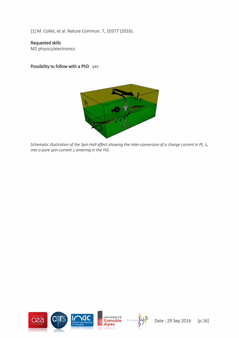
Stage N° : 6 Contact Olivier Klein ([email protected] ; +33 4 38 78 58 02) Title MAGNONICS Keywords Magnetic resonance, microwaves, metrology Summary The aim of this internship is to study new devices exploiting the propagation of pure spin current in electrical insulators. One of the expected benefits over conventional electronic devices are a significant reduction in energy consumption thanks to the absence of Joule heating. We will study in particular SWASER effect (or spin-wave amplification by stimulated Emission radiation), which consists of spontaneously emitting magnon by continuously pumping spins inside the magnetic material from the interface. The purpose of this internship will be a fundamental study of nonlinear couplings and competition between own propagation modes. In particular, try to minimize these effects playing on the magnetic configuration. Details of subject Magnonic is an emerging research field, which aims at exploiting pure spin transport in magnetic materials. The elementary excitations are the propagating spin-waves, also called magnon, which are bosonic quasiparticles. The advantages over conventional electronic devices are a significant reduction in energy consumption thanks to the absence of Joule heating, as well as new features taking advantage of the wave-particle duality. Magnetic materials could be electrical insulators, knowing that their dynamical characteristics are usually much better than their metal counterparts. Among all magnetic insulators, yttrium iron garnet (YIG or Y3Fe5O12) holds a special place for having the lowest known damping factor in nature. This theme has attracted recently a lot of attention since the discovery of the spin Hall effect, which capitalizes on the deflection of the electron trajectory according to their spin orientation. When a charge current (Jc) is flowing in a normal metal of strong spin-orbit coupling such as platinum (Pt) it converts into a pure spin current (Js), propagating in the perpendicular direction, where the conversion efficiency is set by the spin Hall angle (see FIG1), which can then eventually cross the interface matal/insulator. The striking signature of the spin transfer process would be the emission of microwave radiation when the system is pumped out of equilibrium by a d.c. current (FIG1). Since the spin transfer torque on the magnetization is collinear to the damping torque, an instability threshold occurs when the natural damping is fully compensated by the external flow of angular momentum, leading to spin-wave amplification through stimulated emission. Using analogy to light, the effect was called spin-wave amplification by stimulated emission of radiation (SWASER). In this training the objectives are a fundamental study on the non-linear effects and mode competition between the eigen-states of the system, which are responsible for self-limiting effects. The devices are going to be YIG stripes patterned by standard technics of nano-lithography at the PTA of the CEA-Grenoble. Reference :
Date : 29 Sep 2016 [p.16]
[1] M. Collet, et al. Nature Commun. 7, 10377 (2016). Requested skills M2 physics/electronics Possibility to follow with a PhD yes
Schematic illustration of the Spin Hall effect showing the inter-conversion of a charge current in Pt, Jc, into a pure spin current Js entering in the YIG.
Date : 29 Sep 2016 [p.17]
Stage N° : 7 Contact Ursula Ebels ([email protected]; +33 4 38 78 53 44) Title CHARACTERISATION OF SPINTORQUE OSCILLATORS Keywords : Spintronics, magneto-resistive devices, magnetization dynamics Summary One of the basic concepts of spintronics is the spin momentum transfer where spin polarized conduction electrons can transfer a magnetic moment to the local magnetization of a thin ferromagnetic film. This magnetic momentum transfer is responsible for the excitation of high frequency (Gigahertz range) magnetization oscillations when a DC current is injected into a magneto-resistive device. SPINTEC studies these effects of spin momentum transfer from a fundamental point of view to better understand the non-linear magnetization dynamics of nansocale devices, but also in context of potential applications for the development of integrated microwave components. In particular, the effect can be used to generate microwave signals as well as to detect microwave signals. The combination of the two could lead to a novel concept for a wireless communication system, which is the object of study of this internship, followed by a PhD thesis. Details The non-linear dynamics of a spin transfer torque oscillator and its microwave signal generation have been studied in the past by our group as well as by numerous others. Good results in terms of output power and spectral purity have been obtained for oscillators emitting in the 0.2-1GHz range. Operation at higher frequency ranges (1-10GHz) of interest for applications, still suffers from too high a phase noise, making implementation for instance into a phase locked loop (PLL) difficult. The aim of the present internship project, followed by a PhD, is to explore different magnetic stack configurations (magnetization in-plane and/or out of plane for polarizer and/or free layer), allowing for more stable and robust oscillations. The final aim is the operation and characterization of a PLL for the frequency range of 1-10GHz. A second goal is the exploration of a wireless short range communication concept that is based on the emission of electromagnetic waves via spin torque oscillators and the detection of this wave by a second spin transfer device. In the first part of the project, the student will carry out numerical simulations. This will be followed by the realization of the devices (materials deposition and nanofabrication) and the characterization of the high frequency response of the devices. This work will be carried out in collaboration with the microwave components team of Spintec as well as in collaboration with TU Dresden (for PLL testing)

Date : 29 Sep 2016 [p.18]
Requested skills Master M1 or M2; Motivated student with a sound background in solid state physics and/or nanosciences and keen to explore new concepts and ideas that are at the interface between physics (spintronics) and applications (microwave oscillators). Possibility to follow with a PhD: Yes
Date : 29 Sep 2016 [p.19]
Stage N° : 8 Contact Olivier Klein ([email protected] ; +33 4 38 78 58 02) Titre DEVELOPPEMENT D'UN MAGNETOMETRE DURCI AUX IRRADIATIONS Mots Clés résonance magnétique, micro-onde, métrologie Résumé Le but du stage est de construire un magnétomètre à résonance ferromagnétique. Son principe est basé sur l'effet gyromagnétique où l'intensité du champ magnétique appliqué est proportionnelle à la fréquence de précession de l'aimantation. L'objectif sera de construire un oscillateur asservit à la résonance ferromagnétique puis de mesurer avec précision la fréquence de Larmor. L'élément magnétique sera une sphère de YIG. On mesurera ses performances et on testera sa sensibilité aux irradiations que l'on comparera à celles d'une sonde à effet Hall. Détails du sujet Il existe actuellement un besoin pour des magnétomètres précis capable de mesurer dans un environnement ionisant la valeur du champ magnétique sur une très large gamme de champ. Le but de ce stage sera de développer un magnétomètre à résonance ferromagnétique dont le principe est basé sur l'équation de Kittel pour une sphère 2πf=1/3γH0, où f est la fréquence de précession, H0 est le champ magnétique appliqué et γ est le rapport gyromagnétique. Ainsi l'intensité du champ magnétique sera codée dans la fréquence de précession de l'aimantation. L'objectif du stage sera de développer un prototype de laboratoire dont on évaluera les performances. Ce projet se fera en collaboration avec la société Caylar, une PME spécialisée dans la métrologie qui souhaite ultérieurement commercialiser une telle sonde. Des campagnes de mesure sur l'endurcissement aux irradiations seront prévues. Un premier objectif sera d'atteindre une précision inférieure à 100ppm en utilisant une sphère de YIG. Compétences requises M1 ou M2 physique/électronique Poursuite par une thèse Oui

Date : 29 Sep 2016 [p.20]
Date : 29 Sep 2016 [p.21]
Stage N° : 9 Contact Matthieu [email protected], +33-438782262 Title
TUNING SPIN-ORBIT COUPLING IN SILICON AND GERMANIUM FOR SPIN GENERATION, DETECTION AND MANIPULATION
Keywords Spintronics, semiconductors, silicon, germanium, spin-orbit coupling Summary The aim of semiconductor spintronics is to use the electron spin in addition to its charge in microelectronics devices. The spin degree of freedom adds new functionalities to existing devices and will allow to reduce power consumption. The three requirements for the development of such technology are the generation, detection and manipulation of spin polarized electrons in Si or Ge (the materials of today’s microelectronics). A new paradigm has recently raised in the spintronics community which consists in using the spin-orbit coupling to complete those three operations. The spin-orbit coupling couples the electron momentum and spin. Hence, it makes possible the spin manipulation by electric fields but also the inter-conversion between charge currents and spin currents by the spin Hall effect in bulk materials or the Rashba effect at interfaces. Unfortunately, in bulk Si and Ge, the spin-orbit coupling is too weak and this is the objective of this internship and following thesis work to study ways to enhance it. First, we will focus on metal/Si(111) and Ge(111) interfaces where the Rashba spin-orbit coupling is predicted very strong. Then, two more promising systems will be investigated: topological insulator/Si(111) and Ge(111) interfaces as well as Si and Ge thin films doped with heavy atoms. The candidate will benefit from the long standing experience of our group in semiconductor spintronics and from the close collaboration with the CEA LETI. Details of subject The aim of semiconductor spintronics is to use the electron spin in addition to its charge in microelectronics devices. The spin degree of freedom adds new functionalities to existing devices and will allow to reduce power consumption. The first requirement for the development of semiconductor spintronics is to generate a population of spin polarized electrons in silicon or germanium, the materials of today’s microelectronics. This out-of-equilibrium spin population will diffuse into the semiconductor creating a spin current. In our laboratory, we managed to generate and detect electrically, from a ferromagnetic electrode, a spin accumulation and current in Si and Ge at room temperature. The next step for the development of semiconductor spintronics is the spin manipulation. Magnetic fields can be used to manipulate the spin state but they cannot be easily implemented in microelectronics. Instead, the spin can be manipulated by electric fields in combination with the spin-orbit coupling. However, Si and Ge are rather light atoms with weak spin-orbit coupling preventing any efficient spin manipulation by electric fields. During this internship and the following thesis work, we will propose new strategies to enhance the spin-orbit coupling in Si and Ge to manipulate the spin but also to generate and detect spin currents. First, we will study the two-dimensional spin transport into the Rashba states at metal/Si(111) and metal/Ge(111)
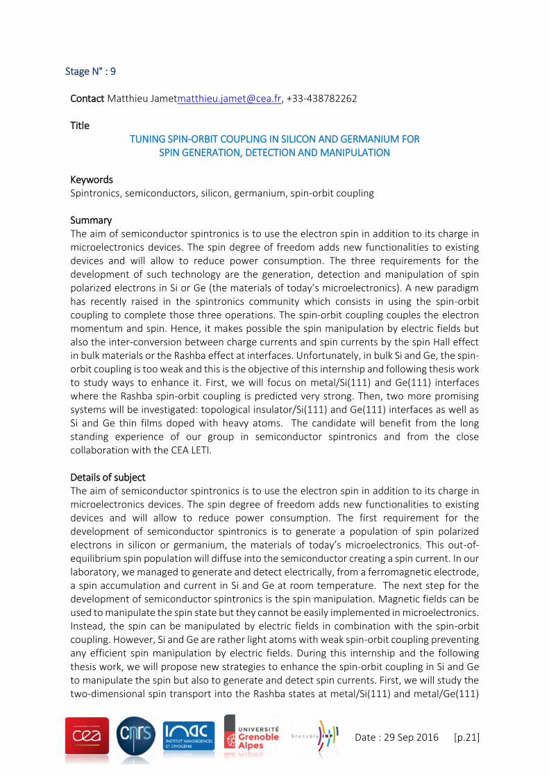
Date : 29 Sep 2016 [p.22]
interfaces where the Rashba spin-orbit coupling is predicted to be very strong. In this case, the electric field originates from the crystal symmetry breaking at the interface. Moreover, the Rashba spin-orbit coupling is so strong that it becomes possible to generate a spin current from a charge current and vice-versa into the interface states at room temperature. Hence, we will explore a new paradigm in semiconductor spintronics: the use of spin-orbit coupling instead of ferromagnetic electrodes to generate and detect spin currents in Si and Ge. During the PhD thesis, other systems will also be investigated like Si and Ge doped with heavy atoms to induce large bulk spin-orbit coupling and topological insulators grown on Ge(111) or Si(111) in which surface states allow for efficient spin-to-charge inter-conversion. To do this, the student will benefit from the experience of our team in semiconductor spintronics and in the fabrication of nanodevices made of Si and Ge as shown in the figure. A cryostat (2K-300K, 0-7 Tesla) will also be available specifically for these experiments. An electron paramagnetic resonance spectrometer will be used to perform dynamical spin injection into silicon and germanium from a ferromagnetic electrode at resonance. The candidate will also benefit from all the equipments available at Spintec and from the close collaboration with the CEA LETI in Grenoble and Unité Mixte CNRS THALES in Palaiseau. This work will be financially supported by the French Research Agency project TOP-RISE. Requested skills Solid state physics, spintronics and nanomagnetism Material growth by molecular beam epitaxy, semiconductor physics, surface and interface science Possibility to follow with a PhD Yes
Date : 29 Sep 2016 [p.23]
Stage N° : 10 Contact : BALTZ Vincent ([email protected], +33 4 38 78 03 24) Title : ANTIFERROMAGNETIC MATERIALS AND SPINTRONICS Keywords: spintronics, nanomagnetism; antiferromagnetic order Summary Antiferromagnetic materials (antiparallel alignment of the atomic magnetic moments) could represent the future of spintronic applications thanks to the numerous interesting features they combine: they are robust against perturbation due to magnetic fields, produce no stray fields, display ultrafast dynamics and are capable of generating large magneto-transport effects. Intense research efforts are being invested in unraveling spin-dependent transport properties in antiferromagnetic materials. Whether spin-dependent transport can be used to drive the antiferromagnetic order and how subsequent variations can be detected are some of the thrilling challenges to address. Details of subject The purpose of this internship is to study the spin dependent properties and functionalities of antiferromagnetic materials. The main challenges are to quantify and understand the spin-dependent transport in antiferromagnetic materials and particularly the parameters that govern it. The nature of the elements constituting the antiferromagnetic material and the quality of the interfaces will be the adjustable parameters. We will consider mainly the efficiency of spin injection and the interfacial filtering, the absorption of spins in the core of the material and the absorption characteristics lengths, the order temperatures and the magnetic susceptibility, and the efficiency of the spin-orbit coupling via the spin Hall effect. This internship is experimental. It will build on the many techniques of fabrication and characterization at SPINTEC and benefit from the collaboration with the SYMMES/RICC CEA laboratory for experiments with a resonant cavity. For more information on antiferromagnetic spintronics, feel free to visit the following link, which reviews research conducted around the world on this theme: http://arxiv.org/abs/1606.04284 Requested skills Master M2 (materials science, solid state physics), fluent in English or French Possibility to follow with a PhD Yes

Date : 29 Sep 2016 [p.24]
Date : 29 Sep 2016 [p.25]
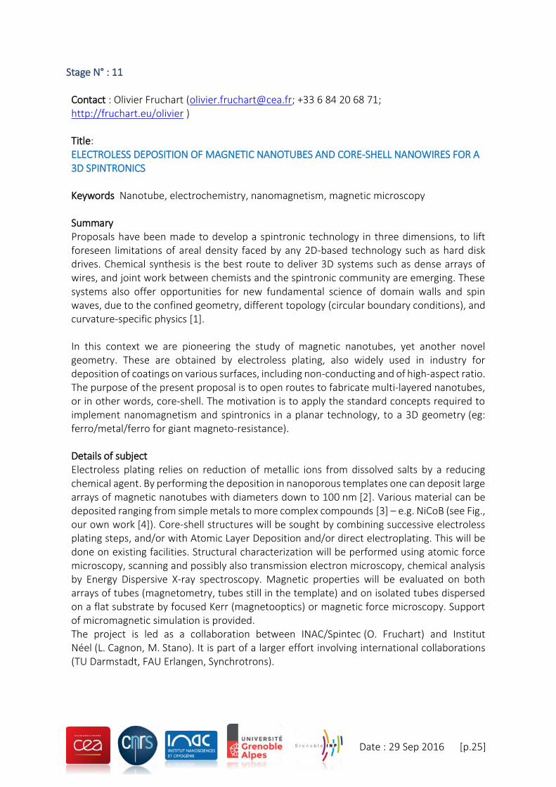
Stage N° : 11 Contact : Olivier Fruchart ([email protected]; +33 6 84 20 68 71; http://fruchart.eu/olivier ) Title: ELECTROLESS DEPOSITION OF MAGNETIC NANOTUBES AND CORE-SHELL NANOWIRES FOR A 3D SPINTRONICS Keywords Nanotube, electrochemistry, nanomagnetism, magnetic microscopy Summary Proposals have been made to develop a spintronic technology in three dimensions, to lift foreseen limitations of areal density faced by any 2D-based technology such as hard disk drives. Chemical synthesis is the best route to deliver 3D systems such as dense arrays of wires, and joint work between chemists and the spintronic community are emerging. These systems also offer opportunities for new fundamental science of domain walls and spin waves, due to the confined geometry, different topology (circular boundary conditions), and curvature-specific physics [1]. In this context we are pioneering the study of magnetic nanotubes, yet another novel geometry. These are obtained by electroless plating, also widely used in industry for deposition of coatings on various surfaces, including non-conducting and of high-aspect ratio. The purpose of the present proposal is to open routes to fabricate multi-layered nanotubes, or in other words, core-shell. The motivation is to apply the standard concepts required to implement nanomagnetism and spintronics in a planar technology, to a 3D geometry (eg: ferro/metal/ferro for giant magneto-resistance). Details of subject Electroless plating relies on reduction of metallic ions from dissolved salts by a reducing chemical agent. By performing the deposition in nanoporous templates one can deposit large arrays of magnetic nanotubes with diameters down to 100 nm [2]. Various material can be deposited ranging from simple metals to more complex compounds [3] – e.g. NiCoB (see Fig., our own work [4]). Core-shell structures will be sought by combining successive electroless plating steps, and/or with Atomic Layer Deposition and/or direct electroplating. This will be done on existing facilities. Structural characterization will be performed using atomic force microscopy, scanning and possibly also transmission electron microscopy, chemical analysis by Energy Dispersive X-ray spectroscopy. Magnetic properties will be evaluated on both arrays of tubes (magnetometry, tubes still in the template) and on isolated tubes dispersed on a flat substrate by focused Kerr (magnetooptics) or magnetic force microscopy. Support of micromagnetic simulation is provided. The project is led as a collaboration between INAC/Spintec (O. Fruchart) and Institut Néel (L. Cagnon, M. Stano). It is part of a larger effort involving international collaborations (TU Darmstadt, FAU Erlangen, Synchrotrons).
Date : 29 Sep 2016 [p.26]
References: [1] Streubel et al., J. Phys. D: Appl. Phys. 49 , 363001 (2016). [2] Li et al., CrystEngComm 16, 4406 (2014). [3] Richardson et al., ECS Trans. 64 (31), 39-48 (2015). [4] Schaefer et al., RSC Adv., 6, 70033 (2016) Requested skills Physics/Chemistry at bachelor level. A taste for experimental and multidisciplinary work is appreciated. Welcome: physical chemistry, nanomagnetism, characterization techniques Possibility to follow with a PhD Yes (preferred)
Figure 1: NiCoB tube, from the left: structure+XMCD-PEEM (X-ray Magnetic Circular Dichroism Photo-Emission Electron Microscopy), Transmission electron microscopy.
Date : 29 Sep 2016 [p.27]
Stage N° : 12 Contact Dr J. L Rouvière, [email protected], 0438785086 (CEA/INAC/LEMMA) Co-advisors : E. Gautier, [email protected]; O. Fruchart (SPINTEC) Title HIGH-RESOLUTION TEM MAGNETIC IMAGING OF NANOTUBES FOR SPINTRONICS Keywords TEM, magnetic imaging, nanotubes, simulation, micromagnetism Summary The objective of the internship is the study by transmission electron microscopy (TEM) of magnetic nanotubes chemically synthesized. We are studying these as models objects to explore the concept of information storage in a 3D magnetic media, based on the propagation of magnetic walls along one-dimensional structures. Physico-chemical study of the material and magnetic imaging at the nanometer scale will be used to explore and understand the arrangement of domains and domain walls in these systems, whose synthesis has been achieved recently. The experimental techniques used are the chemical and structural analysis by electron diffraction and high-resolution imaging, magnetic imaging and electron holography, in a transmission electron microscope. The student will perform sample preparation for electron microscopy, the installation of a device for an observation in the microscope, and imaging. The work also includes an aspect of processing, interpretation of data and participation in micro-magnetic simulations to assist physical understanding. These will be done in collaboration with the laboratory of simulation group SPINTEC / NEEL. Details of subject To perform the structural and magnetic microscopy we benefit from the latest and world-leading equipment for chemical analysis, images of matter at the atomic scale and also to visualize magnetic fields. The work will be largely experimental: - The chemical and structural analysis by electron diffraction - The high-resolution images - The magnetic imaging and electron holography with a resolution of a few nanometers. The experimental systems are under control, and will be made available. In preliminary experiments with photoelectron microscopy (PEEM, experiments with synchrotron radiation) we evidenced orthoradial domains, thus with flux-closure. This closure is very interesting in the context of a 3D memory because it minimizes the effects of long-range dipolar fields, and thus cross-talk between elements. However it is unexpected with respect to the axial direction. Following this, in this internship we will try to clarify the reason for this orientation, in connection with the microstructure. Moreover, thanks to our high spatial resolution we will seek to clarify the type of magnetic walls occurring between the domains, which have a crucial impact on their dynamics expected in a magnetic field or spin-polarized current. The student will develop sample preparation for electron microscopy (dispersion of tubes initially in solution, possible use of etching by focused ion beam), installation of a device for observation in the microscope. Static studies, possibly in magnetic field or high temperature,
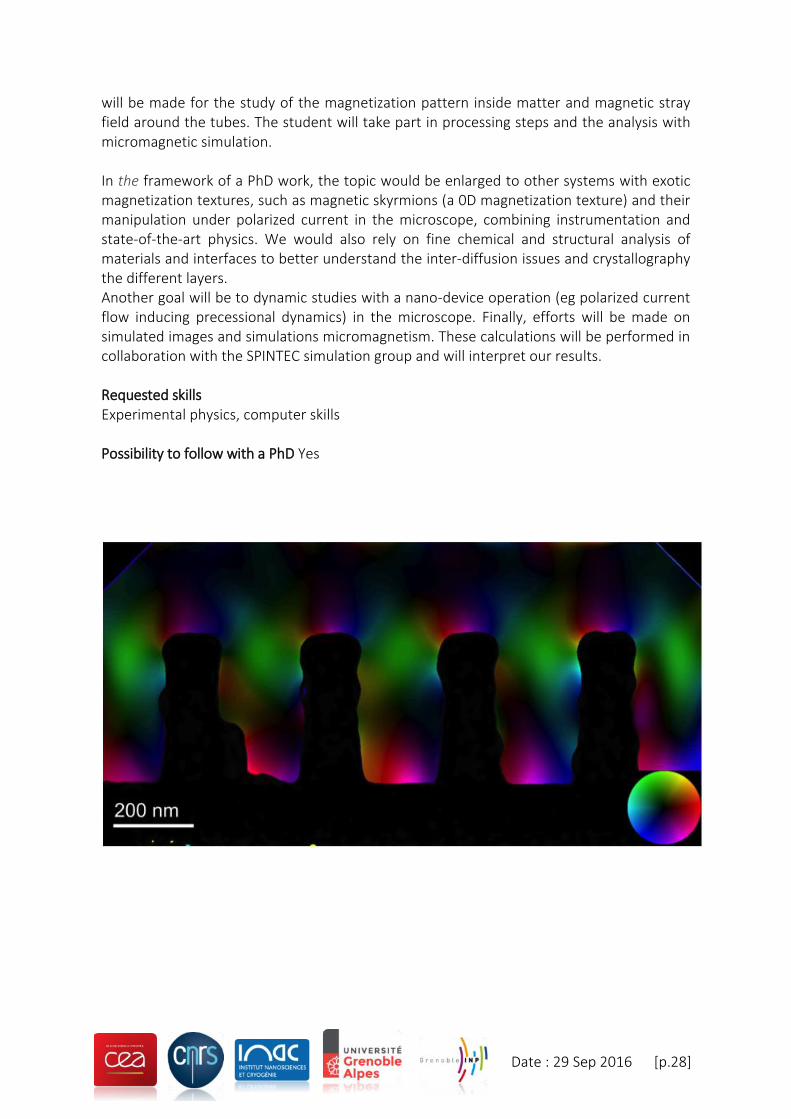
Date : 29 Sep 2016 [p.28]
will be made for the study of the magnetization pattern inside matter and magnetic stray field around the tubes. The student will take part in processing steps and the analysis with micromagnetic simulation. In the framework of a PhD work, the topic would be enlarged to other systems with exotic magnetization textures, such as magnetic skyrmions (a 0D magnetization texture) and their manipulation under polarized current in the microscope, combining instrumentation and state-of-the-art physics. We would also rely on fine chemical and structural analysis of materials and interfaces to better understand the inter-diffusion issues and crystallography the different layers. Another goal will be to dynamic studies with a nano-device operation (eg polarized current flow inducing precessional dynamics) in the microscope. Finally, efforts will be made on simulated images and simulations micromagnetism. These calculations will be performed in collaboration with the SPINTEC simulation group and will interpret our results. Requested skills Experimental physics, computer skills Possibility to follow with a PhD Yes
Date : 29 Sep 2016 [p.29]
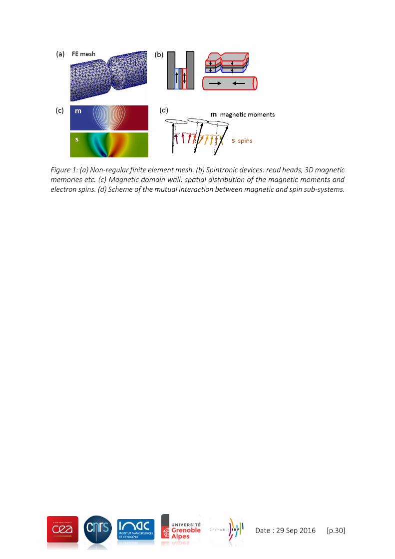
Stage N° : 13 Contact Daria Gusakova ([email protected], tel. +33 4 38 78 65 68) Title FINITE ELEMENT MODELING FOR SPINTRONICS Keywords Spintronics, modeling, finite element methods Summary The interaction between itinerant electron spins and non-trivial magnetic textures such as, for example, magnetic domain walls is of great interest not only for basic research in the field of spintronics but also for storage applications and in the design of logical devices [Fig.1(b)]. Non-trivial geometry of a magnetic structure subjected to spin polarized current may strongly influence its dynamics and the mutual interaction between electron spins and local magnetic moments. Therefore it is important to understand how the different properties of a magnetic system in an experimental framework can be changed through the modification of geometry. This offers new challenges for current spintronics theory and modeling. Details of subject To understand the impact of geometry on spin transport and magnetization dynamics, we have developed the multipurpose micromagnetic finite element c++ software[1,2] jointly in Spintec and Neel Institute. Its non-regular mesh [Fig.1(a)] can accurately describe elliptical cross-section stacks, notched circular shape nanowires, nanocontacts, and other experimental issues. Moreover, in our complex self-consistent approach, the micromagnetic and spin transport equations could be resolved simultaneously [Fig.1(d)]. The purpose of this internship is to study, for example, the magnetic domain wall behavior [Fig.1(c)] under applied current within different geometries. This knowledge is crucial for opening new paths for magnetic memory design. Moreover, this internship is an excellent opportunity to get familiar with the spin dependent transport theories, micromagnetic approach, finite element modeling and various scientific software such as Comsol, MatLab, Origin etc. [1] M. Sturma, J.-C. Toussaint, and D. Gusakova, J. Appl. Phys. 117, 243901 (2015). [2] M. Sturma, C. Bellegarde, J.-C. Toussaint, and D. Gusakova, Phys. Rev. B 94, 104405 (2016). Requested skills condensed matter physics, numerical methods, c++, fluent English or French Possibility to follow with a PhD Yes
Date : 29 Sep 2016 [p.30]
Figure 1: (a) Non-regular finite element mesh. (b) Spintronic devices: read heads, 3D magnetic memories etc. (c) Magnetic domain wall: spatial distribution of the magnetic moments and electron spins. (d) Scheme of the mutual interaction between magnetic and spin sub-systems.