Les lasers à cascade quantique : une technologie des...
62
Les lasers à cascade quantique : une technologie des lasers semiconducteurs pour le MIR et le FIR Université Paris Diderot, Laboratoire Matériaux et Phénomènes Quantiques CNRS, UMR7162, Paris, France. Carlo Sirtori
Transcript of Les lasers à cascade quantique : une technologie des...
Les lasers à cascade quantique :une technologie des lasers
semiconducteurs pour le MIR et le FIR
Université Paris Diderot, Laboratoire Matériaux et Phénomènes QuantiquesCNRS, UMR7162, Paris, France.
Carlo Sirtori
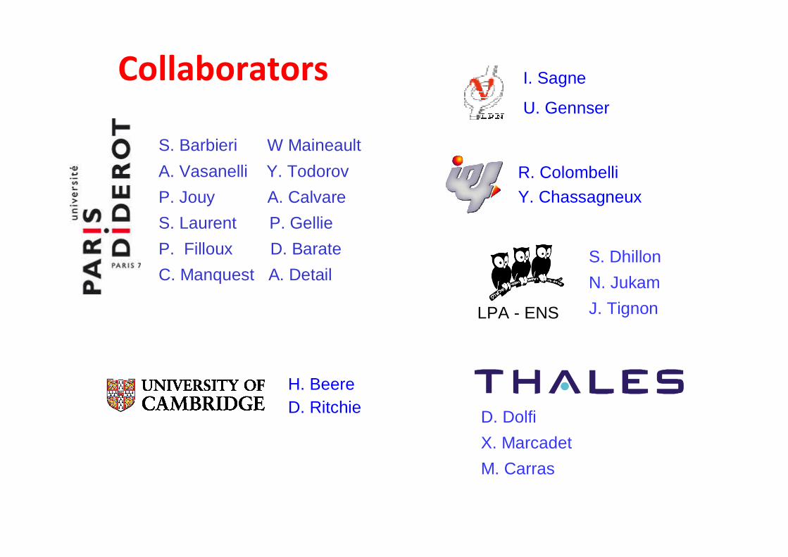
Collaborators
D. Dolfi
X. Marcadet
M. Carras
H. BeereD. Ritchie
R. Colombelli
Y. Chassagneux
I. Sagne
U. Gennser
S. Barbieri W Maineault
A. Vasanelli Y. Todorov
P. Jouy A. Calvare
S. Laurent P. Gellie
P. Filloux D. Barate
C. Manquest A. DetailS. Dhillon
N. Jukam
J. TignonLPA - ENS
Semiconductor lasers
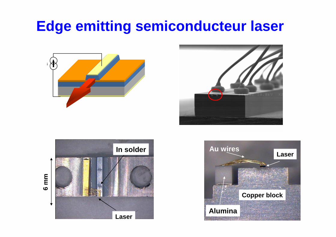
Edge emitting semiconducteur laser
Au wires
Copper block
Laser
6 m
m
Laser
In solder
Alumina
i
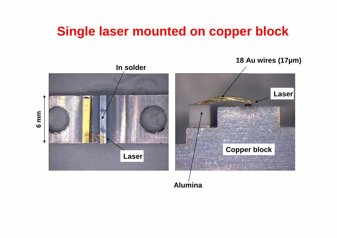
Single laser mounted on copper block
18 Au wires (17µm)In solder
Alumina
6 m
m
LaserCopper block
Laser
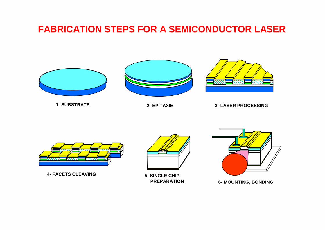
FABRICATION STEPS FOR A SEMICONDUCTOR LASER
1- SUBSTRATE 2- EPITAXIE 3- LASER PROCESSING
4- FACETS CLEAVING 5- SINGLE CHIPPREPARATION 6- MOUNTING, BONDING
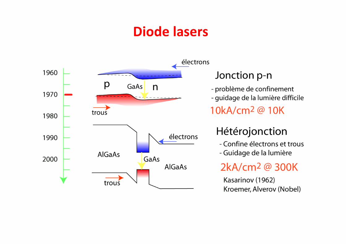
Diode lasers
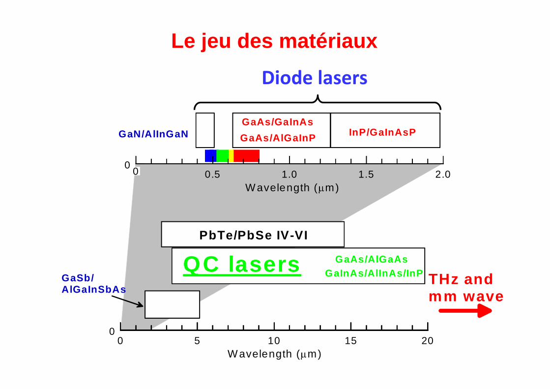
00 5 10 15 20
00.5 1.0 1.5
Wavelength (µm)
Wavelength (µm)
GaAs/GaInAs
GaAs/AlGaInPGaN/AlInGaN InP/GaInAsP
? II-VI compounds ?
GaSb/AlGaInSbAs
QC lasers
0 2.0
GaAs/AlGaAsGaInAs/AlInAs/InP
Diode lasers
THz andmm wave
PbTe/PbSe IV-VI
Le jeu des matériaux
Diode lasers
Quantum Cascade lasers
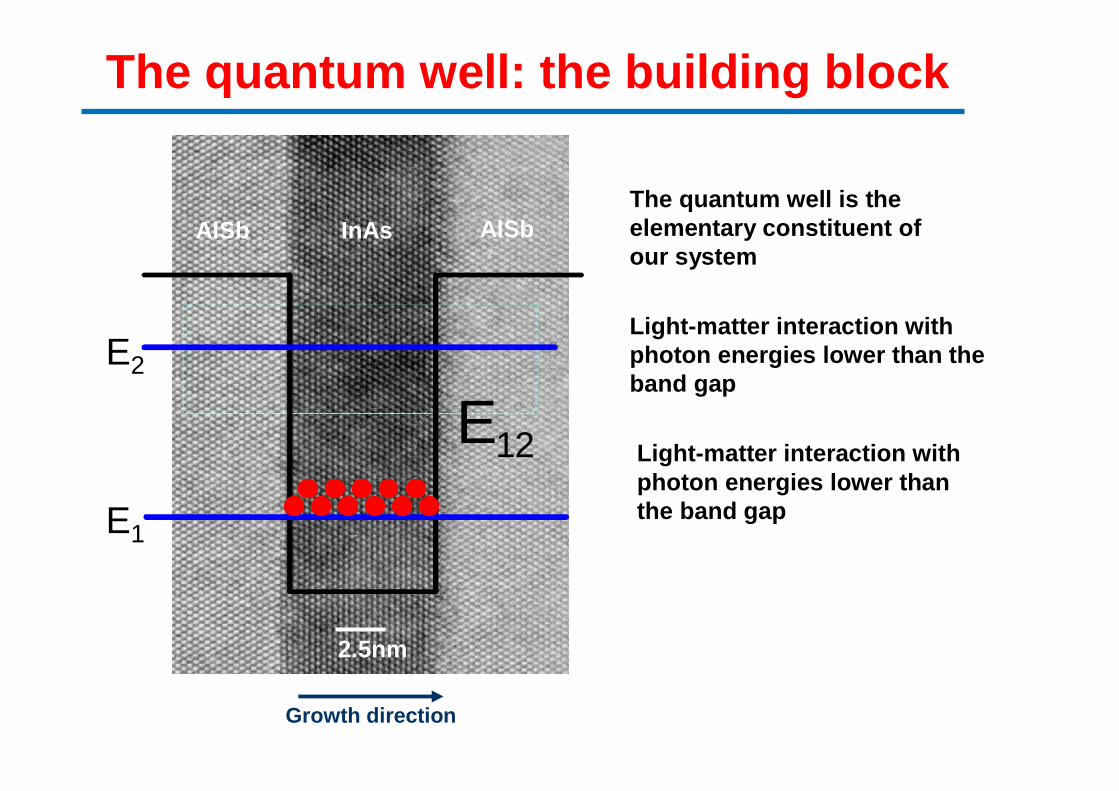
Growth direction
The quantum well: the building block
AlSb AlSbInAs
2.5nm
E12
E1
E2
The quantum well is the elementary constituent of our system
Light-matter interaction with photon energies lower than the band gap
Light-matter interaction with photon energies lower than the band gap
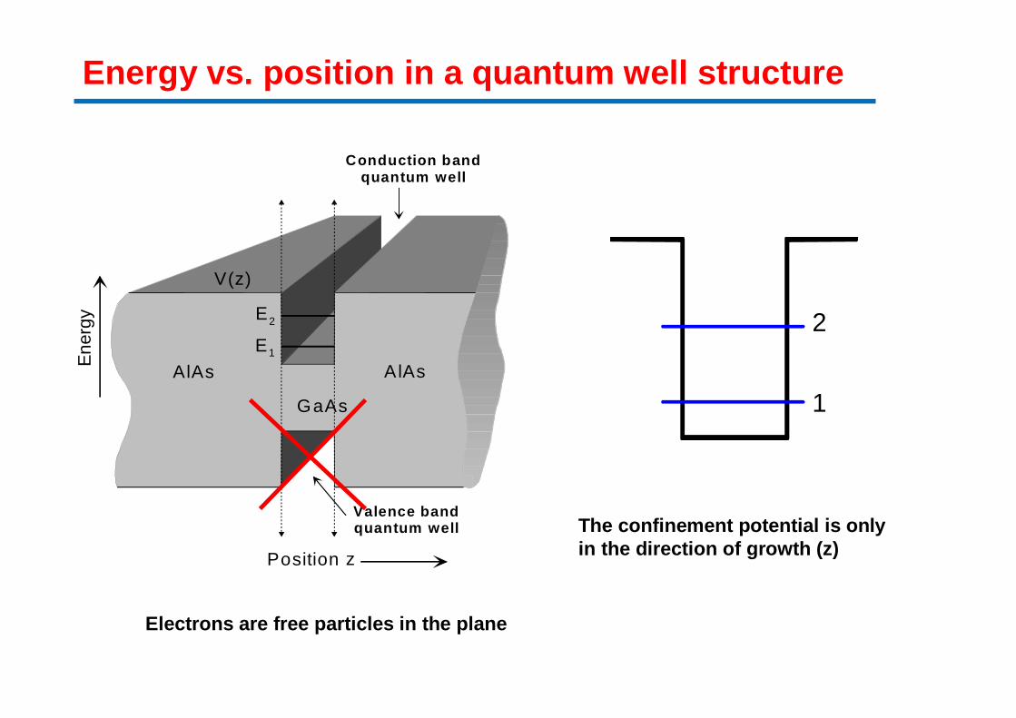
Energy vs. position in a quantum well structure
E1
E2
AlAs
GaAs
AlAs
V(z)
Position z
Ene
rgy
Conduction bandquantum well
Valence bandquantum well
Electrons are free particles in the plane
2
1
The confinement potential is onlyin the direction of growth ( z)
1
2
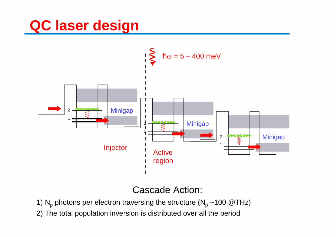
Injection barrier
Minigap
Electron reservoir
QC laser design
1
2 Minigap
1
2 Minigap
Cascade Action:1) Np photons per electron traversing the structure (Np ~100 @THz)
2) The total population inversion is distributed over all the period
1
2 Minigap
Activeregion
Injector
hω = 5 – 400 meV
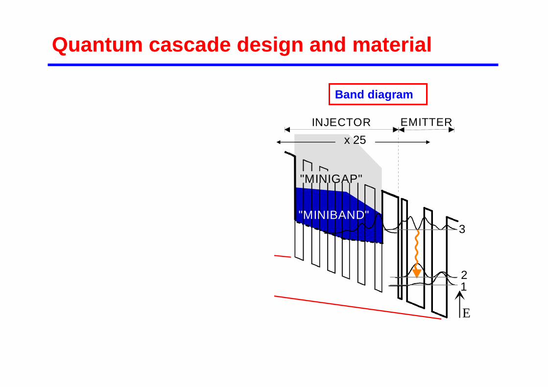
"MINIBAND"
"MINIGAP"
INJECTOR EMITTER
E
x 25
45 n
m
3
21
Band diagramTEM Micrograph
Quantum cascade design and material
Courtesy of C. GmachlBell Labs, Lucent Tech.
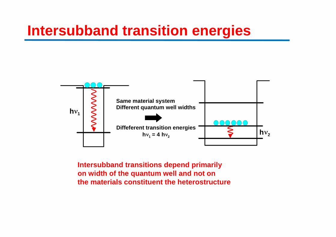
hν1
Same material systemDifferent quantum well widths
Diffeferent transition energieshν1 = 4 hν2
hν2
Intersubband transitions depend primarilyon width of the quantum well and not on the materials constituent the heterostructure
Intersubband transition energies
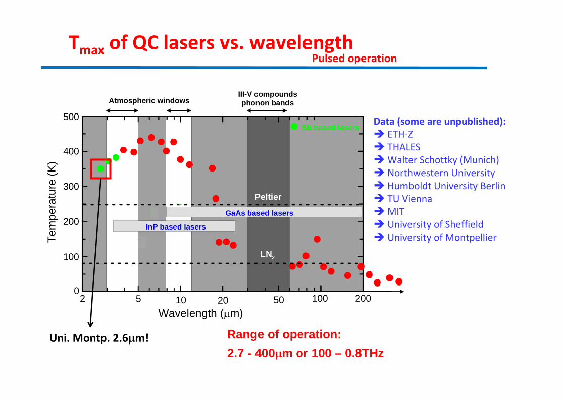
Tmax of QC lasers vs. wavelengthPulsed operation
Data (some are unpublished):� ETH-Z� THALES� Walter Schottky (Munich)� Northwestern University� Humboldt University Berlin� TU Vienna� MIT� University of Sheffield� University of Montpellier
Range of operation:
2.7 - 400µm or 100 – 0.8THz
0
100
200
300
400
2 5 10 20
Tem
pera
ture
(K
)
III-V compoundsphonon bands
LN2
Peltier
Atmospheric windows
500
Wavelength (µm)50 100
GaAs based lasers
InP based lasers
200
Sb based lasers
Uni. Montp. 2.6µm!

Quantum Cascade laserperformances
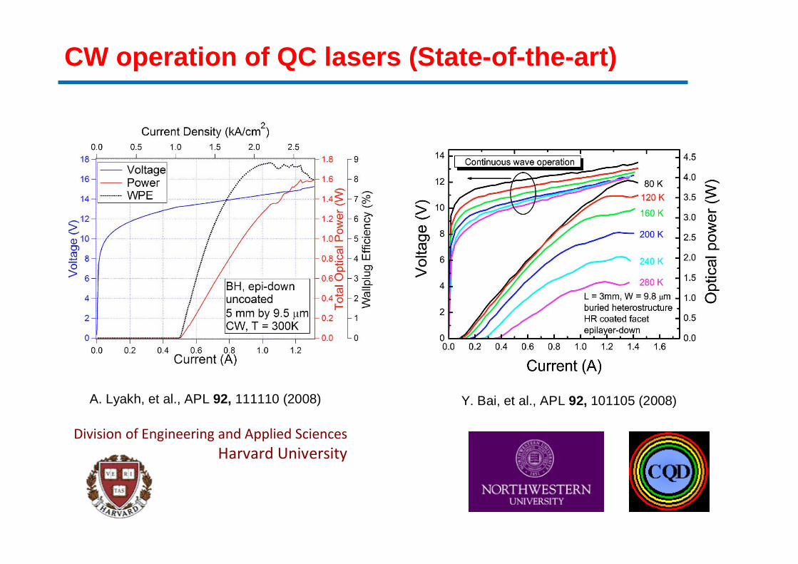
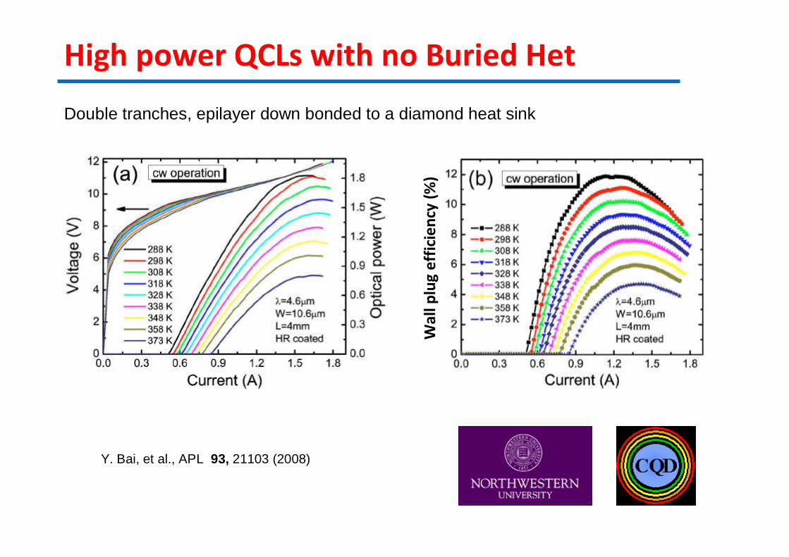
A. Lyakh, et al., APL 92, 111110 (2008) Y. Bai, et al., APL 92, 101105 (2008)
CW operation of QC lasers (State-of-the-art)
Division of Engineering and Applied SciencesHarvard University

Y. Bai, et al., APL 95, 221104 (2009)
Very High power broad area QCLsWide strip lasers are used to increase the volume of the active material
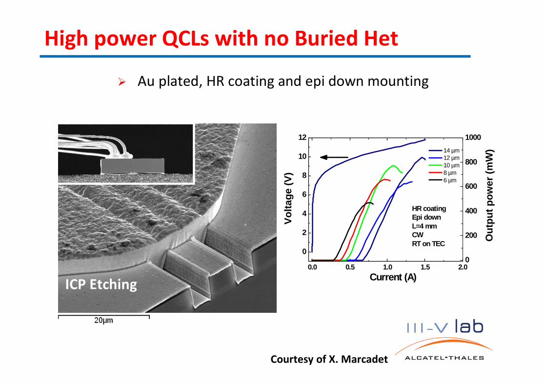
High power QCLs with no Buried Het� Au plated, HR coating and epi down mounting
ICP Etching
Courtesy of X. Marcadet
0.0 0.5 1.0 1.5 2.0
0
2
4
6
8
10
12
Vol
tage
(V
)Current (A)
0
200
400
600
800
1000
HR coatingEpi downL=4 mmCWRT on TEC
14 µm 12 µm 10 µm 8 µm 6 µm
Out
put p
ower
(m
W)
THz lasers
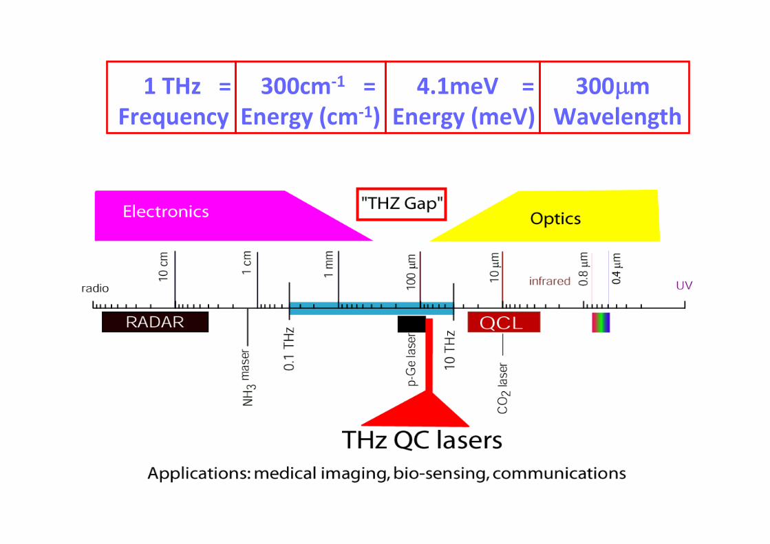
1 THz = 300cm-1 = 4.1meV = 300µmFrequency Energy (cm-1) Energy (meV) Wavelength
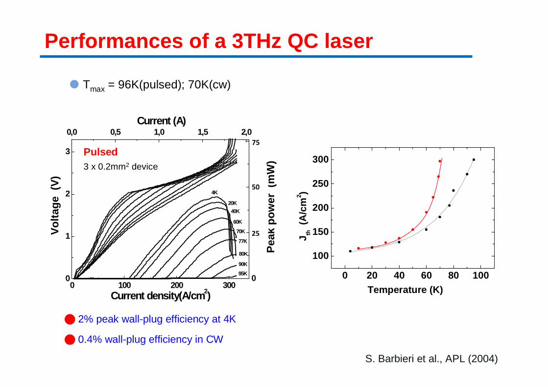
0,0 0,5 1,0 1,5 2,0
0
50
100
150
0 100 200 3000
1
2
3
95K
77K
70K
60K
40K
20K
4K
Pea
k po
wer
(m
W)
Vol
tage
(V
)
Current (A)
90K
80K
Current density(A/cm 2)
Performances of a 3THz QC laser
Pulsed
0 20 40 60 80 100
100
150
200
250
300
J th (
A/c
m2 )
Temperature (K)
� Tmax = 96K(pulsed); 70K(cw)
� 2% peak wall-plug efficiency at 4K
� 0.4% wall-plug efficiency in CW
3 x 0.2mm2 device
S. Barbieri et al., APL (2004)
75
50
25
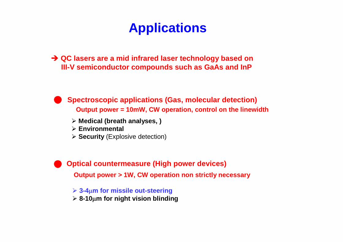
Applications
� QC lasers are a mid infrared laser technology based onIII-V semiconductor compounds such as GaAs and InP
Spectroscopic applications (Gas, molecular detectio n)
Optical countermeasure (High power devices)
� Medical (breath analyses, )� Environmental� Security (Explosive detection)
� 3-4µm for missile out-steering� 8-10µm for night vision blinding
Output power = 10mW, CW operation, control on the l inewidth
Output power > 1W, CW operation non strictly necess ary

1)2)3)4)5)6)7)8)9)
10)11)12)13)14)15)16)17)
List of companies providing QCL wafers, sources and sensor systems
Company name
R.F. Curl et al. Chem. Phys. Lett. 487 (2010) 1–18
Conclusions
� QC lasers are a technology based on III-V semiconductor compounds
� QC cascade lasers ar
� Wavelength can be adjusted by changing the quantum design of the active region rather than its material composition
�QC lasers are unipolar optoelectronic devices (electron only!)
� High performance devices are fabricated :� QC laser operating CW at 300K with Watt level power (λ = 5µm)� QC lasers with tens mW of power in the THz region @ 77K
� QC lasers are the only semiconductor solution in the THz region
�Electrical control of the complex refractive index for frequency and amplitude modulation
� Lasers stabilisation (QC THz stabilised on a frequency comb , NP July)
� Merging QC lasers with other important technologies as: µ-wave, telecom, TDS (femto second).
� Plasmonics and metal guiding
� Very high frequency modulation > 50 GHz
Future
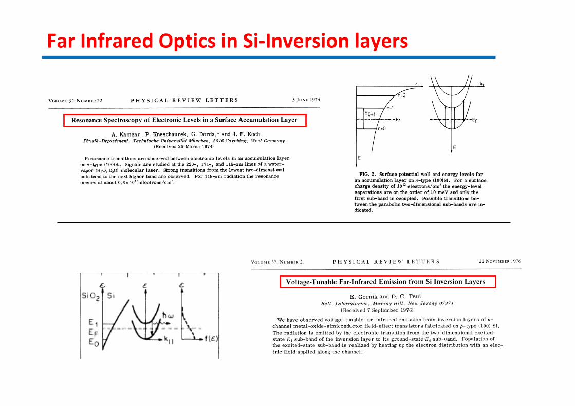
Far Infrared Optics in Si-Inversion layers
EF
K
E
ELO
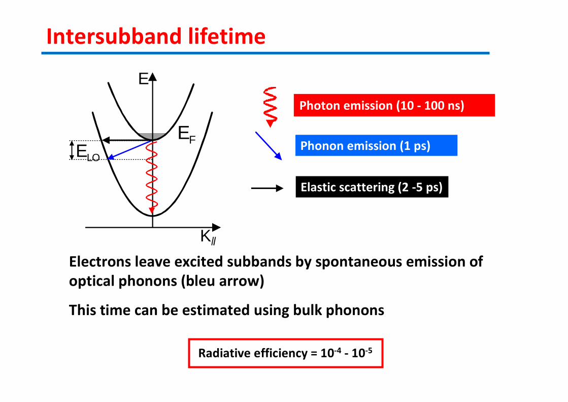
Intersubband lifetime
Photon emission (10 - 100 ns)
Electrons leave excited subbands by spontaneous emission ofoptical phonons (bleu arrow)This time can be estimated using bulk phonons
Radiative efficiency = 10-4 - 10-5
Phonon emission (1 ps)
Elastic scattering (2 -5 ps)
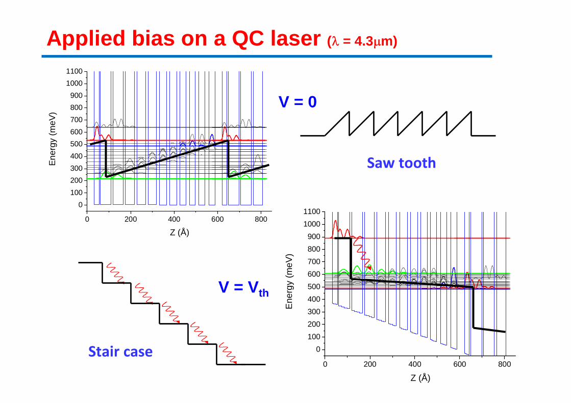
Applied bias on a QC laser (λ = 4.3µm)
0 200 400 600 800
0
100
200
300
400
500
600
700
800
900
1000
1100
Ene
rgy
(meV
)
Z (Å)
V = 0
0 200 400 600 800
0
100
200
300
400
500
600
700
800
900
1000
1100
Ene
rgy
(meV
)
Z (Å)
V = Vth
Saw tooth
Stair case
0
FWHM = 4.6 meV0.10
0.20
100 120 140 160
Photon energy (meV)
Abs
orba
nce
(Log
10T
)
11 10 9 813Wavelength (µm)
T = 10 K Lorenzianline-shape
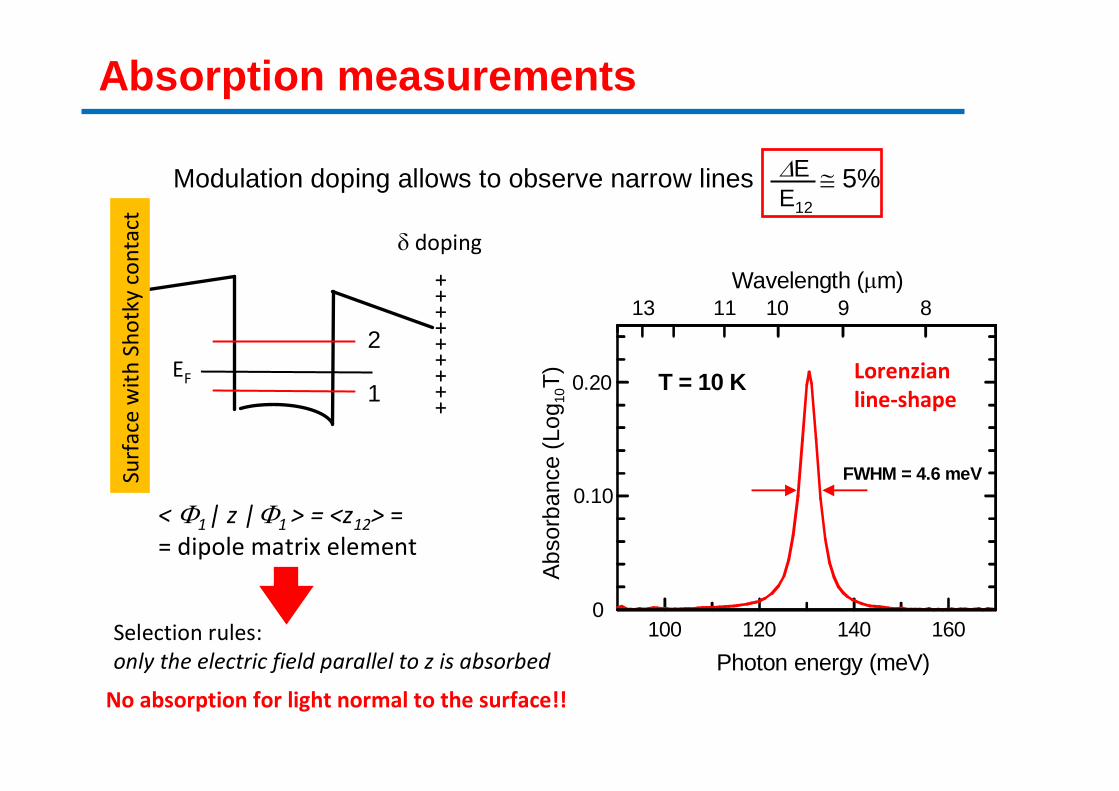
Absorption measurements
1
2
+++++++++
δ doping
EF
Modulation doping allows to observe narrow lines ≅ 5%∆EE12
Surfa
ce w
ith Sh
otky c
ontac
t
< Φ1| z |Φ1 > = <z12> == dipole matrix element
Selection rules:only the electric field parallel to z is absorbed
No absorption for light normal to the surface!!
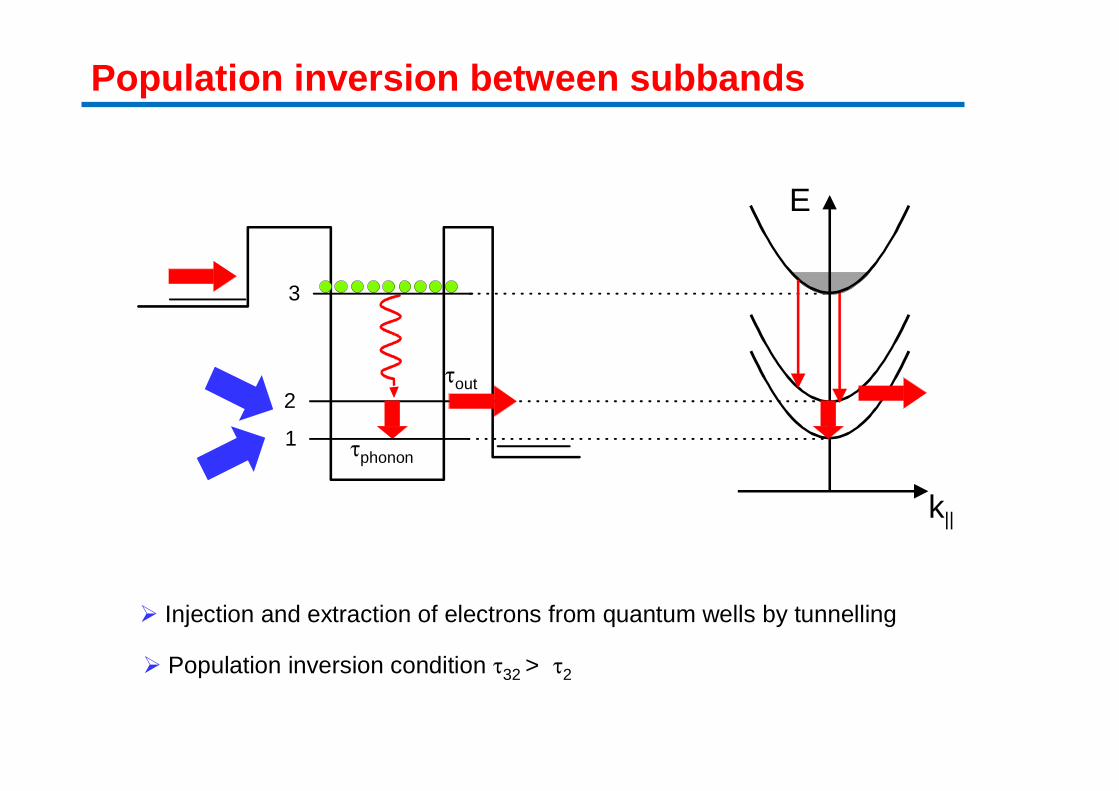
Population inversion between subbands
� Injection and extraction of electrons from quantum wells by tunnelling
1
3
2
E
k||
� Population inversion condition τ32 > τ2
τout
τphonon
k||k||
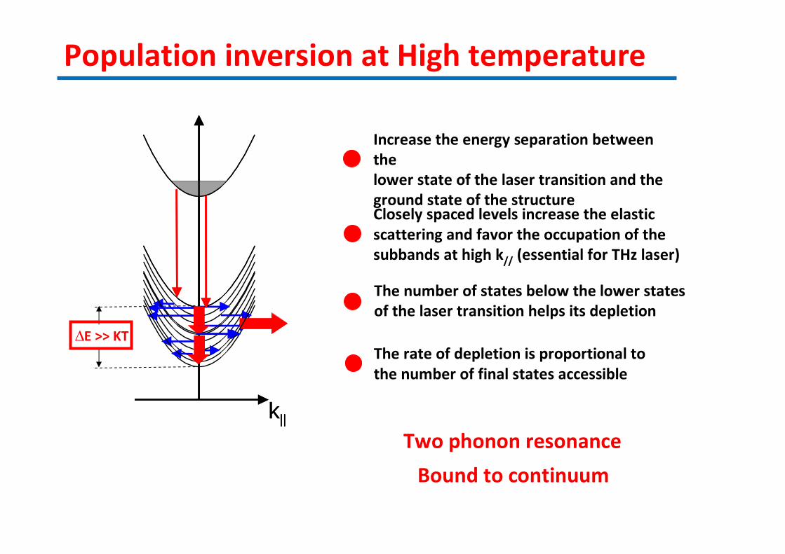
Population inversion at High temperature
The number of states below the lower states of the laser transition helps its depletion
The rate of depletion is proportional to the number of final states accessible
Closely spaced levels increase the elastic scattering and favor the occupation of the subbands at high k// (essential for THz laser)
Two phonon resonanceBound to continuum
∆E >> KT
Increase the energy separation between thelower state of the laser transition and the ground state of the structure
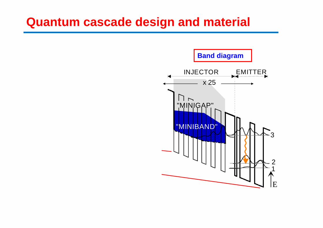
"MINIBAND"
"MINIGAP"
INJECTOR EMITTER
E
x 25
45 n
m
3
21
Band diagramTEM Micrograph
Quantum cascade design and material
Courtesy of C. GmachlBell Labs, Lucent Tech.
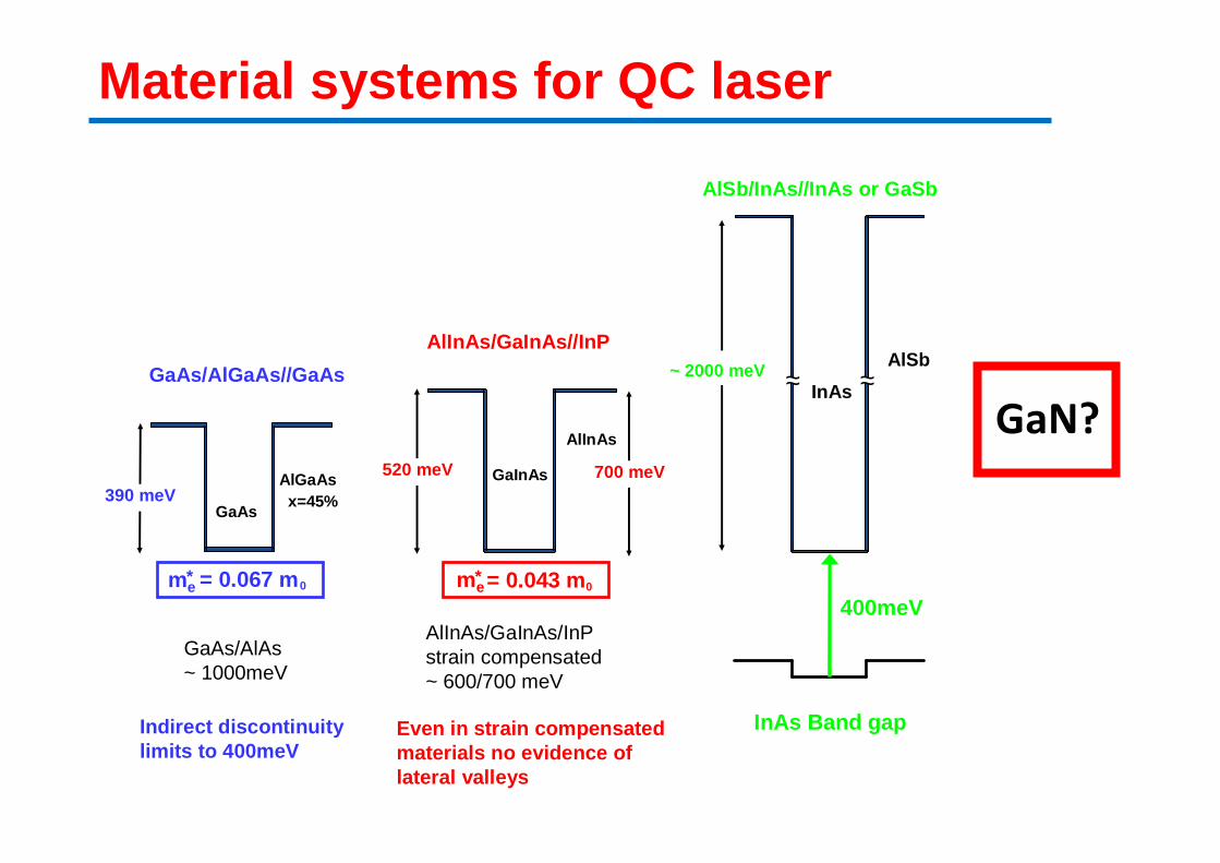
Material systems for QC laser
GaInAs
= 0.043 m0
AlInAs/GaInAs//InP
AlGaAsx=45%
me* = 0.067 m 0
GaAs/AlGaAs//GaAsAlSb
AlInAs
520 meV
~ 2000 meV
GaAs
InAs
AlSb/InAs//InAs or GaSb
= 0.024 m 0
GaAs/AlAs~ 1000meV
AlInAs/GaInAs/InPstrain compensated~ 600/700 meV
~~
390 meV
Indirect discontinuitylimits to 400meV
Even in strain compensatedmaterials no evidence oflateral valleys
Exact position of the lateralminima is unknown
me* me
*
700 meV
InAs is the upper limitat 400meV
~~
400meV
InAs Band gap
GaN?
0
1.5
3.0
4.5
6.0
7.5
9.0
10.5
0 0.1 0.2 0.3 0.4 0.5 0.6 0.7 0.8 0.9
0 0.5 1.0 1.5 2.0 2.5 3.0 3.5 4.0
0
50
100
150
200
250
300
350
400380K
360K
340K
320K
300K
280K
260K
240K
380K
240K
Current [A]
Vol
tage
[V]
Pow
er [m
W]
Threshold current density [kA/cm2]
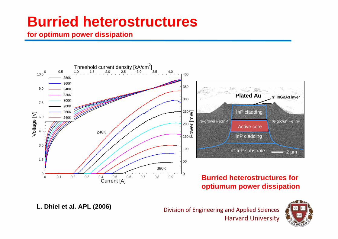
L. Dhiel et al. APL (2006)
Burried heterostructuresfor optimum power dissipation
Burried heterostructures foroptiumum power dissipation
InP cladding
re-grown Fe:InP
InP cladding
n+ InP substrate
re-grown Fe:InP
Plated Au n+ InGaAs layer
2 µm
Active core
Division of Engineering and Applied SciencesHarvard University
Wall
plug
effic
iency
(%)
Y. Bai, et al., APL 93, 21103 (2008)
High power QCLs with no Buried HetDouble tranches, epilayer down bonded to a diamond heat sink
Gain dynamics in QCL
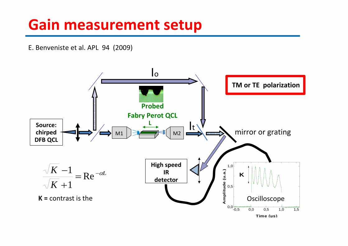
M1 M2
High speed IR
detector
Probed Fabry Perot QCL
Source:chirped DFB QCL
It
TM or TE polarization
K = contrast is the
L
Io
L
K
K α−=+
−Re
1
1
-0,5 0,0 0,5 1,0 1,50,0
0,5
1,0
Am
plitu
de
(u
.a.)
Time (µs)
K
mirror or grating
Gain measurement setupE. Benveniste et al. APL 94 (2009)
Oscilloscope
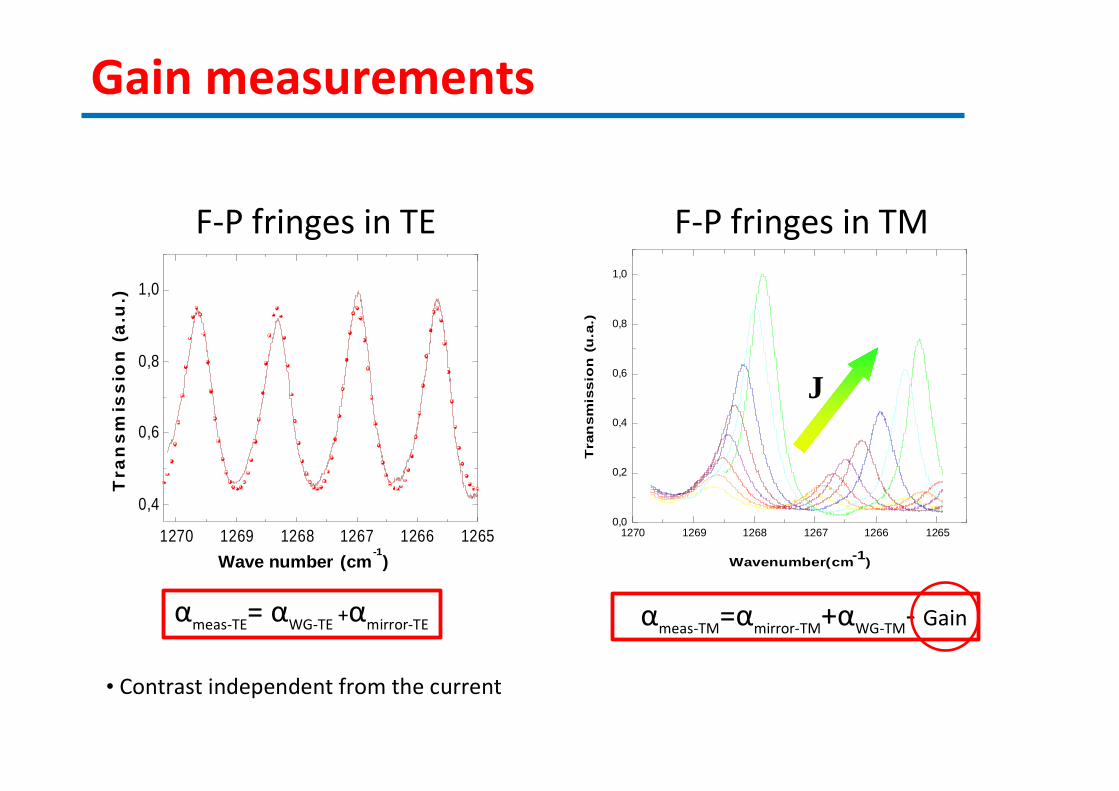
F-P Fringes TE
1270 1269 1268 1267 1266 1265
0,4
0,6
0,8
1,0
Tra
ns
mis
sio
n (
a.u
.)
Wave number (cm-1)
• Contrast independent from the current
αmeas-TE= αWG-TE +αmirror-TE
1270 1269 1268 1267 1266 12650,0
0,2
0,4
0,6
0,8
1,0
Tra
nsm
issio
n (
u.a
.)
Wavenumber (cm -1)
J
αmeas-TM=αmirror-TM+αWG-TM- Gain
F-P fringes in TE F-P fringes in TM
Gain measurements
- 8
- 6
- 4
- 2
0
2
0 0.5 1.0 1.5 0
0.4
0.1
0.2
0.3TE losses
Threshold
Current (A)
Optic
al po
wer (W
)
Gain
(cm-1
)
Gain measurement: intersubband gain and losses
Mirror losses
λ = 5µm
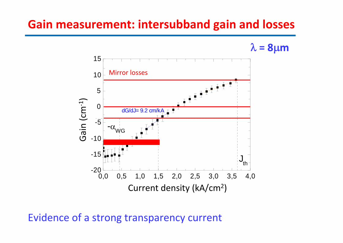
0,0 0,5 1,0 1,5 2,0 2,5 3,0 3,5 4,0-20
-15
-10
-5
0
5
10
15
dG/dJ= 4.1 cm/kA
-αWG
Jth
αM
G-α
ISB
-αW
G (
cm
-1)
J (kA/cm2)
dG/dJ= 9.2 cm/kA
Gain
(cm-1
)
Current density (kA/cm2)
Mirror losses
Gain measurement: intersubband gain and losses
Evidence of a strong transparency current
λ = 8µm

0
5
10
15
0 50 100 150 200
Gain measurement: intersubband gain and lossesλ = 150µm
Measurements performed using a technique first demonstrated in J. Kroll et al Nature (2008)
Gain
(cm-1
)
Current density (kA/cm2)N. Jukam et al. Appl. Phys. Lett (2008)
JthOnset of the gain
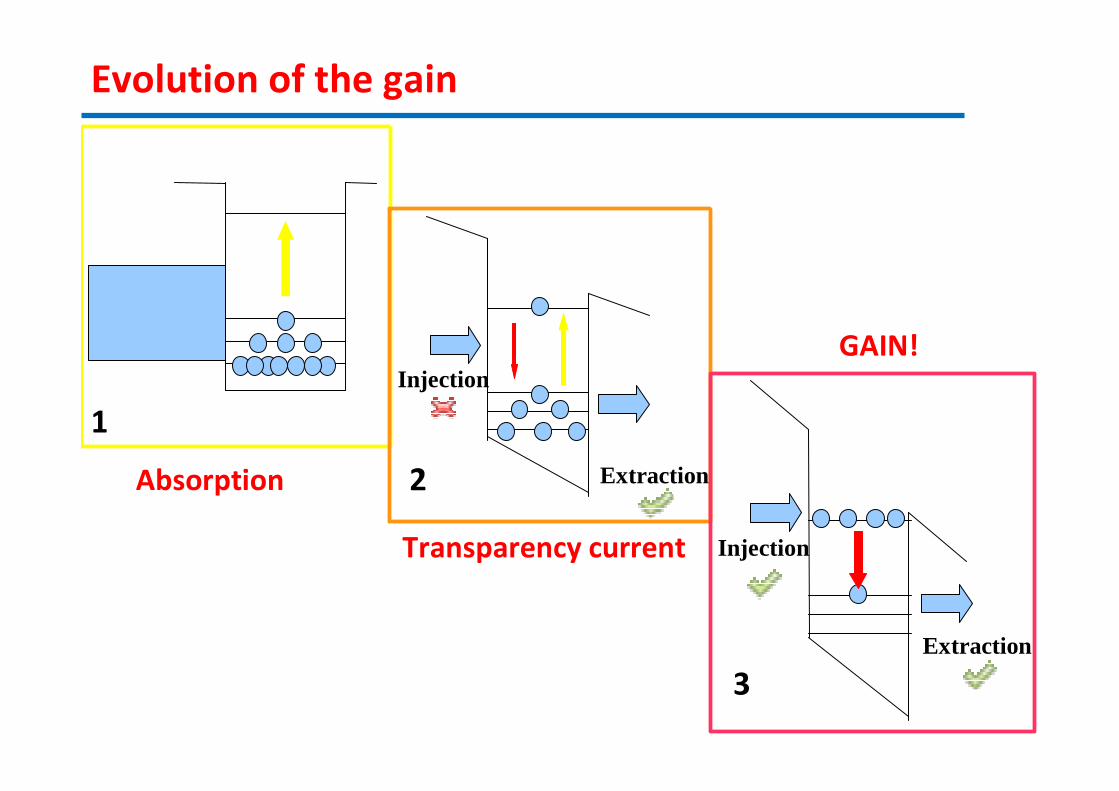
1Injection
Extraction2
Injection
Extraction
3
GAIN!
Transparency currentAbsorption
Evolution of the gain
0 1 2 3 4 5 6 7 8
1
Sig
nal (
u.a.
)
time (µs)
0 1 2 3 4 5 6
300
320
340
360
380
Tem
pera
ture
(K
)
time (µs)
7
8
9
10
Mod
al g
ain
(cm
-1)
320 340 360 380
7,0
7,5
8,0
8,5
9,0
9,5
Mod
al g
ain
(cm
-1)
Temperature (K)
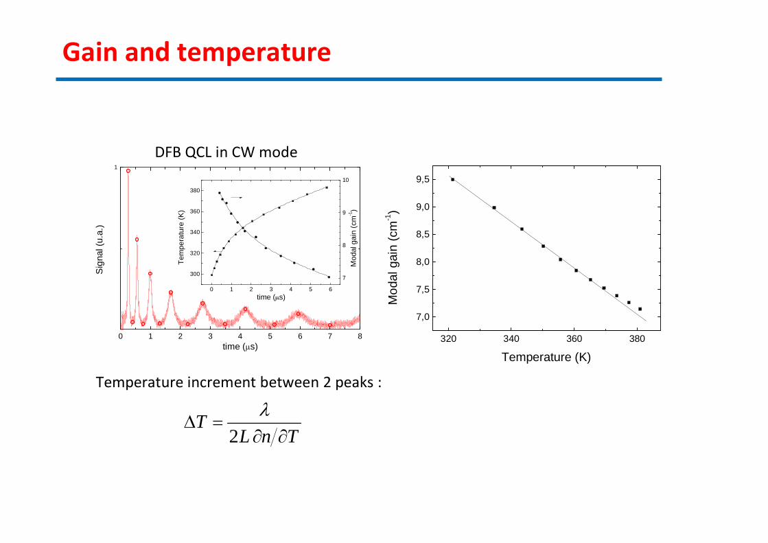
TnLT
∂∂=∆
2
λTemperature increment between 2 peaks :
Gain and temperature
DFB QCL in CW mode

Quantum Cascade laserperformances @ THz frequencies

0,0 0,5 1,0 1,5 2,0
0
50
100
150
0 100 200 3000
1
2
3
95K
77K
70K
60K
40K
20K
4K
Pea
k po
wer
(m
W)
Vol
tage
(V
)
Current (A)
90K
80K
Current density(A/cm 2)
Performances of a 3THz QC laser
Pulsed
0 20 40 60 80 100
100
150
200
250
300
J th (
A/c
m2 )
Temperature (K)
� Tmax = 96K(pulsed); 70K(cw)
� 2% peak wall-plug efficiency at 4K
� 0.4% wall-plug efficiency in CW
3 x 0.2mm2 device
S. Barbieri et al., APL (2004)
75
50
25

THz QCL main challenge: Tmax Operation Balkin et al. APL 2008Tmax = 178K
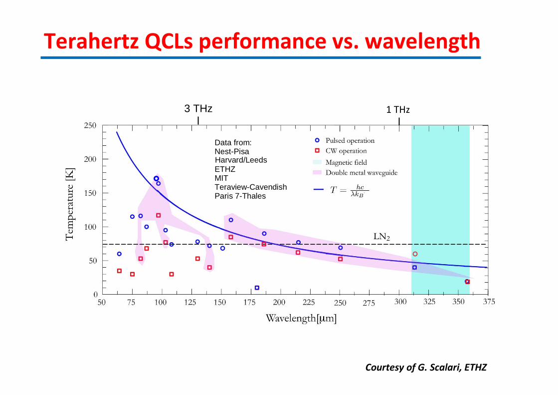
Terahertz QCLs performance vs. wavelength
Data from:Nest-Pisa
ETHZMIT Teraview-CavendishParis 7-Thales
Harvard/Leeds
1 THz3 THz
Courtesy of G. Scalari, ETHZ

Unpilar devices summary and perspectives Quantum cascade lasers are devices based on mature III-V compound semiconductors that have been developed and used for other technologies
Unipolar optoelectronic have imported material, processing and device architecture from the well know III-V platform (diode lasers and detectors). However fundamental physical differences have not yet been fullyexploited:
• Gate contacts and three terminal devices• Parallel transport (acceleration of electron in the quantum well) • Phonon engineering• Extremely short upper state life-time (Ultrafast modulation)• Optical guiding and photonic structures based on metal patterning• Extremely short upper state life-time (Ultrafast modulation)• Optical guiding and photonic structures based on metal patterning
Ultrafast unipolar optoelectronics
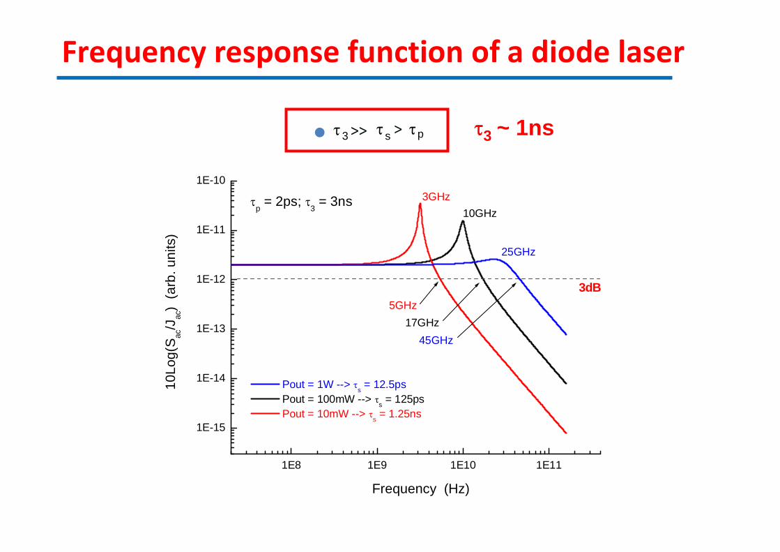
τ3 ~ 1nspττ sτ3 >> >�
1E8 1E9 1E10 1E11
1E-15
1E-14
1E-13
1E-12
1E-11
1E-10
3dB
25GHz
10GHz
3GHz
45GHz
17GHz
5GHz
τp = 2ps; τ
3 = 3ns
10Lo
g(S
ac/J
ac)
(ar
b. u
nits
)
Frequency (Hz)
Pout = 1W --> τs = 12.5ps
Pout = 100mW --> τs = 125ps
Pout = 10mW --> τs = 1.25ns
Frequency response function of a diode laser
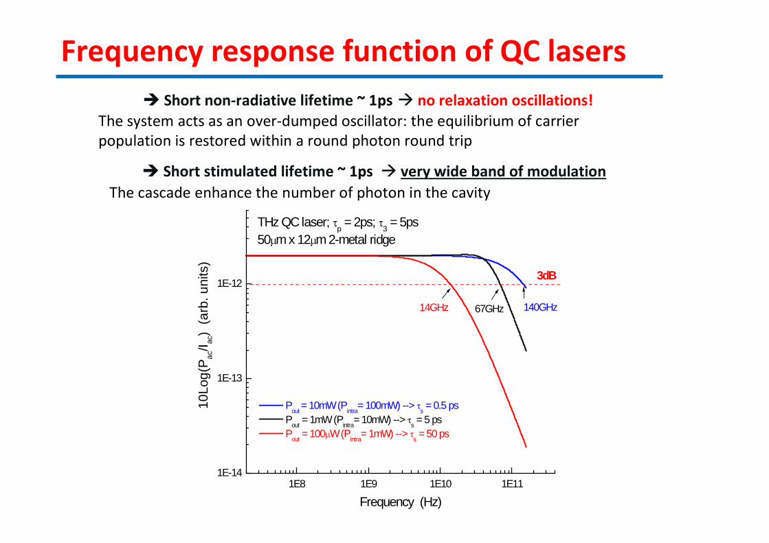
Frequency response function of QC lasers
1E8 1E9 1E10 1E111E-14
1E-13
1E-123dB
Frequency (Hz)
10Lo
g(P
ac/I ac
) (
arb.
uni
ts)
140GHz67GHz14GHz
Pout
= 10mW (Pintra
= 100mW) --> τs = 0.5 ps
Pout
= 1mW (Pintra
= 10mW) --> τs = 5 ps
Pout
= 100µW (Pintra
= 1mW) --> τs = 50 ps
THz QC laser; τp = 2ps; τ
3 = 5ps
50µm x 12µm 2-metal ridge
� Short non-radiative lifetime ~ 1ps� no relaxation oscillations!
� Short stimulated lifetime ~ 1ps � very wide band of modulation
The system acts as an over-dumped oscillator: the equilibrium of carrier population is restored within a round photon round trip
The cascade enhance the number of photon in the cavity

Results on QCLs RF modulationDouble metal QCL; f=2.9THz3mm x 50µm x 12 µm ridge
S. Barbieri et al., Appl. Phys. Lett. 91, 143510 (2007)
R. Paiella et al., Appl. Phys. Lett. 77, 169 (2000)
8.1µm QCL3.75 mm x 4.5 µm ridge with chalcogenide glass insulation layer to reduce devicecapacitance
Double-metal waveguide allow for a low parasitic capacitance without any additional processing �High f modulation limited by wire-bond inductance
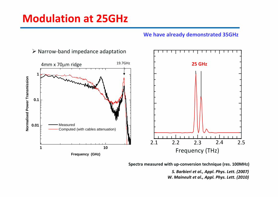
Modulation at 25GHz
� Narrow-band impedance adaptation
1 10
0.01
0.1
1
Measured Computed (with cables attenuation)
Nor
mal
ised
Pow
er T
rans
mis
sion
Frequency (GHz)
4mm x 70µm ridge 19.7GHz
2.20 2.25 2.30 2.35
Frequency (THz)
21.5GHz
20.5GHz20.0GHz
19.5GHz
19.0GHz
18.5GHz
18.0GHz
PRF = 13dBm
Spectra measured with up-conversion technique (res. 100MHz) S. Barbieri et al., Appl. Phys. Lett. (2007)
W. Maineult et al., Appl. Phys. Lett. (2010)
25 GHz
2.1 2.2 2.3 2.4 2.5Frequency (THz)
We have already demonstrated 35GHz
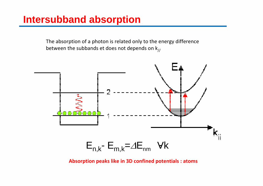
En,k- Em,k=∆Enm Vk
Intersubband absorption
The absorption of a photon is related only to the energy difference between the subbands et does not depends on k//
Absorption peaks like in 3D confined potentials : atoms
Three terminal devices

Three terminal QCL lasers with new functionalities
Vlaser
VControl
Active region
Control Contr
ol cu
rrent
(mA)
Control Voltage (V)
0
0.2
0.4
0.6
-300 -200 -100 0 1000
0.2
0.4
0.6
-300 -200 -100 0 100
V1 =0 V1 ∼2V
8µm 10µm
0 200.00
0.02
0.04
0.06
0.08
0.10
Γ = 100%α = 13 cm-1
met
al la
yer
met
al la
yer
activ
e re
gion
Mod
e in
tens
ity (
arb.
uni
ts)
Distance ( µm)
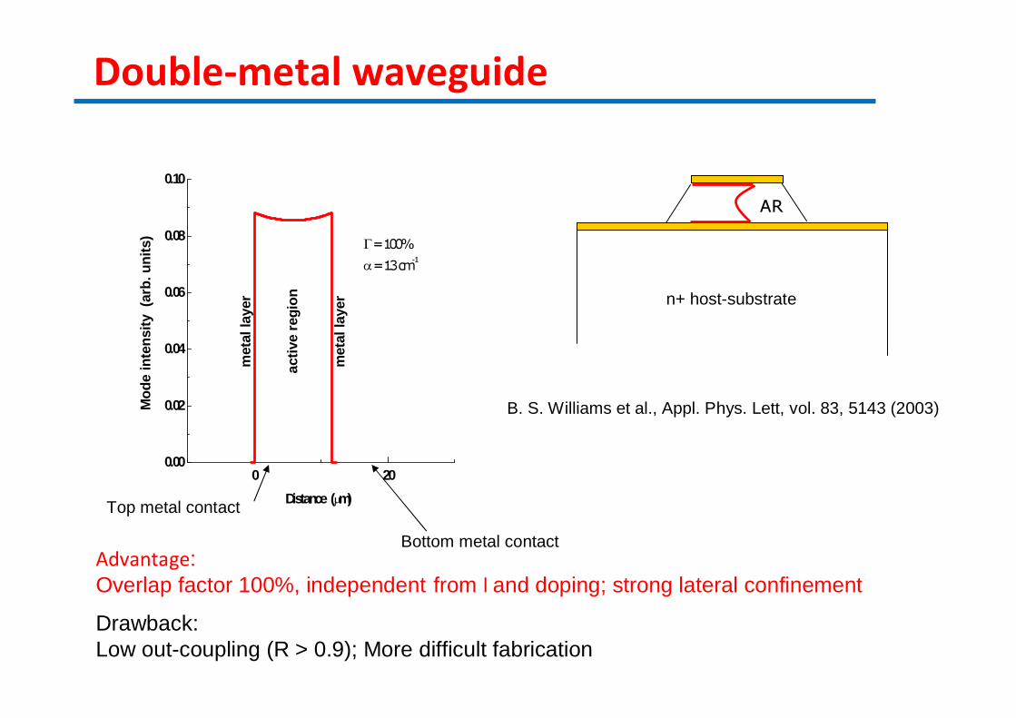
Double-metal waveguide
Advantage: Overlap factor 100%, independent from l and doping; strong lateral confinement
Drawback:Low out-coupling (R > 0.9); More difficult fabrication
AR
Top metal contact
Bottom metal contact
B. S. Williams et al., Appl. Phys. Lett, vol. 83, 5143 (2003)
n+ host-substrate

Far field of a metal-metal QC THz laser
y
x
12mm
52mm
mode intensityprofile
The strong interaction between the guided mode and the metal excite the top contact which act as an antenna
Metal-metal devices
z
y
x
fqsubstrate
-20 0 20 40 60 80
-20
0
-40
20
40
(b)�
Lase
r T
op
Data
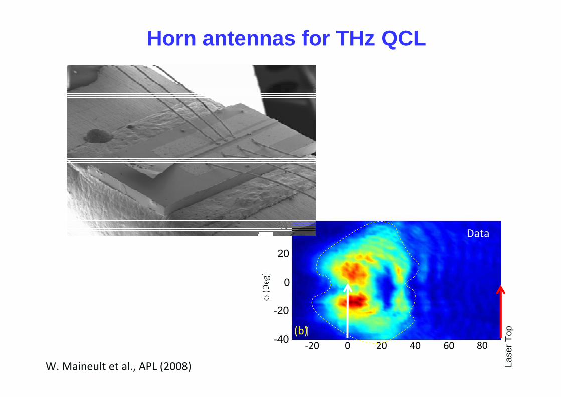
Horn antennas for THz QCL
W. Maineult et al., APL (2008)

Exploiting the extreme optical confinement
h
Double metal
A.R.
Metal AR air
Mismatch between the DM mode and Metal-AR-air modeIndex contrast
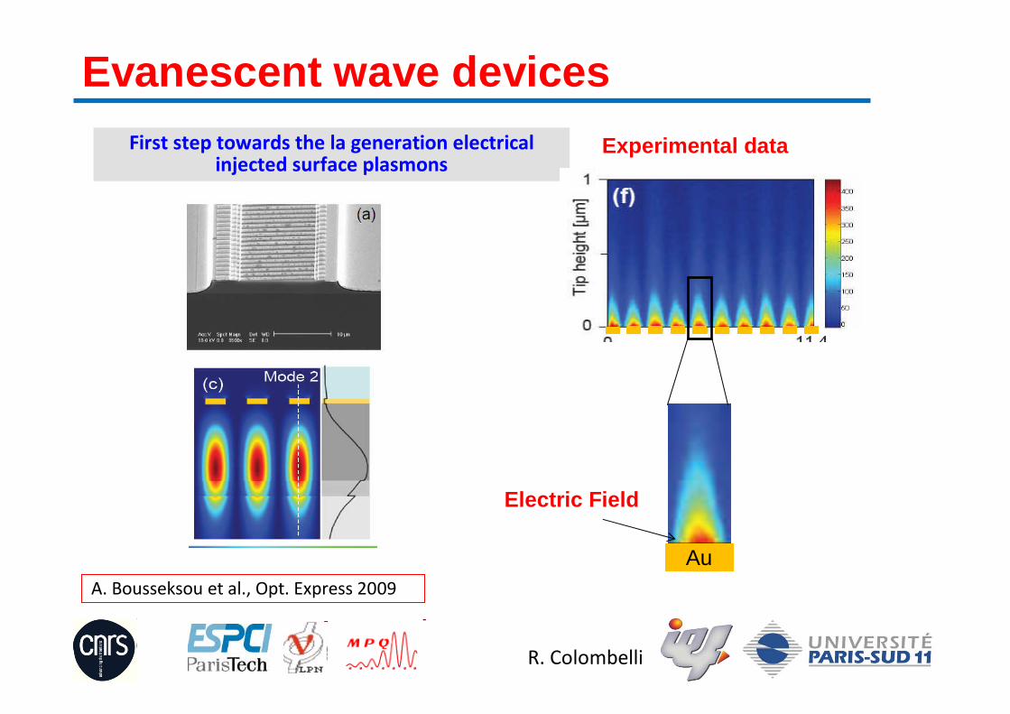
A. Bousseksou et al., Opt. Express 2009
First step towards the la generation electrical injected surface plasmons Experimental data
Au
Electric Field
Evanescent wave devices
R. Colombelli