
Juha Jokipii Dynamic Characteristics of Grid-Connected ...
114
Juha Jokipii Dynamic Characteristics of Grid-Connected Three-Phase Z-Source Inverter in Photovoltaic Applications Julkaisu 1377 • Publication 1377 Tampere 2016
Transcript of Juha Jokipii Dynamic Characteristics of Grid-Connected ...

Juha JokipiiDynamic Characteristics of Grid-Connected Three-Phase Z-Source Inverter in Photovoltaic Applications
Julkaisu 1377 • Publication 1377
Tampere 2016
Tampereen teknillinen yliopisto. Julkaisu 1377 Tampere University of Technology. Publication 1377
Juha Jokipii
Dynamic Characteristics of Grid-Connected Three-Phase Z-Source Inverter in Photovoltaic Applications Thesis for the degree of Doctor of Science in Technology to be presented with due permission for public examination and criticism in Festia Building, Auditorium Pieni Sali 1, at Tampere University of Technology, on the 15th of April 2016, at 12 noon.
Tampereen teknillinen yliopisto - Tampere University of Technology Tampere 2016

ISBN 978-952-15-3720-2 (printed) ISBN 978-952-15-3728-8 (PDF) ISSN 1459-2045
ABSTRACT
Due to the inevitable depletion of fossil fuels and increased awareness of their harmful environ-
mental effects, the world energy sector has been moving towards extensive use of renewable
energy resources, such as solar energy. In solar photovoltaic power generation, the needed
interface between the source of electrical energy, i.e., a photovoltaic generator, and electri-
cal energy transmission and distribution systems is provided by power electronic converters
known as inverters. One of the latest addition into the large group of inverter topologies is
a Z-source inverter (ZSI), whose suitability for different applications have been extensively
studied since its introduction in 2002. This thesis addresses the dynamic characteristics of
a three-phase grid-connected Z-source inverter when applied to interfacing of photovoltaic
generators. Photovoltaic generators have been shown to affect the behavior of the interfacing
power converters but these issues have not been studied in detail thus far in case of ZSI.
In this thesis, a consistent method for modeling a three-phase grid-connected photovoltaic
ZSI was developed by deriving an accurate small-signal model, which was verified by simula-
tions and experimental measurements by means of a small-scale laboratory prototype inverter.
According to the results presented in this thesis, the small-signal characteristics of a photo-
voltaic generator-fed and a conventional voltage-fed ZSI differs from each other.
The derived small-signal model was used to develop deterministic procedure to design the
control system of the inverter. It is concluded that a feedback loop that adjusts the shoot-
through duty cycle should be used to regulate the input voltage of the inverter. Under input
voltage control, there is no tradeoff in between the parameters of the impedance network
and impedance network capacitor voltage control bandwidth. Also the small mismatch in the
impedance network parameters do not compromise the performance of the inverter. These
phenomena will remain hidden if the effect of the photovoltaic generator is not taken into
account. In addition, the dynamic properties of the ZSI-based PV inverter was compared to
single and two-stage VSI-based inverters. It is shown that the output impedance of ZSI-based
inverter is similar to VSI-based inverter if the input voltage control is designed according to
method presented in the thesis. In addition, it is shown that the settling time of the system,
which determines the maximum power point tracking performance, is similar to two-stage
VSI-based inverter.
The control of the ZSI-based PV inverter is more complicated than the control of the VSI-
based inverter. However, with the model presented in this thesis, it is possible to guarantee
that the performance of the inverter resembles the behavior of the two-stage VSI, i.e. the use
of ZSI in interfacing of photovoltaic generators is not limited by its dynamic properties.
iii

PREFACE
The work was carried out at the Department of Electrical Energy at Tampere University of
Technology (TUT) during the years 2012 - 2015. The research was funded by TUT, Doctoral
Programme in Electrical Energy Engineering, and ABB Oy. I’m grateful for the personal
grants from Finnish Foundation for Technology Promotion, Ulla Tuominen Foundation, and
Walter Ahlstrom Foundation.
First of all, I would like to express my deepest gratitude to Professor Teuvo Suntio for
supervising my thesis. I want to thank you for having trust in me, and providing enlightening
guidance and inspiring instructions during my academic career. Secondly, I want to thank
my colleagues, PhD Tuomas Messo, PhD Jenni Rekola, M.Sc Jukka Viinamaki, M.Sc Aapo
Aapro, M.Sc Jyri Kivimaki, and M.Sc Kari Lappalainen for their help in professional matters
and providing excellent working atmosphere. It has been a pleasure to work in a research
group consisting of highly motivated and inspiring people. Additionally, I want to thank my
former colleagues PhD Joonas Puukko, PhD Juha Huusari, PhD Lari Nousiainen, PhD Anssi
Maki, PhD Diego Torres Lobera, M.Sc Antti Virtanen, and M.Sc Anssi Makinen for their help
and guidance in the beginning of my PhD studies. Moreover, I wish to express my gratitude
to the pre-examiners Professor Frede Blaabjerg and Associate Professor Pedro Roncero for
their valuable comments and suggestions regarding the thesis manuscript, laboratory engineers
Pentti Kivinen and Pekka Nousiainen for their assistance in the laboratory experiments, and
Merja Teimonen, Terhi Salminen, Nitta Laitinen and Mirva Seppanen for organizing everyday
matters in the department.
Finally, and most importantly, I want to thank my wife Anni, parents Hannu and Raija,
my brother Tuomo, and sister Katariina for believing in me and providing unfailing support
and encouragement during my academic career.
Tampere, January 2016
Juha Jokipii
iv

CONTENTS
Abstract iii
Preface iv
Table of contents v
Symbols and abbreviations vii
1 Introduction 1
1.1 Role of power electronics in energy production . . . . . . . . . . . . . . . . . . 1
1.2 Overview of solar photovoltaic power systems . . . . . . . . . . . . . . . . . . . 2
1.3 Z-source inverter (ZSI) . . . . . . . . . . . . . . . . . . . . . . . . . . . . . . . . 7
1.4 Motivation of the thesis . . . . . . . . . . . . . . . . . . . . . . . . . . . . . . . 9
1.5 Scientific contribution . . . . . . . . . . . . . . . . . . . . . . . . . . . . . . . . 10
1.6 Structure of the thesis . . . . . . . . . . . . . . . . . . . . . . . . . . . . . . . . 11
2 Dynamic characterization of voltage-source inverters 13
2.1 On small-signal modeling of interfacing power electronic converters . . . . . . . 13
2.2 Voltage-fed VSI-based grid-connected inverter . . . . . . . . . . . . . . . . . . . 17
2.2.1 Open-loop characteristics . . . . . . . . . . . . . . . . . . . . . . . . . . 17
2.2.2 Closed-loop characteristics . . . . . . . . . . . . . . . . . . . . . . . . . . 21
2.2.3 The effect of non-ideal source on dynamics of VSI-based inverter . . . . 25
2.3 VSI-based single and two-stage photovoltaic inverters . . . . . . . . . . . . . . . 27
2.3.1 Single-stage VSI-based photovoltaic inverter . . . . . . . . . . . . . . . . 27
2.3.2 Two-stage VSI-based photovoltaic inverter . . . . . . . . . . . . . . . . . 30
2.4 Conclusions . . . . . . . . . . . . . . . . . . . . . . . . . . . . . . . . . . . . . . 32
3 Dynamic characterization of Z-source inverters 33
3.1 Modeling of a voltage-fed and current-fed Z-source inverters . . . . . . . . . . . 33
3.1.1 Modeling of a voltage-fed Z-source inverter impedance network . . . . . 34
3.1.2 Modeling of a current-fed Z-source inverter impedance network . . . . . 41
3.1.3 Comparison of current-fed and voltage-fed ZSI dynamic characteristics . 47
3.2 Modeling of a photovoltaic Z-source inverter . . . . . . . . . . . . . . . . . . . . 53
3.3 Experimental evidence . . . . . . . . . . . . . . . . . . . . . . . . . . . . . . . . 56
v

3.4 Conclusions . . . . . . . . . . . . . . . . . . . . . . . . . . . . . . . . . . . . . . 58
4 Issues on modeling and control of photovoltaic Z-source inverter 59
4.1 Impedance network capacitor voltage control . . . . . . . . . . . . . . . . . . . 59
4.2 Determining the value of minimum impedance network capacitance . . . . . . . 66
4.3 Effect of control-mode on control system performance . . . . . . . . . . . . . . 67
4.4 Effect of asymmetric impedance network on control system performance . . . . 70
4.5 Experimental evidence . . . . . . . . . . . . . . . . . . . . . . . . . . . . . . . . 72
4.6 Conclusions . . . . . . . . . . . . . . . . . . . . . . . . . . . . . . . . . . . . . . 74
5 Comparison of dynamic characteristics of VSI and ZSI-based PV inverters 77
5.1 Appearance of RHP zero in dynamics . . . . . . . . . . . . . . . . . . . . . . . 77
5.2 Output impedance . . . . . . . . . . . . . . . . . . . . . . . . . . . . . . . . . . 78
5.3 Input voltage control . . . . . . . . . . . . . . . . . . . . . . . . . . . . . . . . . 80
5.4 Conclusions . . . . . . . . . . . . . . . . . . . . . . . . . . . . . . . . . . . . . . 82
6 Conclusions 83
6.1 Final conclusions . . . . . . . . . . . . . . . . . . . . . . . . . . . . . . . . . . . 83
6.2 Future topics . . . . . . . . . . . . . . . . . . . . . . . . . . . . . . . . . . . . . 84
References 85
Appendices 93
A Alpha-beta and direct-quadrature -frames 93
B Transfer functions of a voltage-fed VSI-based inverter 95
C Transfer functions of a two-stage inverter voltage-boosting stage 97
D Laboratory setup 100
vi

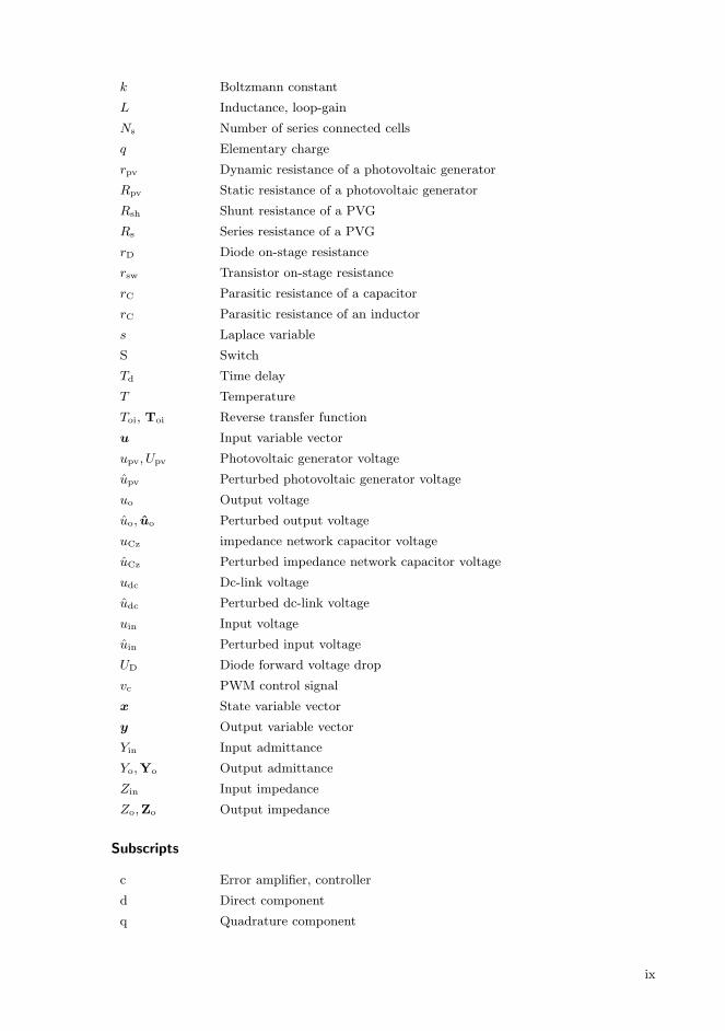
SYMBOLS AND ABBREVIATIONS
Abbreviations
AC, ac Alternating current
AD Analog-to-digital conversion
CC, cf Constant-current
CF, cf Current-fed
CSI Current-source inverter
CV, cf Constant-voltage
CCM Continuous conduction mode
DA Digital-to-analog conversion
dB Decibel
dc Direct current
DSP Digital signal processor
ESR Equivalent series resistance
FPGA Field-gate-programmable array
IGBT Insulated gate bipolar junction transistor
LHP Left half plane
NPC Neutral-point clamped
MPP Maximum power point
MPPT Maximum power point tracking
OC Open-circuit
PI Proportional-integral controller
PLL Phase-locked loop
PV Photovoltaic
PVG Photovoltaic generator
PWM Pulse-width modulation
RHP Right half plane
SC Short-circuit
STC Standard-test conditions
VF, vf Voltage-fed
VSI Voltage-source inverter
ZSI Z-source inverter
vii

Greek characters
α Alpha-component in stationary reference frame
β Beta-component in stationary reference frame
∆ Determinant, difference
ω Angular frequency
θ Vector angle
Φ State-transition matrix
Latin characters
a Diode ideality factor
A Coefficient matrix of the state-space representation
B Coefficient matrix of the state-space representation
B Boost factor
C Coefficient matrix of the state-space representation
c Control variable
C1, C2 Impedance network capacitance
Cin Input capacitor impedance
Cdc Dc-link capacitance
d Differential operator
D, d Duty ratio
D′, d′ Complement of the duty ratio
D Coefficient matrix of the state-space representation
f Frequency
G Transfer function matrix
Gci, Gci Control-to-input transfer function
Gco, Gco Control-to-output transfer function
GcZc Control-to-impedance network capacitor voltage transfer function
Gio, Gio Forward transfer function
GiZc Input-to-impedance network capacitor voltage transfer function
GoZc Output-to-impedance network capacitor voltage transfer function
I Identity matrix
ipv, Ipv Photovoltaic generator current
iph, Iph Photocurrent
id, Id Diode current
iin Input current
iin Perturbed input current
io Output current
io, io Perturbed output current
idc Dc-link current
idc Perturbed dc-link current
I0 Diode reverse saturation current
viii
k Boltzmann constant
L Inductance, loop-gain
Ns Number of series connected cells
q Elementary charge
rpv Dynamic resistance of a photovoltaic generator
Rpv Static resistance of a photovoltaic generator
Rsh Shunt resistance of a PVG
Rs Series resistance of a PVG
rD Diode on-stage resistance
rsw Transistor on-stage resistance
rC Parasitic resistance of a capacitor
rC Parasitic resistance of an inductor
s Laplace variable
S Switch
Td Time delay
T Temperature
Toi, Toi Reverse transfer function
u Input variable vector
upv, Upv Photovoltaic generator voltage
upv Perturbed photovoltaic generator voltage
uo Output voltage
uo, uo Perturbed output voltage
uCz impedance network capacitor voltage
uCz Perturbed impedance network capacitor voltage
udc Dc-link voltage
udc Perturbed dc-link voltage
uin Input voltage
uin Perturbed input voltage
UD Diode forward voltage drop
vc PWM control signal
x State variable vector
y Output variable vector
Yin Input admittance
Yo,Yo Output admittance
Zin Input impedance
Zo,Zo Output impedance
Subscripts
c Error amplifier, controller
d Direct component
q Quadrature component
ix

lf low-frequency
st shoot-through
conv Refers to the control system reference frame
grid Refers to the synchronous reference frame
inf Refers to ideal transfer function
Superscripts
cf-in Refers to transfer functions of current-fed impedance network
vf-in Refers to transfer functions of voltage-fed impedance network
in Refers to transfer functions of an input voltage-controlled converter
T Transpose
out Refers to transfer functions of an output current-controlled converter
S Refers to source affected transfer functions
vsi Refers to transfer functions of VSI
zsi Refers to transfer functions of ZSI
x
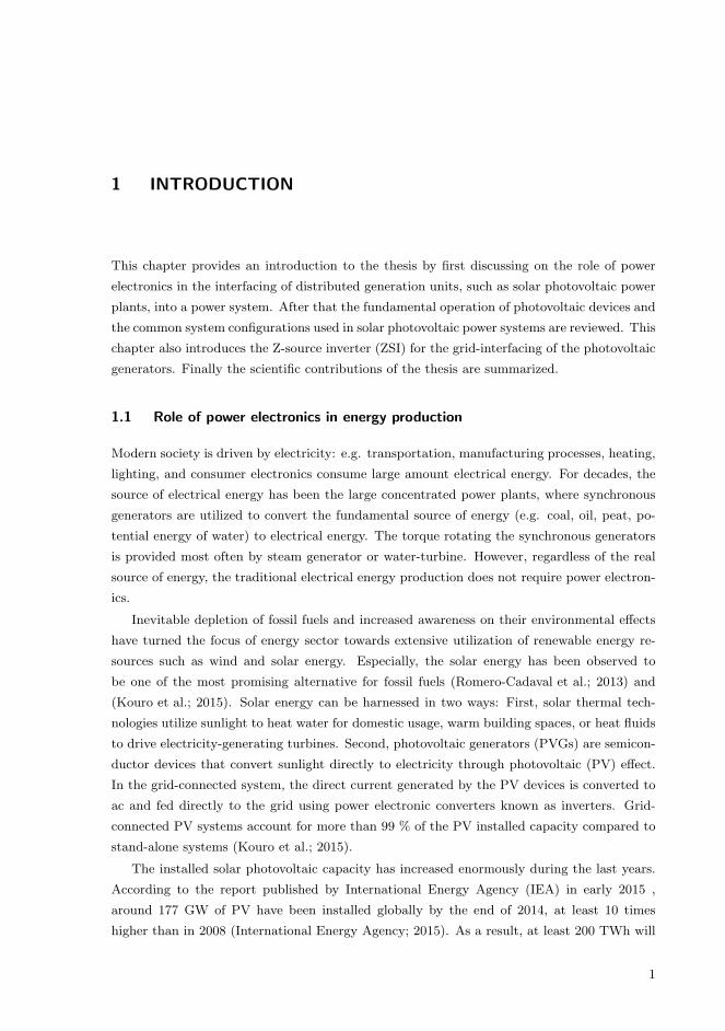
1 INTRODUCTION
This chapter provides an introduction to the thesis by first discussing on the role of power
electronics in the interfacing of distributed generation units, such as solar photovoltaic power
plants, into a power system. After that the fundamental operation of photovoltaic devices and
the common system configurations used in solar photovoltaic power systems are reviewed. This
chapter also introduces the Z-source inverter (ZSI) for the grid-interfacing of the photovoltaic
generators. Finally the scientific contributions of the thesis are summarized.
1.1 Role of power electronics in energy production
Modern society is driven by electricity: e.g. transportation, manufacturing processes, heating,
lighting, and consumer electronics consume large amount electrical energy. For decades, the
source of electrical energy has been the large concentrated power plants, where synchronous
generators are utilized to convert the fundamental source of energy (e.g. coal, oil, peat, po-
tential energy of water) to electrical energy. The torque rotating the synchronous generators
is provided most often by steam generator or water-turbine. However, regardless of the real
source of energy, the traditional electrical energy production does not require power electron-
ics.
Inevitable depletion of fossil fuels and increased awareness on their environmental effects
have turned the focus of energy sector towards extensive utilization of renewable energy re-
sources such as wind and solar energy. Especially, the solar energy has been observed to
be one of the most promising alternative for fossil fuels (Romero-Cadaval et al.; 2013) and
(Kouro et al.; 2015). Solar energy can be harnessed in two ways: First, solar thermal tech-
nologies utilize sunlight to heat water for domestic usage, warm building spaces, or heat fluids
to drive electricity-generating turbines. Second, photovoltaic generators (PVGs) are semicon-
ductor devices that convert sunlight directly to electricity through photovoltaic (PV) effect.
In the grid-connected system, the direct current generated by the PV devices is converted to
ac and fed directly to the grid using power electronic converters known as inverters. Grid-
connected PV systems account for more than 99 % of the PV installed capacity compared to
stand-alone systems (Kouro et al.; 2015).
The installed solar photovoltaic capacity has increased enormously during the last years.
According to the report published by International Energy Agency (IEA) in early 2015 ,
around 177 GW of PV have been installed globally by the end of 2014, at least 10 times
higher than in 2008 (International Energy Agency; 2015). As a result, at least 200 TWh will
1

Chapter 1. Introduction
be produced in 2015 by PV systems installed and commissioned until January 2015. This
represents about 1 % of the electricity demand of the Earth, although some countries have
reached even more significant percentages (e.g. Italy, Greece and Germany over 7 %). The
Institute of Electrical and Electronics Engineers (IEEE) has ambitious prediction that, by
2050, PV will supply 11 % of the global electricity demand (Bose; 2013).
Efficient energy production using PV is not possible without power electronics, which
provides the needed interface between the three-phase power transmission network and pho-
tovoltaic generators. The same principles apply also for wind-power plants and fuel-cell
applications, where the power electronics are required to optimize the energy production
(Blaabjerg et al.; 2004). However, since the solar energy (and wind energy) are intermittent
by nature, a large regulating system is required when the amount of renewable energy re-
sources increases. The regulating system may include energy storage or small conventional
power plants.
According to the estimate of the Electric Power Research Institute, approximately 70 % of
electrical energy consumed in the USA flows through power electronics (Bose; 2013). These
power electronics driven loads include e.g. frequency converters, compact fluorescent lamps,
LEDs, heat pumps, and power supplies. More than likely similar transition will be observed in
the production of electrical energy, since the number of grid-connected power-electronics based
power generation will increase significantly in the future changing the traditional system into
a distributed system, where the production and the control of the power system is distributed
(Liserre et al.; 2010) (Divan et al.; 2014) (von Appen et al.; 2013).
1.2 Overview of solar photovoltaic power systems
Photovoltaic (PV) devices convert sunlight directly into electricity based on the photovoltaic
effect first observed by French physicist A. E. Becquerel in 1839. The basic building block
of a PV device is a solar cell. A set of series-connected cells form a PV module and a set of
series or parallel connected modules form a PV array. In general, the PV device is known as
a photovoltaic generator (PVG).
Operation of PV cells and modules
The most common solar cell is a large-area p-n junction made from silicon, i.e. PV cell is a
diode that is exposed to light. The photovoltaic phenomenon inside the p-n junction can be
summarized as the absorption of solar irradiation, the generation and transport of free carriers
and collection of these electric charges at the terminals of the cell. The rate of generation of
electric carriers depends on the flux of incident light. According to (Villalva et al.; 2009), the
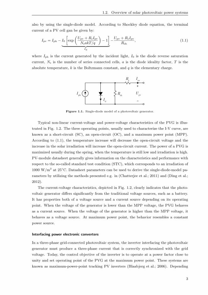
static electrical terminal characteristics of a PV cell can be represented by a single-diode model
depicted in Fig. 1.1. A current source Iph describes the current generated by the incident
light and a non-ideal diode represents the p-n junction inside the cell. Resistive losses Rs and
Rsh are included in the model to take into account the different terminal ohmic losses. Since
the PV module or array is a combination of series and/or parallel-connected single PV cells,
their current-voltage characteristics in uniform environmental conditions can be represented
2
1.2. Overview of solar photovoltaic power systems
also by using the single-diode model. According to Shockley diode equation, the terminal
current of a PV cell gan be given by:
Ipv = Iph − I0
[
exp
(Upv +RsIpvNsakT/q
)
− 1
]
︸ ︷︷ ︸Id
−Upv +RsIpv
Rsh, (1.1)
where Iph is the current generated by the incident light, I0 is the diode reverse saturation
current, Ns is the number of series connected cells, a is the diode ideality factor, T is the
absolute temperature, k is the Boltzmann constant, and q is the elementary charge.
phI
pvI
pvU
sR
shR
dI
Figure 1.1. Single-diode model of a photovoltaic generator.
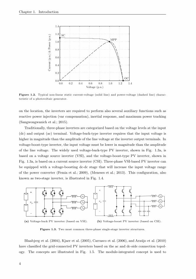
Typical non-linear current-voltage and power-voltage characteristics of the PVG is illus-
trated in Fig. 1.2. The three operating points, usually used to characterize the I-V curve, are
known as a short-circuit (SC), an open-circuit (OC), and a maximum power point (MPP).
According to (1.1), the temperature increase will decrease the open-circuit voltage and the
increase in the solar irradiation will increase the open-circuit current. The power of a PVG is
maximized usually during the spring, when the temperature is still low and irradiation is high.
PV-module datasheet generally gives information on the characteristics and performance with
respect to the so-called standard test condition (STC), which corresponds to an irradiation of
1000 W/m2 at 25C. Datasheet parameters can be used to derive the single-diode-model pa-
rameters by utilizing the methods presented e.g. in (Chatterjee et al.; 2011) and (Ding et al.;
2012).
The current-voltage characteristics, depicted in Fig. 1.2, clearly indicates that the photo-
voltaic generator differs significantly from the traditional voltage sources, such as a battery.
It has properties both of a voltage source and a current source depending on its operating
point. When the voltage of the generator is lower than the MPP voltage, the PVG behaves
as a current source. When the voltage of the generator is higher than the MPP voltage, it
behaves as a voltage source. At maximum power point, the behavior resembles a constant
power source.
Interfacing power electronic converters
In a three-phase grid-connected photovoltaic system, the inverter interfacing the photovoltaic
generator must produce a three-phase current that is correctly synchronized with the grid
voltage. Today, the control objective of the inverter is to operate at a power factor close to
unity and set operating point of the PVG at the maximum power point. These systems are
known as maximum-power-point tracking PV inverters (Blaabjerg et al.; 2006). Depending
3
Chapter 1. Introduction
0.0 0.2 0.4 0.6 0.8 1.0 1.2 1.40.0
0.2
0.4
0.6
0.8
1.0
1.2
1.4
Curr
ent
(p.u
.) &
Pow
er (
p.u
.)
Voltage (p.u.)
OC
SC
MPP
Figure 1.2. Typical non-linear static current-voltage (solid line) and power-voltage (dashed line) charac-
teristic of a photovoltaic generator.
on the location, the inverters are required to perform also several auxiliary functions such as
reactive power injection (var compensation), inertial response, and maximum power tracking
(Sangwongwanich et al.; 2015).
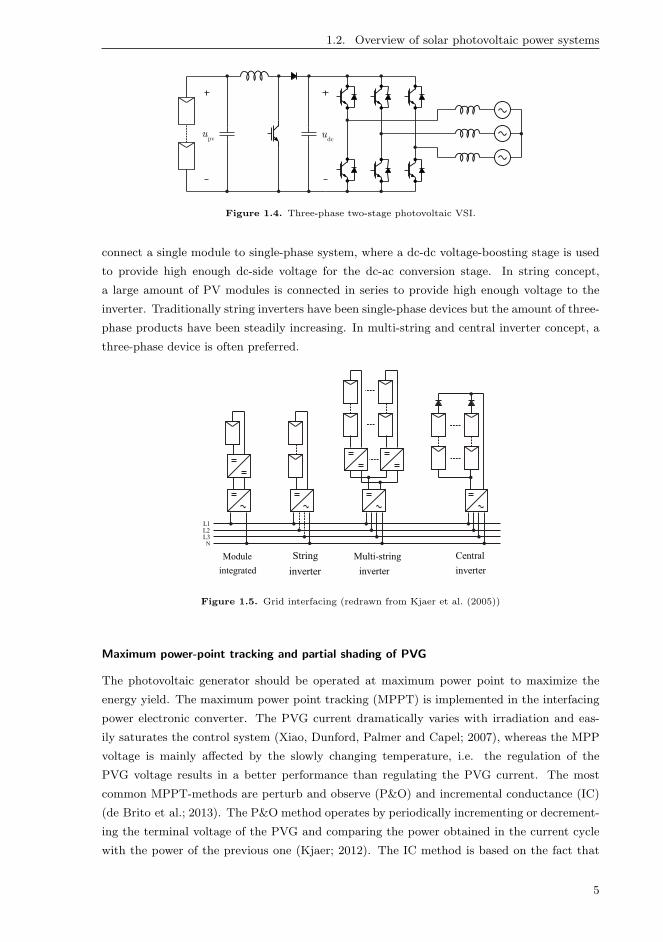
Traditionally, three-phase inverters are categorized based on the voltage levels at the input
(dc) and output (ac) terminal. Voltage-buck-type inverter requires that the input voltage is
higher in magnitude than the amplitude of the line voltage at the inverter output terminals. In
voltage-boost-type inverter, the input voltage must be lower in magnitude than the amplitude
of the line voltage. The widely used voltage-buck-type PV inverter, shown in Fig. 1.3a, is
based on a voltage source inverter (VSI), and the voltage-boost-type PV inverter, shown in
Fig. 1.3a, is based on a current source inverter (CSI). Three-phase VSI-based PV inverter can
be equipped with a voltage-boosting dc-dc stage that will increase the input voltage range
of the power converter (Femia et al.; 2009), (Meneses et al.; 2013). This configuration, also
known as two-stage inverter, is illustrated in Fig. 1.4.
pvu
(a) Voltage-buck PV inverter (based on VSI).
pvu
(b) Voltage-boost PV inverter (based on CSI).
Figure 1.3. Two most common three-phase single-stage inverter structures.
Blaabjerg et al. (2004), Kjaer et al. (2005), Carrasco et al. (2006), and Araujo et al. (2010)
have classified the grid-connected PV inverters based on the ac and dc-side connection topol-
ogy. The concepts are illustrated in Fig. 1.5. The module-integrated concept is used to
4
1.2. Overview of solar photovoltaic power systems
pvu
dcu
Figure 1.4. Three-phase two-stage photovoltaic VSI.
connect a single module to single-phase system, where a dc-dc voltage-boosting stage is used
to provide high enough dc-side voltage for the dc-ac conversion stage. In string concept,
a large amount of PV modules is connected in series to provide high enough voltage to the
inverter. Traditionally string inverters have been single-phase devices but the amount of three-
phase products have been steadily increasing. In multi-string and central inverter concept, a
three-phase device is often preferred.
L1L2L3
N
Module
integrated
String
inverter
Multi-string
inverter
Central
inverter
Figure 1.5. Grid interfacing (redrawn from Kjaer et al. (2005))
Maximum power-point tracking and partial shading of PVG
The photovoltaic generator should be operated at maximum power point to maximize the
energy yield. The maximum power point tracking (MPPT) is implemented in the interfacing
power electronic converter. The PVG current dramatically varies with irradiation and eas-
ily saturates the control system (Xiao, Dunford, Palmer and Capel; 2007), whereas the MPP
voltage is mainly affected by the slowly changing temperature, i.e. the regulation of the
PVG voltage results in a better performance than regulating the PVG current. The most
common MPPT-methods are perturb and observe (P&O) and incremental conductance (IC)
(de Brito et al.; 2013). The P&O method operates by periodically incrementing or decrement-
ing the terminal voltage of the PVG and comparing the power obtained in the current cycle
with the power of the previous one (Kjaer; 2012). The IC method is based on the fact that
5
Chapter 1. Introduction
the slope of the current-voltage curve, i.e. the dynamic resistance, corresponds to the static
resistance of the PVG at the maximum power point (Kjaer; 2012).
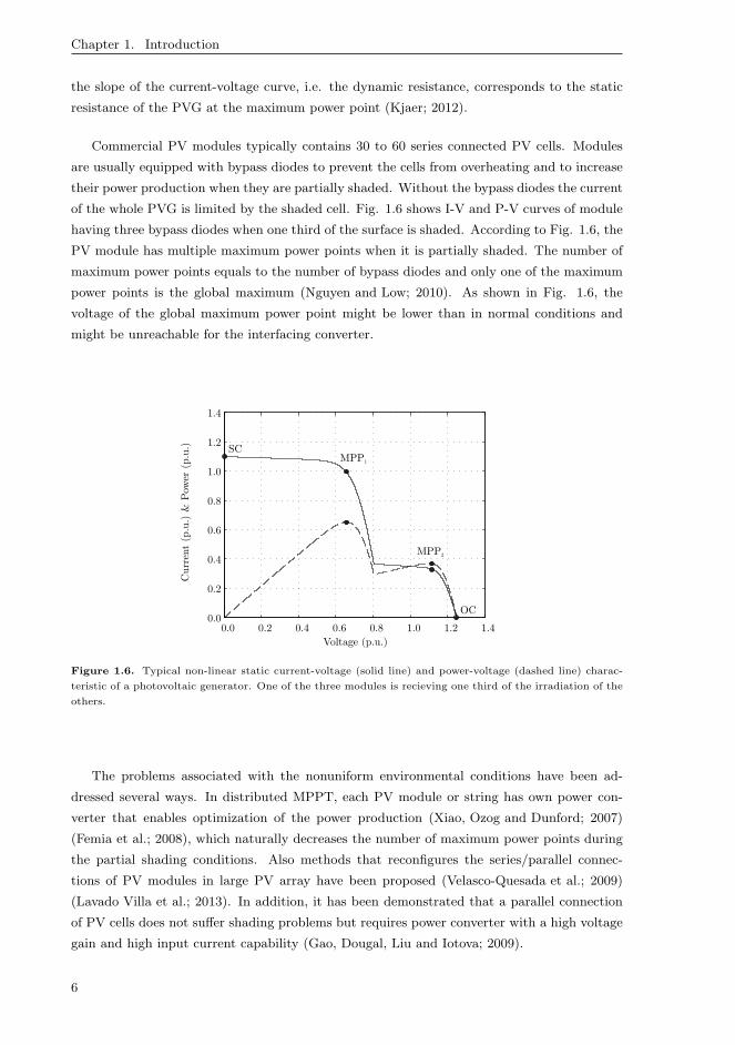
Commercial PV modules typically contains 30 to 60 series connected PV cells. Modules
are usually equipped with bypass diodes to prevent the cells from overheating and to increase
their power production when they are partially shaded. Without the bypass diodes the current
of the whole PVG is limited by the shaded cell. Fig. 1.6 shows I-V and P-V curves of module
having three bypass diodes when one third of the surface is shaded. According to Fig. 1.6, the
PV module has multiple maximum power points when it is partially shaded. The number of
maximum power points equals to the number of bypass diodes and only one of the maximum
power points is the global maximum (Nguyen and Low; 2010). As shown in Fig. 1.6, the
voltage of the global maximum power point might be lower than in normal conditions and
might be unreachable for the interfacing converter.
0.0 0.2 0.4 0.6 0.8 1.0 1.2 1.40.0
0.2
0.4
0.6
0.8
1.0
1.2
1.4
Curr
ent
(p.u
.) &
Pow
er (
p.u
.)
Voltage (p.u.)
MPP1
MPP2
OC
SC
Figure 1.6. Typical non-linear static current-voltage (solid line) and power-voltage (dashed line) charac-
teristic of a photovoltaic generator. One of the three modules is recieving one third of the irradiation of the
others.
The problems associated with the nonuniform environmental conditions have been ad-
dressed several ways. In distributed MPPT, each PV module or string has own power con-
verter that enables optimization of the power production (Xiao, Ozog and Dunford; 2007)
(Femia et al.; 2008), which naturally decreases the number of maximum power points during
the partial shading conditions. Also methods that reconfigures the series/parallel connec-
tions of PV modules in large PV array have been proposed (Velasco-Quesada et al.; 2009)
(Lavado Villa et al.; 2013). In addition, it has been demonstrated that a parallel connection
of PV cells does not suffer shading problems but requires power converter with a high voltage
gain and high input current capability (Gao, Dougal, Liu and Iotova; 2009).
6
1.3. Z-source inverter (ZSI)
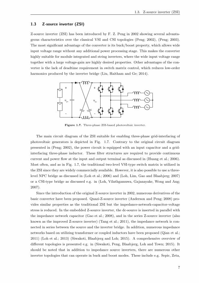
1.3 Z-source inverter (ZSI)
Z-source inverter (ZSI) has been introduced by F. Z. Peng in 2002 showing several advanta-
geous characteristics over the classical VSI and CSI topologies (Peng; 2002), (Peng; 2003).
The most significant advantage of the converter is its buck/boost property, which allows wide
input voltage range without any additional power processing stage. This makes the converter
highly suitable for module integrated and string inverters, where the wide input voltage range
together with a large voltage-gain are highly desired properties. Other advantages of the con-
verter is the lack of deadtime requirement in switch matrix control, which reduces low-order
harmonics produced by the inverter bridge (Liu, Haitham and Ge; 2014).
pvu
dcu
Figure 1.7. Three-phase ZSI-based photovoltaic inverter.
The main circuit diagram of the ZSI suitable for enabling three-phase grid-interfacing of
photovoltaic generators is depicted in Fig. 1.7. Contrary to the original circuit diagram
presented in (Peng; 2002), the power circuit is equipped with an input capacitor and a grid-
interfacing three-phase inductor. These filter structures are required to provide continuous
current and power flow at the input and output terminal as discussed in (Huang et al.; 2006).
Most often, and as in Fig. 1.7, the traditional two-level VSI-type switch matrix is utilized in
the ZSI since they are widely commercially available. However, it is also possible to use a three-
level NPC bridge as discussed in (Loh et al.; 2006) and (Loh, Lim, Gao and Blaabjerg; 2007)
or a CSI-type bridge as discussed e.g. in (Loh, Vilathgamuwa, Gajanayake, Wong and Ang;
2007).
Since the introduction of the original Z-source inverter in 2002, numerous derivatives of the
basic converter have been proposed. Quazi-Z-source inverter (Anderson and Peng; 2008) pro-
vides similar properties as the traditional ZSI but the impedance-network-capacitor-voltage
stress is reduced. In the embedded Z-source inverter, the dc-source is inserted in parallel with
the impedance network capacitor (Gao et al.; 2008), and in the series Z-source inverter (also
known as the improved Z-source inverter) (Tang et al.; 2011), the impedance network is con-
nected in series between the source and the inverter bridge. In addition, numerous impedance
networks based on utilizing transformer or coupled inductors have been proposed (Qian et al.;
2011) (Loh et al.; 2013) (Siwakoti, Blaabjerg and Loh; 2015). A comprehensive overview of
different topologies is presented e.g. in (Siwakoti, Peng, Blaabjerg, Loh and Town; 2015). It
should be noted that in addition to impedance source inverters, there are numerous other
inverter topologies that can operate in buck and boost modes. These include e.g. Sepic, Zeta,
7
Chapter 1. Introduction
and Cuk-converter-based inverters (Kikuchi and Lipo; 2002), switched boost (Upadhyay et al.;
2011), and diode assisted voltage-source inverter (Gao, Loh, Teodorescu and Blaabjerg; 2009).
Fundamentally, the ZSI operates as two-stage VSI, where the dc-link and the PVG voltage
can be controlled independently. The voltage-boosting property of the ZSI is achieved by in-
verter bridge shoot-through state that will alter the impedance network capacitor charge and
inductor flux-linkage balances. To include the required shoot-through state inside the mod-
ulation period of the inverter bridge, numerous different conventional (Loh et al.; 2005) and
space-vector-based (Liu, Ge, Abu-Rub and Peng; 2014) pulse-width modulation schemes have
been developed for the ZSI. The modulation method affects the ripple in the impedance net-
work inductor current (Shen et al.; 2006), the ripple in the capacitor voltage (Hanif et al.;
2011), the voltage stress of the components (Peng et al.; 2005), and the leakage current
(Bradaschia et al.; 2011). When the ZSI operates in voltage-buck mode, the impedance net-
work operates as an additional input filter and the same modulation methods as in VSI-type
inverter can be directly utilized.
As in the two stage inverter, the steady state value of the equivalent dc-link voltage can
be chosen arbitrary as long as it is higher than the amplitude of the grid line voltage and the
required shoot-through states can be inserted inside the modulation period. To minimize the
losses, the voltage should be as low as possible. However, due to the insertion of the shoot-
through states, the equivalent dc-link voltage (i.e. input voltage of the switching bridge) must
be increased when the ZSI operates in voltage-boosting mode. As a result, the ZSI efficiency
drops significantly when low input voltage is used (Wei et al.; 2011). The use of three-level
bridge can significantly reduce the losses compared to the two level bridge as discussed in
(Tenner and Hofmann; 2010).
Modeling and control of ZSI
One of the first dynamic model developed for the ZSI impedance-network-capacitor-voltage
control has been proposed in (Gajanayake et al.; 2005). Model was derived by using the con-
ventional state-space averaging technique. The authors observed that when the ZSI is supplied
from a voltage source, the transfer functions from the shoot-through duty cycle to the capacitor
voltage and equivalent dc-link voltage contains a right-half plane (RHP) zero. Later, the same
authors (Gajanayake et al.; 2007) showed that the effect of the RHP zero will propagate to the
control of the ac-side voltage of the converter and proposed a method to improve the transient
response. Similar results are provided in (Loh, Vilathgamuwa, Gajanayake, Lim and Teo;
2007). The authors in (Liu et al.; 2007) also observed an RHP zero and studied the location
of the system poles and zeros when parameters of the impedance network are altered. Later, an
average model based on circuit averaging technique is presented in (Galigekere and Kazimierczuk;
2013), which verified the results obtained by using the state-space models. The presence of
RHP zeros tends to destabilize the wide-bandwidth feedback loops, implying high-gain in-
stability and imposing control limitations. In addition, Upadhyay et al. (2011) have demon-
strated that the mismatch in the impedance network parameters may compromise the stability
of the capacitor voltage control due to the additional resonances and their effect on the phase
8
1.4. Motivation of the thesis
behavior of the control-to-capacitor voltage transfer function.
The use of Z-source inverter in PV applications was demonstrated in (Huang et al.; 2006)
and the control design in grid-connected applications is discussed e.g. in (Liu et al.; 2013),
(Gajanayake et al.; 2009), and Li et al. (2010). In grid-connected applications, the capacitor
voltage control is the recommended control scheme of the inverter instead of the equivalent
dc-link voltage control. The drawbacks of a equivalent dc-link voltage control have been
discussed in (Tang et al.; 2010) and Li et al. (2010). The equivalent dc-link waveform is
a pulsed waveform due to shoot-through states and the equivalent dc-link voltage reference
should be modified according to the shoot-through duty cycle, whereas the impedance network
capacitor voltage reference can be kept constant. Moreover, in the capacitor voltage control,
the equivalent dc-link voltage is automatically as low as possible and the inverter bridge
switching losses are minimized.
1.4 Motivation of the thesis
Small-signal modeling of switched-mode power converters has been widely studied topic since
1980s Middlebrook and Cuk (1977) since it provides deterministic methods to evaluate the
performance of the converter under different control modes (Middlebrook; 1988). In addi-
tion, by using the small-signal model the impedance characteristics of the converter can be
derived, which provides a simple tool to analyze the operation of the converter as a part of
an interconnected system. Small-signal based modeling also enables taking into account the
dual nature (highly non-linear current-voltage characteristics) of the PVG in control design
of the interfacing power electronic converters, which will improve the control system quality
as discussed in (Suntio et al.; 2009) (Suntio et al.; 2010). It is claimed that the small-signal
methods have increased the product quality of a dc-dc converters significantly. Thus it is quite
natural that an increased interest towards the small-signal methods for ac-systems have been
observed as the number of electric systems with power-converter-based sources and loads is
constantly increasing.
Grid-connected inverters have been shown to increase the harmonic distortion in the grid
(Enslin and Heskes; 2004) and may even compromise the system stability (Wan et al.; 2013).
To analyze these interactions, an impedance-based stability-criteria have been proposed (Sun;
2011). The measured impedance provides tools to analyze the interactions, although the
measurements may be difficult to be implement in practice. Thus the models that can predict
the impedance characteristics are highly desirable. In this thesis, a model to predict the
output impedance of a ZSI is also proposed.
The single and two-stage VSI-based photovoltaic inverter have been demonstrated to con-
tain a RHP-zero in the output current control when the converter is fed from a source having
characteristics of a current-source. The presence of the RHP-zero will destabilize the con-
trol system of the inverter when wide bandwidth current control is utilized. Fortunately
a dc-link voltage control with a sufficient bandwidth depending on the size of the dc-link
capacitor can stabilize the inverter control system (Messo et al.; 2014). Due to the simi-
larities in the converter topologies, a same tradeoff will be present also in ZSI. Component
9
Chapter 1. Introduction
selection of the Z-source inverter impedance network have been discussed e.g. in (Liu et al.;
2007), (Rajakaruna and Jayawickrama; 2010), and (Liu, Ge, Abu-Rub and Peng; 2014). In
this thesis, a requirement for the impedance network capacitor is discussed to guarantee the
small-signal stability.
1.5 Scientific contribution
The scientific contribution of the thesis can be summarized as:
• It was shown that the voltage-fed small-signal model fails to predict the small-signal
characteristics of a grid-connected Z-source inverter when it is supplied from a source
having high impedance (e.g. photovoltaic generator operating at current region). A
small-signal model that takes into account the effect of the non-ideal source was derived.
• Based on the derived small-signal model, a design rule for the minimum value of the
impedance network capacitor to guarantee the stable operation of ZSI was formulated.
This limitation is removed if a feedback control system regulating the input voltage of
the ZSI is utilized.
• A model to evaluate the effect of the asymmetric impedance network to the behavior of
the inverter is derived. The mismatch in the impedance network components will cause
additional resonances in the impedance network and result undesired oscillations during
the disturbances. However, these oscillations are negligible and not visible at the input
and output terminals of the converter.
• Differences between the dynamic properties of ZSI and VSI (single and two-stage) are
presented. It is concluded that the dynamic properties of photovoltaic ZSI is comparable
to VSI-based two-stage PV inverter.
Related papers
The ideas presented in this thesis are partly presented in the following publications:
[P1] Jokipii, J. and Suntio, T. ’Input voltage control of a three-phase Z-source inverter in
photovoltaic applications’, in IEEE PEDG 2013, Rogers, AR, USA. pp 1-8.
[P2] Jokipii, J., Messo, T and Suntio, T. ’Simple method for measuring output impedance
of a three-phase inverter in dq-domain’, in IEEE IPEC 2014, Hirosima, Japan, pp.
1466–1470.
[P3] Jokipii, J. and Suntio, T. ’Dynamic characteristics of three-phase Z-source-based pho-
tovoltaic inverter with asymmetric impedance network’, in IEEE ICPE 2015, Seoul,
South-Korea, pp. 1976–1983.
[P4] Messo, T., Jokipii, J., Puukko, J. and Suntio, T. ’Determining the value of DC-link
capacitance to ensure stable operation of a three-phase photovoltaic inverter’, in IEEE
Trans. Power Electron., vol. 29, no. 2, pp. 665-673, 2014.
10
1.6. Structure of the thesis
[P5] Messo, T., Jokipii, J., Makinen, A., and Suntio, T. ’Modeling the grid synchronization
induced negative-resistor-like behavior in the output impedance of a three-phase photo-
voltaic inverter’, in IEEE PEDG 2013, Rogers, AR, USA, pp. 1-7.
In [P1], [P2], and [P3] author carried out the presented analysis, designed and built the
prototype converter, and conducted the laboratory measurements. Dr. Tech. Messo helped
with the proofreading, implementing the required laboratory setup, and the actual laboratory
measurements. Prof. Suntio as a supervisor of the conducted research provided valuable
ideas and comments regarding the analysis and terminology related to small-signal modeling
of power converters and writing publications. In [P4] and [P5], where the main author was
Dr. Tech. Messo, the author designed and built part of the required laboratory setup and
helped with proofreading the papers. The author also contributed to the analysis carried out
in [P4] and [P5].
1.6 Structure of the thesis
Chapter 2 presents the background of the thesis by introducing a method to derive small-
signal model for single and two-stage VSI-based PV inverter by combining model of a voltage-
fed VSI and the source subsystems. In Chapter 3, the same voltage-fed VSI model is used
to develop the model of a voltage-fed and current-fed ZSI. Chapter 4 presents model for
a photovoltaic ZSI and discusses the control design issues related to the inverter. Chapter
5 provides comparison between the dynamic properties of the ZSI and the VSI-based PV
inverters. Finally conclusions and recommended future topics are presented in Chapter 6.
11

12
2 DYNAMIC CHARACTERIZATION OF VOLTAGE-SOURCE
INVERTERS
This chapter introduces the small-signal modeling method used in this thesis by presenting
a model for a grid-connected three-phase voltage-source inverter (VSI), which will be further
developed to represent the small-signal characteristics of a single and a two-stage VSI-based
photovoltaic inverter and Z-source inverter (ZSI).
2.1 On small-signal modeling of interfacing power electronic converters
Interfacing power electronic converters transfer energy between two electrical system, the
source and load. Often, these interfacing converters are classified only based on the voltage
levels at the input and output terminals, phase number, or type of system (dc or ac) but the
fundamental nature of the source and load subsystem is usually neglected. Neglecting the
behavior of the source and load may be justified when the static steady-state operation of
the converter is analyzed, e.g. when studying efficiency or pulse-width modulation methods,
since they do not affect to the results. However, when the dynamic behavior of the converters
are analyzed, the type of load and source will affect the results and must be thus taken into
account. Each interfacing power converter inherits four conversion schemes that are dictated
by the type of source, load, and control-mode (Suntio et al.; 2009), (Suntio et al.; 2014). These
conversion schemes together with the corresponding two-port network models are introduced
in Fig. 2.1.
In the state-space-averaging and circuit-averaging techniques, the non-linear nature of a
switched-mode power converter is removed by linearizing the operation of the converter at a
steady-state operation point (Middlebrook; 1988), (Krein et al.; 1989). However, in the ac-
systems, the steady state is sinusoidal, which effectively prevents using these methods as such.
To overcome this limitation, several different methods to analyze the power converters in ac
systems have been proposed. These include harmonic linearization (Sun; 2009), dynamic pha-
sor theory (Mattavelli et al.; 1999), complex transfer functions (Gataric and Garrigan; 1999)
and (Harnefors; 2007), and synchronous-reference-frame-based modeling (Hiti and Boroyevich;
1996). In synchronous-reference-frame-based modeling (dq-domain modeling), the sinusoidal
quantities at the fundamental operating frequency are represented by constants, which allows
applying conventional state-space-averaging techniques. It is worth noting that a conventional
phasor theory including concept of symmetric components applies only to linear circuits oper-
ating at steady state. Nevertheless, it has been proven to be suitable for utility-power-system
13
Chapter 2. Dynamic characterization of voltage-source inverters
inu o
u
ini
oi
G
(a) Voltage-to-voltage (G-parameter model).
inu o
u
ini
oi
Y
(b) Voltage-to-current (Y-parameter model).
inu o
u
ini
oi
H
(c) Current-to-current (H-parameter model).
inu o
u
ini
oi
Z
(d) Current-to-voltage (Z-parameter model).
Figure 2.1. Four conversion schemes suitable for analyzing dynamic characteristics of interfacing power
converters.
analysis for e.g. stability analysis of transmission lines and loads under the assumption that
the amplitudes of voltages and currents change slowly with time such that their time deriva-
tives can be assumed zero. The power converters, on the other hand, have high-bandwidth
control loops and thus the conventional phasor theory is suitable only for steady-state analysis
(Sun; 2009).
In grid-connected applications, the load of the power converter is the utility grid, which in
an ideal case has a zero line impedance. In addition, in order to obtain high-quality currents,
the power converters must be equipped with a high-bandwidth current control, hence the
recommended conversion schemes to analyze dynamic behavior of a grid-connected power
converter are the Y and H-parameter models (i.e. the voltage-to-current and current-to-
current conversion schemes). Moreover, if the power converter is equipped with an input
side voltage feedback control, as a photovoltaic inverter, it should be analyzed using the
current-to-current conversion scheme (H-parameter model). Hence, the inverter interfacing
the photovoltaic generators should be analyzed as a current-fed system. Unfortunately, this
may cause misunderstanding as the inverters have been earlier classified as voltage-source
and current-source inverter, based on the inverter power-stage-circuit structure instead of
the type of the electrical energy source. The term voltage-source inverter (VSI) refers to
the inverter bridge (switch matrix) topology, which requires that the dc-side voltage across
the switch matrix retains its polarity and stays nearly constant during one switching period.
Correspondingly, the current-source inverter (CSI) refers to the bridge, where the switch
matrix dc-side current retains its polarity. To avoid misinterpretation, in this thesis, the term
VSI is used to refer to the bridge topology, whereas term VSI-based inverter refers to a power
converter, which contains the VSI-type inverter bridge and filter structures to comply with
the requirements of the source and load.
14
2.1. On small-signal modeling of interfacing power electronic converters
Photovoltaic generator as an input source
As discussed in Chapter 1, the photovoltaic generator (PVG) is a highly non-linear source
having properties of a current source and a voltage source. Its small-signal behavior have
been demonstrated to behave as a simple RLC-circuit, whose parameters vary depending
on the operation point. However, the impedance of the reactive components are relatively
small compared to the impedance of the input capacitors typically used in power converters
(Nousiainen et al.; 2013). Thus when the interconnected system of a photovoltaic generator
and interfacing power converter is analyzed, the output impedance of the PVG can be ap-
proximated using its low-frequency value, i.e. the dynamic resistance (rpv = upv/ipv). The
value of dynamic resistance varies from several ohms to several hundreds of ohms depending
on the shape of the current-voltage curve and equals the static resistance (Rpv = Upv/Ipv) at
the maximum power point as illustrated in Fig. 2.2.
0.0 0.2 0.4 0.6 0.8 1.0 1.2 1.4 0.0
0.2
0.4
0.6
0.8
1.0
1.2
1.4
MPP
Curr
ent
(p.u
.) &
Pow
er (
p.u
.)
Voltage (p.u.)
(a) Current-voltage (solid line) and power-voltage
(dashed line) characteristics.
0.0 0.2 0.4 0.6 0.8 1.0 1.2 1.4 0.0
5.0
10.0
15.0
20.0
25.0
30.0
35.0
40.0
MPP
Res
ista
nce
(p.u
.)
Voltage (p.u.)
(b) Static (solid line) and dynamic (dashed line)
resistance.
Figure 2.2. Electrical characteristics of a photovoltaic generator (PVG).
Three-phase VSI-based photovoltaic inverter
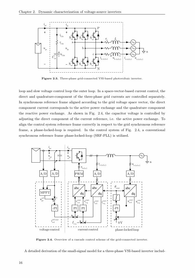
The power stage of a widely used three-phase inverter structure, a VSI-based inverter, is
illustrated in Fig. 2.3 inside a dashed line. The inverter consists of an input capacitor (also
known as the dc-link capacitor), VSI-type inverter bridge, and the grid-interfacing filter. In
pulse-width-modulated power converter, the state of inverter bridge transistor is controlled
by a pulse-width modulation & gate drive circuit, and operated by the control system of
the inverter. The internal structure of the control system varies depending on the application
(Blaabjerg et al.; 2006), however, it usually includes at least a high-bandwidth current control
and grid synchronization.
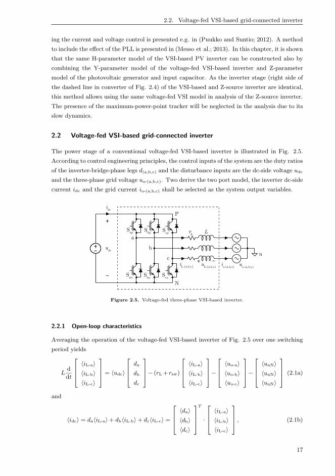
In this thesis, the control scheme, which is illustrated in Fig. 2.4, is analyzed, in which the
control objective is to set the operating point of the photovoltaic generator to its maximum
power point. This is achieved by controlling the inverter dc-side capacitor voltage through a
cascade connected feedback loops, where the fast current control forms the innermost control
15
Chapter 2. Dynamic characterization of voltage-source inverters
Lr L
o-(a,b,c)i
o-(a,b,c)u
L-(a,b,c)u
dcu
a
b
cn
L-(a,b,c)i
N
Pdci
cpS
bpS
apS
cnS
bnS
anS
pvi
dcC
Cdcu
pvu
Cdcr
Cdci
Figure 2.3. Three-phase grid-connected VSI-based photovoltaic inverter.
loop and slow voltage control loop the outer loop. In a space-vector-based current control, the
direct and quadrature-component of the three-phase grid currents are controlled separately.
In synchronous reference frame aligned according to the grid voltage space vector, the direct
component current corresponds to the active power exchange and the quadrature component
the reactive power exchange. As shown in Fig. 2.4, the capacitor voltage is controlled by
adjusting the direct component of the current reference, i.e. the active power exchange. To
align the control system reference frame correctly in respect to the grid synchronous reference
frame, a phase-locked-loop is required. In the control system of Fig. 2.4, a conventional
synchronous reference frame phase-locked-loop (SRF-PLL) is utilized.
-PI
0V
ò
convq
conv
o-du conv
o-qu
dq
abc
conv
o-di
conv
o-qi
conv
c-dv
conv
c-qv
PI PI
ref-conv
o-di
o-qI
(a,b,c)s
///
o-(a,b,c)i
///
A/D
///
/// o-(a,b,c)
u
///
A/D
/// n
dq
abc
dq
abc
///
phase-locked loopcurrentcontrol
A/D
-PI
ref
pvu
voltage control
pvu
pvi
dci
dcu
A/D
MPPT
PWM
Figure 2.4. Overview of a cascade control scheme of the grid-connected inverter.
A detailed derivation of the small-signal model for a three-phase VSI-based inverter includ-
16
2.2. Voltage-fed VSI-based grid-connected inverter
ing the current and voltage control is presented e.g. in (Puukko and Suntio; 2012). A method
to include the effect of the PLL is presented in (Messo et al.; 2013). In this chapter, it is shown
that the same H-parameter model of the VSI-based PV inverter can be constructed also by
combining the Y-parameter model of the voltage-fed VSI-based inverter and Z-parameter
model of the photovoltaic generator and input capacitor. As the inverter stage (right side of
the dashed line in converter of Fig. 2.4) of the VSI-based and Z-source inverter are identical,
this method allows using the same voltage-fed VSI model in analysis of the Z-source inverter.
The presence of the maximum-power-point tracker will be neglected in the analysis due to its
slow dynamics.
2.2 Voltage-fed VSI-based grid-connected inverter
The power stage of a conventional voltage-fed VSI-based inverter is illustrated in Fig. 2.5.
According to control engineering principles, the control inputs of the system are the duty ratios
of the inverter-bridge-phase legs d(a,b,c) and the disturbance inputs are the dc-side voltage udc
and the three-phase grid voltage uo-(a,b,c). Two derive the two port model, the inverter dc-side
current idc and the grid current io-(a,b,c) shall be selected as the system output variables.
Lr L
o-(a,b,c)i
o-(a,b,c)u
L-(a,b,c)u
dcu
a
b
cn
L-(a,b,c)i
N
Pdci
cpS
bpS
apS
cnS
bnS
anS
Figure 2.5. Voltage-fed three-phase VSI-based inverter.
2.2.1 Open-loop characteristics
Averaging the operation of the voltage-fed VSI-based inverter of Fig. 2.5 over one switching
period yields
Ld
dt
〈iL-a〉
〈iL-b〉
〈iL-c〉
= 〈udc〉
da
db
dc
− (rL+ rsw)
〈iL-a〉
〈iL-b〉
〈iL-c〉
−
〈uo-a〉
〈uo-b〉
〈uo-c〉
−
〈unN〉
〈unN〉
〈unN〉
(2.1a)
and
〈idc〉 = da〈iL-a〉+ db〈iL-b〉+ dc〈iL-c〉 =
〈da〉
〈db〉
〈dc〉
T
·
〈iL-a〉
〈iL-b〉
〈iL-c〉
, (2.1b)
17

Chapter 2. Dynamic characterization of voltage-source inverters
where d(a,b,c) are the duty ratios of each phase leg, rsw is the on-state resistance of the
transistor and its anti-parallel diode (assumed to be equal), and unN is the zero-sequence
voltage produced by the inverter bridge. In (2.1), the angle brackets are used to represent the
moving average of the corresponding quantity (averaged over one switching cycle).
The average model of the inverter, given in (2.1), may be written as an equivalent two-phase
system in synchronous reference frame by applying the transformations presented explicitly in
Appendix A. Zero sequence is neglected, since due to three-wire connection the zero sequence
current cannot flow. The model in the synchronous reference frame can be given by
Ld
dt
[
〈iL-d〉
〈iL-q〉
]
=
[
−(rL + rsw) ωsL
−ωsL −(rL + rsw)
][
〈iL-d〉
〈iL-q〉
]
+ 〈udc〉
[
dd
dq
]
−
[
〈uo-d〉
〈uo-q〉
]
(2.2a)
and
〈idc〉 =3
2
[
dd
dq
]T
·
[
〈iL-d〉
〈iL-q〉
]
. (2.2b)
In synchronous reference frame, the steady-state operating point is represented by constant
quantities enabling the use of conventional linearization methods. In grid-connected inverter,
the steady-state values of the dc-side voltage, dc-side current, and grid voltage are usually
known, which can be used to obtain the linearization point (steady state) values of the duty
cycles and output current by setting the time-derivatives in (2.2) to zero. The steady state
operating point can be solved by using the equations
D2d +
2ωsLIo-q − Uo-d
UdcDd +
(ω2sL
2 +R2dc)I
2o-q − ωsLUo-dIo-q
U2dc
−2IinReq
3Udc= 0 V (2.3a)
Io-d =DdUdc + ωsLIo-q − Uo-d
Req(2.3b)
Dq =ωsLIo-d +ReqIo-q
Udc(2.3c)
Req = rL + rsw, Uo-q = 0 V, IL-d = Io-d, IL-q = Io-q =3
2Uo-dQ, (2.3d)
where Q is the steady-state value of the reactive power drawn by the inverter (usually set to
zero). In synchronous reference frame aligned to grid-voltage space vector, the steady-state
value of the grid-voltage q-component is zero.
The average model of (2.2) can be linearized at the steady-state operating point given by
(2.3) resulting a linearized state-space model of the inverter. The linearized model in Laplace
18
2.2. Voltage-fed VSI-based grid-connected inverter
domain using conventional state-space representation can be given by
s
[
iL-d
iL-q
]
︸ ︷︷ ︸x
=
[
− rL+rsw
Lωs
−ωs − rL+rsw
L
]
︸ ︷︷ ︸A
[
iL-d
iL-q
]
︸ ︷︷ ︸x
+
[Dd
L− 1
L0 Udc
L0
Dq
L0 − 1
L0 Udc
L
]
︸ ︷︷ ︸B
udc
uo-d
uo-q
dd
dq
︸ ︷︷ ︸u
(2.4a)
and
idc
io-d
io-q
︸ ︷︷ ︸y
=
3Dd
2
3Dq
2
1 0
0 1
︸ ︷︷ ︸C
[
iL-d
iL-q
]
︸ ︷︷ ︸x
+
0 0 0 3Io-d2
3Io-q2
0 0 0 0 0
0 0 0 0 0
︸ ︷︷ ︸D
udc
uo-d
uo-q
dd
dq
︸ ︷︷ ︸u
, (2.4b)
where x presents the state variables, u the input variables, and y the output variables. Thus
the inverter model can be formulated as
sx = Ax+Bu
y = Cx+Du.(2.5)
Transfer functions of the voltage-fed VSI-based inverter
The state space representation given in (2.5) provides a simple method to compute all the
transfer functions of the inverter. The system output as a function of the input variables can
be solved using (2.6). Due to the complexity of the system, matrix manipulation software
such as MATLAB is required to perform the computation.
y =[C (sI−A)−1 B+D
]u = Gu (2.6)
Since the system has five input variables and three output variables a total of fifteen trans-
fer functions is obtained as shown in (2.7). These transfer functions are presented explicitly
in Appendix B.
idc
io-d
io-q
︸ ︷︷ ︸y
=
Yin Toi-d Toi-q Gci-d Gci-q
Gio-d −Yo-d −Yo-qd Gco-d Gco-qd
Gio-q −Yo-dq −Yo-q Gco-dq Gco-q
︸ ︷︷ ︸G
udc
uo-d
uo-q
dd
dq
︸ ︷︷ ︸u
(2.7)
19
Chapter 2. Dynamic characterization of voltage-source inverters
Using the derived transfer functions, the input and the output dynamics of the converter
can be given by
idc = Yinudc + Toi-duo-d + Toi-quo-q +Gci-ddd +Gci-qdq (2.8)
and
io-d = Gio-dudc − Yo-duo-d − Yo-qduo-q +Gco-ddd +Gco-qddq
io-q = Gio-qudc − Yo-dquo-d − Yo-quo-q +Gco-dqdd +Gco-qdq, (2.9)
respectively. The output terminal of the model is divided into direct and quadrature compo-
nents, i.e. the model has three terminals. Fortunately, the complexity of the model can be
reduced by utilizing transfer matrices to represent the input and output dynamics
idc = Yinudc +[
Toi-d Toi-q
]
︸ ︷︷ ︸Toi
[
uo-d
uo-q
]
+[
Gci-d Gci-q
]
︸ ︷︷ ︸Gci
[
dd
dq
]
(2.10)
and
[
io-d
io-q
]
=
[
Gio-d
Gio-q
]
︸ ︷︷ ︸Gio
udc −
[
Yo-d Yo-qd
Yo-dq Yo-q
]
︸ ︷︷ ︸Yo
[
uo-d
uo-q
]
+
[
Gco-d Gco-qd
Gco-dq Gco-q
]
︸ ︷︷ ︸Gco
[
dd
dq
]
. (2.11)
Furthermore, the use of transfer matrices can be utilized to obtain a linear two-port model
(2.12), which can be visualized by an equivalent circuit shown in Fig. 2.6 or control-block
diagram shown in Fig 2.7. The notations are the same that has been successfully used to
analyze the dc-dc converters.
[
idc
io
]
=
[
Yin Toi Gci
Gio −Yo Gco
]
udc
uo
d
(2.12)
dci
dcu
inY ci-d
ˆG doi oˆT u
d
oi dcuG
coˆG d
oY
ou
oi
Figure 2.6. Linear two-port model of voltage-fed grid-connected inverter.
20
2.2. Voltage-fed VSI-based grid-connected inverter
inY
oiT
ioG
o-Y
coG
ciG
d
dci
oi
dcu
ou
Figure 2.7. Control-block diagram representing the open-loop dynamics of voltage-fed VSI-based inverter.
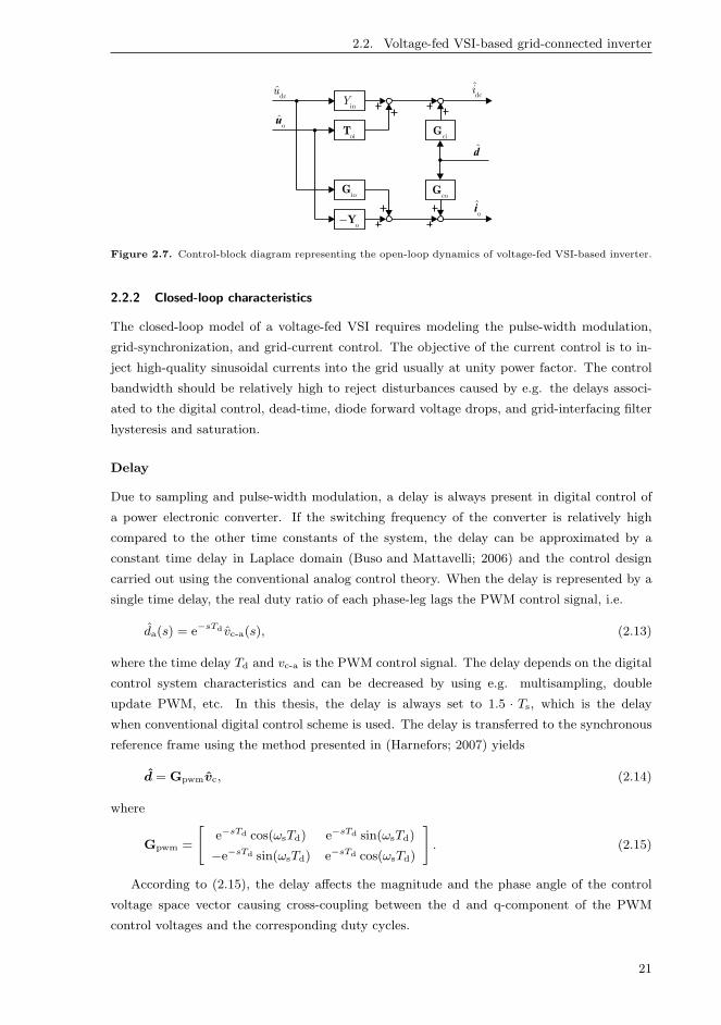
2.2.2 Closed-loop characteristics
The closed-loop model of a voltage-fed VSI requires modeling the pulse-width modulation,
grid-synchronization, and grid-current control. The objective of the current control is to in-
ject high-quality sinusoidal currents into the grid usually at unity power factor. The control
bandwidth should be relatively high to reject disturbances caused by e.g. the delays associ-
ated to the digital control, dead-time, diode forward voltage drops, and grid-interfacing filter
hysteresis and saturation.
Delay
Due to sampling and pulse-width modulation, a delay is always present in digital control of
a power electronic converter. If the switching frequency of the converter is relatively high
compared to the other time constants of the system, the delay can be approximated by a
constant time delay in Laplace domain (Buso and Mattavelli; 2006) and the control design
carried out using the conventional analog control theory. When the delay is represented by a
single time delay, the real duty ratio of each phase-leg lags the PWM control signal, i.e.
da(s) = e−sTd vc-a(s), (2.13)
where the time delay Td and vc-a is the PWM control signal. The delay depends on the digital
control system characteristics and can be decreased by using e.g. multisampling, double
update PWM, etc. In this thesis, the delay is always set to 1.5 · Ts, which is the delay
when conventional digital control scheme is used. The delay is transferred to the synchronous
reference frame using the method presented in (Harnefors; 2007) yields
d = Gpwmvc, (2.14)
where
Gpwm =
[
e−sTd cos(ωsTd) e−sTd sin(ωsTd)
−e−sTd sin(ωsTd) e−sTd cos(ωsTd)
]
. (2.15)
According to (2.15), the delay affects the magnitude and the phase angle of the control
voltage space vector causing cross-coupling between the d and q-component of the PWM
control voltages and the corresponding duty cycles.
21

Chapter 2. Dynamic characterization of voltage-source inverters
Phase-locked loop
The block-diagram of a conventional synchronous-reference-frame phase-locked loop (SRF-
PLL) was illustrated previously in Fig. 2.4. The inputs of the PLL are the measured phase
or line voltages and the output is the instantaneous electrical angle of the grid voltage space
vector. For determining the instantaneous angle of the grid-voltage space vector, it is assumed
that the quadrature component of the grid-voltage in SRF is zero.
Previously, the model of the inverter was derived in the synchronous-reference frame ro-
tating at a constant frequency. The block-diagram of the conventional phase-locked loop
represented in the same synchronous reference frame is shown in Fig. 2.8. At the steady
state, the angles of the synchronous reference frame (θgrid) and the control system reference
frame (θconv) are equal. However, if a perturbation is added to the quadrature component
of the grid voltage (e.g. due to unbalance or frequency deviation), the PLL will adjust the
control-system-reference-frame electrical angle accordingly.
convw
sdq
cdq 1/ s
conv
o-du
conv
o-qu
qD
o-du
o-qu
1/ ss
wconv
qgrid
q0V
pll
cG
Figure 2.8. Synchronous reference frame phase-locked loop. Inputs in synchronous reference frame.
As discussed in (Messo et al.; 2013), the PLL small-signal model shown in Fig. 2.9, which is
suitable for the control design of the PLL controller, can be obtained by linearizing the space-
vector transformation mapping the quantities between the synchronous reference frame and
control system reference frame. Transferring arbitrary quantity x(d,q) between the synchronous
reference frame and control system reference frame (denoted by superscript conv) is defined
as follows (see Appendix A):
xconvd = cos θ∆xd + sin θ∆xq (2.16a)
and
xconvq = − sin θ∆xd + cos θ∆xq, (2.16b)
where the angle difference between the synchronous reference frame and control system
reference frame is θ∆ = θconv − θgrid. Linearizing (2.16) yields
xconvd = xd + θ∆Xq (2.17a)
and
xconvq = xq − θ∆Xd. (2.17b)
22
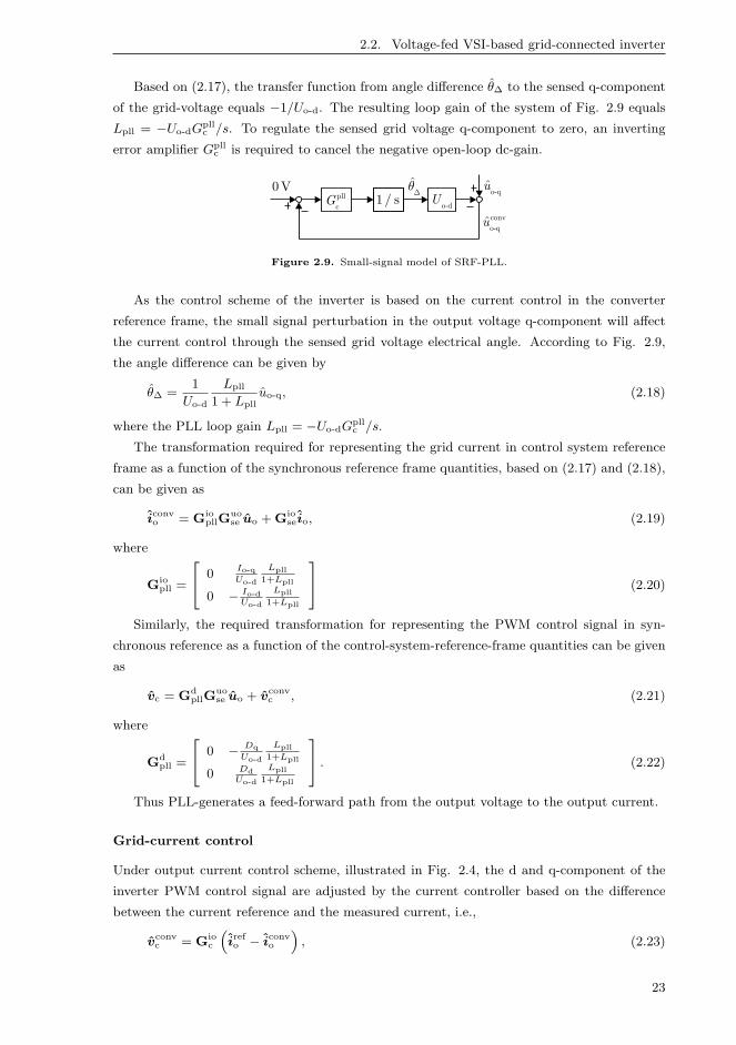
2.2. Voltage-fed VSI-based grid-connected inverter
Based on (2.17), the transfer function from angle difference θ∆ to the sensed q-component
of the grid-voltage equals −1/Uo-d. The resulting loop gain of the system of Fig. 2.9 equals
Lpll = −Uo-dGpllc /s. To regulate the sensed grid voltage q-component to zero, an inverting
error amplifier Gpllc is required to cancel the negative open-loop dc-gain.
o-dU
pll
cG 1/ s
conv
o-qu
qD0V o-q
u
Figure 2.9. Small-signal model of SRF-PLL.
As the control scheme of the inverter is based on the current control in the converter
reference frame, the small signal perturbation in the output voltage q-component will affect
the current control through the sensed grid voltage electrical angle. According to Fig. 2.9,
the angle difference can be given by
θ∆ =1
Uo-d
Lpll
1 + Lplluo-q, (2.18)
where the PLL loop gain Lpll = −Uo-dGpllc /s.
The transformation required for representing the grid current in control system reference
frame as a function of the synchronous reference frame quantities, based on (2.17) and (2.18),
can be given as
iconvo = Gio
pllGuose uo +Gio
seio, (2.19)
where
Giopll =
0
Io-q
Uo-d
Lpll
1+Lpll
0 − Io-d
Uo-d
Lpll
1+Lpll
(2.20)
Similarly, the required transformation for representing the PWM control signal in syn-
chronous reference as a function of the control-system-reference-frame quantities can be given
as
vc = GdpllG
uose uo + v
convc , (2.21)
where
Gdpll =
0 −
Dq
Uo-d
Lpll
1+Lpll
0 Dd
Uo-d
Lpll
1+Lpll
. (2.22)
Thus PLL-generates a feed-forward path from the output voltage to the output current.
Grid-current control
Under output current control scheme, illustrated in Fig. 2.4, the d and q-component of the
inverter PWM control signal are adjusted by the current controller based on the difference
between the current reference and the measured current, i.e.,
vconvc = Gio
c
(
irefo − i
convo
)
, (2.23)
23
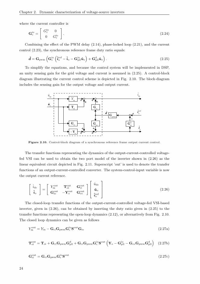
Chapter 2. Dynamic characterization of voltage-source inverters
where the current controller is
Gioc =
[
Gioc 0
0 Gioc
]
. (2.24)
Combining the effect of the PWM delay (2.14), phase-locked loop (2.21), and the current
control (2.23), the synchronous reference frame duty ratio equals:
d = Gpwm
(
Gioc
(
irefo − io −Gio
plluo
)
+Gdplluo
)
. (2.25)
To simplify the equations, and because the control system will be implemented in DSP,
an unity sensing gain for the grid voltage and current is assumed in (2.25). A control-block
diagram illustrating the current control scheme is depicted in Fig. 2.10. The block-diagram
includes the sensing gain for the output voltage and output current.
inY
oiT
ioG
o-Y
coG
ciG
d
dci
oi
dcu
ou
pwmG
io
seG
ref
oi
Figure 2.10. Control-block diagram of a synchronous reference frame output current control.
The transfer functions representing the dynamics of the output-current-controlled voltage-
fed VSI can be used to obtain the two port model of the inverter shown in (2.26) as the
linear equivalent circuit depicted in Fig. 2.11. Superscript ’out’ is used to denote the transfer
functions of an output-current-controlled converter. The system-control-input variable is now
the output current reference.
[
idc
io
]
=
[
Y outin Tout
oi Goutri
Goutio −Yout
o Goutro
]
udc
uo
irefo
(2.26)
The closed-loop transfer functions of the output-current-controlled voltage-fed VSI-based
inverter, given in (2.26), can be obtained by inserting the duty ratio given in (2.25) to the
transfer functions representing the open-loop dynamics (2.12), or alternatively from Fig. 2.10.
The closed loop dynamics can be given as follows
Y outin = Yin −GciGpwmGio
c SoutGio (2.27a)
Toutoi = Toi +GciGpwmGd
pll +GciGpwmGioc S
out(
Yo −Giopll −GcoGpwmGd
pll
)
(2.27b)
Goutri = GciGpwmGio
c Sout (2.27c)
24
2.2. Voltage-fed VSI-based grid-connected inverter
Goutio = SoutGio (2.27d)
Youto = SoutYo +ToutG
iopll − SoutGcoGpwmGd
pll (2.27e)
Goutro = Tout (2.27f)
where the sensitivity function can be given by
Sout = (I+GcoGpwmGioc )
−1 (2.28)
and the input-to-output transfer matrix by
Tout = GcoGpwmGioc (I+GcoGpwmGio
c )−1. (2.29)
dci
dcu
out
inY
out ref
ci oˆG i
out
oi oˆT u
ref
oi
out
oi dcuG
out ref
co oˆG i
out
oY
ou
oi
Figure 2.11. Linear model of VSI supplied from an ideal voltage source.
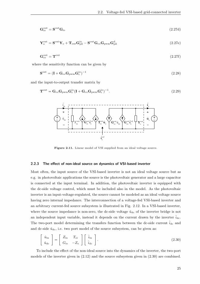
2.2.3 The effect of non-ideal source on dynamics of VSI-based inverter
Most often, the input source of the VSI-based inverter is not an ideal voltage source but as
e.g. in photovoltaic applications the source is the photovoltaic generator and a large capacitor
is connected at the input terminal. In addition, the photovoltaic inverter is equipped with
the dc-side voltage control, which must be included also in the model. As the photovoltaic
inverter is an input-voltage-regulated, the source cannot be modeled as an ideal voltage source
having zero internal impedance. The interconnection of a voltage-fed VSI-based inverter and
an arbitrary current-fed source subsystem is illustrated in Fig. 2.12. In a VSI-based inverter,
where the source impedance is non-zero, the dc-side voltage udc of the inverter bridge is not
an independent input variable, instead it depends on the current drawn by the inverter idc.
The two-port model determining the transfers function between the dc-side current idc and
and dc-side udc, i.e. two port model of the source subsystem, can be given as:
[
uin
udc
]
=
[
Zin Toi
Gio −Zo
][
iin
idc
]
. (2.30)
To include the effect of the non-ideal source into the dynamics of the inverter, the two-port
models of the inverter given in (2.12) and the source subsystem given in (2.30) are combined.
25

Chapter 2. Dynamic characterization of voltage-source inverters
inY
ciˆG d
oi oˆT u
d
io dcuG
coˆG d
oY
ou
oi
dcu
dci
oZ
io inˆG i
VF VSI-based inverterini
inu
oi dcˆT i
inZ
Dc-side subcircuit
Figure 2.12. Linear model of the output current-controlled VSI supplied from a non-ideal source.
The two-port model characterizing the interconnected system, i.e. the source-affected VSI-
based inverter, can be given by
[
uin
io
]
=
[
ZSin TS
oi GSci
GSio −YS
o GSco
]
iin
uo
d
(2.31)
where the superscript ’S’ refers to the transfer functions including the effect of the non-ideal
source. The transfer functions including the source-effect in (2.31) can be given by
ZSin = Zdc
in + T dcoi
Y vsiin Gdc
io
1 + Zdco Y vsi
in
(2.32a)
TSoi = T dc
oi1
1 + Y vsiin Zdc
o
Tvsioi (2.32b)
GSci = T dc
oi1
1 + Y vsiin Zdc
o
Gvsici (2.32c)
GSio = Gvsi
ioGdc
io
1 + Zdco Y vsi
in
(2.32d)
YSo = Yvsi
o +Gvsiio
Zdco
1 + Zdco Y vsi
in
Tvsioi (2.32e)
GSco = Gvsi
co −Gvsiio
Zdco
1 + Zdco Y vsi
in
Gvsici , (2.32f)
where superscript ’dc’ and ’vsi’ are used to denote the transfer functions of the source sub-
system and the VSI, respectively.
Moreover, in the interconnected system the dc-link voltage is no longer the input variable
of the system. As a consequence, the new system input variables can be used to regulate the
dc-link voltage, i.e. the dc-link voltage can be taken as a feedback variable. The dynamics
associated to the dc-link voltage can be given by[
udc
]
=[
GSidc GS
odc GScdc
] [
iph uo d
]T
, (2.33)
where
GSidc =
1
1 + Zdco Y vsi
in
Gdcio (2.34a)
26

2.3. VSI-based single and two-stage photovoltaic inverters
GSodc = −
Zdco
1 + Zdco Y vsi
in
Tvsioi (2.34b)
GScdc = −
Zdco
1 + Zdco Y vsi
in
Gvsici (2.34c)
The equations presented above to compute the source-affected transfer functions are valid
for an inverter operating at open loop and under output-current control, i.e. for models given
in (2.12) and (2.26), respectively.
2.3 VSI-based single and two-stage photovoltaic inverters
It should be noted that the following modeling method for the photovoltaic VSI is not the most
convenient to the represent its dynamics (Puukko and Suntio; 2012). However, it provides a
tool to compare the characteristics of the Z-source inverter and the VSI-based inverter, as a
part of the power stage is the same in both of the converters.
2.3.1 Single-stage VSI-based photovoltaic inverter
The single-stage photovoltaic inverter is supplied from a parallel connection of a photovoltaic
generator and the input capacitor (also known as the dc-link capacitor). The source subsystem
that will take into an account the effect of the capacitor and the photovoltaic generator
according to Fig. 2.13 can be represented as:
[
upv
udc
]
=
[
Zeq −Zeq
Zeq −Zeq
][
iph
idc
]
, (2.35)
where
Zeq =1
Ypv + YCdc= rpv||ZCdc =
rpv(
1sCdc
+ rCdc
)
rpv + 1sCdc
+ rCdc
=rpv (1 + sCdcrCdc)
sCdc(rpv + rCdc) + 1. (2.36)
The effect of the source subsystem can be included using the source affected model given
in (2.31). However, since the current control is always required in VSI-based inverter, the
source effect can be included directly to the output-current controlled inverter.
CdcY
dci
dcu
out
inY
out ref
ci oˆG i
out
oi oˆT u
ref
oi
out
oi dcuG
out ref
co oˆG i
out
oY
ou
oi
pvu
phi
pvY
pvi
VF VSI-based inverterDc cap.PVG
Figure 2.13. Linear model of the output current-controlled VSI supplied from a photovoltaic generator.
27

Chapter 2. Dynamic characterization of voltage-source inverters
out
inY
out
oiT
out
ioG
out
o-Y
out
coG
out
ciG
ref
oi
phi
ou
eqZ
dci
oi
dcu
Figure 2.14. Including the effect of non-ideal source on current-controlled VSI-based inverter model.
Dashed area represent the dynamics of the output-current-controlled inverter (see Fig. 2.10). An internal
feedback loop is formed, where the loop gain equals ZeqYoutin .
The two-port model characterizing the source-affected current-controlled VSI-based in-
verter can be given by
[
udc
io
]
=
[
Y outSin ToutS
oi GoutSri
GoutSio −YoutS
o GoutSro
]
iph
uo
irefo
(2.37)
where the matrix elements are given explicitly in (2.38a) - (2.38f) and the superscript ’outS’
refers to the output-current-controlled transfer functions including the effect of the non-ideal
source.
ZoutSin =
Zeq
1 + ZeqY vsi-outin
(2.38a)
ToutSoi = −
Zeq
1 + ZeqY vsi-outin
Tvsi-outoi (2.38b)
GoutSri = −
Zeq
1 + ZeqY vsi-outin
Gvsi-outri (2.38c)
GoutSio =
Zeq
1 + ZeqY vsi-outin
Gvsi-outio (2.38d)
YoutSo = Yvsi-out
o +Zeq
1 + ZeqY vsi-outin
Gvsi-outio Tvsi-out
oi (2.38e)
GoutSro = Gvsi-out
ro −Zeq
1 + ZeqY vsi-outin
Gvsi-outio Gvsi-out
ri (2.38f)
The model given in (2.37) includes the effect of the non-ideal source and the current control.
To include the input voltage control, the model of the output current controlled voltage-fed
VSI-based inverter given in (2.26) is repeated in (2.39), with the exception that the small-
signal value of the quadrature component of the output current reference is set to zero, since
28
2.3. VSI-based single and two-stage photovoltaic inverters
according to Fig. 2.4, it is not affected by the dc-link-voltage controller. The model of the
output-current controlled converter can be thus given by
[
udc
io
]
=
[
Y outSin ToutS
oi GoutSri-d
GoutSio −YoutS
o GoutSro-d
]
iph
uo
irefo-d
(2.39)
where the control-to-output transfer function matrix equals
GoutSro-d =
[
Goutro-d Gout
ro-dq
]T
. (2.40)
outS
inZ
outS
oiT
outS
ioG
outS
o-Y
outS
ro-dG
outS
ri-dG
ref
o-di
dcu
oi
phi
ou
udc
seG
udc
cG
ref
dcu
Figure 2.15. Control-block diagram of a dc-link voltage control.
The model is then used to include the effect of the dc-link-voltage control. Under the
dc-link-voltage control, the converter direct-channel-current reference is given by the voltage
controller according to
irefo-d = Gudcc
(
urefdc − udc
)
, (2.41)
where Gudcc is the dc-link-voltage controller transfer function. Unity measurement gain is
assumed.
Finally, the closed-loop transfer function including the effect of the dc-link-voltage control
is found by substituting the current reference in (2.39) by the the output of the dc-link-voltage
controller given in (2.41). The resulting closed-loop transfer functions of the system can be
given by
[
udc
io
]
=
[
Y inoutSin TinoutS
oi GinoutSri
GinoutSio −YinoutS
o GinoutSro
]
iph
uo
urefdc
, (2.42)
where
Z inoutSin =
1
1 +GoutSri-d Gudc
c
ZoutSin (2.43a)
T inoutSoi =
1
1 +GoutSri-d Gudc
c
ToutSoi (2.43b)
GinoutSri =
GoutSri-d Gudc
c
1 +GoutSri-d Guin
c
(2.43c)
29
Chapter 2. Dynamic characterization of voltage-source inverters
GinoutSio = GoutS
io −GoutSro-d G
udcc
1
1 +GoutSri-d Gudc
c
ZoutSin (2.43d)
YinoutSo = YoutS
o +GoutSro-d G
udcc
1
1 +GoutSri-d Gudc
c
ToutSoi (2.43e)
GinoutSro = GoutS
ro-d Gudcc
1
1 +GoutSri-d Gudc
c
. (2.43f)
The model given in (4.17) can be used to compute all the transfer functions of the VSI-
based inverter operating at closed loop. The model produces the same results as the models
that has been previously published e.g. in (Puukko and Suntio; 2012) and (Messo et al.; 2015)
but it is formulated slightly differently.
2.3.2 Two-stage VSI-based photovoltaic inverter
The method to derive transfer functions of the two-stage VSI-based inverter is basically the
same as in case of VSI-based inverter. The inverter dc-side subsystem is now the boost-stage
fed by the photovoltaic generator. The circuit structure using the two-port models is shown
in Fig. 2.16. When the boost-stage is operated at open loop, the control variable in Fig. 2.16
is the duty ratio of the boost-stage. In closed-loop operation, the control variable is the input
voltage reference. The effect of the source subsystem to the inverter dynamics is now dictated
by the output impedance of the voltage-boosting dc-dc stage and the dc-link capacitor.
dci
dcu
out
inY
out ref
ci oˆG i
out
oi oˆT u
ref
oi
out
oi dcuG
out ref
co oiG out
oY
ou
oi
oi
dcupv
u
pvi
inZ
ciˆG c
oi dcˆT u
io pvˆG i
coˆG c
oY
c
phi
pvY
CdcY
Voltage-boosting-converter Output-current controlledVSI-based inverterDc cap.PVG
Figure 2.16. Linear model of the output current-controlled VSI supplied from a voltage-boosting dc-dc
converter.
The effect of the nonzero source impedance on inverter dynamics can be included in the
model by combining the H-parameter model of the voltage-boosting converter, the impedance
of the dc-link capacitor, and the Y-parameter model of the VSI as illustrated in Fig. 2.16.
The two-port model of the interconnected system can be given by
[
upv
io
]
=
[
ZoutSin ToutS
oi GoutSri GoutS
ci
GoutSio −YoutS
o GoutSro GoutS
co
]
iph
uo
irefo
c
, (2.44)
where
ZoutSin = ZS
in +Zeq
1 + ZeqY vsi-outin
GSioT
Soi (2.45a)
30

2.3. VSI-based single and two-stage photovoltaic inverters
T outSoi = −T S
oiZeq
1 + ZeqY vsi-outin
Tvsi-outoi (2.45b)
GoutSri = −T S
oiZeq
1 + ZeqY vsi-outin
Gvsi-outci (2.45c)
GoutSci = GS
ci − T Soi
Zeq
1 + ZeqY vsi-outin
GSco (2.45d)
GoutSio =
Zeq
1 + ZeqY vsi-outin
GSioG
vsi-outio (2.45e)
Y outSo = Yvsi-out
o +Zeq
1 + ZeqY vsi-outin
Gvsi-outio Tvsi-out
oi (2.45f)
GoutSro = Gvsi-out
co −Zeq
1 + ZeqY vsi-outin
Gvsi-outio Gvsi-out
ci (2.45g)
GoutSco =
Zeq
1 + ZeqY vsi-outin
GScoG
vsi-outio (2.45h)
Usually, as in single-stage inverter, the dc-link voltage is taken as a feedback variable. The
dynamics of the dc-link voltage can be given by
[
udc
]
=[
GoutSidc GoutS
odc GoutSrdc GoutS
cdc
] [
iph uo irefo c]T
, (2.46)
where
GoutSidc =
Zeq
1 + ZeqY vsi-outin
GSio (2.47a)
GoutSodc = −
Zeq
1 + ZeqY vsi-outin
Tvsi-outoi (2.47b)
GoutSrdc = −
Zeq
1 + ZeqY vsi-outin
Gvsi-outci (2.47c)
GoutScdc =
Zeq
1 + ZeqY vsi-outin
GSco. (2.47d)
In (2.45a) - (2.47d), the superscript ’S’ denotes the source-affected transfer functions of
the boost-stage, superscript ’vsi-out’ the output-current-controlled VSI, and the equivalent
source impedance equals
Zeq =1
Y So + YCdc
, (2.48)
where Y So is the output admittance of the boost-stage. The dc-link-voltage controller can then
be included in the model using the same procedure as in the single-stage VSI-based inverter
presented in Section 2.3.1.
31

Chapter 2. Dynamic characterization of voltage-source inverters
2.4 Conclusions
This chapters proposed a method to characterize dynamics of a three-phase grid-connected
single and two-stage VSI-based inverters utilizing the model of a conventional voltage-source-
inverter. The models allow studying the operation of the inverter at open and closed loop
including the conventional synchronous-reference-frame current control. The advantage of the
presented modeling method is that the same voltage-fed VSI-based inverter model can be used
in analysis of single-stage PV inverter, two stage PV inverter, and Z-source inverter as will be
shown later.
32
3 DYNAMIC CHARACTERIZATION OF Z-SOURCE
INVERTERS
This chapter presents the small signal models suitable for analyzing the open-loop character-
istics of a three-phase voltage-fed and current-fed Z-source inverters (ZSI) in grid-connected
applications. In addition, a comparison between the results obtained from the voltage-fed and
the current-fed inverter are provided to justify the need of selecting correct two-port model
in the analysis.
3.1 Modeling of a voltage-fed and current-fed Z-source inverters
A voltage-fed three-phase grid-connected Z-source inverter is illustrated in Fig. 3.1. The
analysis of the ZSI can be carried out by using conventional averaging and linearization tech-
niques in synchronous reference frame. However, since the converter has very large number
of memory elements, the resulting transfer functions are very high order, which are tedious
or even impossible to analyze as such. As a consequence, the model for a voltage-fed and
current-fed ZSI is constructed by dividing the inverter into two subsystems, the impedance
network and the VSI-based inverter.
Lr L
o-(a,b,c)i
o-(a,b,c)u
L-(a,b,c)u
dc-equ
a
b
cn
L-(a,b,c)i
N
Ppi
cpS
bpS
apS
cnS
bnS
anS
C2u
L1u
L1i
L1r
1L
C2r
2C
1C
C1r
L2u
L2i
2L L2
r
C1u
C1iC2
i
ini
inu
Figure 3.1. Voltage-fed three-phase Z-source inverter.
As discussed e.g. in (Gajanayake et al.; 2007) and (Li et al.; 2013), the impedance network
and the inverter stage can be analyzed as two separate subsystems, where the shoot-through
states are generated by an imaginary switch as shown in Fig. 3.2. As shown in Figs. 3.1 and
3.2, the impedance network and the VSI-based inverter parts are interconnected through the
33
Chapter 3. Dynamic characterization of Z-source inverters
equivalent dc-link. The current idc represent the current drawn by the inverter stage and the
voltage udc-eq represents the equivalent dc-link voltage seen by inverter stage. The dc-side
subsystem of the Z-source inverter is a voltage-fed impedance network. The output voltage of
the impedance network is dictated by the sum of impedance network capacitor voltages and the
input voltage, i.e. the output terminal is a voltage-type, and thus the voltage-fed impedance
network must be analyzed using the voltage-to-voltage conversion scheme. Similar analysis is
valid for a current-fed impedance network, which has to be analyzed as a current-to-voltage
conversion scheme as will be shown later.
dc-equ
dci
C2u
L1u
L1i
L1r
1L
C2r
2C
1C
C1r
L2u
L2i
2L
L2r
C1u
C1iC2
i
piD
stS
4S
1S
ini
inu
5S
2S
6S
3S
o-(a,b,c)i
o-(a,b,c)u
a
b
cn
L-(a,b,c)i
L-(a,b,c)u
Lr L
Figure 3.2. Equivalent circuit of a voltage-fed Z-source inverter. Dashed line illustrates the interface
between the impedance network and the inverter stage.
3.1.1 Modeling of a voltage-fed Z-source inverter impedance network
When the Z-source inverter operates in continuous conduction mode (CCM), the impedance
network may operate in three different states: a) shoot-through state, b) non-shoot-through
active state, and c) non-shoot-through zero state (Peng; 2003). During the shoot-through
state the switch in the equivalent circuit of the Fig. 3.3 is closed and during the non-shoot-
through states the switch is open. Undesired states will occur, if the inductor current or the
diode current falls to zero during the non-shoot-through state. In this thesis, only the CCM
operation is considered.
a) Shoot-through state
Shoot-through state forces the diode in circuit of Fig. 3.3 to reverse biased conditions. As
a result of the equivalent dc-link short-circuit, energy is transferred from impedance network
capacitors to impedance network inductors and at the same time the inverter must operate in
zero state. According to Fig. 3.3, the inductor voltages uL1 and uL2 during the shoot-through
state are
uL1 = uC2 − (rL1 + rC2)iL1 (3.1)
and
uL2 = uC1 − (rL2 + rC1)iL2, (3.2)
34

3.1. Modeling of a voltage-fed and current-fed Z-source inverters
dc-equ
dci
C2u
L1u
L1i
L1r
1L
C2r
2C
1C
C1r
L2u
L2i
2L
L2r
C1u
C1iC2
i
piD
stS
ini
inu
Figure 3.3. Equivalent circuit of a voltage-fed impedance network.
respectively. Correspondingly, since the diode is reverse biased, the capacitor currents are
iC1 = −iL2 (3.3)
and
iC2 = −iL1, (3.4)
respectively. The input current iin and the equivalent dc-link voltage udc-eq of the impedance
network are zero during the shoot-through state. In addition, since the inverter operates in
zero stage, the current idc must be zero.
b) Non-shoot-through active state
During the non-shoot-through active state, the inverter stage switch matrix of Fig. 3.2 op-
erates in one of the six active state. Now, the diode in the impedance network is forced to
forward bias conditions, and according to Fig. 3.3 the inductor voltages are
uL1 = uin − UD − rDiD − rL1iL1 − rC1iC1 − uC1 (3.5)
and
uL2 = uin − UD − rDiD − rL2iL2 − rC2iC2 − uC2, (3.6)
where UD is the diode forward voltage drop and rD diode on-state resistance. The diode
current and the capacitors currents in (3.5) and (3.6) can be computed as as a function of the
dc-link current and the inductor current, i.e.,
iC1 = iL1 − idc, (3.7)
iC2 = iL2 − idc, (3.8)
and
iD = iL1 + iC2 = iL1 + iL2 − idc. (3.9)
35

Chapter 3. Dynamic characterization of Z-source inverters
Inserting (3.7) - (3.9) to (3.5) and (3.6) yields
uL1 = uin − uC1 − UD − (rL1 + rC1 + rD)iL1 − rDiL2 + (rD + rC1)idc (3.10)
and
uL2 = uin − uC2 − UD − (rL2 + rC2 + rD)iL2 − rDiL1 + (rD + rC2)idc. (3.11)
During the non-shoot-through active state, energy is transferred from impedance network
to the inverter stage. The equivalent dc-link voltage supplying the inverter bridge can be
given by
udc = uC1 + uC2 − uin +UD − (rC1 + rC2 + rD)idc + (rC1 + rD)iL1 + (rC2 + rD)iL2 (3.12)
and the input current of the network by
iin = iD = iL1 + iL2 − idc. (3.13)
c) Non-shoot-through zero state
Equations representing the non-shoot-through zero state are the same as in the non-shoot-
through active state with the exception that the current flowing to inverter bridge switch
matrix idc is zero. When the inverter bridge current is zero, the inductor voltages and capacitor
currents can be given by
uL1 = uin − uC1 − UD − (rL1 + rC1 + rD)iL1 − rDiL2 (3.14a)
uL2 = uin − uC2 − UD − (rL2 + rC2 + rD)iL2 − rDiL1 (3.14b)
iC1 = iL1 (3.14c)
iC2 = iL2 (3.14d)
as well as the equivalent dc-link voltage and the input current by
udc = uC1 + uC2 − uin + UD + (rC1 + rD)iL1 + (rC2 + rD)iL2 (3.15a)
iin = iL1 + iL2. (3.15b)
36

3.1. Modeling of a voltage-fed and current-fed Z-source inverters
Averaging the operation of the voltage-fed impedance network
The average behavior of the impedance network is found by multiplying the equations de-
scribing the shoot-through state sub-circuit with the shoot-through duty cycle dst, and the
equations describing the operation during the non-shoot-through state with its complement d′st
(in continuous conduction mode, d′st = 1− dst). The average inductor voltages and capacitor
currents are proportional to the average inductor currents and capacitor voltages derivatives,
respectively, and the average model can be given by
L1d〈iL1〉
dt= dst〈uC2〉+ d′st〈uin〉 − d′st〈uC1〉 − d′stUD + (rD + rC1)〈idc〉
− (d′st(rL1 + rC1 + rD) + dst(rL1 + rC2))〈iL1〉 − d′strD〈iL2〉 (3.16a)
L2d〈iL2〉
dt= dst〈uC1〉+ d′st〈uin〉 − d′st〈uC2〉 − d′stUD + (rD + rC2)〈idc〉
− (d′st(rL2 + rC2 + rD) + dst(rL2 + rC1))〈iL2〉 − d′strD〈iL1〉 (3.16b)
C1d〈uC1〉
dt= d′st〈iL1〉 − dst〈iL2〉 − 〈idc〉, (3.16c)
C2d〈uC2〉
dt= −dst〈iL1〉+ d′st〈iL2〉 − 〈idc〉, (3.16d)
The average of the equivalent dc-link voltage may be written as
〈udc〉 = 〈uC1〉+ 〈uC2〉 − 〈uin〉+ UD − (rC1 + rC2 + rD) 〈idc〉
(rC1 + rD) 〈iL1〉 + (rC2 + rD) 〈iL2〉 (3.17)
and the average input current of the impedance network as
〈iin〉 = d′st〈iL1〉+ d′st〈iL2〉 − 〈idc〉. (3.18)
Steady state operating point
The steady-state operating point of the converter can be solved by setting the time derivatives
of the average model in (3.16a) - (3.18) to zero. The steady state values denoted by the
uppercase letters of the impedance network currents as a function of the input current are
IL1 = IL2 = Iin, Idc = (1− 2Dst)Iin. (3.19)
A reasonable simplification of the circuit is that the impedance network capacitor and
inductor ESRs are equal, i.e. rC1 = rC2 and rL1 = rL2. With this assumption, the shoot-
through duty cycle of the converter as a function of the input voltage, input current, and the
impedance network capacitor voltage equals
Dst =UCz − Uin + UD + (rD + rL1)Iin2UCz − Upv + UD − 2rC1Iin
, (3.20)
37
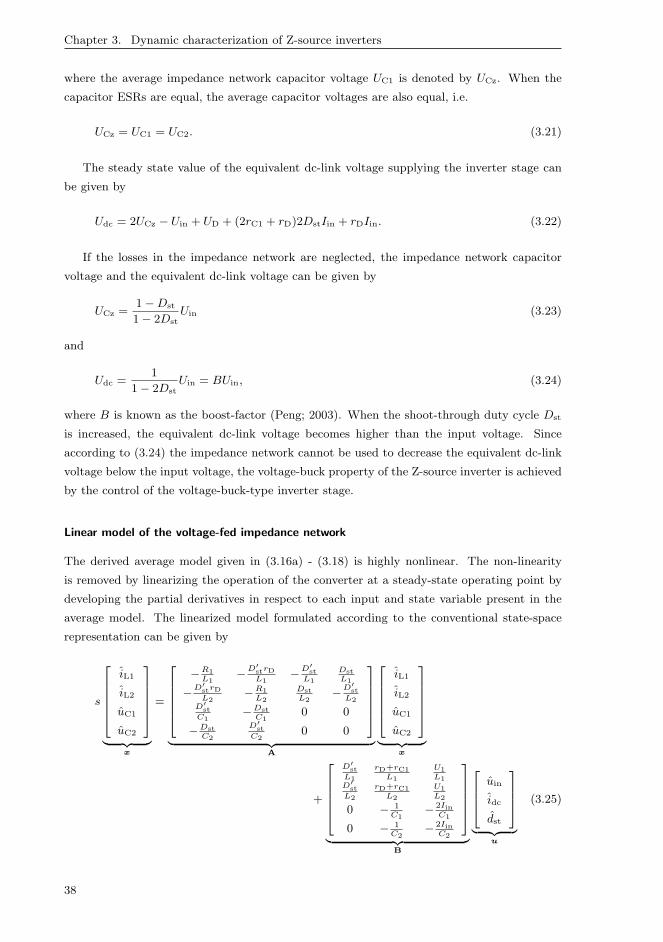
Chapter 3. Dynamic characterization of Z-source inverters
where the average impedance network capacitor voltage UC1 is denoted by UCz. When the
capacitor ESRs are equal, the average capacitor voltages are also equal, i.e.
UCz = UC1 = UC2. (3.21)
The steady state value of the equivalent dc-link voltage supplying the inverter stage can
be given by
Udc = 2UCz − Uin + UD + (2rC1 + rD)2DstIin + rDIin. (3.22)
If the losses in the impedance network are neglected, the impedance network capacitor
voltage and the equivalent dc-link voltage can be given by
UCz =1−Dst
1− 2DstUin (3.23)
and
Udc =1
1− 2DstUin = BUin, (3.24)
where B is known as the boost-factor (Peng; 2003). When the shoot-through duty cycle Dst
is increased, the equivalent dc-link voltage becomes higher than the input voltage. Since
according to (3.24) the impedance network cannot be used to decrease the equivalent dc-link
voltage below the input voltage, the voltage-buck property of the Z-source inverter is achieved
by the control of the voltage-buck-type inverter stage.
Linear model of the voltage-fed impedance network
The derived average model given in (3.16a) - (3.18) is highly nonlinear. The non-linearity
is removed by linearizing the operation of the converter at a steady-state operating point by
developing the partial derivatives in respect to each input and state variable present in the
average model. The linearized model formulated according to the conventional state-space
representation can be given by
s
iL1
iL2
uC1
uC2
︸ ︷︷ ︸x
=
−R1
L1−
D′
strD
L1−
D′
st
L1
Dst
L1
−D
′
strD
L2−R1
L2
Dst
L2−
D′
st
L2D
′
st
C1−Dst
C10 0
−Dst
C2
D′
st
C20 0
︸ ︷︷ ︸A
iL1
iL2
uC1
uC2
︸ ︷︷ ︸x
+
D′
st
L1
rD+rC1
L1
U1
L1D
′
st
L2
rD+rC1
L2
U1
L2
0 − 1C1
− 2IinC1
0 − 1C2
− 2IinC2
︸ ︷︷ ︸B
uin
idc
dst
︸ ︷︷ ︸u
(3.25)
38
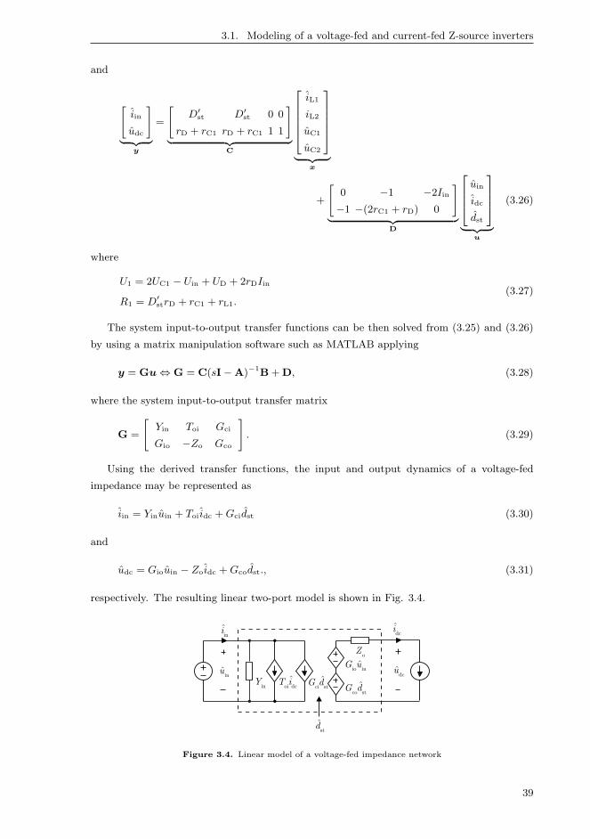
3.1. Modeling of a voltage-fed and current-fed Z-source inverters
and
[
iin
udc
]
︸ ︷︷ ︸y
=
[
D′st D′
st 0 0
rD + rC1 rD + rC1 1 1
]
︸ ︷︷ ︸C
iL1
iL2
uC1
uC2
︸ ︷︷ ︸x
+
[
0 −1 −2Iin
−1 −(2rC1 + rD) 0
]
︸ ︷︷ ︸D
uin
idc
dst
︸ ︷︷ ︸u
(3.26)
where
U1 = 2UC1 − Uin + UD + 2rDIin
R1 = D′strD + rC1 + rL1.
(3.27)
The system input-to-output transfer functions can be then solved from (3.25) and (3.26)
by using a matrix manipulation software such as MATLAB applying
y = Gu ⇔ G = C(sI−A)−1B+D, (3.28)
where the system input-to-output transfer matrix
G =
[
Yin Toi Gci
Gio −Zo Gco
]
. (3.29)
Using the derived transfer functions, the input and output dynamics of a voltage-fed
impedance may be represented as
iin = Yinuin + Toi idc +Gcidst (3.30)
and
udc = Giouin − Zo idc +Gcodst., (3.31)
respectively. The resulting linear two-port model is shown in Fig. 3.4.
dcu
dci
oZ
co stˆG d
io inˆG u
std
ini
inu
ci stˆG d
oi dcˆT i
inY
Figure 3.4. Linear model of a voltage-fed impedance network
39

Chapter 3. Dynamic characterization of Z-source inverters
If the parasitic components are neglected and the impedance network is assumed to be
ideal, the set of transfer functions describing the open-loop dynamics of the voltage-fed
impedance network can be given by:
Yin =1
∆vf
2D′2sts
L1(3.32a)
Toi =
(1
∆vf
2(1− 2Dst)D′st
C1L1− 1
)
(3.32b)
Gci = −1
∆vf2D′
st2IinL1C1
(
1−s
ωzero-in
)
− 2Iin (3.32c)
Gio =
(1
∆vf
2(1− 2Dst)D′st
L1C1− 1
)
(3.32d)
Zo =1
∆vf
2s
C1(3.32e)
Gco =1
∆vf
2(1− 2Dst)Udc
L1C1
(
1−s
ωzero-out
)
, (3.32f)
where the right-half-plane zeros associated with the control-to-input and the control-to-output
transfer functions are
ωzero-in =2Iin
UdcC1, ωzero-out =
(1− 2Dst)Udc
2IinL1, (3.33)
respectively, and the characteristic polynomial of a voltage-fed system is
∆vf = s2 + ω2res, (3.34)
where
ωres =
√
1− 4DstD′st
L1C1. (3.35)
According to (3.32a) - (3.35), the ideal impedance network is a second-order system, having
an operating-point-dependent resonant frequency and right-half-plane zeros in the control
dynamics.
In Z-source inverter, the inductor current and/or the capacitor voltage may be also taken
as a feedback variable. To analyze the dynamics associated with the state variables, the
input-to-state transfer functions are found by solving the state-transition matrix Φ as shown
in (3.36).
x = Φu ⇔ Φ = (sI−A)−1B, (3.36)
where
Φ =
GiL1 GoL1 GcL1
GiL2 GoL2 GcL2
GiC1 GoC1 GcC1
GiC2 GoC2 GcC2
. (3.37)
40
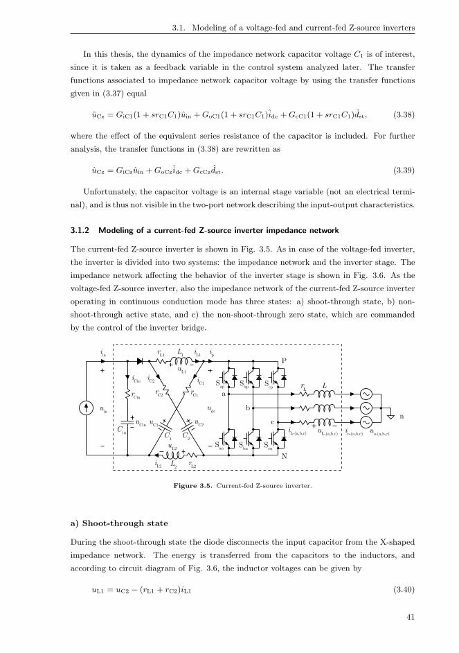
3.1. Modeling of a voltage-fed and current-fed Z-source inverters
In this thesis, the dynamics of the impedance network capacitor voltage C1 is of interest,
since it is taken as a feedback variable in the control system analyzed later. The transfer
functions associated to impedance network capacitor voltage by using the transfer functions
given in (3.37) equal
uCz = GiC1(1 + srC1C1)uin +GoC1(1 + srC1C1)idc +GcC1(1 + srC1C1)dst, (3.38)
where the effect of the equivalent series resistance of the capacitor is included. For further
analysis, the transfer functions in (3.38) are rewritten as
uCz = GiCzuin +GoCz idc +GcCzdst. (3.39)
Unfortunately, the capacitor voltage is an internal stage variable (not an electrical termi-
nal), and is thus not visible in the two-port network describing the input-output characteristics.
3.1.2 Modeling of a current-fed Z-source inverter impedance network
The current-fed Z-source inverter is shown in Fig. 3.5. As in case of the voltage-fed inverter,
the inverter is divided into two systems: the impedance network and the inverter stage. The
impedance network affecting the behavior of the inverter stage is shown in Fig. 3.6. As the
voltage-fed Z-source inverter, also the impedance network of the current-fed Z-source inverter
operating in continuous conduction mode has three states: a) shoot-through state, b) non-
shoot-through active state, and c) the non-shoot-through zero state, which are commanded
by the control of the inverter bridge.
Lr L
o-(a,b,c)i
o-(a,b,c)u
L-(a,b,c)u
dcu
a
b
cn
L-(a,b,c)i
N
Ppi
cpS
bpS
apS
cnS
bnS
anS
ini
Cinr
inC
Cinu
inu
C2u
L1u
L1i
L1r
1L
C2r
2C
1C
C1r
L2u
L2i
2L L2
r
C1u
Cini
C1iC2
i
Figure 3.5. Current-fed Z-source inverter.
a) Shoot-through state
During the shoot-through state the diode disconnects the input capacitor from the X-shaped
impedance network. The energy is transferred from the capacitors to the inductors, and
according to circuit diagram of Fig. 3.6, the inductor voltages can be given by
uL1 = uC2 − (rL1 + rC2)iL1 (3.40)
41

Chapter 3. Dynamic characterization of Z-source inverters
dc-equ
ini
Cinr
inC
Cinu
inu
C2u
L1u
L1i
L1r
1L
C2r
2C
1C
C1r
L2u
L2i
2L
L2r
C1u
Cini
C1iC2
i
piD
stS
dci
Figure 3.6. Current-fed impedance network
and
uL2 = uC1 − (rL2 + rC1)iL2. (3.41)
Correspondingly, the impedance network capacitors currents can be given by
iC1 = −iL2 (3.42)
and
iC2 = −iL1. (3.43)
The current-fed impedance network has one additional memory element compared to the
voltage-fed impedance network, the input capacitor. Since the diode is reverse biased, the
current of the input capacitor equals the input current of the converter, i.e.
iin = iCin = CinduCin
dt. (3.44)
The input voltage of the converter during the shoot-through state is
uin = uCin + rCiniin. (3.45)
b) Non-shoot-through active state
During the active state, the diode in the impedance network is forward biased, and according
to Fig. 3.6 the inductor voltages can be given by
uL1 = uin − UD − rDiD − rL1iL1 − rC1iC1 − uC1 (3.46)
and
uL2 = uin − UD − rDiD − rL2iL2 − rC2iC2 − uC2, (3.47)
where UD is the diode forward voltage drop and rD diode on-state resistance. The capacitor
currents and diode current in (3.46) and (3.47) can be given by
iC1 = iL1 − idc, (3.48)
42

3.1. Modeling of a voltage-fed and current-fed Z-source inverters
iC2 = iL2 − idc (3.49)
and
iD = iL1 + iC2 = iL1 + iL2 − idc. (3.50)
During the non-shoot-through state, the input voltage of the impedance network can be
given by
uin = uCin + rCiniin − rCiniL1 − rCiniL2 + rCinidc. (3.51)
Inserting (3.48) - (3.50) and (3.51) into (3.46) and (3.47) yields
uL1 = uCin − uC1 − UD − (rL1 + rC1 + rD + rCin)iL1 − (rD + rCin)iL2
+ (rD + rC1 + rCin)idc + rCiniin (3.52)
and
uL2 = uCin − uC2 − UD − (rL2 + rC2 + rD + rCin)iL2 − (rD + rCin)iL1
+ (rD + rC2 + rCin)idc + rCiniin. (3.53)
During the non-shoot-through state, the impedance network capacitor and input capacitor
currents are
iC1 = iL1 − idc, (3.54)
iC2 = iL2 − idc (3.55)
and
iCin = iin − iL1 − iL2 + idc. (3.56)
Finally, the equivalent dc-link voltage during the non-shoot-through state can be given by
udc = uC1 + uC2 − uCin + UD + (rC1 + rD + rCin)iL1 + (rC2 + rD + rCin)iL2
− (rC1 + rC2 + rD + rCin)idc − rCiniin. (3.57)
c) Non-shoot-through zero state
The equations corresponding to the non-shoot-through zero stage and given in (3.58a) - (3.58g)
are the same as the equations of the non-shoot-through active state given above with the
exception that the output current of the network is zero.
uL1 = uCin − uC1 − UD − (rL1 + rC1 + rD + rCin)iL1 − (rD + rCin)iL2
+ (rD + rC1 + rCin)idc + rCiniin (3.58a)
43

Chapter 3. Dynamic characterization of Z-source inverters
uL2 = uCin − uC2 − UD − (rL2 + rC2 + rD + rCin)iL2 − (rD + rCin)iL1
+ (rD + rC2 + rCin)idc + rCiniin. (3.58b)
iC1 = iL1 (3.58c)
iC2 = iL2 (3.58d)
iCin = iin − iL1 − iL2 (3.58e)
uin = uCin + rCiniin − rCiniL1 − rCiniL2 (3.58f)
udc = uC1 + uC2 − uCin + UD + (rC1 + rD + rCin)iL1 + (rC2 + rD + rCin)iL2
− rCiniin. (3.58g)
Averaging the operation of the current-fed impedance network
As in voltage-fed impedance network, the average behavior of the network is found by mul-
tiplying the equations describing the shoot-through state sub circuit with the shoot-through
duty cycle dst, and the equations describing the operation during the non-shoot-through state
with its complement d′st. In continuous conduction mode, d′st = 1−dst, and the average model
can be given by
L1d〈iL1〉
dt= dst〈uC2〉+d′st〈uCin〉−d′st〈uC1〉−d′stUD+(rD+ rC1+ rCin)〈idc〉+d′strCin〈iin〉
− (d′st(rL1 + rC1 + rD + rCin) + dst(rL1 + rC2))〈iL1〉 − d′st(rD + rCin)〈iL2〉 (3.59a)
L2d〈iL2〉
dt= dst〈uC1〉+d′st〈uCin〉−d′st〈uC2〉−d′stUD+(rD+ rC2+ rCin)〈idc〉+d′strCin〈iin〉
− (d′st(rL2 + rC2 + rD + rCin) + dst(rL2 + rC1))〈iL2〉 − d′st(rD + rCin)〈iL1〉 (3.59b)
C1d〈uC1〉
dt= d′st〈iL1〉 − dst〈iL2〉 − 〈idc〉 (3.59c)
C2d〈uC2〉
dt= −dst〈iL1〉+ d′st〈iL2〉 − 〈idc〉 (3.59d)
Cind〈uCin〉
dt= 〈iin〉 − d′st〈iL1〉 − d′st〈iL2〉+ 〈idc〉. (3.59e)
Using the same procedure, the average behavior of the input and the output terminal can
be given by
〈uin〉 = rCin〈iin〉+ 〈uCin〉 − rCind′st〈iL1〉 − rCind
′st〈iL2〉+ rCin〈idc〉 (3.60a)
〈udc〉 = 〈uC1〉+ 〈uC2〉 − 〈uCin〉+ UD − (rC1 + rC2 + rD + rCin) 〈idc〉
+ (rC1 + rD + rCin) 〈iL1〉+ (rC2 + rD + rCin) 〈iL2〉 − rCin〈iin〉. (3.60b)
44
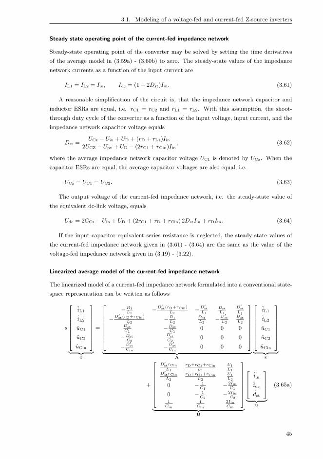
3.1. Modeling of a voltage-fed and current-fed Z-source inverters
Steady state operating point of the current-fed impedance network
Steady-state operating point of the converter may be solved by setting the time derivatives
of the average model in (3.59a) - (3.60b) to zero. The steady-state values of the impedance
network currents as a function of the input current are
IL1 = IL2 = Iin, Idc = (1− 2Dst)Iin. (3.61)
A reasonable simplification of the circuit is, that the impedance network capacitor and
inductor ESRs are equal, i.e. rC1 = rC2 and rL1 = rL2. With this assumption, the shoot-
through duty cycle of the converter as a function of the input voltage, input current, and the
impedance network capacitor voltage equals
Dst =UCz − Uin + UD + (rD + rL1)Iin
2UCZ − Upv + UD − (2rC1 + rCin)Iin, (3.62)
where the average impedance network capacitor voltage UC1 is denoted by UCz. When the
capacitor ESRs are equal, the average capacitor voltages are also equal, i.e.
UCz = UC1 = UC2. (3.63)
The output voltage of the current-fed impedance network, i.e. the steady-state value of
the equivalent dc-link voltage, equals
Udc = 2CCz − Uin + UD + (2rC1 + rD + rCin) 2DstIin + rDIin. (3.64)
If the input capacitor equivalent series resistance is neglected, the steady state values of
the current-fed impedance network given in (3.61) - (3.64) are the same as the value of the
voltage-fed impedance network given in (3.19) - (3.22).
Linearized average model of the current-fed impedance network
The linearized model of a current-fed impedance network formulated into a conventional state-
space representation can be written as follows
s
iL1
iL2
uC1
uC2
uCin
︸ ︷︷ ︸x
=
−R1
L1−
D′
st(rD+rCin)
L1−
D′
st
L1
Dst
L1
D′
st
L1
−D
′
st(rD+rCin)
L2−R1
L2
Dst
L2−
D′
st
L2
D′
st
L2D
′
st
C1−Dst
C10 0 0
−Dst
C2
D′
st
C20 0 0
−D
′
st
Cin−
D′
st
Cin0 0 0
︸ ︷︷ ︸A
iL1
iL2
uC1
uC2
uCin
︸ ︷︷ ︸x
+
D′
strCin
L1
rD+rC1+rCin
L1
U1
L1D
′
strCin
L2
rD+rC1+rCin
L2
U1
L2
0 − 1C1
− 2IinC1
0 − 1C2
− 2IinC2
1Cin
1Cin
2IinCin
︸ ︷︷ ︸B
iin
idc
dst
︸ ︷︷ ︸u
(3.65a)
45

Chapter 3. Dynamic characterization of Z-source inverters
and
[
uin
udc
]
︸ ︷︷ ︸y
=
[
−D′strCin −D′
strCin 0 0 1
rD + rC1 + rCin rD + rC1 + rCin 1 1 −1
]
︸ ︷︷ ︸C
iL1
iL2
uC1
uC2
uCin
︸ ︷︷ ︸x
+
[
rCin rCin 2rCinIin
−rCin −(2rC1 + rD + rCin) 0
]
︸ ︷︷ ︸D
iin
idc
dst
︸ ︷︷ ︸u
, (3.65b)
where
U1 = 2UC1 − Uin + UD + (2rD + rCin)Iin
R1 = D′st(rD + rCin) + rC1 + rL1.
(3.66)
The state-space model is then used to solve the transfer function matrix given in (3.67) of
the current-fed impedance network.
G =
[
Zin Toi Gci
Gio −Zo Gco
]
. (3.67)
Using the derived transfer functions, the input and the output dynamics may be represented
as follows:
uin = Zin iin + Toi idc +Gcidst (3.68)
and
udc = Gio iin − Zo idc +Gcodst, (3.69)
which can be also depicted using the linear two-port shown in Fig. 3.15.
ini
inu
dcu
dci
oZ
co stˆG d
io inˆG i
ci stˆG d
oi dcˆT i
inZ
std
Figure 3.7. Linear model of a current-fed impedance network
If the parasitic components are neglected and the impedance network is assumed to be
ideal, the set of transfer functions describing the open-loop dynamics of the current-fed
impedance network can be written as follows:
Zin =1
∆cf
(
s2 +(2Dst − 1)2
L1C1
)1
Cin(3.70a)
46

3.1. Modeling of a voltage-fed and current-fed Z-source inverters
Toi =1
∆cf
(s2L1C1 + (2Dst − 1)
L1C1Cin
)
(3.70b)
Gci =1
∆cf
2
CinL1C1
(s2IinL1C1 − sD′
stUdcC1 + (2Dst − 1)Iin)
(3.70c)
Gio = −1
∆cf
(s2L1C1 + (2Dst − 1)
L1C1Cin
)
(3.70d)
Zo =1
∆cf
(s2(2L1Cin + L1C1) + (2Dst − 1) + 2D′
st
L1C1Cin
)
(3.70e)
Gco = −1
∆cf
1
L1C1Cin
(
(4Cin + L1C1)Iins2
+ (D′stC1 − 2(1− 2Dst)Cin)Udcs+ ((2Dst − 1)− 4D′
st)Iin
)
, (3.70f)
where the characteristic polynomial of the system equals
∆cf = s
(
s2 +2D′2
stC1 + Cin(2Dst − 1)2
CinC1L1
)
. (3.71)
The dynamics of the ideal current-fed impedance network are third order, and the location
of the resonance depends on the operating point of the inverter.
As in the voltage-fed impedance network, the inductor current and/or the capacitor voltage
may be also taken as a feedback variable. The input-to-state transfer functions are found by
solving the state-transition matrix of the current-fed system and including the effect of the
equivalent series resistances as shown previously in (3.36) - (3.39).
3.1.3 Comparison of current-fed and voltage-fed ZSI dynamic characteristics
To compare the characteristics of a voltage-fed and a current-fed Z-source inverter, first a
method to include the effect of the impedance network to the inverter dynamics must be
derived.
Voltage-fed Z-source inverter
The voltage-fed impedance network model can be combined with the model of the voltage-fed
VSI-based inverter model as shown in Fig. 3.8.
When the source subsystem (the impedance network) and the load subsystem (the VSI-
based inverter) are interconnected, the new system input variables are the input current of
the impedance network iin, output voltage of the inverter stage (i.e. the grid voltage) uo,
shoot-through duty cycle of the impedance network dst, and duty ratio of the inverter stage
d. The dc-link current idc and the dc-link udc are the internal state-variables (intermediate
variables) of the system.
[
iin
io
]
=
[
Y vf-zsiin Tvf-zsi
oi Gvf-zsici Gvf-zsi
sti
Gvf-zsiio −Yvf-zsi
o Gvf-zsico Gvf-zsi
sto
]
uin
uo
d
dst
, (3.72)
47
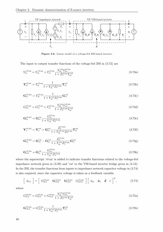
Chapter 3. Dynamic characterization of Z-source inverters
inY
ciˆG d
oi oˆT u
d
io dcuG
coˆG d
oY
ou
oi
ini
inu
dcu
dci
oZ
co stˆG d
io inˆG u
ci stˆG d
oi dcˆT i
inY
std
VF VSI-based inverterVF impedance network
Figure 3.8. Linear model of a voltage-fed ZSI-based inverter.
The input to output transfer functions of the voltage-fed ZSI in (3.72) are
Y vf-zsiin = Y vf-zn
in + T vf-znoi
Y vsiin Gvf-zn
io
1 + Zvf-zno Y vsi
in
(3.73a)
Tvf-zsioi = T vf-zn
oi1
1 + Y vsiin Zvf-zn
o
Tvsioi (3.73b)
Gvf-zsici = T vf-zn
oi1
1 + Y vsiin Zvf-zn
o
Gvsici (3.73c)
Gvf-zsisti = Gvf-zn
ci + T vf-znoi
Y vsiin Gvf-zn
co
1 + Zvf-zno Y vsi
in
(3.73d)
Gvf-zsiio = Gvsi
ioGvf-zn
io
1 + Y vsiin Zvf-zn
o
(3.73e)
Yvf-zsio = Yvsi
o +Gvsiio
Zvf-zno
1 + Y vf-vsiin Zvf-zn
o
Tvsioi (3.73f)
Gvf-zsico = Gvsi
co −Gvsiio
Zvf-zno
1 + Y vsiin Zvf-zn
o
Gvsici (3.73g)
Gvf-zsisto = Gvsi
ioGvf-zn
co
1 + Y vsiin Zvf-zn
o
(3.73h)
where the superscript ’vf-zn’ is added to indicate transfer functions related to the voltage-fed
impedance network given in (3.29) and ’vsi’ to the VSI-based inverter bridge given in (2.12).
In the ZSI, the transfer functions from inputs to impedance network capacitor voltage in (3.74)
is also required, since the capacitor voltage is taken as a feedback variable.
[
uCz
]
=[
Gvf-zsiiCz Gvf-zsi
oCz Gvf-zsicCz Gvf-zsi
stCz
] [
uin uo d c]T
, (3.74)
where
Gvf-zsiiCz = Gvf-zn
iCz +Gvf-znoCz
Y vsiin Gvf-zn
io
1 + Zvf-zno Y vsi
in
(3.75a)
Gvf-zsioCz = Gvf-zn
oCz1
1 + Y vsiin Zvf-zn
o
Tvsioi (3.75b)
48
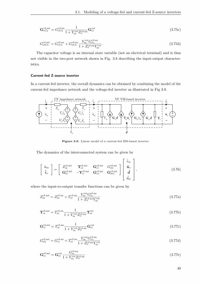
3.1. Modeling of a voltage-fed and current-fed Z-source inverters
Gvf-zsicCz = Gvf-zn
oCz1
1 + Y vsiin Zvf-zn
o
Gvsici (3.75c)
Gvf-zsistCz = Gvf-zn
cCz +Gvf-znoCz
Y vsiin Gvf-zn
co
1 + Zvf-zno Y vsi
in
. (3.75d)
The capacitor voltage is an internal state variable (not an electrical terminal) and is thus
not visible in the two-port network shown in Fig. 3.8 describing the input-output character-
istics.
Current-fed Z-source inverter
In a current-fed inverter, the overall dynamics can be obtained by combining the model of the
current-fed impedance network and the voltage-fed inverter as illustrated in Fig 3.9.
inY
ciˆG d
oi oˆT u
d
io dcuG
coˆG d
oY
ou
oi
dcu
dci
oZ
co stˆG d
io inˆG i
VF VSI-based inverterini
inu
ci stˆG d
oi dcˆT i
inZ
std
CF impedance network
Figure 3.9. Linear model of a current-fed ZSI-based inverter.
The dynamics of the interconnected system can be given by
[
uin
io
]
=
[
Zcf-zsiin Tcf-zsi
oi Gcf-zsici Gcf-zsi
sti
Gcf-zsiio −Ycf-zsi
o Gcf-zsico Gcf-zsi
sto
]
iin
uo
d
dst
, (3.76)
where the input-to-output transfer functions can be given by
Zcf-zsiin = Zcf-zn
in + T cf-znoi
Y vsiin Gcf-zn
io
1 + Zcf-zno Y vsi
in
(3.77a)
Tcf-zsioi = T cf-zn
oi1
1 + Y vsiin Zcf-zn
o
Tvsioi (3.77b)
Gcf-zsici = T cf-zn
oi1
1 + Y vsiin Zcf-zn
o
Gvsici (3.77c)
Gcf-zsisti = Gcf-zn
ci + T cf-znoi
Y vsiin Gcf-zn
co
1 + Zcf-zno Y vsi
in
(3.77d)
Gcf-zsiio = Gvsi
ioGcf-zn
io
1 + Y vsiin Zcf-zn
o
(3.77e)
49
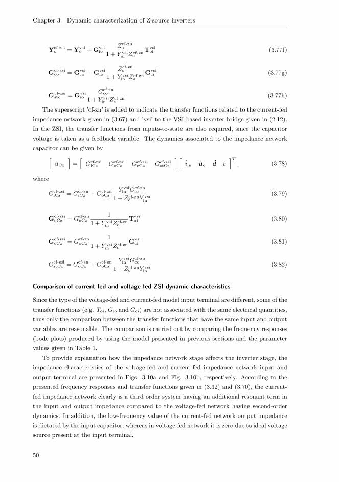
Chapter 3. Dynamic characterization of Z-source inverters
Ycf-zsio = Yvsi
o +Gvsiio
Zcf-zno
1 + Y vsiin Zcf-zn
o
Tvsioi (3.77f)
Gcf-zsico = Gvsi
co −Gvsiio
Zcf-zno
1 + Y vsiin Zcf-zn
o
Gvsici (3.77g)
Gvf-zsisto = Gvsi
ioGcf-zn
co
1 + Y vsiin Zcf-zn
o
(3.77h)
The superscript ’cf-zn’ is added to indicate the transfer functions related to the current-fed
impedance network given in (3.67) and ’vsi’ to the VSI-based inverter bridge given in (2.12).
In the ZSI, the transfer functions from inputs-to-state are also required, since the capacitor
voltage is taken as a feedback variable. The dynamics associated to the impedance network
capacitor can be given by
[
uCz
]
=[
Gcf-zsiiCz Gcf-zsi
oCz Gcf-zsicCz Gcf-zsi
stCz
] [
iin uo d c]T
, (3.78)
where
Gcf-zsiiCz = Gcf-zn
iCz +Gcf-znoCz
Y vsiin Gcf-zn
io
1 + Zcf-zno Y vsi
in
(3.79)
Gcf-zsioCz = Gcf-zn
oCz1
1 + Y vsiin Zcf-zn
o
Tvsioi (3.80)
Gcf-zsicCz = Gcf-zn
oCz1
1 + Y vsiin Zcf-zn
o
Gvsici (3.81)
Gcf-zsistCz = Gcf-zn
cCz +Gcf-znoCz
Y vsiin Gcf-zn
co
1 + Zcf-zno Y vsi
in
(3.82)
Comparison of current-fed and voltage-fed ZSI dynamic characteristics
Since the type of the voltage-fed and current-fed model input terminal are different, some of the
transfer functions (e.g. Toi, Gio and Gci) are not associated with the same electrical quantities,
thus only the comparison between the transfer functions that have the same input and output
variables are reasonable. The comparison is carried out by comparing the frequency responses
(bode plots) produced by using the model presented in previous sections and the parameter
values given in Table 1.
To provide explanation how the impedance network stage affects the inverter stage, the
impedance characteristics of the voltage-fed and current-fed impedance network input and
output terminal are presented in Figs. 3.10a and Fig. 3.10b, respectively. According to the
presented frequency responses and transfer functions given in (3.32) and (3.70), the current-
fed impedance network clearly is a third order system having an additional resonant term in
the input and output impedance compared to the voltage-fed network having second-order
dynamics. In addition, the low-frequency value of the current-fed network output impedance
is dictated by the input capacitor, whereas in voltage-fed network it is zero due to ideal voltage
source present at the input terminal.
50
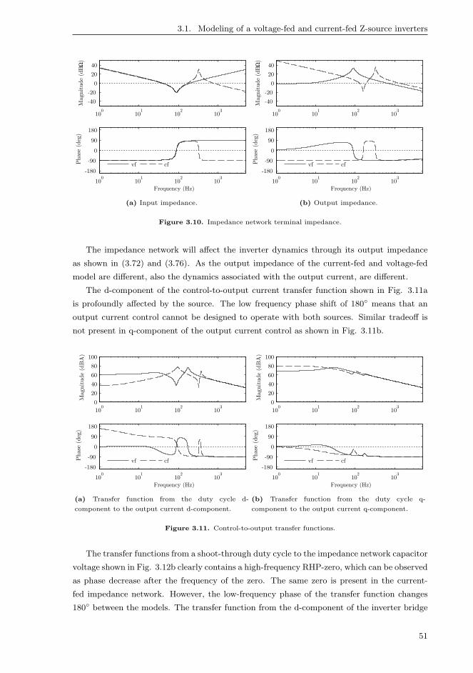
3.1. Modeling of a voltage-fed and current-fed Z-source inverters
100
101
102
103
-40
-20
0
20
40
Mag
nit
ude
(dB
Ω)
100
101
102
103
-180
-90
0
90
180
Phas
e (d
eg)
Frequency (Hz)
vf cf
(a) Input impedance.
100
101
102
103
-40
-20
0
20
40
Mag
nit
ude
(dB
Ω)
100
101
102
103
-180
-90
0
90
180
Phas
e (d
eg)
Frequency (Hz)
vf cf
(b) Output impedance.
Figure 3.10. Impedance network terminal impedance.
The impedance network will affect the inverter dynamics through its output impedance
as shown in (3.72) and (3.76). As the output impedance of the current-fed and voltage-fed
model are different, also the dynamics associated with the output current, are different.
The d-component of the control-to-output current transfer function shown in Fig. 3.11a
is profoundly affected by the source. The low frequency phase shift of 180 means that an
output current control cannot be designed to operate with both sources. Similar tradeoff is
not present in q-component of the output current control as shown in Fig. 3.11b.
100
101
102
103
0
20
40
60
80
100
Mag
nit
ude
(dB
A)
100
101
102
103
-180
-90
0
90
180
Phas
e (d
eg)
Frequency (Hz)
vf cf
(a) Transfer function from the duty cycle d-
component to the output current d-component.
100
101
102
103
0
20
40
60
80
100
Mag
nit
ude
(dB
A)
100
101
102
103
-180
-90
0
90
180
Phas
e (d
eg)
Frequency (Hz)
vf cf
(b) Transfer function from the duty cycle q-
component to the output current q-component.
Figure 3.11. Control-to-output transfer functions.
The transfer functions from a shoot-through duty cycle to the impedance network capacitor
voltage shown in Fig. 3.12b clearly contains a high-frequency RHP-zero, which can be observed
as phase decrease after the frequency of the zero. The same zero is present in the current-
fed impedance network. However, the low-frequency phase of the transfer function changes
180 between the models. The transfer function from the d-component of the inverter bridge
51
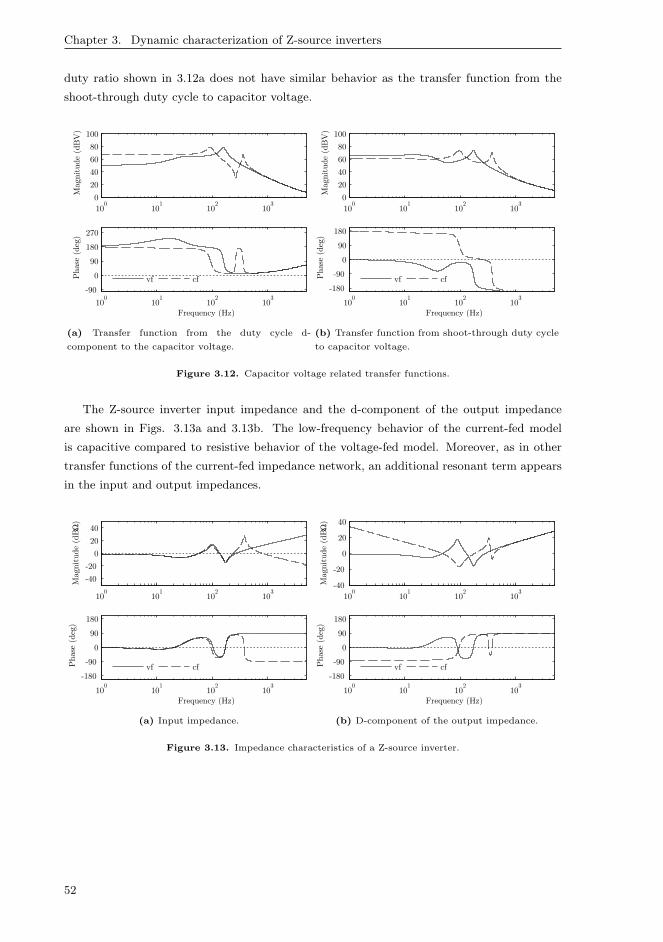
Chapter 3. Dynamic characterization of Z-source inverters
duty ratio shown in 3.12a does not have similar behavior as the transfer function from the
shoot-through duty cycle to capacitor voltage.
100
101
102
103
0
20
40
60
80
100
Mag
nit
ude
(dB
V)
100
101
102
103
-90
0
90
180
270
Phas
e (d
eg)
Frequency (Hz)
vf cf
(a) Transfer function from the duty cycle d-
component to the capacitor voltage.
100
101
102
103
0
20
40
60
80
100
Mag
nit
ude
(dB
V)
100
101
102
103
-180
-90
0
90
180
Phas
e (d
eg)
Frequency (Hz)
vf cf
(b) Transfer function from shoot-through duty cycle
to capacitor voltage.
Figure 3.12. Capacitor voltage related transfer functions.
The Z-source inverter input impedance and the d-component of the output impedance
are shown in Figs. 3.13a and 3.13b. The low-frequency behavior of the current-fed model
is capacitive compared to resistive behavior of the voltage-fed model. Moreover, as in other
transfer functions of the current-fed impedance network, an additional resonant term appears
in the input and output impedances.
100
101
102
103
-40
-20
0
20
40
Mag
nit
ude
(dB
Ω)
100
101
102
103
-180
-90
0
90
180
Phas
e (d
eg)
Frequency (Hz)
vf cf
(a) Input impedance.
100
101
102
103
-40
-20
0
20
40
Mag
nit
ude
(dB
Ω)
100
101
102
103
-180
-90
0
90
180
Phas
e (d
eg)
Frequency (Hz)
vf cf
(b) D-component of the output impedance.
Figure 3.13. Impedance characteristics of a Z-source inverter.
52

3.2. Modeling of a photovoltaic Z-source inverter
Table 3.1. Z-source inverter parameters used in comparison.
Uin Iin Pin Udc Uo-rms
400 V 25 A 10 kW 700 V 230 V (at 50 Hz)
C1, C2 L1, L2 Cin L UD
500 µF 1 mH 250 µF 800 mH 0.7 V
rC1, rC2 rL1, rL2 rCin rL + rsw rD
10 mΩ 50 mΩ 10 mΩ 100 mΩ 20 mΩ
3.2 Modeling of a photovoltaic Z-source inverter
The model of a photovoltaic Z-source inverter shown in Fig. 3.14, is derived by first computing
the effect of the photovoltaic generator on the dynamics of the impedance network. Then it
is combined with the model of the VSI-based inverter.
Lr L
o-(a,b,c)i
o-(a,b,c)u
L-(a,b,c)u
dcu
a
b
cn
L-(a,b,c)i
N
Ppi
cpS
bpS
apS
cnS
bnS
anS
pvi
Cinr
inC
Cinu
pvu
C2u
L1u
L1i
L1r
1L
C2r
2C
1C
C1r
L2u
L2i
2L L2
r
C1u
Cini
C1iC2
i
Figure 3.14. Three-phase photovoltaic inverter based on conventional ZSI-topology.
Effect of the photovoltaic generator on dynamics of the impedance network
The photovoltaic generator is a highly non-linear source having properties of a voltage source
and a current source. To design robust controllers for the interfacing inverter, a method to
include the effect of the dual nature of the source is required. The most straightforward
method to include the effect is to use the source-affected model of the current-fed impedance
network.
The source-affected small-signal characteristics of the current-fed impedance network can
be given as
[
upv
io
]
=
[
ZSin T S
oi GSci
GSio −ZS
o GSco
]
iph
udc
d
, (3.83)
where the source-affected transfer functions denoted by superscript ’S’ are
ZSin =
Zin
1 + YpvZin(3.84a)
53
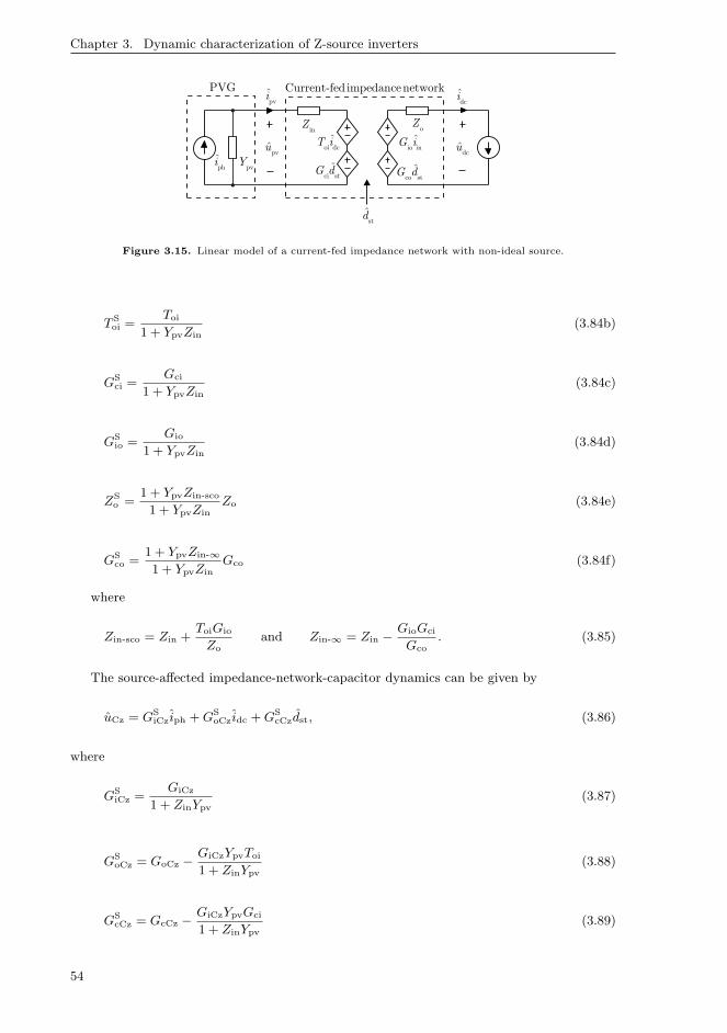
Chapter 3. Dynamic characterization of Z-source inverters
dcu
dci
oZ
co stˆG d
io inˆG i
ci stˆG d
oi dcˆT i
inZ
std
phi
pvY
PVG
pvu
pvi
Current-fed impedancenetwork
Figure 3.15. Linear model of a current-fed impedance network with non-ideal source.
T Soi =
Toi
1 + YpvZin(3.84b)
GSci =
Gci
1 + YpvZin(3.84c)
GSio =
Gio
1 + YpvZin(3.84d)
ZSo =
1 + YpvZin-sco
1 + YpvZinZo (3.84e)
GSco =
1 + YpvZin-∞
1 + YpvZinGco (3.84f)
where
Zin-sco = Zin +ToiGio
Zoand Zin-∞ = Zin −
GioGci
Gco. (3.85)
The source-affected impedance-network-capacitor dynamics can be given by
uCz = GSiCz iph +GS
oCz idc +GScCzdst, (3.86)
where
GSiCz =
GiCz
1 + ZinYpv(3.87)
GSoCz = GoCz −
GiCzYpvToi
1 + ZinYpv(3.88)
GScCz = GcCz −
GiCzYpvGci
1 + ZinYpv(3.89)
54
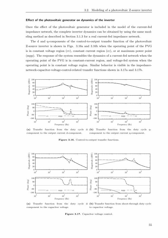
3.2. Modeling of a photovoltaic Z-source inverter
Effect of the photovoltaic generator on dynamics of the inverter
Once the effect of the photovoltaic generator is included in the model of the current-fed
impedance network, the complete inverter dynamics can be obtained by using the same mod-
eling method as described in Section 3.1.3 for a real current-fed impedance network.
The d and q-components of the control-to-output transfer function of the photovoltaic
Z-source inverter is shown in Figs. 3.16a and 3.16b when the operating point of the PVG
is in constant voltage region (cv), constant current region (cc), or at maximum power point
(mpp). The response of the system resembles the dynamics of a current-fed network when the
operating point of the PVG is in constant-current region, and voltage-fed system when the
operating point is in constant voltage region. Similar behavior is visible in the impedance-
network-capacitor-voltage-control-related transfer functions shown in 3.17a and 3.17b.
100
101
102
103
0
20
40
60
80
100
Mag
nit
ude
(dB
A)
100
101
102
103
-180
-90
0
90
180
Phas
e (d
eg)
Frequency (Hz)
cv mpp cc
(a) Transfer function from the duty cycle d-
component to the output current d-component.
100
101
102
103
0
20
40
60
80
100
Mag
nit
ude
(dB
A)
100
101
102
103
-180
-90
0
90
180
Phas
e (d
eg)
Frequency (Hz)
cv mpp cc
(b) Transfer function from the duty cycle q-
component to the output current q-component.
Figure 3.16. Control-to-output transfer functions.
100
101
102
103
0
20
40
60
80
100
Mag
nit
ude
(dB
V)
100
101
102
103
-180
-90
0
90
180
Phas
e (d
eg)
Frequency (Hz)
cv mpp cc
(a) Transfer function from the duty cycle d-
component to the capacitor voltage.
100
101
102
103
0
20
40
60
80
100
Mag
nit
ude
(dB
V)
100
101
102
103
-180
-90
0
90
180
Phas
e (d
eg)
Frequency (Hz)
cv mpp cc
(b) Transfer function from shoot-through duty cycle
to capacitor voltage.
Figure 3.17. Capacitor voltage control.
55
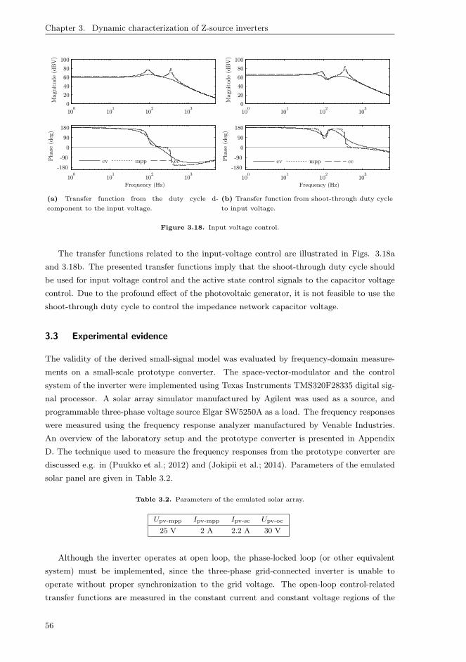
Chapter 3. Dynamic characterization of Z-source inverters
100
101
102
103
0
20
40
60
80
100M
agnit
ude
(dB
V)
100
101
102
103
-180
-90
0
90
180
Phas
e (d
eg)
Frequency (Hz)
cv mpp cc
(a) Transfer function from the duty cycle d-
component to the input voltage.
100
101
102
103
0
20
40
60
80
100
Mag
nit
ude
(dB
V)
100
101
102
103
-180
-90
0
90
180
Phas
e (d
eg)
Frequency (Hz)
cv mpp cc
(b) Transfer function from shoot-through duty cycle
to input voltage.
Figure 3.18. Input voltage control.
The transfer functions related to the input-voltage control are illustrated in Figs. 3.18a
and 3.18b. The presented transfer functions imply that the shoot-through duty cycle should
be used for input voltage control and the active state control signals to the capacitor voltage
control. Due to the profound effect of the photovoltaic generator, it is not feasible to use the
shoot-through duty cycle to control the impedance network capacitor voltage.
3.3 Experimental evidence
The validity of the derived small-signal model was evaluated by frequency-domain measure-
ments on a small-scale prototype converter. The space-vector-modulator and the control
system of the inverter were implemented using Texas Instruments TMS320F28335 digital sig-
nal processor. A solar array simulator manufactured by Agilent was used as a source, and
programmable three-phase voltage source Elgar SW5250A as a load. The frequency responses
were measured using the frequency response analyzer manufactured by Venable Industries.
An overview of the laboratory setup and the prototype converter is presented in Appendix
D. The technique used to measure the frequency responses from the prototype converter are
discussed e.g. in (Puukko et al.; 2012) and (Jokipii et al.; 2014). Parameters of the emulated
solar panel are given in Table 3.2.
Table 3.2. Parameters of the emulated solar array.
Upv-mpp Ipv-mpp Ipv-sc Upv-oc
25 V 2 A 2.2 A 30 V
Although the inverter operates at open loop, the phase-locked loop (or other equivalent
system) must be implemented, since the three-phase grid-connected inverter is unable to
operate without proper synchronization to the grid voltage. The open-loop control-related
transfer functions are measured in the constant current and constant voltage regions of the
56
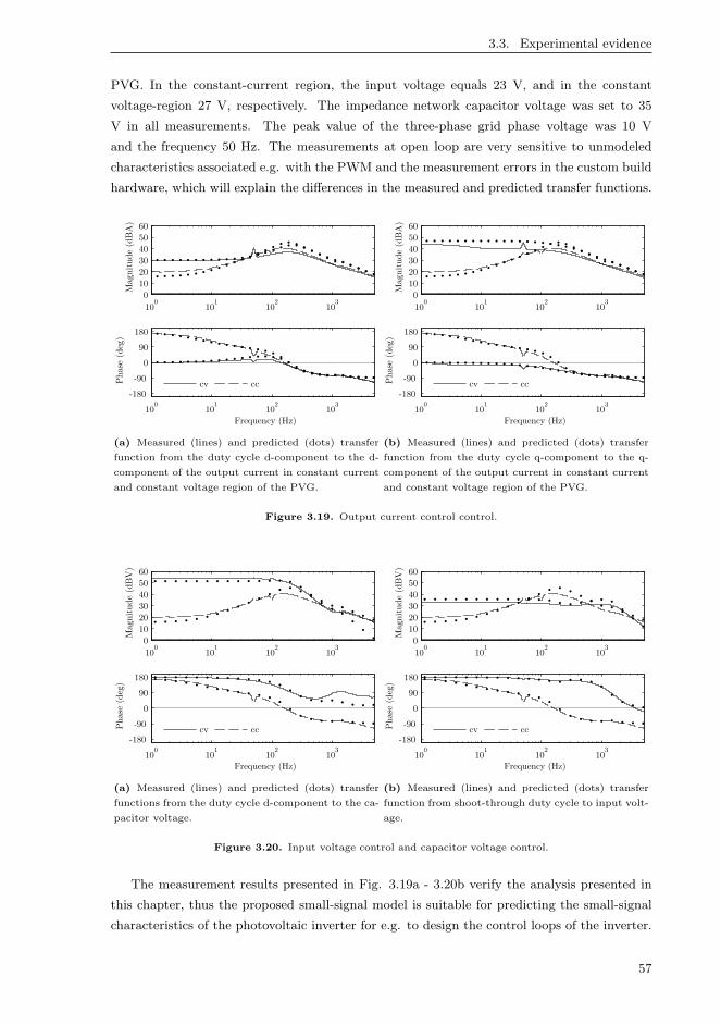
3.3. Experimental evidence
PVG. In the constant-current region, the input voltage equals 23 V, and in the constant
voltage-region 27 V, respectively. The impedance network capacitor voltage was set to 35
V in all measurements. The peak value of the three-phase grid phase voltage was 10 V
and the frequency 50 Hz. The measurements at open loop are very sensitive to unmodeled
characteristics associated e.g. with the PWM and the measurement errors in the custom build
hardware, which will explain the differences in the measured and predicted transfer functions.
100
101
102
103
0
10
20
30
40
50
60
Mag
nit
ude
(dB
A)
100
101
102
103
-180
-90
0
90
180
Phas
e (d
eg)
Frequency (Hz)
cv cc
(a) Measured (lines) and predicted (dots) transfer
function from the duty cycle d-component to the d-
component of the output current in constant current
and constant voltage region of the PVG.
100
101
102
103
0
10
20
30
40
50
60
Mag
nit
ude
(dB
A)
100
101
102
103
-180
-90
0
90
180
Phas
e (d
eg)
Frequency (Hz)
cv cc
(b) Measured (lines) and predicted (dots) transfer
function from the duty cycle q-component to the q-
component of the output current in constant current
and constant voltage region of the PVG.
Figure 3.19. Output current control control.
100
101
102
103
0
10
20
30
40
50
60
Mag
nit
ude
(dB
V)
100
101
102
103
-180
-90
0
90
180
Phas
e (d
eg)
Frequency (Hz)
cv cc
(a) Measured (lines) and predicted (dots) transfer
functions from the duty cycle d-component to the ca-
pacitor voltage.
100
101
102
103
0
10
20
30
40
50
60
Mag
nit
ude
(dB
V)
100
101
102
103
-180
-90
0
90
180
Phas
e (d
eg)
Frequency (Hz)
cv cc
(b) Measured (lines) and predicted (dots) transfer
function from shoot-through duty cycle to input volt-
age.
Figure 3.20. Input voltage control and capacitor voltage control.
The measurement results presented in Fig. 3.19a - 3.20b verify the analysis presented in
this chapter, thus the proposed small-signal model is suitable for predicting the small-signal
characteristics of the photovoltaic inverter for e.g. to design the control loops of the inverter.
57

Chapter 3. Dynamic characterization of Z-source inverters
3.4 Conclusions
In this chapter, a model for a voltage-fed and a current-fed three-phase grid-connected Z-source
inverters was derived. Moreover, using the proposed models it was concluded that the voltage-
fed model fails to predict the characteristics of the Z-source inverter when it is supplied from a
current source. Thus to represent the dynamics of the Z-source inverter correctly, the system
input variables must be selected based on the real application environment. The correct model
for a photovoltaic grid-connected Z-source inverter can be constructed by combining the model
of a source-affected current-fed impedance network and the model of the VSI-based inverter.
The transfer functions presented in this chapter can be used to study the effect of inverter
parameters to the shape of the transfer functions and location of the resonances associated to
the converter dynamics and design the control loops of the inverter. The derived model also
imply that since the source impedance has profound effect of the shoot-through duty cycle to
the impedance network capacitor voltage, the shoot-through duty cycle should not be used for
capacitor voltage control in photovoltaic applications. Instead, the shoot-through duty cycle
should be used for the input-voltage control.
58
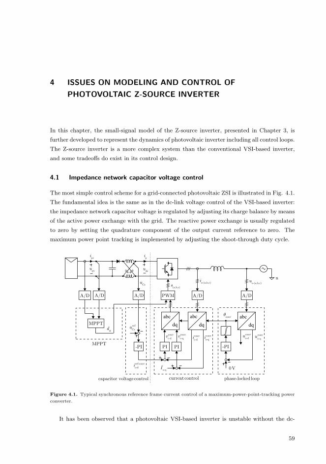
4 ISSUES ON MODELING AND CONTROL OF
PHOTOVOLTAIC Z-SOURCE INVERTER
In this chapter, the small-signal model of the Z-source inverter, presented in Chapter 3, is
further developed to represent the dynamics of photovoltaic inverter including all control loops.
The Z-source inverter is a more complex system than the conventional VSI-based inverter,
and some tradeoffs do exist in its control design.
4.1 Impedance network capacitor voltage control
The most simple control scheme for a grid-connected photovoltaic ZSI is illustrated in Fig. 4.1.
The fundamental idea is the same as in the dc-link voltage control of the VSI-based inverter:
the impedance network capacitor voltage is regulated by adjusting its charge balance by means
of the active power exchange with the grid. The reactive power exchange is usually regulated
to zero by setting the quadrature component of the output current reference to zero. The
maximum power point tracking is implemented by adjusting the shoot-through duty cycle.
-PI
0V
ò
convq
conv
o-du conv
o-qu
dq
abc
conv
o-di
conv
o-qi
conv
c-dv
conv
c-qv
PI PI
o-qI
(a,b,c)s
///
o-(a,b,c)i
///
A/D
///
/// o-(a,b,c)
u
///
A/D
/// n
dq
abc
dq
abc
///
phase-locked loopcurrentcontrol
A/D
std
capacitor voltage control
pvu
pvi
pi
dcu
A/D
MPPT
ref-conv
o-di
A/D
-PI
ref
Czu
MPPT
Czu
PWM
Figure 4.1. Typical synchronous reference frame current control of a maximum-power-point-tracking power
converter.
It has been observed that a photovoltaic VSI-based inverter is unstable without the dc-
59

Chapter 4. Issues on modeling and control of photovoltaic Z-source inverter
link-voltage control when the operating point of the PVG is in the constant-current region.
The instability is caused by the low-frequency RHP-zero associated to the d-component of the
output current control, which becomes a low-frequency rhp-pole when high-bandwidth current
control is activated (Puukko and Suntio; 2012). As the high-bandwidth current control is
must in a grid-connected inverter, the dc-link-voltage-control loop having the loop crossover
frequency higher than the frequency of the pole is required to stabilize the system. Since the
circuit structures of photovoltaic VSI and ZSI-based inverters are similar, the same behavior
is present also in Z-source inverter. However, since the transfer functions of the system are of
fifth order, the system analysis cannot be carried out by using the full-order transfer functions,
which is possible in the VSI-based inverter.
The instability can be explained by studying the control block diagram showing the in-
terconnection of the source-affected current-fed impedance network and the output-current-
controlled VSI-based inverter illustrated in Fig. 4.2. An internal feedback loop including
the output impedance ZznSo of the source subsystem (the impedance network) and input ad-
mittance Y vsi-outin of load subsystem (current-controlled VSI-based inverter) is created. As
a consequence, every transfer function representing the interconnected system includes the
internal feedback loop, e.g. the transfer function from the output-current reference to the
dc-link current in the interconnected system can be given by
idc =1
1 + Zzn-So Y vsi-out
in
Gvsi-outci i
refo . (4.1)
According to Middlebrook, the ratio between the source and load impedance as in (4.2) is
known as the minor loop gain of a voltage-fed interface. It has been shown that the stability
of the interconnected system can be analyzed by studying the minor-loop gain similarly as
the loop-gain of a negative feedback control system. As the source and load are stable as
standalone systems, the Nyquist criterion can be used to determine the stability. In the
simplified version of analysis, the denominator of the loop gain becomes infinite if the source
and load impedance are equal and have the phase difference of 180.
L = Zzn-So Y vsi-out
in =Zzn-S
o
Zvsi-outin
. (4.2)
Due to the high-bandwidth output-current control, the input terminal of a output current-
controlled voltage-fed VSI-based inverter resembles constant power sink inside the current-
control bandwidth, i.e., the low-frequency value of the input admittance can be given by:
Y vsi-outin-lf = −
IdcUdc
(4.3)
The instability thus can take place if the source impedance Zzn-So is higher than Udc/Idc.
When the inverter is fed from a voltage-type source, the source impedance is low and the
condition Zo < Udc/Idc is met regardless of the small variations in the output impedance of
the source. However, if the source impedance is high at certain frequencies, the instability may
take place. According to the model presented in Chapters 3 and 4, in the Z-source inverter,
the impedance seen by the inverter bridge is the low-frequency output impedance of the PVG
60
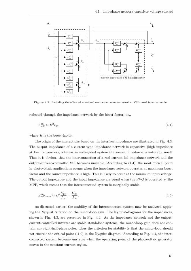
4.1. Impedance network capacitor voltage control
out
inY
out
oiT
out
ioG
out
o-Y
out
coG
out
ciG
ref
oi
ou
oi
dcu dc
i
current-controlledVSI-based inverter
S
inZ
pvu
iphˆ
S
oiT
std
dcu
S
ciG
S
oZ-
S
coG
S
ioG
Czu
S
oCzG
S
cCzG
S
iCzG
pvu
Figure 4.2. Including the effect of non-ideal source on current-controlled VSI-based inverter model.
reflected through the impedance network by the boost-factor, i.e.,
Zzno-lf ≈ B2rpv, (4.4)
where B is the boost-factor.
The origin of the interactions based on the interface impedance are illustrated in Fig. 4.3.
The output impedance of a current-type impedance network is capacitive (high impedance
at low frequencies), whereas in voltage-fed system the source impedance is naturally small.
Thus it is obvious that the interconnection of a real current-fed impedance network and the
output-current-controlled VSI becomes unstable. According to (4.4), the most critical point
in photovoltaic applications occurs when the impedance network operates at maximum boost
factor and the source impedance is high. This is likely to occur at the minimum input voltage.
The output impedance and the input impedance are equal when the PVG is operated at the
MPP, which means that the interconnected system is marginally stable.
Zzno-lf-mpp ≈ B2Upv
Ipv=
Udc
Idc, (4.5)
As discussed earlier, the stability of the interconnected system may be analyzed apply-
ing the Nyquist criterion on the minor-loop gain. The Nyquist-diagrams for the impedances,
shown in Fig. 4.3, are presented in Fig. 4.4. As the impedance network and the output-
current-controlled inverter are stable standalone systems, the minor-loop gain does not con-
tain any right-half-plane poles. Thus the criterion for stability is that the minor-loop should
not encircle the critical point (-1,0) in the Nyquist diagram. According to Fig. 4.4, the inter-
connected system becomes unstable when the operating point of the photovoltaic generator
moves to the constant-current region.
61
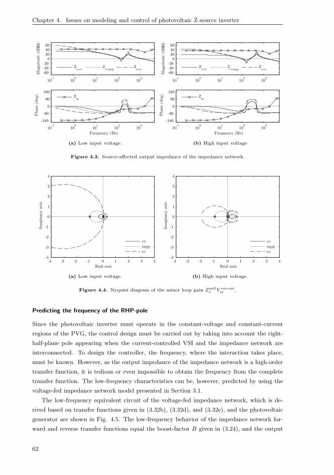
Chapter 4. Issues on modeling and control of photovoltaic Z-source inverter
10-1
100
101
102
103
-60-40-20
0204060
Mag
nit
ude
(dB
Ω)
Zo-cv
Zo-mpp
Zo-cc
10-1
100
101
102
103
-180
-90
0
90
180
Phas
e (d
eg)
Frequency (Hz)
Zin
(a) Low input voltage.
10-1
100
101
102
103
-60-40-20
0204060
Mag
nit
ude
(dB
Ω)
Zo-cv
Zo-mpp
Zo-cc
10-1
100
101
102
103
-180
-90
0
90
180
Phas
e (d
eg)
Frequency (Hz)
Zin
(b) High input voltage
Figure 4.3. Source-affected output impedance of the impedance network.
-4 -3 -2 -1 0 1 2 3 4-4
-3
-2
-1
0
1
2
3
4
Imagin
ary
axis
Real axis
cv
mpp
cc
(a) Low input voltage.
-4 -3 -2 -1 0 1 2 3 4-4
-3
-2
-1
0
1
2
3
4
Imagin
ary
axis
Real axis
cv
mpp
cc
(b) High input voltage.
Figure 4.4. Nyquist diagram of the minor loop gain ZznSo Y
vsi-outin .
Predicting the frequency of the RHP-pole
Since the photovoltaic inverter must operate in the constant-voltage and constant-current
regions of the PVG, the control design must be carried out by taking into account the right-
half-plane pole appearing when the current-controlled VSI and the impedance network are
interconnected. To design the controller, the frequency, where the interaction takes place,
must be known. However, as the output impedance of the impedance network is a high-order
transfer function, it is tedious or even impossible to obtain the frequency from the complete
transfer function. The low-frequency characteristics can be, however, predicted by using the
voltage-fed impedance network model presented in Section 3.1.
The low-frequency equivalent circuit of the voltage-fed impedance network, which is de-
rived based on transfer functions given in (3.32b), (3.32d), and (3.32e), and the photovoltaic
generator are shown in Fig. 4.5. The low-frequency behavior of the impedance network for-
ward and reverse transfer functions equal the boost-factor B given in (3.24), and the output
62
4.1. Impedance network capacitor voltage control
impedance of the network is negligible. The input admittance of the low-frequency model
equals the input admittance of the voltage-fed model given in (3.32a).
dcu
dci
in-lfY
1 : B
phi
pvY
VF-impedancenetwork
CinY
Figure 4.5. Linear circuit used for output impedance approximation.
When a parallel connection of an input capacitor and photovoltaic generator are taken
into account, the low-frequency behavior of the impedance network, according to the Fig. 4.5,
can be given as
Zzno-lf ≈ B2Y −1
eq , (4.6)
where
Yeq = Ypv + Yin-lf + YCin. (4.7)
Inserting the low frequency input admittance of the voltage-fed impedance network (3.32a),
admittance of the input capacitor (sCin), and the admittance of the PVG (1/rpv) into (4.6)
yields
Zzno-lf ≈
B2rpvsrpv (Cin + 2B2(1−Dst)2C1) + 1
. (4.8)
The output impedance of the source-affected current-fed impedance network computed
by using the full-order model given in Section 3.2 and the approximated output impedance
using (4.8) are shown in Fig. 4.6. According to the figure, the approximation predicts the
low-frequency characteristics correctly at the different operating points of the PVG.
Finally, when the approximation for the source and load impedance are known, the pole
frequency of the interconnected system can be found by solving the characteristic equation
1−B2rpv
srpv (Cin + 2B2(1−Dst)2C1) + 1·IdcUdc
= 0. (4.9)
The frequency of the pole can be solved from (4.9) yielding
ωp =1
Cin + 2U2
Cz
U2pv
C1
(IpvUpv
−1
rpv
)
. (4.10)
The pole frequency is positive, i.e. it locates in the right-half of the complex plane, when
rpv > Upv/Ipv. Correspondingly, when rpv < Upv/Ipv, the pole frequency is negative and it
locates in the left-half of the complex plane. The maximum right-half-plane pole frequency
can be determined assuming infinite rpv, i.e., a real current-fed inverter. According to (4.10),
the maximum RHP frequency can be given as
ωp-rhp =1
U2pvCin + 2U2
CzC1Ppv. (4.11)
63
Chapter 4. Issues on modeling and control of photovoltaic Z-source inverter
10-1
100
101
102
103
-60-40-20
0204060
Mag
nit
ude
(dB
Ω)
10-1
100
101
102
103
-180
-90
0
90
180
Phas
e (d
eg)
Frequency (Hz)
original approximation
(a) Constant-voltage region.
10-1
100
101
102
103
-60-40-20
0204060
Mag
nit
ude
(dB
Ω)
10-1
100
101
102
103
-180
-90
0
90
180
Phas
e (d
eg)
Frequency (Hz)
original approximation
(b) Constant-current region.
Figure 4.6
At low input voltages, the frequency given by (4.11) is dominated by the second term in the
denominator (i.e. U2pv << 2U2
Cz). Thus maximum frequency of the pole can be approximated
as
ωp-rhp < ωp-rhp-max ≈1
2U2CzC1
Ppv. (4.12)
When the converter operates in buck-mode, the input voltage and the impedance network
capacitor voltages are equal. The most critical condition occurs when the voltage gets its
minimum value and the current its maximum value, i.e.,
ωp-rhp < ωp-rhp-max ≈1
U2pv(Cin + 2C1)
Ppv =Ipv
Upv(Cin + 2C1)(4.13)
Impedance network capacitor voltage control
The impedance-network-capacitor-voltage control is required to maintain the stability of the
inverter, since it is required to stabilize the right-half-plane plane pole caused by the current-
type source and grid-current control. The photovoltaic inverter equipped with only output-
current control becomes unstable when the operating point moves into the constant current
region of the PVG. Fortunately, the feedback from e.g. the capacitor voltage will stabilize the
system if the control bandwidth (loop crossover frequency) is higher than the frequency of the
unstable pole (Skogestad and Postlethwaite; 2005).
According to Fig. 4.2, the transfer function from output current reference to the equivalent
dc-link current can be given by
idc =1
1 + ZznSo Y vsi-out
in
Gvsi-outci i
refo . (4.14)
As only the d-component of the current reference is used in control, (4.14) may be rewritten
by
idc =1
1 + ZznSo Y vsi-out
in
Gvsi-outci-d irefo-d (4.15)
64

4.1. Impedance network capacitor voltage control
Finally, the transfer function from the direct component of the output-current reference
to the capacitor-voltage according to Fig. 4.2 can be given by
GioCz = GznSoCz
1
1 + Y vsi-outin ZznS
o
Gvsi-outci-d irefo-d (4.16)
An example Nyquist diagrams of the loop-gains of a stable and unstable capacitor-voltage-
control loop is shown in Fig. 4.7. When the operating point of the PVG is in CC region, the
output current controlled system has one unstable pole. The nyquist diagram of the loop gain
should thus encircle the critical point once to obtain stable closed-loop system. If the control
loop gain is decreased (or the size of the capacitor decreased), the loop gain does not encircle
the point and the closed loop system remains unstable.
-4 -3.5 -3 -2.5 -2 -1.5 -1 -0.5 0 0.5 1 1.5 2-2
-1.5
-1
-0.5
0
0.5
1
1.5
2
Imagin
ary
axis
Real axis
K=0.05
K=0.01
Figure 4.7. Nyquist diagram of the loop gain GCzc GioCz.
Finally, the closed-loop transfer function including the effect of the capacitor-voltage con-
trol is found by substituting the current reference by the output of the impedance network-
capacitor-voltage controller similarly as in VSI-based inverter presented in Chapter 2, or
alternatively from the control-block diagram shown in Fig. 4.8. The resulting closed-loop
transfer functions of the Z-source inverter can be given by
[
upv
io
]
=
[
Zcin Tc
oi Gcri Gc
sti
Gcio −Yc
o Gcro Gc
sto
]
iph
uo
urefCz
dst
, (4.17)
where
Zcin = ZoutS
in −GoutSri-d
GuCzc
1 +GuCzc GoutS
rCz-d
GoutSiCz (4.18)
Tcoi = ToutS
oi −GoutSri-d
GuCzc
1 +GuCzc GoutS
rCz-d
GoutSoCz (4.19)
Gcri =
GoutSri-d Gudc
c
1 +GoutSrCz-dG
uinc
(4.20)
65
Chapter 4. Issues on modeling and control of photovoltaic Z-source inverter
Gcsti = GoutS
sti −GoutSri-d
GuCzc
1 +GuCzc GoutS
rCz-d
GoutSstCz (4.21)
Gcio = GoutS
io −GoutSro-d G
rCzc
1
1 +GoutSrCz-dG
udcc
GoutSiCz (4.22)
Yco = YoutS
o +GoutSro-d G
uCzc
1
1 +GoutSrCz GuCz
c
GoutSoCz (4.23)
Gcro = GoutS
roGudc
c
1 +GoutSrCz-dG
uinc
(4.24)
Gcsto = GoutS
sto −GoutSro
GuCzc
1 +GuCzc GoutS
rCz-d
GoutSstCz . (4.25)
ou
oi
pvu
iphˆ
std
Czu
uCz
seG
uCz
cG
ref
Czuref
o-di
outS
ro-dG
outS
inZ
outS
oiT
outS
stiG
outS
oY
outS
stoG
outS
ioG
outS
oCzG
outS
stCzG
outS
iCzG outS
rCz-dG
outS
ri-dG
Figure 4.8. Including the effect of non-ideal source on current-controlled Z-source inverter model. The
mode inside the dashed are equals the model given in Fig. 4.2.
4.2 Determining the value of minimum impedance network capacitance
As discussed in the previous section, the impedance-network-capacitor-voltage control is re-
quired to obtain stable closed-loop control system at all operating points of the photovoltaic
generator. The crossover frequency of the capacitor voltage-loop must be higher than the pole
frequency. According to (Skogestad and Postlethwaite; 2005), the frequency should be twice
the unstable pole. In an ideal converter and ideal grid, this can be easily guaranteed. How-
ever, in practice it is not feasible to use too high control bandwidth due to the ripple at the
frequency of twice the grid frequency caused e.g. by the unbalance in the grid voltages. The
control system should be designed to attenuate the ripple generated by the power oscillation,
otherwise the grid current will be distorted. As a consequence, the capacitor-voltage-control-
loop crossover has to be limited to few tens of hertz. As the frequency of the pole is dictated
by the impedance network capacitor voltage and the power of the photovoltaic generator, the
66
4.3. Effect of control-mode on control system performance
minimum size for the impedance network capacitor can be analyzed as has been previously
done for single and two-stage VSI in Messo et al. (2014).
According to the analysis presented in the previous section, the maximum pole frequency
in the Z-source inverter equals
ωp-max ≈1
2U2CzC1
Ppv (4.26)
When the cloud enhancement (Luoma et al.; 2012) (sudden increase in the power pro-
duced by the PVG may increase 1.5 times the nominal power) and the safety margin of
two (Skogestad and Postlethwaite; 2005) are considered, a tradeoff between loop crossover
frequency, impedance-network-capacitor voltage, and the minimum impedance network ca-
pacitance can be formulated as
2πfc > 2 · 1.5 · ωp ⇒ C1 >2 · 1.5
2U2Cz2πfc
Ppv-mpp, (4.27)
where fc is the crossover frequency of the impedance-network-capacitor-voltage-control-loop
gain. The required capacitance to guarantee stability is illustrated in Fig. 4.9. By using
a higher steady state capacitor voltage, a smaller capacitor could be used. However, as
a drawback the switching losses will increase. E.g. in 10 kW inverter, where the capacitor
voltage is set to 700 V, and the loop-crossover equals 10 Hz, the required capacitance according
to (4.27) equals 500 µF.
0 10 20 30 40 50 60 70 800
10
20
30
40
50
60
70
80
Loop crossover frequency (Hz)
Cap
acit
ance
/Pow
er (
F/k
W)
μ
UCz
= 590 V
UCz
= 680 V
stable region + safety margin
stable region
unstable region
Figure 4.9. Minimum impedance network capacitance requirement for Z-source inverter.
As the pole frequency given by (4.26) does not contain the input capacitance, the input
capacitor can be selected to based only on the ripple requirement induced by the PVG.
4.3 Effect of control-mode on control system performance
The impedance network of the Z-source inverter may operate in two modes: i) at open loop
as in Section 4.1, or ii) at closed loop as shown in Fig. 4.10, where a feedback loop is added
to regulate the input voltage of the converter. The addition of the input-voltage control, as
in case of two-stage VSI-based inverter, will improve the MPP tracking performance, and it
67
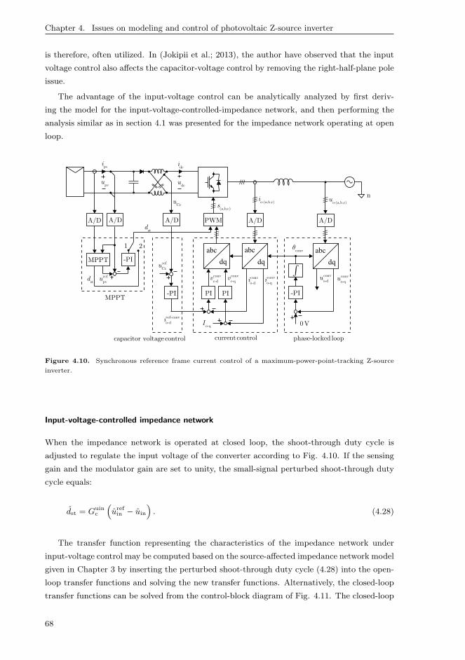
Chapter 4. Issues on modeling and control of photovoltaic Z-source inverter
is therefore, often utilized. In (Jokipii et al.; 2013), the author have observed that the input
voltage control also affects the capacitor-voltage control by removing the right-half-plane pole
issue.
The advantage of the input-voltage control can be analytically analyzed by first deriv-
ing the model for the input-voltage-controlled-impedance network, and then performing the
analysis similar as in section 4.1 was presented for the impedance network operating at open
loop.
-PI
0V
ò
convq
conv
o-du conv
o-qu
dq
abc
conv
o-di
conv
o-qi
conv
c-dv
conv
c-qv
PI PI
o-qI
(a,b,c)s
///
o-(a,b,c)i
///
A/D
///
/// o-(a,b,c)
u
///
A/D
/// n
dq
abc
dq
abc
///
phase-locked loopcurrentcontrol
A/D
ref
pvu
capacitor voltage control
pvu
pvi
dci
dcu
A/D
MPPT
ref-conv
o-di
A/D
-PI
ref
Czu
MPPT
-PI
Czu
PWM
std
std
21
Figure 4.10. Synchronous reference frame current control of a maximum-power-point-tracking Z-source
inverter.
Input-voltage-controlled impedance network
When the impedance network is operated at closed loop, the shoot-through duty cycle is
adjusted to regulate the input voltage of the converter according to Fig. 4.10. If the sensing
gain and the modulator gain are set to unity, the small-signal perturbed shoot-through duty
cycle equals:
dst = Guinc
(
urefin − uin
)
. (4.28)
The transfer function representing the characteristics of the impedance network under
input-voltage control may be computed based on the source-affected impedance network model
given in Chapter 3 by inserting the perturbed shoot-through duty cycle (4.28) into the open-
loop transfer functions and solving the new transfer functions. Alternatively, the closed-loop
transfer functions can be solved from the control-block diagram of Fig. 4.11. The closed-loop
68
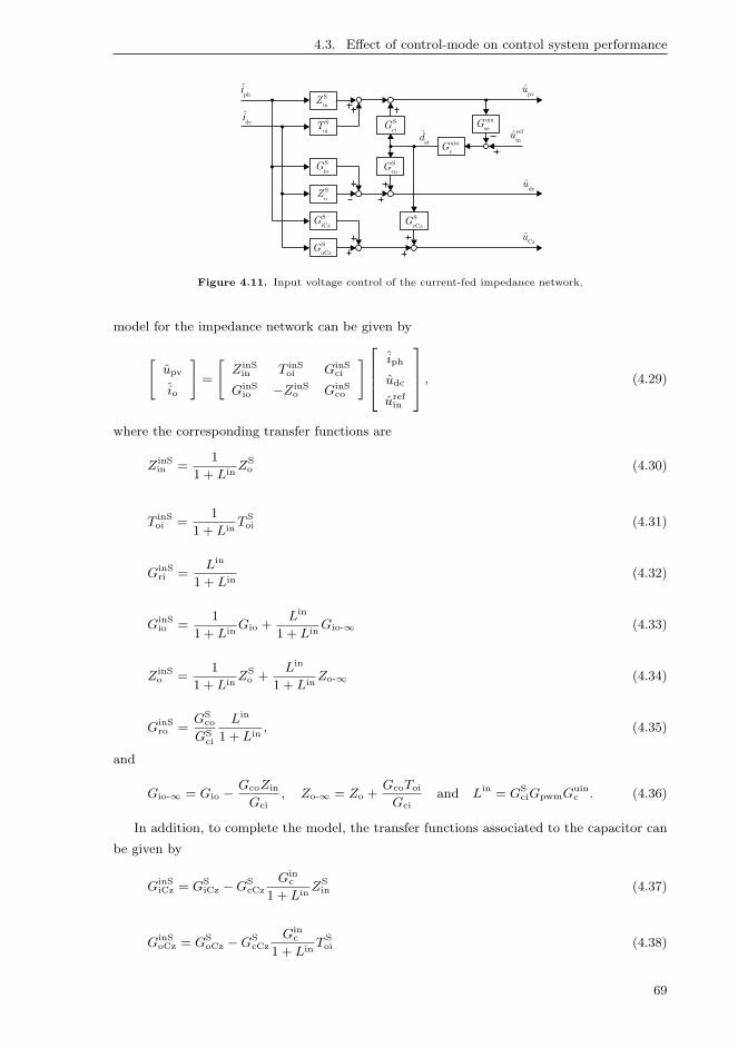
4.3. Effect of control-mode on control system performance
S
inZ
iphˆ
S
oiT
std
dcu
S
ciG
S
oZ
S
ioG
Czu
S
oCzG
S
cCzG
S
iCzG
pvu
idcˆ
uin
seG
uin
cG
ref
inu
S
coG
Figure 4.11. Input voltage control of the current-fed impedance network.
model for the impedance network can be given by
[
upv
io
]
=
[
Z inSin T inS
oi GinSci
GinSio −Z inS
o GinSco
]
iph
udc
urefin
, (4.29)
where the corresponding transfer functions are
Z inSin =
1
1 + LinZS
o (4.30)
T inSoi =
1
1 + LinT Soi (4.31)
GinSri =
Lin
1 + Lin(4.32)
GinSio =
1
1 + LinGio +
Lin
1 + LinGio-∞ (4.33)
Z inSo =
1
1 + LinZS
o +Lin
1 + LinZo-∞ (4.34)
GinSro =
GSco
GSci
Lin
1 + Lin, (4.35)
and
Gio-∞ = Gio −GcoZin
Gci, Zo-∞ = Zo +
GcoToi
Gciand Lin = GS
ciGpwmGuinc . (4.36)
In addition, to complete the model, the transfer functions associated to the capacitor can
be given by
GinSiCz = GS
iCz −GScCz
Ginc
1 + LinZS
in (4.37)
GinSoCz = GS
oCz −GScCz
Ginc
1 + LinT Soi (4.38)
69
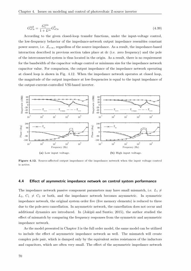
Chapter 4. Issues on modeling and control of photovoltaic Z-source inverter
GinSrCz =
Guinc
1 + LinGS
cCz (4.39)
According to the given closed-loop transfer functions, under the input-voltage control,
the low-frequency behavior of the impedance-network output impedance resembles constant
power source, i.e. Zo-∞, regardless of the source impedance. As a result, the impedance-based
interaction described in previous section takes place at dc (i.e. zero frequency) and the pole
of the interconnected system is thus located in the origin. As a result, there is no requirement
for the bandwidth of the capacitor voltage control or minimum size for the impedance network
capacitor value. For comparison, the output impedance of the impedance network operating
at closed loop is shown in Fig. 4.12. When the impedance network operates at closed loop,
the magnitude of the output impedance at low-frequencies is equal to the input impedance of
the output-current-controlled VSI-based inverter.
10-1
100
101
102
103
-60-40-20
0204060
Mag
nit
ude
(dB
Ω)
Zo-cv
Zo-mpp
Zo-cc
10-1
100
101
102
103
-180
-90
0
90
180
Phas
e (d
eg)
Frequency (Hz)
Zin
(a) Low input voltage.
10-1
100
101
102
103
-60-40-20
0204060
Mag
nit
ude
(dB
Ω)
Zo-cv
Zo-mpp
Zo-cc
10-1
100
101
102
103
-180
-90
0
90
180
Phas
e (d
eg)
Frequency (Hz)
Zin
(b) High input voltage.
Figure 4.12. Source-affected output impedance of the impedance network when the input voltage control
is active.
4.4 Effect of asymmetric impedance network on control system performance
The impedance network passive component parameters may have small mismatch, i.e. L1 6=
L2, C1 6= C2 or both, and the impedance network becomes asymmetric. In symmetric
impedance network, the original system order five (five memory elements) is reduced to three
due to the pole-zero cancellation. In asymmetric network, the cancellation does not occur and
additional dynamics are introduced. In (Jokipii and Suntio; 2015), the author studied the
effect of mismatch by comparing the frequency responses from the symmetric and asymmetric
impedance network.
As the model presented in Chapter 3 is the full order model, the same model can be utilized
to include the effect of asymmetric impedance network as well. The mismatch will create
complex pole pair, which is damped only by the equivalent series resistances of the inductors
and capacitors, which are often very small. The effect of the asymmetric impedance network
70
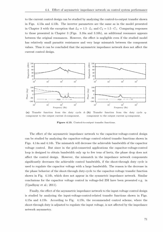
4.4. Effect of asymmetric impedance network on control system performance
to the current control design can be studied by analyzing the control-to-output transfer shown
in Figs. 4.13a and 4.13b. The inverter parameters are the same as in the model presented
in Chapter 3 with the exception that L2 = 1.5 · L1 and C2 = 1.5 · C1. Comparing responses
to those presented in Chapter 3 (Figs. 3.16a and 3.16b), an additional resonance appears
between the original resonances. However, the effect is negligible even if the studied model
has relatively small parasitic resistances and very large mismatch between the component
values. Thus it can be concluded that the asymmetric impedance network does not affect the
current control design.
100
101
102
103
0
20
40
60
80
100
Mag
nit
ude
(dB
A)
100
101
102
103
-180
-90
0
90
180
Phas
e (d
eg)
Frequency (Hz)
cv mpp cc
(a) Transfer function from the duty cycle d-
component to the output current d-component.
100
101
102
103
0
20
40
60
80
100
Mag
nit
ude
(dB
A)
100
101
102
103
-180
-90
0
90
180P
has
e (d
eg)
Frequency (Hz)
cv mpp cc
(b) Transfer function from the duty cycle q-
component to the output current q-component.
Figure 4.13. Control-to-output transfer functions.
The effect of the asymmetric impedance network to the capacitor-voltage-control design
can be studied by analyzing the capacitor-voltage control related transfer functions shown in
Figs. 4.14a and 4.14b. The mismatch will decrease the achievable bandwidth of the capacitor
voltage control. But since in the grid-connected applications the capacitor-voltage-control
loop is designed to obtain bandwidth only up to few tens of hertz, the phase drop does not
affect the control design. However, the mismatch in the impedance network components
significantly decreases the achievable control bandwidth, if the shoot-through duty cycle is
used to regulate the capacitor voltage with a large bandwidth. The reason is the decrease in
the phase behavior of the shoot-through duty-cycle to the capacitor-voltage transfer function
shown in Fig. 4.14b, which does not appear in the symmetric impedance network. Similar
conclusions for the capacitor voltage control in voltage-fed ZSI have been presented e.g. in
(Upadhyay et al.; 2011).
Finally, the effect of the asymmetric impedance network to the input-voltage control design
is studied by analyzing the input-voltage-control-related transfer functions shown in Figs.
4.15a and 4.15b. According to Fig. 4.15b, the recommended control scheme, where the
shoot-through duty is adjusted to regulate the input voltage, is not affected by the impedance
network asymmetry.
71
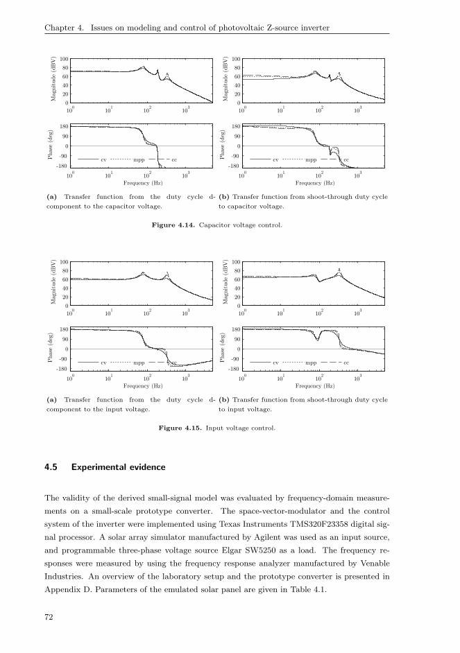
Chapter 4. Issues on modeling and control of photovoltaic Z-source inverter
100
101
102
103
0
20
40
60
80
100M
agnit
ude
(dB
V)
100
101
102
103
-180
-90
0
90
180
Phas
e (d
eg)
Frequency (Hz)
cv mpp cc
(a) Transfer function from the duty cycle d-
component to the capacitor voltage.
100
101
102
103
0
20
40
60
80
100
Mag
nit
ude
(dB
V)
100
101
102
103
-180
-90
0
90
180
Phas
e (d
eg)
Frequency (Hz)
cv mpp cc
(b) Transfer function from shoot-through duty cycle
to capacitor voltage.
Figure 4.14. Capacitor voltage control.
100
101
102
103
0
20
40
60
80
100
Mag
nit
ude
(dB
V)
100
101
102
103
-180
-90
0
90
180
Phas
e (d
eg)
Frequency (Hz)
cv mpp cc
(a) Transfer function from the duty cycle d-
component to the input voltage.
100
101
102
103
0
20
40
60
80
100
Mag
nit
ude
(dB
V)
100
101
102
103
-180
-90
0
90
180
Phas
e (d
eg)
Frequency (Hz)
cv mpp cc
(b) Transfer function from shoot-through duty cycle
to input voltage.
Figure 4.15. Input voltage control.
4.5 Experimental evidence
The validity of the derived small-signal model was evaluated by frequency-domain measure-
ments on a small-scale prototype converter. The space-vector-modulator and the control
system of the inverter were implemented using Texas Instruments TMS320F23358 digital sig-
nal processor. A solar array simulator manufactured by Agilent was used as an input source,
and programmable three-phase voltage source Elgar SW5250 as a load. The frequency re-
sponses were measured by using the frequency response analyzer manufactured by Venable
Industries. An overview of the laboratory setup and the prototype converter is presented in
Appendix D. Parameters of the emulated solar panel are given in Table 4.1.
72
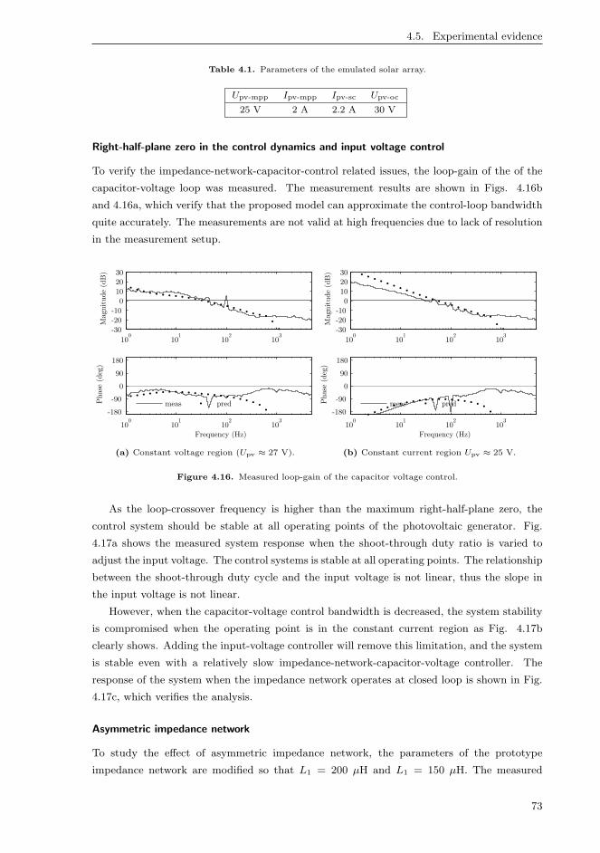
4.5. Experimental evidence
Table 4.1. Parameters of the emulated solar array.
Upv-mpp Ipv-mpp Ipv-sc Upv-oc
25 V 2 A 2.2 A 30 V
Right-half-plane zero in the control dynamics and input voltage control
To verify the impedance-network-capacitor-control related issues, the loop-gain of the of the
capacitor-voltage loop was measured. The measurement results are shown in Figs. 4.16b
and 4.16a, which verify that the proposed model can approximate the control-loop bandwidth
quite accurately. The measurements are not valid at high frequencies due to lack of resolution
in the measurement setup.
100
101
102
103
-30
-20
-10
0
10
20
30
Mag
nit
ude
(dB
)
100
101
102
103
-180
-90
0
90
180
Phas
e (d
eg)
Frequency (Hz)
meas pred
(a) Constant voltage region (Upv ≈ 27 V).
100
101
102
103
-30
-20
-10
0
10
2030
Mag
nit
ude
(dB
)
100
101
102
103
-180
-90
0
90
180
Phas
e (d
eg)
Frequency (Hz)
meas pred
(b) Constant current region Upv ≈ 25 V.
Figure 4.16. Measured loop-gain of the capacitor voltage control.
As the loop-crossover frequency is higher than the maximum right-half-plane zero, the
control system should be stable at all operating points of the photovoltaic generator. Fig.
4.17a shows the measured system response when the shoot-through duty ratio is varied to
adjust the input voltage. The control systems is stable at all operating points. The relationship
between the shoot-through duty cycle and the input voltage is not linear, thus the slope in
the input voltage is not linear.
However, when the capacitor-voltage control bandwidth is decreased, the system stability
is compromised when the operating point is in the constant current region as Fig. 4.17b
clearly shows. Adding the input-voltage controller will remove this limitation, and the system
is stable even with a relatively slow impedance-network-capacitor-voltage controller. The
response of the system when the impedance network operates at closed loop is shown in Fig.
4.17c, which verifies the analysis.
Asymmetric impedance network
To study the effect of asymmetric impedance network, the parameters of the prototype
impedance network are modified so that L1 = 200 µH and L1 = 150 µH. The measured
73

Chapter 4. Issues on modeling and control of photovoltaic Z-source inverter
frequency responses of the system are identical to those presented in Chapter 3 and are not
repeated here. The time-domain measurement, presented in Figs. 4.18a and 4.18b, indicate
that the asymmetric impedance network does not affect the response of the system. Measure-
ments are carried out in the current region of the PVG, since the damping of the system is
lowest in when the PVG dynamic resistance is high. The transient response with the asym-
metric impedance network do not contain any additional oscillation. Moreover, the measured
output impedance presented in Figs. 4.19a and 4.19b, verifies the accuracy of the closed-loop
model with the control loops and the asymmetric impedance network.
4.6 Conclusions
This chapter discussed the control design of a grid-connected photovoltaic Z-source inverter.
According to the presented analysis, the control of the inverter should be based on regulat-
ing the input voltage by using the shoot-through duty cycle, and the impedance-network-
capacitor-voltage control should be implemented by using the conventional cascade control,
where the high bandwidth current forms the innermost loop. To improve the dynamic perfor-
mance, the input voltage of the converter should be regulated by adjusting the shoot-through
duty cycle. The validity of the analysis was verified by means of laboratory measurements. It
was shown that the proposed model can predict the loop gain of the capacitor-voltage-control
loop and if the control bandwidth is decreased the instability associated with the right-half-
plane zero will cause undesired oscillations. In addition, the measurements carried out with
the inverter equipped with an asymmetric impedance network verify that the mismatches in
the impedance network parameters do not compromise the stability of the system or affect
the transient response.
74

4.6. Conclusions
in(5V / div)u
Cz(5V / div)u
o-a(2A / div)i
(a) Input voltage sweep when the impedance network operates in open-loop and the control design
satisfies the design criteria given.
in(5V / div)u
Cz(5V / div)u
o-a(2A / div)i
(b) Input voltage sweep when the impedance network operates in open-loop and the control
design does not satisfy the design criteria given.
in(5V / div)u
Cz(5V / div)u
o-a(2A / div)i
(c) Input voltage sweep when the impedance network operates in closed-loop. Same impedance
network capacitor voltage controller as in Fig. 4.17b is used.
Figure 4.17. Input voltage sweep.
75
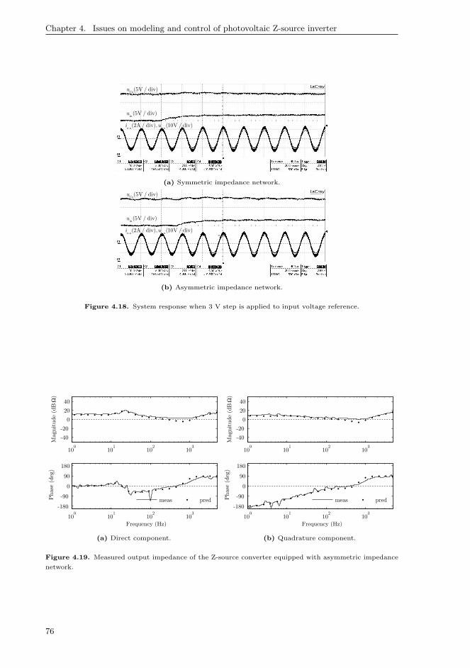
Chapter 4. Issues on modeling and control of photovoltaic Z-source inverter
in(5V / div)u
Cz(5V / div)u
o-a o-a(2A / div), (10V / div)i u
(a) Symmetric impedance network.
zo_d.dat
in(5V / div)u
Cz(5V / div)u
o-a o-a(2A / div), (10V / div)i u
(b) Asymmetric impedance network.
Figure 4.18. System response when 3 V step is applied to input voltage reference.
100
101
102
103
-40
-20
0
20
40
Mag
nit
ude
(dB
Ω)
100
101
102
103
-180
-90
0
90
180
Phas
e (d
eg)
Frequency (Hz)
meas pred
(a) Direct component.
100
101
102
103
-40
-20
0
20
40
Mag
nit
ude
(dB
Ω)
100
101
102
103
-180
-90
0
90
180
Phas
e (d
eg)
Frequency (Hz)
meas pred
(b) Quadrature component.
Figure 4.19. Measured output impedance of the Z-source converter equipped with asymmetric impedance
network.
76

5 COMPARISON OF DYNAMIC CHARACTERISTICS OF VSI
AND ZSI-BASED PV INVERTERS
In this chapter, the similarities and differences between the dynamic properties of ZSI and
VSI-based inverter are discussed. The comparison is carried out by utilizing the small-signal
models presented in the previous chapters of this thesis.
5.1 Appearance of RHP zero in dynamics
Current-fed single and two-stage VSI-based inverters and the current-fed Z-source inverter
incorporates a low-frequency right-half-plane zero in the control related transfer functions.
The zero must be taken into account in the control design and it determines also the minimum
size for the capacitor in the dc-link of the VSI-based inverter or impedance network capacitor
in Z-source inverter.
In grid-connected applications, the minimum dc-link voltage of a VSI-based inverter and
the minimum impedance network capacitor voltage of a Z-source inverter are dictated by the
grid voltage. The voltage at the dc-side of the inverter-bridge must be higher than the peak
value of the line voltage with a sufficient margin. In the two-stage VSI-based inverter and Z-
source inverter, the inverter input voltage, i.e. the PVG voltage, can be regulated to a lower
value than this limit by utilizing the two-stage inverter boost-stage or Z-source impedance
network.
Voltage-boost mode
When the boost stage of the current-fed two-stage VSI-based inverter is operated at open loop,
the right-half plane zero associated to the control dynamics can be given as (Messo et al.;
2014):
ωrhp ≈Ppv
CdcU2dc
(5.1)
According to results presented in Chapter 4, the right-half plane zero of the current-fed
Z-source inverter can be given as:
ωrhp ≈Ppv
CinU2pv + 2C1U2
Cz
(5.2)
However, as discussed in Chapter 4, the input capacitor has very small contribution to the
maximum zero frequency when the input voltage is low, since U2pv << 2U2
Cz, which indicates
77

Chapter 5. Comparison of dynamic characteristics of VSI and ZSI-based PV inverters
that
ωrhp ≈Ppv
2C1U2Cz
(5.3)
According to (5.1) and (5.3), the RHP-zero frequencies of the two-stage VSI and the ZSI
are the same if the same amount of capacitance is connected to the dc-link or in the impedance
network. Thus the small-signal stability of the Z-source inverter can be guaranteed by using
the same equation with the exception that both impedance network capacitors contributes.
The most critical condition occurs at the maximum power point.
When the aforementioned inverters are operated at closed loop, i.e., under input voltage
control, the zero moves from right-half-plane to origin. As a consequence, there are then
no requirements for the dc-link voltage control or the impedance network capacitor voltage
control to stabilize the system.
Voltage-buck mode
In VSI-based single-stage inverter operating in buck mode, the frequency of the zero equals
ωrhp =Idc
CdcUdc(5.4)
When the two-stage inverter is operated in the buck-mode and the boost stage is shorted
or its duty ratio is set to zero, the capacitors associated to the boost converter increases the
equivalent capacitance connected to the dc-link. Accordingly, when the Z-source inverter is
operated in the buck-mode, i.e. when the boost stage is shorted or its duty ratio is set to
zero, the capacitors associated with the boost converter increases the equivalent capacitance
connected to the dc-link. The maximum limit given by the (5.4) is sufficient to guarantee small-
signal stability. The most critical condition occurs at minimum input voltage and maximum
input current.
5.2 Output impedance
The interaction of the grid-connected inverter and the utility grid can be analyzed by using the
output impedance of the inverter. As the inverter stage and the grid-current control scheme of
the Z-source inverter and the single and two-stage VSI-based inverters are similar, it is quite
natural that the output impedance of the Z-source inverter resembles the output impedance
of the VSI-based inverter. (Jokipii et al.; 2014) (Messo et al.; 2013)
The actual shape of the output impedance of the VSI-based inverter including all the
control loops can be predicted by using the model presented in Chapter 2. An example of the
single-stage-inverter output impedance operated at open loop is presented in Fig. 5.1. The
shape of the impedance is similar to the output impedance of the Z-source inverter shown in
Fig. 5.2, which can be predicted by using the model presented in Chapter 4.
The additional high-frequency resonance in Figs. 5.1 - 5.1 originates from the impedance
network characteristics. When the impedance network is operated at open loop, the series
resonance associated to the impedance network affects the current control of the inverter. The
78
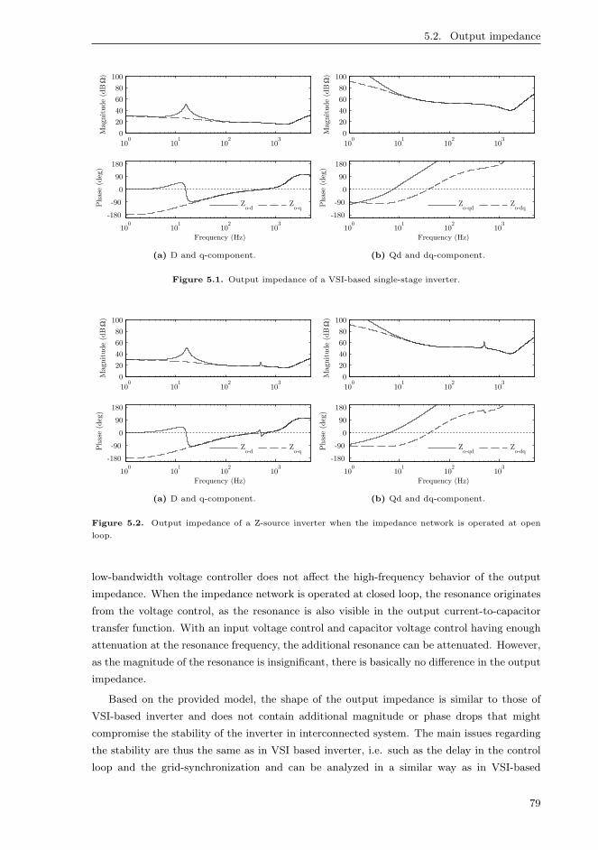
5.2. Output impedance
100
101
102
103
0
20
40
60
80
100
Mag
nit
ude
(dB
Ω)
100
101
102
103
-180
-90
0
90
180
Phas
e (d
eg)
Frequency (Hz)
Zo-d
Zo-q
(a) D and q-component.
100
101
102
103
0
20
40
60
80
100
Mag
nit
ude
(dB
Ω)
100
101
102
103
-180
-90
0
90
180
Phas
e (d
eg)
Frequency (Hz)
Zo-qd
Zo-dq
(b) Qd and dq-component.
Figure 5.1. Output impedance of a VSI-based single-stage inverter.
100
101
102
103
0
20
40
60
80
100
Mag
nit
ude
(dB
Ω)
100
101
102
103
-180
-90
0
90
180
Phas
e (d
eg)
Frequency (Hz)
Zo-d
Zo-q
(a) D and q-component.
100
101
102
103
0
20
40
60
80
100M
agnit
ude
(dB
Ω)
100
101
102
103
-180
-90
0
90
180
Phas
e (d
eg)
Frequency (Hz)
Zo-qd
Zo-dq
(b) Qd and dq-component.
Figure 5.2. Output impedance of a Z-source inverter when the impedance network is operated at open
loop.
low-bandwidth voltage controller does not affect the high-frequency behavior of the output
impedance. When the impedance network is operated at closed loop, the resonance originates
from the voltage control, as the resonance is also visible in the output current-to-capacitor
transfer function. With an input voltage control and capacitor voltage control having enough
attenuation at the resonance frequency, the additional resonance can be attenuated. However,
as the magnitude of the resonance is insignificant, there is basically no difference in the output
impedance.
Based on the provided model, the shape of the output impedance is similar to those of
VSI-based inverter and does not contain additional magnitude or phase drops that might
compromise the stability of the inverter in interconnected system. The main issues regarding
the stability are thus the same as in VSI based inverter, i.e. such as the delay in the control
loop and the grid-synchronization and can be analyzed in a similar way as in VSI-based
79
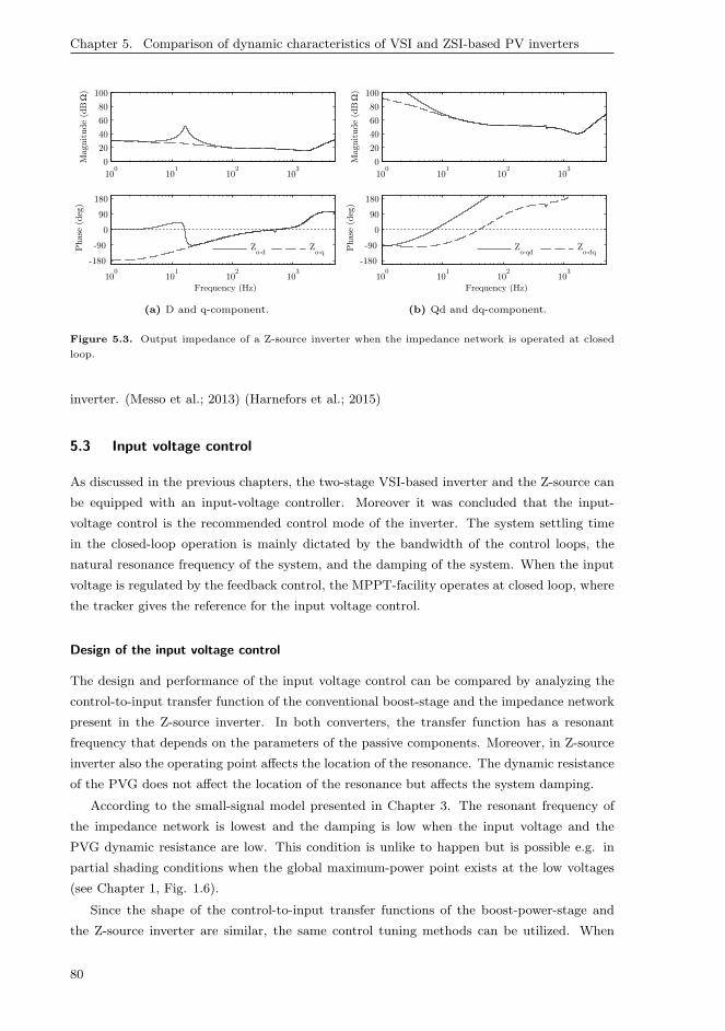
Chapter 5. Comparison of dynamic characteristics of VSI and ZSI-based PV inverters
100
101
102
103
0
20
40
60
80
100M
agnit
ude
(dB
Ω)
100
101
102
103
-180
-90
0
90
180
Phas
e (d
eg)
Frequency (Hz)
Zo-d
Zo-q
(a) D and q-component.
100
101
102
103
0
20
40
60
80
100
Mag
nit
ude
(dB
Ω)
100
101
102
103
-180
-90
0
90
180
Phas
e (d
eg)
Frequency (Hz)
Zo-qd
Zo-dq
(b) Qd and dq-component.
Figure 5.3. Output impedance of a Z-source inverter when the impedance network is operated at closed
loop.
inverter. (Messo et al.; 2013) (Harnefors et al.; 2015)
5.3 Input voltage control
As discussed in the previous chapters, the two-stage VSI-based inverter and the Z-source can
be equipped with an input-voltage controller. Moreover it was concluded that the input-
voltage control is the recommended control mode of the inverter. The system settling time
in the closed-loop operation is mainly dictated by the bandwidth of the control loops, the
natural resonance frequency of the system, and the damping of the system. When the input
voltage is regulated by the feedback control, the MPPT-facility operates at closed loop, where
the tracker gives the reference for the input voltage control.
Design of the input voltage control
The design and performance of the input voltage control can be compared by analyzing the
control-to-input transfer function of the conventional boost-stage and the impedance network
present in the Z-source inverter. In both converters, the transfer function has a resonant
frequency that depends on the parameters of the passive components. Moreover, in Z-source
inverter also the operating point affects the location of the resonance. The dynamic resistance
of the PVG does not affect the location of the resonance but affects the system damping.
According to the small-signal model presented in Chapter 3. The resonant frequency of
the impedance network is lowest and the damping is low when the input voltage and the
PVG dynamic resistance are low. This condition is unlike to happen but is possible e.g. in
partial shading conditions when the global maximum-power point exists at the low voltages
(see Chapter 1, Fig. 1.6).
Since the shape of the control-to-input transfer functions of the boost-power-stage and
the Z-source inverter are similar, the same control tuning methods can be utilized. When
80
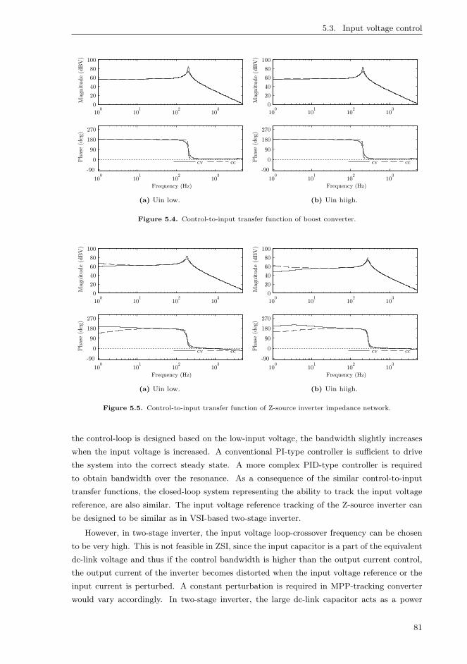
5.3. Input voltage control
100
101
102
103
0
20
40
60
80
100
Mag
nit
ude
(dB
V)
100
101
102
103
-90
0
90
180
270
Phas
e (d
eg)
Frequency (Hz)
cv cc
(a) Uin low.
100
101
102
103
0
20
40
60
80
100
Mag
nit
ude
(dB
V)
100
101
102
103
-90
0
90
180
270
Phas
e (d
eg)
Frequency (Hz)
cv cc
(b) Uin hiigh.
Figure 5.4. Control-to-input transfer function of boost converter.
100
101
102
103
0
20
40
60
80
100
Mag
nit
ude
(dB
V)
100
101
102
103
-90
0
90
180
270
Phas
e (d
eg)
Frequency (Hz)
cv cc
(a) Uin low.
100
101
102
103
0
20
40
60
80
100M
agnit
ude
(dB
V)
100
101
102
103
-90
0
90
180
270
Phas
e (d
eg)
Frequency (Hz)
cv cc
(b) Uin hiigh.
Figure 5.5. Control-to-input transfer function of Z-source inverter impedance network.
the control-loop is designed based on the low-input voltage, the bandwidth slightly increases
when the input voltage is increased. A conventional PI-type controller is sufficient to drive
the system into the correct steady state. A more complex PID-type controller is required
to obtain bandwidth over the resonance. As a consequence of the similar control-to-input
transfer functions, the closed-loop system representing the ability to track the input voltage
reference, are also similar. The input voltage reference tracking of the Z-source inverter can
be designed to be similar as in VSI-based two-stage inverter.
However, in two-stage inverter, the input voltage loop-crossover frequency can be chosen
to be very high. This is not feasible in ZSI, since the input capacitor is a part of the equivalent
dc-link voltage and thus if the control bandwidth is higher than the output current control,
the output current of the inverter becomes distorted when the input voltage reference or the
input current is perturbed. A constant perturbation is required in MPP-tracking converter
would vary accordingly. In two-stage inverter, the large dc-link capacitor acts as a power
81

Chapter 5. Comparison of dynamic characteristics of VSI and ZSI-based PV inverters
buffer and similar behavior does not take place. The main drawback of the Z-source inverter
in comparison to the two-stage inverter is thus the requirement for the location of the sys-
tem resonance. The resonance should be limited to lower than the output current control
bandwidth with a sufficient margin.
5.4 Conclusions
The dynamics of the VSI-based inverters and the Z-source inverter contains a low frequency
right-half-plane zero in the control-related transfer functions. The zero must be taken into
account in the dc-link voltage control and in the impedance-network-capacitor-voltage control.
It was shown that the design rule previously derived for selection of the two-stage VSI-based
inverter dc-link capacitance can be also utilized in Z-source inverter. In addition, it was shown
that the input-voltage control design can be carried out in a similar way as in the two-stage
VSI-based inverter and the similar control performance can be obtained. Finally, it was shown
that the shape of the output impedance of the Z-source inverter and the VSI-based inverter
are similar.
82
6 CONCLUSIONS
6.1 Final conclusions
As concluded by several research groups, the three-phase Z-source inverter is suitable for
interfacing of a photovoltaic power generator into the utility grid. However, the dynamic
characteristics of the converter is often analyzed without taking into account the effect of the
real source behavior, which may hide important details about the system stability and per-
formance under varying operating conditions such as in the photovoltaic applications where
the PV-generator impedance varies according to the operating point. This thesis presented
an accurate modeling method to evaluate the dynamic characteristics of the Z-source inverter,
discussed the issues related to the control of the inverter, and finally compared several char-
acteristics of the Z-source inverter to those of the conventional VSI-based inverter. In terms
of dynamic characteristics, there seem to be no major disadvantages (or advantages) in ZSI
over the traditional photovoltaic inverter.
In Chapters 2 and 3, a consistent method to model the dynamic characteristics of the
three-phase grid-connected Z-source inverter was presented. The analysis was carried out by
developing an accurate small-signal model for the inverter, which was used to highlight the
differences between the dynamics of a voltage-fed and a current-fed Z-source inverter and
further developed to model the photovoltaic inverter. The voltage-fed model was shown to
present the characteristics of a photovoltaic inverter incorrectly. Thus to capture the dynamics
correctly and to include all the control loops, the photovoltaic Z-source should be analyzed as
a current-fed system and the effect of the photovoltaic generator was included by using the
proposed source-affected model.
According to Chapter 4, the control of the photovoltaic Z-source inverter should be based
on regulating the input voltage of the converter by adjusting the length of the shoot-through
state, and the impedance network capacitor voltage control should be implemented using
cascade controlled output current control, where the slow capacitor-voltage control adjusts the
reference of the fast output current control. When the converter operates under feedback from
the input voltage, the right-half-plane zero associated to the output-current control disappears.
Without the input voltage control, the stability of the inverter may be compromised. In
addition, it was shown in Chapter 4 that the small mismatch in the impedance network
parameters causes additional resonances in the system but does not compromise the stability
and performance of the inverter.
In Chapter 5, the characteristics of a Z-source inverter was compared to VSI based inverter.
83
Chapter 6. Conclusions
The previously published method to determine the minimum capacitance required in the dc-
link of the two-stage inverter was shown to be similar to the limit proposed for the Z-source
inverter in Chapter 4. The output impedance of a Z-source inverter resembles the output
impedance of a conventional inverters. In addition, the input-voltage-control bandwidth can
be designed to be similar as in two-stage VSI-based inverter, which provides a sufficient
maximum-power-point tracking performance.
6.2 Future topics
The author’s recommendations for the future topics regarding the research of a Z-source
inverter include:
• The output current control bandwidth varies as a function of the equivalent dc-link
voltage. As a result, the output current control performance and thus the shape of the
output impedance varies as a function of the input voltage of the inverter. In ideal case,
the current control is not affected by the voltage level. The effect of gain scheduling
together, which is usually indirectly included by using the space-vector pulse-width
modulation, effect should be studied.
• The impedance network of the Z-source inverter contains reactive elements and an os-
cillating energy transfer will occur between the components in certain conditions. The
phenomenon is amplified if there is mismatch in the impedance network parameters. In
this work, a high-bandwidth-input-voltage control can be used to damp the oscillation.
A need for more sophisticated damping (e.g. current control in impedance network)
should be studied.
• The impedance network inductor can be wound on the same core. The effect of the
coupling on the dynamics should be included in the model.
• Main differences between the dynamic-characteristics of quazi-ZSI and other derived
topologies, should be studied.
• In this thesis, only MPPT operation was discussed. However, the converter may oper-
ate also in the power limiting mode, i.e., when the voltage-control current reference is
saturated. This is a natural result of a downsized inverter. This is actually a property
of a MPP-tracking converter also, since it is very customary to downsize the inverter in
respect to the PVG power. The inverter operating in power limiting mode basically has
only current control. Inverter works fine if the PVG operating point of the inverter is
in voltage region but becomes unstable when the operating point moves to the current
region.
84
REFERENCES
Anderson, J. and Peng, F. Z. (2008). Four quasi-Z-source inverters, IEEE Power Electronics
Specialists Conf. (PESC’08), pp. 2743–2749.
Araujo, S. V., Zacharias, P. and Mallwitz, R. (2010). Highly efficient single-phase trans-
formerless inverters for grid-connected photovoltaic systems, IEEE Trans. Ind. Electron.
57(9): 3118–3128.
Blaabjerg, F., Chen, Z. and Kjaer, S. B. (2004). Power electronics as efficient interface in
dispersed power generation systems, IEEE Trans. Power Electron. 19(5): 1184–1194.
Blaabjerg, F., Teodorescu, R., Liserre, M. and Timbus, A. V. (2006). Overview of control and
grid synchronization for distributed power generation systems, IEEE Trans. Ind. Electron.
53(5): 1398–1409.
Bose, B. K. (2013). Global energy scenario and impact of power electronics in 21st century,
IEEE Trans. Ind. Electron. 60(7): 2638–2651.
Bradaschia, F., Cavalcanti, M. C., Ferraz, P. E. P., Neves, F. A. S., dos Santos, E. C. and
da Silva, J. H. G. M. (2011). Modulation for three-phase transformerless Z-source inverter to
reduce leakage currents in photovoltaic systems, IEEE Trans. Ind. Electron. 58(12): 5385–
5395.
Buso, S. and Mattavelli, P. (2006). Digital Control in Power Electronics, Morgan & Claypool
Publishers.
Carrasco, J. M., Franquelo, L. G., Bialasiewicz, J. T., Member, S., Galvan, E., Guisado,
R. C. P., Member, S., Angeles, M., Prats, M., Leon, J. I. and Moreno-alfonso, N. (2006).
Power-electronic systems for the grid integration of renewable energy sources: a survey,
IEEE Trans. Ind. Electron. 53(4): 1002–1016.
Chatterjee, A., Member, S., Keyhani, A. and Kapoor, D. (2011). Identification of photovoltaic
source models, IEEE Trans. Energy Convers. 26(3): 883–889.
de Brito, M., Galotto, L., Sampaio, L. P., de Azevedo e Melo, G. and Canesin, C. A. (2013).
Evaluation of the main MPPT techniques for photovoltaic applications, IEEE Trans. Ind.
Electron. 60(3): 1156–1167.
85

References
Ding, K., Bian, X., Liu, H. and Peng, T. (2012). A MATLAB-Simulink-based PV module
model and its application under conditions of nonuniform irradiance, IEEE Trans. Energy
Convers. 27(4): 864–872.
Divan, D., Moghe, R. and Prasai, A. (2014). Power electronics at the grid edge: the key to
unlocking value from the smart grid, IEEE Power Electron. Magazine 1(4): 16–22.
Enslin, J. H. R. and Heskes, P. J. M. (2004). Harmonic interaction between a large number
of distributed power inverters and the distribution network, IEEE Trans. Power Electron.
19(6): 1586–1593.
Femia, N., Lisi, G., Petrone, G., Spagnuolo, G. and Vitelli, M. (2008). Distributed maximum
power point tracking of photovoltaic arrays: novel approach and system analysis, IEEE
Trans. Ind. Electron. 55(7): 2610–2621.
Femia, N., Petrone, G., Spagnuolo, G. and Vitelli, M. (2009). A technique for improving P&O
MPPT performances of double-stage grid-connected photovoltaic systems, IEEE Trans. Ind.
Electron. 56(11): 4473–4482.
Gajanayake, C. J., Vilathgamuwa, D. and Loh, P. C. (2007). Development of a comprehen-
sive model and a multiloop controller for z-source inverter dg systems, IEEE Trans. Ind.
Electron. 54(4): 2352–2359.
Gajanayake, C. J., Vilathgamuwa, D. M. and Loh, P. C. (2005). Small-signal and signal-flow-
graph modeling of switched Z-source impedance network, IEEE Trans. Power Electron.
3(3): 111–116.
Gajanayake, C. J., Vilathgamuwa, D. M., Member, S., Loh, P. C., Teodorescu, R. and Blaab-
jerg, F. (2009). Z-source-inverter-based flexible distributed generation system solution for
grid power quality improvement, IEEE Trans. Energy Convers. 24(3): 695–704.
Galigekere, V. P. and Kazimierczuk, M. K. (2013). Small-signal modeling of open-loop
PWM Z-source converter by circuit-averaging technique, IEEE Trans. Power Electron.
28(3): 1286–1296.
Gao, F., Loh, P. C., Blaabjerg, F. and Gajanayake, C. J. (2008). Operational analysis and
comparative evaluation of embedded Z-source inverters, IEEE Power Electronics Specialists
Conference (PESC’08), pp. 2757–2763.
Gao, F., Loh, P. C., Teodorescu, R. and Blaabjerg, F. (2009). Diode-assisted buck–boost
voltage-source inverters, IEEE Trans. Power Electron. 24(9): 2057–2064.
Gao, L., Dougal, R. A., Liu, S. and Iotova, A. P. (2009). Parallel-connected solar PV system
to address partial and rapidly fluctuating shadow conditions, IEEE Trans. Ind. Electron.
56(5): 1548–1556.
Gataric, S. and Garrigan, N. R. (1999). Modeling and design of three-phase systems using
complex transfer functions, IEEE Power Electronics Specialists Conference (PESC’99).
86
References
Hanif, M., Basu, M. and Gaughan, K. (2011). Understanding the operation of a Z-source in-
verter for photovoltaic application with a design example, IET Power Electronics 4(3): 278.
Harnefors, L. (2007). Modeling of three-phase dynamic systems using complex transfer func-
tions and transfer matrices, IEEE Trans. Ind. Electron. 54(4): 2239–2248.
Harnefors, L., Yepes, A. G., Vidal, A. and Doval-gandoy, J. (2015). Passivity-based controller
design of grid-connected VSCs for prevention of electrical resonance instability, IEEE Trans.
Ind. Electron. 62(2): 702–710.
Hiti, S. and Boroyevich, D. (1996). Small-signal modeling of three-phase PWM modulators,
IEEE Electronics Specialists Conference (PESC’96), Vol. 1, pp. 550–555.
Huang, Y., Shen, M., Peng, F. Z. and Wang, J. (2006). Z-source inverter for residential
photovoltaic systems, IEEE Trans. Power Electron. 21(6): 1776–1782.
International Energy Agency (2015). Snapshot of global PV markets 2014, Technical report.
URL: http://www.iea-pvps.org/ [Date accessed: 5.3.2013]
Jokipii, J., Messo, T. and Suntio, T. (2013). Input voltage control of a three-phase Z-source
inverter in photovoltaic applications, IEEE Symposium on Power Electronics for Distributed
Generation Systems (PEDG), pp. 1–8.
Jokipii, J., Messo, T. and Suntio, T. (2014). Simple method for measuring output impedance
of a three-phase inverter in dq-domain, IEEE International Power Electronics Conference
(ECCE-ASIA), pp. 1466–1470.
Jokipii, J. and Suntio, T. (2015). Dynamic characteristics of three-phase Z-source-based
photovoltaic inverter with asymmetric impedance network, IEEE Conference on Power
Electronics (ECCE Asia), pp. 1976–1983.
Kikuchi, J. and Lipo, T. A. (2002). Three-phase PWM boost – buck rectifiers with power-
regenerating capability, IEEE Trans. Ind. Appl. 38(5): 1361–1369.
Kjaer, S. B. (2012). Evaluation of the “Hill Climbing” and the “Incremental Conductance”
maximum power point trackers for photovoltaic power systems, IEEE Trans. Energy Con-
vers. 27(4): 922–929.
Kjaer, S. B., Pedersen, J. K. and Blaabjerg, F. (2005). A review of single-phase grid-connected
inverters for photovoltaic modules, IEEE Trans. Ind. Appl. 41(5): 1292–1306.
Kouro, S., Leon, J. I., Vinnikov, D. and Franquelo, L. G. (2015). Grid-connected photovoltaic
systems: an overview of recent research and emerging PV converter technology, IEEE Ind.
Electron. Mag. 9(1): 47–61.
Krein, P. T., Bentsman, J., Bass, R. M. and Lesieutre, B. C. (1989). On the use of averaging
for the analysis of power electronic systems, Computer Engineering (1): 463–467.
87

References
Lavado Villa, L. F., Ho, T.-P., Crebier, J.-C. and Raison, B. (2013). A power electronics
equalizer application for partially shaded photovoltaic modules, IEEE Trans. Ind. Electron.
60(3): 1179–1190.
Li, Y., Jiang, S., Cintron-Rivera, J. G. and Peng, F. Z. (2013). Modeling and control of
quasi-Z-source inverter for distributed generation applications, IEEE Trans. Ind. Electron.
60(4): 1532–1541.
Li, Y., Peng, F. Z., Cintron-Rivera, J. G. and Jiang, S. (2010). Controller design for quasi-Z-
source inverter in photovoltaic systems, IEEE Energy Conversion Congress and Exposition
(ECCE), pp. 3187–3194.
Liserre, M., Sauter, T. and Hung, J. Y. (2010). Future energy systems: Inegrating renewable
energy into the smart power grid through industrial electronics, IEEE Ind. Electron. Mag.
4(March): 18–37.
Liu, J., Hu, J. and Xu, L. (2007). Dynamic modeling and analysis of Z source converter
— derivation of ac small signal model and design-oriented analysis, IEEE Trans. Power
Electron. 22(5): 1786–1796.
Liu, Y., Ge, B., Abu-Rub, H. and Peng, F. Z. (2013). Control system design of vattery-assisted
quasi-Z-source inverter for grid-tie photovoltaic power generation, IEEE Transactions on
Sustainable Energy 4(4): 994–1001.
Liu, Y., Ge, B., Abu-Rub, H. and Peng, F. Z. (2014). Overview of space vector modulations for
three-phase Z-source/quasi-Z-source inverters, IEEE Trans. Power Electron. 29(4): 2098–
2108.
Liu, Y., Haitham, A. R. and Ge, B. (2014). Z-source/quasi-Z-source inverters, IEEE Ind.
Electron. Mag. 8(4): 32–44.
Loh, P., Blaabjerg, F., Feng, S. and Soon, K. (2006). Pulse-width modulated Z-source neutral-
point-clamped inverter, IEEE Applied Power Electronics Conference and Exposition (APEC
’06) pp. 431–437.
Loh, P. C., Li, D. L. and Blaabjerg, F. (2013). Γ-Z-source Inverters, IEEE Trans. Power
Electron. 44(6): 9–10.
Loh, P. C., Lim, S. W., Gao, F. and Blaabjerg, F. (2007). Three-level Z-source inverters using
a single LC impedance network, IEEE Trans. Power Electron. 22(2): 706–711.
Loh, P. C., Vilathgamuwa, D. M., Gajanayake, C. J., Lim, Y. R. and Teo, C. W. (2007).
Transient modeling and analysis of pulse-width modulated Z-source inverter, IEEE Trans.
Ind. Appl. 22(2): 498–507.
Loh, P. C., Vilathgamuwa, D. M., Gajanayake, C. J., Wong, L. T. and Ang, C. P. (2007). Z
-Source current-type inverters : digital modulation and logic implementation, IEEE Trans.
Power Electron. 22(1): 169–177.
88

References
Loh, P. C., Vilathgamuwa, D. M., Lai, Y. S., Chua, G. T. and Li, Y. (2005). Pulse-width
modulation of Z-source inverters, IEEE Trans. Power Electron. 20(6): 1346–1355.
Luoma, J., Kleissl, J. and Murray, K. (2012). Optimal inverter sizing considering cloud
enhancement, Solar Energy 86(1): 421–429.
Mattavelli, P., Mattavelli, P., Stankovic, a. M., Stankovic, a. M., C, G., C, G., Verghese and
Verghese (1999). SSR analysis with dynamic phasor model of thyristor controlled series
capacitor, IEEE Trans. Power Sys. 14(1): 200–208.
Meneses, D., Blaabjerg, F., Garcia, O. and Cobos, J. A. (2013). Review and comparison of
step-up transformerless, IEEE Trans. Power Electron. 28(6): 2649–2663.
Messo, T., Aapro, A. and Suntio, T. (2015). Generalized multivariable small-signal model of
three-phase grid-connected inverter in dq-domain, Workshop on Control and Modeling for
Power Electronics (COMPEL), pp. 1–8.
Messo, T., Jokipii, J., Puukko, J. and Suntio, T. (2014). Determining the value of DC-link
capacitance to ensure stable operation of a three-phase photovoltaic inverter, IEEE Trans.
Power Electron. 29(2): 665–673.
Messo, T., Jokipii, J. and Suntio, T. (2013). Modeling the grid synchronization induced
negative-resistor-like behavior in the output impedance of a three-phase photovoltaic in-
verter, IEEE International Symposium on Power Electronics for Distributed Generation
Systems (PEDG), pp. 1–7.
Middlebrook, R. (1988). Small-signal modeling of pulse-width modulated switched-mode
power converters, Proceedings of the IEEE 76(4): 343–354.
Middlebrook, R. and Cuk, S. (1977). A general unified approach to modelling switching-
converter power stages, International Journal of Electronics 42(6): 512–550.
Nguyen, T. and Low, K. (2010). A global maximum power point tracking scheme employing
direct search algorithm for photovoltaic systems, IEEE Trans. Ind. Electron. 57(10): 3456–
3467.
Nousiainen, L., Puukko, J., Maki, A., Messo, T., Huusari, J., Jokipii, J., Viinamaki, J.,
Lobera, D. T., Valkealahti, S. and Suntio, T. (2013). Photovoltaic generator as an input
source for power electronic converters, IEEE Trans. Power Electron. 28(6): 3028–3038.
Peng, F. Z. (2002). Z-source inverter, IEEE Ind. Appl. Conf., pp. 775–781.
Peng, F. Z. (2003). Z-source inverter, IEEE Trans. Ind. Appl. 39(2): 504–510.
Peng, F. Z., Shen, M. and Qian, Z. (2005). Maximum boost control of the Z-source inverter,
IEEE Trans. Power Electron. 20(4): 833–838.
89

References
Puukko, J., Nousiainen, L. and Suntio, T. (2012). Three-phase photovoltaic inverter small-
signal modelling and model verification, International Conference on Power Electronics,
Machines and Drives (PEMD), pp. 1–6.
Puukko, J. and Suntio, T. (2012). Dynamic properties of a voltage source inverter-based three-
phase inverter in photovoltaic application, IET Renewable Power Generation 6(6): 381–391.
Qian, W., Peng, F. Z. and Cha, H. (2011). Trans-Z-source inverters, IEEE Trans. Power
Electron. 26(12): 3453–3463.
Rajakaruna, S. and Jayawickrama, L. (2010). Steady-state analysis and designing impedance
network of Z-source inverters, IEEE Trans. Ind. Electron. 57(7): 2483–2491.
Romero-Cadaval, E., Spagnuolo, G., Franquelo, L. G., Ramos-Paja, C. A., Suntio, T. and
Xiao, W. M. (2013). Grid-connected photovoltaic generation plants: Components and
operation, IEEE Ind. Electron. Mag. 7(September): 6–20.
Sangwongwanich, A., Yang, Y. and Blaabjerg, F. (2015). High-performance constant power
generation in grid-connected PV systems, IEEE Trans. Power Electron. 8993(99): 1–4.
Shen, M., Wang, J., Joseph, A., Peng, F. Z., Tolbert, L. M. and Adams, D. J. (2006). Constant
boost control of the Z -Source inverter to minimize current ripple and voltage stress, IEEE
Trans. Ind. Appl. 42(3): 770–778.
Siwakoti, Y., Blaabjerg, F. and Loh, P. C. (2015). New magnetically coupled impedance (Z-)
source networks, IEEE Trans. Power Electron. 8993(c): 1–1.
Siwakoti, Y. P., Peng, F. Z., Blaabjerg, F., Loh, P. C. and Town, G. E. (2015). Impedance-
source networks for electric power conversion part I: a topological review, IEEE Trans.
Power Electron. 30(2): 699–716.
Skogestad, S. and Postlethwaite, I. (2005). Multivariable Feedback Control: Analysis and
Design, Wiley.
Sun, J. (2009). Small-signal methods for ac distributed power systems – a review, IEEE Trans.
Power Electron. 24(11): 2545–2554.
Sun, J. (2011). Impedance-based stability criterion for grid-connected inverters, IEEE Trans.
Power Electron. 26(11): 3075–3078.
Suntio, T., Leppaaho, J. and Huusari, J. (2009). Issues on solar-generator-interfacing with
voltage-fed converter, Industrial Electronics (IECON ’09), IEEE, pp. 595–600.
Suntio, T., Leppaaho, J., Huusari, J. and Nousiainen, L. (2010). Issues on solar-
generator interfacing with current-fed MPP-tracking converters, IEEE Trans. Power Elec-
tron. 25(9): 2409–2419.
90

References
Suntio, T., Viinamaki, J., Jokipii, J., Messo, T. and Kuperman, A. (2014). Dynamic charac-
terization of power electronics interfaces, IEEE Trans. Emerg. Sel. Topics Power Electron.
6777(c): 1–1.
Tang, Y., Wei, J. and Xie, S. (2010). A new direct peak DC-link voltage control strategy of
Z-source inverters, IEEE Applied Power Electronics Conference and Exposition (APEC),
Vol. 2, pp. 867–872.
Tang, Y., Xie, S. and Zhang, C. (2011). An improved Z-source inverter, IEEE Trans. Power
Electron. 26(12): 3865–3868.
Tenner, S. and Hofmann, W. (2010). A comparison of Z-Source three-level NPC inverter versus
Z-Source two-level inverter, Conference on Emobility - Electrical Power Train pp. 1–7.
Upadhyay, S., Adda, R., Mishra, S. and Joshi, A. (2011). Derivation and characterization of
switched-boost inverter, IEEE European Conference on Power Electronics and Applications
(EPE), pp. 1–10.
Velasco-Quesada, G., Guinjoan-Gispert, F., Pique-Lopez, R., Roman-Lumbreras, M. and
Conesa-Roca, A. (2009). Electrical PV array reconfiguration strategy for energy extraction
improvement in grid-connected PV systems, IEEE Trans. Ind. Electron. 56(11): 4319–4331.
Villalva, M., Gazoli, J. and Filho, E. (2009). Comprehensive approach to modeling and
simulation of photovoltaic arrays, IEEE Trans. Power Electron. 24(5): 1198–1208.
von Appen, J., Braun, M., Stetz, T., Diwold, K. and Geibel, D. (2013). Time in the sun:
the challenge of high PV penetration in the German electric grid, IEEE Power & Energy
Magazine 3(2): 55–64.
Wan, C., Huang, M., Tse, C. K. and Ruan, X. (2013). Stability of interacting grid-connected
power converters, Journal of Modern Power Systems and Clean Energy 1(3): 249–257.
Wei, W., Hongpeng, L., Jiawan, Z. and Dianguo, X. (2011). Analysis of power losses in Z-
source PV grid-connected inverter, IEEE Conference on Power Electronics (ECCE Asia),
pp. 2588–2592.
Xiao, W., Dunford, W., Palmer, P. R. and Capel, A. (2007). Regulation of photovoltaic
voltage, IEEE Trans. Ind. Electron. 54(3): 1365–1374.
Xiao, W., Ozog, N. and Dunford, W. G. (2007). Topology study of photovoltaic interface for
maximum power point tracking, IEEE Trans. Ind. Electron. 54(3): 1696–1704.
91

92

A ALPHA-BETA AND DIRECT-QUADRATURE -FRAMES
Alpha-beta -frame representation of three-phase signals
The amplitude invariant abc-to-αβ0-frame transformation, also known as the Clarke trans-
formation, and its inverse transformation are defined as
xα
xβ
x0
=
2
3
1 − 12
− 12
0√32
−√
32
12
12
12
xa
xb
xc
(A.1)
and
xa
xb
xc
=
1 0 1
− 12
√32
1
− 12
−√32
1
xα
xβ
x0
. (A.2)
In three-phase systems without the neutral conductor (as in the inverter circuits analyzed
in this thesis), the zero-sequence circuit is open-circuited and as a result the zero-sequence
current cannot flow. To simplify the analysis, the zero-sequence is neglected and the trans-
formations used in this thesis are
[
xα
xβ
]
=2
3
[
1 − 12
− 12
0√32
−√32
]
xa
xb
xc
(A.3)
and
xa
xb
xc
=
1 0
− 12
√32
− 12
−√
32
[
xα
xβ
]
. (A.4)
Using the matrix notation transformations can be written as
xαβ =2
3Cxabc and xabc = CTxαβ, (A.5)
where
C =
[
1 − 12
− 12
0√32
−√32.
]
(A.6)
93

Appendix A. Alpha-beta and direct-quadrature -frames
If the zero sequence is neglected, the thee-phase quantity can be represented by a single
complex space-vector. The transformation from phase quantities to space vector form and its
inverse transformation to is can be given by
x = xα + jxβ =2
3
(
xa + ej2π3 xb + e−j 2π
3 xb
)
. (A.7)
and
xa = Rex
xb = Rexe−j 2π3
xc = Rexej2π3 .
(A.8)
Direct-quadrature -frame representation of three-phase signals
The simplified Park’s transformation given in (A.9) defines the three-phase quantities in ref-
erence frame rotating at the angular frequency of ωs. As the zero sequence is neglected, the
transformation is valid only in three-phase three-wire system. The inverse transformation is
given in (A.10).
[
xd
xq
]
=2
3
[
cosωst cos(ωst−
2π3
)cos
(ωst+
2π3
)
− sinωst − sin(ωst−
2π3
)− sin
(ωst+
2π3
)
]
xa
xb
xc
(A.9)
xa
xb
xc
=
cosωst − sinωst
cos(ωst−
2π3
)− sin
(ωst−
2π3
cos(ωst+
2π3
)− sin
(ωst+
2π3
)
[
xd
xq
]
(A.10)
Often, of interest is the transformation between the alpha-beta frame and the rotating
direct-quadrature-reference frame. The transformation between these two coordinate system
and its inversion can be given by
[
xd
xq
]
=
[
cosωst sinωst
− sinωst cosωst
][
xα
xβ
]
(A.11)
and[
xα
xβ
]
=
[
cosωst − sinωst
sinωst cosωst
][
xd
xq
]
(A.12)
The latter can be expressed using space vector by
xs = xe−jωst (A.13)
and
x = xsejωst. (A.14)
94
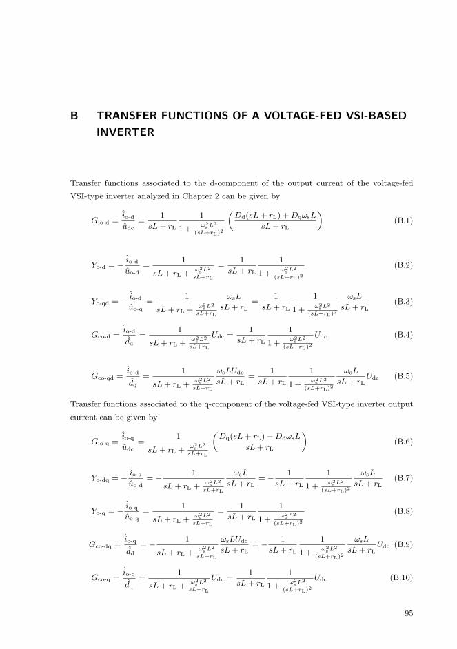
B TRANSFER FUNCTIONS OF A VOLTAGE-FED VSI-BASED
INVERTER
Transfer functions associated to the d-component of the output current of the voltage-fed
VSI-type inverter analyzed in Chapter 2 can be given by
Gio-d =io-dudc
=1
sL+ rL
1
1 +ω2s L
2
(sL+rL)2
(Dd(sL+ rL) +DqωsL
sL+ rL
)
(B.1)
Yo-d = −io-duo-d
=1
sL+ rL +ω2s L
2
sL+rL
=1
sL+ rL
1
1 +ω2s L
2
(sL+rL)2
(B.2)
Yo-qd = −io-duo-q
=1
sL+ rL +ω2sL
2
sL+rL
ωsL
sL+ rL=
1
sL+ rL
1
1 +ω2sL
2
(sL+rL)2
ωsL
sL+ rL(B.3)
Gco-d =io-d
dd=
1
sL+ rL +ω2s L
2
sL+rL
Udc =1
sL+ rL
1
1 +ω2sL
2
(sL+rL)2
Udc (B.4)
Gco-qd =io-d
dq=
1
sL+ rL +ω2s L
2
sL+rL
ωsLUdc
sL+ rL=
1
sL+ rL
1
1 +ω2s L
2
(sL+rL)2
ωsL
sL+ rLUdc (B.5)
Transfer functions associated to the q-component of the voltage-fed VSI-type inverter output
current can be given by
Gio-q =io-qudc
=1
sL+ rL +ω2sL
2
sL+rL
(Dq(sL+ rL)−DdωsL
sL+ rL
)
(B.6)
Yo-dq = −io-quo-d
= −1
sL+ rL +ω2sL
2
sL+rL
ωsL
sL+ rL= −
1
sL+ rL
1
1 +ω2s L
2
(sL+rL)2
ωsL
sL+ rL(B.7)
Yo-q = −io-quo-q
=1
sL+ rL +ω2sL
2
sL+rL
=1
sL+ rL
1
1 +ω2s L
2
(sL+rL)2
(B.8)
Gco-dq =io-q
dd= −
1
sL+ rL +ω2s L
2
sL+rL
ωsLUdc
sL+ rL= −
1
sL+ rL
1
1 +ω2s L
2
(sL+rL)2
ωsL
sL+ rLUdc (B.9)
Gco-q =io-q
dq=
1
sL+ rL +ω2s L
2
sL+rL
Udc =1
sL+ rL
1
1 +ω2sL
2
(sL+rL)2
Udc (B.10)
95

Appendix B. Transfer functions of a voltage-fed VSI-based inverter
Transfer functions associated to the input terminal of the voltage-fed VSI-type inverter can
be given by
Yin =idcudc
=1
sL+ rL +ω2s L
2
sL+rL
(3Dd
2
Dd(sL+ rL) +DqωsL
sL+ rL
+3Dq
2
Dq(sL+ rL)−DdωsL
sL+ rL
)
(B.11)
Toi-d =idcuo-d
= −1
sL+ rL
1
1 +ω2s L
2
(sL+rL)2
(3
2Dd −
3
2Dq
ωsL
sL+ rL
)
(B.12)
Toi-q =idcuo-q
= −1
sL+ rL
1
1 +ω2s L
2
(sL+rL)2
(3
2Dq +
3
2Dd
ωsL
sL+ rL
)
(B.13)
Gci-d =idc
dd=
1
sL+ rL
1
1 +ω2sL
2
(sL+rL)2
(3Dd
2Udc +
3Dq
2
ωsL
sL+ rLUdc
)
+3Io-d2
(B.14)
Gci-q =idc
dq=
1
sL+ rL
1
1 +ω2s L
2
(sL+rL)2
(3Dq
2Udc +
3Dd
2
ωsL
sL+ rLUdc
)
+3Io-q2
(B.15)
96
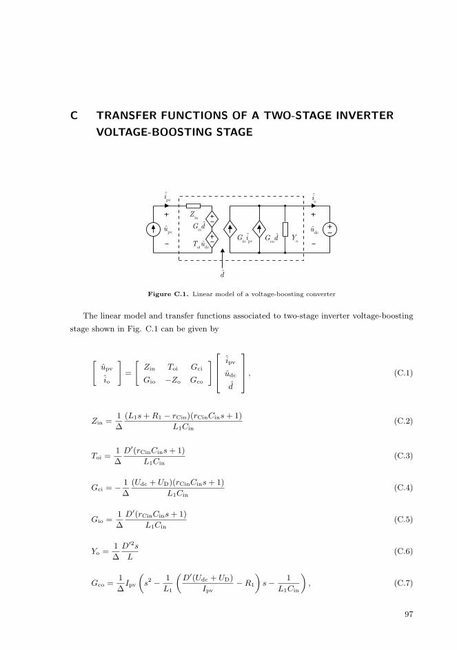
C TRANSFER FUNCTIONS OF A TWO-STAGE INVERTER
VOLTAGE-BOOSTING STAGE
oi
dcupv
u
pvi
inZ
ciˆG d
oi dcˆT u
io pvˆG i
coˆG d
oY
d
Figure C.1. Linear model of a voltage-boosting converter
The linear model and transfer functions associated to two-stage inverter voltage-boosting
stage shown in Fig. C.1 can be given by
[
upv
io
]
=
[
Zin Toi Gci
Gio −Zo Gco
]
ipv
udc
d
, (C.1)
Zin =1
∆
(L1s+R1 − rCin)(rCinCins+ 1)
L1Cin(C.2)
Toi =1
∆
D′(rCinCins+ 1)
L1Cin(C.3)
Gci = −1
∆
(Udc + UD)(rCinCins+ 1)
L1Cin(C.4)
Gio =1
∆
D′(rCinCins+ 1)
L1Cin(C.5)
Yo =1
∆
D′2s
L(C.6)
Gco =1
∆Ipv
(
s2 −1
L1
(D′(Udc + UD)
Ipv−R1
)
s−1
L1Cin
)
, (C.7)
97
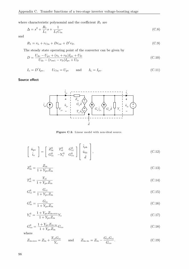
Appendix C. Transfer functions of a two-stage inverter voltage-boosting stage
where characteristic polynomial and the coefficient R1 are
∆ = s2 +R1
L1s+
1
L1Cin(C.8)
and
R1 = rL + rCin +Drsw +D′rD. (C.9)
The steady state operating point of the converter can be given by
D =Udc − Upv + (rL + rD)Ipv + UD
Udc − (rsw1 − rD)Ipv + UD(C.10)
Io = D′Ipv, UCin = Upv and IL = Ipv. (C.11)
Source effect
oi
dcupv
u
pvi
inZ
ciˆG d
oi dcˆT u
io pvˆG i
coˆG d
oY
d
phi
pvY
Figure C.2. Linear model with non-ideal source.
[
upv
io
]
=
[
ZSin T S
oi GSci
GSio −Y S
o GSco
]
iph
udc
d
, (C.12)
ZSin =
Zin
1 + YpvZin(C.13)
T Soi =
Toi
1 + YpvZin(C.14)
GSci =
Gci
1 + YpvZin(C.15)
GSio =
Gio
1 + YpvZin(C.16)
Y So =
1 + YpvZin-oco
1 + YpvZinYo (C.17)
GSco =
1 + YpvZin-∞
1 + YpvZinGco (C.18)
where
Zin-oco = Zin +ToiGio
Yoand Zin-∞ = Zin −
GioGci
Gco. (C.19)
98
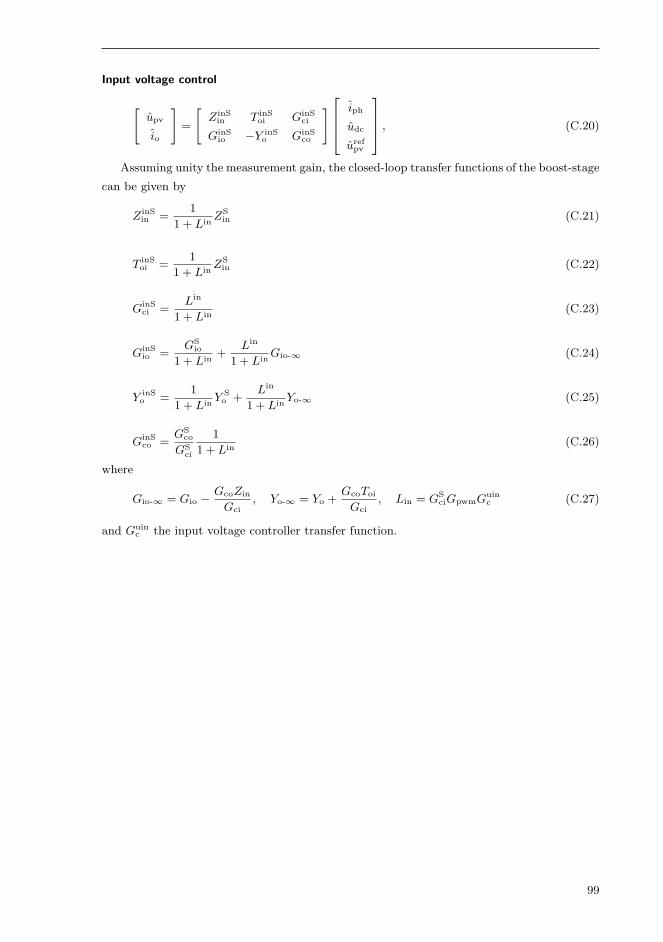
Input voltage control
[
upv
io
]
=
[
Z inSin T inS
oi GinSci
GinSio −Y inS
o GinSco
]
iph
udc
urefpv
, (C.20)
Assuming unity the measurement gain, the closed-loop transfer functions of the boost-stage
can be given by
Z inSin =
1
1 + LinZS
in (C.21)
T inSoi =
1
1 + LinZS
in (C.22)
GinSci =
Lin
1 + Lin(C.23)
GinSio =
GSio
1 + Lin+
Lin
1 + LinGio-∞ (C.24)
Y inSo =
1
1 + LinY So +
Lin
1 + LinYo-∞ (C.25)
GinSco =
GSco
GSci
1
1 + Lin(C.26)
where
Gio-∞ = Gio −GcoZin
Gci, Yo-∞ = Yo +
GcoToi
Gci, Lin = GS
ciGpwmGuinc (C.27)
and Guinc the input voltage controller transfer function.
99
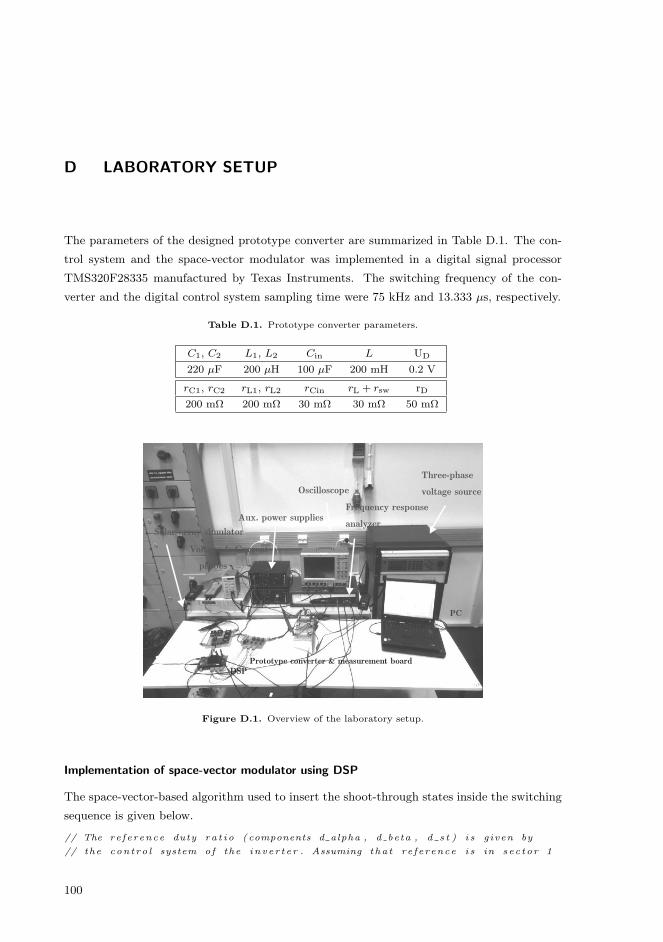
D LABORATORY SETUP
The parameters of the designed prototype converter are summarized in Table D.1. The con-
trol system and the space-vector modulator was implemented in a digital signal processor
TMS320F28335 manufactured by Texas Instruments. The switching frequency of the con-
verter and the digital control system sampling time were 75 kHz and 13.333 µs, respectively.
Table D.1. Prototype converter parameters.
C1, C2 L1, L2 Cin L UD
220 µF 200 µH 100 µF 200 mH 0.2 V
rC1, rC2 rL1, rL2 rCin rL + rsw rD
200 mΩ 200 mΩ 30 mΩ 30 mΩ 50 mΩ
Three-phase
voltage sourceOscilloscope
Aux. power supplies
Solar array simulator
Prototype converter & measurement board
DSP
PC
Frequency response
analyzer
Voltage & Current
probes
Figure D.1. Overview of the laboratory setup.
Implementation of space-vector modulator using DSP
The space-vector-based algorithm used to insert the shoot-through states inside the switching
sequence is given below.
// The re ference duty ra t i o ( components d alpha , d beta , d s t ) i s given by
// the contro l system of the inver t e r . Assuming that re ference i s in sec tor 1
100
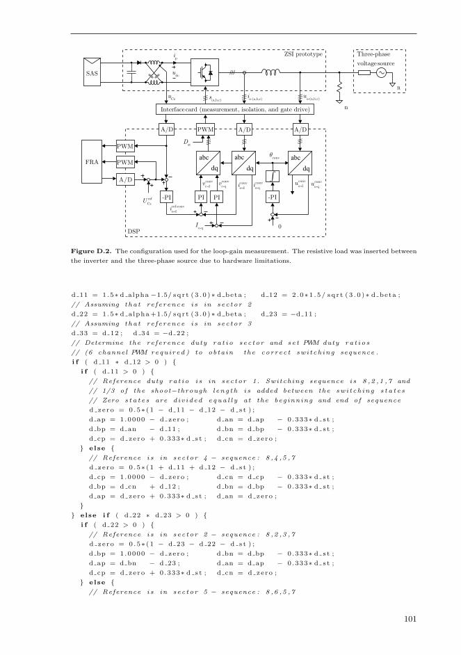
-PI
0
ò
convq
conv
o-du conv
o-qu
dq
abc
conv
o-di
conv
o-qi
conv
c-dv
conv
c-qv
PI PI
o-qI
(a,b,c)s
///
o-(a,b,c)i
///
A/D
///
///
o-(a,b,c)u
///
A/D
///
dq
abc
dq
abc
///
A/D
stD
pi
dcu
ref-conv
o-di
A/D
-PIref
CzU
Czu
PWM
n
n
PWM
PWMFRA
DSP
SAS
ZSI prototype
Interface card (measurement, isolation, and gate drive)
Three-phase
voltage source
Figure D.2. The configuration used for the loop-gain measurement. The resistive load was inserted between
the inverter and the three-phase source due to hardware limitations.
d 11 = 1.5∗ d alpha −1.5/ sq r t ( 3 . 0 )∗ d beta ; d 12 = 2 .0∗1 . 5/ sq r t ( 3 . 0 )∗ d beta ;
// Assuming that re ference i s in sec tor 2
d 22 = 1.5∗ d alpha+1.5/ sq r t ( 3 . 0 )∗ d beta ; d 23 = −d 11 ;
// Assuming that re ference i s in sec tor 3
d 33 = d 12 ; d 34 = −d 22 ;
// Determine the re ference duty ra t i o sec tor and se t PWM duty ra t i o s
// (6 channel PWM required ) to obtain the correc t swi tch ing sequence .
i f ( d 11 ∗ d 12 > 0 )
i f ( d 11 > 0 )
// Reference duty ra t i o i s in sec tor 1. Switching sequence i s 8 ,2 ,1 ,7 and
// 1/3 of the shoot−through l eng th i s added between the swi tch ing s t a t e s
// Zero s t a t e s are d iv ided equa l l y at the beginning and end of sequence
d ze ro = 0 .5∗ (1 − d 11 − d 12 − d s t ) ;
d ap = 1.0000 − d ze ro ; d an = d ap − 0.333∗ d s t ;
d bp = d an − d 11 ; d bn = d bp − 0.333∗ d s t ;
d cp = d zero + 0.333∗ d s t ; d cn = d zero ;
else
// Reference i s in sec tor 4 − sequence : 8 ,4 ,5 ,7
d ze ro = 0 .5∗ (1 + d 11 + d 12 − d s t ) ;
d cp = 1.0000 − d ze ro ; d cn = d cp − 0.333∗ d s t ;
d bp = d cn + d 12 ; d bn = d bp − 0.333∗ d s t ;
d ap = d zero + 0.333∗ d s t ; d an = d zero ;
else i f ( d 22 ∗ d 23 > 0 )
i f ( d 22 > 0 )
// Reference i s in sec tor 2 − sequence : 8 ,2 ,3 ,7
d ze ro = 0 .5∗ (1 − d 23 − d 22 − d s t ) ;
d bp = 1.0000 − d ze ro ; d bn = d bp − 0.333∗ d s t ;
d ap = d bn − d 23 ; d an = d ap − 0.333∗ d s t ;
d cp = d zero + 0.333∗ d s t ; d cn = d zero ;
else
// Reference i s in sec tor 5 − sequence : 8 ,6 ,5 ,7
101

Appendix D. Laboratory setup
d ze ro = 0 .5∗ (1 + d 23 + d 22 − d s t ) ;
d cp = 1.0000 − d ze ro ; d cn = d cp − 0.333∗ d s t ;
d ap = d cn + d 22 ; d an = d ap − 0.333∗ d s t ;
d bp = d zero + 0.333∗ d s t ; d bn = d zero ;
else i f ( d 33 > 0 )
// Reference i s in sec tor 3 − sequence : 8 ,4 ,3 ,7
d ze ro = 0 .5∗ (1 − d 34 − d 33 − d s t ) ;
d bp = 1.0000 − d ze ro ; d bn = d bp − 0.333∗ d s t ;
d cp = d bn − d 33 ; d cn = d cp − 0.333∗ d s t ;
d ap = d zero + 0.333∗ d s t ; d an = d zero ;
else
// Reference i s in sec tor 6 − sequence : 8 ,6 ,1 ,7
d ze ro = 0 .5∗ (1 + d 34 + d 33 − d s t ) ;
d ap = 1.0000 − d ze ro ; d an = d ap − 0.333∗ d s t ;
d cp = d an + d 34 ; d cn = d cp − 0.333∗ d s t ;
d bp = d zero + 0.333∗ d s t ; d bn = d zero ;
102

ISBN 978-952-15-3720-2ISSN 1459-2045
Tampereen teknillinen yliopisto PL 52733101 Tampere
Tampere University of TechnologyP.O.B. 527FI-33101 Tampere, Finland