HARMONISATION DE LANGAGES …chamilo1.grenet.fr/ujf/courses/IUT1GEIIPROSEJCINF308/document/... · 1...
113
HARMONISATION DE LANGAGES MICROPROCESSEURS • IUT1 • Département GEII • Jose-Ernesto GOMEZ-BALDERAS • [email protected]
Transcript of HARMONISATION DE LANGAGES …chamilo1.grenet.fr/ujf/courses/IUT1GEIIPROSEJCINF308/document/... · 1...

HARMONISATION DE LANGAGES
MICROPROCESSEURS
• IUT1• Département GEII• Jose-Ernesto GOMEZ-BALDERAS• [email protected]
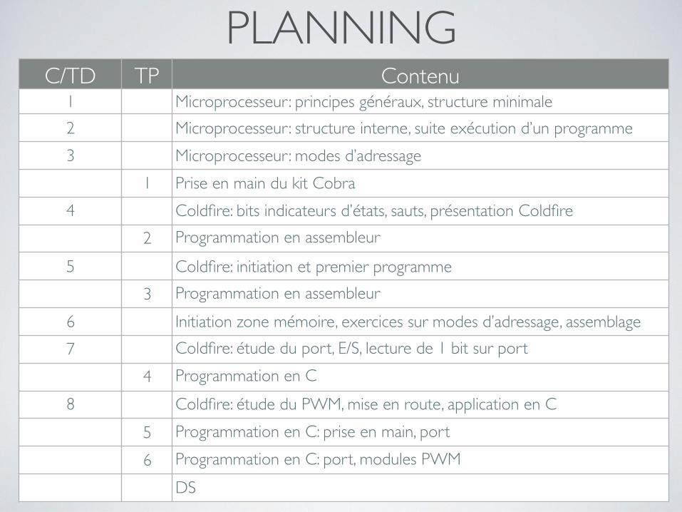
PLANNINGC/TD TP Contenu
1 Microprocesseur: principes généraux, structure minimale2 Microprocesseur: structure interne, suite exécution d’un programme3 Microprocesseur: modes d’adressage
1 Prise en main du kit Cobra4 Coldfire: bits indicateurs d’états, sauts, présentation Coldfire
2 Programmation en assembleur
5 Coldfire: initiation et premier programme3 Programmation en assembleur
6 Initiation zone mémoire, exercices sur modes d’adressage, assemblage7 Coldfire: étude du port, E/S, lecture de 1 bit sur port
4 Programmation en C8 Coldfire: étude du PWM, mise en route, application en C
5 Programmation en C: prise en main, port6 Programmation en C: port, modules PWM
DS

SOMMAIRE
1. Introduction
2. Cours
3. Architecture Von Neumman
4. Quelques aspects technologiques
5. Structure minimale
6. Structure interne

INTRODUCTION
• Informatique: science du traitement de l’information, à l’aide de machines automatiques
• Informatique industrielle: science qui recouvre l’ensemble de procédés, dans l’exploitation de processus matériels
Données d’entrée Traitement Données de sortie
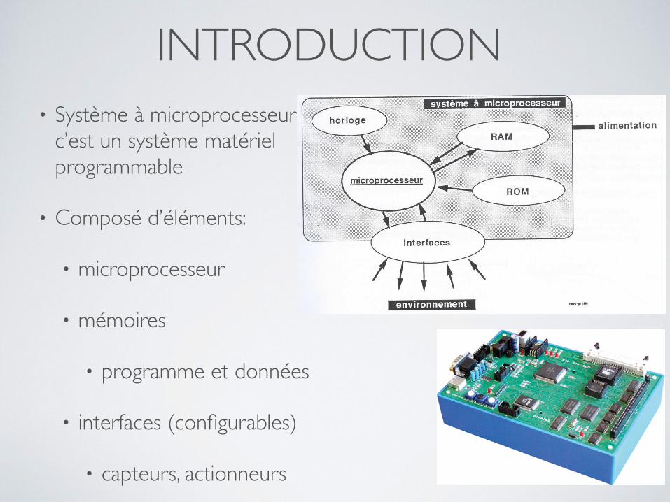
INTRODUCTION• Système à microprocesseur:
c’est un système matériel programmable
• Composé d’éléments:
• microprocesseur
• mémoires
• programme et données
• interfaces (configurables)
• capteurs, actionneurs
Figure 1. Système à microprocesseur
Microcontrôleur : le processeur travaille avec d’autres sous-ensembles de l’ordinateur
(mémoires, interfaces tels que liaison Ethernet…), les progrès de la microélectronique ont
aussi été mis à profit pour intégrer dans un seul boîtier le processeur et ces dispositifs. On
parle alors de microcontrôleur. Ce composant contient toutes les fonctions permettant la
capture des informations (interfaces d’entrée), leur traitement (processeur et mémoires) et la
production de commandes (interfaces de sortie). L’intégration de toutes ces fonctions amène
des gains appréciables en terme de coût (matériel, time to market) et de fiabilité. Elle fait
souvent choisir ce type de composant pour le contrôle de processus industriels. Le
microcontrôleur est un système à microprocesseur tout intégré.
« Microprocesseur enterré » : le ColdFire 5272 utilisé en TP présente tous les aspects d’un
microcontrôleur (très évolué) mais la majeure partie de sa mémoire est câblée en externe3. On
emploie parfois l’expression « microprocesseur enterré ».
On notera également sur la Figure 1 la présence d’une horloge. C’est elle qui rythme l’activité
du microprocesseur et à travers lui, celle du système tout entier.
3 En interne, il possède 4 ko de SRAM (c’est peu) et 1 ko de cache d’instruction. Avec les 32 bits du bus
d’adresse, on peut adresser en tout 4 Go de données ( données effectives ou instructions de programme).
IUT1 de Grenoble – Dpt GEII2 – I2 – Introduction aux systèmes d’informatique industrielle 6

INTRODUCTION
• Ordinateur: système à microprocesseur complet. Il assure la collecte d’information, son traitement, son stockage, sa restitution et sa communication
• Microprocesseur: processeur ordonnancement de tâches et leur exécution afin de traiter l’information
• Unité Centrale de Traitement UCT=CPU
1.3 / An Example System: Wading through the Jargon 5
• Pentium III 667 MHz• 133 MHz 64MB SDRAM• 32KB L1 cache, 256KB L2 cache• 30GB EIDE hard drive (7200 RPM)• 48X max variable CD-ROM• 2 USB ports, 1 serial port, 1 parallel port• 19" monitor, .24mm AG, 1280 ! 1024 at 85Hz• Intel 3D AGP graphics card• 56K PCI voice modem• 64-bit PCI sound card
FOR SALE: OBSOLETE COMPUTER – CHEAP! CHEAP! CHEAP!
FIGURE 1.1 A Typical Computer Advertisement
Kilo- (K)
Mega- (M)
Giga- (G)
Tera- (T)
Peta- (P)
(1 thousand = 103 ~ 210)
(1 million = 106 ~ 220)
(1 billion = 109 ~ 230)
(1 trillion = 1012 ~ 240)
(1 quadrillion = 1015 ~ 250)
~
~
~
~
~
Milli- (m)
Micro- (µ)
Nano- (n)
Pico- (p)
Femto- (f)
(1 thousandth = 10–3 ~ 2–10)
(1 millionth = 10–6 ~ 2–20)
(1 billionth = 10–9 ~ 2–30)
(1 trillionth = 10–12 ~ 2–40)
(1 quadrillionth = 10–15 ~ 2–50)
~
~
~
~
~
FIGURE 1.2 Common Prefixes Associated with Computer Organization andArchitecture
kilobyte (1KB) of memory is typically 1,024 bytes of memory rather than 1,000bytes of memory. However, a 1GB disk drive might actually be 1 billion bytesinstead of 230 (approximately 1.7 billion). You should always read the manufac-turer’s fine print just to make sure you know exactly what 1K, 1KB, or 1G repre-sents.
When we want to talk about how fast something is, we speak in terms of frac-tions of a second—usually thousandths, millionths, billionths, or trillionths. Pre-fixes for these metrics are given in the right-hand side of Figure 1.2. Notice thatthe fractional prefixes have exponents that are the reciprocal of the prefixes onthe left side of the figure. Therefore, if someone says to you that an operationrequires a microsecond to complete, you should also understand that a million ofthose operations could take place in one second. When you need to talk abouthow many of these things happen in a second, you would use the prefix mega-.When you need to talk about how fast the operations are performed, you woulduse the prefix micro-.
5
Principes de base Les premiers automatismes étaient réalisés à partir de la logique cablée selon le synoptique suivant :
Tableau de
commande
Automatisme à
logique câblée
Processus
Actionneurs
Capteurs
les systèmes à logique cablée sont conçus à l'aide de circuits intégrés logiques. Certains de ces circuits font appel à : La logique combinatoire
e si
i jj
(les sorties sont définis uniquement à partir des variables d'entrée)
la logique séquentielle
es
ii
jj
n
(les sorties dépendent toujours des entrées mais aussi des états antérieurs)
6
Le microprocesseur donne naissance au principe de la logique programmée. Le fonctionnement n'est plus défini par un ensemble de circuits logiques, câblés entre eux, mais par une suite ordonnée d'instructions stockées en mémoire et gérées par cet élément. Nouveau synoptique :
Tableau de
commande
Microprocesseur
Processus
Actionneurs
Capteurs
Mémoire (instructions)
Interface
Interface
Premier automatismecircuits intégrés
logique combinatoirelogique séquentielle
Nouveau synoptiqueinstructionsmémoire
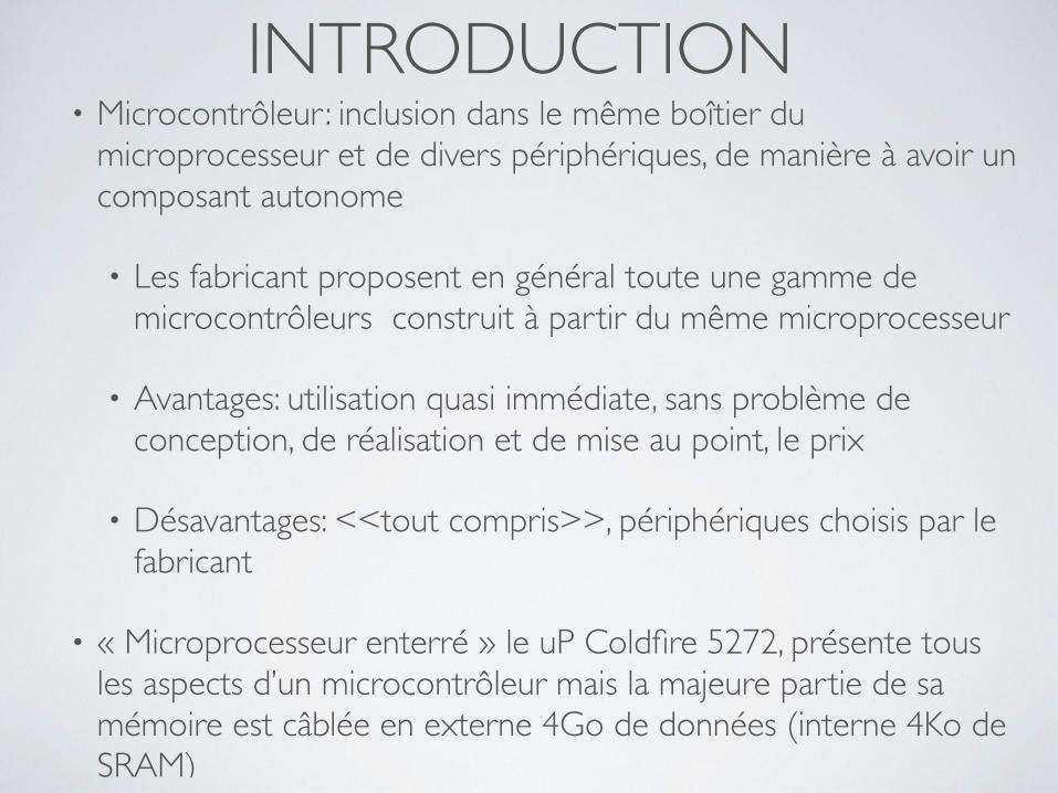
INTRODUCTION• Microcontrôleur : inclusion dans le même boîtier du
microprocesseur et de divers périphériques, de manière à avoir un composant autonome
• Les fabricant proposent en général toute une gamme de microcontrôleurs construit à partir du même microprocesseur
• Avantages: utilisation quasi immédiate, sans problème de conception, de réalisation et de mise au point, le prix
• Désavantages: <<tout compris>>, périphériques choisis par le fabricant
• « Microprocesseur enterré » le uP Coldfire 5272, présente tous les aspects d’un microcontrôleur mais la majeure partie de sa mémoire est câblée en externe 4Go de données (interne 4Ko de SRAM)

INTRODUCTION• Après le PC, les systèmes embarqués:
intègre des logiciels et des matériels conjointement et spécifiquement conçus pour assurer des fonctionnalités souvent critiques
• Dispositifs mobiles: tablettes, smartphones,.....
• Flux de données vers/du monde réel:
SYSTÈME EMBARQUÉ

SYSTÈME EMBARQUÉ
INTRODUCTIONConcernant les mémoires, celles-ci sont partagées en deux types : la RAM et la ROM. On
peut rappeler dans le Tableau 1 les acronymes liés aux différentes technologies de réalisation.
Acronyme Nom complet Comm. AcronymeNom complet
Comm.
ROM Read Only Memory RAMRandom
Access
Memory
PROMProgrammable
ROMSRAM Static RAM
Bascule RS (6
transistors)
EPROMErasable/Electrically
Programmable
ROM
DRAMDynamic
RAM
Un condensateur
et un transistor.
Rafraîchissement
EEPROMElectrically Erasable
ROMSDRAM
Synchronous
Dynamic
RAM
EEPROM flash
DDRAMDouble Data
RAM
Tableau 1. Acronymes des différents types de mémoires
IUT1 de Grenoble – Dpt GEII2 – I2 – Introduction aux systèmes d’informatique industrielle 7

INTRODUCTION1.3 Classification des microcontrôleurs et microprocesseurs
Le traitement des données par l’UCT se ramène toujours à des calculs numériques sur des
nombres binaires. Selon leur taille, on peut envisager une classification des microcontrôleurs
et des microprocesseurs comme en témoigne le Tableau 2.
Nb. bits µp, µc, DSP Exemples Usage Observations
8 µc
Pic de Microchip:
Microcontrôleurs
très simples ( le
plus petit a 6 pins)
Microcontrôleurs
classiques :
68HC11, 8051 et
dérivés
Info. indus. légère :
Photocopieur, robot
ménager,
chaudière…
Optimisés pour la
consommation et la
polyvalence plus que
la vitesse.
Très peu de calcul.
16, 32 µc, µpFamille "Coldfire"
Freescale (32 bits).
Applications plus
lourdes :
automatismes et
asservissement,
fonctions
électroniques d’un
appareil non
informatique
(autoscale d’un
oscilloscope, réveil
radio-piloté…)
Plus de calculs.
64, 128 µp
Servent à la
construction
d'ordinateurs (PC)
Optimisés pour la
vitesse et le calcul.
On n’est plus dans le
domaine de l’info.
indus. mais dans celui
de l’informatique.
32, 64DSP (Digital
Signal
Processor)
Analog Devices
Texas Instruments
Traitements son et
vidéo.
Asservissements
complexes.
Structure optimisée
pour les opérations de
filtrage et de calculs
sur les signaux audio
et vidéo.
Tableau 2. Classification des microcontrôleurs et des microprocesseurs
IUT1 de Grenoble – Dpt GEII2 – I2 – Introduction aux systèmes d’informatique industrielle 8
LE COURS
Niveau 6 Utilisateur
Niveau 5 Langage d’haut niveau
Niveau 4 Langage assembleur
Niveau 3 Software du système
Niveau 2 Langage machine
Niveau 1 Hardware
Niveau 0 Circuits intégrés
26 Chapter 1 / Introduction
Level 6
Level 5
Level 4
Level 3
Level 2
Level 1
Level 0
User
High-Level LanguageAssembly LanguageSystem SoftwareMachine
Control
Digital Logic
Executable Programs
C++, Java, FORTRAN, etc.
Assembly Code
Operating System, Library Code
Instruction Set Architecture
Microcode or Hardwired
Circuits, Gates, etc.
FIGURE 1.3 The Abstract Levels of Modern Computing Systems
well as how these layers are implemented and interface with each other. Figure 1.3shows the commonly accepted layers representing the abstract virtual machines.
Level 6, the User Level, is composed of applications and is the level withwhich everyone is most familiar. At this level, we run programs such as wordprocessors, graphics packages, or games. The lower levels are nearly invisiblefrom the User Level.
Level 5, the High-Level Language Level, consists of languages such as C,C++, FORTRAN, Lisp, Pascal, and Prolog. These languages must be translated(using either a compiler or an interpreter) to a language the machine can under-stand. Compiled languages are translated into assembly language and then assem-bled into machine code. (They are translated to the next lower level.) The user atthis level sees very little of the lower levels. Even though a programmer mustknow about data types and the instructions available for those types, she need notknow about how those types are actually implemented.
Level 4, the Assembly Language Level, encompasses some type ofassembly language. As previously mentioned, compiled higher-level lan-

ARCHITECTURE VON NEUMMANN
• John W. Mauchly et J. Presper Eckert projet secret ENIAC(WWII) DVAC (mathématicien John Von Neumman)
• Un système informatique traite des données qui peuvent être rangées en mémoire de données. Pour traiter des données, il faut qu’un programme existe. Celui-ci est rangé dans la mémoire de programme. Le tout est de ne pas les mélanger
• Programme et données sont véhiculés par le même groupe de conducteurs : le bus de données
• Pour désigner une case mémoire, le microprocesseur dépose sur le bus d’adresses du système informatique l’adresse de cette case adresse unique

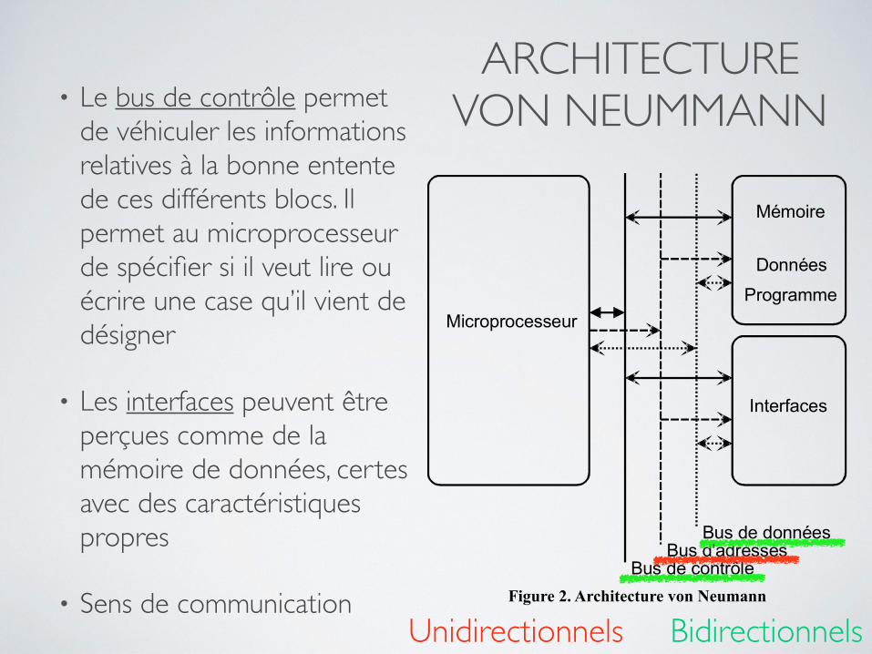
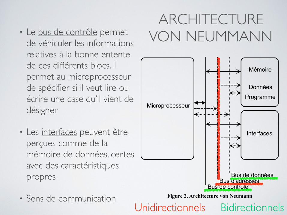
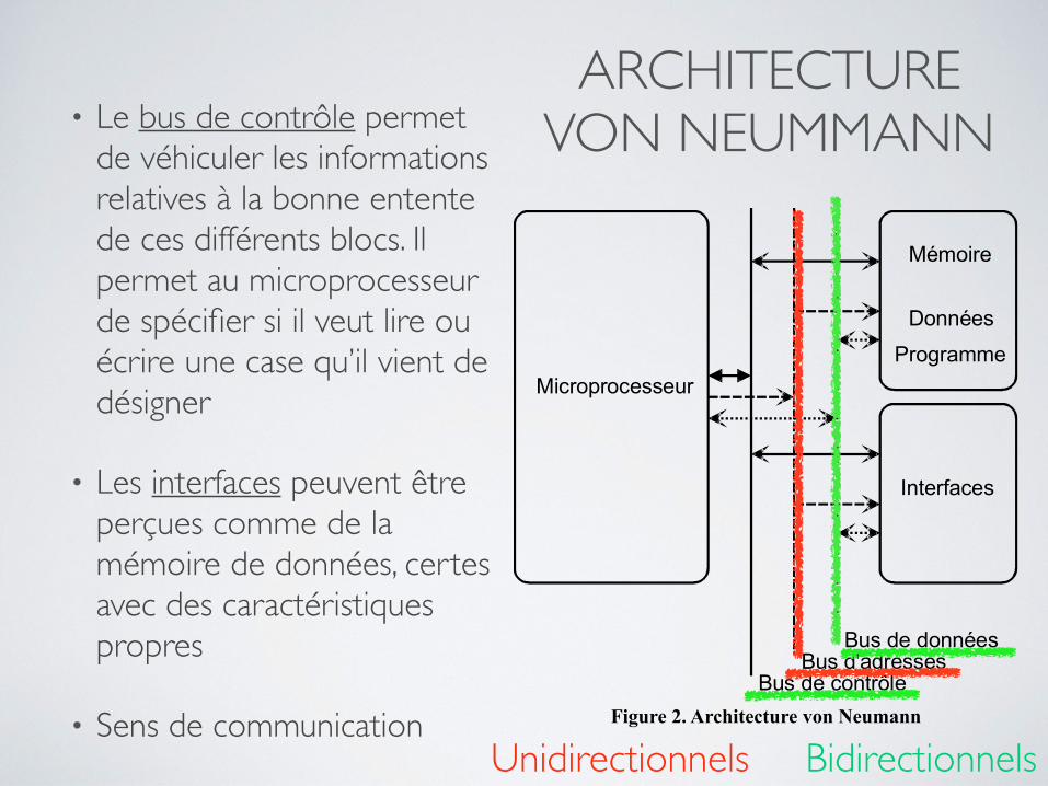
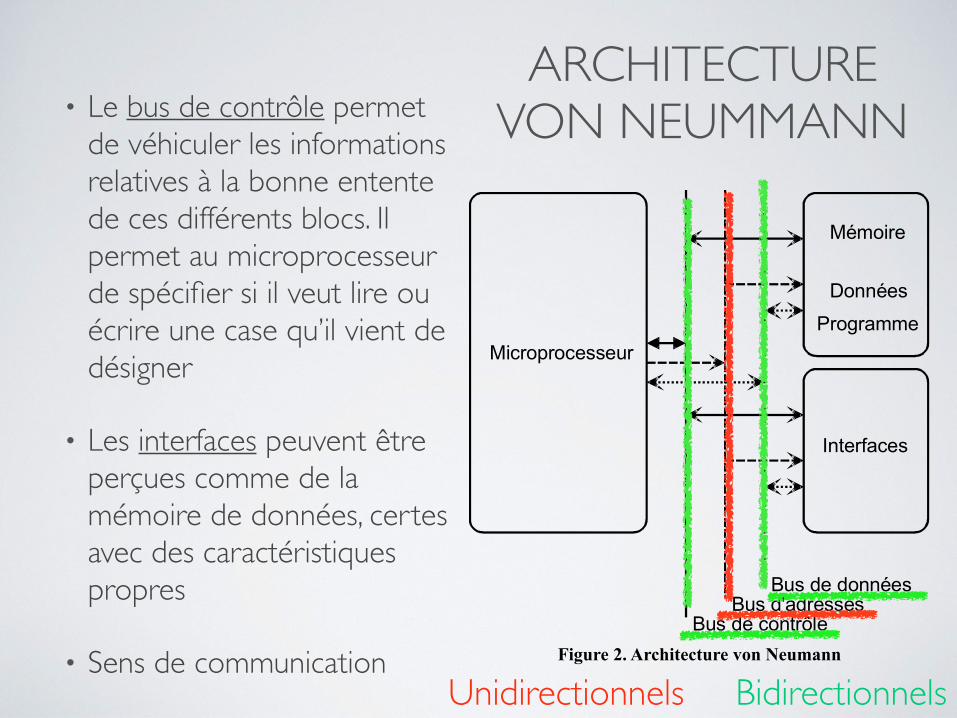
ARCHITECTURE VON NEUMMANN• Le bus de contrôle permet
de véhiculer les informations relatives à la bonne entente de ces différents blocs. Il permet au microprocesseur de spécifier si il veut lire ou écrire une case qu’il vient de désigner
• Les interfaces peuvent être perçues comme de la mémoire de données, certes avec des caractéristiques propres
• Sens de communication
Architecture von Neumann
1.4 Principe
Un système informatique traite des données qui peuvent être rangées en mémoire de données. Pour traiter des données, il faut qu’un programme existe. Celui-ci est rangé dans la
mémoire de programme.
Microprocesseur
Mémoire
Données
Programme
Interfaces
Bus de donnéesBus d'adresses
Bus de contrôle
Figure 2. Architecture von Neumann
Dans une architecture type von Neumann, dont on trouve une représentation Figure 2,
programme et données sont véhiculés par le même groupe de conducteurs : le bus de données.
Pour désigner une case mémoire, le microprocesseur dépose sur le bus d’adresses du système
informatique l’adresse de cette case.
Un même boîtier mémoire peut contenir à la fois du programme et des données, le tout est de
ne pas les mélanger. Il convient donc d’affecter à chacun des plages d’adresses différentes. La
distinction de ces deux espaces mémoire n’a pas de rapport immédiat avec la distinction
RAM/ROM.
Chaque case mémoire fait 8 bits, un octet (byte). Elle est repérée par une adresse unique.
Enfin le bus de contrôle permet de véhiculer les informations relatives à la bonne entente de
ces différents blocs. Par exemple il permet au microprocesseur de spécifier si il veut lire ou
écrire une case qu’il vient de désigner. Certains signaux du bus de contrôle peuvent aussi
servir à préciser quel boîtier mémoire parmi plusieurs est sélectionné.
IUT1 de Grenoble – Dpt GEII2 – I2 – Introduction aux systèmes d’informatique industrielle 9
Unidirectionnels Bidirectionnels
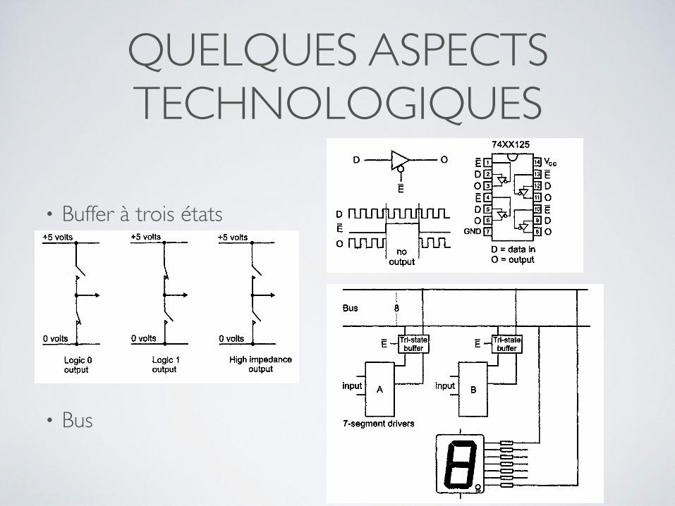
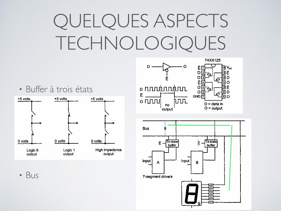
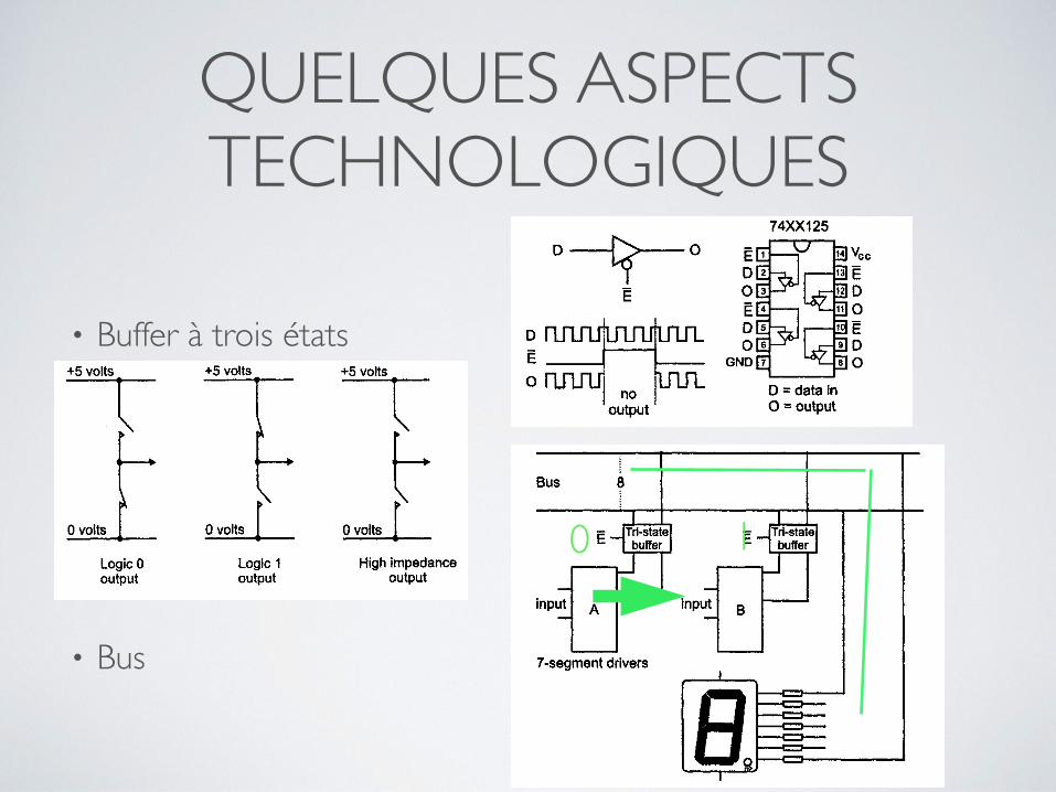
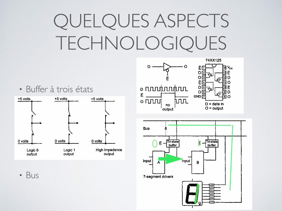
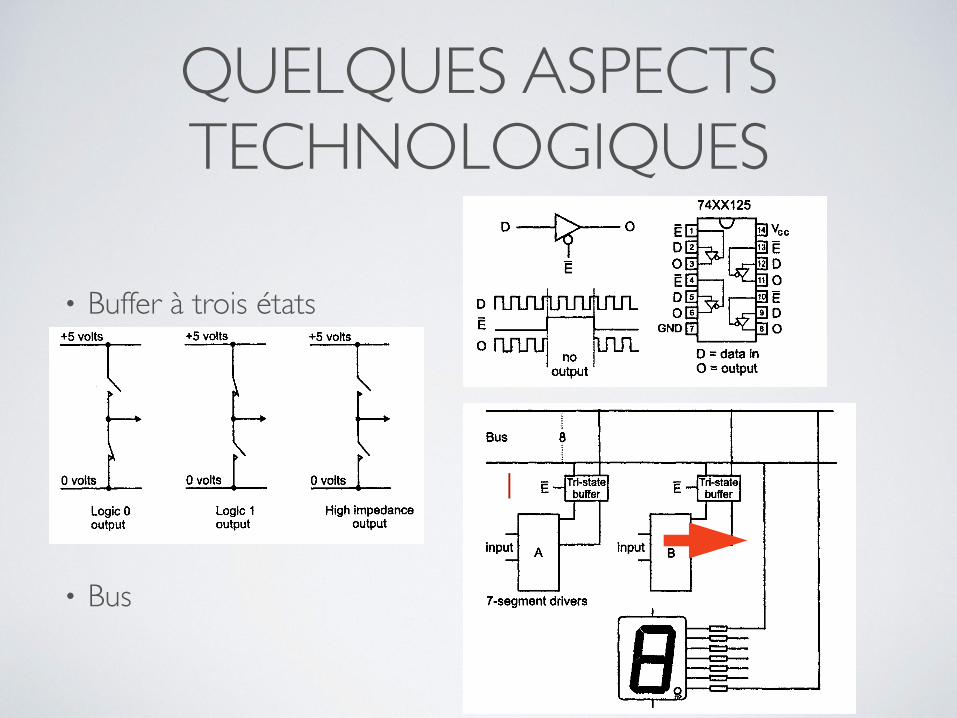
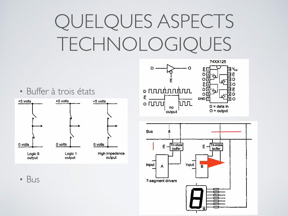
QUELQUES ASPECTS TECHNOLOGIQUES
• Buffer à trois états
• Bus
Introduction to Digital Systems 1 i i i i i i i i i i i i ii i i
'TRI-STATE' is actually a trade name owned by the National Semiconductor Corporation. Over time it has become a generic term, in the form of 'tri-state', for what should strictly be called 'three-state' devices.
To disconnect the chip there is a pin or pins called output enable (OE), or just enable (E). When these pins are held at a low logic state the chip behaves normally, providing a logic level at all the outputs that depend on the input conditions. If we take these pins high, the chip outputs are disconnected. It does this by disabling a series of tri-state buffers immediately before the data pins.
There may be several enabling pins on a chip, and not all wil l be active low though this is the most common.
Tri-state buffers A buffer is a circuit that has been added to provide isolation between two circuits, a bit like a firebreak. It reduces the chance of unwanted noise and oscillations escaping from the output back to the input and causing distortion or other mischief.
A buffer often provides voltage or current amplification, and some- times it inverts the signal. Buffers are also available in the tri-state form.
If we want to switch off a data stream, it is undesirable to use a normal on-off switch. The timing of interruption is impossible to control accurately and the switch may bounce. It is far better to use a tri-state buffer, which will connect or disconnect at the moment when the voltage is applied to the enable input.
Buffers are available in integrated form as quad, hex or octal buffers; that is, four, six or eight of them in a single chip. Figure 18.2 uses the 74XX125 quad buffer.
Figure 18.2 Switching with a tri- state buffer
2 4 4
74XX125 D ~ O D g" '~'~"J-~ Vcc
~. O D 0 ! o -
D --~ E D 0 D
o 0 no D = data in
output O = output
Transmission of digital data - - ====================== : . . . . . L [ I I I . . . . . . k . . . . . . . ILIL I I I I I l l . [ _ . i : : _ i : : : i - : i : i III . I I I l l l k l k . _ . k . . . . I I I I I . . . . . [ . . . . Z _ . : Z ~ : I : : : I : I : . Z : . . . . . . I _
Bus working Bus working is a way of reducing the number of interconnecting wires by using tri-state devices. It is very similar to the telephone system in that all our telephones use the same 'trunk' route, which acts just like a bus. The rather impractical alternative would be to have a separate wire leaving our house to each person in the world that we may wish to contact.
We are using a bus in Figure 18.3 in which the seven-segment display can be controlled by either of the two driver circuits.
Figure 18.3 On the buses
, , , , , , , , , , , , , , ,
Bus 8 , ,,, ,,,, , | . . . . . . . . . . . . . . , , , , , I "
~ ~ _.JTrl-statel
inp A [ .~_].j inp '-/buffe] I
7-segment drivers
- ' - - -4===! - " - -
If we wish to use input B to provide the signal for the display, we must isolate driver A by switching off the tri-state buffer with a high logic level on its enable input. Taking its enable input to a low state connects the buffers for input B. In this way, either of the two sets of data can use the same bus connections. For simplicity the figure shows only two circuits using the bus, but in reality there can be as many as we like providing that only one input is switched on at the same time.
On the diagram, the bus consists of only eight connections. They can all be drawn on the diagram, or we can just show the number of connections included by adding a label as in the figure. By the nature of the circuitry that is using this bus it will be a one-way route, but in other cases data can be carried in either direction as required.
A long bus often employs bus drivers that are usually tri-state buffers designed to provide high current levels. A typical example is the 74XX125.
24S
Transmission of digital data
Trl-state outputs and tri-state buffers We have seen that the output of a gate can be of a totem-pole design, with the two output transistors in series acting like a couple of switches.
Some digital circuits, particularly those using microprocessors and large scale digital circuits, have outputs with three alternative states. The output can be logic 1, logic 0 or disconnected, as in Figure 18.1. In the tri-state condition, the chip is, in effect, isolated from its output.
Figure 18.1 The three states of a tri-state
+5 volts +5 volts +5 volts
, v r
0 volts .. 0 volts _ 0 volts ..
Logic 0 Logic 1 High impedance output output output
~ 1 4 3
1
QUELQUES ASPECTS TECHNOLOGIQUES
• Buffer à trois états
• Bus
Introduction to Digital Systems 1 i i i i i i i i i i i i ii i i
'TRI-STATE' is actually a trade name owned by the National Semiconductor Corporation. Over time it has become a generic term, in the form of 'tri-state', for what should strictly be called 'three-state' devices.
To disconnect the chip there is a pin or pins called output enable (OE), or just enable (E). When these pins are held at a low logic state the chip behaves normally, providing a logic level at all the outputs that depend on the input conditions. If we take these pins high, the chip outputs are disconnected. It does this by disabling a series of tri-state buffers immediately before the data pins.
There may be several enabling pins on a chip, and not all wil l be active low though this is the most common.
Tri-state buffers A buffer is a circuit that has been added to provide isolation between two circuits, a bit like a firebreak. It reduces the chance of unwanted noise and oscillations escaping from the output back to the input and causing distortion or other mischief.
A buffer often provides voltage or current amplification, and some- times it inverts the signal. Buffers are also available in the tri-state form.
If we want to switch off a data stream, it is undesirable to use a normal on-off switch. The timing of interruption is impossible to control accurately and the switch may bounce. It is far better to use a tri-state buffer, which will connect or disconnect at the moment when the voltage is applied to the enable input.
Buffers are available in integrated form as quad, hex or octal buffers; that is, four, six or eight of them in a single chip. Figure 18.2 uses the 74XX125 quad buffer.
Figure 18.2 Switching with a tri- state buffer
2 4 4
74XX125 D ~ O D g" '~'~"J-~ Vcc
~. O D 0 ! o -
D --~ E D 0 D
o 0 no D = data in
output O = output
Transmission of digital data - - ====================== : . . . . . L [ I I I . . . . . . k . . . . . . . ILIL I I I I I l l . [ _ . i : : _ i : : : i - : i : i III . I I I l l l k l k . _ . k . . . . I I I I I . . . . . [ . . . . Z _ . : Z ~ : I : : : I : I : . Z : . . . . . . I _
Bus working Bus working is a way of reducing the number of interconnecting wires by using tri-state devices. It is very similar to the telephone system in that all our telephones use the same 'trunk' route, which acts just like a bus. The rather impractical alternative would be to have a separate wire leaving our house to each person in the world that we may wish to contact.
We are using a bus in Figure 18.3 in which the seven-segment display can be controlled by either of the two driver circuits.
Figure 18.3 On the buses
, , , , , , , , , , , , , , ,
Bus 8 , ,,, ,,,, , | . . . . . . . . . . . . . . , , , , , I "
~ ~ _.JTrl-statel
inp A [ .~_].j inp '-/buffe] I
7-segment drivers
- ' - - -4===! - " - -
If we wish to use input B to provide the signal for the display, we must isolate driver A by switching off the tri-state buffer with a high logic level on its enable input. Taking its enable input to a low state connects the buffers for input B. In this way, either of the two sets of data can use the same bus connections. For simplicity the figure shows only two circuits using the bus, but in reality there can be as many as we like providing that only one input is switched on at the same time.
On the diagram, the bus consists of only eight connections. They can all be drawn on the diagram, or we can just show the number of connections included by adding a label as in the figure. By the nature of the circuitry that is using this bus it will be a one-way route, but in other cases data can be carried in either direction as required.
A long bus often employs bus drivers that are usually tri-state buffers designed to provide high current levels. A typical example is the 74XX125.
24S
Transmission of digital data
Trl-state outputs and tri-state buffers We have seen that the output of a gate can be of a totem-pole design, with the two output transistors in series acting like a couple of switches.
Some digital circuits, particularly those using microprocessors and large scale digital circuits, have outputs with three alternative states. The output can be logic 1, logic 0 or disconnected, as in Figure 18.1. In the tri-state condition, the chip is, in effect, isolated from its output.
Figure 18.1 The three states of a tri-state
+5 volts +5 volts +5 volts
, v r
0 volts .. 0 volts _ 0 volts ..
Logic 0 Logic 1 High impedance output output output
~ 1 4 3
10

QUELQUES ASPECTS TECHNOLOGIQUES
• Buffer à trois états
• Bus
Introduction to Digital Systems 1 i i i i i i i i i i i i ii i i
'TRI-STATE' is actually a trade name owned by the National Semiconductor Corporation. Over time it has become a generic term, in the form of 'tri-state', for what should strictly be called 'three-state' devices.
To disconnect the chip there is a pin or pins called output enable (OE), or just enable (E). When these pins are held at a low logic state the chip behaves normally, providing a logic level at all the outputs that depend on the input conditions. If we take these pins high, the chip outputs are disconnected. It does this by disabling a series of tri-state buffers immediately before the data pins.
There may be several enabling pins on a chip, and not all wil l be active low though this is the most common.
Tri-state buffers A buffer is a circuit that has been added to provide isolation between two circuits, a bit like a firebreak. It reduces the chance of unwanted noise and oscillations escaping from the output back to the input and causing distortion or other mischief.
A buffer often provides voltage or current amplification, and some- times it inverts the signal. Buffers are also available in the tri-state form.
If we want to switch off a data stream, it is undesirable to use a normal on-off switch. The timing of interruption is impossible to control accurately and the switch may bounce. It is far better to use a tri-state buffer, which will connect or disconnect at the moment when the voltage is applied to the enable input.
Buffers are available in integrated form as quad, hex or octal buffers; that is, four, six or eight of them in a single chip. Figure 18.2 uses the 74XX125 quad buffer.
Figure 18.2 Switching with a tri- state buffer
2 4 4
74XX125 D ~ O D g" '~'~"J-~ Vcc
~. O D 0 ! o -
D --~ E D 0 D
o 0 no D = data in
output O = output
Transmission of digital data - - ====================== : . . . . . L [ I I I . . . . . . k . . . . . . . ILIL I I I I I l l . [ _ . i : : _ i : : : i - : i : i III . I I I l l l k l k . _ . k . . . . I I I I I . . . . . [ . . . . Z _ . : Z ~ : I : : : I : I : . Z : . . . . . . I _
Bus working Bus working is a way of reducing the number of interconnecting wires by using tri-state devices. It is very similar to the telephone system in that all our telephones use the same 'trunk' route, which acts just like a bus. The rather impractical alternative would be to have a separate wire leaving our house to each person in the world that we may wish to contact.
We are using a bus in Figure 18.3 in which the seven-segment display can be controlled by either of the two driver circuits.
Figure 18.3 On the buses
, , , , , , , , , , , , , , ,
Bus 8 , ,,, ,,,, , | . . . . . . . . . . . . . . , , , , , I "
~ ~ _.JTrl-statel
inp A [ .~_].j inp '-/buffe] I
7-segment drivers
- ' - - -4===! - " - -
If we wish to use input B to provide the signal for the display, we must isolate driver A by switching off the tri-state buffer with a high logic level on its enable input. Taking its enable input to a low state connects the buffers for input B. In this way, either of the two sets of data can use the same bus connections. For simplicity the figure shows only two circuits using the bus, but in reality there can be as many as we like providing that only one input is switched on at the same time.
On the diagram, the bus consists of only eight connections. They can all be drawn on the diagram, or we can just show the number of connections included by adding a label as in the figure. By the nature of the circuitry that is using this bus it will be a one-way route, but in other cases data can be carried in either direction as required.
A long bus often employs bus drivers that are usually tri-state buffers designed to provide high current levels. A typical example is the 74XX125.
24S
Transmission of digital data
Trl-state outputs and tri-state buffers We have seen that the output of a gate can be of a totem-pole design, with the two output transistors in series acting like a couple of switches.
Some digital circuits, particularly those using microprocessors and large scale digital circuits, have outputs with three alternative states. The output can be logic 1, logic 0 or disconnected, as in Figure 18.1. In the tri-state condition, the chip is, in effect, isolated from its output.
Figure 18.1 The three states of a tri-state
+5 volts +5 volts +5 volts
, v r
0 volts .. 0 volts _ 0 volts ..
Logic 0 Logic 1 High impedance output output output
~ 1 4 3
1
QUELQUES ASPECTS TECHNOLOGIQUES
• Buffer à trois états
• Bus
Introduction to Digital Systems 1 i i i i i i i i i i i i ii i i
'TRI-STATE' is actually a trade name owned by the National Semiconductor Corporation. Over time it has become a generic term, in the form of 'tri-state', for what should strictly be called 'three-state' devices.
To disconnect the chip there is a pin or pins called output enable (OE), or just enable (E). When these pins are held at a low logic state the chip behaves normally, providing a logic level at all the outputs that depend on the input conditions. If we take these pins high, the chip outputs are disconnected. It does this by disabling a series of tri-state buffers immediately before the data pins.
There may be several enabling pins on a chip, and not all wil l be active low though this is the most common.
Tri-state buffers A buffer is a circuit that has been added to provide isolation between two circuits, a bit like a firebreak. It reduces the chance of unwanted noise and oscillations escaping from the output back to the input and causing distortion or other mischief.
A buffer often provides voltage or current amplification, and some- times it inverts the signal. Buffers are also available in the tri-state form.
If we want to switch off a data stream, it is undesirable to use a normal on-off switch. The timing of interruption is impossible to control accurately and the switch may bounce. It is far better to use a tri-state buffer, which will connect or disconnect at the moment when the voltage is applied to the enable input.
Buffers are available in integrated form as quad, hex or octal buffers; that is, four, six or eight of them in a single chip. Figure 18.2 uses the 74XX125 quad buffer.
Figure 18.2 Switching with a tri- state buffer
2 4 4
74XX125 D ~ O D g" '~'~"J-~ Vcc
~. O D 0 ! o -
D --~ E D 0 D
o 0 no D = data in
output O = output
Transmission of digital data - - ====================== : . . . . . L [ I I I . . . . . . k . . . . . . . ILIL I I I I I l l . [ _ . i : : _ i : : : i - : i : i III . I I I l l l k l k . _ . k . . . . I I I I I . . . . . [ . . . . Z _ . : Z ~ : I : : : I : I : . Z : . . . . . . I _
Bus working Bus working is a way of reducing the number of interconnecting wires by using tri-state devices. It is very similar to the telephone system in that all our telephones use the same 'trunk' route, which acts just like a bus. The rather impractical alternative would be to have a separate wire leaving our house to each person in the world that we may wish to contact.
We are using a bus in Figure 18.3 in which the seven-segment display can be controlled by either of the two driver circuits.
Figure 18.3 On the buses
, , , , , , , , , , , , , , ,
Bus 8 , ,,, ,,,, , | . . . . . . . . . . . . . . , , , , , I "
~ ~ _.JTrl-statel
inp A [ .~_].j inp '-/buffe] I
7-segment drivers
- ' - - -4===! - " - -
If we wish to use input B to provide the signal for the display, we must isolate driver A by switching off the tri-state buffer with a high logic level on its enable input. Taking its enable input to a low state connects the buffers for input B. In this way, either of the two sets of data can use the same bus connections. For simplicity the figure shows only two circuits using the bus, but in reality there can be as many as we like providing that only one input is switched on at the same time.
On the diagram, the bus consists of only eight connections. They can all be drawn on the diagram, or we can just show the number of connections included by adding a label as in the figure. By the nature of the circuitry that is using this bus it will be a one-way route, but in other cases data can be carried in either direction as required.
A long bus often employs bus drivers that are usually tri-state buffers designed to provide high current levels. A typical example is the 74XX125.
24S
Transmission of digital data
Trl-state outputs and tri-state buffers We have seen that the output of a gate can be of a totem-pole design, with the two output transistors in series acting like a couple of switches.
Some digital circuits, particularly those using microprocessors and large scale digital circuits, have outputs with three alternative states. The output can be logic 1, logic 0 or disconnected, as in Figure 18.1. In the tri-state condition, the chip is, in effect, isolated from its output.
Figure 18.1 The three states of a tri-state
+5 volts +5 volts +5 volts
, v r
0 volts .. 0 volts _ 0 volts ..
Logic 0 Logic 1 High impedance output output output
~ 1 4 3
1

QUELQUES ASPECTS TECHNOLOGIQUES
• Buffer à trois états
• Bus
Introduction to Digital Systems 1 i i i i i i i i i i i i ii i i
'TRI-STATE' is actually a trade name owned by the National Semiconductor Corporation. Over time it has become a generic term, in the form of 'tri-state', for what should strictly be called 'three-state' devices.
To disconnect the chip there is a pin or pins called output enable (OE), or just enable (E). When these pins are held at a low logic state the chip behaves normally, providing a logic level at all the outputs that depend on the input conditions. If we take these pins high, the chip outputs are disconnected. It does this by disabling a series of tri-state buffers immediately before the data pins.
There may be several enabling pins on a chip, and not all wil l be active low though this is the most common.
Tri-state buffers A buffer is a circuit that has been added to provide isolation between two circuits, a bit like a firebreak. It reduces the chance of unwanted noise and oscillations escaping from the output back to the input and causing distortion or other mischief.
A buffer often provides voltage or current amplification, and some- times it inverts the signal. Buffers are also available in the tri-state form.
If we want to switch off a data stream, it is undesirable to use a normal on-off switch. The timing of interruption is impossible to control accurately and the switch may bounce. It is far better to use a tri-state buffer, which will connect or disconnect at the moment when the voltage is applied to the enable input.
Buffers are available in integrated form as quad, hex or octal buffers; that is, four, six or eight of them in a single chip. Figure 18.2 uses the 74XX125 quad buffer.
Figure 18.2 Switching with a tri- state buffer
2 4 4
74XX125 D ~ O D g" '~'~"J-~ Vcc
~. O D 0 ! o -
D --~ E D 0 D
o 0 no D = data in
output O = output
Transmission of digital data - - ====================== : . . . . . L [ I I I . . . . . . k . . . . . . . ILIL I I I I I l l . [ _ . i : : _ i : : : i - : i : i III . I I I l l l k l k . _ . k . . . . I I I I I . . . . . [ . . . . Z _ . : Z ~ : I : : : I : I : . Z : . . . . . . I _
Bus working Bus working is a way of reducing the number of interconnecting wires by using tri-state devices. It is very similar to the telephone system in that all our telephones use the same 'trunk' route, which acts just like a bus. The rather impractical alternative would be to have a separate wire leaving our house to each person in the world that we may wish to contact.
We are using a bus in Figure 18.3 in which the seven-segment display can be controlled by either of the two driver circuits.
Figure 18.3 On the buses
, , , , , , , , , , , , , , ,
Bus 8 , ,,, ,,,, , | . . . . . . . . . . . . . . , , , , , I "
~ ~ _.JTrl-statel
inp A [ .~_].j inp '-/buffe] I
7-segment drivers
- ' - - -4===! - " - -
If we wish to use input B to provide the signal for the display, we must isolate driver A by switching off the tri-state buffer with a high logic level on its enable input. Taking its enable input to a low state connects the buffers for input B. In this way, either of the two sets of data can use the same bus connections. For simplicity the figure shows only two circuits using the bus, but in reality there can be as many as we like providing that only one input is switched on at the same time.
On the diagram, the bus consists of only eight connections. They can all be drawn on the diagram, or we can just show the number of connections included by adding a label as in the figure. By the nature of the circuitry that is using this bus it will be a one-way route, but in other cases data can be carried in either direction as required.
A long bus often employs bus drivers that are usually tri-state buffers designed to provide high current levels. A typical example is the 74XX125.
24S
Transmission of digital data
Trl-state outputs and tri-state buffers We have seen that the output of a gate can be of a totem-pole design, with the two output transistors in series acting like a couple of switches.
Some digital circuits, particularly those using microprocessors and large scale digital circuits, have outputs with three alternative states. The output can be logic 1, logic 0 or disconnected, as in Figure 18.1. In the tri-state condition, the chip is, in effect, isolated from its output.
Figure 18.1 The three states of a tri-state
+5 volts +5 volts +5 volts
, v r
0 volts .. 0 volts _ 0 volts ..
Logic 0 Logic 1 High impedance output output output
~ 1 4 3
1 0
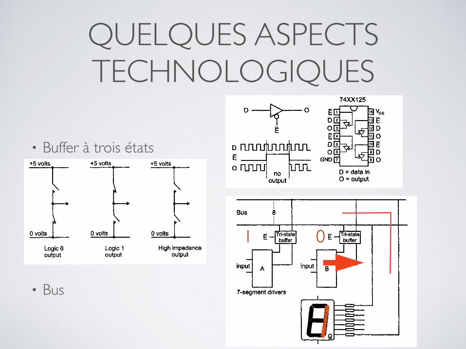
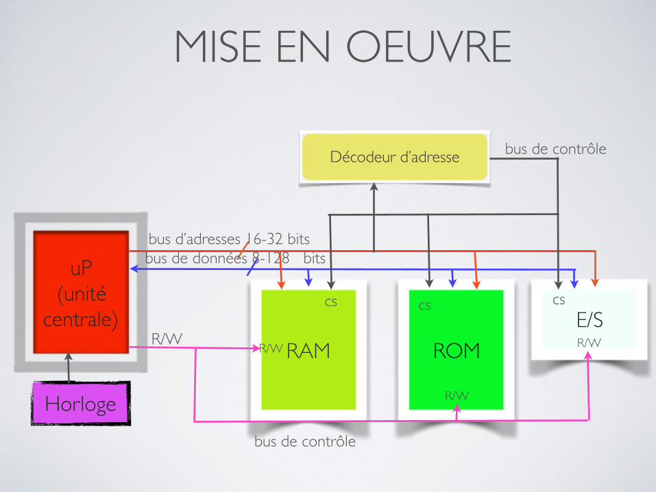
MISE EN OEUVRE
uP(unité
centrale)
Horloge
RAM ROME/S
Décodeur d’adresse
cscs cs
R/W
R/W
R/W
bus d’adresses 16-32 bits bus de données 8-128 bits
R/W
bus de contrôle
bus de contrôle
ARCHITECTURE MCF5272
1. Présentation du Coldfire MCF5272
Le Motorola ColdFire 5272 est un microcontrôleur RISC1 32 bits. En tant que microcontrôleur, il intègre donc une unité centrale (qu'on appellera aussi cœur ou core), de la RAM, et de nombreux périphériques d'entrées/sorties permettant d'envisager un très grand nombre de modes de communication avec son environnement. En revanche, contrairement au 5282, il ne possède pas de ROM (EEPROM Flash) et ne peut donc pas fonctionner en "stand alone". Il sera donc nécessairement accompagné par une EEPROM et éventuellement par de la RAM.
Le cœur ("core" - noyau - en anglais) est hérité de l'architecture de la famille 68000 de Motorola, conçue à la fin des années 70. Son unité arithmétique et logique et ses registres de manipulation des données et des adresses sont d'une taille de 32 bits.
La famille Coldfire se décompose en trois catégories de cœurs (V2, V3, V4(e)). Le MCF5272 a un cœur V2. Pour chaque type de cœur existe une grande variété de composants comprenant un nombre important de modules périphériques. Le choix du composant pour une application industrielle donnée est donc en grande partie guidé par les modules périphériques intégrés au circuit.
2. Architecture périphérique du MCF5272
3. Lecture – écriture des registres des modules périphériques
3.1. Généralités
Dans un Colfire, (à l'inverse des systèmes à base d'Intel x86), les registres des modules périphériques sont considérés comme des cases mémoires. Ils sont donc dans le même plan mémoire que la RAM et la ROM et occupent une place qui ne doit pas se chevaucher avec la RAM ou la ROM. Le Coldfire possède un décodeur d'adresses interne au composant, qui génère des signaux de "chip select" pour sélectionner la RAM, la ROM, les
1 RISC - Reduced Instruction Set Computer : processeur à jeu d'instruction réduit. Ce type de processeur exécute normalement une instruction par cycle d'horloge. Sur le MCF5272 cadencé à 66 Mhz, chaque instruction est exécutée en 60 ns sauf quelques unes qui ne respectent pas cette règle (exemple : division)
IUT1 – Dpt GEII2 - Informatique Industrielle : Coldfire-Périphériques Page 5/24
Coeur V2 Timers 0, 1, 2, 3
UARTs 0, 1
PWMs 0, 1, 2Ethernet
USB QSPI
PLIC (RNIS)
Ports A, B, C
Extension bus d'adresse
Extension bus de données
Bus d'adresses externe 23 bits
Bus de données externe 16/32 bits
63 broches configurables pour les E/S des modules périphériques
Bus d'adresses interne 32 bitsBus de données interne 32 bits
Modules périphériques
Unité centrale
SRAM4 ko
Cache1 ko
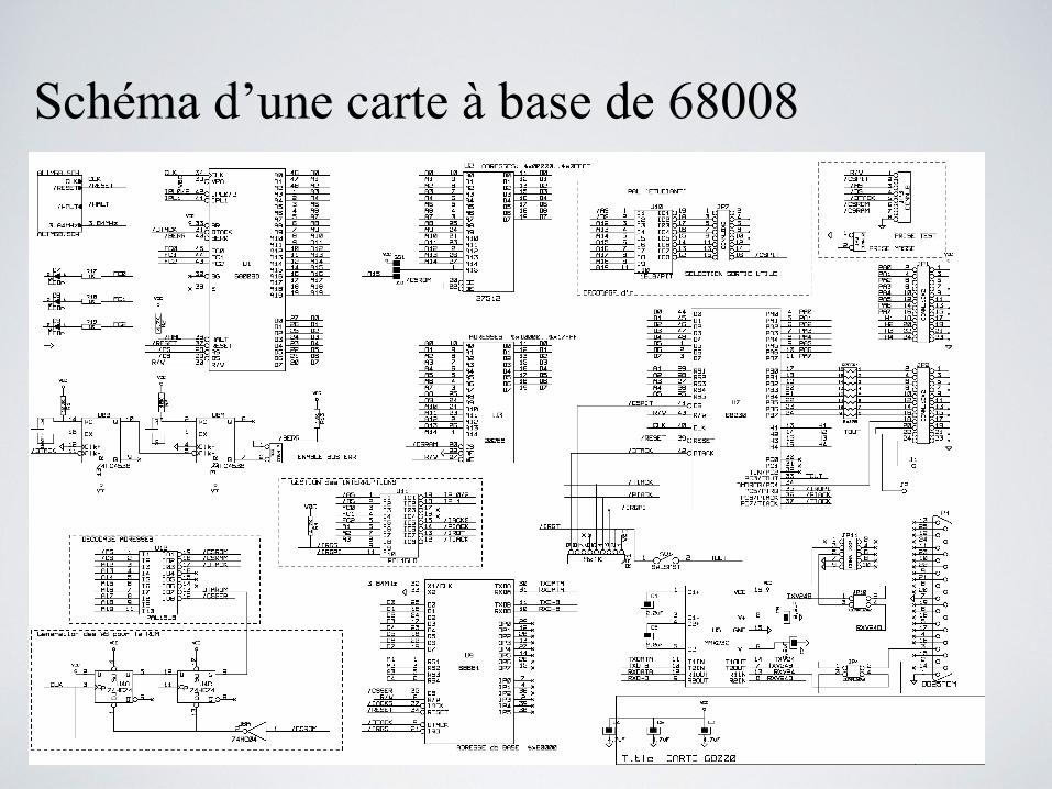
Schéma d’une carte à base de 68008
Fig
ure
4. C
arte
à b
ase
de
6800
8
IUT
1 d
e G
renoble
– D
pt G
EII2 –
I2 –
Intr
oduction a
ux s
ystè
mes d
’info
rmatique industr
ielle
12
LA NOTION DE PROGRAMME• Un programme qui réalise une fonction particulière comprend:
• une suite d’instructions (action élémentaire)
• instruction est constituée de plusieurs micro-instructions
• micro-instruction génère plusieurs micro-commandes (mots dans une mémoire)
• Jeu d’instructions (Coldfire MCF5272 != PIC16FXX)
• Instruction code binaire = op. code, 16, 32, 48 bits (1 mots = 16bits)
UNITÉ DE COMMANDE• (control unit) comprend 3 éléments:
• Le compteur ordinal (PC), registre 32 bits qui contient l’adresse de l’emplacement de la mémoire de programme. Il faut aller chercher (fetch) l’op. code de la prochaine instruction
• L’op. code est rangé à l’intérieur du microprocesseur dans le registre d’instruction
• Le décodeur d’instruction-séquenceur
1. décode l’op. code, en fonction du résultat
2. génère à diverses instants successifs les commandes spécifiques assurant l’exécution de l’instruction
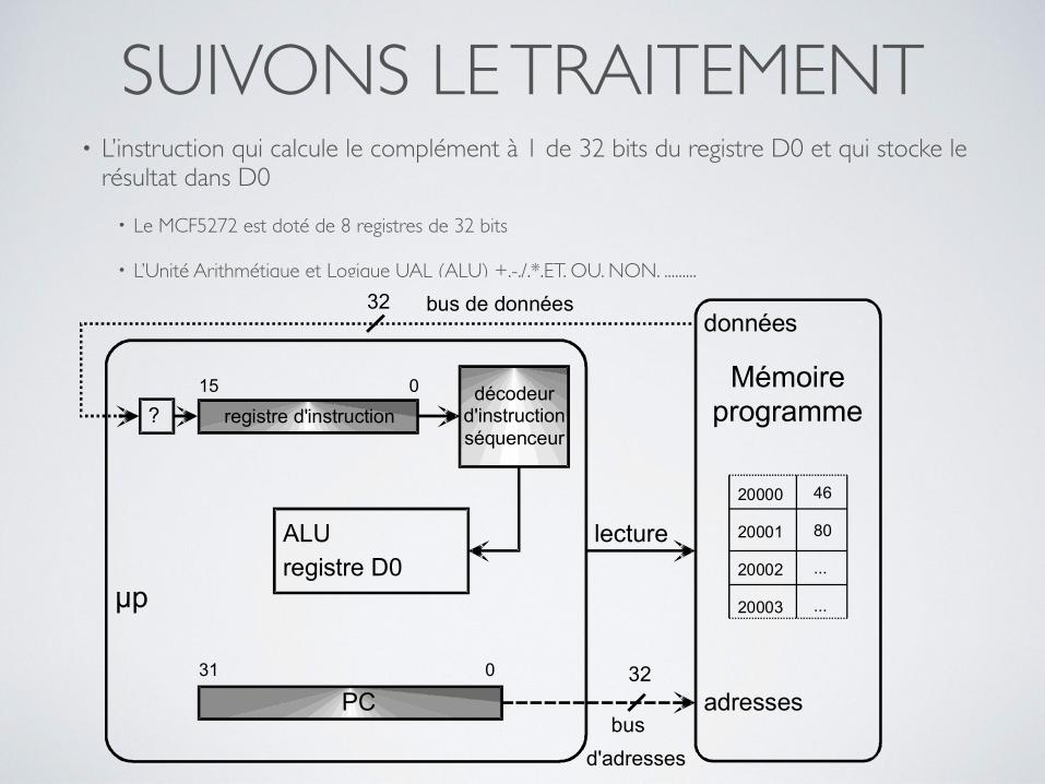
SUIVONS LE TRAITEMENT• L’instruction qui calcule le complément à 1 de 32 bits du registre D0 et qui stocke le
résultat dans D0• Le MCF5272 est doté de 8 registres de 32 bits
• L’Unité Arithmétique et Logique UAL (ALU) +,-,/,*,ET, OU, NON, .........
Pour cela, nous avons besoin de présenter succinctement deux éléments du microprocesseur
qui permettent ce calcul (on trouvera plus de détails dans la partie 1.9) :
• Le MCF5272 est doté de 8 registres de données de 32 bits nommés D0 à D7 servant
pour le calcul. Ils sont associés à l’ALU (cf. ci-dessous) via un bus de données interne
au microprocesseur.
• L’Unité Arithmétique et Logique (Arithmetic and Logic Unit - ALU) est un sous
ensemble du microprocesseur chargé des calculs arithmétiques (+, -, x, /) et logiques
(ET, OU, OU exclusif et NON qui est l’opération qui nous intéresse ici). Elle admet en
entrée des opérandes (en général un ou deux, selon l’opération) stockés dans les
registres (ou la mémoire) et produit en sortie un résultat qu’elle stocke dans un registre
(ou la mémoire). Grâce au bus de données interne du microprocesseur, ALU et
registres communiquent très rapidement, plus qu’entre ALU et mémoire externe par
exemple.
Les différents éléments présentés jusqu’à maintenant se retrouvent sur la Figure 5 où l’on
pourra suivre le traitement de l’instruction présentée.
Pour complémenter les 32 bits du registre D0 et stocker le résultat dans D0, le programmeur a
stocké dans la mémoire de programme l’op. code 46806. Supposons qu’il ait stocké cet op.
code aux adresses 20000 et 20001.
015
lecture
32
PC
bus de données
bus
d'adresses
ALU
registre D0
Mémoireprogramme
données
adresses
031
20000
20001
20002
20003
46
80
...
...
registre d'instruction
décodeurd'instructionséquenceur
µp
32
?
Figure 5. Le traitement des instructions grâce à l’unité de commande (en grisé)
Suivons Figure 5 ce qu’il se passe :
1. Le PC dépose son contenu, 20000, sur le bus d’adresses.
2. Une lecture est commandée (lecture = 1). Le contenu des cases mémoire 20000 et 20001,
4680, est transféré (sauvegardé) dans le registre d’instruction via le bus de données, qui va
du coup pouvoir servir à autre chose. La phase de fetch est terminée.
6 On travaille en hexadécimal dans ce document. 4680 est donc une instruction sur 16 bits. Les cases mémoire
faisant 8 bits (un octet), il en faut deux pour loger une instruction 16 bits. Comme on l’a déjà signalé, il existe
aussi des instructions codées sur 32 bits (4 octets) et d’autres sur 48 bits (6 octets).
IUT1 de Grenoble – Dpt GEII2 – I2 – Introduction aux systèmes d’informatique industrielle 14
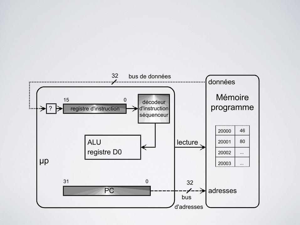
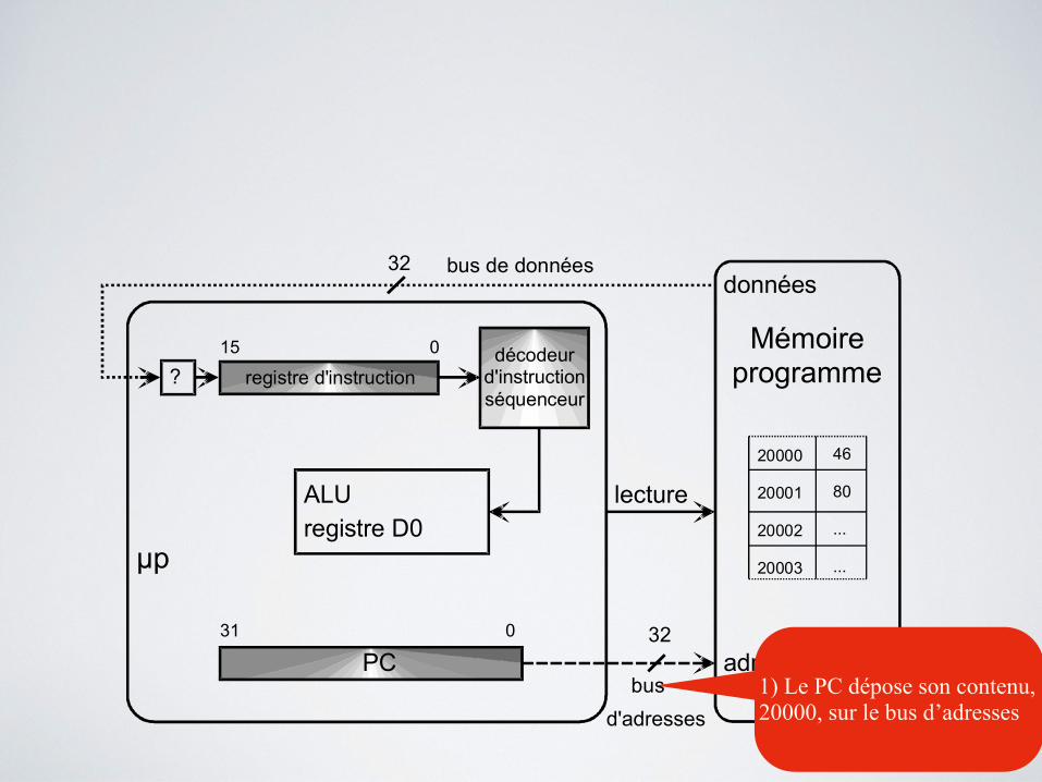
1) Le PC dépose son contenu, 20000, sur le bus d’adresses
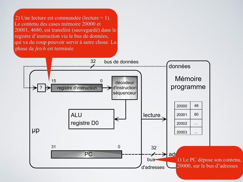
2) Une lecture est commandée (lecture = 1). Le contenu des cases mémoire 20000 et 20001, 4680, est transféré (sauvegardé) dans le registre d’instruction via le bus de données, qui va du coup pouvoir servir à autre chose. La phase de fetch est terminée
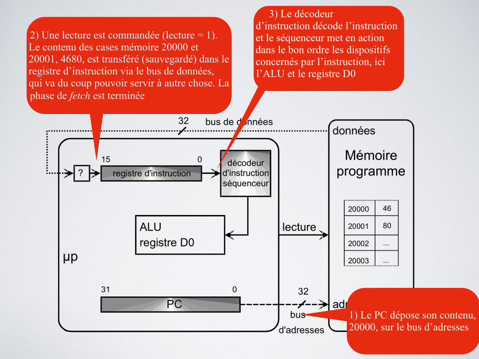
3) Le décodeur d’instruction décode l’instruction et le séquenceur met en action dans le bon ordre les dispositifs concernés par l’instruction, ici l’ALU et le registre D0
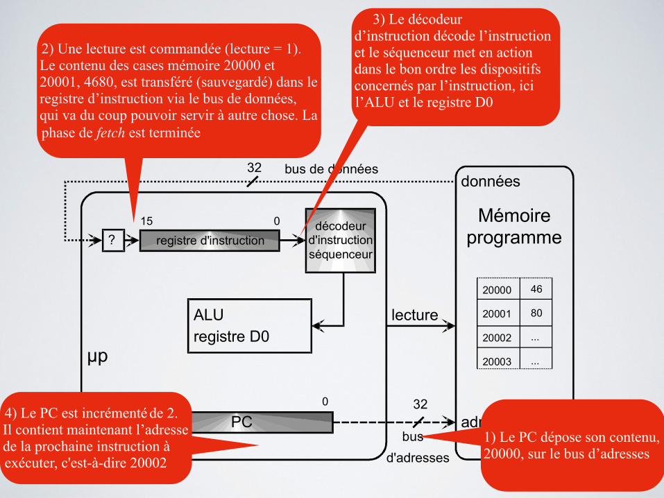
4) Le PC est incrémenté de 2. Il contient maintenant l’adresse de la prochaine instruction à exécuter, c'est-à-dire 20002
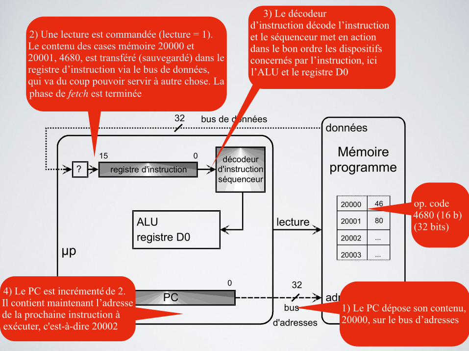
op. code 4680 (16 b)(32 bits)
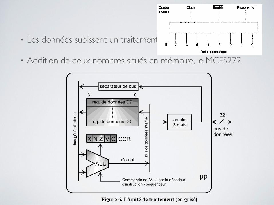
• Les données subissent un traitement
• Addition de deux nombres situés en mémoire, le MCF5272
L’unité de traitement
1.9 Constitution de l’unité de traitement
Les données, échangées par le microprocesseur avec les autres circuits (mémoires et
interfaces), subissent un traitement à l’intérieur du microprocesseur. Par exemple, on peut
envisager l’addition de deux nombres situés en mémoire. Pour cela, le MCF5272 possède 4
éléments8 que l’on peut regrouper dans un bloc fonctionnel nommé unité de traitement (Figure 6) :
• 8 registres de données de 32 bits nommés D0 à D7 ;
• une Unité Arithmétique et Logique (Arithmetic and Logic Unit - ALU) dont le
fonctionnement a été introduit dans la partie 1.8 ;
• un registre CCR (Condition Code Register). Associé à l’ALU, il rend compte du
dernier calcul effectué : génération de retenue, dépassement de capacité… ;
• une unité de multiplication-accumulation spécialement conçue pour le traitement du
signal mais dont nous ne parlerons pas dans ce cours9.
ALU
X N CZ V CCR
amplis3 états
Commande de l'ALU par le décodeurd'instruction - séquenceur
bu
s d
e d
onné
es inte
rne
031
résultat
µp
séparateur de bus
bu
s g
éné
ral in
tern
e
bus dedonnées
32
reg. de données D0
reg. de données D7
Figure 6. L'unité de traitement (en grisé)
8 Le MCF5272 ne possède pas d’unité de virgule flottante (Floating Point Unit - FPU) mais d’autres
microprocesseurs de la famille MCF en sont dotés. La représentation en virgule flottante permet de
représenter des nombres non entiers ayant des ordres de grandeurs très différents. Quand le microprocesseur ne
possède pas de FPU, la représentation des nombres non entiers se fait avec la représentation en virgule fixe mais la plage des nombres représentables est plus restreinte qu’en virgule flottante.9 Cette Multiply / ACcumulate Unit (MAC) réalise les calculs très fréquemment utilisés en traitement du signal.
Ceux-ci sont du type Accumulateur ← Accumulateur + X x Y.
IUT1 de Grenoble – Dpt GEII2 – I2 – Introduction aux systèmes d’informatique industrielle 18
Some more counters, codes and registers - ii i i1!_ i __!11 _ __ !1 _ _ !1 i ii _1 i i l i i i !1 i i i i i i |
Table 16.2 Twisted ring or Johnson counter
After clock pulse
0 (start) 1 2 3 4 5 6 7 8 9
10 11
Qo Q/ Qs
L L L L H H H H H L L L
L L L L L H H H H H L L
. . . and the pattern starts again . . .
Registers A register is just a collection of flip-flops that are used to store or manipulate data in the form of logic 0 and logic 1 levels. With registers it is usually easier to use the alternative form of 1 and 0 rather than high and low levels.
A flip-flop can only store one bit by being set or cleared, so to handle 8 bits at a time we would need eight flip-flops and would refer to this as an 8-bit register. To save space, an 8-bit register would be shown as in Figure 16.3.
Figure 16.3 An 8-bit register
Control Clock Enable Read/ signals
Bit 7 6 5 4 3 2 1 0
Data connections
Note how we number the bits starting at bit 0 rather than refer to the bistable outputs as QA or Qo etc. This is because registers are often used to store data in the form of binary numbers.
2 0 9
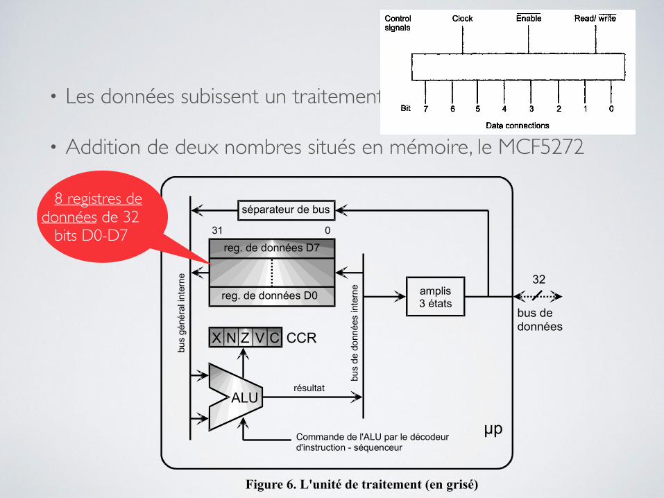
• Les données subissent un traitement
• Addition de deux nombres situés en mémoire, le MCF5272
L’unité de traitement
1.9 Constitution de l’unité de traitement
Les données, échangées par le microprocesseur avec les autres circuits (mémoires et
interfaces), subissent un traitement à l’intérieur du microprocesseur. Par exemple, on peut
envisager l’addition de deux nombres situés en mémoire. Pour cela, le MCF5272 possède 4
éléments8 que l’on peut regrouper dans un bloc fonctionnel nommé unité de traitement (Figure 6) :
• 8 registres de données de 32 bits nommés D0 à D7 ;
• une Unité Arithmétique et Logique (Arithmetic and Logic Unit - ALU) dont le
fonctionnement a été introduit dans la partie 1.8 ;
• un registre CCR (Condition Code Register). Associé à l’ALU, il rend compte du
dernier calcul effectué : génération de retenue, dépassement de capacité… ;
• une unité de multiplication-accumulation spécialement conçue pour le traitement du
signal mais dont nous ne parlerons pas dans ce cours9.
ALU
X N CZ V CCR
amplis3 états
Commande de l'ALU par le décodeurd'instruction - séquenceur
bu
s d
e d
onné
es inte
rne
031
résultat
µp
séparateur de bus
bu
s g
éné
ral in
tern
e
bus dedonnées
32
reg. de données D0
reg. de données D7
Figure 6. L'unité de traitement (en grisé)
8 Le MCF5272 ne possède pas d’unité de virgule flottante (Floating Point Unit - FPU) mais d’autres
microprocesseurs de la famille MCF en sont dotés. La représentation en virgule flottante permet de
représenter des nombres non entiers ayant des ordres de grandeurs très différents. Quand le microprocesseur ne
possède pas de FPU, la représentation des nombres non entiers se fait avec la représentation en virgule fixe mais la plage des nombres représentables est plus restreinte qu’en virgule flottante.9 Cette Multiply / ACcumulate Unit (MAC) réalise les calculs très fréquemment utilisés en traitement du signal.
Ceux-ci sont du type Accumulateur ← Accumulateur + X x Y.
IUT1 de Grenoble – Dpt GEII2 – I2 – Introduction aux systèmes d’informatique industrielle 18
8 registres de données de 32
bits D0-D7
Some more counters, codes and registers - ii i i1!_ i __!11 _ __ !1 _ _ !1 i ii _1 i i l i i i !1 i i i i i i |
Table 16.2 Twisted ring or Johnson counter
After clock pulse
0 (start) 1 2 3 4 5 6 7 8 9
10 11
Qo Q/ Qs
L L L L H H H H H L L L
L L L L L H H H H H L L
. . . and the pattern starts again . . .
Registers A register is just a collection of flip-flops that are used to store or manipulate data in the form of logic 0 and logic 1 levels. With registers it is usually easier to use the alternative form of 1 and 0 rather than high and low levels.
A flip-flop can only store one bit by being set or cleared, so to handle 8 bits at a time we would need eight flip-flops and would refer to this as an 8-bit register. To save space, an 8-bit register would be shown as in Figure 16.3.
Figure 16.3 An 8-bit register
Control Clock Enable Read/ signals
Bit 7 6 5 4 3 2 1 0
Data connections
Note how we number the bits starting at bit 0 rather than refer to the bistable outputs as QA or Qo etc. This is because registers are often used to store data in the form of binary numbers.
2 0 9
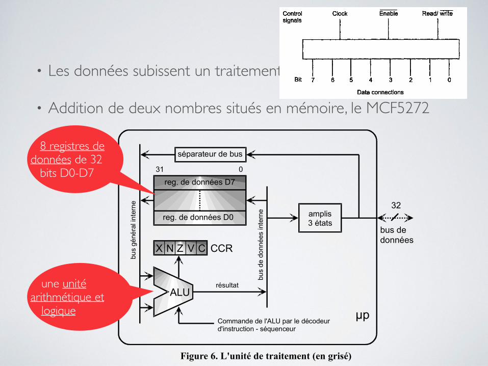
• Les données subissent un traitement
• Addition de deux nombres situés en mémoire, le MCF5272
L’unité de traitement
1.9 Constitution de l’unité de traitement
Les données, échangées par le microprocesseur avec les autres circuits (mémoires et
interfaces), subissent un traitement à l’intérieur du microprocesseur. Par exemple, on peut
envisager l’addition de deux nombres situés en mémoire. Pour cela, le MCF5272 possède 4
éléments8 que l’on peut regrouper dans un bloc fonctionnel nommé unité de traitement (Figure 6) :
• 8 registres de données de 32 bits nommés D0 à D7 ;
• une Unité Arithmétique et Logique (Arithmetic and Logic Unit - ALU) dont le
fonctionnement a été introduit dans la partie 1.8 ;
• un registre CCR (Condition Code Register). Associé à l’ALU, il rend compte du
dernier calcul effectué : génération de retenue, dépassement de capacité… ;
• une unité de multiplication-accumulation spécialement conçue pour le traitement du
signal mais dont nous ne parlerons pas dans ce cours9.
ALU
X N CZ V CCR
amplis3 états
Commande de l'ALU par le décodeurd'instruction - séquenceur
bu
s d
e d
onné
es inte
rne
031
résultat
µp
séparateur de bus
bu
s g
éné
ral in
tern
e
bus dedonnées
32
reg. de données D0
reg. de données D7
Figure 6. L'unité de traitement (en grisé)
8 Le MCF5272 ne possède pas d’unité de virgule flottante (Floating Point Unit - FPU) mais d’autres
microprocesseurs de la famille MCF en sont dotés. La représentation en virgule flottante permet de
représenter des nombres non entiers ayant des ordres de grandeurs très différents. Quand le microprocesseur ne
possède pas de FPU, la représentation des nombres non entiers se fait avec la représentation en virgule fixe mais la plage des nombres représentables est plus restreinte qu’en virgule flottante.9 Cette Multiply / ACcumulate Unit (MAC) réalise les calculs très fréquemment utilisés en traitement du signal.
Ceux-ci sont du type Accumulateur ← Accumulateur + X x Y.
IUT1 de Grenoble – Dpt GEII2 – I2 – Introduction aux systèmes d’informatique industrielle 18
8 registres de données de 32
bits D0-D7
une unité arithmétique et
logique
Some more counters, codes and registers - ii i i1!_ i __!11 _ __ !1 _ _ !1 i ii _1 i i l i i i !1 i i i i i i |
Table 16.2 Twisted ring or Johnson counter
After clock pulse
0 (start) 1 2 3 4 5 6 7 8 9
10 11
Qo Q/ Qs
L L L L H H H H H L L L
L L L L L H H H H H L L
. . . and the pattern starts again . . .
Registers A register is just a collection of flip-flops that are used to store or manipulate data in the form of logic 0 and logic 1 levels. With registers it is usually easier to use the alternative form of 1 and 0 rather than high and low levels.
A flip-flop can only store one bit by being set or cleared, so to handle 8 bits at a time we would need eight flip-flops and would refer to this as an 8-bit register. To save space, an 8-bit register would be shown as in Figure 16.3.
Figure 16.3 An 8-bit register
Control Clock Enable Read/ signals
Bit 7 6 5 4 3 2 1 0
Data connections
Note how we number the bits starting at bit 0 rather than refer to the bistable outputs as QA or Qo etc. This is because registers are often used to store data in the form of binary numbers.
2 0 9
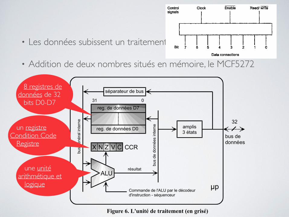
• Les données subissent un traitement
• Addition de deux nombres situés en mémoire, le MCF5272
L’unité de traitement
1.9 Constitution de l’unité de traitement
Les données, échangées par le microprocesseur avec les autres circuits (mémoires et
interfaces), subissent un traitement à l’intérieur du microprocesseur. Par exemple, on peut
envisager l’addition de deux nombres situés en mémoire. Pour cela, le MCF5272 possède 4
éléments8 que l’on peut regrouper dans un bloc fonctionnel nommé unité de traitement (Figure 6) :
• 8 registres de données de 32 bits nommés D0 à D7 ;
• une Unité Arithmétique et Logique (Arithmetic and Logic Unit - ALU) dont le
fonctionnement a été introduit dans la partie 1.8 ;
• un registre CCR (Condition Code Register). Associé à l’ALU, il rend compte du
dernier calcul effectué : génération de retenue, dépassement de capacité… ;
• une unité de multiplication-accumulation spécialement conçue pour le traitement du
signal mais dont nous ne parlerons pas dans ce cours9.
ALU
X N CZ V CCR
amplis3 états
Commande de l'ALU par le décodeurd'instruction - séquenceur
bu
s d
e d
onné
es inte
rne
031
résultat
µp
séparateur de bus
bu
s g
éné
ral in
tern
e
bus dedonnées
32
reg. de données D0
reg. de données D7
Figure 6. L'unité de traitement (en grisé)
8 Le MCF5272 ne possède pas d’unité de virgule flottante (Floating Point Unit - FPU) mais d’autres
microprocesseurs de la famille MCF en sont dotés. La représentation en virgule flottante permet de
représenter des nombres non entiers ayant des ordres de grandeurs très différents. Quand le microprocesseur ne
possède pas de FPU, la représentation des nombres non entiers se fait avec la représentation en virgule fixe mais la plage des nombres représentables est plus restreinte qu’en virgule flottante.9 Cette Multiply / ACcumulate Unit (MAC) réalise les calculs très fréquemment utilisés en traitement du signal.
Ceux-ci sont du type Accumulateur ← Accumulateur + X x Y.
IUT1 de Grenoble – Dpt GEII2 – I2 – Introduction aux systèmes d’informatique industrielle 18
8 registres de données de 32
bits D0-D7
une unité arithmétique et
logique
un registre Condition Code
Registre
Some more counters, codes and registers - ii i i1!_ i __!11 _ __ !1 _ _ !1 i ii _1 i i l i i i !1 i i i i i i |
Table 16.2 Twisted ring or Johnson counter
After clock pulse
0 (start) 1 2 3 4 5 6 7 8 9
10 11
Qo Q/ Qs
L L L L H H H H H L L L
L L L L L H H H H H L L
. . . and the pattern starts again . . .
Registers A register is just a collection of flip-flops that are used to store or manipulate data in the form of logic 0 and logic 1 levels. With registers it is usually easier to use the alternative form of 1 and 0 rather than high and low levels.
A flip-flop can only store one bit by being set or cleared, so to handle 8 bits at a time we would need eight flip-flops and would refer to this as an 8-bit register. To save space, an 8-bit register would be shown as in Figure 16.3.
Figure 16.3 An 8-bit register
Control Clock Enable Read/ signals
Bit 7 6 5 4 3 2 1 0
Data connections
Note how we number the bits starting at bit 0 rather than refer to the bistable outputs as QA or Qo etc. This is because registers are often used to store data in the form of binary numbers.
2 0 9
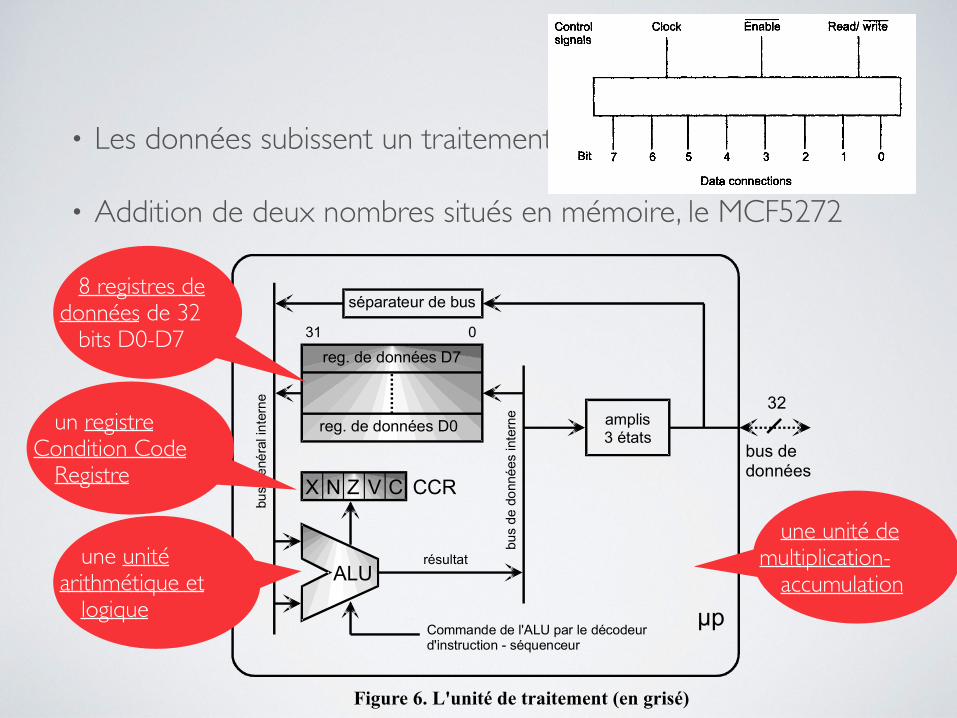
• Les données subissent un traitement
• Addition de deux nombres situés en mémoire, le MCF5272
L’unité de traitement
1.9 Constitution de l’unité de traitement
Les données, échangées par le microprocesseur avec les autres circuits (mémoires et
interfaces), subissent un traitement à l’intérieur du microprocesseur. Par exemple, on peut
envisager l’addition de deux nombres situés en mémoire. Pour cela, le MCF5272 possède 4
éléments8 que l’on peut regrouper dans un bloc fonctionnel nommé unité de traitement (Figure 6) :
• 8 registres de données de 32 bits nommés D0 à D7 ;
• une Unité Arithmétique et Logique (Arithmetic and Logic Unit - ALU) dont le
fonctionnement a été introduit dans la partie 1.8 ;
• un registre CCR (Condition Code Register). Associé à l’ALU, il rend compte du
dernier calcul effectué : génération de retenue, dépassement de capacité… ;
• une unité de multiplication-accumulation spécialement conçue pour le traitement du
signal mais dont nous ne parlerons pas dans ce cours9.
ALU
X N CZ V CCR
amplis3 états
Commande de l'ALU par le décodeurd'instruction - séquenceur
bu
s d
e d
onné
es inte
rne
031
résultat
µp
séparateur de bus
bu
s g
éné
ral in
tern
e
bus dedonnées
32
reg. de données D0
reg. de données D7
Figure 6. L'unité de traitement (en grisé)
8 Le MCF5272 ne possède pas d’unité de virgule flottante (Floating Point Unit - FPU) mais d’autres
microprocesseurs de la famille MCF en sont dotés. La représentation en virgule flottante permet de
représenter des nombres non entiers ayant des ordres de grandeurs très différents. Quand le microprocesseur ne
possède pas de FPU, la représentation des nombres non entiers se fait avec la représentation en virgule fixe mais la plage des nombres représentables est plus restreinte qu’en virgule flottante.9 Cette Multiply / ACcumulate Unit (MAC) réalise les calculs très fréquemment utilisés en traitement du signal.
Ceux-ci sont du type Accumulateur ← Accumulateur + X x Y.
IUT1 de Grenoble – Dpt GEII2 – I2 – Introduction aux systèmes d’informatique industrielle 18
8 registres de données de 32
bits D0-D7
une unité arithmétique et
logique
un registre Condition Code
Registre
une unité de multiplication-
accumulation
Some more counters, codes and registers - ii i i1!_ i __!11 _ __ !1 _ _ !1 i ii _1 i i l i i i !1 i i i i i i |
Table 16.2 Twisted ring or Johnson counter
After clock pulse
0 (start) 1 2 3 4 5 6 7 8 9
10 11
Qo Q/ Qs
L L L L H H H H H L L L
L L L L L H H H H H L L
. . . and the pattern starts again . . .
Registers A register is just a collection of flip-flops that are used to store or manipulate data in the form of logic 0 and logic 1 levels. With registers it is usually easier to use the alternative form of 1 and 0 rather than high and low levels.
A flip-flop can only store one bit by being set or cleared, so to handle 8 bits at a time we would need eight flip-flops and would refer to this as an 8-bit register. To save space, an 8-bit register would be shown as in Figure 16.3.
Figure 16.3 An 8-bit register
Control Clock Enable Read/ signals
Bit 7 6 5 4 3 2 1 0
Data connections
Note how we number the bits starting at bit 0 rather than refer to the bistable outputs as QA or Qo etc. This is because registers are often used to store data in the form of binary numbers.
2 0 9
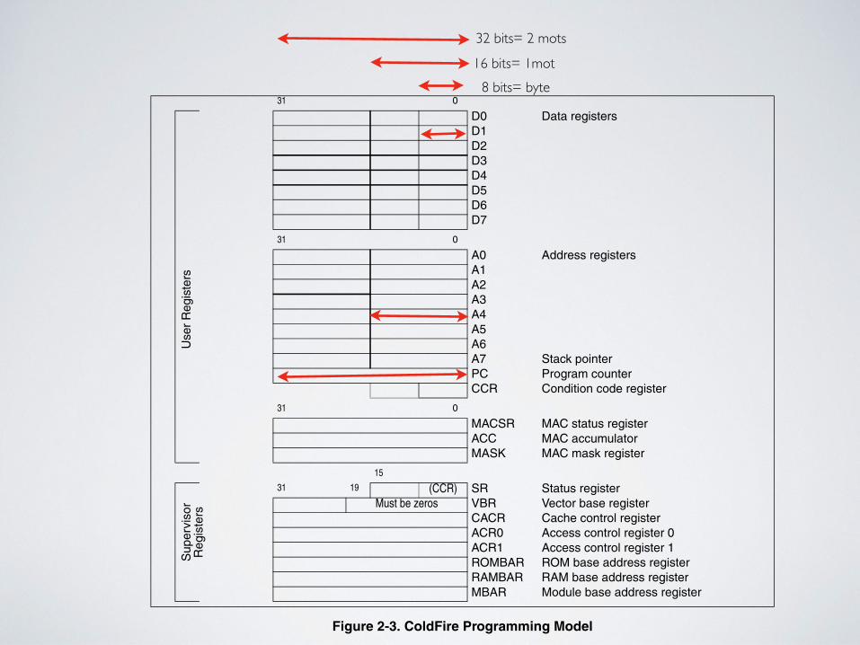
ColdFire Core
MCF5272 ColdFire® Integrated Microprocessor User’s Manual, Rev. 3
Freescale Semiconductor 2-5
Figure 2-3. ColdFire Programming Model
2.2.1.1 Data Registers (D0–D7)
Registers D0–D7 are used as data registers for bit, byte (8-bit), word (16-bit), and longword (32-bit) operations. They may also be used as index registers.
2.2.1.2 Address Registers (A0–A6)
The address registers (A0–A6) can be used as software stack pointers, index registers, or base address registers and may be used for word and longword operations.
2.2.1.3 Stack Pointer (A7, SP)
The processor core supports a single hardware stack pointer (A7) used during stacking for subroutine calls, returns, and exception handling. The stack pointer is implicitly referenced by certain operations and can be explicitly referenced by any instruction specifying an address register. The initial value of A7 is loaded
31 0
D0 Data registersD1D2D3D4D5D6D7
31 0
A0 Address registersA1A2A3A4A5A6A7 Stack pointerPC Program counterCCR Condition code register
31 0
MACSR MAC status registerACC MAC accumulatorMASK MAC mask register
15
31 19 (CCR) SR Status registerMust be zeros VBR Vector base register
CACR Cache control registerACR0 Access control register 0 ACR1 Access control register 1 ROMBAR ROM base address registerRAMBAR RAM base address registerMBAR Module base address register
Use
r Reg
iste
rsS
uper
viso
r R
egis
ters
8 bits= byte16 bits= 1mot
32 bits= 2 mots
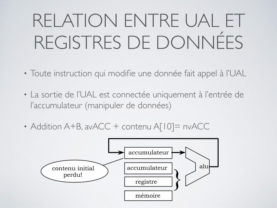
RELATION ENTRE UAL ET REGISTRES DE DONNÉES
• Toute instruction qui modifie une donnée fait appel à l’UAL
• La sortie de l’UAL est connectée uniquement à l’entrée de l’accumulateur (manipuler de données)
• Addition A+B, avACC + contenu A[10]= nvACC
16
L'accumulateur C'est le registre le plus important du microprocesseur, il sert systématiquement lorsque le Pp a besoin de "manipuler" des données. La plupart des opérations logiques et arithmétiques sur les données font appel au couple "UAL - accumulateur" selon la procédure suivante:
accumulateur
accumulateur
registre
mémoire
}alucontenu initial
perdu!
Il en est de même pour les déplacements et transferts des données d'un endroit à un autre comme : de mémoire à mémoire. de mémoire à unités d'entrée-sortie (I/O). Cette action se fait en deux temps :
source vers Accumulateur et ensuite Accumulateur vers destination. Les instructions supportées par un accumulateur sont très nombreuses. Au niveau de la programmation, il représente une grande souplesse d'utilisation! Les autres registres ne permettent que des opérations limitées. Certains microprocesseur, possèdent des accumulateurs de longueur double tel D chez Motorola et HL chez Intel - dissociés en deux et généralement baptisés individuellement A et B ou H et L respectivement. Gros avantage présenté par un Pp possédant plusieurs accumulateurs : les opérations logiques et arithmétiques se font entre accumulateurs limitant ainsi les accès (transferts) avec l'extérieur.
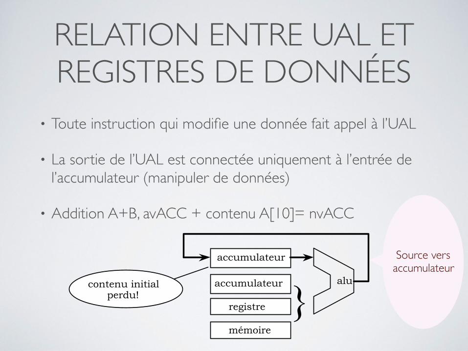
Source vers accumulateur
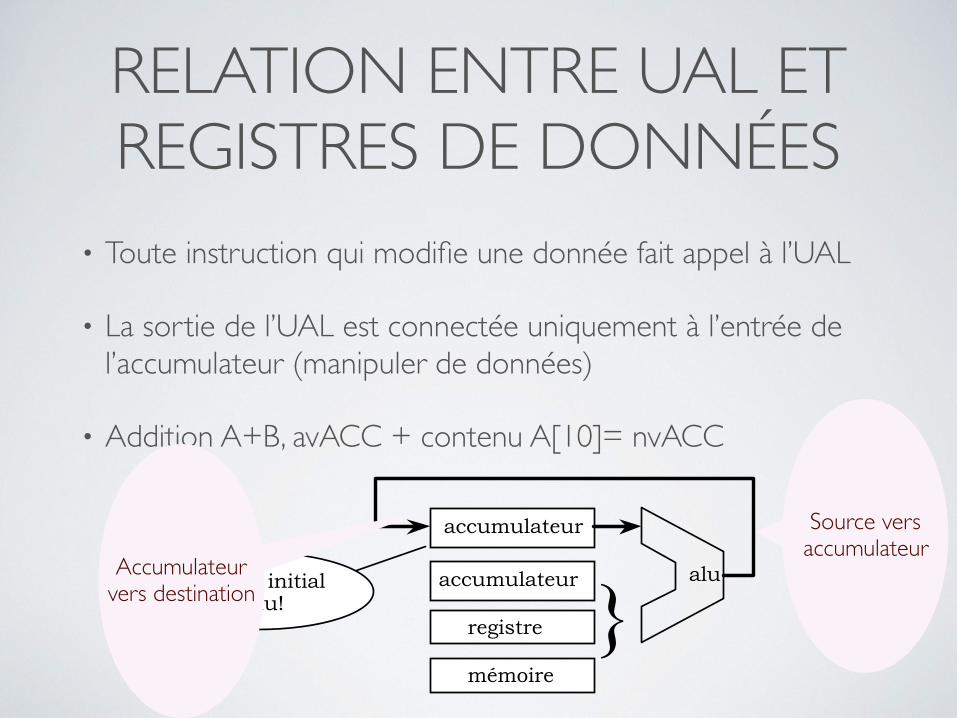
Accumulateur vers destination
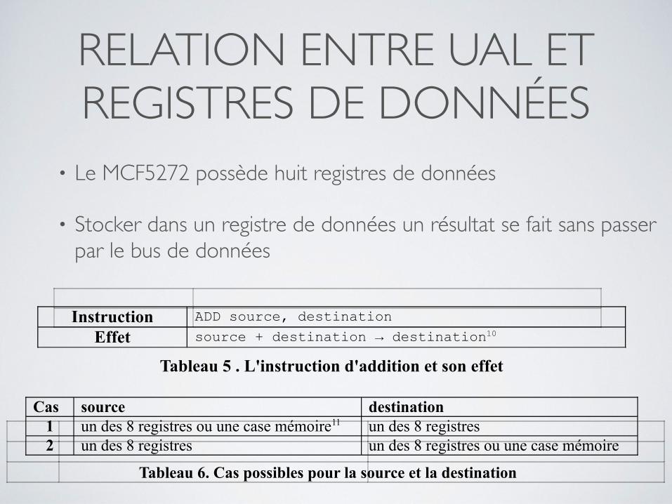
RELATION ENTRE UAL ET REGISTRES DE DONNÉES
• Le MCF5272 possède huit registres de données
• Stocker dans un registre de données un résultat se fait sans passer par le bus de données
1.10Relation entre ALU et registres de données
Examinons dans le paragraphe ci-dessous pourquoi un microprocesseur possède au moins un
registre de données.
Considérons une opération d’addition sur deux opérandes stockés en mémoire de données.
Ces deux opérandes devraient être des entrées de l’ALU. Or le bus de données ne peut
véhiculer qu’une donnée à la fois. C’est pourquoi un microprocesseur possède au moins un registre de données pour garder la mémoire d’un des deux opérandes (il faudra donc
préalablement charger ce registre avec un des deux opérandes). Pour certains
microprocesseurs (premier TP ou architecture PIC par exemple), ce registre de données est
aussi la destination du calcul (là où est stocké le résultat). Ce registre particulier s’appelle
alors l’accumulateur. Le calcul réalisé est du type :
ancienne valeur de l’acc. + contenu d’une case mémoire→ nouvelle valeur de l’acc.
Le MCF5272 présente plus de souplesse puisqu’il possède huit registres de données qui
peuvent être utilisés de différentes façons. Reprenons notre exemple de l’addition. Le Tableau
5 donne l’instruction correspondante et son effet.
Instruction ADD source, destination
Effet source + destination → destination10
Tableau 5 . L'instruction d'addition et son effet
Les cas possibles pour la source et la destination sont donnés dans le Tableau 6.
Cas source destination1 un des 8 registres ou une case mémoire11 un des 8 registres
2 un des 8 registres un des 8 registres ou une case mémoire
Tableau 6. Cas possibles pour la source et la destination
En outre, les données issues des registres de données et allant vers l’ALU n’empruntent pas le
bus de données. Cela procure une grande rapidité. De même, stocker dans un registre de
données un résultat produit par l’ALU se fait sans passer par le bus de données.
1.11 Le Condition Code Register (CCR)
Le résultat d’un calcul peut être positif ou négatif, nul, à l’origine d’un retenue, ou encore
générer un débordement. La connaissance de ces événements peut être utile pour, par
exemple, dérouter le programme. La Figure 7 est un extrait de la documentation du MCF5272
expliquant le positionnement des drapeaux témoignant de ces événements. Ces drapeaux
(flags) sont représentés chacun par un bit et sont regroupés dans le Condition Code Register.
L’exécution de chaque instruction repositionne les bits de ce registre selon des modalités
définies dans la documentation des instructions. Sur la , on trouve par exemple l’état du CCR
après l’exécution de l’instruction ADD.
Le CCR représente en fait les 8 bits de poids faible d’un registre de 16 bits appelé le registre d’état (Status Register - SR). Les flags X, N, Z, V et C sont d’ailleurs aussi appelés bits d’état.
10 On s’aperçoit qu’un des deux opérandes sera nécessairement « écrasé » par la destination.11 En fait ce sera une, deux ou quatre cases mémoires de 8 bits selon que l’on manipule des octets (8 bits), des
mots (16 bits) ou des longs mots (32 bits).
IUT1 de Grenoble – Dpt GEII2 – I2 – Introduction aux systèmes d’informatique industrielle 19
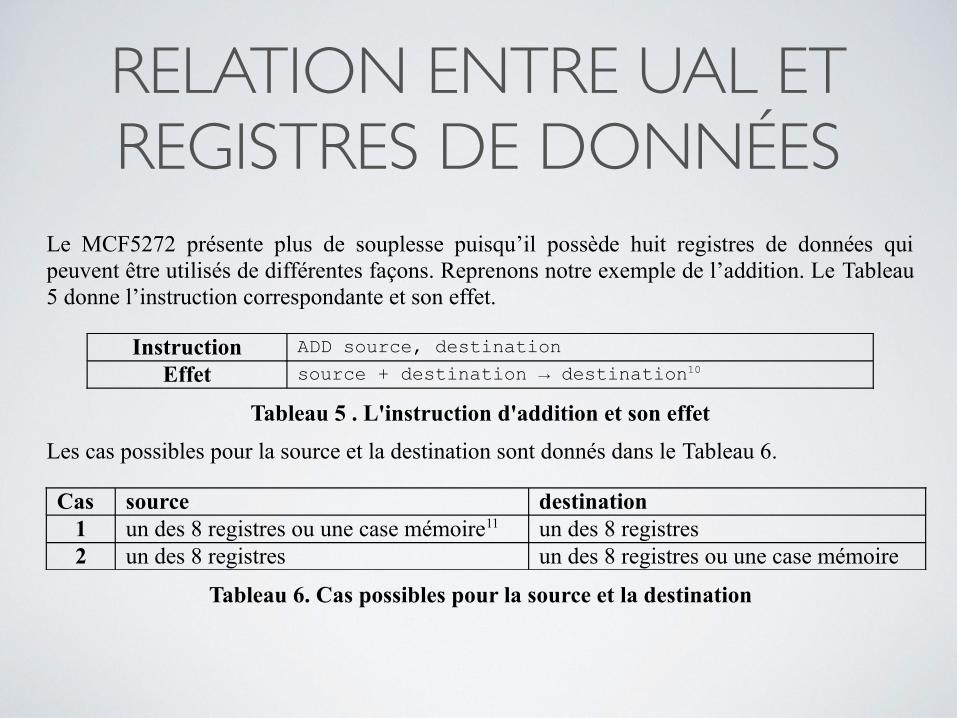
RELATION ENTRE UAL ET REGISTRES DE DONNÉES
1.10Relation entre ALU et registres de données
Examinons dans le paragraphe ci-dessous pourquoi un microprocesseur possède au moins un
registre de données.
Considérons une opération d’addition sur deux opérandes stockés en mémoire de données.
Ces deux opérandes devraient être des entrées de l’ALU. Or le bus de données ne peut
véhiculer qu’une donnée à la fois. C’est pourquoi un microprocesseur possède au moins un registre de données pour garder la mémoire d’un des deux opérandes (il faudra donc
préalablement charger ce registre avec un des deux opérandes). Pour certains
microprocesseurs (premier TP ou architecture PIC par exemple), ce registre de données est
aussi la destination du calcul (là où est stocké le résultat). Ce registre particulier s’appelle
alors l’accumulateur. Le calcul réalisé est du type :
ancienne valeur de l’acc. + contenu d’une case mémoire→ nouvelle valeur de l’acc.
Le MCF5272 présente plus de souplesse puisqu’il possède huit registres de données qui
peuvent être utilisés de différentes façons. Reprenons notre exemple de l’addition. Le Tableau
5 donne l’instruction correspondante et son effet.
Instruction ADD source, destination
Effet source + destination → destination10
Tableau 5 . L'instruction d'addition et son effet
Les cas possibles pour la source et la destination sont donnés dans le Tableau 6.
Cas source destination1 un des 8 registres ou une case mémoire11 un des 8 registres
2 un des 8 registres un des 8 registres ou une case mémoire
Tableau 6. Cas possibles pour la source et la destination
En outre, les données issues des registres de données et allant vers l’ALU n’empruntent pas le
bus de données. Cela procure une grande rapidité. De même, stocker dans un registre de
données un résultat produit par l’ALU se fait sans passer par le bus de données.
1.11 Le Condition Code Register (CCR)
Le résultat d’un calcul peut être positif ou négatif, nul, à l’origine d’un retenue, ou encore
générer un débordement. La connaissance de ces événements peut être utile pour, par
exemple, dérouter le programme. La Figure 7 est un extrait de la documentation du MCF5272
expliquant le positionnement des drapeaux témoignant de ces événements. Ces drapeaux
(flags) sont représentés chacun par un bit et sont regroupés dans le Condition Code Register.
L’exécution de chaque instruction repositionne les bits de ce registre selon des modalités
définies dans la documentation des instructions. Sur la , on trouve par exemple l’état du CCR
après l’exécution de l’instruction ADD.
Le CCR représente en fait les 8 bits de poids faible d’un registre de 16 bits appelé le registre d’état (Status Register - SR). Les flags X, N, Z, V et C sont d’ailleurs aussi appelés bits d’état.
10 On s’aperçoit qu’un des deux opérandes sera nécessairement « écrasé » par la destination.11 En fait ce sera une, deux ou quatre cases mémoires de 8 bits selon que l’on manipule des octets (8 bits), des
mots (16 bits) ou des longs mots (32 bits).
IUT1 de Grenoble – Dpt GEII2 – I2 – Introduction aux systèmes d’informatique industrielle 19

LE REGISTRE D’ADRESSE• Sert d’interface entre le bus de données interne et le bus des
adresses, il pilote le bus d’adresse
• Son contenu provient des différentes sources:
• Le compteur d’instruction
• Un registre général
• Un emplacement mémoire
• Le contenu du registre d’adresse pointe la zone mémoire utile au uP
LE REGISTRE D’INSTRUCTION
• Contient le code de l’instruction en cours d’exécution
• Ceci indique au microprocesseur deux choses :
• Une action (une lecture, une écriture ou autre ...)
• Un lieu d'action (un registre, un accumulateur, une case mémoire...)
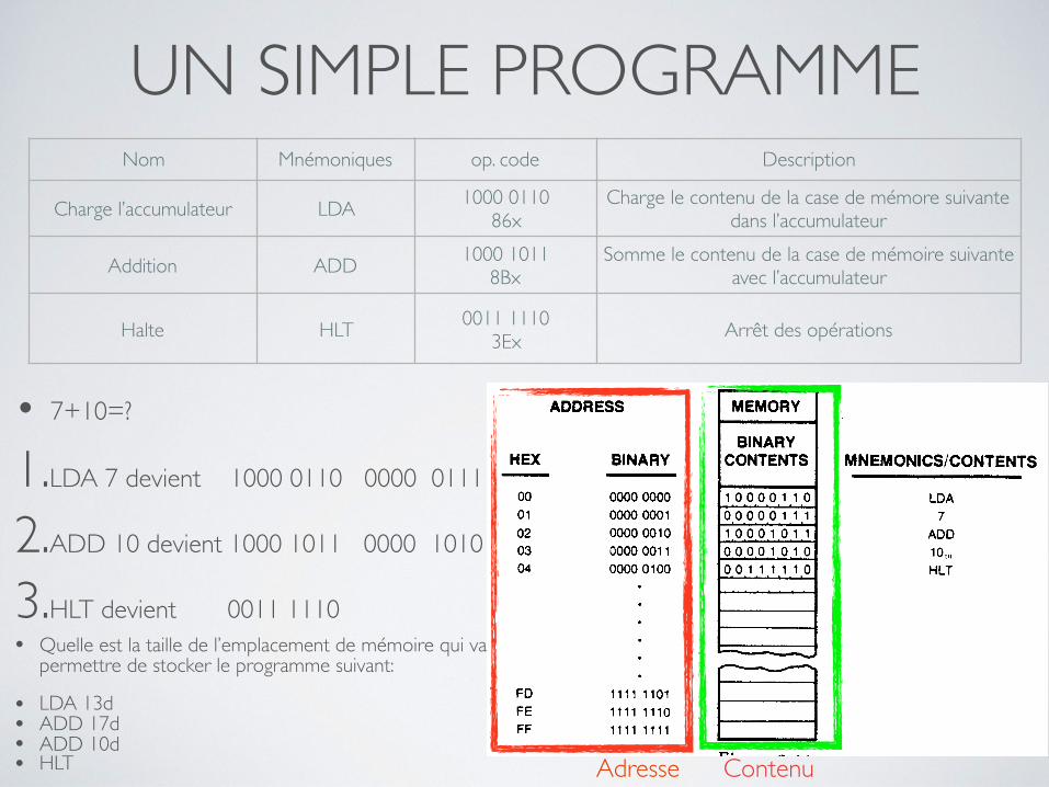
UN SIMPLE PROGRAMME
• 7+10=?
1.LDA 7 devient 1000 0110 0000 0111
2.ADD 10 devient 1000 1011 0000 1010
3.HLT devient 0011 1110
Nom Mnémoniques op. code Description
Charge l’accumulateur LDA 1000 011086x
Charge le contenu de la case de mémore suivante dans l’accumulateur
Addition ADD 1000 10118Bx
Somme le contenu de la case de mémoire suivante avec l’accumulateur
Halte HLT 0011 11103Ex Arrêt des opérations
Adresse Contenu
• Quelle est la taille de l’emplacement de mémoire qui va permettre de stocker le programme suivant:
• LDA 13d• ADD 17d• ADD 10d• HLT
PHASE DE FETCH
PHASE DE FETCH
Le PC est incrémenté 01
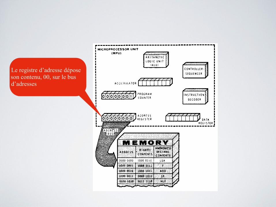
Le registre d’adresse dépose son contenu, 00, sur le bus d’adresses
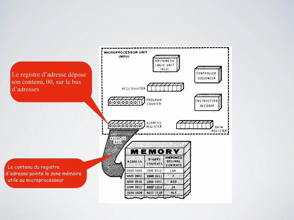
Le contenu du registre d'adresse pointe la zone mémoire utile au microprocesseur
Le registre d’adresse dépose son contenu, 00, sur le bus d’adresses
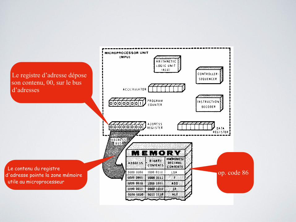
Le contenu du registre d'adresse pointe la zone mémoire utile au microprocesseur
op. code 86
Le registre d’adresse dépose son contenu, 00, sur le bus d’adresses
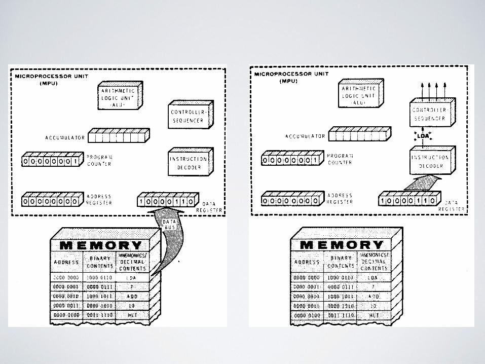
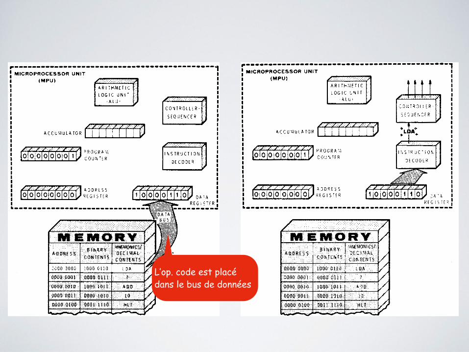
L’op. code est placé dans le bus de données
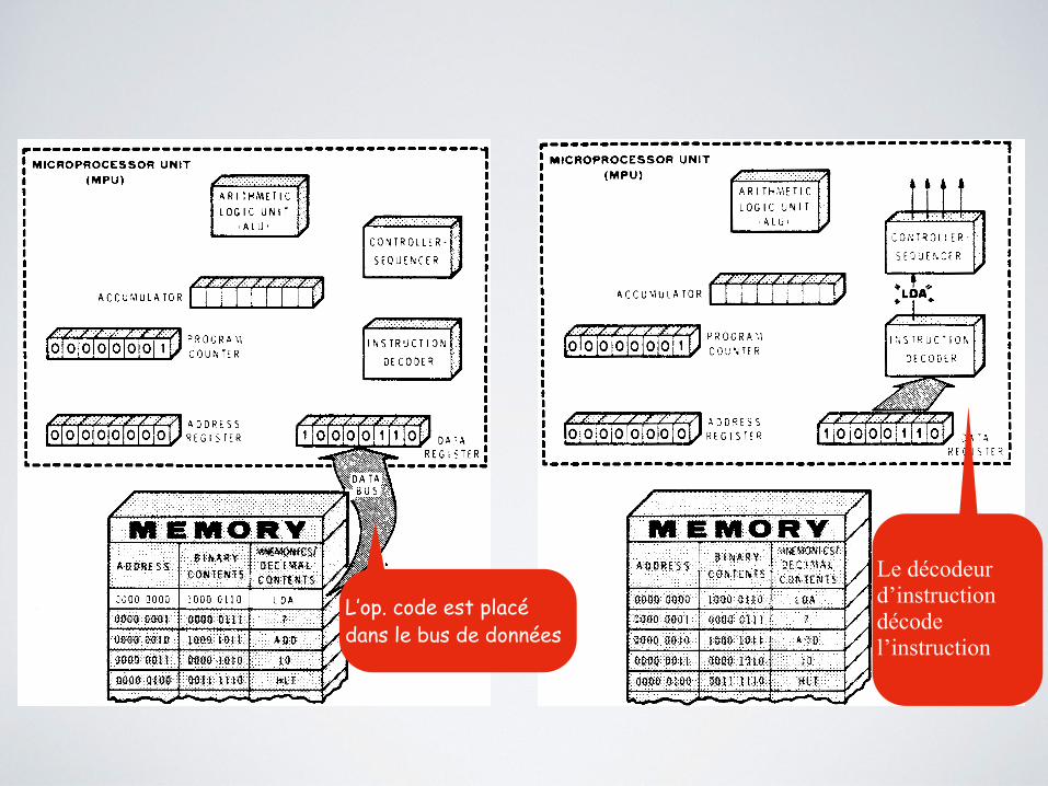
Le décodeur d’instruction décode l’instruction
L’op. code est placé dans le bus de données
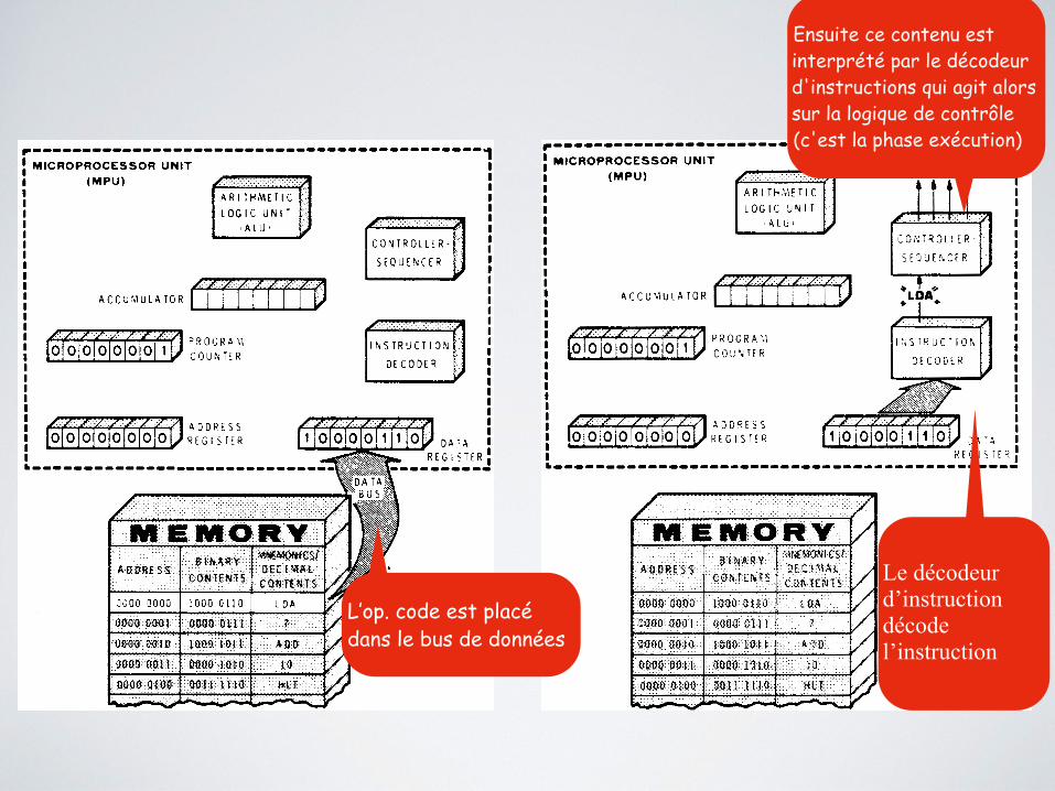
Le décodeur d’instruction décode l’instruction
L’op. code est placé dans le bus de données
Ensuite ce contenu est interprété par le décodeur d'instructions qui agit alors sur la logique de contrôle (c'est la phase exécution)
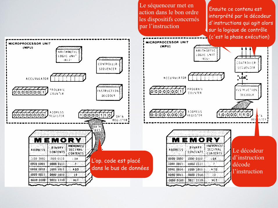
Le décodeur d’instruction décode l’instruction
Le séquenceur met en action dans le bon ordre les dispositifs concernés par l’instruction
L’op. code est placé dans le bus de données
Ensuite ce contenu est interprété par le décodeur d'instructions qui agit alors sur la logique de contrôle (c'est la phase exécution)
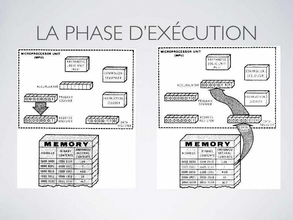
LA PHASE D’EXÉCUTION
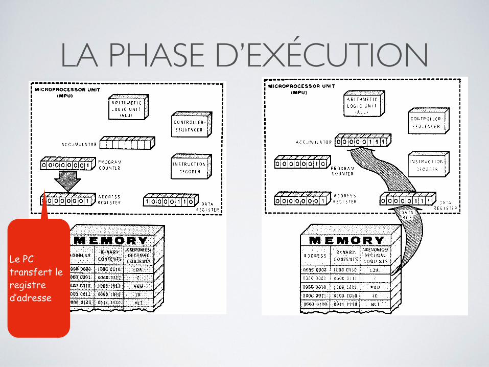
LA PHASE D’EXÉCUTION
Le PC transfert le registre d’adresse
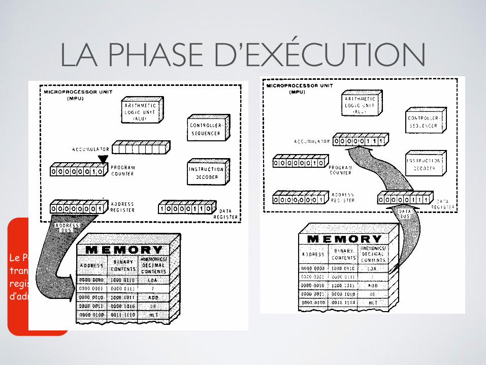
LA PHASE D’EXÉCUTION
Le PC transfert le registre d’adresse
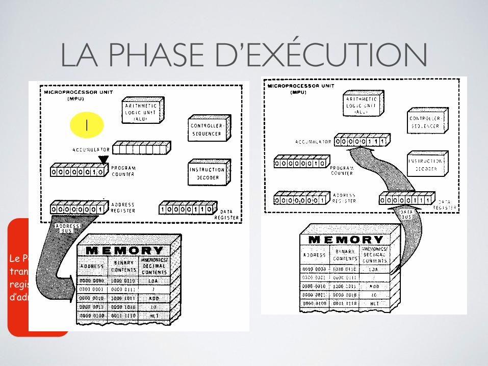
LA PHASE D’EXÉCUTION
Le PC transfert le registre d’adresse
1
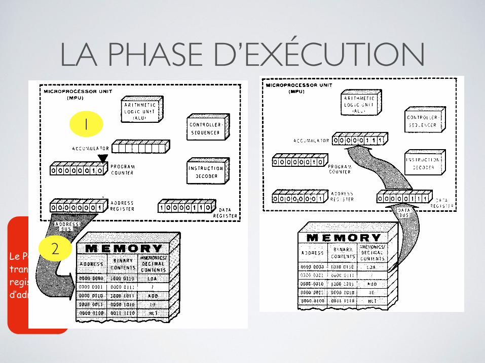
LA PHASE D’EXÉCUTION
Le PC transfert le registre d’adresse
1
2
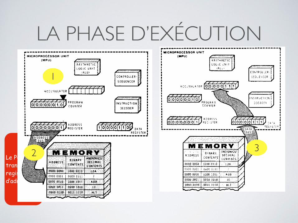
LA PHASE D’EXÉCUTION
Le PC transfert le registre d’adresse
1
2 3
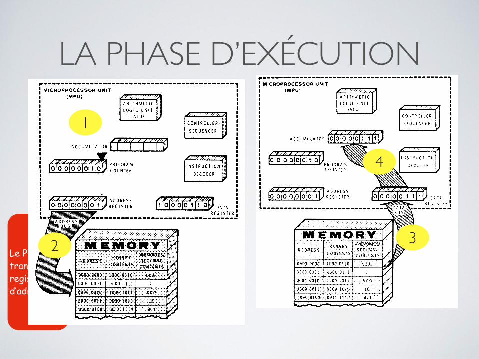
LA PHASE D’EXÉCUTION
Le PC transfert le registre d’adresse
1
2 3
4
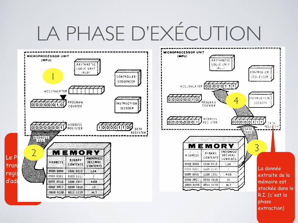
LA PHASE D’EXÉCUTION
Le PC transfert le registre d’adresse
1
2 3
4
La donnée extraite de la mémoire est stockée dans le R.I. (c'est la phase extraction)
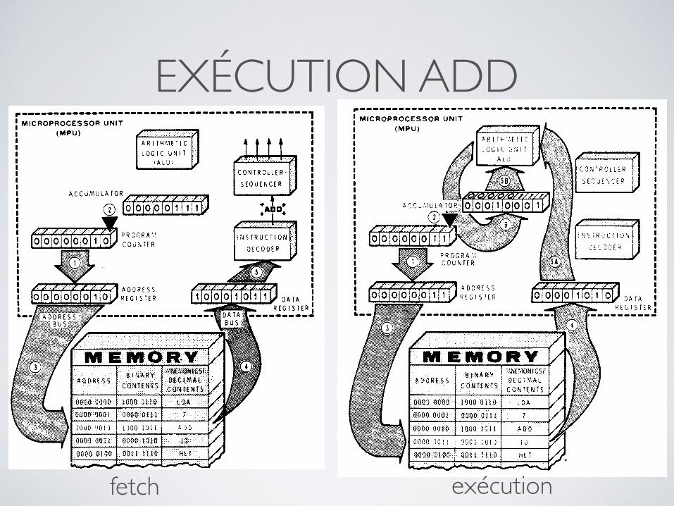
EXÉCUTION ADD
fetch exécution
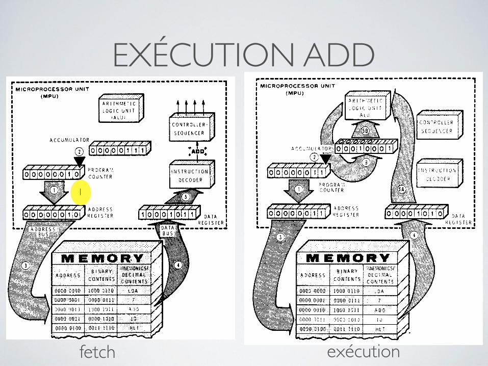
EXÉCUTION ADD
fetch exécution
1
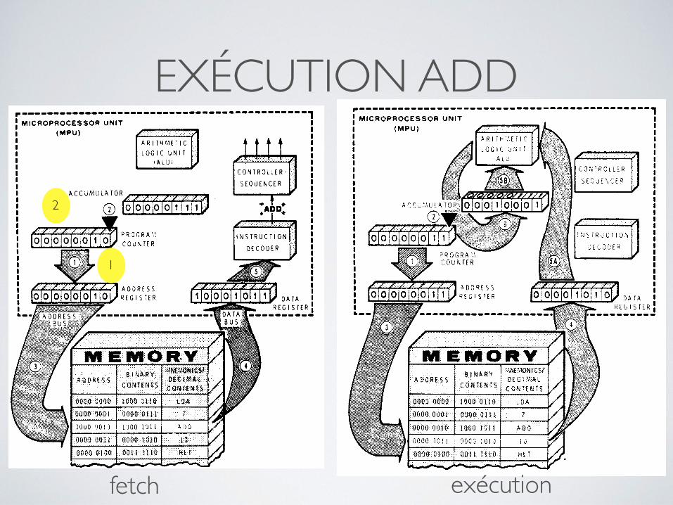
EXÉCUTION ADD
fetch exécution
1
2
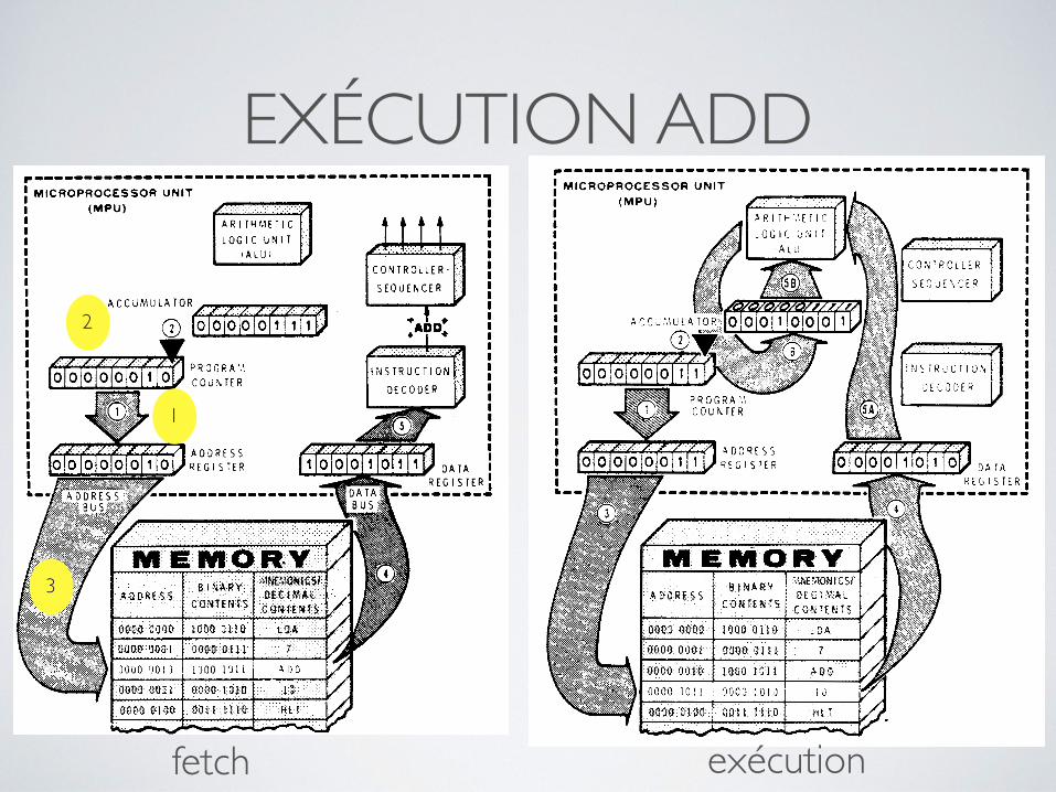
EXÉCUTION ADD
fetch exécution
1
2
3
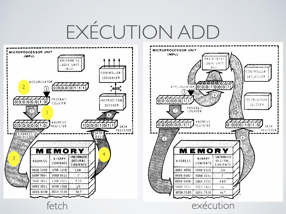
EXÉCUTION ADD
fetch exécution
1
2
34
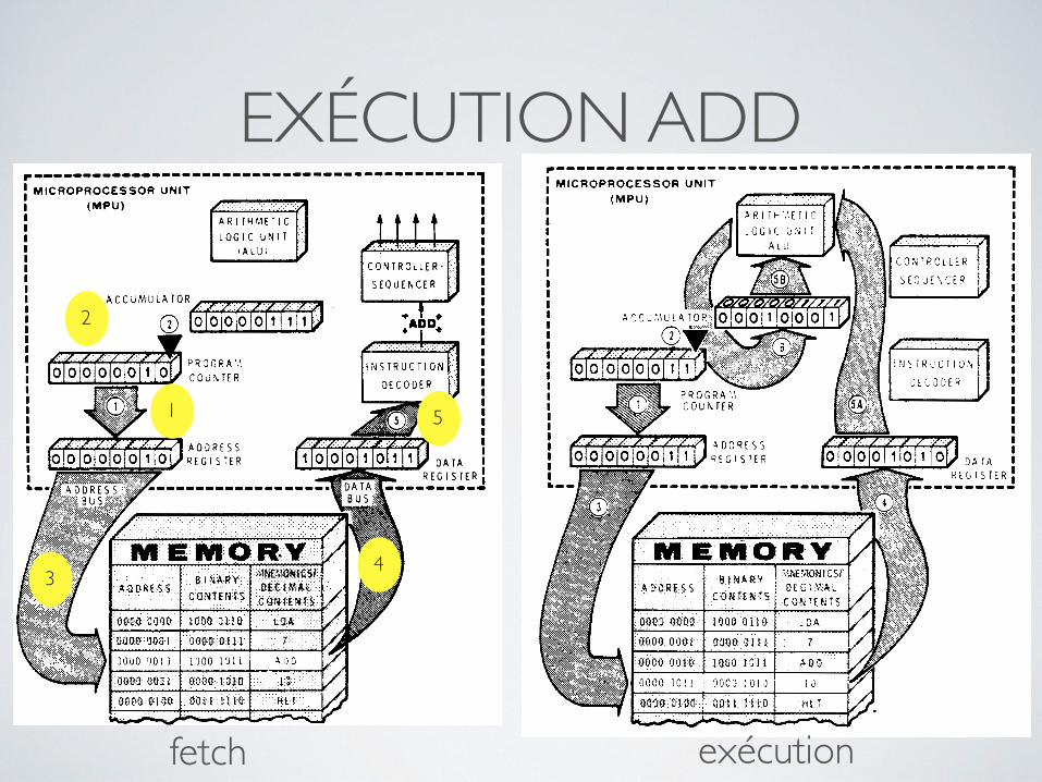
EXÉCUTION ADD
fetch exécution
1
2
34
5
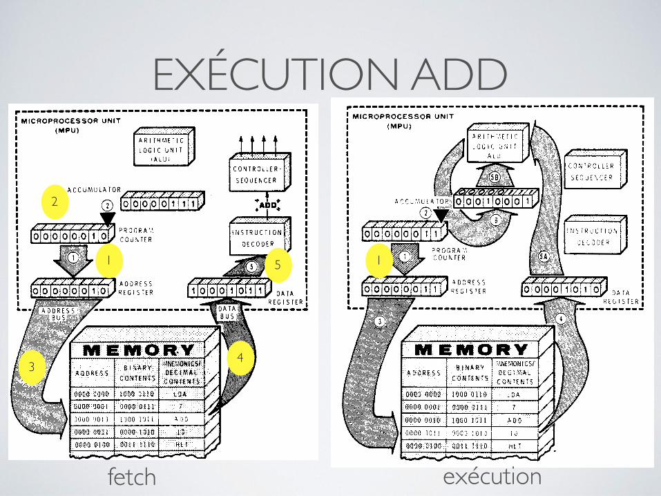
EXÉCUTION ADD
fetch exécution
1
2
34
5 1
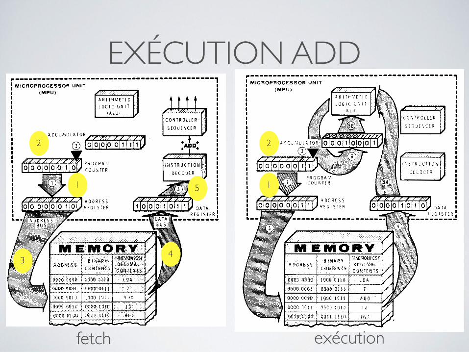
EXÉCUTION ADD
fetch exécution
1
2
34
5 1
2
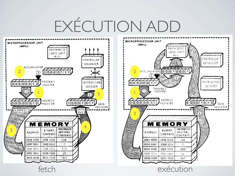
EXÉCUTION ADD
fetch exécution
1
2
34
5 1
2
3
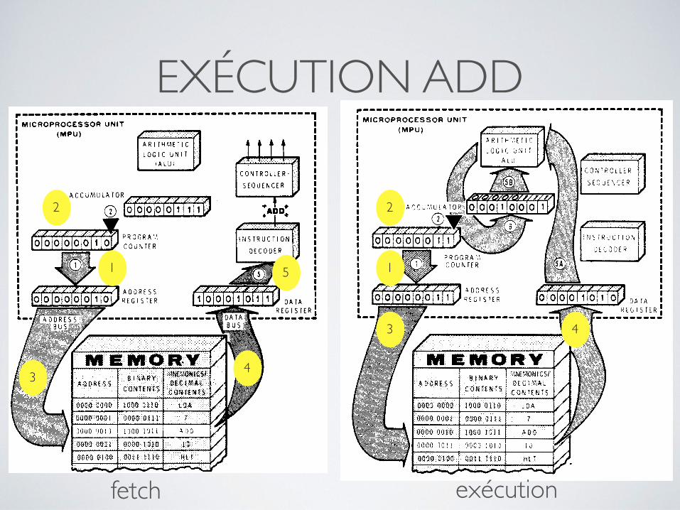
EXÉCUTION ADD
fetch exécution
1
2
34
5 1
2
3 4
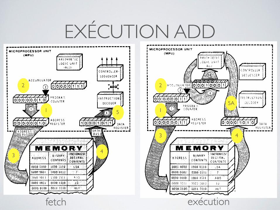
EXÉCUTION ADD
fetch exécution
1
2
34
5 1
2
3 4
5A
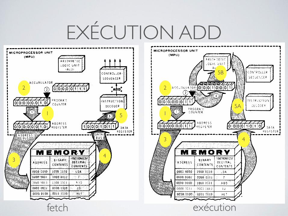
EXÉCUTION ADD
fetch exécution
1
2
34
5 1
2
3 4
5A
5B
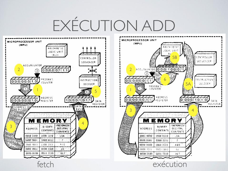
EXÉCUTION ADD
fetch exécution
1
2
34
5 1
2
3 4
5A
5B
6
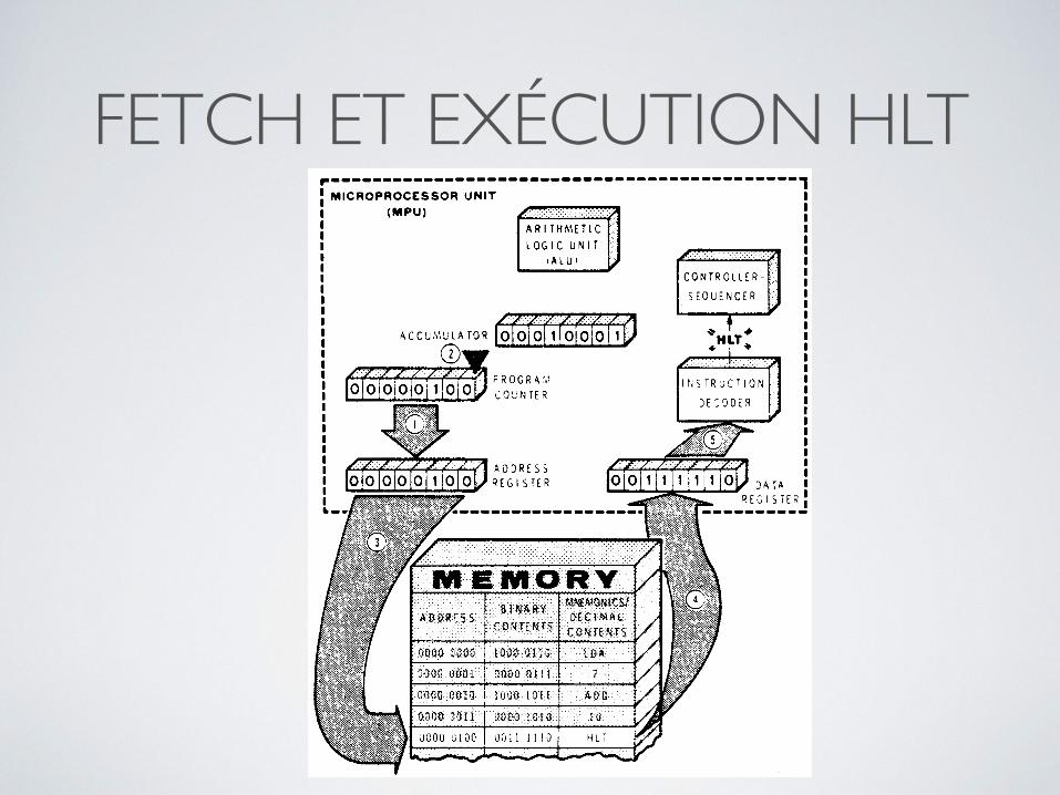
FETCH ET EXÉCUTION HLT
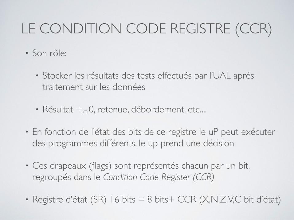
LE CONDITION CODE REGISTRE (CCR)• Son rôle:
• Stocker les résultats des tests effectués par l’UAL après traitement sur les données
• Résultat +,-,0, retenue, débordement, etc....
• En fonction de l’état des bits de ce registre le uP peut exécuter des programmes différents, le up prend une décision
• Ces drapeaux (flags) sont représentés chacun par un bit, regroupés dans le Condition Code Register (CCR)
• Registre d’état (SR) 16 bits = 8 bits+ CCR (X,N,Z,V,C bit d’état)
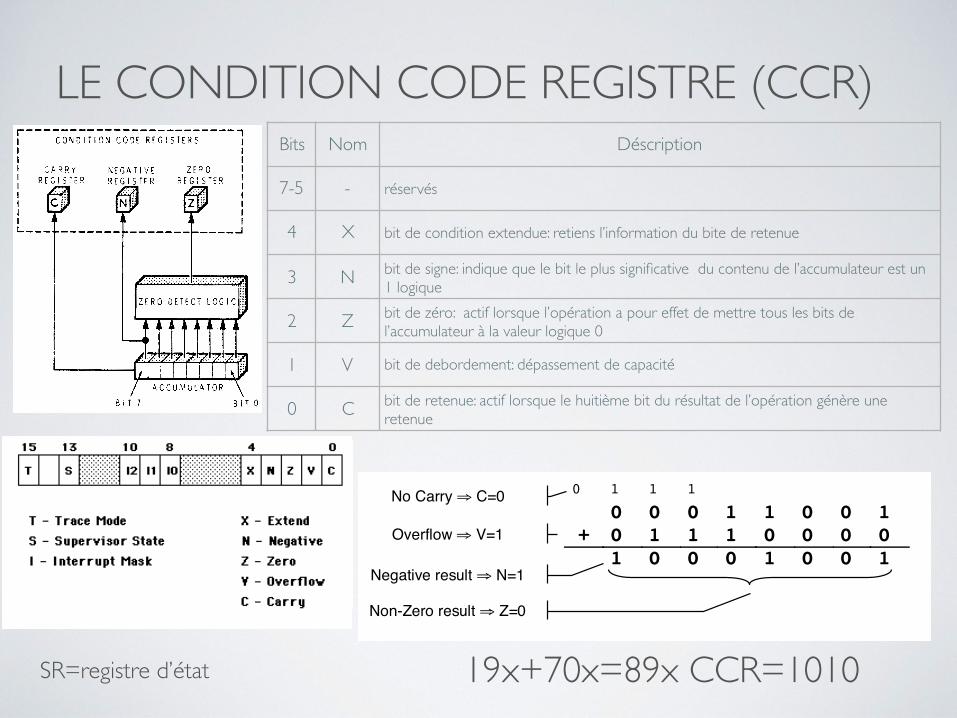
Microprocessor-based System DesignRicardo Gutierrez-OsunaWright State University
5
Status/Condition Code Register
More significant byte: SROnly modifiable in supervisor modeDetails in later sections
Least significant byte: CCRFor user-level programsBehavior depends on instruction
Bit MeaningT Tracing for run-time
debuggingS Supervisor or
User ModeI System responds to interrupts
with a level higher than IC Set if a carry or borrow is
generated. Cleared otherwiseV Set if a signed overflow
occurs. Cleared otherwiseZ Set if the result is zero.
Cleared otherwiseN Set if the result is negative.
Cleared otherwiseX Retains information from the carry
bit for multi-precision arithmetic
LE CONDITION CODE REGISTRE (CCR)
Microprocessor-based System DesignRicardo Gutierrez-OsunaWright State University
6
Condition Code Register exampleAdd the numbers $19 and $70 and show the effect on the CCR bits
The following piece of code performs the operationMOVE.B #$70,D0ADD.B #$19,DO
To illustrate the behavior of the CCR we will perform an addition in base 2
0 1 1 10 0 0 1 1 0 0 1
+ 0 1 1 1 0 0 0 01 0 0 0 1 0 0 1
Negative result ⇒ N=1
No Carry ⇒ C=0
Non-Zero result ⇒ Z=0
Overflow ⇒ V=1
19x+70x=89x CCR=1010
Bits Nom Déscription
7-5 - réservés
4 X bit de condition extendue: retiens l’information du bite de retenue
3 N bit de signe: indique que le bit le plus significative du contenu de l’accumulateur est un 1 logique
2 Z bit de zéro: actif lorsque l’opération a pour effet de mettre tous les bits de l’accumulateur à la valeur logique 0
1 V bit de debordement: dépassement de capacité
0 C bit de retenue: actif lorsque le huitième bit du résultat de l’opération génère une retenue
SR=registre d’état
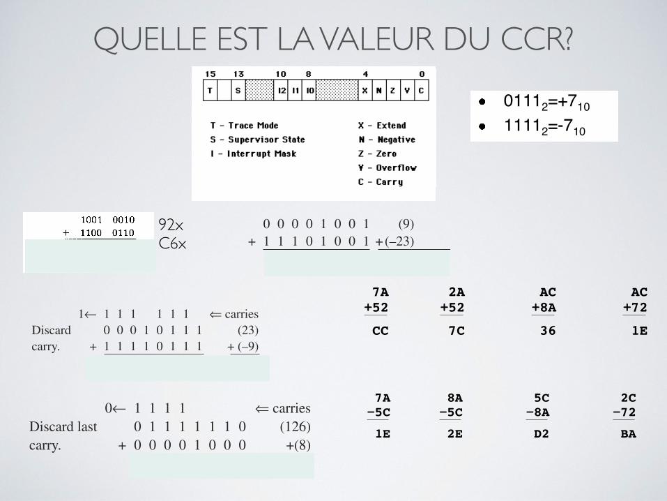
QUELLE EST LA VALEUR DU CCR?
Microprocessor-based System DesignRicardo Gutierrez-OsunaWright State University
5
Status/Condition Code Register
More significant byte: SROnly modifiable in supervisor modeDetails in later sections
Least significant byte: CCRFor user-level programsBehavior depends on instruction
Bit MeaningT Tracing for run-time
debuggingS Supervisor or
User ModeI System responds to interrupts
with a level higher than IC Set if a carry or borrow is
generated. Cleared otherwiseV Set if a signed overflow
occurs. Cleared otherwiseZ Set if the result is zero.
Cleared otherwiseN Set if the result is negative.
Cleared otherwiseX Retains information from the carry
bit for multi-precision arithmetic
92xC6x
Microprocessor-based System DesignRicardo Gutierrez-OsunaWright State University
8
2’s complement (review)How to express negative numbers in binary?
Sign-Magnitude:Use the Most Significant Bit to encode the sign
01112=+71011112=-710
2s Complement:The most commonly used form
Subtraction is made very easy (perform the operation 5-7)The range of numbers that can be represented is from -2n-1 to +2n-1-1
Binary number (+510) 0 0 0 0 0 1 0 1↓ ↓ ↓ ↓ ↓ ↓ ↓ ↓
1s complement 1 1 1 1 1 0 1 0Add 1 + 1
2s complement (-510) 1 1 1 1 1 0 1 1
2.4 / Signed Integer Representation 53
It is left as an exercise for you to verify that 111100102 is actually !1410 usingtwo’s complement notation.
EXAMPLE 2.21 Find the sum of 2310 and !910 in binary using two’s comple-ment arithmetic.
1← 1 1 1 1 1 1 ⇐ carriesDiscard 0 0 0 1 0 1 1 1 (23)carry. + 1 1 1 1 0 1 1 1 + (–9)
0 0 0 0 1 1 1 0 1410
Notice that the discarded carry in Example 2.21 did not cause an erroneous result.An overflow occurs if two positive numbers are added and the result is negative,or if two negative numbers are added and the result is positive. It is not possibleto have overflow when using two’s complement notation if a positive and a nega-tive number are being added together.
Simple computer circuits can easily detect an overflow condition using a rulethat is easy to remember. You’ll notice in Example 2.21 that the carry going intothe sign bit (a 1 is carried from the previous bit position into the sign bit position)is the same as the carry going out of the sign bit (a 1 is carried out and discarded).When these carries are equal, no overflow occurs. When they differ, an overflowindicator is set in the arithmetic logic unit, indicating the result is incorrect.
A Simple Rule for Detecting an Overflow Condition: If the carry intothe sign bit equals the carry out of the bit, no overflow has occurred. Ifthe carry into the sign bit is different from the carry out of the sign bit,overflow (and thus an error) has occurred.
The hard part is getting programmers (or compilers) to consistently check for theoverflow condition. Example 2.22 indicates overflow because the carry into the signbit (a 1 is carried in) is not equal to the carry out of the sign bit (a 0 is carried out).
EXAMPLE 2.22 Find the sum of 12610 and 810 in binary using two’s comple-ment arithmetic.
0← 1 1 1 1 ⇐ carriesDiscard last 0 1 1 1 1 1 1 0 (126)carry. + 0 0 0 0 1 0 0 0 +(8)
1 0 0 0 0 1 1 0 (–122???)
52 Chapter 2 / Data Representation in Computer Systems
as well. Since the subtrahend (the number we complement and add) is incre-mented at the outset, however, there is no end carry-around to worry about. Wesimply discard any carries involving the high-order bits. Remember, only negativenumbers need to be converted to two’s complement notation, as indicated inExample 2.19.
EXAMPLE 2.19 Express 2310, !2310, and !910 in 8-bit binary two’s comple-ment form.
2310 = + (000101112) = 000101112!2310 = ! (000101112) = 111010002 + 1 = 111010012
!910 = ! (000010012) = 111101102 + 1 = 111101112
Suppose we are given the binary representation for a number and want to knowits decimal equivalent? Positive numbers are easy. For example, to convert thetwo’s complement value of 000101112 to decimal, we simply convert this binarynumber to a decimal number to get 23. However, converting two’s complementnegative numbers requires a reverse procedure similar to the conversion fromdecimal to binary. Suppose we are given the two’s complement binary value of111101112, and we want to know the decimal equivalent. We know this is a nega-tive number but must remember it is represented using two’s complement. Wefirst flip the bits and then add 1 (find the one’s complement and add 1). Thisresults in the following: 000010002 + 1 = 000010012. This is equivalent to thedecimal value 9. However, the original number we started with was negative, sowe end up with !9 as the decimal equivalent to 111101112.
The following two examples illustrate how to perform addition (and hencesubtraction, because we subtract a number by adding its opposite) using two’scomplement notation.
EXAMPLE 2.20 Add 910 to !2310 using two’s complement arithmetic.
0 0 0 0 1 0 0 1 (9)+ 1 1 1 0 1 0 0 1 +(–23)
1 1 1 1 0 0 1 0 –1410
EE 308 Spring 2002
Addition of hexadecimal numbers
ADDITION:
C bit set when result does not fit in word
V bit set when P + P = N N + N = P
7A+52 CC
+52 2A
7C+8A AC
36+72 AC
1E
N bit set when MSB of result is 1
Z bit set when result is 0
C: 0 C: 1
V: 0
C: 0
V: 1
C: 1
V: 1 V: 0
N: 1 N: 0 N: 1
Z: 0 Z: 0 Z: 0
N: 0
Z: 0
2
EE 308 Spring 2002
Subtraction of hexadecimal numbers
SUBTRACTION:
C bit set on borrow (when the magnitude of the subtrahend
V bit set when N − P = P P − N = N
is greater than the minuend)
7A−5C 1E
−5C 8A
2E
5C−8A D2
2C−72 BA
C: 0
V: 0
C: 1
V: 0
C: 0
V: 1V: 1
C: 1
N: 0 N: 0 N: 1 N: 1
Z: 0Z: 0Z: 0Z: 0
N bit set when MSB is 1Z bit set when result is 0
3
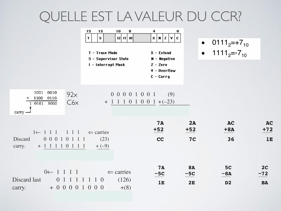
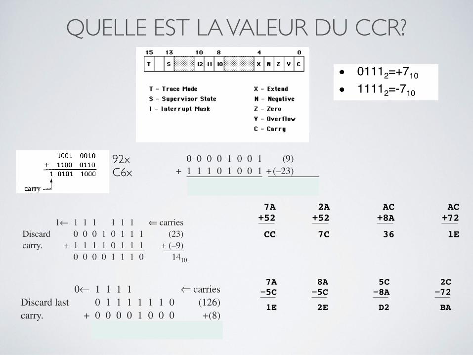
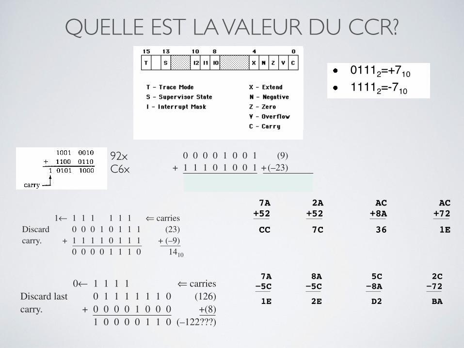
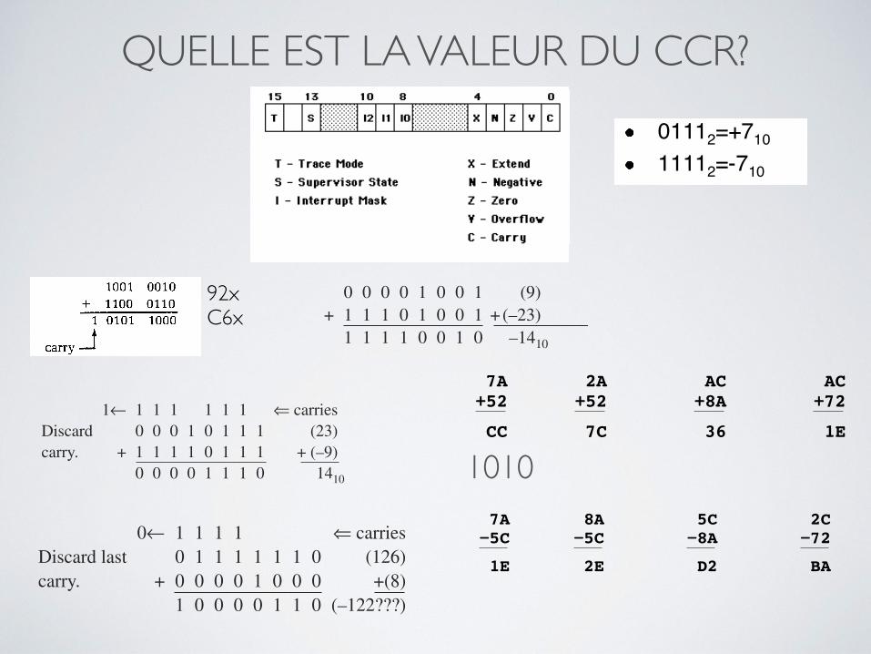
1010
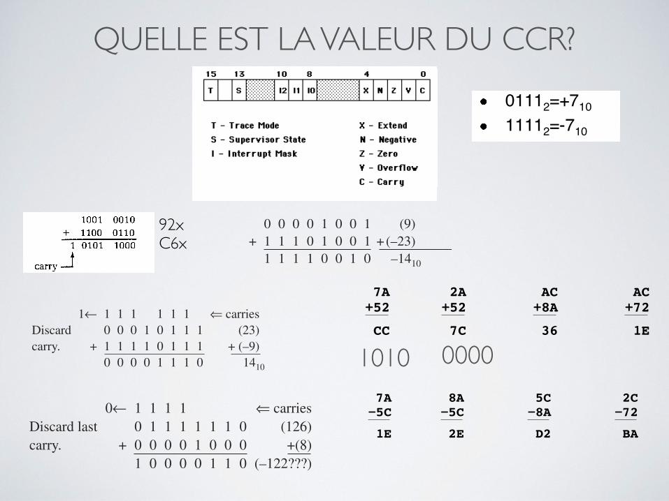
QUELLE EST LA VALEUR DU CCR?
Microprocessor-based System DesignRicardo Gutierrez-OsunaWright State University
5
Status/Condition Code Register
More significant byte: SROnly modifiable in supervisor modeDetails in later sections
Least significant byte: CCRFor user-level programsBehavior depends on instruction
Bit MeaningT Tracing for run-time
debuggingS Supervisor or
User ModeI System responds to interrupts
with a level higher than IC Set if a carry or borrow is
generated. Cleared otherwiseV Set if a signed overflow
occurs. Cleared otherwiseZ Set if the result is zero.
Cleared otherwiseN Set if the result is negative.
Cleared otherwiseX Retains information from the carry
bit for multi-precision arithmetic
92xC6x
Microprocessor-based System DesignRicardo Gutierrez-OsunaWright State University
8
2’s complement (review)How to express negative numbers in binary?
Sign-Magnitude:Use the Most Significant Bit to encode the sign
01112=+71011112=-710
2s Complement:The most commonly used form
Subtraction is made very easy (perform the operation 5-7)The range of numbers that can be represented is from -2n-1 to +2n-1-1
Binary number (+510) 0 0 0 0 0 1 0 1↓ ↓ ↓ ↓ ↓ ↓ ↓ ↓
1s complement 1 1 1 1 1 0 1 0Add 1 + 1
2s complement (-510) 1 1 1 1 1 0 1 1
2.4 / Signed Integer Representation 53
It is left as an exercise for you to verify that 111100102 is actually !1410 usingtwo’s complement notation.
EXAMPLE 2.21 Find the sum of 2310 and !910 in binary using two’s comple-ment arithmetic.
1← 1 1 1 1 1 1 ⇐ carriesDiscard 0 0 0 1 0 1 1 1 (23)carry. + 1 1 1 1 0 1 1 1 + (–9)
0 0 0 0 1 1 1 0 1410
Notice that the discarded carry in Example 2.21 did not cause an erroneous result.An overflow occurs if two positive numbers are added and the result is negative,or if two negative numbers are added and the result is positive. It is not possibleto have overflow when using two’s complement notation if a positive and a nega-tive number are being added together.
Simple computer circuits can easily detect an overflow condition using a rulethat is easy to remember. You’ll notice in Example 2.21 that the carry going intothe sign bit (a 1 is carried from the previous bit position into the sign bit position)is the same as the carry going out of the sign bit (a 1 is carried out and discarded).When these carries are equal, no overflow occurs. When they differ, an overflowindicator is set in the arithmetic logic unit, indicating the result is incorrect.
A Simple Rule for Detecting an Overflow Condition: If the carry intothe sign bit equals the carry out of the bit, no overflow has occurred. Ifthe carry into the sign bit is different from the carry out of the sign bit,overflow (and thus an error) has occurred.
The hard part is getting programmers (or compilers) to consistently check for theoverflow condition. Example 2.22 indicates overflow because the carry into the signbit (a 1 is carried in) is not equal to the carry out of the sign bit (a 0 is carried out).
EXAMPLE 2.22 Find the sum of 12610 and 810 in binary using two’s comple-ment arithmetic.
0← 1 1 1 1 ⇐ carriesDiscard last 0 1 1 1 1 1 1 0 (126)carry. + 0 0 0 0 1 0 0 0 +(8)
1 0 0 0 0 1 1 0 (–122???)
2.4 / Signed Integer Representation 53
It is left as an exercise for you to verify that 111100102 is actually !1410 usingtwo’s complement notation.
EXAMPLE 2.21 Find the sum of 2310 and !910 in binary using two’s comple-ment arithmetic.
1← 1 1 1 1 1 1 ⇐ carriesDiscard 0 0 0 1 0 1 1 1 (23)carry. + 1 1 1 1 0 1 1 1 + (–9)
0 0 0 0 1 1 1 0 1410
Notice that the discarded carry in Example 2.21 did not cause an erroneous result.An overflow occurs if two positive numbers are added and the result is negative,or if two negative numbers are added and the result is positive. It is not possibleto have overflow when using two’s complement notation if a positive and a nega-tive number are being added together.
Simple computer circuits can easily detect an overflow condition using a rulethat is easy to remember. You’ll notice in Example 2.21 that the carry going intothe sign bit (a 1 is carried from the previous bit position into the sign bit position)is the same as the carry going out of the sign bit (a 1 is carried out and discarded).When these carries are equal, no overflow occurs. When they differ, an overflowindicator is set in the arithmetic logic unit, indicating the result is incorrect.
A Simple Rule for Detecting an Overflow Condition: If the carry intothe sign bit equals the carry out of the bit, no overflow has occurred. Ifthe carry into the sign bit is different from the carry out of the sign bit,overflow (and thus an error) has occurred.
The hard part is getting programmers (or compilers) to consistently check for theoverflow condition. Example 2.22 indicates overflow because the carry into the signbit (a 1 is carried in) is not equal to the carry out of the sign bit (a 0 is carried out).
EXAMPLE 2.22 Find the sum of 12610 and 810 in binary using two’s comple-ment arithmetic.
0← 1 1 1 1 ⇐ carriesDiscard last 0 1 1 1 1 1 1 0 (126)carry. + 0 0 0 0 1 0 0 0 +(8)
1 0 0 0 0 1 1 0 (–122???)
52 Chapter 2 / Data Representation in Computer Systems
as well. Since the subtrahend (the number we complement and add) is incre-mented at the outset, however, there is no end carry-around to worry about. Wesimply discard any carries involving the high-order bits. Remember, only negativenumbers need to be converted to two’s complement notation, as indicated inExample 2.19.
EXAMPLE 2.19 Express 2310, !2310, and !910 in 8-bit binary two’s comple-ment form.
2310 = + (000101112) = 000101112!2310 = ! (000101112) = 111010002 + 1 = 111010012
!910 = ! (000010012) = 111101102 + 1 = 111101112
Suppose we are given the binary representation for a number and want to knowits decimal equivalent? Positive numbers are easy. For example, to convert thetwo’s complement value of 000101112 to decimal, we simply convert this binarynumber to a decimal number to get 23. However, converting two’s complementnegative numbers requires a reverse procedure similar to the conversion fromdecimal to binary. Suppose we are given the two’s complement binary value of111101112, and we want to know the decimal equivalent. We know this is a nega-tive number but must remember it is represented using two’s complement. Wefirst flip the bits and then add 1 (find the one’s complement and add 1). Thisresults in the following: 000010002 + 1 = 000010012. This is equivalent to thedecimal value 9. However, the original number we started with was negative, sowe end up with !9 as the decimal equivalent to 111101112.
The following two examples illustrate how to perform addition (and hencesubtraction, because we subtract a number by adding its opposite) using two’scomplement notation.
EXAMPLE 2.20 Add 910 to !2310 using two’s complement arithmetic.
0 0 0 0 1 0 0 1 (9)+ 1 1 1 0 1 0 0 1 +(–23)
1 1 1 1 0 0 1 0 –1410
EE 308 Spring 2002
Addition of hexadecimal numbers
ADDITION:
C bit set when result does not fit in word
V bit set when P + P = N N + N = P
7A+52 CC
+52 2A
7C+8A AC
36+72 AC
1E
N bit set when MSB of result is 1
Z bit set when result is 0
C: 0 C: 1
V: 0
C: 0
V: 1
C: 1
V: 1 V: 0
N: 1 N: 0 N: 1
Z: 0 Z: 0 Z: 0
N: 0
Z: 0
2
EE 308 Spring 2002
Subtraction of hexadecimal numbers
SUBTRACTION:
C bit set on borrow (when the magnitude of the subtrahend
V bit set when N − P = P P − N = N
is greater than the minuend)
7A−5C 1E
−5C 8A
2E
5C−8A D2
2C−72 BA
C: 0
V: 0
C: 1
V: 0
C: 0
V: 1V: 1
C: 1
N: 0 N: 0 N: 1 N: 1
Z: 0Z: 0Z: 0Z: 0
N bit set when MSB is 1Z bit set when result is 0
3
1010 0000
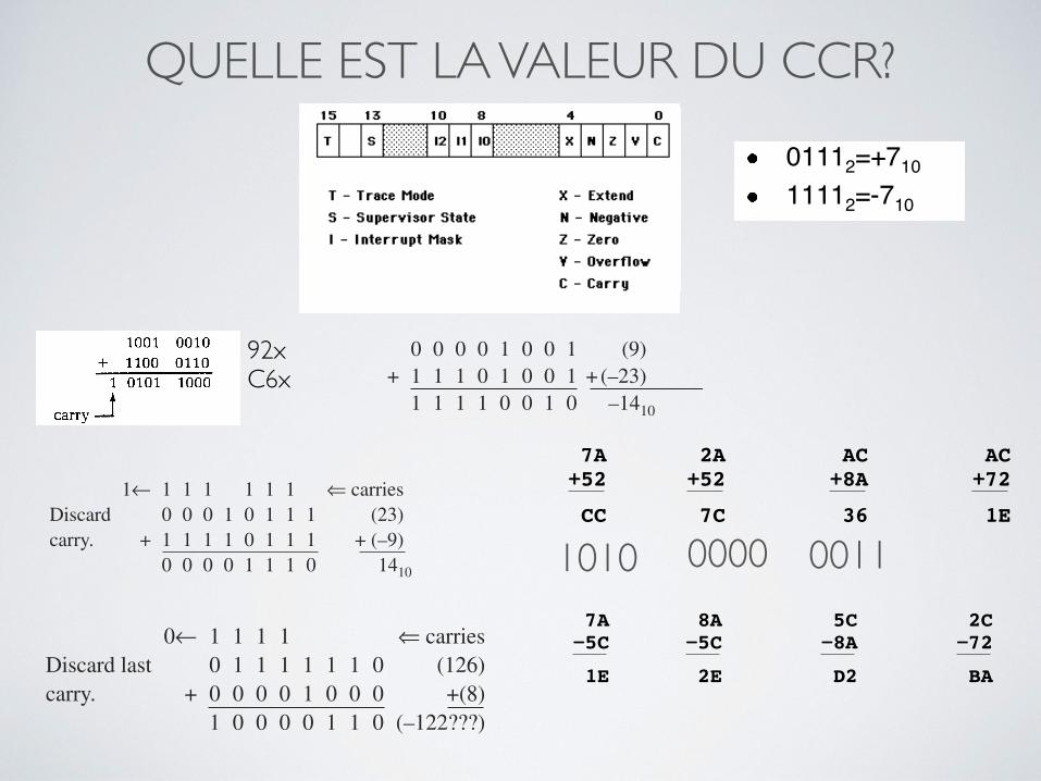
QUELLE EST LA VALEUR DU CCR?
Microprocessor-based System DesignRicardo Gutierrez-OsunaWright State University
5
Status/Condition Code Register
More significant byte: SROnly modifiable in supervisor modeDetails in later sections
Least significant byte: CCRFor user-level programsBehavior depends on instruction
Bit MeaningT Tracing for run-time
debuggingS Supervisor or
User ModeI System responds to interrupts
with a level higher than IC Set if a carry or borrow is
generated. Cleared otherwiseV Set if a signed overflow
occurs. Cleared otherwiseZ Set if the result is zero.
Cleared otherwiseN Set if the result is negative.
Cleared otherwiseX Retains information from the carry
bit for multi-precision arithmetic
92xC6x
Microprocessor-based System DesignRicardo Gutierrez-OsunaWright State University
8
2’s complement (review)How to express negative numbers in binary?
Sign-Magnitude:Use the Most Significant Bit to encode the sign
01112=+71011112=-710
2s Complement:The most commonly used form
Subtraction is made very easy (perform the operation 5-7)The range of numbers that can be represented is from -2n-1 to +2n-1-1
Binary number (+510) 0 0 0 0 0 1 0 1↓ ↓ ↓ ↓ ↓ ↓ ↓ ↓
1s complement 1 1 1 1 1 0 1 0Add 1 + 1
2s complement (-510) 1 1 1 1 1 0 1 1
2.4 / Signed Integer Representation 53
It is left as an exercise for you to verify that 111100102 is actually !1410 usingtwo’s complement notation.
EXAMPLE 2.21 Find the sum of 2310 and !910 in binary using two’s comple-ment arithmetic.
1← 1 1 1 1 1 1 ⇐ carriesDiscard 0 0 0 1 0 1 1 1 (23)carry. + 1 1 1 1 0 1 1 1 + (–9)
0 0 0 0 1 1 1 0 1410
Notice that the discarded carry in Example 2.21 did not cause an erroneous result.An overflow occurs if two positive numbers are added and the result is negative,or if two negative numbers are added and the result is positive. It is not possibleto have overflow when using two’s complement notation if a positive and a nega-tive number are being added together.
Simple computer circuits can easily detect an overflow condition using a rulethat is easy to remember. You’ll notice in Example 2.21 that the carry going intothe sign bit (a 1 is carried from the previous bit position into the sign bit position)is the same as the carry going out of the sign bit (a 1 is carried out and discarded).When these carries are equal, no overflow occurs. When they differ, an overflowindicator is set in the arithmetic logic unit, indicating the result is incorrect.
A Simple Rule for Detecting an Overflow Condition: If the carry intothe sign bit equals the carry out of the bit, no overflow has occurred. Ifthe carry into the sign bit is different from the carry out of the sign bit,overflow (and thus an error) has occurred.
The hard part is getting programmers (or compilers) to consistently check for theoverflow condition. Example 2.22 indicates overflow because the carry into the signbit (a 1 is carried in) is not equal to the carry out of the sign bit (a 0 is carried out).
EXAMPLE 2.22 Find the sum of 12610 and 810 in binary using two’s comple-ment arithmetic.
0← 1 1 1 1 ⇐ carriesDiscard last 0 1 1 1 1 1 1 0 (126)carry. + 0 0 0 0 1 0 0 0 +(8)
1 0 0 0 0 1 1 0 (–122???)
2.4 / Signed Integer Representation 53
It is left as an exercise for you to verify that 111100102 is actually !1410 usingtwo’s complement notation.
EXAMPLE 2.21 Find the sum of 2310 and !910 in binary using two’s comple-ment arithmetic.
1← 1 1 1 1 1 1 ⇐ carriesDiscard 0 0 0 1 0 1 1 1 (23)carry. + 1 1 1 1 0 1 1 1 + (–9)
0 0 0 0 1 1 1 0 1410
Notice that the discarded carry in Example 2.21 did not cause an erroneous result.An overflow occurs if two positive numbers are added and the result is negative,or if two negative numbers are added and the result is positive. It is not possibleto have overflow when using two’s complement notation if a positive and a nega-tive number are being added together.
Simple computer circuits can easily detect an overflow condition using a rulethat is easy to remember. You’ll notice in Example 2.21 that the carry going intothe sign bit (a 1 is carried from the previous bit position into the sign bit position)is the same as the carry going out of the sign bit (a 1 is carried out and discarded).When these carries are equal, no overflow occurs. When they differ, an overflowindicator is set in the arithmetic logic unit, indicating the result is incorrect.
A Simple Rule for Detecting an Overflow Condition: If the carry intothe sign bit equals the carry out of the bit, no overflow has occurred. Ifthe carry into the sign bit is different from the carry out of the sign bit,overflow (and thus an error) has occurred.
The hard part is getting programmers (or compilers) to consistently check for theoverflow condition. Example 2.22 indicates overflow because the carry into the signbit (a 1 is carried in) is not equal to the carry out of the sign bit (a 0 is carried out).
EXAMPLE 2.22 Find the sum of 12610 and 810 in binary using two’s comple-ment arithmetic.
0← 1 1 1 1 ⇐ carriesDiscard last 0 1 1 1 1 1 1 0 (126)carry. + 0 0 0 0 1 0 0 0 +(8)
1 0 0 0 0 1 1 0 (–122???)
52 Chapter 2 / Data Representation in Computer Systems
as well. Since the subtrahend (the number we complement and add) is incre-mented at the outset, however, there is no end carry-around to worry about. Wesimply discard any carries involving the high-order bits. Remember, only negativenumbers need to be converted to two’s complement notation, as indicated inExample 2.19.
EXAMPLE 2.19 Express 2310, !2310, and !910 in 8-bit binary two’s comple-ment form.
2310 = + (000101112) = 000101112!2310 = ! (000101112) = 111010002 + 1 = 111010012
!910 = ! (000010012) = 111101102 + 1 = 111101112
Suppose we are given the binary representation for a number and want to knowits decimal equivalent? Positive numbers are easy. For example, to convert thetwo’s complement value of 000101112 to decimal, we simply convert this binarynumber to a decimal number to get 23. However, converting two’s complementnegative numbers requires a reverse procedure similar to the conversion fromdecimal to binary. Suppose we are given the two’s complement binary value of111101112, and we want to know the decimal equivalent. We know this is a nega-tive number but must remember it is represented using two’s complement. Wefirst flip the bits and then add 1 (find the one’s complement and add 1). Thisresults in the following: 000010002 + 1 = 000010012. This is equivalent to thedecimal value 9. However, the original number we started with was negative, sowe end up with !9 as the decimal equivalent to 111101112.
The following two examples illustrate how to perform addition (and hencesubtraction, because we subtract a number by adding its opposite) using two’scomplement notation.
EXAMPLE 2.20 Add 910 to !2310 using two’s complement arithmetic.
0 0 0 0 1 0 0 1 (9)+ 1 1 1 0 1 0 0 1 +(–23)
1 1 1 1 0 0 1 0 –1410
EE 308 Spring 2002
Addition of hexadecimal numbers
ADDITION:
C bit set when result does not fit in word
V bit set when P + P = N N + N = P
7A+52 CC
+52 2A
7C+8A AC
36+72 AC
1E
N bit set when MSB of result is 1
Z bit set when result is 0
C: 0 C: 1
V: 0
C: 0
V: 1
C: 1
V: 1 V: 0
N: 1 N: 0 N: 1
Z: 0 Z: 0 Z: 0
N: 0
Z: 0
2
EE 308 Spring 2002
Subtraction of hexadecimal numbers
SUBTRACTION:
C bit set on borrow (when the magnitude of the subtrahend
V bit set when N − P = P P − N = N
is greater than the minuend)
7A−5C 1E
−5C 8A
2E
5C−8A D2
2C−72 BA
C: 0
V: 0
C: 1
V: 0
C: 0
V: 1V: 1
C: 1
N: 0 N: 0 N: 1 N: 1
Z: 0Z: 0Z: 0Z: 0
N bit set when MSB is 1Z bit set when result is 0
3
1010 0000 0011
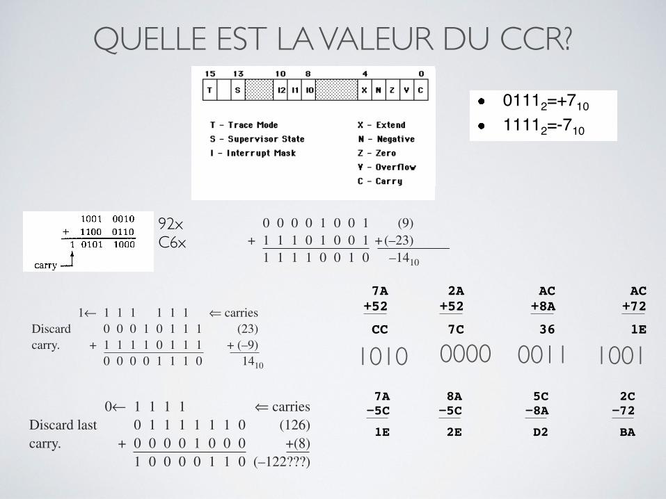
QUELLE EST LA VALEUR DU CCR?
Microprocessor-based System DesignRicardo Gutierrez-OsunaWright State University
5
Status/Condition Code Register
More significant byte: SROnly modifiable in supervisor modeDetails in later sections
Least significant byte: CCRFor user-level programsBehavior depends on instruction
Bit MeaningT Tracing for run-time
debuggingS Supervisor or
User ModeI System responds to interrupts
with a level higher than IC Set if a carry or borrow is
generated. Cleared otherwiseV Set if a signed overflow
occurs. Cleared otherwiseZ Set if the result is zero.
Cleared otherwiseN Set if the result is negative.
Cleared otherwiseX Retains information from the carry
bit for multi-precision arithmetic
92xC6x
Microprocessor-based System DesignRicardo Gutierrez-OsunaWright State University
8
2’s complement (review)How to express negative numbers in binary?
Sign-Magnitude:Use the Most Significant Bit to encode the sign
01112=+71011112=-710
2s Complement:The most commonly used form
Subtraction is made very easy (perform the operation 5-7)The range of numbers that can be represented is from -2n-1 to +2n-1-1
Binary number (+510) 0 0 0 0 0 1 0 1↓ ↓ ↓ ↓ ↓ ↓ ↓ ↓
1s complement 1 1 1 1 1 0 1 0Add 1 + 1
2s complement (-510) 1 1 1 1 1 0 1 1
2.4 / Signed Integer Representation 53
It is left as an exercise for you to verify that 111100102 is actually !1410 usingtwo’s complement notation.
EXAMPLE 2.21 Find the sum of 2310 and !910 in binary using two’s comple-ment arithmetic.
1← 1 1 1 1 1 1 ⇐ carriesDiscard 0 0 0 1 0 1 1 1 (23)carry. + 1 1 1 1 0 1 1 1 + (–9)
0 0 0 0 1 1 1 0 1410
Notice that the discarded carry in Example 2.21 did not cause an erroneous result.An overflow occurs if two positive numbers are added and the result is negative,or if two negative numbers are added and the result is positive. It is not possibleto have overflow when using two’s complement notation if a positive and a nega-tive number are being added together.
Simple computer circuits can easily detect an overflow condition using a rulethat is easy to remember. You’ll notice in Example 2.21 that the carry going intothe sign bit (a 1 is carried from the previous bit position into the sign bit position)is the same as the carry going out of the sign bit (a 1 is carried out and discarded).When these carries are equal, no overflow occurs. When they differ, an overflowindicator is set in the arithmetic logic unit, indicating the result is incorrect.
A Simple Rule for Detecting an Overflow Condition: If the carry intothe sign bit equals the carry out of the bit, no overflow has occurred. Ifthe carry into the sign bit is different from the carry out of the sign bit,overflow (and thus an error) has occurred.
The hard part is getting programmers (or compilers) to consistently check for theoverflow condition. Example 2.22 indicates overflow because the carry into the signbit (a 1 is carried in) is not equal to the carry out of the sign bit (a 0 is carried out).
EXAMPLE 2.22 Find the sum of 12610 and 810 in binary using two’s comple-ment arithmetic.
0← 1 1 1 1 ⇐ carriesDiscard last 0 1 1 1 1 1 1 0 (126)carry. + 0 0 0 0 1 0 0 0 +(8)
1 0 0 0 0 1 1 0 (–122???)
2.4 / Signed Integer Representation 53
It is left as an exercise for you to verify that 111100102 is actually !1410 usingtwo’s complement notation.
EXAMPLE 2.21 Find the sum of 2310 and !910 in binary using two’s comple-ment arithmetic.
1← 1 1 1 1 1 1 ⇐ carriesDiscard 0 0 0 1 0 1 1 1 (23)carry. + 1 1 1 1 0 1 1 1 + (–9)
0 0 0 0 1 1 1 0 1410
Notice that the discarded carry in Example 2.21 did not cause an erroneous result.An overflow occurs if two positive numbers are added and the result is negative,or if two negative numbers are added and the result is positive. It is not possibleto have overflow when using two’s complement notation if a positive and a nega-tive number are being added together.
Simple computer circuits can easily detect an overflow condition using a rulethat is easy to remember. You’ll notice in Example 2.21 that the carry going intothe sign bit (a 1 is carried from the previous bit position into the sign bit position)is the same as the carry going out of the sign bit (a 1 is carried out and discarded).When these carries are equal, no overflow occurs. When they differ, an overflowindicator is set in the arithmetic logic unit, indicating the result is incorrect.
A Simple Rule for Detecting an Overflow Condition: If the carry intothe sign bit equals the carry out of the bit, no overflow has occurred. Ifthe carry into the sign bit is different from the carry out of the sign bit,overflow (and thus an error) has occurred.
The hard part is getting programmers (or compilers) to consistently check for theoverflow condition. Example 2.22 indicates overflow because the carry into the signbit (a 1 is carried in) is not equal to the carry out of the sign bit (a 0 is carried out).
EXAMPLE 2.22 Find the sum of 12610 and 810 in binary using two’s comple-ment arithmetic.
0← 1 1 1 1 ⇐ carriesDiscard last 0 1 1 1 1 1 1 0 (126)carry. + 0 0 0 0 1 0 0 0 +(8)
1 0 0 0 0 1 1 0 (–122???)
52 Chapter 2 / Data Representation in Computer Systems
as well. Since the subtrahend (the number we complement and add) is incre-mented at the outset, however, there is no end carry-around to worry about. Wesimply discard any carries involving the high-order bits. Remember, only negativenumbers need to be converted to two’s complement notation, as indicated inExample 2.19.
EXAMPLE 2.19 Express 2310, !2310, and !910 in 8-bit binary two’s comple-ment form.
2310 = + (000101112) = 000101112!2310 = ! (000101112) = 111010002 + 1 = 111010012
!910 = ! (000010012) = 111101102 + 1 = 111101112
Suppose we are given the binary representation for a number and want to knowits decimal equivalent? Positive numbers are easy. For example, to convert thetwo’s complement value of 000101112 to decimal, we simply convert this binarynumber to a decimal number to get 23. However, converting two’s complementnegative numbers requires a reverse procedure similar to the conversion fromdecimal to binary. Suppose we are given the two’s complement binary value of111101112, and we want to know the decimal equivalent. We know this is a nega-tive number but must remember it is represented using two’s complement. Wefirst flip the bits and then add 1 (find the one’s complement and add 1). Thisresults in the following: 000010002 + 1 = 000010012. This is equivalent to thedecimal value 9. However, the original number we started with was negative, sowe end up with !9 as the decimal equivalent to 111101112.
The following two examples illustrate how to perform addition (and hencesubtraction, because we subtract a number by adding its opposite) using two’scomplement notation.
EXAMPLE 2.20 Add 910 to !2310 using two’s complement arithmetic.
0 0 0 0 1 0 0 1 (9)+ 1 1 1 0 1 0 0 1 +(–23)
1 1 1 1 0 0 1 0 –1410
EE 308 Spring 2002
Addition of hexadecimal numbers
ADDITION:
C bit set when result does not fit in word
V bit set when P + P = N N + N = P
7A+52 CC
+52 2A
7C+8A AC
36+72 AC
1E
N bit set when MSB of result is 1
Z bit set when result is 0
C: 0 C: 1
V: 0
C: 0
V: 1
C: 1
V: 1 V: 0
N: 1 N: 0 N: 1
Z: 0 Z: 0 Z: 0
N: 0
Z: 0
2
EE 308 Spring 2002
Subtraction of hexadecimal numbers
SUBTRACTION:
C bit set on borrow (when the magnitude of the subtrahend
V bit set when N − P = P P − N = N
is greater than the minuend)
7A−5C 1E
−5C 8A
2E
5C−8A D2
2C−72 BA
C: 0
V: 0
C: 1
V: 0
C: 0
V: 1V: 1
C: 1
N: 0 N: 0 N: 1 N: 1
Z: 0Z: 0Z: 0Z: 0
N bit set when MSB is 1Z bit set when result is 0
3
1010 0000 0011 1001
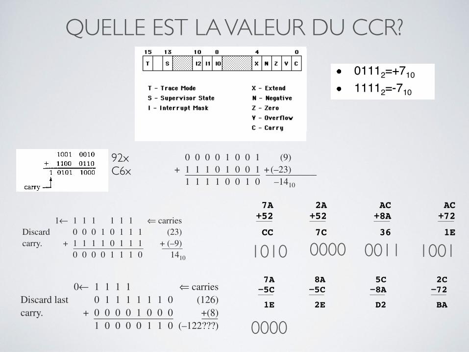
0000
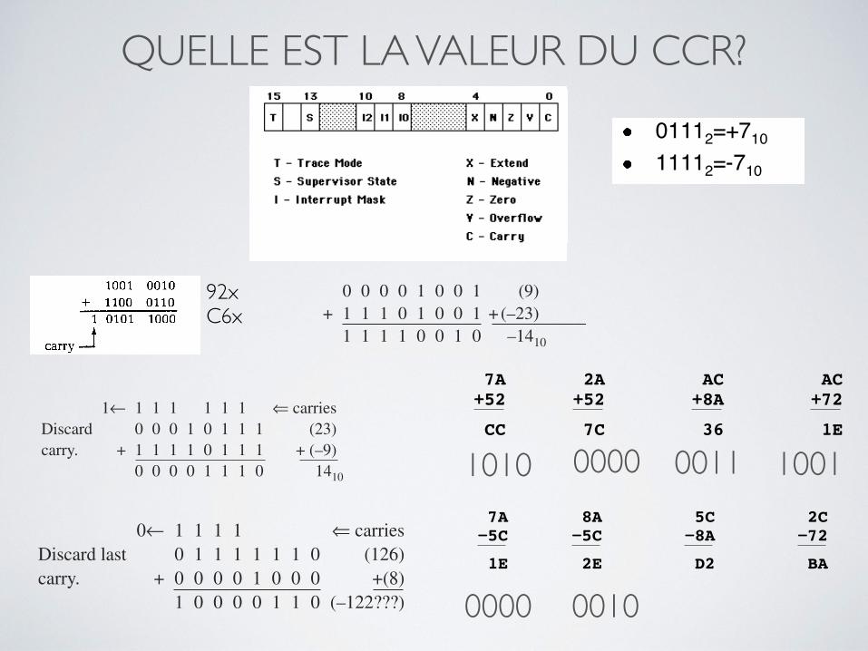
QUELLE EST LA VALEUR DU CCR?
Microprocessor-based System DesignRicardo Gutierrez-OsunaWright State University
5
Status/Condition Code Register
More significant byte: SROnly modifiable in supervisor modeDetails in later sections
Least significant byte: CCRFor user-level programsBehavior depends on instruction
Bit MeaningT Tracing for run-time
debuggingS Supervisor or
User ModeI System responds to interrupts
with a level higher than IC Set if a carry or borrow is
generated. Cleared otherwiseV Set if a signed overflow
occurs. Cleared otherwiseZ Set if the result is zero.
Cleared otherwiseN Set if the result is negative.
Cleared otherwiseX Retains information from the carry
bit for multi-precision arithmetic
92xC6x
Microprocessor-based System DesignRicardo Gutierrez-OsunaWright State University
8
2’s complement (review)How to express negative numbers in binary?
Sign-Magnitude:Use the Most Significant Bit to encode the sign
01112=+71011112=-710
2s Complement:The most commonly used form
Subtraction is made very easy (perform the operation 5-7)The range of numbers that can be represented is from -2n-1 to +2n-1-1
Binary number (+510) 0 0 0 0 0 1 0 1↓ ↓ ↓ ↓ ↓ ↓ ↓ ↓
1s complement 1 1 1 1 1 0 1 0Add 1 + 1
2s complement (-510) 1 1 1 1 1 0 1 1
2.4 / Signed Integer Representation 53
It is left as an exercise for you to verify that 111100102 is actually !1410 usingtwo’s complement notation.
EXAMPLE 2.21 Find the sum of 2310 and !910 in binary using two’s comple-ment arithmetic.
1← 1 1 1 1 1 1 ⇐ carriesDiscard 0 0 0 1 0 1 1 1 (23)carry. + 1 1 1 1 0 1 1 1 + (–9)
0 0 0 0 1 1 1 0 1410
Notice that the discarded carry in Example 2.21 did not cause an erroneous result.An overflow occurs if two positive numbers are added and the result is negative,or if two negative numbers are added and the result is positive. It is not possibleto have overflow when using two’s complement notation if a positive and a nega-tive number are being added together.
Simple computer circuits can easily detect an overflow condition using a rulethat is easy to remember. You’ll notice in Example 2.21 that the carry going intothe sign bit (a 1 is carried from the previous bit position into the sign bit position)is the same as the carry going out of the sign bit (a 1 is carried out and discarded).When these carries are equal, no overflow occurs. When they differ, an overflowindicator is set in the arithmetic logic unit, indicating the result is incorrect.
A Simple Rule for Detecting an Overflow Condition: If the carry intothe sign bit equals the carry out of the bit, no overflow has occurred. Ifthe carry into the sign bit is different from the carry out of the sign bit,overflow (and thus an error) has occurred.
The hard part is getting programmers (or compilers) to consistently check for theoverflow condition. Example 2.22 indicates overflow because the carry into the signbit (a 1 is carried in) is not equal to the carry out of the sign bit (a 0 is carried out).
EXAMPLE 2.22 Find the sum of 12610 and 810 in binary using two’s comple-ment arithmetic.
0← 1 1 1 1 ⇐ carriesDiscard last 0 1 1 1 1 1 1 0 (126)carry. + 0 0 0 0 1 0 0 0 +(8)
1 0 0 0 0 1 1 0 (–122???)
2.4 / Signed Integer Representation 53
It is left as an exercise for you to verify that 111100102 is actually !1410 usingtwo’s complement notation.
EXAMPLE 2.21 Find the sum of 2310 and !910 in binary using two’s comple-ment arithmetic.
1← 1 1 1 1 1 1 ⇐ carriesDiscard 0 0 0 1 0 1 1 1 (23)carry. + 1 1 1 1 0 1 1 1 + (–9)
0 0 0 0 1 1 1 0 1410
Notice that the discarded carry in Example 2.21 did not cause an erroneous result.An overflow occurs if two positive numbers are added and the result is negative,or if two negative numbers are added and the result is positive. It is not possibleto have overflow when using two’s complement notation if a positive and a nega-tive number are being added together.
Simple computer circuits can easily detect an overflow condition using a rulethat is easy to remember. You’ll notice in Example 2.21 that the carry going intothe sign bit (a 1 is carried from the previous bit position into the sign bit position)is the same as the carry going out of the sign bit (a 1 is carried out and discarded).When these carries are equal, no overflow occurs. When they differ, an overflowindicator is set in the arithmetic logic unit, indicating the result is incorrect.
A Simple Rule for Detecting an Overflow Condition: If the carry intothe sign bit equals the carry out of the bit, no overflow has occurred. Ifthe carry into the sign bit is different from the carry out of the sign bit,overflow (and thus an error) has occurred.
The hard part is getting programmers (or compilers) to consistently check for theoverflow condition. Example 2.22 indicates overflow because the carry into the signbit (a 1 is carried in) is not equal to the carry out of the sign bit (a 0 is carried out).
EXAMPLE 2.22 Find the sum of 12610 and 810 in binary using two’s comple-ment arithmetic.
0← 1 1 1 1 ⇐ carriesDiscard last 0 1 1 1 1 1 1 0 (126)carry. + 0 0 0 0 1 0 0 0 +(8)
1 0 0 0 0 1 1 0 (–122???)
52 Chapter 2 / Data Representation in Computer Systems
as well. Since the subtrahend (the number we complement and add) is incre-mented at the outset, however, there is no end carry-around to worry about. Wesimply discard any carries involving the high-order bits. Remember, only negativenumbers need to be converted to two’s complement notation, as indicated inExample 2.19.
EXAMPLE 2.19 Express 2310, !2310, and !910 in 8-bit binary two’s comple-ment form.
2310 = + (000101112) = 000101112!2310 = ! (000101112) = 111010002 + 1 = 111010012
!910 = ! (000010012) = 111101102 + 1 = 111101112
Suppose we are given the binary representation for a number and want to knowits decimal equivalent? Positive numbers are easy. For example, to convert thetwo’s complement value of 000101112 to decimal, we simply convert this binarynumber to a decimal number to get 23. However, converting two’s complementnegative numbers requires a reverse procedure similar to the conversion fromdecimal to binary. Suppose we are given the two’s complement binary value of111101112, and we want to know the decimal equivalent. We know this is a nega-tive number but must remember it is represented using two’s complement. Wefirst flip the bits and then add 1 (find the one’s complement and add 1). Thisresults in the following: 000010002 + 1 = 000010012. This is equivalent to thedecimal value 9. However, the original number we started with was negative, sowe end up with !9 as the decimal equivalent to 111101112.
The following two examples illustrate how to perform addition (and hencesubtraction, because we subtract a number by adding its opposite) using two’scomplement notation.
EXAMPLE 2.20 Add 910 to !2310 using two’s complement arithmetic.
0 0 0 0 1 0 0 1 (9)+ 1 1 1 0 1 0 0 1 +(–23)
1 1 1 1 0 0 1 0 –1410
EE 308 Spring 2002
Addition of hexadecimal numbers
ADDITION:
C bit set when result does not fit in word
V bit set when P + P = N N + N = P
7A+52 CC
+52 2A
7C+8A AC
36+72 AC
1E
N bit set when MSB of result is 1
Z bit set when result is 0
C: 0 C: 1
V: 0
C: 0
V: 1
C: 1
V: 1 V: 0
N: 1 N: 0 N: 1
Z: 0 Z: 0 Z: 0
N: 0
Z: 0
2
EE 308 Spring 2002
Subtraction of hexadecimal numbers
SUBTRACTION:
C bit set on borrow (when the magnitude of the subtrahend
V bit set when N − P = P P − N = N
is greater than the minuend)
7A−5C 1E
−5C 8A
2E
5C−8A D2
2C−72 BA
C: 0
V: 0
C: 1
V: 0
C: 0
V: 1V: 1
C: 1
N: 0 N: 0 N: 1 N: 1
Z: 0Z: 0Z: 0Z: 0
N bit set when MSB is 1Z bit set when result is 0
3
1010 0000 0011 1001
0000 0010
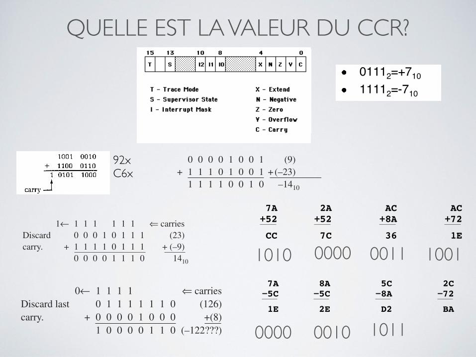
QUELLE EST LA VALEUR DU CCR?
Microprocessor-based System DesignRicardo Gutierrez-OsunaWright State University
5
Status/Condition Code Register
More significant byte: SROnly modifiable in supervisor modeDetails in later sections
Least significant byte: CCRFor user-level programsBehavior depends on instruction
Bit MeaningT Tracing for run-time
debuggingS Supervisor or
User ModeI System responds to interrupts
with a level higher than IC Set if a carry or borrow is
generated. Cleared otherwiseV Set if a signed overflow
occurs. Cleared otherwiseZ Set if the result is zero.
Cleared otherwiseN Set if the result is negative.
Cleared otherwiseX Retains information from the carry
bit for multi-precision arithmetic
92xC6x
Microprocessor-based System DesignRicardo Gutierrez-OsunaWright State University
8
2’s complement (review)How to express negative numbers in binary?
Sign-Magnitude:Use the Most Significant Bit to encode the sign
01112=+71011112=-710
2s Complement:The most commonly used form
Subtraction is made very easy (perform the operation 5-7)The range of numbers that can be represented is from -2n-1 to +2n-1-1
Binary number (+510) 0 0 0 0 0 1 0 1↓ ↓ ↓ ↓ ↓ ↓ ↓ ↓
1s complement 1 1 1 1 1 0 1 0Add 1 + 1
2s complement (-510) 1 1 1 1 1 0 1 1
2.4 / Signed Integer Representation 53
It is left as an exercise for you to verify that 111100102 is actually !1410 usingtwo’s complement notation.
EXAMPLE 2.21 Find the sum of 2310 and !910 in binary using two’s comple-ment arithmetic.
1← 1 1 1 1 1 1 ⇐ carriesDiscard 0 0 0 1 0 1 1 1 (23)carry. + 1 1 1 1 0 1 1 1 + (–9)
0 0 0 0 1 1 1 0 1410
Notice that the discarded carry in Example 2.21 did not cause an erroneous result.An overflow occurs if two positive numbers are added and the result is negative,or if two negative numbers are added and the result is positive. It is not possibleto have overflow when using two’s complement notation if a positive and a nega-tive number are being added together.
Simple computer circuits can easily detect an overflow condition using a rulethat is easy to remember. You’ll notice in Example 2.21 that the carry going intothe sign bit (a 1 is carried from the previous bit position into the sign bit position)is the same as the carry going out of the sign bit (a 1 is carried out and discarded).When these carries are equal, no overflow occurs. When they differ, an overflowindicator is set in the arithmetic logic unit, indicating the result is incorrect.
A Simple Rule for Detecting an Overflow Condition: If the carry intothe sign bit equals the carry out of the bit, no overflow has occurred. Ifthe carry into the sign bit is different from the carry out of the sign bit,overflow (and thus an error) has occurred.
The hard part is getting programmers (or compilers) to consistently check for theoverflow condition. Example 2.22 indicates overflow because the carry into the signbit (a 1 is carried in) is not equal to the carry out of the sign bit (a 0 is carried out).
EXAMPLE 2.22 Find the sum of 12610 and 810 in binary using two’s comple-ment arithmetic.
0← 1 1 1 1 ⇐ carriesDiscard last 0 1 1 1 1 1 1 0 (126)carry. + 0 0 0 0 1 0 0 0 +(8)
1 0 0 0 0 1 1 0 (–122???)
2.4 / Signed Integer Representation 53
It is left as an exercise for you to verify that 111100102 is actually !1410 usingtwo’s complement notation.
EXAMPLE 2.21 Find the sum of 2310 and !910 in binary using two’s comple-ment arithmetic.
1← 1 1 1 1 1 1 ⇐ carriesDiscard 0 0 0 1 0 1 1 1 (23)carry. + 1 1 1 1 0 1 1 1 + (–9)
0 0 0 0 1 1 1 0 1410
Notice that the discarded carry in Example 2.21 did not cause an erroneous result.An overflow occurs if two positive numbers are added and the result is negative,or if two negative numbers are added and the result is positive. It is not possibleto have overflow when using two’s complement notation if a positive and a nega-tive number are being added together.
Simple computer circuits can easily detect an overflow condition using a rulethat is easy to remember. You’ll notice in Example 2.21 that the carry going intothe sign bit (a 1 is carried from the previous bit position into the sign bit position)is the same as the carry going out of the sign bit (a 1 is carried out and discarded).When these carries are equal, no overflow occurs. When they differ, an overflowindicator is set in the arithmetic logic unit, indicating the result is incorrect.
A Simple Rule for Detecting an Overflow Condition: If the carry intothe sign bit equals the carry out of the bit, no overflow has occurred. Ifthe carry into the sign bit is different from the carry out of the sign bit,overflow (and thus an error) has occurred.
The hard part is getting programmers (or compilers) to consistently check for theoverflow condition. Example 2.22 indicates overflow because the carry into the signbit (a 1 is carried in) is not equal to the carry out of the sign bit (a 0 is carried out).
EXAMPLE 2.22 Find the sum of 12610 and 810 in binary using two’s comple-ment arithmetic.
0← 1 1 1 1 ⇐ carriesDiscard last 0 1 1 1 1 1 1 0 (126)carry. + 0 0 0 0 1 0 0 0 +(8)
1 0 0 0 0 1 1 0 (–122???)
52 Chapter 2 / Data Representation in Computer Systems
as well. Since the subtrahend (the number we complement and add) is incre-mented at the outset, however, there is no end carry-around to worry about. Wesimply discard any carries involving the high-order bits. Remember, only negativenumbers need to be converted to two’s complement notation, as indicated inExample 2.19.
EXAMPLE 2.19 Express 2310, !2310, and !910 in 8-bit binary two’s comple-ment form.
2310 = + (000101112) = 000101112!2310 = ! (000101112) = 111010002 + 1 = 111010012
!910 = ! (000010012) = 111101102 + 1 = 111101112
Suppose we are given the binary representation for a number and want to knowits decimal equivalent? Positive numbers are easy. For example, to convert thetwo’s complement value of 000101112 to decimal, we simply convert this binarynumber to a decimal number to get 23. However, converting two’s complementnegative numbers requires a reverse procedure similar to the conversion fromdecimal to binary. Suppose we are given the two’s complement binary value of111101112, and we want to know the decimal equivalent. We know this is a nega-tive number but must remember it is represented using two’s complement. Wefirst flip the bits and then add 1 (find the one’s complement and add 1). Thisresults in the following: 000010002 + 1 = 000010012. This is equivalent to thedecimal value 9. However, the original number we started with was negative, sowe end up with !9 as the decimal equivalent to 111101112.
The following two examples illustrate how to perform addition (and hencesubtraction, because we subtract a number by adding its opposite) using two’scomplement notation.
EXAMPLE 2.20 Add 910 to !2310 using two’s complement arithmetic.
0 0 0 0 1 0 0 1 (9)+ 1 1 1 0 1 0 0 1 +(–23)
1 1 1 1 0 0 1 0 –1410
EE 308 Spring 2002
Addition of hexadecimal numbers
ADDITION:
C bit set when result does not fit in word
V bit set when P + P = N N + N = P
7A+52 CC
+52 2A
7C+8A AC
36+72 AC
1E
N bit set when MSB of result is 1
Z bit set when result is 0
C: 0 C: 1
V: 0
C: 0
V: 1
C: 1
V: 1 V: 0
N: 1 N: 0 N: 1
Z: 0 Z: 0 Z: 0
N: 0
Z: 0
2
EE 308 Spring 2002
Subtraction of hexadecimal numbers
SUBTRACTION:
C bit set on borrow (when the magnitude of the subtrahend
V bit set when N − P = P P − N = N
is greater than the minuend)
7A−5C 1E
−5C 8A
2E
5C−8A D2
2C−72 BA
C: 0
V: 0
C: 1
V: 0
C: 0
V: 1V: 1
C: 1
N: 0 N: 0 N: 1 N: 1
Z: 0Z: 0Z: 0Z: 0
N bit set when MSB is 1Z bit set when result is 0
3
1010 0000 0011 1001
0000 0010 1011
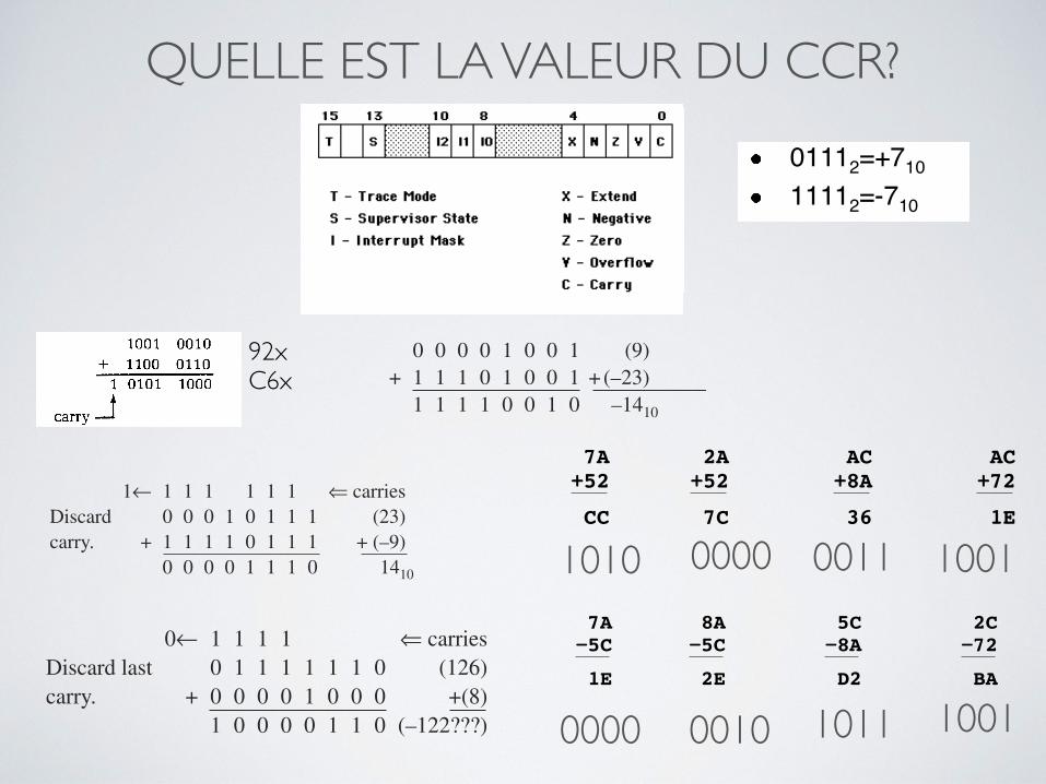
QUELLE EST LA VALEUR DU CCR?
Microprocessor-based System DesignRicardo Gutierrez-OsunaWright State University
5
Status/Condition Code Register
More significant byte: SROnly modifiable in supervisor modeDetails in later sections
Least significant byte: CCRFor user-level programsBehavior depends on instruction
Bit MeaningT Tracing for run-time
debuggingS Supervisor or
User ModeI System responds to interrupts
with a level higher than IC Set if a carry or borrow is
generated. Cleared otherwiseV Set if a signed overflow
occurs. Cleared otherwiseZ Set if the result is zero.
Cleared otherwiseN Set if the result is negative.
Cleared otherwiseX Retains information from the carry
bit for multi-precision arithmetic
92xC6x
Microprocessor-based System DesignRicardo Gutierrez-OsunaWright State University
8
2’s complement (review)How to express negative numbers in binary?
Sign-Magnitude:Use the Most Significant Bit to encode the sign
01112=+71011112=-710
2s Complement:The most commonly used form
Subtraction is made very easy (perform the operation 5-7)The range of numbers that can be represented is from -2n-1 to +2n-1-1
Binary number (+510) 0 0 0 0 0 1 0 1↓ ↓ ↓ ↓ ↓ ↓ ↓ ↓
1s complement 1 1 1 1 1 0 1 0Add 1 + 1
2s complement (-510) 1 1 1 1 1 0 1 1
2.4 / Signed Integer Representation 53
It is left as an exercise for you to verify that 111100102 is actually !1410 usingtwo’s complement notation.
EXAMPLE 2.21 Find the sum of 2310 and !910 in binary using two’s comple-ment arithmetic.
1← 1 1 1 1 1 1 ⇐ carriesDiscard 0 0 0 1 0 1 1 1 (23)carry. + 1 1 1 1 0 1 1 1 + (–9)
0 0 0 0 1 1 1 0 1410
Notice that the discarded carry in Example 2.21 did not cause an erroneous result.An overflow occurs if two positive numbers are added and the result is negative,or if two negative numbers are added and the result is positive. It is not possibleto have overflow when using two’s complement notation if a positive and a nega-tive number are being added together.
Simple computer circuits can easily detect an overflow condition using a rulethat is easy to remember. You’ll notice in Example 2.21 that the carry going intothe sign bit (a 1 is carried from the previous bit position into the sign bit position)is the same as the carry going out of the sign bit (a 1 is carried out and discarded).When these carries are equal, no overflow occurs. When they differ, an overflowindicator is set in the arithmetic logic unit, indicating the result is incorrect.
A Simple Rule for Detecting an Overflow Condition: If the carry intothe sign bit equals the carry out of the bit, no overflow has occurred. Ifthe carry into the sign bit is different from the carry out of the sign bit,overflow (and thus an error) has occurred.
The hard part is getting programmers (or compilers) to consistently check for theoverflow condition. Example 2.22 indicates overflow because the carry into the signbit (a 1 is carried in) is not equal to the carry out of the sign bit (a 0 is carried out).
EXAMPLE 2.22 Find the sum of 12610 and 810 in binary using two’s comple-ment arithmetic.
0← 1 1 1 1 ⇐ carriesDiscard last 0 1 1 1 1 1 1 0 (126)carry. + 0 0 0 0 1 0 0 0 +(8)
1 0 0 0 0 1 1 0 (–122???)
2.4 / Signed Integer Representation 53
It is left as an exercise for you to verify that 111100102 is actually !1410 usingtwo’s complement notation.
EXAMPLE 2.21 Find the sum of 2310 and !910 in binary using two’s comple-ment arithmetic.
1← 1 1 1 1 1 1 ⇐ carriesDiscard 0 0 0 1 0 1 1 1 (23)carry. + 1 1 1 1 0 1 1 1 + (–9)
0 0 0 0 1 1 1 0 1410
Notice that the discarded carry in Example 2.21 did not cause an erroneous result.An overflow occurs if two positive numbers are added and the result is negative,or if two negative numbers are added and the result is positive. It is not possibleto have overflow when using two’s complement notation if a positive and a nega-tive number are being added together.
Simple computer circuits can easily detect an overflow condition using a rulethat is easy to remember. You’ll notice in Example 2.21 that the carry going intothe sign bit (a 1 is carried from the previous bit position into the sign bit position)is the same as the carry going out of the sign bit (a 1 is carried out and discarded).When these carries are equal, no overflow occurs. When they differ, an overflowindicator is set in the arithmetic logic unit, indicating the result is incorrect.
A Simple Rule for Detecting an Overflow Condition: If the carry intothe sign bit equals the carry out of the bit, no overflow has occurred. Ifthe carry into the sign bit is different from the carry out of the sign bit,overflow (and thus an error) has occurred.
The hard part is getting programmers (or compilers) to consistently check for theoverflow condition. Example 2.22 indicates overflow because the carry into the signbit (a 1 is carried in) is not equal to the carry out of the sign bit (a 0 is carried out).
EXAMPLE 2.22 Find the sum of 12610 and 810 in binary using two’s comple-ment arithmetic.
0← 1 1 1 1 ⇐ carriesDiscard last 0 1 1 1 1 1 1 0 (126)carry. + 0 0 0 0 1 0 0 0 +(8)
1 0 0 0 0 1 1 0 (–122???)
52 Chapter 2 / Data Representation in Computer Systems
as well. Since the subtrahend (the number we complement and add) is incre-mented at the outset, however, there is no end carry-around to worry about. Wesimply discard any carries involving the high-order bits. Remember, only negativenumbers need to be converted to two’s complement notation, as indicated inExample 2.19.
EXAMPLE 2.19 Express 2310, !2310, and !910 in 8-bit binary two’s comple-ment form.
2310 = + (000101112) = 000101112!2310 = ! (000101112) = 111010002 + 1 = 111010012
!910 = ! (000010012) = 111101102 + 1 = 111101112
Suppose we are given the binary representation for a number and want to knowits decimal equivalent? Positive numbers are easy. For example, to convert thetwo’s complement value of 000101112 to decimal, we simply convert this binarynumber to a decimal number to get 23. However, converting two’s complementnegative numbers requires a reverse procedure similar to the conversion fromdecimal to binary. Suppose we are given the two’s complement binary value of111101112, and we want to know the decimal equivalent. We know this is a nega-tive number but must remember it is represented using two’s complement. Wefirst flip the bits and then add 1 (find the one’s complement and add 1). Thisresults in the following: 000010002 + 1 = 000010012. This is equivalent to thedecimal value 9. However, the original number we started with was negative, sowe end up with !9 as the decimal equivalent to 111101112.
The following two examples illustrate how to perform addition (and hencesubtraction, because we subtract a number by adding its opposite) using two’scomplement notation.
EXAMPLE 2.20 Add 910 to !2310 using two’s complement arithmetic.
0 0 0 0 1 0 0 1 (9)+ 1 1 1 0 1 0 0 1 +(–23)
1 1 1 1 0 0 1 0 –1410
EE 308 Spring 2002
Addition of hexadecimal numbers
ADDITION:
C bit set when result does not fit in word
V bit set when P + P = N N + N = P
7A+52 CC
+52 2A
7C+8A AC
36+72 AC
1E
N bit set when MSB of result is 1
Z bit set when result is 0
C: 0 C: 1
V: 0
C: 0
V: 1
C: 1
V: 1 V: 0
N: 1 N: 0 N: 1
Z: 0 Z: 0 Z: 0
N: 0
Z: 0
2
EE 308 Spring 2002
Subtraction of hexadecimal numbers
SUBTRACTION:
C bit set on borrow (when the magnitude of the subtrahend
V bit set when N − P = P P − N = N
is greater than the minuend)
7A−5C 1E
−5C 8A
2E
5C−8A D2
2C−72 BA
C: 0
V: 0
C: 1
V: 0
C: 0
V: 1V: 1
C: 1
N: 0 N: 0 N: 1 N: 1
Z: 0Z: 0Z: 0Z: 0
N bit set when MSB is 1Z bit set when result is 0
3
1010 0000 0011 1001
0000 0010 1011 1001

REGISTRES GÉNÉRAUX
• Ce ne sont pas des registres puissants (tel qu’un accumulateur) puisqu'ils n'ont pas de liaison directe avec la sortie de l'U.A.L.
• Ces registres peuvent néanmoins affecter le Registre d'Etat
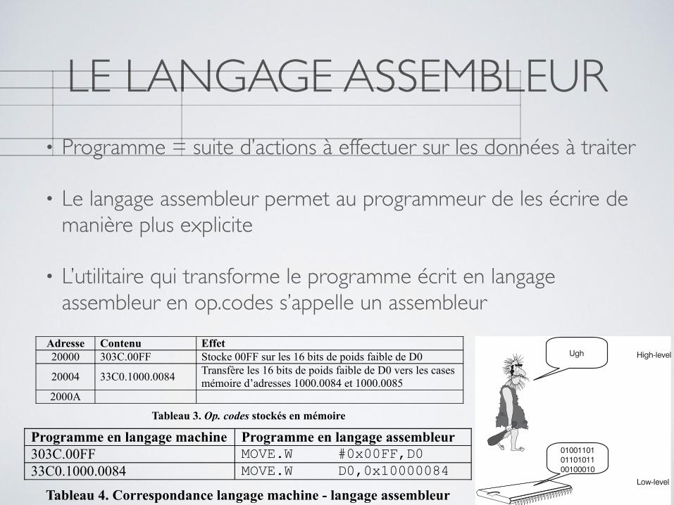
LE LANGAGE ASSEMBLEUR• Programme = suite d’actions à effectuer sur les données à traiter
• Le langage assembleur permet au programmeur de les écrire de manière plus explicite
• L’utilitaire qui transforme le programme écrit en langage assembleur en op.codes s’appelle un assembleur
Qu’est-ce que le langage assembleur ?
Un programme constitue la suite des actions à effectuer sur les données à traiter. Au bas
niveau qui nous intéresse ici, il peut être donc vu comme la suite d’instructions en langage machine rangées en mémoire de programme.
Considérons un programme qui affecte les 16 bits de poids faible de D0 avec la valeur 00FF
puis qui transfère les 16 bits de poids faible de D0 aux adresses 1000.0084 et 1000.0085.
Supposons que le stockage des instructions commence à l’adresse 20000. On trouve dans le
Tableau 3 ci-dessous les op. codes à stocker en mémoire de programme pour implanter ce
programme. (Il peut être utile de représenter l’état du système après chaque instruction.)
Adresse Contenu Effet20000 303C.00FF Stocke 00FF sur les 16 bits de poids faible de D0
20004 33C0.1000.0084Transfère les 16 bits de poids faible de D0 vers les cases
mémoire d’adresses 1000.0084 et 1000.0085
2000A
Tableau 3. Op. codes stockés en mémoire
On peut remarquer les incrémentations des adresses de la mémoire en fonction de la longueur
des instructions (2 puis 3 words).
Noter que dans un tel programme, bus d’adresses / bus de données servent à désigner /
véhiculer aussi bien du programme (lors de chaque fetch) que de la donnée (affectation des
cases d’adresse 1000.0084 et 1000.0085 par le contenu de D0). Pas en même temps bien sûr !
Cela est du à l’architecture von Neumann.
On constate tout de suite qu’un programme en langage machine est peu lisible, difficile à
mettre au point et à maintenir. Par exemple, l’utilisation de D1 à la place de D0 lors de la
première instruction aurait été codé 323C.00FF, une logique pas forcément claire sans la
documentation, et donc peu maintenable et source d’erreurs. C’est ici qu’intervient le langage assembleur. Celui-ci est un langage de programmation peu évolué. Il suit une par une les
instructions en langage machine mais il permet au programmeur de les écrire de manière plus
explicite. Ainsi les deux instructions s’écriraient dans ce langage selon le Tableau 4.
Programme en langage machine Programme en langage assembleur303C.00FF MOVE.W #0x00FF,D0
33C0.1000.0084 MOVE.W D0,0x10000084
Tableau 4. Correspondance langage machine - langage assembleur
Le gain en lisibilité est évident. La première colonne (MOVE.W pour la première ligne) est
celle des mnémoniques, la seconde (#0x00FF,D0 pour la première ligne) celle des
opérandes. On verra par la suite que la lisibilité peut être encore améliorée en désignant une
case mémoire (contenant de la donnée ou du programme) non par son adresse mais par un
identificateur (label, en français : étiquette) au nom évocateur. Ainsi, on pourra facilement
faire référence à une donnée mais aussi à un endroit précis du programme.
L’utilitaire (faisant partie des outils de développement) qui transforme le programme écrit en
langage assembleur en op. codes (instructions en langages machine) s’appelle un assembleur.
IUT1 de Grenoble – Dpt GEII2 – I2 – Introduction aux systèmes d’informatique industrielle 16
Programming – using machine code and assembly
easy understanding. There is nothing about 11000110 whichreminds us of its meaning ‘add the following number to the numberstored in the accumulator’ so a program would need to belaboriously decoded byte by byte.
Typing in streams of ones and zeros is so boring that we will makemany mistakes, particularly when we remember that a real programmay be ten thousand times longer than this. Can you imagine typingin half a million bits, finding the program does not run correctly andthen settling down to look for the mistakes?
Another problem is that the programmer must be aware of theinternal structure of the microprocessor. How else could you knowwhich register to use, or even which registers exist? So you masterall this and then change to another microprocessor and thenwhat? The whole learning process has to start again – newinstructions, new registers, and new coding requirements. It’s all toohorrible.
The difficulties with machine code hardly mattered in the early daysof the microprocessor. Everyone who programmed them werefanatics and loved the complexity and there were few serious jobsfor the microprocessor to do. This first program language was calleda ‘low-level’ language to differentiate it from our own verbalcommunication language which was called a high-level language.Machine code was later referred to as the ‘First generation’ language(see Figure 9.4).
Very soon, the microprocessor was used for an increasing range oftasks and revolutionary ideas like ‘speed and ease’ crept into the
125
Figure 9.4
High- and low-levellanguages
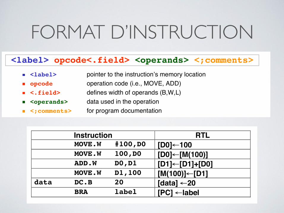
FORMAT D’INSTRUCTION
Microprocessor-based System DesignRicardo Gutierrez-OsunaWright State University
11
MC68000 instructionsInstruction format is
<label> pointer to the instruction’s memory locationopcode operation code (i.e., MOVE, ADD)<.field> defines width of operands (B,W,L)<operands> data used in the operation<;comments> for program documentation
Examples
<label> opcode<.field> <operands> <;comments>
Instruction RTL MOVE.W #100,D0 [D0]←100 MOVE.W 100,D0 [D0]←[M(100)] ADD.W D0,D1 [D1]←[D1]+[D0] MOVE.W D1,100 [M(100)]←[D1]data DC.B 20 [data] ←20 BRA label [PC] ←label
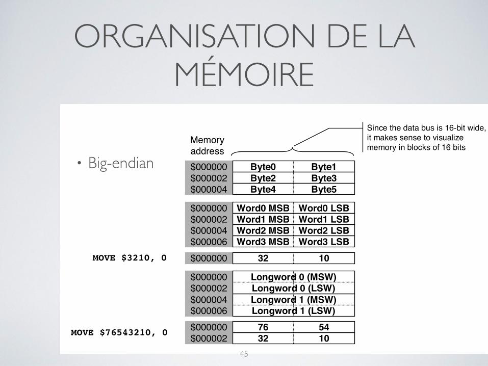
ORGANISATION DE LA MÉMOIRE
Microprocessor-based System DesignRicardo Gutierrez-OsunaWright State University
20
Memory organization example
$000000 Byte0 Byte1$000002 Byte2 Byte3$000004 Byte4 Byte5
Memoryaddress
$000000 Word0 MSB Word0 LSB$000002 Word1 MSB Word1 LSB$000004 Word2 MSB Word2 LSB$000006 Word3 MSB Word3 LSB$000000 32 10MOVE $3210, 0
$000000 Longword 0 (MSW)$000002 Longword 0 (LSW)$000004 Longword 1 (MSW)$000006 Longword 1 (LSW)$000000 76 54$000002 32 10MOVE $76543210, 0
Since the data bus is 16-bit wide, it makes sense to visualize memory in blocks of 16 bits
• Big-endian
45