
ESD Protection for Multiple Gate Field Effect Devices and ...
289
KATHOLIEKE UNIVERSITEIT LEUVEN FACULTEIT INGENIEURSWETENSCHAPPEN DEPARTEMENT ELEKTROTECHNIEK AFDELING ESAT - DIVISIE INSYS Kasteelpark Arenberg 10, B-3001 Leuven, Belgi¨ e ESD Protection for Multiple Gate Field Effect Devices and for RF CMOS Circuits Promotor : Prof. Dr. Ir. Guido GROESENEKEN Proefschrift voorgedragen tot het behalen van het doctoraat in de Ingenieurswetenschappen door Steven THIJS September 2009 In samenwerking met VZW Interuniversitair Micro-Elektronica Centrum Kapeldreef 75 B-3001 Leuven (Belgi¨ e)
Transcript of ESD Protection for Multiple Gate Field Effect Devices and ...
KATHOLIEKE UNIVERSITEIT LEUVENFACULTEIT INGENIEURSWETENSCHAPPENDEPARTEMENT ELEKTROTECHNIEKAFDELING ESAT - DIVISIE INSYSKasteelpark Arenberg 10, B-3001 Leuven, Belgie
ESD Protection forMultiple Gate Field Effect Devices
and for RF CMOS Circuits
Promotor :Prof. Dr. Ir.Guido GROESENEKEN
Proefschrift voorgedragen tothet behalen van het doctoraatin de Ingenieurswetenschappen
door
Steven THIJS
September 2009
In samenwerking met
VZW
Interuniversitair Micro-Elektronica CentrumKapeldreef 75B-3001 Leuven (Belgie)

KATHOLIEKE UNIVERSITEIT LEUVENFACULTEIT INGENIEURSWETENSCHAPPENDEPARTEMENT ELEKTROTECHNIEKAFDELING ESAT - DIVISIE INSYSKasteelpark Arenberg 10, B-3001 Leuven, Belgie
ESD Protection forMultiple Gate Field Effect Devices
and for RF CMOS Circuits
Examencommissie :Prof. Dr. Ir.A. Haegemans, voorzitterProf. Dr. Ir.G. Groeseneken, promotorProf. Dr. Ir. G. VandenboschProf. Dr. Ir. H. MaesProf. Dr. Ir. G. MeneghessoDr. Ir. M. JurczakDr. Ir. H. Gossner
Proefschrift voorgedragen tothet behalen van het doctoraatin de Ingenieurswetenschappen
door
Steven THIJS
September 2009
In samenwerking met
VZW
Interuniversitair Micro-Elektronica CentrumKapeldreef 75B-3001 Leuven (Belgie)

c©2009 Katholieke Universiteit Leuven - Faculteit IngenieurswetenschappenArenbergkasteel, B-3001 Heverlee (Belgie)
Alle rechten voorbehouden. Niets van deze uitgave mag worden vermenig-vuldigd en/of openbaar gemaakt door middel van druk, fotocopie, microfilm,elektronisch of op welke andere wijze ook zonder voorafgaande schriftelijketoestemming van de uitgever.
All rights reserved. No part of this publication may be reproduced in any formby print, photoprint, microfilm, or any other means without written permissionfrom the publisher.
ISBN: 978-94-6018-104-7
Wettelijke depotnummer: D/2009/7515/87

To Katarina, Nyo and Ime

Acknowledgements
Even though there’s only one author mentioned on the title page of this PhD,the work of the past three years would have never been possible without beingsurrounded by many world-class experts, each in their own field. Therefore, Iwould like to express my gratitude to everybody who helped me in achievingmy goals, not only for writing this thesis, but also for allowing me to grow inmy professional career.
First, I would like to thank Professor Guido Groeseneken for making it possiblefor me to return to IMEC to start this PhD and for his excellent work promotingmy thesis. Every time I thought I finished some part, Guido would read it andwould make some suggestions of things to change or things to add... and everytime it was a wise thing to follow these suggestions.
Secondly, I would like to acknowledge my jury for their careful review andcontributions: Prof. Dr. Ir. Guy Vandenbosch, Prof. Dr. Ir. Herman Maes,Prof. Dr. Ir. Gaudenzio Meneghesso, Dr. Ir. Harald Gossner and Dr. Ir.Malgorzata Jurczak.
Special thanks need to go out to my colleagues Dimitri Linten and MirkoScholz. They assisted me in so many ways in finishing this PhD! Even moreimportant, they always were in for a good laugh. Everyday it was a pleasureto come to work and I’m very proud of being a member of our successful ESDExpertise Center.
Also, I need to acknowledge the European FinFET ESD members, ChristianRuss, David Tremouilles and Alessio Griffoni. It just makes it so much easier,when you can work together with such experts!
The benefit of working at IMEC is that the experts are always closeby, youonly need to find their office. During this PhD work, I was able to findRita Rooyackers, Nadine Collaert, Ann De Keersgieter, Jonathan Borremans,Kuba Raczkowski, Morin Dehan, Bertrand Parvais, Piet Wambacq, SandeepSangameswaran and Abdelkarim Mercha. Thank you all for taking your timeto listen to my numerous questions and for all the joint publications!
I must also thank my former ESD colleagues who helped me taking my firststeps in the fascinating ESD world. They have made it possible that I am whereI am today. Thank you Vesselin Vassilev, Vincent De Heyn, Tom Daenen,Vaidyanathan Subramanian (Vaidy) and Natarajan Mahadeva Iyer (Raju)!Especially Raju deserves an extra word here. He has taught me many things,not only in my professional life, but also in my personal life. Sometimes it’sjust hard to believe how generous and kind people can be.
Finally I would like to thank my parents for giving me the chance to startstudying and make something of my life. Also, I would like to thank my wifeKatarina for all the support she has given me and for her patience of dealingwith me everyday. En natuurlijk ook een dikke kus van papa aan zijn tweeliefste schatjes Nyo en Ime!
Thank you all!
Steven ThijsLeuven, September 2009
vi
Abstract
This thesis addresses two main ESD challenges which lie ahead. First, FinFETtechnology has a limited available silicon volume to dissipate the ESD current.Therefore, a detailed ESD analysis on FinFET devices is required. Secondly,as technology downscaling allows RF applications operating at higher RFfrequencies and wider bandwidths, to be implemented in CMOS, adequateESD protection needs to be developed without compromising RF performance.Moreover, these enabling technologies simultaneously become more susceptileto ESD stress due to reduced gate oxide breakdown voltages and device powerhandling capabilities.
To be able to investigate these two challenges in more detail, limitations ofthe current commercially available ESD measurement equipment need to beovercome. In this thesis, three enhanced ESD characterization and analysistechniques have been developed. First, a Multi-level TLP system was developedenabling the measurement of the true holding voltage as well as the real devicephysics under ESD stress. Secondly, as gate oxides become more fragile dueto technology scaling, the transient turn-on response of the ESD protectiondevices becomes critical. This turn-on is investigated by a newly developedmethod to calibrate and analyze the TLP voltage and current waveforms. Wehave developed a fast, powerful method referred to as HBM-IV, where duringan HBM stress pulse, besides the similar quasi-static information as from TLP,also the transient turn-on information is obtained. HBM-IV on a high voltageexample shows that under HBM stress, voltage and current overshoots canoccur which cannot be reproduced by TLP pulses.
ESD analysis has been performed on ESD protection structures, implementedin SOI FinFET technology. It is found that a new normalization methodologyis needed for correct interpretation of the ESD results. Complex dependenciesof the different ESD performance parameters on both device geometry andprocess technology are found. Non-uniform failure exists for grounded gateNMOS devices at high current levels which can be improved by increasing gatelength and various ballasting techniques. Narrow fin devices have improvedcooling properties but suffer from reduced area efficiency. Well doping, selective
epitaxial growth, strain and silicide blocking can improve the ESD performance.From RF point of view, the large overhead capacitance of the narrow fin devicesdegrades the RF figure of merit with respect to the wide fin devices, makingwide fin devices the preferred choice. To be able to cope with this complex setof dependencies, a design methodology is developed which allows optimizationtowards a given ESD target while taking these dependencies into account. Assuch, efficient ESD protection can be designed in FinFET technology, achievingproduct level HBM levels.
Classical low-capacitive RF-ESD solutions become worse when RF frequen-cies increase resulting in either degraded RF or ESD performance. Further,CDM protection needs more attention due to its fast rising, high currentpulses, travelling along unknown current paths, causing voltage overshootsand turn-on of parasitic current paths. We propose inductive ESD protectionas narrowband RF-ESD solution due to its high ESD robustness, low RFimpact and large frequency scaling potential. It can be either implementedas a “plug-and-play” inductor to ground, or using an RF-ESD co-designedtransformer. CDM robustness is predicted by means of on-wafer VFTLPmeasurements, allowing identification of possible weak spots at an early designstage. High-quality inductors in combination with voltage clamping diodes canprovide very high VFTLP robustness. The future scaling possibilities of theinductor to ground approach are demonstrated in 45 nm planar and FinFETCMOS technologies, up to RF frequencies of 60 GHz. At these frequencies, lessESD signal couples into the RF circuit and due to the decreased inductanceof the inductor to ground, less voltage overshoot is present. Therefore, withincreasing frequency, the inductor to ground methodology becomes better interms of RF performance, ESD performance and area consumption, yieldingworld-record results.
Two-novel wideband RF-ESD protection solutions are proposed with thepotential of providing high ESD protection levels at very large bandwidths.First, the “T-diode”-concept uses a transformer to tune out the parasiticcapacitance of the ESD protection devices over a wide frequency band. Inputmatching is maintained from DC to 16.1 GHz, in a 90 m digital CMOStechnology. Local clamping and additional turn-off circuitry to prevent failureof parasitic current paths inside the RF core circuit, further increase the ESDrobustness level. Secondly, a novel distributed ESD concept (Center BalancedDistributed ESD) is developed, specifically for distributed amplifier circuits.A 1-110 GHz distributed amplifier in 45 nm CMOS is protected using thismethodology, yielding excellent ESD robustness.
In conclusion, ESD is not a showstopper for the introduction of FinFET tech-nology. Further, efficient ESD solutions can be implemented for narrow- andwideband RF circuits which exhibit both excellent RF and ESD performance.
viii
List of Acronyms
AD Analog-DigitalBCD Bipolar CMOS DMOS (smart power IC technology)BEOL Back End of LineBiCMOS Bipolar Complementary Metal Oxide Semiconductor
(technology)BJT Bipolar Junction TransistorBOX Buried OxideBV Breakdown VoltageBW BandWidthCCTLP Capacitively Coupled Transmission Line PulseCESL Contact Etch Stop LayerCBDESD Center Balanced - Distributed ESDCDM Charged Device ModelCNT Carbon Nano TubeCMOS Complimentary Metal Oxide Semiconductor (technology)DA Distributed AmplifierDC Direct CurrentDIBL Drain Induced Barrier LoweringDRC Design Rule CheckDTSCR Diode Triggered Silicon Controlled RectifierDUT Device Under TestEOT Equivalent Oxide ThicknessESD Electro Static DischargeESDA Electro Static Discharge AssociationEOS Electrical OverstressFDSOI Fully Depleted Silicon On InsulatorFED Field Effect DiodeFEOL Front End of LineFinFET Fin Field Effect TransistorFOM Figure of MeritggNMOS grounded-gate NMOSHARV i High Aspect Ratio ViaHBM Human Body Model
ix

HMM Human Metal ModelHV High VoltageIC Integrated CircuitIEC International Electrotechnical CommissionIMD Inter-Metal DielectricITRS International Technology Roadmap for SemiconductorsJEDEC Joint Electron Device Engineering CouncilLDD Lightly Doped DrainLNA Low Noise AmplifierLV TSCR Low Voltage Triggered Silicon Controlled RectifierM Multiplication FactorMEMS MicroElectroMechanical SystemMIM Metal Insulator MetalMM Machine ModelMOM Metal Oxide MetalMOCV D Metal-Organic Chemical Vapour DepositionMOSFET Metal Oxide Semiconductor Field Effect TransistorMTLP Multi Level Transmission Line PulseOEM Original Equipment ManufacturersOPC Optical Proximity CorrectionPA Power AmplifierPC Power ClampPDSOI Partially Depleted Silicon On InsulatorRF Radio FrequencySB Silicide BlockingSCE Short Channel EffectSCC Short Channel ControlSCR Silicon Controlled RectifierSDF Spacer Defined FinsSEG Selective Epitaxial GrowthSEM Scanning Electron MicroscopeSOI Silicon On InsulaterSTI Shallow Trench IsolationTCAD Technology Computer Aided DesigntCESL tensile Contact Etch Stop LayerTDR Time Domain ReflectometryTDT Time Domain TransmissionTEM Transmission Electron MicroscopeTIM Transient Interferometric MappingTSV Through-Silicon ViaTLP Transmission Line PulseTWA Traveling Wave AmplifierV DMOS Vertical Diffused Metal Oxide SemiconductorV FTLP Very Fast Transmission Line Pulse
x
UTB Ultra Thin BodyUWB Ultra WideBandWCDMA Wideband Code Division Multiple AccessWLAN Wireless Local Access NetworkWLP Wafer Level Packaging
xi


List of Symbols
β Common-Emitter Bipolar Current Gainβ Weibull SlopeBVCBO Common Base Breakdown VoltageBVCEO Common Emitter Breakdown VoltageBVox Oxide Breakdown VoltageCB Board CapacitanceCCDM CDM DUT CapacitanceCDUT DUT CapacitanceCESD Capacitance of ESD DeviceCHBM HBM CapacitanceCj Junction CapacitanceCMM MM CapacitanceCnarrow Capacitance of Narrow Fin DeviceCoh Overhead CapacitanceCpla Capacitance of Wide (Planar) Fin DeviceCPROB Voltage Probe CapacitanceCtot Total Device CapacitanceE(t) Dissipated Energy as function of TimefC Corner FrequencyfT Unity Current Gain Cutoff Frequencyγ Voltage Acceleration FactorGBW Gain Band Widthgds Output Conductancegm TransconductanceHfin Fin HeightId Diffusion Leakage CurrentIds Drain to Source CurrentIESD ESD CurrentIIP3 Third Order Input referred Intercept PointIm Modulated CurrentIon MOS Drive CurrentI(t) Current as function of Time
xiii

It1 Trigger CurrentIt2 Failure Currentk Coupling FactorLcont Size of Source/Drain Contact AreaLESD Inductance of ESD Protection InductorLg Gate LengthLs Series InductanceLSD Distance between Source/Drain Contact Area
and GateM Mutual InductanceM Multiplication FactorMn Electron Current Multiplication FactorMp Hole Current Multiplication Factorn Turn Ratio of transformerN Number of Finsnblocks Number of Parallel Device BlocksNF Noise Figureqe Injected Charge due to Diffusion Currentqm Charge in the Base RegionRCDM CDM Discharge ResistanceRHBM HBM Discharge ResistanceRmo Initial Bulk ResistanceRon On-ResistanceRs Series ResistanceRs Source ImpedanceRs,ESD Series Resistance of ESD DeviceRtot Total ResistanceS11 Input MatchingS12 Reverse IsolationS21 GainS22 Output MatchingSnorm Normalized Fin SpacingS Fin Spacingτ Carrier Lifetimeτ Electrical DelayTBOX Thickness Buried Oxide Layertfr Forward Recovery TimeTm Transit TimeVBD Breakdown VoltageVCDM CDM Precharge VoltageVDD Power Supply VoltageVdrop Voltage Drop during ESD
xiv

VGS Gate to Source VoltageVh Holding VoltageVHBM HBM Precharge VoltageVj Junction VoltageVM Modulated VoltageVmax Maximum Allowed VoltageVMM MM Precharge VoltageVSS Ground PotentialVT Threshold VoltageV (t) Voltage as function of TimeV t1 Trigger VoltageV t2 Failure VoltageWchan Channel WidthWeff Effective WidthWext Overlap Gate on FinsWfin Fin WidthWgen Generic WidthWintr Intrinsic WidthWlayout Total Layout WidthWnorm Normalized WidthZc Characteristic ImpedanceZESD Impedance of ESD Device
xv

Publication list
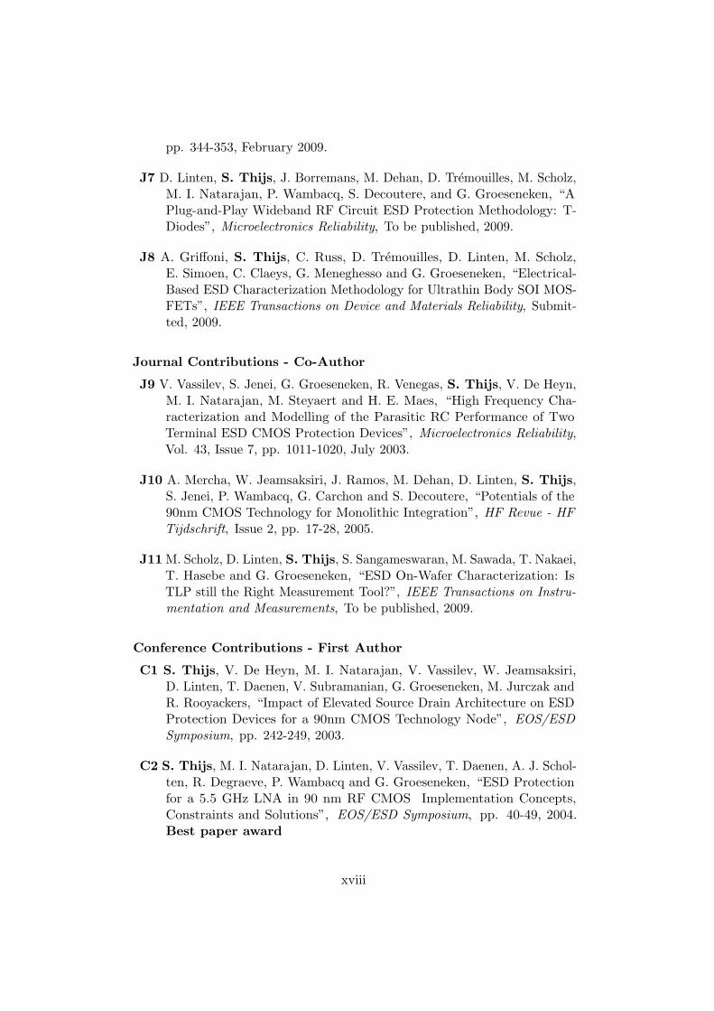
Journal Contributions - First Author
J1 S. Thijs, M. I. Natarajan, D. Linten, W. Jeamsaksiri, T. Daenen, R. De-graeve, A. J. Scholten, S. Decoutere and G. Groeseneken, “Implementa-tion of Plug-and-Play ESD Protection in 5.5 GHz 90 nm RF CMOS LNAs- Concepts, Constraints and Solutions”, Microelectronics Reliability, Vol.46, Issues 5-6, pp. 702-712, May-June 2006.
J2 S. Thijs, D. Tremouilles, C. Russ, A. Griffoni, N. Collaert, R. Rooya-ckers, D. Linten, M. Scholz, C. Duvvury, H. Gossner, M. Jurczak andG. Groeseneken, “Characterization and Optimization of Sub-32nm Fin-FET Devices for ESD Applications”, IEEE Transactions on ElectronDevices, Vol. 55, no. 12, pp. 3507-3516, December 2008.
Journal Contributions - Second Author
J3 V. Vassilev, S. Thijs, P. L. Segura, P. Wambacq, P. Leroux, M. I. Natara-jan, G. Groeseneken, H. E. Maes and M. Steyaert, “ESD RF Co-DesignMethodology for the State of the Art RF-CMOS Blocks”, Microelectro-nics Reliability, Vol. 45, Issue 2, pp. 255-268, February 2005.
J4 D. Linten, S. Thijs, M. I. Natarajan, W. Jeamsaksiri, J. Ramos, A. Mer-cha, S. Jenei, S. Donnay and S. Decoutere, “A 5-GHz Fully IntegratedESD-Protected Low-Noise Amplifier in 90-nm RF CMOS”, IEEE Journalof Solid-State Circuits, Vol. 40, Issue 7, pp. 1434-1442, July 2005.
J5 D. Tremouilles, S. Thijs, Ph. Roussel, M. I. Natarajan, V. Vassilev andG. Groeseneken, “Transient Voltage Overshoot in TLP Testing - Real orArtifact?”, Microelectronics Reliability, Vol. 47, Issue 7, pp. 1016-1024,July 2007.
J6 J. Borremans, S. Thijs, P. Wambacq, Y. Rolain, D. Linten and M. Kuijk,“A Fully-Integrated 7.3 kV HBM ESD-Protected Transformer-Based 4.5-6GHz CMOS LNA”, Journal of Solid-State Circuits, Vol. 44, Number 2,
xvii
pp. 344-353, February 2009.
J7 D. Linten, S. Thijs, J. Borremans, M. Dehan, D. Tremouilles, M. Scholz,M. I. Natarajan, P. Wambacq, S. Decoutere, and G. Groeseneken, “APlug-and-Play Wideband RF Circuit ESD Protection Methodology: T-Diodes”, Microelectronics Reliability, To be published, 2009.
J8 A. Griffoni, S. Thijs, C. Russ, D. Tremouilles, D. Linten, M. Scholz,E. Simoen, C. Claeys, G. Meneghesso and G. Groeseneken, “Electrical-Based ESD Characterization Methodology for Ultrathin Body SOI MOS-FETs”, IEEE Transactions on Device and Materials Reliability, Submit-ted, 2009.
Journal Contributions - Co-Author
J9 V. Vassilev, S. Jenei, G. Groeseneken, R. Venegas, S. Thijs, V. De Heyn,M. I. Natarajan, M. Steyaert and H. E. Maes, “High Frequency Cha-racterization and Modelling of the Parasitic RC Performance of TwoTerminal ESD CMOS Protection Devices”, Microelectronics Reliability,Vol. 43, Issue 7, pp. 1011-1020, July 2003.
J10 A. Mercha, W. Jeamsaksiri, J. Ramos, M. Dehan, D. Linten, S. Thijs,S. Jenei, P. Wambacq, G. Carchon and S. Decoutere, “Potentials of the90nm CMOS Technology for Monolithic Integration”, HF Revue - HFTijdschrift, Issue 2, pp. 17-28, 2005.
J11 M. Scholz, D. Linten, S. Thijs, S. Sangameswaran, M. Sawada, T. Nakaei,T. Hasebe and G. Groeseneken, “ESD On-Wafer Characterization: IsTLP still the Right Measurement Tool?”, IEEE Transactions on Instru-mentation and Measurements, To be published, 2009.
Conference Contributions - First Author
C1 S. Thijs, V. De Heyn, M. I. Natarajan, V. Vassilev, W. Jeamsaksiri,D. Linten, T. Daenen, V. Subramanian, G. Groeseneken, M. Jurczak andR. Rooyackers, “Impact of Elevated Source Drain Architecture on ESDProtection Devices for a 90nm CMOS Technology Node”, EOS/ESDSymposium, pp. 242-249, 2003.
C2 S. Thijs, M. I. Natarajan, D. Linten, V. Vassilev, T. Daenen, A. J. Schol-ten, R. Degraeve, P. Wambacq and G. Groeseneken, “ESD Protectionfor a 5.5 GHz LNA in 90 nm RF CMOS Implementation Concepts,Constraints and Solutions”, EOS/ESD Symposium, pp. 40-49, 2004.Best paper award
xviii
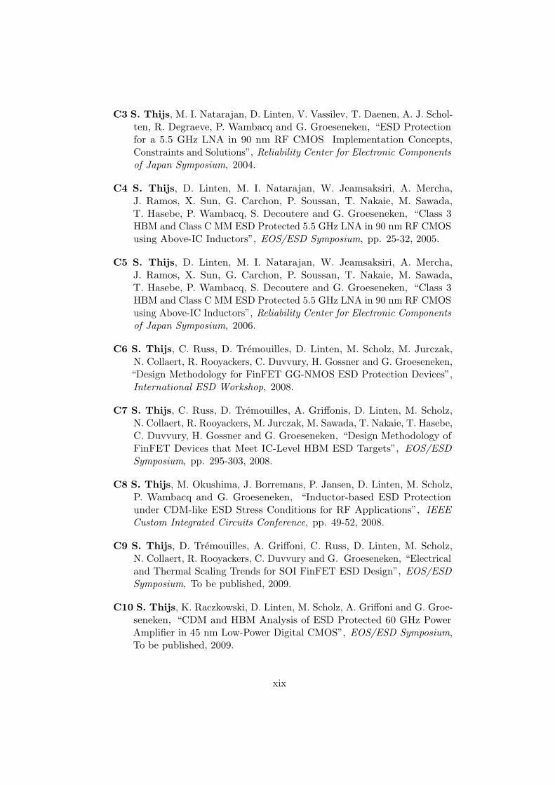
C3 S. Thijs, M. I. Natarajan, D. Linten, V. Vassilev, T. Daenen, A. J. Schol-ten, R. Degraeve, P. Wambacq and G. Groeseneken, “ESD Protectionfor a 5.5 GHz LNA in 90 nm RF CMOS Implementation Concepts,Constraints and Solutions”, Reliability Center for Electronic Componentsof Japan Symposium, 2004.
C4 S. Thijs, D. Linten, M. I. Natarajan, W. Jeamsaksiri, A. Mercha,J. Ramos, X. Sun, G. Carchon, P. Soussan, T. Nakaie, M. Sawada,T. Hasebe, P. Wambacq, S. Decoutere and G. Groeseneken, “Class 3HBM and Class C MM ESD Protected 5.5 GHz LNA in 90 nm RF CMOSusing Above-IC Inductors”, EOS/ESD Symposium, pp. 25-32, 2005.
C5 S. Thijs, D. Linten, M. I. Natarajan, W. Jeamsaksiri, A. Mercha,J. Ramos, X. Sun, G. Carchon, P. Soussan, T. Nakaie, M. Sawada,T. Hasebe, P. Wambacq, S. Decoutere and G. Groeseneken, “Class 3HBM and Class C MM ESD Protected 5.5 GHz LNA in 90 nm RF CMOSusing Above-IC Inductors”, Reliability Center for Electronic Componentsof Japan Symposium, 2006.
C6 S. Thijs, C. Russ, D. Tremouilles, D. Linten, M. Scholz, M. Jurczak,N. Collaert, R. Rooyackers, C. Duvvury, H. Gossner and G. Groeseneken,“Design Methodology for FinFET GG-NMOS ESD Protection Devices”,International ESD Workshop, 2008.
C7 S. Thijs, C. Russ, D. Tremouilles, A. Griffonis, D. Linten, M. Scholz,N. Collaert, R. Rooyackers, M. Jurczak, M. Sawada, T. Nakaie, T. Hasebe,C. Duvvury, H. Gossner and G. Groeseneken, “Design Methodology ofFinFET Devices that Meet IC-Level HBM ESD Targets”, EOS/ESDSymposium, pp. 295-303, 2008.
C8 S. Thijs, M. Okushima, J. Borremans, P. Jansen, D. Linten, M. Scholz,P. Wambacq and G. Groeseneken, “Inductor-based ESD Protectionunder CDM-like ESD Stress Conditions for RF Applications”, IEEECustom Integrated Circuits Conference, pp. 49-52, 2008.
C9 S. Thijs, D. Tremouilles, A. Griffoni, C. Russ, D. Linten, M. Scholz,N. Collaert, R. Rooyackers, C. Duvvury and G. Groeseneken, “Electricaland Thermal Scaling Trends for SOI FinFET ESD Design”, EOS/ESDSymposium, To be published, 2009.
C10 S. Thijs, K. Raczkowski, D. Linten, M. Scholz, A. Griffoni and G. Groe-seneken, “CDM and HBM Analysis of ESD Protected 60 GHz PowerAmplifier in 45 nm Low-Power Digital CMOS”, EOS/ESD Symposium,To be published, 2009.
xix
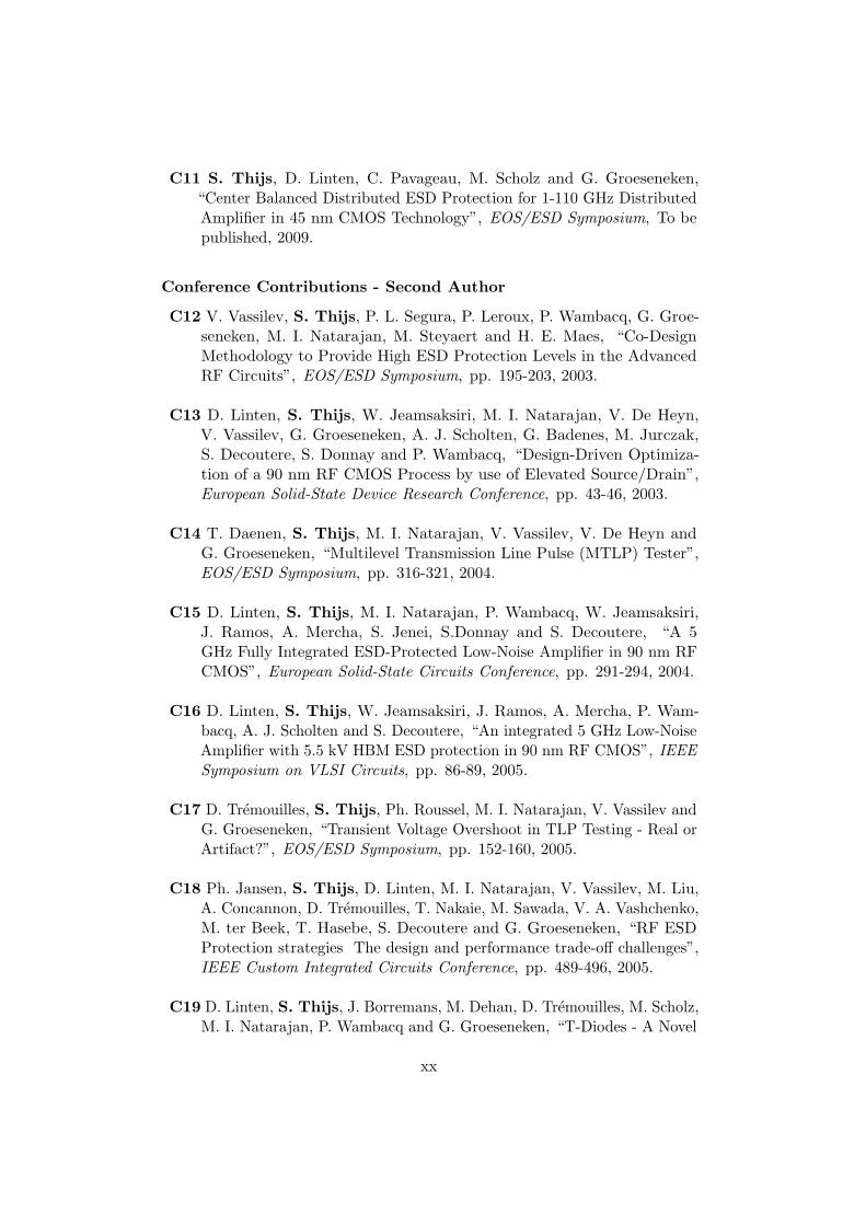
C11 S. Thijs, D. Linten, C. Pavageau, M. Scholz and G. Groeseneken,“Center Balanced Distributed ESD Protection for 1-110 GHz DistributedAmplifier in 45 nm CMOS Technology”, EOS/ESD Symposium, To bepublished, 2009.
Conference Contributions - Second Author
C12 V. Vassilev, S. Thijs, P. L. Segura, P. Leroux, P. Wambacq, G. Groe-seneken, M. I. Natarajan, M. Steyaert and H. E. Maes, “Co-DesignMethodology to Provide High ESD Protection Levels in the AdvancedRF Circuits”, EOS/ESD Symposium, pp. 195-203, 2003.
C13 D. Linten, S. Thijs, W. Jeamsaksiri, M. I. Natarajan, V. De Heyn,V. Vassilev, G. Groeseneken, A. J. Scholten, G. Badenes, M. Jurczak,S. Decoutere, S. Donnay and P. Wambacq, “Design-Driven Optimiza-tion of a 90 nm RF CMOS Process by use of Elevated Source/Drain”,European Solid-State Device Research Conference, pp. 43-46, 2003.
C14 T. Daenen, S. Thijs, M. I. Natarajan, V. Vassilev, V. De Heyn andG. Groeseneken, “Multilevel Transmission Line Pulse (MTLP) Tester”,EOS/ESD Symposium, pp. 316-321, 2004.
C15 D. Linten, S. Thijs, M. I. Natarajan, P. Wambacq, W. Jeamsaksiri,J. Ramos, A. Mercha, S. Jenei, S.Donnay and S. Decoutere, “A 5GHz Fully Integrated ESD-Protected Low-Noise Amplifier in 90 nm RFCMOS”, European Solid-State Circuits Conference, pp. 291-294, 2004.
C16 D. Linten, S. Thijs, W. Jeamsaksiri, J. Ramos, A. Mercha, P. Wam-bacq, A. J. Scholten and S. Decoutere, “An integrated 5 GHz Low-NoiseAmplifier with 5.5 kV HBM ESD protection in 90 nm RF CMOS”, IEEESymposium on VLSI Circuits, pp. 86-89, 2005.
C17 D. Tremouilles, S. Thijs, Ph. Roussel, M. I. Natarajan, V. Vassilev andG. Groeseneken, “Transient Voltage Overshoot in TLP Testing - Real orArtifact?”, EOS/ESD Symposium, pp. 152-160, 2005.
C18 Ph. Jansen, S. Thijs, D. Linten, M. I. Natarajan, V. Vassilev, M. Liu,A. Concannon, D. Tremouilles, T. Nakaie, M. Sawada, V. A. Vashchenko,M. ter Beek, T. Hasebe, S. Decoutere and G. Groeseneken, “RF ESDProtection strategies The design and performance trade-off challenges”,IEEE Custom Integrated Circuits Conference, pp. 489-496, 2005.
C19 D. Linten, S. Thijs, J. Borremans, M. Dehan, D. Tremouilles, M. Scholz,M. I. Natarajan, P. Wambacq and G. Groeseneken, “T-Diodes - A Novel
xx
Plug-and-Play Wideband RF Circuit ESD Protection Methodology”,EOS/ESD Symposium, pp. 242-249, 2007.
C20 D. Linten, S. Thijs, J. Borremans, M. Dehan, D. Tremouilles, M. Scholz,M. I. Natarajan, P. Wambacq and G. Groeseneken, “T-Diodes - A NovelPlug-and-Play Wideband RF Circuit ESD Protection Methodology”,Reliability Center for Electronic Components of Japan Symposium, 2007.
C21 D. Tremouilles, S. Thijs, C. Russ, J. Schneider, C. Duvvury, N. Col-laert, D. Linten, M. Scholz, M. Jurczak, H. Gossner and G. Groeseneken,“Understanding the Optimization of Sub-45nm FinFET Devices for ESDApplications”, EOS/ESD Symposium, pp. 408-415, 2007.
C22 J. Borremans, S. Thijs, P. Wambacq, D. Linten, Y. Rolain, andM. Kuijk, “A 5 kV HBM Transformer-Based ESD Protected 5-6 GHzLNA”, IEEE Symposium on VLSI Circuits, pp. 100-101, 2007.
C23 M. Scholz, S. Thijs, D. Linten, D. Tremouilles, M. Sawada, T. Nakaie,T. Hasebe, M. I. Natarajan and G. Groeseneken, “Calibrated Wafer-LevelHBM Measurements for Quasi-Static and Transient Device Analysis”,EOS/ESD Symposium, pp. 89-94, 2007.
C24 D. Linten, S. Thijs, M. Scholz, D. Tremouilles, M. Sawada, T. Nakaie,T. Hasebe and G. Groeseneken, “Characterization and Modeling ofDiodes in Sub-45 nm CMOS Technologies under HBM Stress Condi-tions”, EOS/ESD Symposium, pp. 158-164, 2007.
C25 M. I. Natarajan, S. Thijs, D. Tremouilles, D. Linten, J. Loo, N. Collaert,M. Sawada, T. Hasebe, M. Jurczak, S. Decoutere and G. Groeseneken,“ESD protection for sub-45 nm MugFET Technology”, 14th IEEE Inter-national Symposium on Physical and Failure Analysis, 2007.
C26 G. Groeseneken, S. Thijs, D. Linten, M. Scholz, J. Borremans, N. Col-laert and M. Jurczak, “Challenges and solutions for ESD protection inadvanced logic and RF CMOS technologies”, International ESD Work-shop, 2008.
C27 A. Griffoni, S. Thijs, C. Russ, D. Tremouilles, M. Scholz, D. Linten,N. Collaert, R. Rooyackers, C. Duvvury, H. Gossner, G. Meneghessoand G. Groeseneken, “Impact of Strain on ESD Robustness of FinFETDevices”, IEEE International Electron Device Meeting, pp. 341-344,2008.
xxi
C28 A. Griffoni, S. Thijs, C. Russ, D. Tremouilles, D. Linten, M. Scholz,N. Collaert, L. Witters, G. Meneghesso and G. Groeseneken, “Next Ge-neration FinFET Devices in Bulk Silicon Technology and Their Benefitsfor ESD Robustness”, EOS/ESD Symposium, To be published, 2009.
C29 D. Linten, S. Thijs, M. Okushima, J. Borremans, M. Scholz, M. Dehanand G. Groeseneken, “A 4.5 kV HBM, 300 V CDM ESD protected DC-to-16.1 GHz wideband LNA in 90 nm CMOS”, EOS/ESD Symposium,To be published, 2009.
C30 J. Borremans, S. Thijs, S. Decoutere and P. Wambacq, “Low-CostFeedback-Enabled LNAs in 45nm CMOS”, European Solid-State CircuitsConference, paper 3048, 2009.
C31 A. Griffoni, S. Thijs, D. Linten, M. Scholz, G. Groeseneken andG. Meneghesso, “An Insight into the Parasitic Capacitances of SOIand Bulk FinFET Devices”, European Heterostructure Technology Work-shop, To be published, 2009.
C32 A. Griffoni, S. Thijs, C. Russ, D. Tremouilles, D. Linten, M. Scholz,N. Collaert, L. Witters, G. Meneghesso and G. Groeseneken, “Next Ge-neration FinFET Devices in Bulk Silicon Technology and Their Benefitsfor ESD Robustness”, Reliability Center for Electronic Components ofJapan Symposium, To be published, 2009.
Conference Contributions - Co-Author
C33 V. Vassilev, M. Lorenzini, Ph. Jansen, V. A. Vashchenko, J. J. Yang,A. Concannon, D. Archer, G. Groeseneken, M. I. Natarajan, M. ter Beek,S. Thijs, B. J. Choi, M. Steyaert and H. E. Maes, “Snapback CircuitModel for Cascoded NMOS ESD Over-Voltage Protection Structures”,European Solid-State Device Research Conference, pp. 561-564, 2003.
C34 M. I. Natarajan, V. Vassilev, S. Thijs, V. De Heyn, T. Daenen andG. Groeseneken, “ESD Reliability Issues in Sub-Micron CMOS - Trendsand Challenges”, 2nd MRS International Conference on Materials forAdvanced Technologies & IUMRS, 2003.
C35 W. Jeamsaksiri, A. Mercha, J. Ramos, D. Linten, S. Thijs, S. Jenei,C. Detcheverry, P. Wambacq, R. Velghe and S. Decoutere, “Integrationof a 90nm RF CMOS Technology (200 GHz fmax - 150 GHz fT NMOS)Demonstrated on a 5 GHz LNA”, IEEE Symposium on VLSI Technology,pp. 100-101, 2004.
xxii
C36 V. Vassilev, M. Lorenzini, Ph. Jansen, G. Groeseneken, S. Thijs,M. I. Natarajan, M. Steyaert and H. E. Maes, “Advanced Modelingand Parameter Extraction of the MOSFET ESD Breakdown Triggeringin the 90nm CMOS Node Technologies”, EOS/ESD Symposium, pp.98-106, 2004.
C37 J. Ramos, A. Mercha, W. Jeamsaksiri, D. Linten, S. Jenei, R. Rooyackers,R. Verbeeck, S. Thijs, A. J. Scholten, P. Wambacq, I. Debusschere andS. Decoutere “90nm RF CMOS Technology for Low-Power 900 MHzApplications”, European Solid-State Device Research Conference, pp.329-332, 2004.
C38 M. I. Natarajan, V. Vassilev, S. Thijs and G. Groeseneken, “Modelingand Simulation for ESD Protection Circuit Design and Optimization”,Proceedings International Conference on Semiconductor Electronics, pp.A12-A18, 2004.
C39 D. Linten, L. Aspemeyr, W. Jeamsaksiri, J. Ramos, A. Mercha, S. Jenei,S. Thijs, R. Garcia, H. Jacobsson, P. Wambacq, S. Donnay and G. Groe-seneken, “Low-Power 5 GHz LNA and VCO in 90 nm RF CMOS”, IEEESymposium on VLSI Circuits, pp. 372-375, 2004.
C40 M. I. Natarajan, V. Vassilev, S. Thijs and G. Groeseneken, “ESDProtection Challenges in RFCMOS Circuits an Overview”, IEEE Inter-national Symposium on Microwaves, 2004.
C41 J. Ramos, W. Jeamsaksiri, A. Mercha, S. Thijs, D. Linten, P. Wambacq,B. De Jaeger, I. Debusschere, S. Biesemans and S. Decoutere “Hot-CarrierDegradation on the Analogue/RF Performances of a 90 nm RF-CMOSTechnology Demonstrated in a 900 MHz Low-Power LNA”, ProceedingsIEEE VLSI-TSA International Symposium on VLSI Technology, pp.64-65, 2005.
C42 W. Jeamsaksiri, D. Linten, S. Thijs, G. Carchon, J. Ramos, A. Mercha,X. Sun, P. Soussan, M. Dehan, T. Chiarella, R. Venegas, V. Subrama-nian, A. J. Scholten, P. Wambacq, R. Velghe, G. Mannaert, N. Heylen,R. Verbeeck, W. Boullart, I. Heyvaert, M. I. Natarajan, G. Groeseneken,I. Debusschere, S. Biesemans and S. Decoutere, “A Low-Cost 90 nm RF-CMOS Platform for Record RF Circuit Performance”, IEEE Symposiumon VLSI Technology, pp. 60-61, 2005.
C43 D. Linten, X. Sun, S. Thijs, M. I. Natarajan, A. Mercha, G. Carchon,P. Wambacq, T. Nakaie and S. Decoutere, “Low-Power Low-Noise HighlyESD Robust LNA and VCO Design Using Above IC Inductors”, IEEE
xxiii
Custom Integrated Circuits Conference, pp. 497-500, 2005.
C44 M. I. Natarajan, D. Linten, S. Thijs, Ph. Jansen, D. Tremouilles,W. Jeamsaksiri, T. Nakaie, M. Sawada, T. Hasebe, S. Decoutere andG. Groeseneken, “RFCMOS ESD Protection and Reliability”, 12th IEEEInternational Symposium on Physical and Failure Analysis, 2005.
C45 D. Linten, M. I. Natarajan, S. Thijs, S. Van Huylenbroeck, S. Xiao,G. Carchon, S. Decoutere, M. Sawada, T. Hasebe and G. Groeseneken,“Implementation of 6 kV ESD Protection for a 17 GHz LNA in 130nmSiGeC BiCMOS”, IEEE International Conference on SemiconductorElectronics, pp. A7-A12, 2006.
C46 V. A. Vashchenko, Ph. Jansen, M. Scholz, P. Hopper, M. Sawada,T. Nakaei, T. Hasebe and S. Thijs, “Voltage Overshoot Study in 20VDeMOS-SCR Devices”, EOS/ESD Symposium, pp. 53-57, 2007.
C47 P. Wambacq, A. Mercha, K. Scheir, B. Verbruggen, J. Borremans,V. De Heyn, S. Thijs, D. Linten, G. Van der Plas, B. Parvais, M. Dehan,S. Decoutere, C. Soens, N. Collaert and M. Jurczak, “Advanced PlanarBulk and Multigate CMOS Technology: Analog Circuit Benchmarkingup to mm-wave Frequencies”, IEEE International Solid-State CircuitsConference, pp. 528-533, 2008.
C48 G. Groeseneken, F. Crupi, A. Shickova, S. Thijs, D. Linten, B. Kaczer,N. Collaert, M. Jurczak, “Reliability Issues in MugFET Nanodevices”,IEEE International Reliability Physics Symposium, 2008.
C49 D. Linten, V. Vashchenko, M. Scholz, P. Jansen, D. Lafonteese, S. Thijs,M. Sawada, T. Hasebe, P. Hopper, and G. Groeseneken, “Analysis ofHigh Voltage ESD Protection Devices under HBM ESD stress”, Interna-tional ESD Workshop, 2008.
C50 S. Sangameswaran, J. De Coster, D. Linten, M. Scholz, S. Thijs,L. Haspeslagh, A. Witvrouw, C. Van Hoof, G. Groeseneken and I. DeWolf, “ESD Issues in MEMS: A case study in Micromirrors”, Interna-tional ESD Workshop, 2008.
C51 D. Linten, V. Vashchenko, M. Scholz, P. Jansen, D. Lafonteese, S. Thijs,M. Sawada, T. Hasebe, P. Hopper, and G. Groeseneken, “Extreme Vol-tage and Current Overshoots in HV Snapback Devices during HBM ESDstress”, EOS/ESD Symposium, pp. 204-210, 2008.
xxiv
C52 S. Sangameswaran, J. De Coster, D. Linten, M. Scholz, S. Thijs,L. Haspeslagh, A. Witvrouw, C. Van Hoof, G. Groeseneken and I. De Wolf,“ESD Reliability issues in Microelectromechanical Systems (MEMS): Acase study in micromirrors”, EOS/ESD Symposium, pp. 249-257, 2008.
C53 J. Borremans, B. Parvais, M. Dehan, S. Thijs, P. Wambacq, A. Mercha,M. Kuijk, G. Carchon and S. Decoutere, “Perspective of RF design infuture planar and FinFET CMOS”, IEEE Radio Frequency IntegratedCircuits Symposium, pp. 75-78, 2008.
C54 M. Scholz , D. Linten , S. Thijs, M. Sawada, T. Nakaei, T. Hasebeand G. Groeseneken, “On-wafer Human Metal Model System-level ESDStress on Component Level”, Reliability Center for Electronic Compo-nents of Japan Symposium, 2008.
C55 K. Raczkowski, S. Thijs, W. De Raedt, B. Nauwelaers and P. Wambacq,“50-67 GHz ESD Protected Power Amplifiers in Digital 45 nm LP CMOS”,International Solid-State Circuits Conference, paper 22.5, 2009.
C56 M. Scholz, D. Linten, S. Thijs, M. Sawada, T. Nakaei, T. Hasebe,D. Lafonteese, V. Vashchenko, G. Vandersteen, G. Groeseneken, “On-wafer Human Metal Model measurements for System-level ESD analysis”,EOS/ESD Symposium, To be published, 2009.
C57 D. LaFonteese, V. Vashchenko, D. Linten, M. Scholz, S. Thijs, A. Kozyrev,M. Sawada, T. Nakaei, T. Hasebe, P. Hopper and G. Groeseneken, “Self-Protection Capability of Power Arrays”, EOS/ESD Symposium, To bepublished, 2009.
C58 S. Sangameswaran, J. Coster, M. Scholz, D. Linten, S. Thijs, C. VanHoof, I. De Wolf and G. Groeseneken, “A Study of Breakdown Me-chanisms in Electrostatic Actuators using Mechanical Response underEOS-ESD Stress”, EOS/ESD Symposium, To be published, 2009.
C59 D. Linten, P. Roussel, M. Scholz, S. Thijs, A. Griffoni, M. Sawada,T. Hasebe and G. Groeseneken, “Calibration of Very Fast TLP Tran-sients”, EOS/ESD Symposium, To be published, 2009.
C60 D. Linten, P. Roussel, M. Scholz, S. Thijs, A. Griffoni, M. Sawada,T. Hasebe and G. Groeseneken, “Calibration of Very Fast TLP Tran-sients”, Reliability Center for Electronic Components of Japan Sympo-sium, To be published, 2009.
xxv
C61 M. Scholz, D. Linten, S. Thijs, M. Sawada, T. Nakaei, T. Hasebe,D. Lafonteese, V. Vashchenko, G. Vandersteen, G. Groeseneken, “On-wafer Human Metal Model measurements for System-level ESD analysis”,Reliability Center for Electronic Components of Japan Symposium, Tobe published, 2009.
Workshops and Tutorials
W1 J. Ramos, A. Mercha, W. Jeamsaksiri, D. Linten, S. Jenei, S. Thijs,A. J. Scholten, P. Wambacq, I. Debusschere and S. Decoutere, “RFCMOS Modeling for Circuit Design”, Microwave Device Modeling &Design of Microwave Systems, 2004.
W2 J. Ramos, A. Mercha, W. Jeamsaksiri, D. Linten, S. Jenei, S. Thijs,A. J. Scholten, P. Wambacq, I. Debusschere and S. Decoutere, “A90 nm RF CMOS Technology Supported by Device Modeling and CircuitDemonstrators”, MOS-AK/ESSCIRC Workshop, 2004.
T1 D. Linten, S. Thijs, M. Scholz, D. Tremouilles, M. I. Natarajan andG. Groeseneken, “Technology-Aware ESD-Reliable RF CMOS CircuitDesign”, IEEE Custom Integrated Circuits Conference Tutorial, 2006.
T2 D. Linten, S. Thijs and M. I. Natarajan, “ESD Protection for WidebandRFCMOS Circuits - Challenges, Options and Trade-offs”, IEEE RadioFrequency Integrated Circuits Symposium Tutorial, 2006.
W3 S. Thijs, “RF ESD Protection - Trends and Outlook”, ReliabilityCenter for Electronic Components of Japan Symposium Workshop, 2006.
T3 M. I. Natarajan, D. Linten, S. Thijs and G. Groeseneken, “ESD Pro-tection for Semiconductor Devices”, IEEE International Symposium onPhysical and Failure Analysis Tutorial, 2007.
W4 S. Thijs and D. Linten, “Protecting High Frequency Circuits”, EOS/ESDSymposium Workshop, 2007.
W5 D. Linten, S. Thijs and M. Scholz, “Exploring ESD Protection in Sub-32 nm CMOS Technology”, Reliability Center for Electronic Componentsof Japan Workshop, 2007.
T4 D. Linten and S. Thijs, “Advanced RF Implementation Flow Course -Electrostatic discharge (ESD) protection”, IDESA - Implementation ofWidespread IC Design Skills in Advanced deep Submicron Technologiesat European Academia, 2008-2009.
xxvi
Patents
P1 S. Thijs, N. M. Iyer, V. Vassilev, T. Daenen and V. De Heyn, “Methodof Determing Current-Voltage Characteristics of a Device”, United StatesPatent, US 7,181,352, 2004.
Patent Applications
P2 S. Thijs, N. M. Iyer, V. Vassilev, T. Daenen and V. De Heyn, “Methodof Determing Current-Voltage Characteristics of a Device”, EuropeanPatent Application, EP 1,480,046,A1, 2003.
P3 S. Thijs, N. M. Iyer and D. Linten, “Electrostatic Discharge Protected Cir-cuits”, United States Patent Application Publication, US 2007/0058308.
P4 S. Thijs and D. Tremouilles, “Fast Triggering ESD Protection Deviceand Method for Designing Same”, United States Patent ApplicationPublication, US 2009/0073621, A1.
P5 S. Thijs and D. Tremouilles, “Fast Triggering ESD Protection Deviceand Method for Designing Same”, European Patent Application, EP2037501, A1, 2007.
P6 S. Thijs, D. Tremouilles and C. Russ, “Electronic Circuit and Method ofManufacturing an Electronic Circuit”, United States Patent ApplicationPublication, US 2009/0065868, A1.
P7 S. Thijs, M. Scholz, D. Tremouilles and D. Linten, “Method for Calibra-ting an Electrostatic Discharge Tester”, United States Patent ApplicationPublication, US 0027063A1, 2009.
P8 S. Thijs, M. Scholz, D. Tremouilles and D. Linten, “Method for Calibra-ting an Electrostatic Discharge Tester”, European Patent Application,EP 1972953 A1, 2008.
P9 S. Thijs, D. Tremouilles and D. Linten, “ESD design methodologyfor ESD protection devices in FinFET technology”, European PatentApplication, EP 09159669.2, 2009.
Patent Submissions
P10 S. Thijs and D. Tremouilles, “Field Effect Diode (FED) in FinFETtechnology”
xxvii
P11 S. Thijs and D. Tremouilles, “Silicon Controlled Rectifier (SCR) inFinFET technology”
P12 S. Thijs, D. Linten and D. Tremouilles, “Bidirectional ESD powerclamp for SOI CMOS technologies (e.g. FinFET)”
P13 S. Thijs, D. Linten and D. Tremouilles, “Keep-off circuit for ESDprotection devices”
P14 S. Thijs and D. Linten, “Center Balanced Distributed ESD protection”
P15 S. Thijs and D. Linten, “Turn Off of parasitic path in core circuit”
xxviii
NederlandstaligeSamenvatting
ESD Bescherming voorMeervoudige Gate Veld Effect Structuren
en voor RF CMOS Circuits
Inleiding
Twee grote uitdagingen liggen in het verschiet voor de ESD ontwerpingenieur.Is ESD enerzijds een spelbreker voor de introductie van FinFET technologiedoor het geringe silicium volume van de structuren? Is anderzijds een goedeESD bescherming compatibel met de strenge vereisten voor RF circuits metsteeds hoger wordende RF frequenties? Voor deze laatste uitdaging zijn zoweloplossingen nodig voor smalbandige als breedbandige RF toepassingen. Ookmoet er meer aandacht besteed worden aan CDM bescherming ten opzichtevan HBM, omdat dit type ESD stress meer kritisch is en er moeilijker tegen tebeschermen valt. Om deze twee uitdagingen goed aan te kunnen gaan, moeteneerst de beperkingen van de huidige meetsystemen worden weggewerkt.
ESD Karakterisatie en Analyze Technieken
In deze thesis werden er drie nieuwe ESD karakterisatie en analyze techniekenontworpen die de bestaande technieken en meetsystemen verder uitbreiden.Eerst hebben we een Multi-Level Transmissie Lijn Puls (MTLP) meetsysteemontworpen. Vervolgens hebben we een transient analyze uitgevoerd op ESD pro-tectiestructuren door gebruik te maken van de spannings- en stroomgolfvormenverkregen tijdens een klassieke TLP meting. Als laatste hebben we een HumanBody Model-IV (HBM-IV) curve verkregen door de transient spannings- enstroomgolfvormen van een HBM meting te combineren.
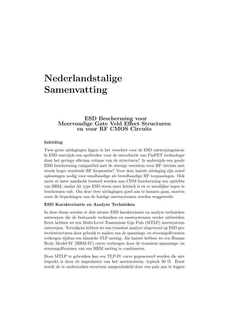
Door MTLP te gebruiken kan een TLP-IV curve gegenereerd worden die nietbeperkt is door de impedantie van het meetsysteem, typisch 50 Ω. Eerstwordt de te onderzoeken structuur aangeschakeld door een puls aan te leggen
-3
-2
-1
0
1
2
3
4
-30
-20
-10
0
10
20
30
40
0 50 100 150 200
Vol
tage
[V]
Current [m
A]
Time [ns]
measurementregion 1
measurementregion 2
Figuur 0.1: Resulterende spannings en stroom golfvormen tijdens een MTLPmeting op een open belasting.
-5
0
5
10
15
20
20 40 60 80 100 120 140 160
Without corr.With corr.
Vol
tage
[V]
Time [ns]
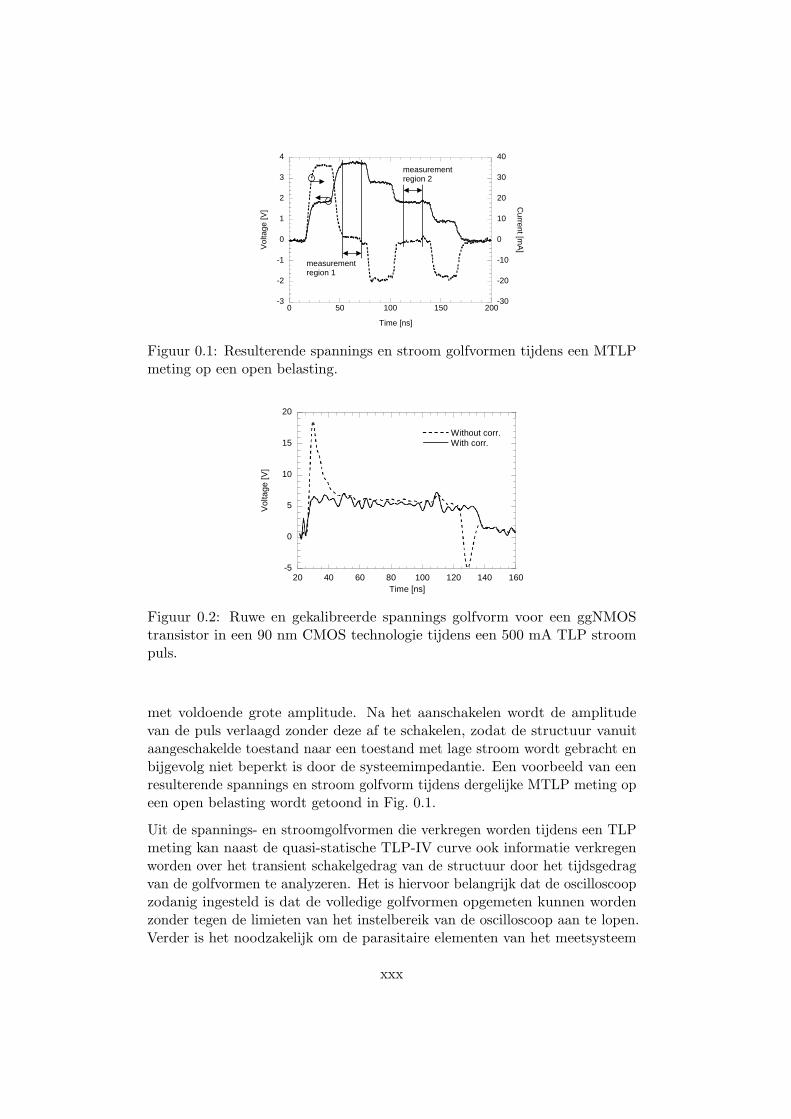
Figuur 0.2: Ruwe en gekalibreerde spannings golfvorm voor een ggNMOStransistor in een 90 nm CMOS technologie tijdens een 500 mA TLP stroompuls.
met voldoende grote amplitude. Na het aanschakelen wordt de amplitudevan de puls verlaagd zonder deze af te schakelen, zodat de structuur vanuitaangeschakelde toestand naar een toestand met lage stroom wordt gebracht enbijgevolg niet beperkt is door de systeemimpedantie. Een voorbeeld van eenresulterende spannings en stroom golfvorm tijdens dergelijke MTLP meting opeen open belasting wordt getoond in Fig. 0.1.
Uit de spannings- en stroomgolfvormen die verkregen worden tijdens een TLPmeting kan naast de quasi-statische TLP-IV curve ook informatie verkregenworden over het transient schakelgedrag van de structuur door het tijdsgedragvan de golfvormen te analyzeren. Het is hiervoor belangrijk dat de oscilloscoopzodanig ingesteld is dat de volledige golfvormen opgemeten kunnen wordenzonder tegen de limieten van het instelbereik van de oscilloscoop aan te lopen.Verder is het noodzakelijk om de parasitaire elementen van het meetsysteem
xxx
0
1
2
3
4
0 50 100 150 200
4000 V1000 V
Cur
rent
[A]
Voltage [V]
A'
B'
A
B
C TLP Vt1
C'
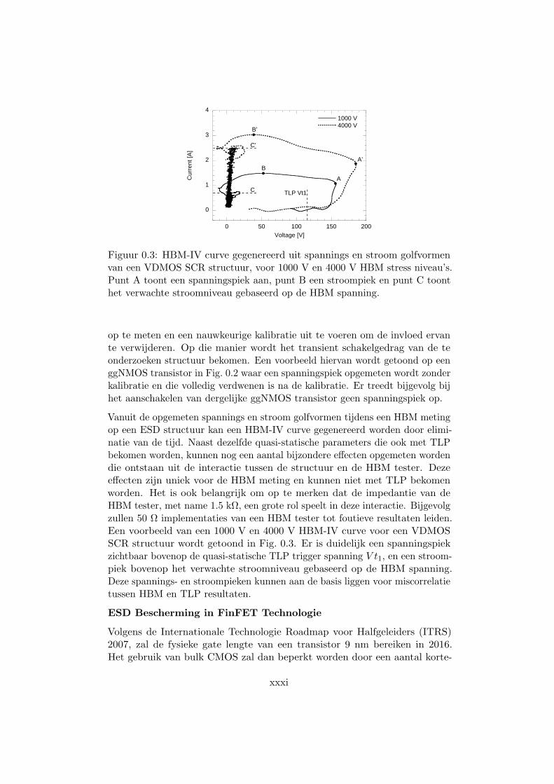
Figuur 0.3: HBM-IV curve gegenereerd uit spannings en stroom golfvormenvan een VDMOS SCR structuur, voor 1000 V en 4000 V HBM stress niveau’s.Punt A toont een spanningspiek aan, punt B een stroompiek en punt C toonthet verwachte stroomniveau gebaseerd op de HBM spanning.
op te meten en een nauwkeurige kalibratie uit te voeren om de invloed ervante verwijderen. Op die manier wordt het transient schakelgedrag van de teonderzoeken structuur bekomen. Een voorbeeld hiervan wordt getoond op eenggNMOS transistor in Fig. 0.2 waar een spanningspiek opgemeten wordt zonderkalibratie en die volledig verdwenen is na de kalibratie. Er treedt bijgevolg bijhet aanschakelen van dergelijke ggNMOS transistor geen spanningspiek op.
Vanuit de opgemeten spannings en stroom golfvormen tijdens een HBM metingop een ESD structuur kan een HBM-IV curve gegenereerd worden door elimi-natie van de tijd. Naast dezelfde quasi-statische parameters die ook met TLPbekomen worden, kunnen nog een aantal bijzondere effecten opgemeten wordendie ontstaan uit de interactie tussen de structuur en de HBM tester. Dezeeffecten zijn uniek voor de HBM meting en kunnen niet met TLP bekomenworden. Het is ook belangrijk om op te merken dat de impedantie van deHBM tester, met name 1.5 kΩ, een grote rol speelt in deze interactie. Bijgevolgzullen 50 Ω implementaties van een HBM tester tot foutieve resultaten leiden.Een voorbeeld van een 1000 V en 4000 V HBM-IV curve voor een VDMOSSCR structuur wordt getoond in Fig. 0.3. Er is duidelijk een spanningspiekzichtbaar bovenop de quasi-statische TLP trigger spanning V t1, en een stroom-piek bovenop het verwachte stroomniveau gebaseerd op de HBM spanning.Deze spannings- en stroompieken kunnen aan de basis liggen voor miscorrelatietussen HBM en TLP resultaten.
ESD Bescherming in FinFET Technologie
Volgens de Internationale Technologie Roadmap voor Halfgeleiders (ITRS)2007, zal de fysieke gate lengte van een transistor 9 nm bereiken in 2016.Het gebruik van bulk CMOS zal dan beperkt worden door een aantal korte-
xxxi
GATE
SOURCE LANDING PAD
DRAIN LANDING PAD
LG
LSD
Lcont
Wext Wfin SN = numberof fins
A
A’
BOX
SILICON
POLYSILICON
TBOX
HfinSILICON
TiNHfSiON
SOURCECONTACT
DRAINCONTACT
SiO2
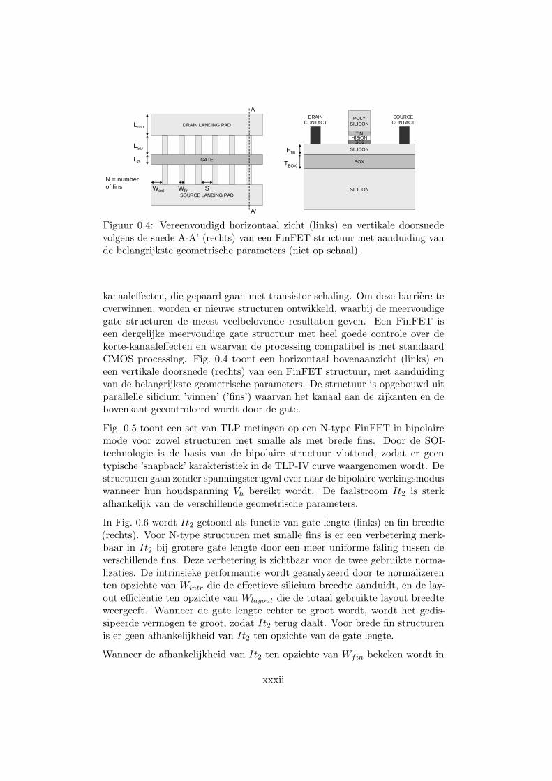
Figuur 0.4: Vereenvoudigd horizontaal zicht (links) en vertikale doorsnedevolgens de snede A-A’ (rechts) van een FinFET structuur met aanduiding vande belangrijkste geometrische parameters (niet op schaal).
kanaaleffecten, die gepaard gaan met transistor schaling. Om deze barriere teoverwinnen, worden er nieuwe structuren ontwikkeld, waarbij de meervoudigegate structuren de meest veelbelovende resultaten geven. Een FinFET iseen dergelijke meervoudige gate structuur met heel goede controle over dekorte-kanaaleffecten en waarvan de processing compatibel is met standaardCMOS processing. Fig. 0.4 toont een horizontaal bovenaanzicht (links) eneen vertikale doorsnede (rechts) van een FinFET structuur, met aanduidingvan de belangrijkste geometrische parameters. De structuur is opgebouwd uitparallelle silicium ’vinnen’ (’fins’) waarvan het kanaal aan de zijkanten en debovenkant gecontroleerd wordt door de gate.
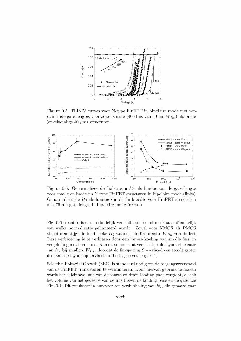
Fig. 0.5 toont een set van TLP metingen op een N-type FinFET in bipolairemode voor zowel structuren met smalle als met brede fins. Door de SOI-technologie is de basis van de bipolaire structuur vlottend, zodat er geentypische ’snapback’ karakteristiek in de TLP-IV curve waargenomen wordt. Destructuren gaan zonder spanningsterugval over naar de bipolaire werkingsmoduswanneer hun houdspanning Vh bereikt wordt. De faalstroom It2 is sterkafhankelijk van de verschillende geometrische parameters.
In Fig. 0.6 wordt It2 getoond als functie van gate lengte (links) en fin breedte(rechts). Voor N-type structuren met smalle fins is er een verbetering merk-baar in It2 bij grotere gate lengte door een meer uniforme faling tussen deverschillende fins. Deze verbetering is zichtbaar voor de twee gebruikte norma-lizaties. De intrinsieke performantie wordt geanalyzeerd door te normalizerenten opzichte van Wintr die de effectieve silicium breedte aanduidt, en de lay-out efficientie ten opzichte van Wlayout die de totaal gebruikte layout breedteweergeeft. Wanneer de gate lengte echter te groot wordt, wordt het gedis-sipeerde vermogen te groot, zodat It2 terug daalt. Voor brede fin structurenis er geen afhankelijkheid van It2 ten opzichte van de gate lengte.
Wanneer de afhankelijkheid van It2 ten opzichte van Wfin bekeken wordt in
xxxii
0
0.02
0.04
0.06
0.08
0.1
0 1 2 3 4 5
Narrow fin
Wide fin
Cur
rent
[A]
Voltage [V]
75105
155355
955
Gate Length (nm)
It2
Vh=Vt1
Ron
Figuur 0.5: TLP-IV curves voor N-type FinFET in bipolaire mode met ver-schillende gate lengtes voor zowel smalle (400 fins van 30 nm Wfin) als brede(enkelvoudige 40 µm) structuren.
0
2
4
6
8
10
0 200 400 600 800 1000
Narrow fin - norm. WintrNarrow fin - norm. WlayoutWide fin
Nor
mal
ized
failu
re c
urre
nt It
2 [m
A/u
m]
Gate length [nm]
0
1
2
3
4
5
6
7
10 100 1000 104 105
NMOS - norm. WintrNMOS - norm. WlayoutPMOS - norm. WintrPMOS - norm. Wlayout
Nor
mal
ized
failu
re c
urre
nt It
2 [m
A/u
m]
Fin width [nm]
Figuur 0.6: Genormalizeerde faalstroom It2 als functie van de gate lengtevoor smalle en brede fin N-type FinFET structuren in bipolaire mode (links).Genormalizeerde It2 als functie van de fin breedte voor FinFET structurenmet 75 nm gate lengte in bipolaire mode (rechts).
Fig. 0.6 (rechts), is er een duidelijk verschillende trend merkbaar afhankelijkvan welke normalizatie gehanteerd wordt. Zowel voor NMOS als PMOSstructuren stijgt de intrinsieke It2 wanneer de fin breedte Wfin vermindert.Deze verbetering is te verklaren door een betere koeling van smalle fins, invergelijking met brede fins. Aan de andere kant verslechtert de layout efficientievan It2 bij smallere Wfin, doordat de fin-spacing S overhead een steeds groterdeel van de layout oppervlakte in beslag neemt (Fig. 0.4).
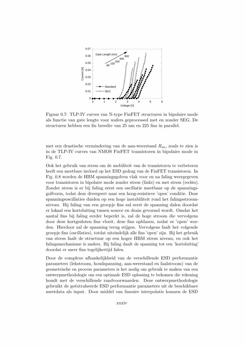
Selective Epitaxial Growth (SEG) is standaard nodig om de toegangsweerstandvan de FinFET transistoren te verminderen. Door hiervan gebruik te makenwordt het siliciumvolume van de source en drain landing pads vergroot, alsookhet volume van het gedeelte van de fins tussen de landing pads en de gate, zieFig. 0.4. Dit resulteert in ongeveer een verdubbeling van It2, die gepaard gaat
xxxiii
0
0.01
0.02
0.03
0.04
0.05
0.06
0.07
0 1 2 3 4 5 6
Standard
SEG
Cur
rent
[A]
Voltage [V]
Gate Length (nm)
80150
250400
900
Figuur 0.7: TLP-IV curves van N-type FinFET structuren in bipolaire modeals functie van gate lengte voor wafers geprocessed met en zonder SEG. Destructuren hebben een fin breedte van 25 nm en 225 fins in parallel.
met een drastische vermindering van de aan-weerstand Ron, zoals te zien isin de TLP-IV curves van NMOS FinFET transistoren in bipolaire mode inFig. 0.7.
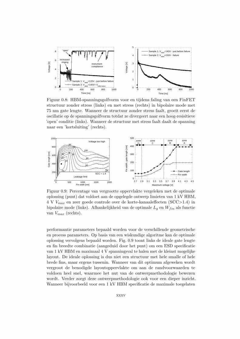
Ook het gebruik van stress om de mobiliteit van de transistoren te verbeterenheeft een meetbare invloed op het ESD gedrag van de FinFET transistoren. InFig. 0.8 worden de HBM spanningsgolven vlak voor en na faling weergegevenvoor transistoren in bipolaire mode zonder stress (links) en met stress (rechts).Zonder stress is er bij faling eerst een oscillatie meetbaar op de spannings-golfvorm, todat deze divergeert naar een hoog-resistieve ’open’ conditie. Dezespanningsoscillaties duiden op een hoge instabiliteit rond het falingsstroom-niveau. Bij faling van een groepje fins zal eerst de spanning dalen doordater lokaal een kortsluiting tussen source en drain gevormd wordt. Omdat hetaantal fins bij faling eerder beperkt is, zal de hoge stroom die vervolgensdoor deze kortgesloten fins vloeit, deze fins opblazen, zodat ze ’open’ wor-den. Hierdoor zal de spanning terug stijgen. Vervolgens faalt het volgendegroepje fins (oscillaties), totdat uiteindelijk alle fins ’open’ zijn. Bij het gebruikvan stress faalt de structuur op een hoger HBM stress niveau, en ook hetfalingsmechanisme is anders. Bij faling daalt de spanning tot een ’kortsluiting’doordat er meer fins tegelijkertijd falen.
Door de complexe afhankelijkheid van de verschillende ESD performantieparameters (lekstroom, houdspanning, aan-weerstand en faalstroom) van degeometrische en process parameters is het nodig om gebruik te maken van eenontwerpmethodologie om een optimale ESD oplossing te bekomen die rekeninghoudt met de verschillende randvoorwaarden. Deze ontwerpmethodologiegebruikt de geextraheerde ESD performantie parameters uit de beschikbaremeetdata als input. Door middel van lineaire interpolatie kunnen de ESD
xxxiv
0
2
4
6
8
0 200 400 600 800 1000
Sample 1: VHBM
=120V - just before failure
Sample 3: VHBM
=140V> VHBM,failure
Vol
tage
[V]
Time [ns]
increased ringing
instrument compliance
'open'
0
1
2
3
4
5
0 200 400 600 800 1000
Sample 1: VHBM
=140V - just before failure
Sample 2: VHBM
=150V - failure
Vol
tage
[V]
Time [ns]
Figuur 0.8: HBM-spanningsgolfvorm voor en tijdens faling van een FinFETstructuur zonder stress (links) en met stress (rechts) in bipolaire mode met75 nm gate lengte. Wanneer de structuur zonder stress faalt, groeit eerst deoscillatie op de spanningsgolfvorm totdat ze divergeert naar een hoog-resisitieve’open’ conditie (links). Wanneer de structuur met stress faalt daalt de spanningnaar een ’kortsluiting’ (rechts).
10
20
20
3040
40
50
60
70
80
90
100
Fin width [nm]
Gat
e le
ngth
[nm
]
0 500 1000 1500 20000
200
400
600
800
1000
Voltage too high
SCC = 1.4Leakage limit
0
100
200
300
400
500
2.7 2.9 3.1 3.3 3.5 3.7 3.9 4.1 4.3 4.5
Fin width
Gate lengthFin
wid
th, g
ate
leng
th [n
m]
Maximum voltage [V]
zoneD
zoneC
zoneB
zoneA
Figuur 0.9: Percentage van vergrootte oppervlakte vergeleken met de optimaleoplossing (punt) dat voldoet aan de opgelegde ontwerp limieten van 1 kV HBM,4 V Vmax en zeer goede controle over de korte-kanaaleffecten (SCC>1.4) inbipolaire mode (links). Afhankelijkheid van de optimale Lg en Wfin als functievan Vmax (rechts).
performantie parameters bepaald worden voor de verschillende geometrischeen process parameters. Op basis van een wiskundige algoritme kan de optimaleoplossing vervolgens bepaald worden. Fig. 0.9 toont links de ideale gate lengteen fin breedte combinatie (aangeduid door het punt) om een ESD specificatievan 1 kV HBM en maximaal 4 V spanningsval te halen met de kleinst mogelijkelayout. De ideale oplossing is dus niet een structuur met hele smalle of helebrede fins, maar ergens tussenin. Wanneer van dit optimum afgeweken wordtvergroot de benodigde layoutoppervlakte om aan de randvoorwaarden tevoldoen heel snel, waarmee het nut van de ontwerpmethodologie bewezenwordt. Verder zorgt deze ontwerpmethodologie ook voor een dieper inzicht.Wanneer bijvoorbeeld voor een 1 kV HBM specificatie de maximale toegelaten
xxxv
LsLg
M1M2Lload
C2RFIN RFOUTC1
ESD
2ES
D 1
ESD
3
VDD
VSSFiguur 0.10: Basis van on-chip ESD bescherming. Het circuit is een lage ruisversterker (LNA) die gebruikt wordt als demonstrator. ESD1-3 zijn de ESDbeschermingsstructuren.
spanning verminderd wordt van 4.5 tot 2.7 V, kan men in Fig. 0.9 (rechts)verschillende zones onderscheiden hoe de optimale gate lengte en fin breedtezich moeten gedragen om tot het optimum te komen.
Al deze resultaten tonen aan dat de ESD gevoeligheid van FinFET struc-turen geen spelbreker is voor de introductie van FinFETs voor geavanceerdenanotechnologieen, zolang ESD reeds beschouwd wordt tijdens de techno-logieontwikkeling. Maar zelfs met deze kennis blijft het ontwerp van ESDbescherming voor FinFET technologie een uitdaging.
ESD Bescherming voor Smalbandige RF CMOS Circuits
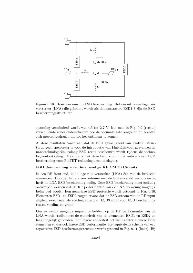
In een RF front-end, is de lage ruis versterker (LNA) een van de kritischeelementen. Doordat hij via een antenne met de buitenwereld verbonden is,heeft de LNA ESD bescherming nodig. Deze ESD bescherming moet zodanigontworpen worden dat de RF performantie van de LNA zo weinig mogelijkbeınvloed wordt. Een generieke ESD protectie wordt getoond in Fig. 0.10.Elementen ESD1 en ESD2 zorgen ervoor dat de ESD stroom van de RF inputafgeleid wordt naar de voeding en grond. ESD3 zorgt voor ESD beschermingtussen voeding en grond.
Om zo weinig mogelijk impact te hebben op de RF performantie van deLNA wordt traditioneel de capaciteit van de elementen ESD1 en ESD2 zolaag mogelijk gehouden. Een lagere capaciteit betekent echter kleinere ESDelementen en dus ook lagere ESD performantie. Het equivalente schema van eencapacitieve ESD beschermingsstructuur wordt getoond in Fig. 0.11 (links). Bij
xxxvi
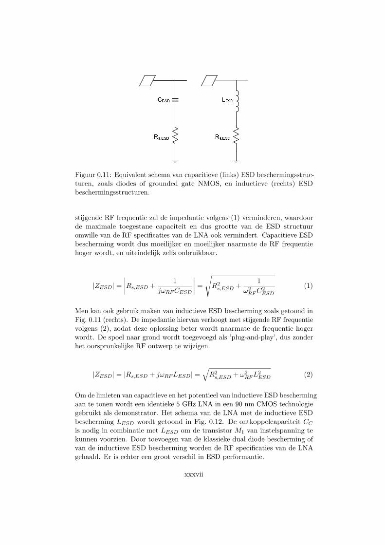
LESDCESDRs,ESD Rs,ESD
Figuur 0.11: Equivalent schema van capacitieve (links) ESD beschermingsstruc-turen, zoals diodes of grounded gate NMOS, en inductieve (rechts) ESDbeschermingsstructuren.
stijgende RF frequentie zal de impedantie volgens (1) verminderen, waardoorde maximale toegestane capaciteit en dus grootte van de ESD structuuromwille van de RF specificaties van de LNA ook vermindert. Capacitieve ESDbescherming wordt dus moeilijker en moeilijker naarmate de RF frequentiehoger wordt, en uiteindelijk zelfs onbruikbaar.
|ZESD| =∣∣∣∣Rs,ESD +
1jωRF CESD
∣∣∣∣ =
√R2
s,ESD +1
ω2RF C2
ESD
(1)
Men kan ook gebruik maken van inductieve ESD bescherming zoals getoond inFig. 0.11 (rechts). De impedantie hiervan verhoogt met stijgende RF frequentievolgens (2), zodat deze oplossing beter wordt naarmate de frequentie hogerwordt. De spoel naar grond wordt toegevoegd als ’plug-and-play’, dus zonderhet oorspronkelijke RF ontwerp te wijzigen.
|ZESD| = |Rs,ESD + jωRF LESD| =√
R2s,ESD + ω2
RF L2ESD (2)
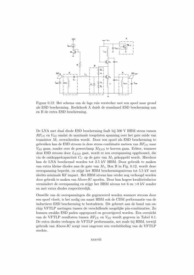
Om de limieten van capacitieve en het potentieel van inductieve ESD beschermingaan te tonen wordt een identieke 5 GHz LNA in een 90 nm CMOS technologiegebruikt als demonstrator. Het schema van de LNA met de inductieve ESDbescherming LESD wordt getoond in Fig. 0.12. De ontkoppelcapaciteit CC
is nodig in combinatie met LESD om de transistor M1 van instelspanning tekunnen voorzien. Door toevoegen van de klassieke dual diode bescherming ofvan de inductieve ESD bescherming worden de RF specificaties van de LNAgehaald. Er is echter een groot verschil in ESD performantie.
xxxvii
RCc LsLg M1
M2LloadVDD
C2RFIN RFOUTLESD LESDCpadC1
MESD
Cpad
CDEC
D3 D2D1D5D4
M1'IBIASA
A
A
B
bias
Figuur 0.12: Het schema van de lage ruis versterker met een spoel naar grondals ESD bescherming. Rechthoek A duidt de standaard ESD bescherming aanen B de extra ESD bescherming.
De LNA met dual diode ESD bescherming faalt bij 500 V HBM stress tussenRFIN en VSS omdat de maximale toegelaten spanning over het gate oxide vantransistor M1 overschreden wordt. Door een spoel als ESD bescherming tegebruiken kan de ESD stroom in deze stress combinatie meteen van RFIN naarVSS gaan, zonder over de powerclamp MESD te hoeven gaan. Echter, wanneerdeze ESD stroom door LESD gaat, wordt er een overspanning opgebouwd, dievia de ontkoppelcapaciteit CC op de gate van M1 gekoppeld wordt. Hierdoorkan de LNA beschermd worden tot 2.5 kV HBM. Door gebruik te makenvan extra kleine diodes aan de gate van M1, Box B in Fig. 0.12, wordt dezeoverspanning beperkt, en stijgt het HBM beschermingsniveau tot 5.5 kV metslechts minimale RF impact. Het HBM niveau kan verder nog verhoogd wordendoor gebruik te maken van Above-IC spoelen. Door hun hogere kwaliteitsfactorvermindert de overspanning en stijgt het HBM niveau tot 6 en >8 kV zonderen met extra diodes respectievelijk.
Omwille van de overspanningen die gegenereerd worden wanneer stroom dooreen spoel vloeit, is het nodig om naast HBM ook de CDM performantie van deinductieve ESD bescherming te bestuderen. Dit gebeurt aan de hand van on-chip VFTLP metingen tussen de verschillende mogelijke pin-combinaties. Zokunnen zwakke ESD paden opgespoord en gecorrigeerd worden. Een overzichtvan de VFTLP resultaten tussen RFIN en VSS wordt gegeven in Tabel 0.1.De extra diodes verhogen de VFTLP performantie, net zoals bij HBM, terwijlgebruik van Above-IC zorgt voor ongeveer een verdubbeling van de VFTLPsterkte.
xxxviii
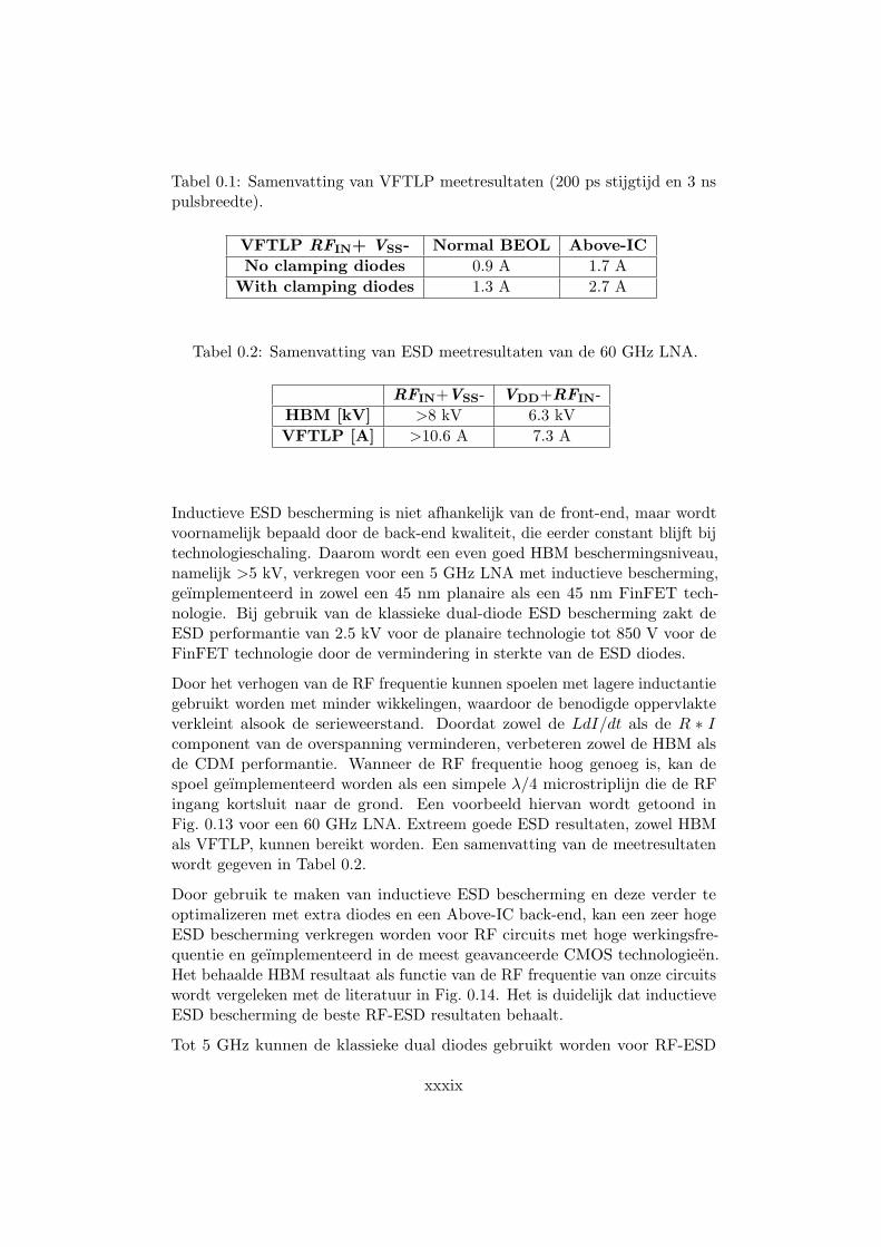
Tabel 0.1: Samenvatting van VFTLP meetresultaten (200 ps stijgtijd en 3 nspulsbreedte).
VFTLP RFIN+ VSS- Normal BEOL Above-ICNo clamping diodes 0.9 A 1.7 A
With clamping diodes 1.3 A 2.7 A
Tabel 0.2: Samenvatting van ESD meetresultaten van de 60 GHz LNA.
RFIN+VSS- VDD+RFIN-HBM [kV] >8 kV 6.3 kVVFTLP [A] >10.6 A 7.3 A
Inductieve ESD bescherming is niet afhankelijk van de front-end, maar wordtvoornamelijk bepaald door de back-end kwaliteit, die eerder constant blijft bijtechnologieschaling. Daarom wordt een even goed HBM beschermingsniveau,namelijk >5 kV, verkregen voor een 5 GHz LNA met inductieve bescherming,geımplementeerd in zowel een 45 nm planaire als een 45 nm FinFET tech-nologie. Bij gebruik van de klassieke dual-diode ESD bescherming zakt deESD performantie van 2.5 kV voor de planaire technologie tot 850 V voor deFinFET technologie door de vermindering in sterkte van de ESD diodes.
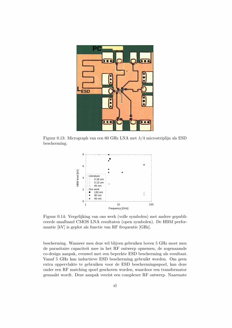
Door het verhogen van de RF frequentie kunnen spoelen met lagere inductantiegebruikt worden met minder wikkelingen, waardoor de benodigde oppervlakteverkleint alsook de serieweerstand. Doordat zowel de LdI/dt als de R ∗ Icomponent van de overspanning verminderen, verbeteren zowel de HBM alsde CDM performantie. Wanneer de RF frequentie hoog genoeg is, kan despoel geımplementeerd worden als een simpele λ/4 microstriplijn die de RFingang kortsluit naar de grond. Een voorbeeld hiervan wordt getoond inFig. 0.13 voor een 60 GHz LNA. Extreem goede ESD resultaten, zowel HBMals VFTLP, kunnen bereikt worden. Een samenvatting van de meetresultatenwordt gegeven in Tabel 0.2.
Door gebruik te maken van inductieve ESD bescherming en deze verder teoptimalizeren met extra diodes en een Above-IC back-end, kan een zeer hogeESD bescherming verkregen worden voor RF circuits met hoge werkingsfre-quentie en geımplementeerd in de meest geavanceerde CMOS technologieen.Het behaalde HBM resultaat als functie van de RF frequentie van onze circuitswordt vergeleken met de literatuur in Fig. 0.14. Het is duidelijk dat inductieveESD bescherming de beste RF-ESD resultaten behaalt.
Tot 5 GHz kunnen de klassieke dual diodes gebruikt worden voor RF-ESD
xxxix
LESD
PC
Figuur 0.13: Micrograph van een 60 GHz LNA met λ/4 microstriplijn als ESDbescherming.
0
2
4
6
8
1 10 100
0.18 um0.13 um45 nm
130 nm90 nm45 nm
HB
M le
vel [
kV]
Frequency [GHz]
Literature
Our work
Figuur 0.14: Vergelijking van ons werk (volle symbolen) met andere gepubli-ceerde smalband CMOS LNA resultaten (open symbolen). De HBM perfor-mantie [kV] is geplot als functie van RF frequentie [GHz].
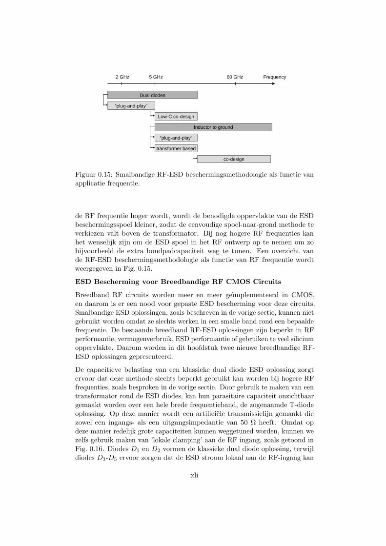
bescherming. Wanneer men deze wil blijven gebruiken boven 5 GHz moet mende parasitaire capaciteit mee in het RF ontwerp opnemen, de zogenaamdeco-design aanpak, evenwel met een beperkte ESD bescherming als resultaat.Vanaf 5 GHz kan inductieve ESD bescherming gebruikt worden. Om geenextra oppervlakte te gebruiken voor de ESD beschermingsspoel, kan dezeonder een RF matching spoel geschoven worden, waardoor een transformatorgemaakt wordt. Deze aanpak vereist een complexer RF ontwerp. Naarmate
xl
Frequency60 GHz5 GHz2 GHz
Dual diodes
“plug-and-play”
Low-C co-design
Inductor to ground
“plug-and-play”
transformer based
co-design
Figuur 0.15: Smalbandige RF-ESD beschermingsmethodologie als functie vanapplicatie frequentie.
de RF frequentie hoger wordt, wordt de benodigde oppervlakte van de ESDbeschermingsspoel kleiner, zodat de eenvoudige spoel-naar-grond methode teverkiezen valt boven de transformator. Bij nog hogere RF frequenties kanhet wenselijk zijn om de ESD spoel in het RF ontwerp op te nemen om zobijvoorbeeld de extra bondpadcapaciteit weg te tunen. Een overzicht vande RF-ESD beschermingsmethodologie als functie van RF frequentie wordtweergegeven in Fig. 0.15.
ESD Bescherming voor Breedbandige RF CMOS Circuits
Breedband RF circuits worden meer en meer geımplementeerd in CMOS,en daarom is er een nood voor gepaste ESD bescherming voor deze circuits.Smalbandige ESD oplossingen, zoals beschreven in de vorige sectie, kunnen nietgebruikt worden omdat ze slechts werken in een smalle band rond een bepaaldefrequentie. De bestaande breedband RF-ESD oplossingen zijn beperkt in RFperformantie, vermogenverbruik, ESD performantie of gebruiken te veel siliciumoppervlakte. Daarom worden in dit hoofdstuk twee nieuwe breedbandige RF-ESD oplossingen gepresenteerd.
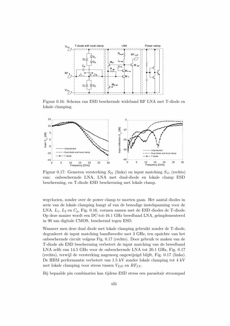
De capacitieve belasting van een klassieke dual diode ESD oplossing zorgtervoor dat deze methode slechts beperkt gebruikt kan worden bij hogere RFfrequenties, zoals besproken in de vorige sectie. Door gebruik te maken van eentransformator rond de ESD diodes, kan hun parasitaire capaciteit onzichtbaargemaakt worden over een hele brede frequentieband, de zogenaamde T-diodeoplossing. Op deze manier wordt een artificiele transmissielijn gemaakt diezowel een ingangs- als een uitgangsimpedantie van 50 Ω heeft. Omdat opdeze manier redelijk grote capaciteiten kunnen weggetuned worden, kunnen wezelfs gebruik maken van ’lokale clamping’ aan de RF ingang, zoals getoond inFig. 0.16. Diodes D1 en D2 vormen de klassieke dual diode oplossing, terwijldiodes D3-D5 ervoor zorgen dat de ESD stroom lokaal aan de RF-ingang kan
xli
Mn1MncasLloadRload
Mn2Mnbias
MnbufVDDVDD
RFINVSS
RFOUTT-diode with local clamp
RbalL1 L2Cp
D5D2 D4
D1 D3
Power clamp
X
LNA
Figuur 0.16: Schema van ESD beschermde wideband RF LNA met T-diode enlokale clamping.
-15
-10
-5
0
5
10
15
0 5 10 15 20 25 30
Unprotected
Dual diode and local clamp
T-diode
Gai
n S
21 [d
B]
Frequency [GHz]
-40
-30
-20
-10
0
0 5 10 15 20 25 30
UnprotectedDual diode and local clampT-diode
Inpu
t ref
lect
ion
S11
[dB
]
Frequency [GHz]
Figuur 0.17: Gemeten versterking S21 (links) en input matching S11 (rechts)van: onbeschermde LNA, LNA met dual-diode en lokale clamp ESDbescherming, en T-diode ESD bescherming met lokale clamp.
wegvloeien, zonder over de power clamp te moeten gaan. Het aantal diodes inserie van de lokale clamping hangt af van de benodige instelspanning voor deLNA. L1, L2 en Cp, Fig. 0.16, vormen samen met de ESD diodes de T-diode.Op deze manier wordt een DC-tot-16.1 GHz breedband LNA, geımplementeerdin 90 nm digitale CMOS, beschermd tegen ESD.
Wanneer men deze dual diode met lokale clamping gebruikt zonder de T-diode,degradeert de input matching bandbreedte met 3 GHz, ten opzichte van hetonbeschermde circuit volgens Fig. 0.17 (rechts). Door gebruik te maken van deT-diode als ESD bescherming verbetert de input matching van de breedbandLNA zelfs van 14.5 GHz voor de onbeschermde LNA tot 20.1 GHz, Fig. 0.17(rechts), terwijl de versterking nagenoeg ongewijzigd blijft, Fig. 0.17 (links).De HBM performantie verbetert van 1.5 kV zonder lokale clamping tot 4 kVmet lokale clamping voor stress tussen VDD en RFIN .
Bij bepaalde pin combinaties kan tijdens ESD stress een parasitair stroompad
xlii
Mn1LloadRload
Mn2Mnbias
Rbal
Turn-offtimer
MncasMnTO
RTOCTO
VSSRFIN
VDD
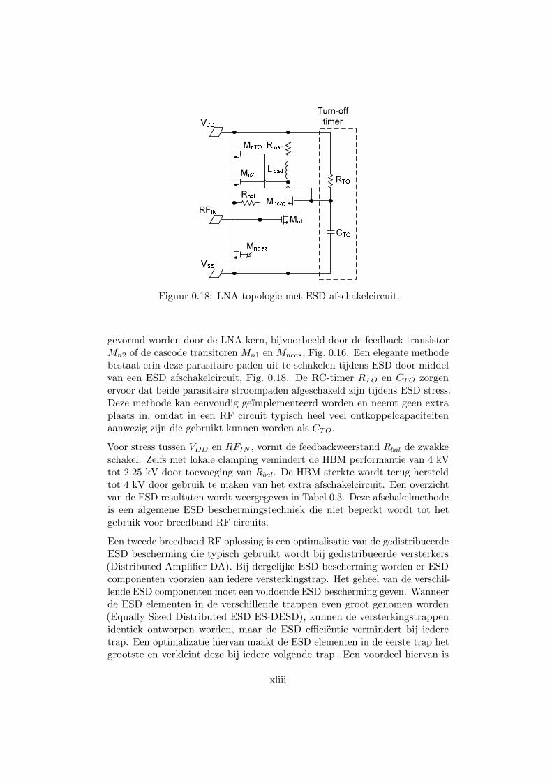
Figuur 0.18: LNA topologie met ESD afschakelcircuit.
gevormd worden door de LNA kern, bijvoorbeeld door de feedback transistorMn2 of de cascode transitoren Mn1 en Mncas, Fig. 0.16. Een elegante methodebestaat erin deze parasitaire paden uit te schakelen tijdens ESD door middelvan een ESD afschakelcircuit, Fig. 0.18. De RC-timer RTO en CTO zorgenervoor dat beide parasitaire stroompaden afgeschakeld zijn tijdens ESD stress.Deze methode kan eenvoudig geımplementeerd worden en neemt geen extraplaats in, omdat in een RF circuit typisch heel veel ontkoppelcapaciteitenaanwezig zijn die gebruikt kunnen worden als CTO.
Voor stress tussen VDD en RFIN , vormt de feedbackweerstand Rbal de zwakkeschakel. Zelfs met lokale clamping vemindert de HBM performantie van 4 kVtot 2.25 kV door toevoeging van Rbal. De HBM sterkte wordt terug hersteldtot 4 kV door gebruik te maken van het extra afschakelcircuit. Een overzichtvan de ESD resultaten wordt weergegeven in Tabel 0.3. Deze afschakelmethodeis een algemene ESD beschermingstechniek die niet beperkt wordt tot hetgebruik voor breedband RF circuits.
Een tweede breedband RF oplossing is een optimalisatie van de gedistribueerdeESD bescherming die typisch gebruikt wordt bij gedistribueerde versterkers(Distributed Amplifier DA). Bij dergelijke ESD bescherming worden er ESDcomponenten voorzien aan iedere versterkingstrap. Het geheel van de verschil-lende ESD componenten moet een voldoende ESD bescherming geven. Wanneerde ESD elementen in de verschillende trappen even groot genomen worden(Equally Sized Distributed ESD ES-DESD), kunnen de versterkingstrappenidentiek ontworpen worden, maar de ESD efficientie vermindert bij iederetrap. Een optimalizatie hiervan maakt de ESD elementen in de eerste trap hetgrootste en verkleint deze bij iedere volgende trap. Een voordeel hiervan is
xliii
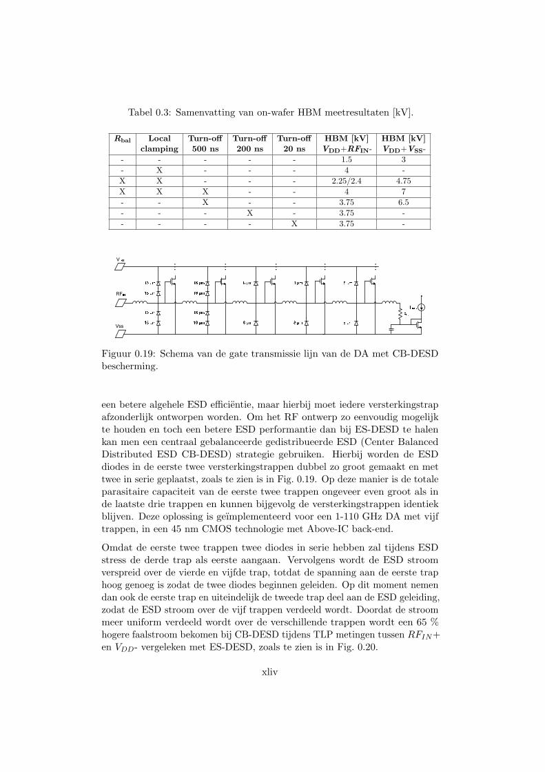
Tabel 0.3: Samenvatting van on-wafer HBM meetresultaten [kV].
Rbal Local Turn-off Turn-off Turn-off HBM [kV] HBM [kV]clamping 500 ns 200 ns 20 ns VDD+RFIN- VDD+VSS-
- - - - - 1.5 3- X - - - 4 -X X - - - 2.25/2.4 4.75X X X - - 4 7- - X - - 3.75 6.5- - - X - 3.75 -- - - - X 3.75 -
RFINVss
VDDRS IBIAS
...
...
...
...
...16 µm16 µm16 µm16 µm
16 µm16 µm16 µm16 µm8 µm8 µm
8 µm8 µm
8 µm8 µm
Figuur 0.19: Schema van de gate transmissie lijn van de DA met CB-DESDbescherming.
een betere algehele ESD efficientie, maar hierbij moet iedere versterkingstrapafzonderlijk ontworpen worden. Om het RF ontwerp zo eenvoudig mogelijkte houden en toch een betere ESD performantie dan bij ES-DESD te halenkan men een centraal gebalanceerde gedistribueerde ESD (Center BalancedDistributed ESD CB-DESD) strategie gebruiken. Hierbij worden de ESDdiodes in de eerste twee versterkingstrappen dubbel zo groot gemaakt en mettwee in serie geplaatst, zoals te zien is in Fig. 0.19. Op deze manier is de totaleparasitaire capaciteit van de eerste twee trappen ongeveer even groot als inde laatste drie trappen en kunnen bijgevolg de versterkingstrappen identiekblijven. Deze oplossing is geımplementeerd voor een 1-110 GHz DA met vijftrappen, in een 45 nm CMOS technologie met Above-IC back-end.
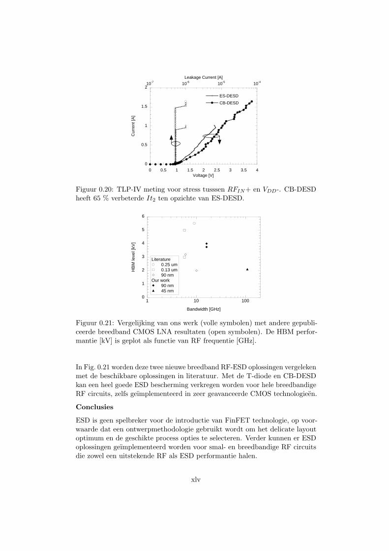
Omdat de eerste twee trappen twee diodes in serie hebben zal tijdens ESDstress de derde trap als eerste aangaan. Vervolgens wordt de ESD stroomverspreid over de vierde en vijfde trap, totdat de spanning aan de eerste traphoog genoeg is zodat de twee diodes beginnen geleiden. Op dit moment nemendan ook de eerste trap en uiteindelijk de tweede trap deel aan de ESD geleiding,zodat de ESD stroom over de vijf trappen verdeeld wordt. Doordat de stroommeer uniform verdeeld wordt over de verschillende trappen wordt een 65 %hogere faalstroom bekomen bij CB-DESD tijdens TLP metingen tussen RFIN+en VDD- vergeleken met ES-DESD, zoals te zien is in Fig. 0.20.
xliv
0
0.5
1
1.5
2
0 0.5 1 1.5 2 2.5 3 3.5 4
10-7 10-6 10-5 10-4
CB-DESD
ES-DESD
Cur
rent
[A]
Voltage [V]
Leakage Current [A]
Figuur 0.20: TLP-IV meting voor stress tusssen RFIN+ en VDD-. CB-DESDheeft 65 % verbeterde It2 ten opzichte van ES-DESD.
0
1
2
3
4
5
6
1 10 100
0.25 um0.13 um90 nm
90 nm45 nm
HB
M le
vel [
kV]
Bandwidth [GHz]
Literature
Our work
Figuur 0.21: Vergelijking van ons werk (volle symbolen) met andere gepubli-ceerde breedband CMOS LNA resultaten (open symbolen). De HBM perfor-mantie [kV] is geplot als functie van RF frequentie [GHz].
In Fig. 0.21 worden deze twee nieuwe breedband RF-ESD oplossingen vergelekenmet de beschikbare oplossingen in literatuur. Met de T-diode en CB-DESDkan een heel goede ESD bescherming verkregen worden voor hele breedbandigeRF circuits, zelfs geımplementeerd in zeer geavanceerde CMOS technologieen.
Conclusies
ESD is geen spelbreker voor de introductie van FinFET technologie, op voor-waarde dat een ontwerpmethodologie gebruikt wordt om het delicate layoutoptimum en de geschikte process opties te selecteren. Verder kunnen er ESDoplossingen geımplementeerd worden voor smal- en breedbandige RF circuitsdie zowel een uitstekende RF als ESD performantie halen.
xlv

Table of Contents
Abstract viiList of Acronyms ixList of Symbols xiiiPublication list xxviiiNederlandstalige Samenvatting xxixTable of Contents xlvii1 Introduction 1
1.1 Reliability in Advanced CMOS Technologies . . . . . . . . . . . 11.2 Electrostatic Discharge in Micro-Electronics . . . . . . . . . . . 21.3 Basic Concepts of ESD Protection . . . . . . . . . . . . . . . . 41.4 Basic ESD Protection Devices . . . . . . . . . . . . . . . . . . . 51.5 ESD Challenges for Technology Scaling . . . . . . . . . . . . . 81.6 ESD Challenges for Radio Frequency CMOS . . . . . . . . . . 101.7 Objectives of the Thesis . . . . . . . . . . . . . . . . . . . . . . 121.8 Outline of the Thesis . . . . . . . . . . . . . . . . . . . . . . . . 12
2 ESD Characterization and Analysis Techniques 152.1 Introduction . . . . . . . . . . . . . . . . . . . . . . . . . . . . . 152.2 Component-Level ESD Stress Models . . . . . . . . . . . . . . . 16
2.2.1 Human Body Model (HBM) . . . . . . . . . . . . . . . . 162.2.2 Machine Model (MM) . . . . . . . . . . . . . . . . . . . 182.2.3 Charged Device Model (CDM) . . . . . . . . . . . . . . 20
2.3 System-Level ESD Stress Models . . . . . . . . . . . . . . . . . 212.3.1 IEC 61000-4-2 . . . . . . . . . . . . . . . . . . . . . . . 222.3.2 Human Metal Model (HMM) . . . . . . . . . . . . . . . 23
2.4 Transmission Line Pulse Measurements (TLP) . . . . . . . . . 242.4.1 Standard 100 ns TLP . . . . . . . . . . . . . . . . . . . 262.4.2 Very Fast TLP (VFTLP) . . . . . . . . . . . . . . . . . 272.4.3 Capacitive Coupled TLP (CCTLP) . . . . . . . . . . . . 30
2.5 Enhanced ESD Characterization and Analysis Techniques . . . 312.5.1 Multi-level TLP . . . . . . . . . . . . . . . . . . . . . . 312.5.2 Transient analysis using TLP . . . . . . . . . . . . . . . 342.5.3 HBM-IV . . . . . . . . . . . . . . . . . . . . . . . . . . . 40
2.6 Conclusions . . . . . . . . . . . . . . . . . . . . . . . . . . . . . 51
xlvii
3 ESD Protection in FinFET Technology 533.1 Introduction . . . . . . . . . . . . . . . . . . . . . . . . . . . . . 533.2 FinFET Technology . . . . . . . . . . . . . . . . . . . . . . . . 543.3 Normalization Methodology . . . . . . . . . . . . . . . . . . . . 553.4 Geometrical Dependencies . . . . . . . . . . . . . . . . . . . . . 58
3.4.1 MOS devices - parasitic bipolar mode . . . . . . . . . . 583.4.2 MOS devices - active MOS-diode mode . . . . . . . . . 803.4.3 Gated diodes . . . . . . . . . . . . . . . . . . . . . . . . 82
3.5 Benchmarking against Advanced CMOS Technology Nodes . . 853.6 Process Technology Dependencies . . . . . . . . . . . . . . . . . 88
3.6.1 Extension implants . . . . . . . . . . . . . . . . . . . . . 883.6.2 Fin doping on wide fin devices . . . . . . . . . . . . . . 893.6.3 Selective Epitaxial Growth . . . . . . . . . . . . . . . . 913.6.4 Silicide Blocking . . . . . . . . . . . . . . . . . . . . . . 953.6.5 Strain . . . . . . . . . . . . . . . . . . . . . . . . . . . . 96
3.7 Gated Diodes - RF Considerations, Transient Analysis andModeling . . . . . . . . . . . . . . . . . . . . . . . . . . . . . . 1053.7.1 RF considerations . . . . . . . . . . . . . . . . . . . . . 1063.7.2 Transient analysis and compact modeling . . . . . . . . 107
3.8 Design Methodology . . . . . . . . . . . . . . . . . . . . . . . . 1173.8.1 MOS devices - parasitic bipolar mode . . . . . . . . . . 1183.8.2 MOS devices - active MOS diode mode . . . . . . . . . 1253.8.3 Optimization constraint trajectory . . . . . . . . . . . . 1283.8.4 Bidirectional power clamp . . . . . . . . . . . . . . . . . 132
3.9 Conclusions . . . . . . . . . . . . . . . . . . . . . . . . . . . . . 1364 ESD Protection for Narrowband RF CMOS Circuits 139
4.1 Introduction . . . . . . . . . . . . . . . . . . . . . . . . . . . . . 1394.2 Dual Diode Methodology . . . . . . . . . . . . . . . . . . . . . 1454.3 Codesign Methodology . . . . . . . . . . . . . . . . . . . . . . . 1474.4 Inductor to Ground Methodology . . . . . . . . . . . . . . . . . 149
4.4.1 Back-end of line (BEOL) inductor . . . . . . . . . . . . 1504.4.2 Above-IC inductor . . . . . . . . . . . . . . . . . . . . . 1554.4.3 VFTLP results . . . . . . . . . . . . . . . . . . . . . . . 1584.4.4 Overall comparison . . . . . . . . . . . . . . . . . . . . . 161
4.5 Scaling Aspects of Inductor to Ground Approach . . . . . . . . 1614.5.1 5 GHz LNA in 45 nm planar and FinFET CMOS tech-
nology . . . . . . . . . . . . . . . . . . . . . . . . . . . . 1634.5.2 13 GHz LNA in 45 nm planar CMOS technology with
Above-IC inductors . . . . . . . . . . . . . . . . . . . . . 1644.5.3 60 GHz LNA in 45 nm planar CMOS technology with
Above-IC inductors . . . . . . . . . . . . . . . . . . . . . 1644.5.4 60 GHz PA in 45 nm planar digital CMOS technology . 1664.5.5 Discussion . . . . . . . . . . . . . . . . . . . . . . . . . . 172
4.6 Transformer Based Methodology . . . . . . . . . . . . . . . . . 173
xlviii
4.7 State-of-the-Art Comparison . . . . . . . . . . . . . . . . . . . 1794.8 Conclusions . . . . . . . . . . . . . . . . . . . . . . . . . . . . . 180
5 ESD Protection for Wideband RF CMOS Circuits 1835.1 Introduction . . . . . . . . . . . . . . . . . . . . . . . . . . . . . 1835.2 T-diodes . . . . . . . . . . . . . . . . . . . . . . . . . . . . . . . 184
5.2.1 T-diode design methodology . . . . . . . . . . . . . . . . 1845.2.2 Symmetric T-diode . . . . . . . . . . . . . . . . . . . . . 1885.2.3 Asymmetric T-diode with built-in local ESD protection 1965.2.4 ESD turn-off circuit . . . . . . . . . . . . . . . . . . . . 202
5.3 Center Balanced Distributed ESD Methodology . . . . . . . . . 2055.4 State-of-the-Art Comparison . . . . . . . . . . . . . . . . . . . 2135.5 Conclusions . . . . . . . . . . . . . . . . . . . . . . . . . . . . . 216
6 Conclusions, Future Work and Outlook 2176.1 Conclusions . . . . . . . . . . . . . . . . . . . . . . . . . . . . . 2176.2 Future Work . . . . . . . . . . . . . . . . . . . . . . . . . . . . 2196.3 Outlook . . . . . . . . . . . . . . . . . . . . . . . . . . . . . . . 221
Bibliography 223
xlix

Chapter 1
Introduction
The reliability of the microelectronic devices and circuits is a major factorthat determines both their manufacturability and application lifetime. Designfor reliability should be implemented during technology, device and circuitdevelopment to avoid undesirable product development cycles and costly yieldloss and field failures. The specific reliability problem studied in this PhD iscaused by ElectroStatic Discharge (ESD) events.
1.1 Reliability in Advanced CMOS Technologies
With the continuous downscaling of Complimentary Metal Oxide Semiconduc-tor (CMOS) technologies, reliability has become a major bottleneck, on theone hand due to the continuous increase in internal electrical fields and currentdensities, and on the other hand due to the introduction of new materialsand device architectures with unknown reliability behavior. When the devicegeometries are scaled into the range needed for 65 nm CMOS technologies andbelow, the available reliability margins are strongly reduced, in some caseseven down to zero. As a result, the reliability community will be obliged tolook more in detail to what exactly is determining these margins, and howwe can change our reliability assessment methodology to gain new reliabilityspace for the most advanced technologies.
A big variety of failure mechanisms needs to be investigated, such as hot carrierdegradation, time-dependent dielectric breakdown, negative bias temperatureinstability, electromigration, stress voiding, interconnect dielectric instabilityand breakdown, and electrostatic discharge. Each of these reliability mecha-nisms has its own set of issues associated with technology scaling. This PhDfocusses on reliability problems associated with ESD events.
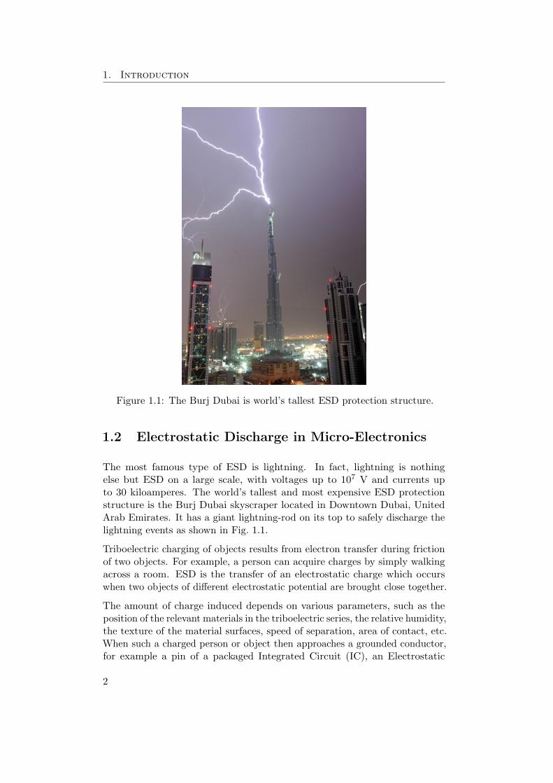
1. Introduction
Figure 1.1: The Burj Dubai is world’s tallest ESD protection structure.
1.2 Electrostatic Discharge in Micro-Electronics
The most famous type of ESD is lightning. In fact, lightning is nothingelse but ESD on a large scale, with voltages up to 107 V and currents upto 30 kiloamperes. The world’s tallest and most expensive ESD protectionstructure is the Burj Dubai skyscraper located in Downtown Dubai, UnitedArab Emirates. It has a giant lightning-rod on its top to safely discharge thelightning events as shown in Fig. 1.1.
Triboelectric charging of objects results from electron transfer during frictionof two objects. For example, a person can acquire charges by simply walkingacross a room. ESD is the transfer of an electrostatic charge which occurswhen two objects of different electrostatic potential are brought close together.
The amount of charge induced depends on various parameters, such as theposition of the relevant materials in the triboelectric series, the relative humidity,the texture of the material surfaces, speed of separation, area of contact, etc.When such a charged person or object then approaches a grounded conductor,for example a pin of a packaged Integrated Circuit (IC), an Electrostatic
2
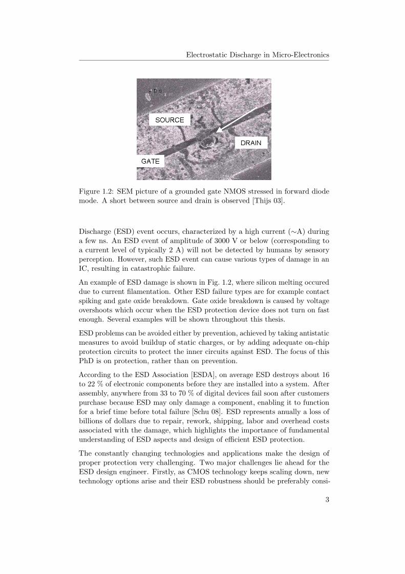
Electrostatic Discharge in Micro-Electronics
Figure 1.2: SEM picture of a grounded gate NMOS stressed in forward diodemode. A short between source and drain is observed [Thijs 03].
Discharge (ESD) event occurs, characterized by a high current (∼A) duringa few ns. An ESD event of amplitude of 3000 V or below (corresponding toa current level of typically 2 A) will not be detected by humans by sensoryperception. However, such ESD event can cause various types of damage in anIC, resulting in catastrophic failure.
An example of ESD damage is shown in Fig. 1.2, where silicon melting occureddue to current filamentation. Other ESD failure types are for example contactspiking and gate oxide breakdown. Gate oxide breakdown is caused by voltageovershoots which occur when the ESD protection device does not turn on fastenough. Several examples will be shown throughout this thesis.
ESD problems can be avoided either by prevention, achieved by taking antistaticmeasures to avoid buildup of static charges, or by adding adequate on-chipprotection circuits to protect the inner circuits against ESD. The focus of thisPhD is on protection, rather than on prevention.
According to the ESD Association [ESDA], on average ESD destroys about 16to 22 % of electronic components before they are installed into a system. Afterassembly, anywhere from 33 to 70 % of digital devices fail soon after customerspurchase because ESD may only damage a component, enabling it to functionfor a brief time before total failure [Schu 08]. ESD represents anually a loss ofbillions of dollars due to repair, rework, shipping, labor and overhead costsassociated with the damage, which highlights the importance of fundamentalunderstanding of ESD aspects and design of efficient ESD protection.
The constantly changing technologies and applications make the design ofproper protection very challenging. Two major challenges lie ahead for theESD design engineer. Firstly, as CMOS technology keeps scaling down, newtechnology options arise and their ESD robustness should be preferably consi-
3
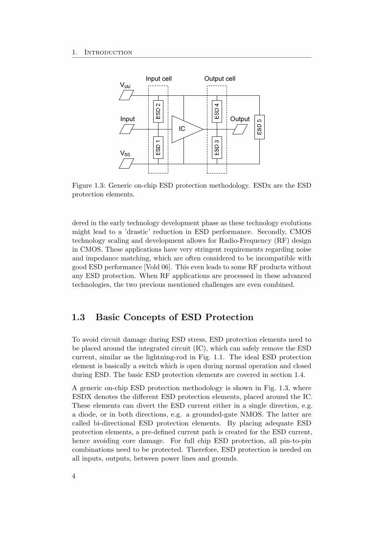
1. Introduction
Input
VSSOutput
ESD 1ESD 2
ESD 3ESD 4 ESD 5
Input cell Output cellVDD
IC
Figure 1.3: Generic on-chip ESD protection methodology. ESDx are the ESDprotection elements.
dered in the early technology development phase as these technology evolutionsmight lead to a ’drastic’ reduction in ESD performance. Secondly, CMOStechnology scaling and development allows for Radio-Frequency (RF) designin CMOS. These applications have very stringent requirements regarding noiseand impedance matching, which are often considered to be incompatible withgood ESD performance [Vold 06]. This even leads to some RF products withoutany ESD protection. When RF applications are processed in these advancedtechnologies, the two previous mentioned challenges are even combined.
1.3 Basic Concepts of ESD Protection
To avoid circuit damage during ESD stress, ESD protection elements need tobe placed around the integrated circuit (IC), which can safely remove the ESDcurrent, similar as the lightning-rod in Fig. 1.1. The ideal ESD protectionelement is basically a switch which is open during normal operation and closedduring ESD. The basic ESD protection elements are covered in section 1.4.
A generic on-chip ESD protection methodology is shown in Fig. 1.3, whereESDX denotes the different ESD protection elements, placed around the IC.These elements can divert the ESD current either in a single direction, e.g.a diode, or in both directions, e.g. a grounded-gate NMOS. The latter arecalled bi-directional ESD protection elements. By placing adequate ESDprotection elements, a pre-defined current path is created for the ESD current,hence avoiding core damage. For full chip ESD protection, all pin-to-pincombinations need to be protected. Therefore, ESD protection is needed onall inputs, outputs, between power lines and grounds.
4
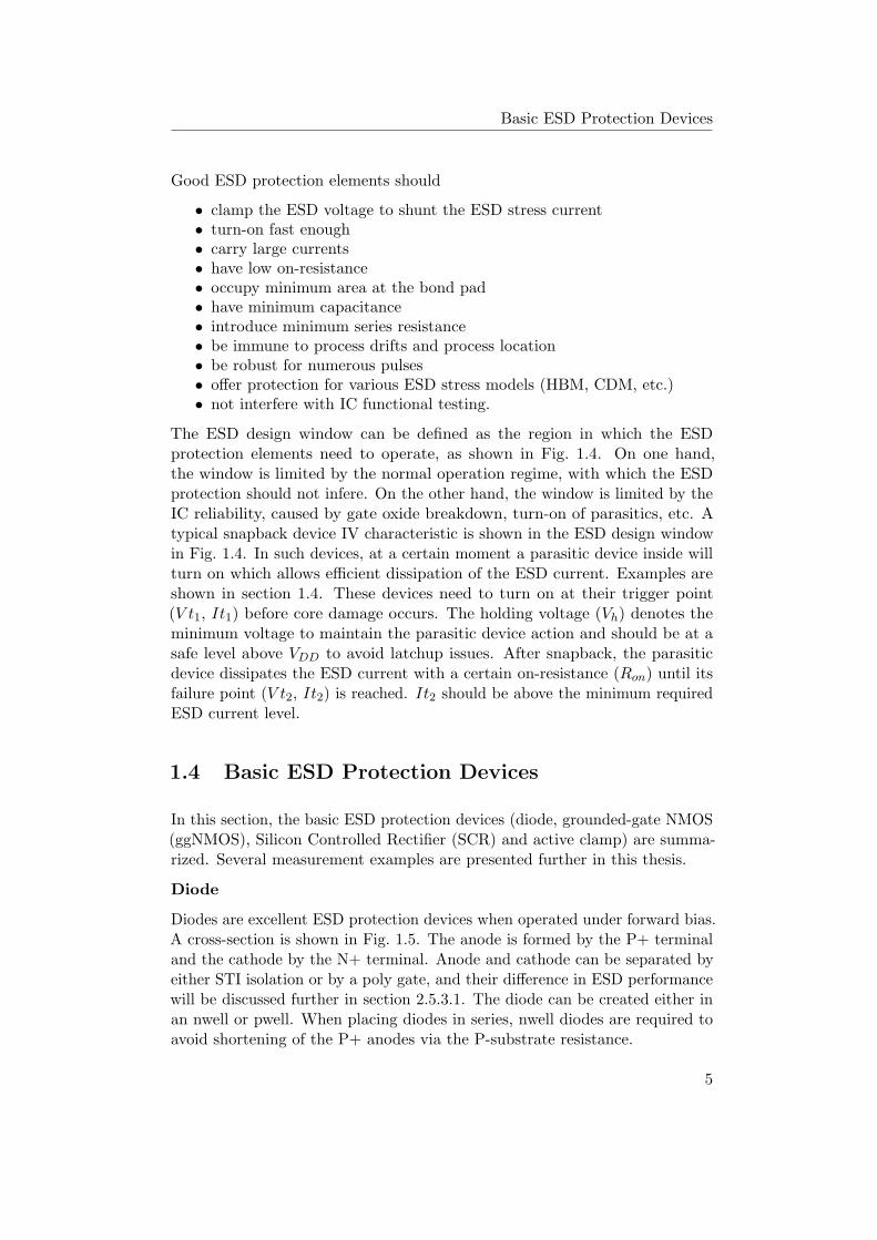
Basic ESD Protection Devices
Good ESD protection elements should
• clamp the ESD voltage to shunt the ESD stress current• turn-on fast enough• carry large currents• have low on-resistance• occupy minimum area at the bond pad• have minimum capacitance• introduce minimum series resistance• be immune to process drifts and process location• be robust for numerous pulses• offer protection for various ESD stress models (HBM, CDM, etc.)• not interfere with IC functional testing.
The ESD design window can be defined as the region in which the ESDprotection elements need to operate, as shown in Fig. 1.4. On one hand,the window is limited by the normal operation regime, with which the ESDprotection should not infere. On the other hand, the window is limited by theIC reliability, caused by gate oxide breakdown, turn-on of parasitics, etc. Atypical snapback device IV characteristic is shown in the ESD design windowin Fig. 1.4. In such devices, at a certain moment a parasitic device inside willturn on which allows efficient dissipation of the ESD current. Examples areshown in section 1.4. These devices need to turn on at their trigger point(V t1, It1) before core damage occurs. The holding voltage (Vh) denotes theminimum voltage to maintain the parasitic device action and should be at asafe level above VDD to avoid latchup issues. After snapback, the parasiticdevice dissipates the ESD current with a certain on-resistance (Ron) until itsfailure point (V t2, It2) is reached. It2 should be above the minimum requiredESD current level.
1.4 Basic ESD Protection Devices
In this section, the basic ESD protection devices (diode, grounded-gate NMOS(ggNMOS), Silicon Controlled Rectifier (SCR) and active clamp) are summa-rized. Several measurement examples are presented further in this thesis.
Diode
Diodes are excellent ESD protection devices when operated under forward bias.A cross-section is shown in Fig. 1.5. The anode is formed by the P+ terminaland the cathode by the N+ terminal. Anode and cathode can be separated byeither STI isolation or by a poly gate, and their difference in ESD performancewill be discussed further in section 2.5.3.1. The diode can be created either inan nwell or pwell. When placing diodes in series, nwell diodes are required toavoid shortening of the P+ anodes via the P-substrate resistance.
5
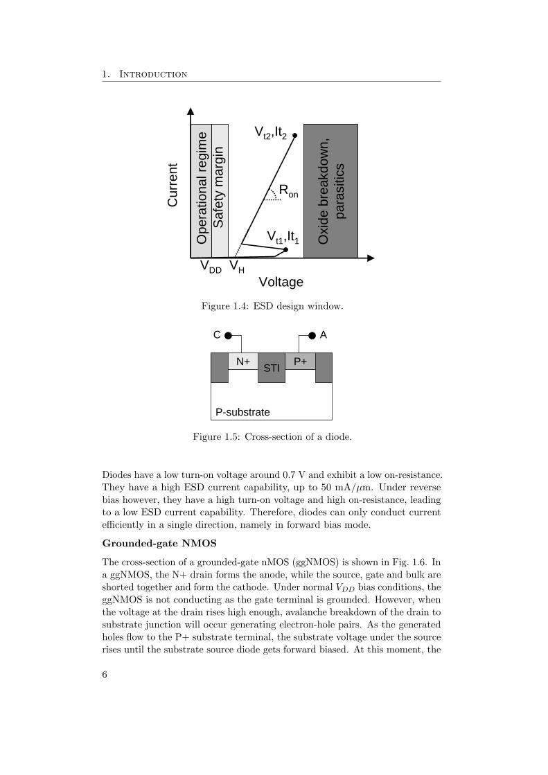
1. Introduction
Ope
ratio
nal r
egim
e
Voltage
Cur
rent
Oxi
de b
reak
dow
n,pa
rasi
tics
VDD
Saf
ety
mar
gin
VH
Vt1,It1
Vt2,It2
Ron
Figure 1.4: ESD design window.
STIN+ P+
C A
P-substrate
Figure 1.5: Cross-section of a diode.
Diodes have a low turn-on voltage around 0.7 V and exhibit a low on-resistance.They have a high ESD current capability, up to 50 mA/µm. Under reversebias however, they have a high turn-on voltage and high on-resistance, leadingto a low ESD current capability. Therefore, diodes can only conduct currentefficiently in a single direction, namely in forward bias mode.
Grounded-gate NMOS
The cross-section of a grounded-gate nMOS (ggNMOS) is shown in Fig. 1.6. Ina ggNMOS, the N+ drain forms the anode, while the source, gate and bulk areshorted together and form the cathode. Under normal VDD bias conditions, theggNMOS is not conducting as the gate terminal is grounded. However, whenthe voltage at the drain rises high enough, avalanche breakdown of the drain tosubstrate junction will occur generating electron-hole pairs. As the generatedholes flow to the P+ substrate terminal, the substrate voltage under the sourcerises until the substrate source diode gets forward biased. At this moment, the
6
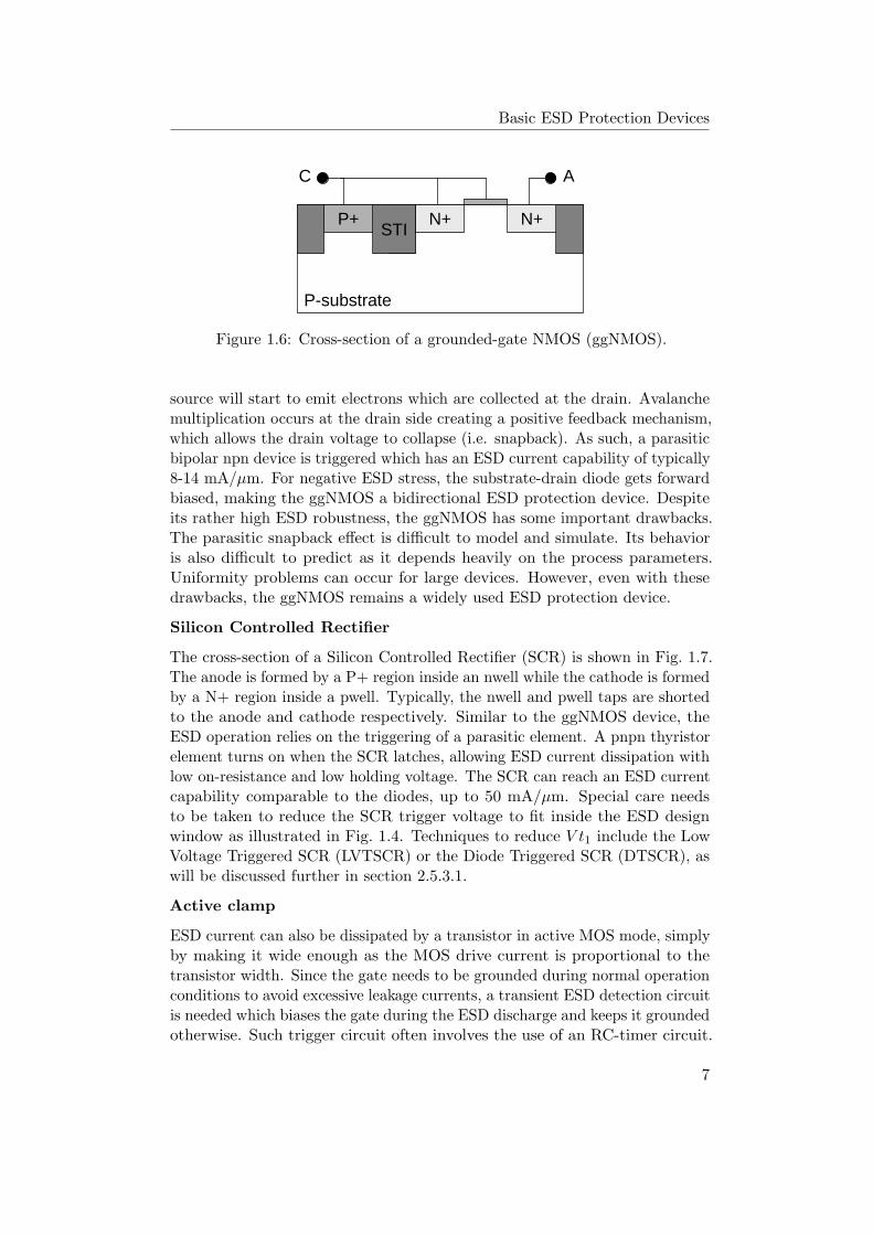
Basic ESD Protection Devices
STIN+
A
P+ N+
C
P-substrate
Figure 1.6: Cross-section of a grounded-gate NMOS (ggNMOS).
source will start to emit electrons which are collected at the drain. Avalanchemultiplication occurs at the drain side creating a positive feedback mechanism,which allows the drain voltage to collapse (i.e. snapback). As such, a parasiticbipolar npn device is triggered which has an ESD current capability of typically8-14 mA/µm. For negative ESD stress, the substrate-drain diode gets forwardbiased, making the ggNMOS a bidirectional ESD protection device. Despiteits rather high ESD robustness, the ggNMOS has some important drawbacks.The parasitic snapback effect is difficult to model and simulate. Its behavioris also difficult to predict as it depends heavily on the process parameters.Uniformity problems can occur for large devices. However, even with thesedrawbacks, the ggNMOS remains a widely used ESD protection device.
Silicon Controlled Rectifier
The cross-section of a Silicon Controlled Rectifier (SCR) is shown in Fig. 1.7.The anode is formed by a P+ region inside an nwell while the cathode is formedby a N+ region inside a pwell. Typically, the nwell and pwell taps are shortedto the anode and cathode respectively. Similar to the ggNMOS device, theESD operation relies on the triggering of a parasitic element. A pnpn thyristorelement turns on when the SCR latches, allowing ESD current dissipation withlow on-resistance and low holding voltage. The SCR can reach an ESD currentcapability comparable to the diodes, up to 50 mA/µm. Special care needsto be taken to reduce the SCR trigger voltage to fit inside the ESD designwindow as illustrated in Fig. 1.4. Techniques to reduce V t1 include the LowVoltage Triggered SCR (LVTSCR) or the Diode Triggered SCR (DTSCR), aswill be discussed further in section 2.5.3.1.
Active clamp
ESD current can also be dissipated by a transistor in active MOS mode, simplyby making it wide enough as the MOS drive current is proportional to thetransistor width. Since the gate needs to be grounded during normal operationconditions to avoid excessive leakage currents, a transient ESD detection circuitis needed which biases the gate during the ESD discharge and keeps it groundedotherwise. Such trigger circuit often involves the use of an RC-timer circuit.
7
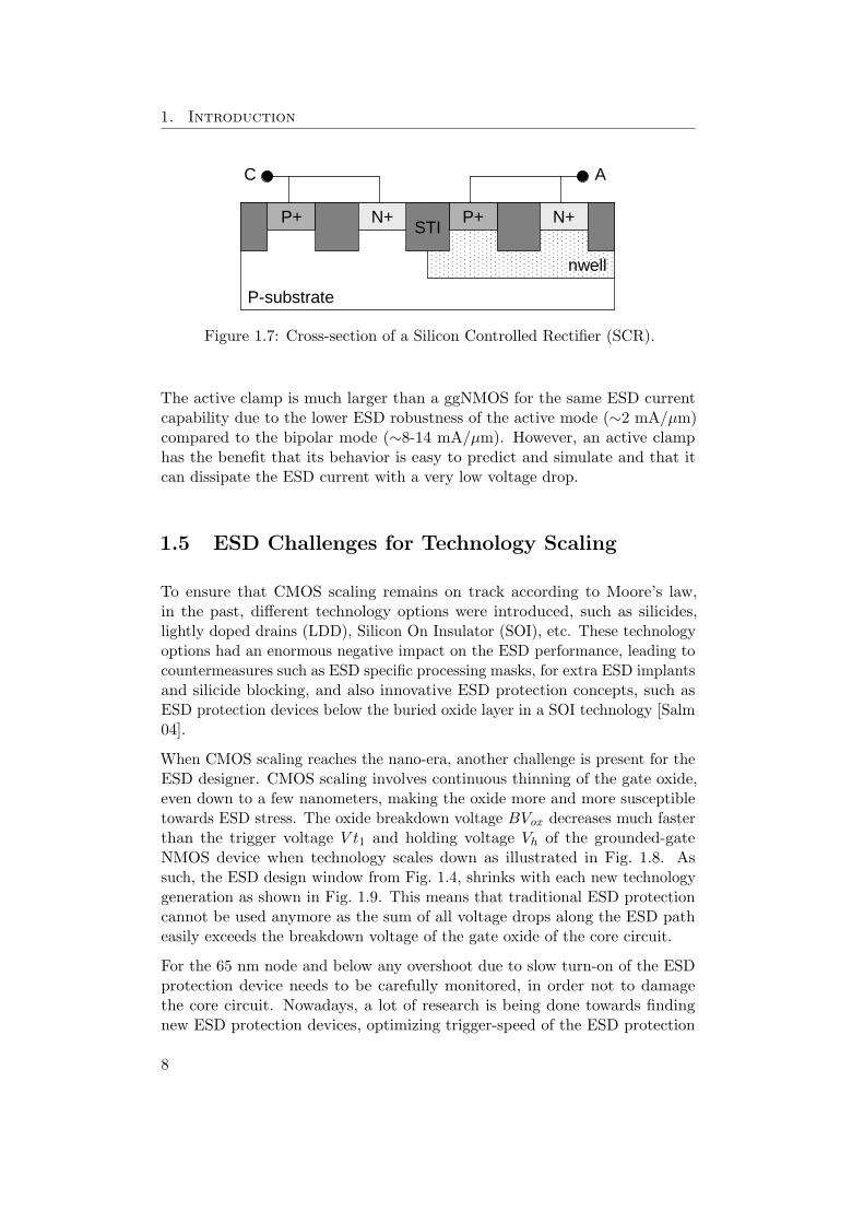
1. Introduction
N+
A
P+
C
P+STI
N+
nwell
P-substrate
Figure 1.7: Cross-section of a Silicon Controlled Rectifier (SCR).
The active clamp is much larger than a ggNMOS for the same ESD currentcapability due to the lower ESD robustness of the active mode (∼2 mA/µm)compared to the bipolar mode (∼8-14 mA/µm). However, an active clamphas the benefit that its behavior is easy to predict and simulate and that itcan dissipate the ESD current with a very low voltage drop.
1.5 ESD Challenges for Technology Scaling
To ensure that CMOS scaling remains on track according to Moore’s law,in the past, different technology options were introduced, such as silicides,lightly doped drains (LDD), Silicon On Insulator (SOI), etc. These technologyoptions had an enormous negative impact on the ESD performance, leading tocountermeasures such as ESD specific processing masks, for extra ESD implantsand silicide blocking, and also innovative ESD protection concepts, such asESD protection devices below the buried oxide layer in a SOI technology [Salm04].
When CMOS scaling reaches the nano-era, another challenge is present for theESD designer. CMOS scaling involves continuous thinning of the gate oxide,even down to a few nanometers, making the oxide more and more susceptibletowards ESD stress. The oxide breakdown voltage BVox decreases much fasterthan the trigger voltage V t1 and holding voltage Vh of the grounded-gateNMOS device when technology scales down as illustrated in Fig. 1.8. Assuch, the ESD design window from Fig. 1.4, shrinks with each new technologygeneration as shown in Fig. 1.9. This means that traditional ESD protectioncannot be used anymore as the sum of all voltage drops along the ESD patheasily exceeds the breakdown voltage of the gate oxide of the core circuit.
For the 65 nm node and below any overshoot due to slow turn-on of the ESDprotection device needs to be carefully monitored, in order not to damagethe core circuit. Nowadays, a lot of research is being done towards findingnew ESD protection devices, optimizing trigger-speed of the ESD protection
8
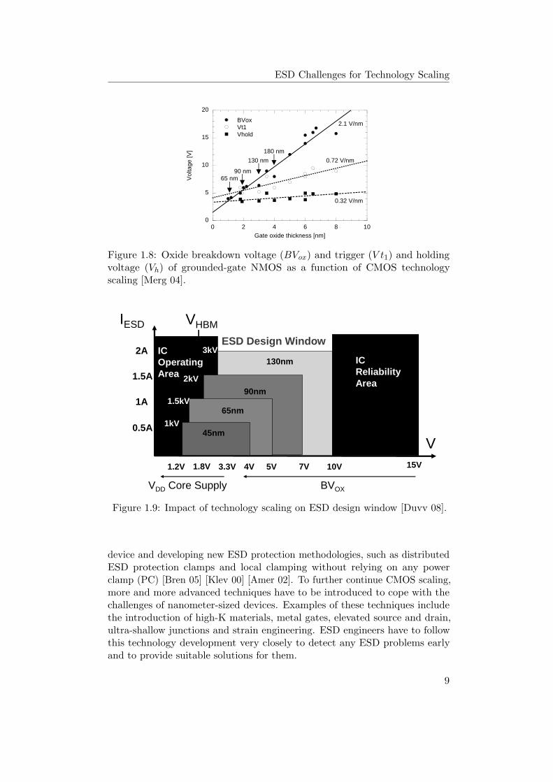
ESD Challenges for Technology Scaling
0
5
10
15
20
0 2 4 6 8 10
BVoxVt1Vhold
Vol
tage
[V]
Gate oxide thickness [nm]
2.1 V/nm
0.72 V/nm
0.32 V/nm
65 nm90 nm
130 nm
180 nm
Figure 1.8: Oxide breakdown voltage (BVox ) and trigger (V t1) and holdingvoltage (Vh) of grounded-gate NMOS as a function of CMOS technologyscaling [Merg 04].
IESD
1.2V 1.8V 3.3V 5V 7V 10V
65nm
90nm
130nm
VDD Core Supply BVOX
IC Operating Area
IC Reliability Area
15V
V
ESD Design Window
VHBM
3kV
2kV
1.5kV
2A
1.5A
1A
45nm1kV
4V
0.5A
Figure 1.9: Impact of technology scaling on ESD design window [Duvv 08].
device and developing new ESD protection methodologies, such as distributedESD protection clamps and local clamping without relying on any powerclamp (PC) [Bren 05] [Klev 00] [Amer 02]. To further continue CMOS scaling,more and more advanced techniques have to be introduced to cope with thechallenges of nanometer-sized devices. Examples of these techniques includethe introduction of high-K materials, metal gates, elevated source and drain,ultra-shallow junctions and strain engineering. ESD engineers have to followthis technology development very closely to detect any ESD problems earlyand to provide suitable solutions for them.
9
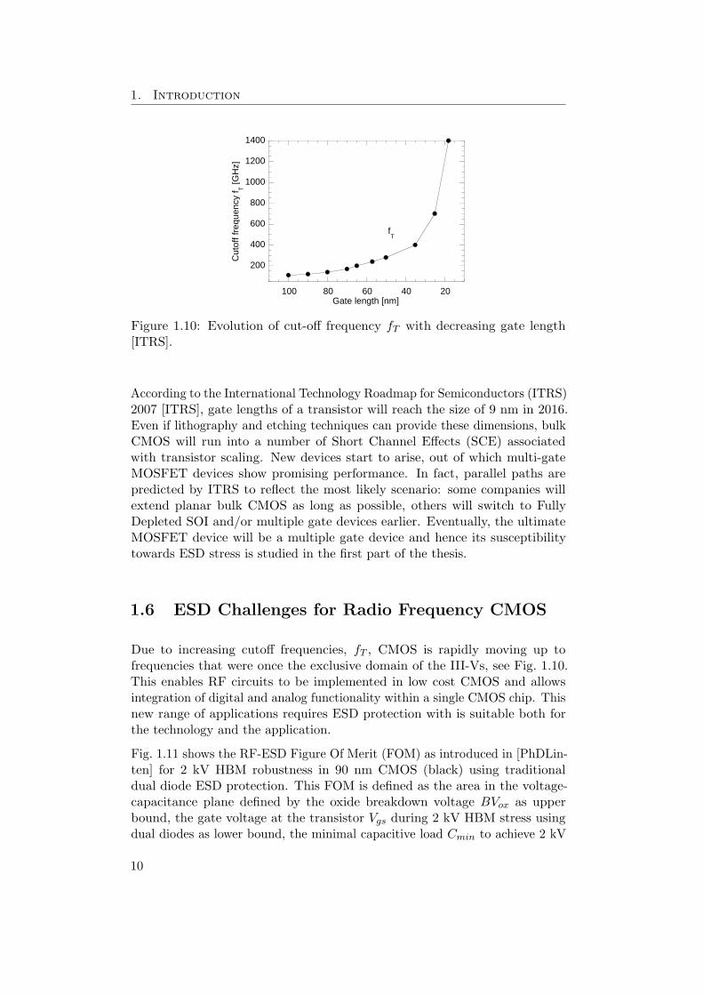
1. Introduction
200
400
600
800
1000
1200
1400
20406080100
Cut
off f
requ
ency
f T [G
Hz]
Gate length [nm]
ITRS 2003
fT
Figure 1.10: Evolution of cut-off frequency fT with decreasing gate length[ITRS].
According to the International Technology Roadmap for Semiconductors (ITRS)2007 [ITRS], gate lengths of a transistor will reach the size of 9 nm in 2016.Even if lithography and etching techniques can provide these dimensions, bulkCMOS will run into a number of Short Channel Effects (SCE) associatedwith transistor scaling. New devices start to arise, out of which multi-gateMOSFET devices show promising performance. In fact, parallel paths arepredicted by ITRS to reflect the most likely scenario: some companies willextend planar bulk CMOS as long as possible, others will switch to FullyDepleted SOI and/or multiple gate devices earlier. Eventually, the ultimateMOSFET device will be a multiple gate device and hence its susceptibilitytowards ESD stress is studied in the first part of the thesis.
1.6 ESD Challenges for Radio Frequency CMOS
Due to increasing cutoff frequencies, fT , CMOS is rapidly moving up tofrequencies that were once the exclusive domain of the III-Vs, see Fig. 1.10.This enables RF circuits to be implemented in low cost CMOS and allowsintegration of digital and analog functionality within a single CMOS chip. Thisnew range of applications requires ESD protection with is suitable both forthe technology and the application.
Fig. 1.11 shows the RF-ESD Figure Of Merit (FOM) as introduced in [PhDLin-ten] for 2 kV HBM robustness in 90 nm CMOS (black) using traditionaldual diode ESD protection. This FOM is defined as the area in the voltage-capacitance plane defined by the oxide breakdown voltage BVox as upperbound, the gate voltage at the transistor Vgs during 2 kV HBM stress usingdual diodes as lower bound, the minimal capacitive load Cmin to achieve 2 kV
10
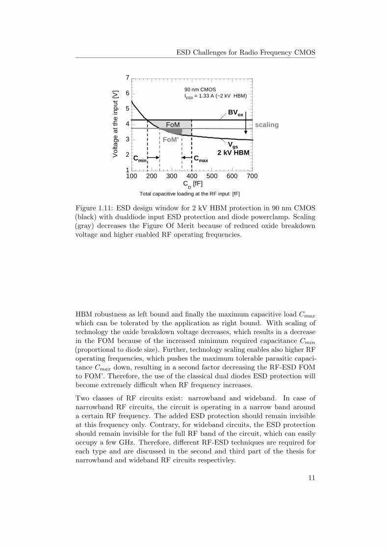
ESD Challenges for Radio Frequency CMOS
1
2
3
4
5
6
7
100 200 300 400 500 600 700
Vol
tage
at t
he in
put
[V]
CD [fF]
BVox
Vgs2 kV HBM
Cmin Cmax
FoM scaling
FoM’
90 nm CMOSIESD = 1.33 A (~2 kV HBM)
Total capacitive loading at the RF input [fF]
Figure 1.11: ESD design window for 2 kV HBM protection in 90 nm CMOS(black) with dualdiode input ESD protection and diode powerclamp. Scaling(gray) decreases the Figure Of Merit because of reduced oxide breakdownvoltage and higher enabled RF operating frequencies.
HBM robustness as left bound and finally the maximum capacitive load Cmax
which can be tolerated by the application as right bound. With scaling oftechnology the oxide breakdown voltage decreases, which results in a decreasein the FOM because of the increased minimum required capacitance Cmin
(proportional to diode size). Further, technology scaling enables also higher RFoperating frequencies, which pushes the maximum tolerable parasitic capaci-tance Cmax down, resulting in a second factor decreasing the RF-ESD FOMto FOM’. Therefore, the use of the classical dual diodes ESD protection willbecome extremely difficult when RF frequency increases.
Two classes of RF circuits exist: narrowband and wideband. In case ofnarrowband RF circuits, the circuit is operating in a narrow band arounda certain RF frequency. The added ESD protection should remain invisibleat this frequency only. Contrary, for wideband circuits, the ESD protectionshould remain invisible for the full RF band of the circuit, which can easilyoccupy a few GHz. Therefore, different RF-ESD techniques are required foreach type and are discussed in the second and third part of the thesis fornarrowband and wideband RF circuits respectivley.
11
1. Introduction
1.7 Objectives of the Thesis
This thesis has two main objectives, namely to investigate the ESD robustnessof the upcoming FinFET technology and to propose ESD solutions which arecompatible with narrow- and wideband RF applications.
Our first main objective is to investigate whether ESD is a potential showstop-per for the introduction of FinFET technology. This is achieved by analyzingthe ESD capability of basic ESD protection devices implemented in FinFETtechnology, such as gated diodes and MOS transistors operating in both positiveand negative polarities. The 3D-nature of FinFET devices offers an increasedset of geometrical parameters compared to planar transistors. Their impacton the ESD robustness needs to be evaluated. Further, as different processoptions are introduced to improve the overall FinFET performance, also theirimpact on the ESD performance of the different devices needs to be qualified.
The second main objective is to provide adequate ESD protection for RF appli-cations. RF circuits are being implemented more and more in advanced CMOStechnologies and reach ever higher operating frequencies, demanding for newRF-ESD solutions. The objective is to propose new protection methodologiesfor both narrow- and wideband RF circuits meeting these requirements. Thesolutions need to be qualified for their RF and ESD impact and need to bebenchmarked against traditional and new innovative solutions. A specificemphasis on Charged Device Model (CDM) robustness is also required.
1.8 Outline of the Thesis
A summary of the different chapters of this thesis is provided below.
Chapter 2: ESD Characterization and Analysis Techniques
Commonly used ESD characterization and analysis techniques are summarizedin the first part of the chapter. These ESD test methods are extended to givemore information regarding transient device behavior under both TransmissionLine Pulse (TLP) and Human Body Model (HBM) conditions and extractingof the real holding voltage and current for snapback devices.
Chapter 3: ESD Protection in FinFET Technology
In this chapter, the ESD robustness of the new emerging FinFET technologyis evaluated. A fundamental understanding of the physics of the devicesunder ESD stress conditions is the main part of this chapter. To acquire thisunderstanding, extensive test structures are designed and characterized, whileTechnology Computer Aided Design (TCAD) computer simulations are usedfor gaining deeper physical insights. Based on this knowledge, a new ESD
12
Outline of the Thesis
protection methodology is developed.
Chapter 4: ESD Protection for Narrowband RF CMOS Circuits
The implementation of adequate on-chip ESD protection for narrowband RFCMOS applications is addressed in this chapter. This requires addressing bothdesign and technology limiting challenges. As operation frequencies keep onincreasing, the simple dual-diode ESD protection is not viable anymore as theparasitic capacitance of the diodes will degrade the impedance matching ofthe RF circuit. Therefore, other innovative solutions are needed for adequateRF-ESD protection. One of the most promising solutions was found to beinductor-based ESD protection. However, a major concern for RF ESDprotection is the Charged Device Model (CDM) type ESD discharge. Inductorsare known to cause high voltage overshoots during fast rising pulses. Whendesigning RF circuits in advanced nano-technologies, the challenges are evenmore severe. Different RF circuits in both planar and FinFET technologies areprotected against ESD stress and their RF and ESD performance is evaluated.
Chapter 5: ESD Protection for Wideband RF CMOS Circuits
This chapter addresses ESD protection for wideband RF CMOS circuits. Twoinnovative RF-ESD alternatives are proposed and both their RF and ESDperformance are evaluated and discussed.
Chapter 6: Conclusions, Future Work and Outlook
The main results obtained from this work are summarized and a brief outlookis given towards future research.
13

Chapter 2
ESD Characterization andAnalysis Techniques
Standard ESD qualification tools yield only pass-fail measurements whileTransmission Line Pulse (TLP) can additionally be used for quasi-static deviceanalysis. Human Body Model (HBM) testing with voltage and current captu-ring (HBM-IV) is the best ESD characterization and analysis tool to obtainboth quasi-static and transient device information under realistic ESD stressconditions.
2.1 Introduction
ESD testing is divided into two main categories. Component-level ESD testingis used to determine whether components such as integrated circuits (ICs) willbe able to survive the manufacturing process in ESD-controlled areas. Onthe other hand, the purpose of system-level ESD testing is to see whethersystems can survive ESD events occuring in the real world. There exists a greyarea between component- and system-level ESD testing as Original EquipmentManufacturers (OEM) want to predict system-level ESD robustness based oncomponent-level capability.
Over the years, several component- and system-level ESD stress models haveappeared, trying to mimic the different ESD discharge types. The mostwidely used ESD stress models for component-level ESD qualification aredescribed in section 2.2: Human Body Model (HBM) [HBM 07], Machine Model(MM) [MM 99] and Charged Device Model (CDM) [CDM 99]. In section 2.3,first the general system-level ESD test as standardized by the InternationalElectrotechnical Commission (IEC) [IEC 01] is described. Secondly, the recentlyproposed model called Human Metal Model (HMM) [Peach 08] is discussed,
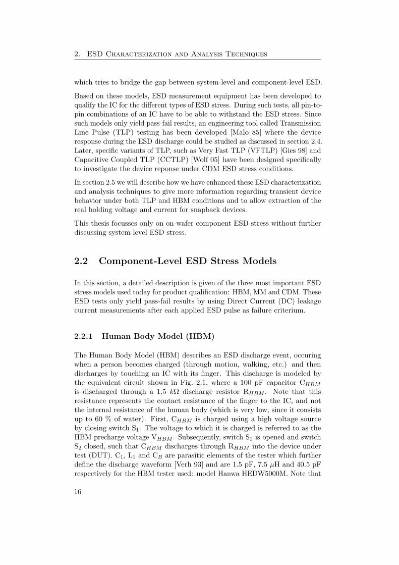
2. ESD Characterization and Analysis Techniques
which tries to bridge the gap between system-level and component-level ESD.
Based on these models, ESD measurement equipment has been developed toqualify the IC for the different types of ESD stress. During such tests, all pin-to-pin combinations of an IC have to be able to withstand the ESD stress. Sincesuch models only yield pass-fail results, an engineering tool called TransmissionLine Pulse (TLP) testing has been developed [Malo 85] where the deviceresponse during the ESD discharge could be studied as discussed in section 2.4.Later, specific variants of TLP, such as Very Fast TLP (VFTLP) [Gies 98] andCapacitive Coupled TLP (CCTLP) [Wolf 05] have been designed specificallyto investigate the device reponse under CDM ESD stress conditions.
In section 2.5 we will describe how we have enhanced these ESD characterizationand analysis techniques to give more information regarding transient devicebehavior under both TLP and HBM conditions and to allow extraction of thereal holding voltage and current for snapback devices.
This thesis focusses only on on-wafer component ESD stress without furtherdiscussing system-level ESD stress.
2.2 Component-Level ESD Stress Models
In this section, a detailed description is given of the three most important ESDstress models used today for product qualification: HBM, MM and CDM. TheseESD tests only yield pass-fail results by using Direct Current (DC) leakagecurrent measurements after each applied ESD pulse as failure criterium.
2.2.1 Human Body Model (HBM)
The Human Body Model (HBM) describes an ESD discharge event, occuringwhen a person becomes charged (through motion, walking, etc.) and thendischarges by touching an IC with its finger. This discharge is modeled bythe equivalent circuit shown in Fig. 2.1, where a 100 pF capacitor CHBM
is discharged through a 1.5 kΩ discharge resistor RHBM . Note that thisresistance represents the contact resistance of the finger to the IC, and notthe internal resistance of the human body (which is very low, since it consistsup to 60 % of water). First, CHBM is charged using a high voltage sourceby closing switch S1. The voltage to which it is charged is referred to as theHBM precharge voltage VHBM . Subsequently, switch S1 is opened and switchS2 closed, such that CHBM discharges through RHBM into the device undertest (DUT). C1, L1 and CB are parasitic elements of the tester which furtherdefine the discharge waveform [Verh 93] and are 1.5 pF, 7.5 µH and 40.5 pFrespectively for the HBM tester used: model Hanwa HEDW5000M. Note that
16
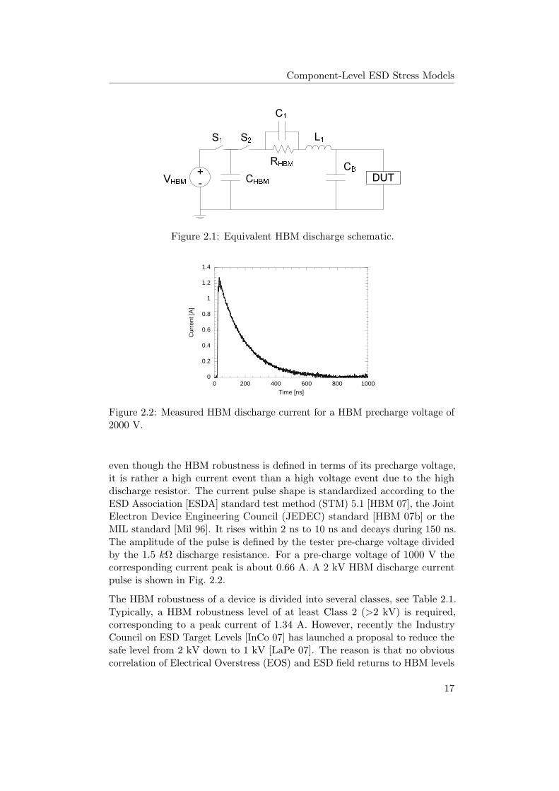
Component-Level ESD Stress Models
+- DUT
RHBMCHBM L1C1
CBS1 S2VHBM
Figure 2.1: Equivalent HBM discharge schematic.
0
0.2
0.4
0.6
0.8
1
1.2
1.4
0 200 400 600 800 1000
Cur
rent
[A]
Time [ns]
Figure 2.2: Measured HBM discharge current for a HBM precharge voltage of2000 V.
even though the HBM robustness is defined in terms of its precharge voltage,it is rather a high current event than a high voltage event due to the highdischarge resistor. The current pulse shape is standardized according to theESD Association [ESDA] standard test method (STM) 5.1 [HBM 07], the JointElectron Device Engineering Council (JEDEC) standard [HBM 07b] or theMIL standard [Mil 96]. It rises within 2 ns to 10 ns and decays during 150 ns.The amplitude of the pulse is defined by the tester pre-charge voltage dividedby the 1.5 kΩ discharge resistance. For a pre-charge voltage of 1000 V thecorresponding current peak is about 0.66 A. A 2 kV HBM discharge currentpulse is shown in Fig. 2.2.
The HBM robustness of a device is divided into several classes, see Table 2.1.Typically, a HBM robustness level of at least Class 2 (>2 kV) is required,corresponding to a peak current of 1.34 A. However, recently the IndustryCouncil on ESD Target Levels [InCo 07] has launched a proposal to reduce thesafe level from 2 kV down to 1 kV [LaPe 07]. The reason is that no obviouscorrelation of Electrical Overstress (EOS) and ESD field returns to HBM levels
17
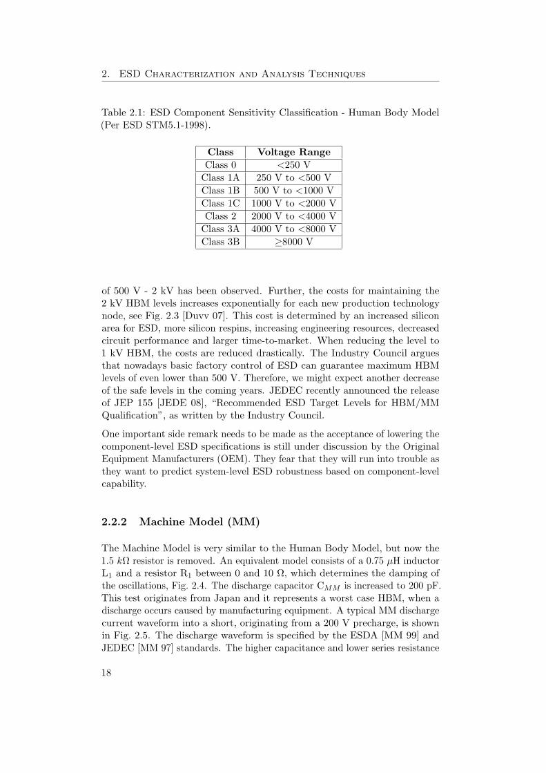
2. ESD Characterization and Analysis Techniques
Table 2.1: ESD Component Sensitivity Classification - Human Body Model(Per ESD STM5.1-1998).
Class Voltage RangeClass 0 <250 V
Class 1A 250 V to <500 VClass 1B 500 V to <1000 VClass 1C 1000 V to <2000 VClass 2 2000 V to <4000 V
Class 3A 4000 V to <8000 VClass 3B ≥8000 V
of 500 V - 2 kV has been observed. Further, the costs for maintaining the2 kV HBM levels increases exponentially for each new production technologynode, see Fig. 2.3 [Duvv 07]. This cost is determined by an increased siliconarea for ESD, more silicon respins, increasing engineering resources, decreasedcircuit performance and larger time-to-market. When reducing the level to1 kV HBM, the costs are reduced drastically. The Industry Council arguesthat nowadays basic factory control of ESD can guarantee maximum HBMlevels of even lower than 500 V. Therefore, we might expect another decreaseof the safe levels in the coming years. JEDEC recently announced the releaseof JEP 155 [JEDE 08], “Recommended ESD Target Levels for HBM/MMQualification”, as written by the Industry Council.
One important side remark needs to be made as the acceptance of lowering thecomponent-level ESD specifications is still under discussion by the OriginalEquipment Manufacturers (OEM). They fear that they will run into trouble asthey want to predict system-level ESD robustness based on component-levelcapability.
2.2.2 Machine Model (MM)
The Machine Model is very similar to the Human Body Model, but now the1.5 kΩ resistor is removed. An equivalent model consists of a 0.75 µH inductorL1 and a resistor R1 between 0 and 10 Ω, which determines the damping ofthe oscillations, Fig. 2.4. The discharge capacitor CMM is increased to 200 pF.This test originates from Japan and it represents a worst case HBM, when adischarge occurs caused by manufacturing equipment. A typical MM dischargecurrent waveform into a short, originating from a 200 V precharge, is shownin Fig. 2.5. The discharge waveform is specified by the ESDA [MM 99] andJEDEC [MM 97] standards. The higher capacitance and lower series resistance
18
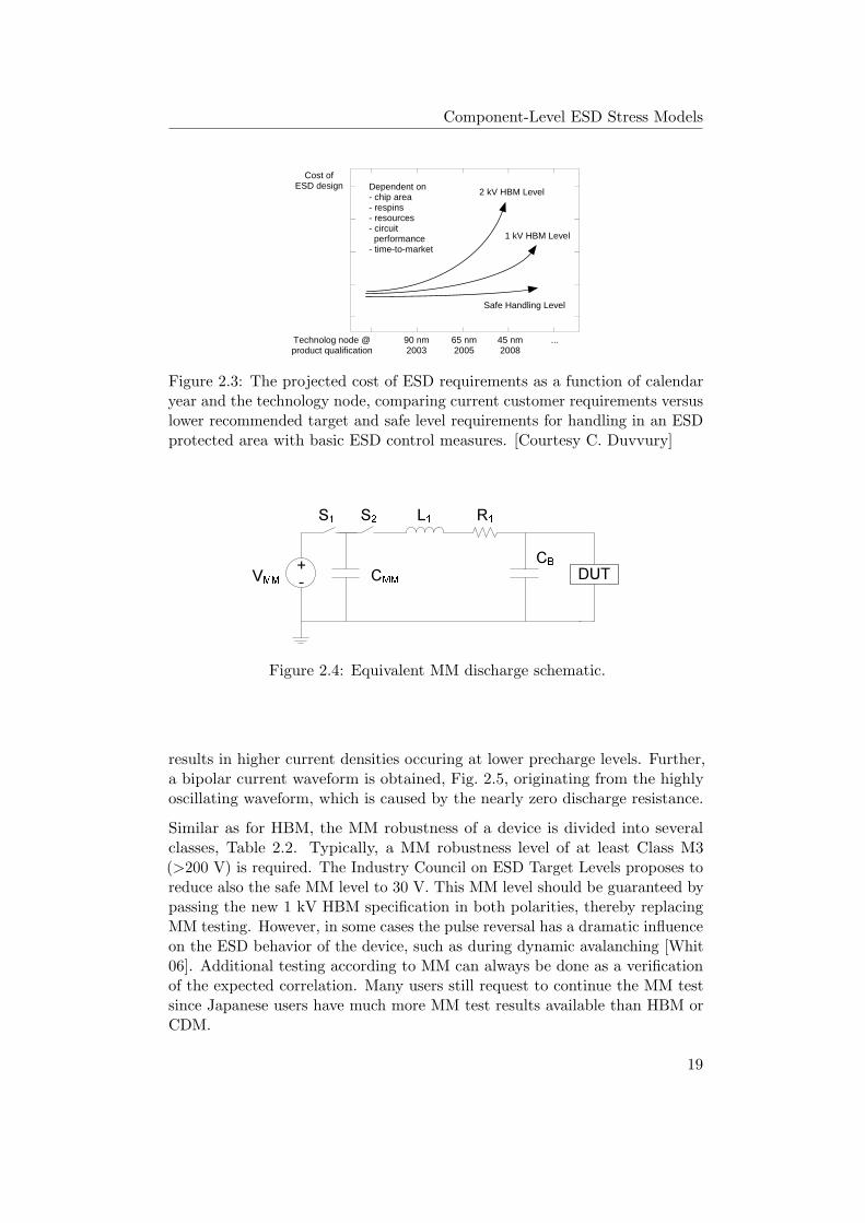
Component-Level ESD Stress Models
Technolog node @product qualification
90 nm2003
65 nm2005
45 nm2008
...
Cost ofESD design
2 kV HBM Level
1 kV HBM Level
Safe Handling Level
Dependent on- chip area- respins- resources- circuit performance- time-to-market
Figure 2.3: The projected cost of ESD requirements as a function of calendaryear and the technology node, comparing current customer requirements versuslower recommended target and safe level requirements for handling in an ESDprotected area with basic ESD control measures. [Courtesy C. Duvvury]
+- DUTCMM CBS1 S2 R1
VMM L1Figure 2.4: Equivalent MM discharge schematic.
results in higher current densities occuring at lower precharge levels. Further,a bipolar current waveform is obtained, Fig. 2.5, originating from the highlyoscillating waveform, which is caused by the nearly zero discharge resistance.
Similar as for HBM, the MM robustness of a device is divided into severalclasses, Table 2.2. Typically, a MM robustness level of at least Class M3(>200 V) is required. The Industry Council on ESD Target Levels proposes toreduce also the safe MM level to 30 V. This MM level should be guaranteed bypassing the new 1 kV HBM specification in both polarities, thereby replacingMM testing. However, in some cases the pulse reversal has a dramatic influenceon the ESD behavior of the device, such as during dynamic avalanching [Whit06]. Additional testing according to MM can always be done as a verificationof the expected correlation. Many users still request to continue the MM testsince Japanese users have much more MM test results available than HBM orCDM.
19
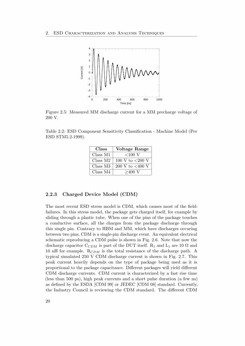
2. ESD Characterization and Analysis Techniques
-4
-3
-2
-1
0
1
2
3
4
0 200 400 600 800 1000
Cur
rent
[A]
Time [ns]
Figure 2.5: Measured MM discharge current for a MM precharge voltage of200 V.
Table 2.2: ESD Component Sensitivity Classification - Machine Model (PerESD STM5.2-1999).
Class Voltage RangeClass M1 <100 VClass M2 100 V to <200 VClass M3 200 V to <400 VClass M4 ≥400 V
2.2.3 Charged Device Model (CDM)
The most recent ESD stress model is CDM, which causes most of the field-failures. In this stress model, the package gets charged itself, for example bysliding through a plastic tube. When one of the pins of the package touchesa conductive surface, all the charges from the package discharge throughthis single pin. Contrary to HBM and MM, which have discharges occuringbetween two pins, CDM is a single-pin discharge event. An equivalent electricalschematic reproducing a CDM pulse is shown in Fig. 2.6. Note that now thedischarge capacitor CCDM is part of the DUT itself. R1 and L1 are 10 Ω and10 nH for example. RCDM is the total resistance of the discharge path. Atypical simulated 250 V CDM discharge current is shown in Fig. 2.7. Thispeak current heavily depends on the type of package being used as it isproportional to the package capacitance. Different packages will yield differentCDM discharge currents. CDM current is characterized by a fast rise time(less than 500 ps), high peak currents and a short pulse duration (a few ns)as defined by the ESDA [CDM 99] or JEDEC [CDM 08] standard. Currently,the Industry Council is reviewing the CDM standard. The different CDM
20
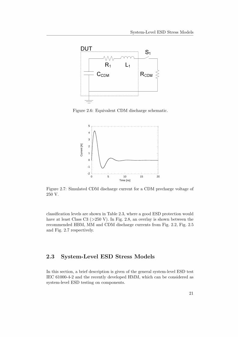
System-Level ESD Stress Models
DUT
R1CCDM L1 S1
RCDMFigure 2.6: Equivalent CDM discharge schematic.
-2
-1
0
1
2
3
4
5
0 5 10 15 20
Cur
rent
[A]
Time [ns]
Figure 2.7: Simulated CDM discharge current for a CDM precharge voltage of250 V.
classification levels are shown in Table 2.3, where a good ESD protection wouldhave at least Class C3 (>250 V). In Fig. 2.8, an overlay is shown between therecommended HBM, MM and CDM discharge currents from Fig. 2.2, Fig. 2.5and Fig. 2.7 respectively.
2.3 System-Level ESD Stress Models
In this section, a brief description is given of the general system-level ESD testIEC 61000-4-2 and the recently developed HMM, which can be considered assystem-level ESD testing on components.
21
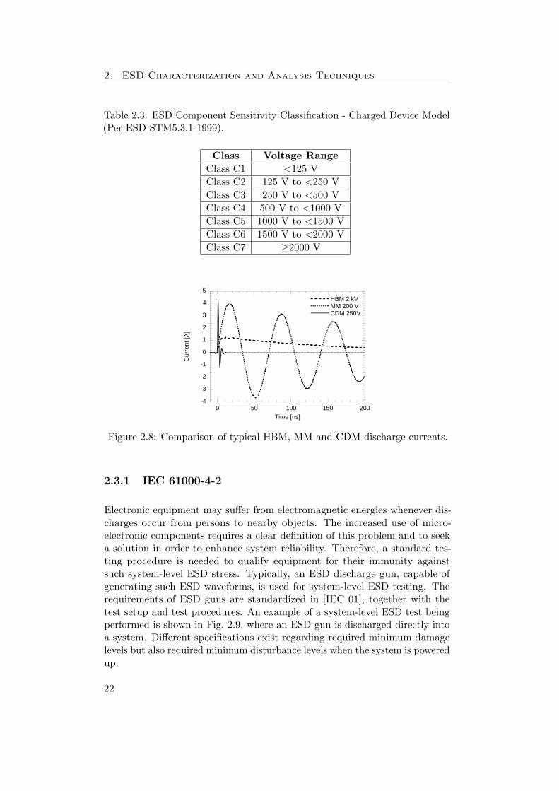
2. ESD Characterization and Analysis Techniques
Table 2.3: ESD Component Sensitivity Classification - Charged Device Model(Per ESD STM5.3.1-1999).
Class Voltage RangeClass C1 <125 VClass C2 125 V to <250 VClass C3 250 V to <500 VClass C4 500 V to <1000 VClass C5 1000 V to <1500 VClass C6 1500 V to <2000 VClass C7 ≥2000 V
-4
-3
-2
-1
0
1
2
3
4
5
0 50 100 150 200
HBM 2 kVMM 200 VCDM 250V
Cur
rent
[A]
Time [ns]
Figure 2.8: Comparison of typical HBM, MM and CDM discharge currents.
2.3.1 IEC 61000-4-2
Electronic equipment may suffer from electromagnetic energies whenever dis-charges occur from persons to nearby objects. The increased use of micro-electronic components requires a clear definition of this problem and to seeka solution in order to enhance system reliability. Therefore, a standard tes-ting procedure is needed to qualify equipment for their immunity againstsuch system-level ESD stress. Typically, an ESD discharge gun, capable ofgenerating such ESD waveforms, is used for system-level ESD testing. Therequirements of ESD guns are standardized in [IEC 01], together with thetest setup and test procedures. An example of a system-level ESD test beingperformed is shown in Fig. 2.9, where an ESD gun is discharged directly intoa system. Different specifications exist regarding required minimum damagelevels but also required minimum disturbance levels when the system is poweredup.
22
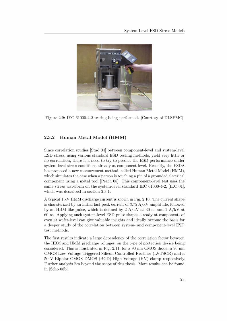
System-Level ESD Stress Models
Figure 2.9: IEC 61000-4-2 testing being performed. [Courtesy of DLSEMC]
2.3.2 Human Metal Model (HMM)
Since correlation studies [Stad 04] between component-level and system-levelESD stress, using various standard ESD testing methods, yield very little orno correlation, there is a need to try to predict the ESD performance undersystem-level stress conditions already at component-level. Recently, the ESDAhas proposed a new measurement method, called Human Metal Model (HMM),which simulates the case when a person is touching a pin of a grounded electricalcomponent using a metal tool [Peach 08]. This component-level test uses thesame stress waveform on the system-level standard IEC 61000-4-2, [IEC 01],which was described in section 2.3.1.
A typical 1 kV HMM discharge current is shown in Fig. 2.10. The current shapeis charaterized by an initial fast peak current of 3.75 A/kV amplitude, followedby an HBM-like pulse, which is defined by 2 A/kV at 30 ns and 1 A/kV at60 ns. Applying such system-level ESD pulse shapes already at component- ofeven at wafer-level can give valuable insights and ideally become the basis fora deeper study of the correlation between system- and component-level ESDtest methods.
The first results indicate a large dependency of the correlation factor betweenthe HBM and HMM precharge voltages, on the type of protection device beingconsidered. This is illustrated in Fig. 2.11, for a 90 nm CMOS diode, a 90 nmCMOS Low Voltage Triggered Silicon Controlled Rectifier (LVTSCR) and a50 V Bipolar CMOS DMOS (BCD) High Voltage (HV) clamp respectively.Further analysis lies beyond the scope of this thesis. More results can be foundin [Scho 08b].
23
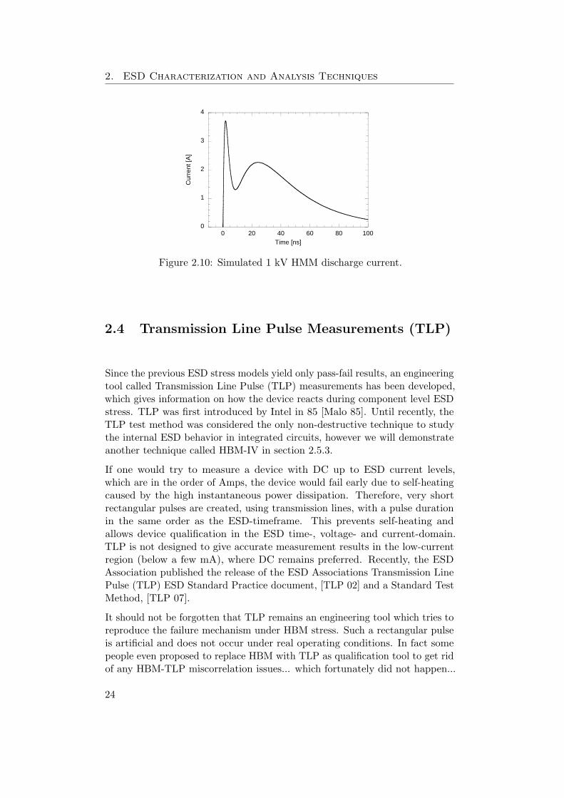
2. ESD Characterization and Analysis Techniques
0
1
2
3
4
0 20 40 60 80 100
Cur
rent
[A]
Time [ns]
Figure 2.10: Simulated 1 kV HMM discharge current.
2.4 Transmission Line Pulse Measurements (TLP)
Since the previous ESD stress models yield only pass-fail results, an engineeringtool called Transmission Line Pulse (TLP) measurements has been developed,which gives information on how the device reacts during component level ESDstress. TLP was first introduced by Intel in 85 [Malo 85]. Until recently, theTLP test method was considered the only non-destructive technique to studythe internal ESD behavior in integrated circuits, however we will demonstrateanother technique called HBM-IV in section 2.5.3.
If one would try to measure a device with DC up to ESD current levels,which are in the order of Amps, the device would fail early due to self-heatingcaused by the high instantaneous power dissipation. Therefore, very shortrectangular pulses are created, using transmission lines, with a pulse durationin the same order as the ESD-timeframe. This prevents self-heating andallows device qualification in the ESD time-, voltage- and current-domain.TLP is not designed to give accurate measurement results in the low-currentregion (below a few mA), where DC remains preferred. Recently, the ESDAssociation published the release of the ESD Associations Transmission LinePulse (TLP) ESD Standard Practice document, [TLP 02] and a Standard TestMethod, [TLP 07].
It should not be forgotten that TLP remains an engineering tool which tries toreproduce the failure mechanism under HBM stress. Such a rectangular pulseis artificial and does not occur under real operating conditions. In fact somepeople even proposed to replace HBM with TLP as qualification tool to get ridof any HBM-TLP miscorrelation issues... which fortunately did not happen...
24
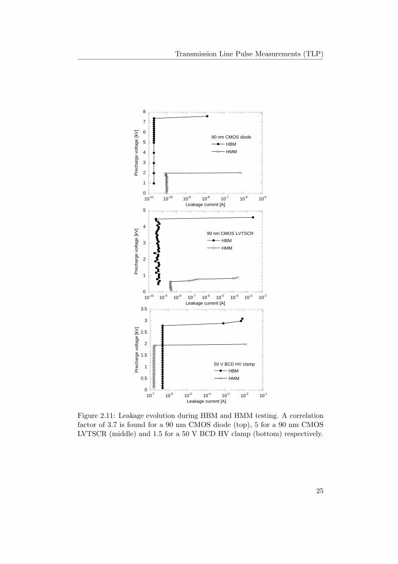
Transmission Line Pulse Measurements (TLP)
0
1
2
3
4
5
6
7
8
10-11 10-10 10-9 10-8 10-7 10-6 10-5
HBM
HMM
Pre
char
ge v
olta
ge [k
V]
Leakage current [A]
90 nm CMOS diode
0
1
2
3
4
5
10-10 10-9 10-8 10-7 10-6 10-5 10-4 10-3 10-2
HBM
HMM
Pre
char
ge v
olta
ge [k
V]
Leakage current [A]
90 nm CMOS LVTSCR
0
0.5
1
1.5
2
2.5
3
3.5
10-7 10-6 10-5 10-4 10-3 10-2 10-1
HBM
HMM
Pre
char
ge v
olta
ge [k
V]
Leakage current [A]
50 V BCD HV clamp
Figure 2.11: Leakage evolution during HBM and HMM testing. A correlationfactor of 3.7 is found for a 90 nm CMOS diode (top), 5 for a 90 nm CMOSLVTSCR (middle) and 1.5 for a 50 V BCD HV clamp (bottom) respectively.
25
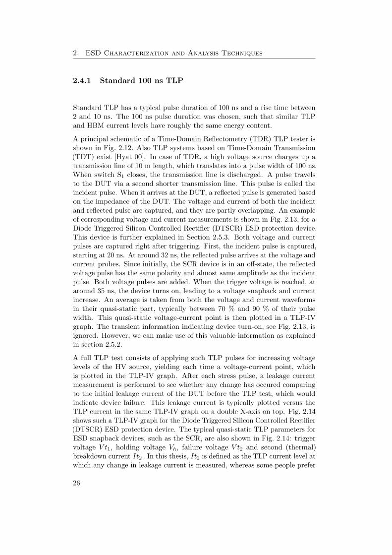
2. ESD Characterization and Analysis Techniques
2.4.1 Standard 100 ns TLP
Standard TLP has a typical pulse duration of 100 ns and a rise time between2 and 10 ns. The 100 ns pulse duration was chosen, such that similar TLPand HBM current levels have roughly the same energy content.
A principal schematic of a Time-Domain Reflectometry (TDR) TLP tester isshown in Fig. 2.12. Also TLP systems based on Time-Domain Transmission(TDT) exist [Hyat 00]. In case of TDR, a high voltage source charges up atransmission line of 10 m length, which translates into a pulse width of 100 ns.When switch S1 closes, the transmission line is discharged. A pulse travelsto the DUT via a second shorter transmission line. This pulse is called theincident pulse. When it arrives at the DUT, a reflected pulse is generated basedon the impedance of the DUT. The voltage and current of both the incidentand reflected pulse are captured, and they are partly overlapping. An exampleof corresponding voltage and current measurements is shown in Fig. 2.13, for aDiode Triggered Silicon Controlled Rectifier (DTSCR) ESD protection device.This device is further explained in Section 2.5.3. Both voltage and currentpulses are captured right after triggering. First, the incident pulse is captured,starting at 20 ns. At around 32 ns, the reflected pulse arrives at the voltage andcurrent probes. Since initially, the SCR device is in an off-state, the reflectedvoltage pulse has the same polarity and almost same amplitude as the incidentpulse. Both voltage pulses are added. When the trigger voltage is reached, ataround 35 ns, the device turns on, leading to a voltage snapback and currentincrease. An average is taken from both the voltage and current waveformsin their quasi-static part, typically between 70 % and 90 % of their pulsewidth. This quasi-static voltage-current point is then plotted in a TLP-IVgraph. The transient information indicating device turn-on, see Fig. 2.13, isignored. However, we can make use of this valuable information as explainedin section 2.5.2.
A full TLP test consists of applying such TLP pulses for increasing voltagelevels of the HV source, yielding each time a voltage-current point, whichis plotted in the TLP-IV graph. After each stress pulse, a leakage currentmeasurement is performed to see whether any change has occured comparingto the initial leakage current of the DUT before the TLP test, which wouldindicate device failure. This leakage current is typically plotted versus theTLP current in the same TLP-IV graph on a double X-axis on top. Fig. 2.14shows such a TLP-IV graph for the Diode Triggered Silicon Controlled Rectifier(DTSCR) ESD protection device. The typical quasi-static TLP parameters forESD snapback devices, such as the SCR, are also shown in Fig. 2.14: triggervoltage V t1, holding voltage Vh, failure voltage V t2 and second (thermal)breakdown current It2. In this thesis, It2 is defined as the TLP current level atwhich any change in leakage current is measured, whereas some people prefer
26
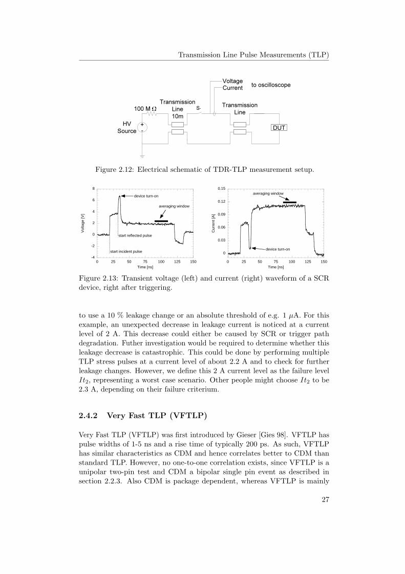
Transmission Line Pulse Measurements (TLP)
+- DUT
TransmissionLine10m
TransmissionLine
VoltageCurrent to oscilloscope
HVSource
100 M S1Figure 2.12: Electrical schematic of TDR-TLP measurement setup.
-4
-2
0
2
4
6
8
0 25 50 75 100 125 150
Vol
tage
[V]
Time [ns]
device turn-on
averaging window
start incident pulse
start reflected pulse
0
0.03
0.06
0.09
0.12
0.15
0 25 50 75 100 125 150
Cur
rent
[A]
Time [ns]
device turn-on
averaging window
Figure 2.13: Transient voltage (left) and current (right) waveform of a SCRdevice, right after triggering.
to use a 10 % leakage change or an absolute threshold of e.g. 1 µA. For thisexample, an unexpected decrease in leakage current is noticed at a currentlevel of 2 A. This decrease could either be caused by SCR or trigger pathdegradation. Futher investigation would be required to determine whether thisleakage decrease is catastrophic. This could be done by performing multipleTLP stress pulses at a current level of about 2.2 A and to check for furtherleakage changes. However, we define this 2 A current level as the failure levelIt2, representing a worst case scenario. Other people might choose It2 to be2.3 A, depending on their failure criterium.
2.4.2 Very Fast TLP (VFTLP)
Very Fast TLP (VFTLP) was first introduced by Gieser [Gies 98]. VFTLP haspulse widths of 1-5 ns and a rise time of typically 200 ps. As such, VFTLPhas similar characteristics as CDM and hence correlates better to CDM thanstandard TLP. However, no one-to-one correlation exists, since VFTLP is aunipolar two-pin test and CDM a bipolar single pin event as described insection 2.2.3. Also CDM is package dependent, whereas VFTLP is mainly
27
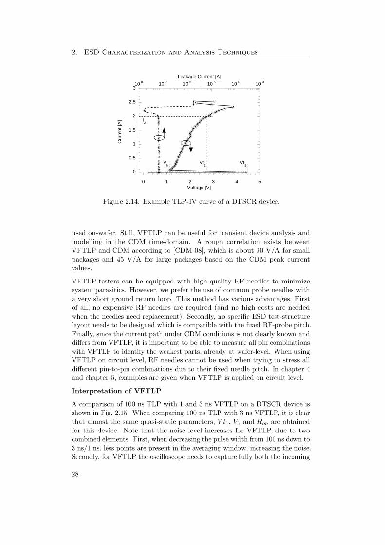
2. ESD Characterization and Analysis Techniques
0
0.5
1
1.5
2
2.5
3
0 1 2 3 4 5
10-8 10-7 10-6 10-5 10-4 10-3
Cur
rent
[A]
Voltage [V]
Leakage Current [A]
It2
Vh
Vt1
Vt2
Figure 2.14: Example TLP-IV curve of a DTSCR device.
used on-wafer. Still, VFTLP can be useful for transient device analysis andmodelling in the CDM time-domain. A rough correlation exists betweenVFTLP and CDM according to [CDM 08], which is about 90 V/A for smallpackages and 45 V/A for large packages based on the CDM peak currentvalues.
VFTLP-testers can be equipped with high-quality RF needles to minimizesystem parasitics. However, we prefer the use of common probe needles witha very short ground return loop. This method has various advantages. Firstof all, no expensive RF needles are required (and no high costs are neededwhen the needles need replacement). Secondly, no specific ESD test-structurelayout needs to be designed which is compatible with the fixed RF-probe pitch.Finally, since the current path under CDM conditions is not clearly known anddiffers from VFTLP, it is important to be able to measure all pin combinationswith VFTLP to identify the weakest parts, already at wafer-level. When usingVFTLP on circuit level, RF needles cannot be used when trying to stress alldifferent pin-to-pin combinations due to their fixed needle pitch. In chapter 4and chapter 5, examples are given when VFTLP is applied on circuit level.
Interpretation of VFTLP
A comparison of 100 ns TLP with 1 and 3 ns VFTLP on a DTSCR device isshown in Fig. 2.15. When comparing 100 ns TLP with 3 ns VFTLP, it is clearthat almost the same quasi-static parameters, V t1, Vh and Ron are obtainedfor this device. Note that the noise level increases for VFTLP, due to twocombined elements. First, when decreasing the pulse width from 100 ns down to3 ns/1 ns, less points are present in the averaging window, increasing the noise.Secondly, for VFTLP the oscilloscope needs to capture fully both the incoming
28
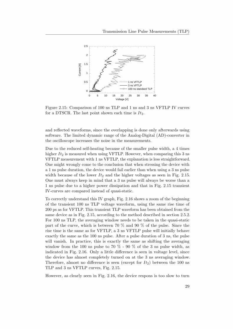
Transmission Line Pulse Measurements (TLP)
0
0.5
1
1.5
2
2.5
0 5 10 15 20 25 30 35 40
1 ns VFTLP3 ns VFTLP100 ns standard TLP
Cur
rent
[A]
Voltage [V]
Figure 2.15: Comparison of 100 ns TLP and 1 ns and 3 ns VFTLP IV curvesfor a DTSCR. The last point shown each time is It2.
and reflected waveforms, since the overlapping is done only afterwards usingsoftware. The limited dynamic range of the Analog-Digital (AD)-converter inthe oscilloscope increases the noise in the measurements.
Due to the reduced self-heating because of the smaller pulse width, a 4 timeshigher It2 is measured when using VFTLP. However, when comparing this 3 nsVFTLP measurement with 1 ns VFTLP, the explanation is less straightforward.One might wrongly come to the conclusion that when stressing the device witha 1 ns pulse duration, the device would fail earlier than when using a 3 ns pulsewidth because of the lower It2 and the higher voltages as seen in Fig. 2.15.One must always keep in mind that a 3 ns pulse will always be worse than a1 ns pulse due to a higher power dissipation and that in Fig. 2.15 transientIV-curves are compared instead of quasi-static.
To correctly understand this IV graph, Fig. 2.16 shows a zoom of the beginningof the transient 100 ns TLP voltage waveform, using the same rise time of200 ps as for VFTLP. This transient TLP waveform has been obtained from thesame device as in Fig. 2.15, according to the method described in section 2.5.2.For 100 ns TLP, the averaging window needs to be taken in the quasi-staticpart of the curve, which is between 70 % and 90 % of the pulse. Since therise time is the same as for VFTLP, a 3 ns VFTLP pulse will initially behaveexactly the same as the 100 ns pulse. After a pulse duration of 3 ns, the pulsewill vanish. In practice, this is exactly the same as shifting the averagingwindow from the 100 ns pulse to 70 % - 90 % of the 3 ns pulse width, asindicated in Fig. 2.16. Only a little difference is seen in voltage level, sincethe device has almost completely turned on at the 3 ns averaging window.Therefore, almost no difference is seen (except for It2) between the 100 nsTLP and 3 ns VFTLP curves, Fig. 2.15.
However, as clearly seen in Fig. 2.16, the device respons is too slow to turn
29
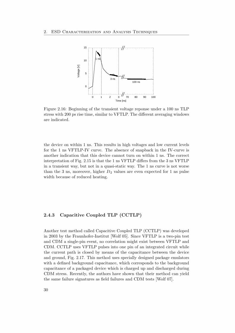
2. ESD Characterization and Analysis Techniques
0
5
10
15
0 1 2 3 70 80 90 100
Vol
tage
[V]
Time [ns]
1 ns
3 ns100 ns
Figure 2.16: Beginning of the transient voltage reponse under a 100 ns TLPstress with 200 ps rise time, similar to VFTLP. The different averaging windowsare indicated.
the device on within 1 ns. This results in high voltages and low current levelsfor the 1 ns VFTLP-IV curve. The absence of snapback in the IV-curve isanother indication that this device cannot turn on within 1 ns. The correctinterpretation of Fig. 2.15 is that the 1 ns VFTLP differs from the 3 ns VFTLPin a transient way, but not in a quasi-static way. The 1 ns curve is not worsethan the 3 ns, moreover, higher It2 values are even expected for 1 ns pulsewidth because of reduced heating.
2.4.3 Capacitive Coupled TLP (CCTLP)
Another test method called Capacitive Coupled TLP (CCTLP) was developedin 2003 by the Fraunhofer-Institut [Wolf 05]. Since VFTLP is a two-pin testand CDM a single-pin event, no correlation might exist between VFTLP andCDM. CCTLP uses VFTLP pulses into one pin of an integrated circuit whilethe current path is closed by means of the capacitance between the deviceand ground, Fig. 2.17. This method uses specially designed package emulatorswith a defined background capacitance, which corresponds to the backgroundcapacitance of a packaged device which is charged up and discharged duringCDM stress. Recently, the authors have shown that their method can yieldthe same failure signatures as field failures and CDM tests [Wolf 07].
30
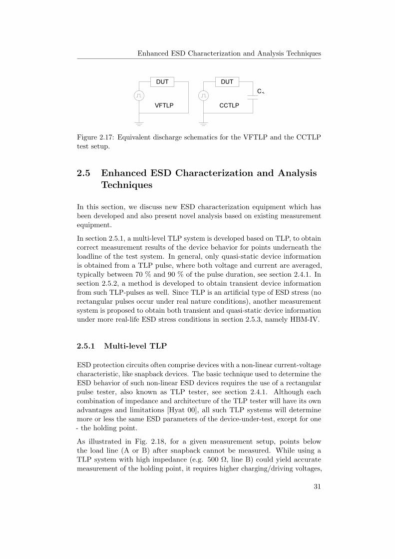
Enhanced ESD Characterization and Analysis Techniques
DUT
VFTLP
DUT
CCTLP
CBFigure 2.17: Equivalent discharge schematics for the VFTLP and the CCTLPtest setup.
2.5 Enhanced ESD Characterization and AnalysisTechniques
In this section, we discuss new ESD characterization equipment which hasbeen developed and also present novel analysis based on existing measurementequipment.
In section 2.5.1, a multi-level TLP system is developed based on TLP, to obtaincorrect measurement results of the device behavior for points underneath theloadline of the test system. In general, only quasi-static device informationis obtained from a TLP pulse, where both voltage and current are averaged,typically between 70 % and 90 % of the pulse duration, see section 2.4.1. Insection 2.5.2, a method is developed to obtain transient device informationfrom such TLP-pulses as well. Since TLP is an artificial type of ESD stress (norectangular pulses occur under real nature conditions), another measurementsystem is proposed to obtain both transient and quasi-static device informationunder more real-life ESD stress conditions in section 2.5.3, namely HBM-IV.
2.5.1 Multi-level TLP
ESD protection circuits often comprise devices with a non-linear current-voltagecharacteristic, like snapback devices. The basic technique used to determine theESD behavior of such non-linear ESD devices requires the use of a rectangularpulse tester, also known as TLP tester, see section 2.4.1. Although eachcombination of impedance and architecture of the TLP tester will have its ownadvantages and limitations [Hyat 00], all such TLP systems will determinemore or less the same ESD parameters of the device-under-test, except for one- the holding point.
As illustrated in Fig. 2.18, for a given measurement setup, points belowthe load line (A or B) after snapback cannot be measured. While using aTLP system with high impedance (e.g. 500 Ω, line B) could yield accuratemeasurement of the holding point, it requires higher charging/driving voltages,
31
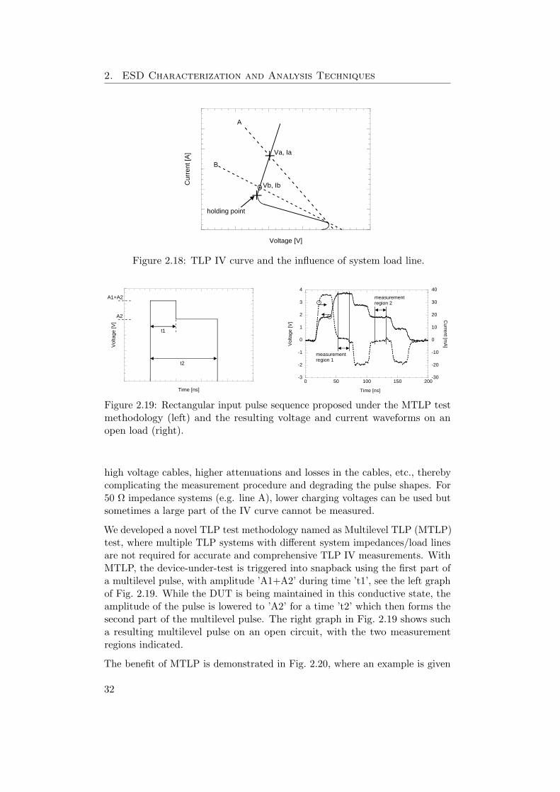
2. ESD Characterization and Analysis Techniques
Cur
rent
[A]
Voltage [V]
holding point
Va, Ia
Vb, Ib
B
A
Figure 2.18: TLP IV curve and the influence of system load line.
Vol
tage
[V]
Time [ns]
A1+A2
A2
t1
t2
-3
-2
-1
0
1
2
3
4
-30
-20
-10
0
10
20
30
40
0 50 100 150 200
Vol
tage
[V]
Current [m
A]
Time [ns]
measurementregion 1
measurementregion 2
Figure 2.19: Rectangular input pulse sequence proposed under the MTLP testmethodology (left) and the resulting voltage and current waveforms on anopen load (right).
high voltage cables, higher attenuations and losses in the cables, etc., therebycomplicating the measurement procedure and degrading the pulse shapes. For50 Ω impedance systems (e.g. line A), lower charging voltages can be used butsometimes a large part of the IV curve cannot be measured.
We developed a novel TLP test methodology named as Multilevel TLP (MTLP)test, where multiple TLP systems with different system impedances/load linesare not required for accurate and comprehensive TLP IV measurements. WithMTLP, the device-under-test is triggered into snapback using the first part ofa multilevel pulse, with amplitude ’A1+A2’ during time ’t1’, see the left graphof Fig. 2.19. While the DUT is being maintained in this conductive state, theamplitude of the pulse is lowered to ’A2’ for a time ’t2’ which then forms thesecond part of the multilevel pulse. The right graph in Fig. 2.19 shows sucha resulting multilevel pulse on an open circuit, with the two measurementregions indicated.
The benefit of MTLP is demonstrated in Fig. 2.20, where an example is given
32
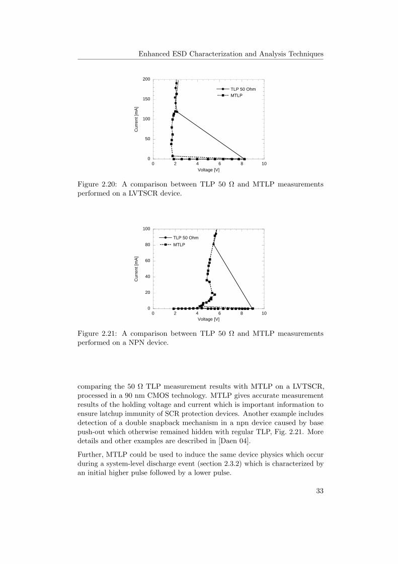
Enhanced ESD Characterization and Analysis Techniques
0
50
100
150
200
0 2 4 6 8 10
TLP 50 OhmMTLP
Cur
rent
[mA
]
Voltage [V]
Figure 2.20: A comparison between TLP 50 Ω and MTLP measurementsperformed on a LVTSCR device.
0
20
40
60
80
100
0 2 4 6 8 10
TLP 50 Ohm
MTLP
Cur
rent
[mA
]
Voltage [V]
Figure 2.21: A comparison between TLP 50 Ω and MTLP measurementsperformed on a NPN device.
comparing the 50 Ω TLP measurement results with MTLP on a LVTSCR,processed in a 90 nm CMOS technology. MTLP gives accurate measurementresults of the holding voltage and current which is important information toensure latchup immunity of SCR protection devices. Another example includesdetection of a double snapback mechanism in a npn device caused by basepush-out which otherwise remained hidden with regular TLP, Fig. 2.21. Moredetails and other examples are described in [Daen 04].
Further, MTLP could be used to induce the same device physics which occurduring a system-level discharge event (section 2.3.2) which is characterized byan initial higher pulse followed by a lower pulse.
33
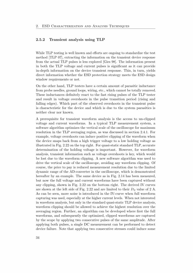
2. ESD Characterization and Analysis Techniques
2.5.2 Transient analysis using TLP
While TLP testing is well known and efforts are ongoing to standardize the testmethod [TLP 07], extracting the information on the transient device responsefrom the actual TLP pulses is less explored [Gies 98]. The information presentin both the TLP voltage and current pulses is significant as it can providein-depth information on the device transient response. This, in turn, yieldsdirect information whether the ESD protection strategy meets the ESD designwindow requirements or not.
On the other hand, TLP testers have a certain amount of parasitic inductancefrom probe needles, ground loops, wiring, etc., which cannot be totally removed.These inductances definitely react to the fast rising pulses of the TLP testerand result in voltage overshoots in the pulse transition period (rising andfalling edges). Which part of the observed overshoots in the transient pulseis characteristic for the device and which is due to the system parasitics isneither clear nor known.
A prerequisite for transient waveform analysis is the access to un-clippedvoltage and current waveforms. In a typical TLP measurement system, asoftware algorithm optimizes the vertical scale of the oscilloscope for maximumresolution in the TLP averaging region, as was discussed in section 2.4.1. Forexample, voltage overshoots can induce positive clipping of the waveform whenthe device snaps back from a high trigger voltage to a low holding voltage asillustrated in Fig. 2.22 on the top right. For quasi-static standard TLP, accuratedetermination of the holding voltage is important. However, for waveformanalysis, transient information such as voltage overshoots is key, which wouldbe lost due to the waveform clipping. A new software algorithm was used todrive the vertical scale of the oscilloscope, avoiding any waveform clipping. Ofcourse, the price to pay is reduced measurement resolution due to the limiteddynamic range of the AD-converter in the oscilloscope, which is demonstratedhereafter by an example. The same device as in Fig. 2.14 has been measured,but now the full voltage and current waveforms have been captured withoutany clipping, shown in Fig. 2.22 on the bottom right. The derived IV curvesare shown at the left side of Fig. 2.22 and are limited to their It2 value of 2 A.As can be seen, more noise is introduced in the IV-curve when full waveformcapturing was used, especially at the higher current levels. When not interestedin waveform analysis, but only in the standard quasi-static TLP device analysis,waveform clipping should be allowed to achieve the highest resolution over theaveraging region. Further, an algorithm can be developed where first the fullwaveforms, and subsequently the optimized, clipped waveforms are capturedby the scope by applying two consecutive pulses of the same amplitude. Afterapplying both pulses, a single DC measurement can be performed to detectdevice failure. Note that applying two consecutive stresses could induce some
34
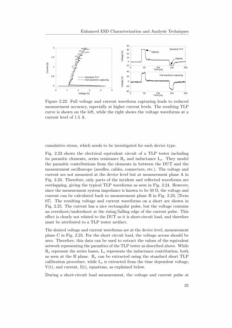
Enhanced ESD Characterization and Analysis Techniques
0
0.5
1
1.5
2
0 1 2 3 4 5
Standard TLPFull waveform capturing
Cur
rent
[A]
Voltage [V]-40
-20
0
20
40
0 50 100 150 200
Vol
tage
[V]
Time [ns]
Full waveform capturing
-10
0
10
20
30
40
0 50 100 150 200
Vol
tage
[V]
Time [ns]
Standard TLPclipping
clipping
Figure 2.22: Full voltage and current waveform capturing leads to reducedmeasurement accuracy, especially at higher current levels. The resulting TLPcurve is shown on the left, while the right shows the voltage waveforms at acurrent level of 1.5 A.
cumulative stress, which needs to be investigated for each device type.
Fig. 2.23 shows the electrical equivalent circuit of a TLP tester includingits parasitic elements, series resistance Rs and inductance Ls. They modelthe parasitic contributions from the elements in between the DUT and themeasurement oscilloscope (needles, cables, connectors, etc.). The voltage andcurrent are not measured at the device level but at measurement plane A inFig. 2.23. Therefore, only parts of the incident and reflected waveforms areoverlapping, giving the typical TLP waveforms as seen in Fig. 2.24. However,since the measurement system impedance is known to be 50 Ω, the voltage andcurrent can be calculated back to measurement plane B in Fig. 2.23, [Trem07]. The resulting voltage and current waveforms on a short are shown inFig. 2.25. The current has a nice rectangular pulse, but the voltage containsan overshoot/undershoot at the rising/falling edge of the current pulse. Thiseffect is clearly not related to the DUT as it is short-circuit load, and thereforemust be attributed to a TLP tester artifact.
The desired voltage and current waveforms are at the device level, measurementplane C in Fig. 2.23. For the short circuit load, the voltage across should bezero. Therefore, this data can be used to extract the values of the equivalentnetwork representing the parasitics of the TLP tester as described above. WhileRs represent the series losses, Ls represents the inductance contribution, bothas seen at the B plane. Rs can be extracted using the standard short TLPcalibration procedure, while Ls is extracted from the time dependent voltage,V(t), and current, I(t), equations, as explained below.
During a short-circuit load measurement, the voltage and current pulse at
35
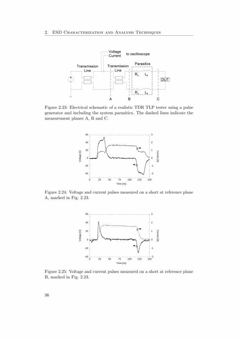
2. ESD Characterization and Analysis Techniques
+-
RsLsLs
DUT
TransmissionLine
TransmissionLine
Parasitics
VoltageCurrent to oscilloscope
A B CRs
Figure 2.23: Electrical schematic of a realistic TDR TLP tester using a pulsegenerator and including the system parasitics. The dashed lines indicate themeasurement planes A, B and C.
-40
-20
0
20
40
60
-2
-1
0
1
2
3
0 25 50 75 100 125 150
Vol
tage
[V] C
urrent [A]
Time [ns]
Figure 2.24: Voltage and current pulses measured on a short at reference planeA, marked in Fig. 2.23.
-40
-20
0
20
40
60
-2
-1
0
1
2
3
0 25 50 75 100 125 150
Vol
tage
[V] C
urrent [A]
Time [ns]
Figure 2.25: Voltage and current pulses measured on a short at reference planeB, marked in Fig. 2.23.
36
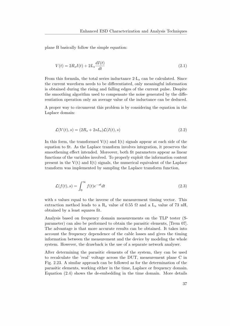
Enhanced ESD Characterization and Analysis Techniques
plane B basically follow the simple equation:
V (t) = 2RsI(t) + 2LsdI(t)dt
(2.1)
From this formula, the total series inductance 2·Ls can be calculated. Sincethe current waveform needs to be differentiated, only meaningful informationis obtained during the rising and falling edges of the current pulse. Despitethe smoothing algorithm used to compensate the noise generated by the diffe-rentiation operation only an average value of the inductance can be deduced.
A proper way to circumvent this problem is by considering the equation in theLaplace domain:
L(V (t), s) = (2Rs + 2sLs)L(I(t), s) (2.2)
In this form, the transformed V(t) and I(t) signals appear at each side of theequation to fit. As the Laplace transform involves integration, it preserves thesmoothening effect intended. Moreover, both fit parameters appear as linearfunctions of the variables involved. To properly exploit the information contentpresent in the V(t) and I(t) signals, the numerical equivalent of the Laplacetransform was implemented by sampling the Laplace transform function,
L(f(t), s) =∫ ∞
0f(t)e−stdt (2.3)
with s values equal to the inverse of the measurement timing vector. Thisextraction method leads to a Rs value of 0.55 Ω and a Ls value of 73 nH,obtained by a least squares fit.
Analysis based on frequency domain measurements on the TLP tester (S-parameter) can also be performed to obtain the parasitic elements, [Trem 07].The advantage is that more accurate results can be obtained. It takes intoaccount the frequency dependence of the cable losses and gives the timinginformation between the measurement and the device by modeling the wholesystem. However, the drawback is the use of a separate network analyser.
After determining the parasitic elements of the system, they can be usedto recalculate the ’real’ voltage across the DUT, measurement plane C inFig. 2.23. A similar approach can be followed as for the determination of theparasitic elements, working either in the time, Laplace or frequency domain.Equation (2.4) shows the de-embedding in the time domain. More details
37
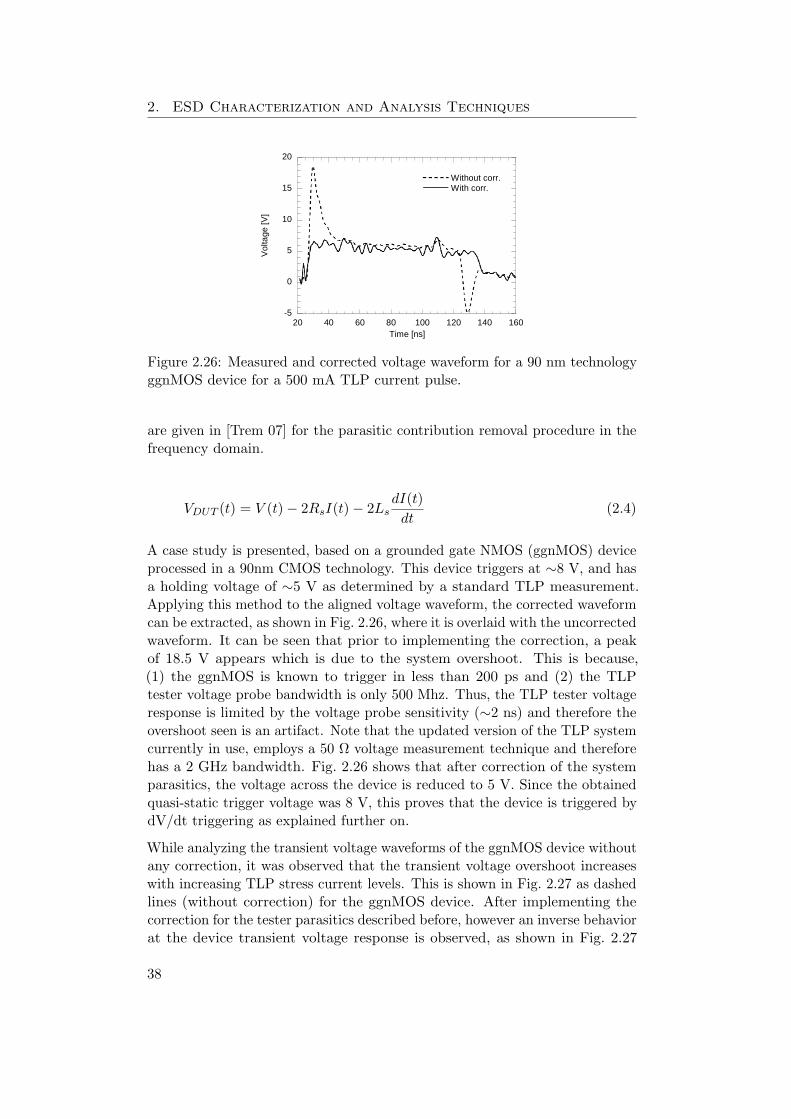
2. ESD Characterization and Analysis Techniques
-5
0
5
10
15
20
20 40 60 80 100 120 140 160
Without corr.With corr.
Vol
tage
[V]
Time [ns]
Figure 2.26: Measured and corrected voltage waveform for a 90 nm technologyggnMOS device for a 500 mA TLP current pulse.
are given in [Trem 07] for the parasitic contribution removal procedure in thefrequency domain.
VDUT (t) = V (t)− 2RsI(t)− 2LsdI(t)dt
(2.4)
A case study is presented, based on a grounded gate NMOS (ggnMOS) deviceprocessed in a 90nm CMOS technology. This device triggers at ∼8 V, and hasa holding voltage of ∼5 V as determined by a standard TLP measurement.Applying this method to the aligned voltage waveform, the corrected waveformcan be extracted, as shown in Fig. 2.26, where it is overlaid with the uncorrectedwaveform. It can be seen that prior to implementing the correction, a peakof 18.5 V appears which is due to the system overshoot. This is because,(1) the ggnMOS is known to trigger in less than 200 ps and (2) the TLPtester voltage probe bandwidth is only 500 Mhz. Thus, the TLP tester voltageresponse is limited by the voltage probe sensitivity (∼2 ns) and therefore theovershoot seen is an artifact. Note that the updated version of the TLP systemcurrently in use, employs a 50 Ω voltage measurement technique and thereforehas a 2 GHz bandwidth. Fig. 2.26 shows that after correction of the systemparasitics, the voltage across the device is reduced to 5 V. Since the obtainedquasi-static trigger voltage was 8 V, this proves that the device is triggered bydV/dt triggering as explained further on.
While analyzing the transient voltage waveforms of the ggnMOS device withoutany correction, it was observed that the transient voltage overshoot increaseswith increasing TLP stress current levels. This is shown in Fig. 2.27 as dashedlines (without correction) for the ggnMOS device. After implementing thecorrection for the tester parasitics described before, however an inverse behaviorat the device transient voltage response is observed, as shown in Fig. 2.27
38
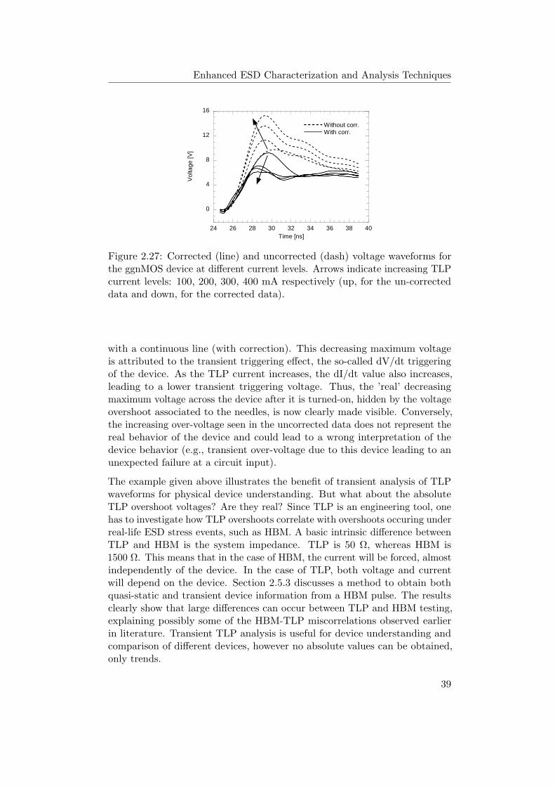
Enhanced ESD Characterization and Analysis Techniques
0
4
8
12
16
24 26 28 30 32 34 36 38 40
Without corr.With corr.
Vol
tage
[V]
Time [ns]
Figure 2.27: Corrected (line) and uncorrected (dash) voltage waveforms forthe ggnMOS device at different current levels. Arrows indicate increasing TLPcurrent levels: 100, 200, 300, 400 mA respectively (up, for the un-correcteddata and down, for the corrected data).
with a continuous line (with correction). This decreasing maximum voltageis attributed to the transient triggering effect, the so-called dV/dt triggeringof the device. As the TLP current increases, the dI/dt value also increases,leading to a lower transient triggering voltage. Thus, the ’real’ decreasingmaximum voltage across the device after it is turned-on, hidden by the voltageovershoot associated to the needles, is now clearly made visible. Conversely,the increasing over-voltage seen in the uncorrected data does not represent thereal behavior of the device and could lead to a wrong interpretation of thedevice behavior (e.g., transient over-voltage due to this device leading to anunexpected failure at a circuit input).
The example given above illustrates the benefit of transient analysis of TLPwaveforms for physical device understanding. But what about the absoluteTLP overshoot voltages? Are they real? Since TLP is an engineering tool, onehas to investigate how TLP overshoots correlate with overshoots occuring underreal-life ESD stress events, such as HBM. A basic intrinsic difference betweenTLP and HBM is the system impedance. TLP is 50 Ω, whereas HBM is1500 Ω. This means that in the case of HBM, the current will be forced, almostindependently of the device. In the case of TLP, both voltage and currentwill depend on the device. Section 2.5.3 discusses a method to obtain bothquasi-static and transient device information from a HBM pulse. The resultsclearly show that large differences can occur between TLP and HBM testing,explaining possibly some of the HBM-TLP miscorrelations observed earlierin literature. Transient TLP analysis is useful for device understanding andcomparison of different devices, however no absolute values can be obtained,only trends.
39
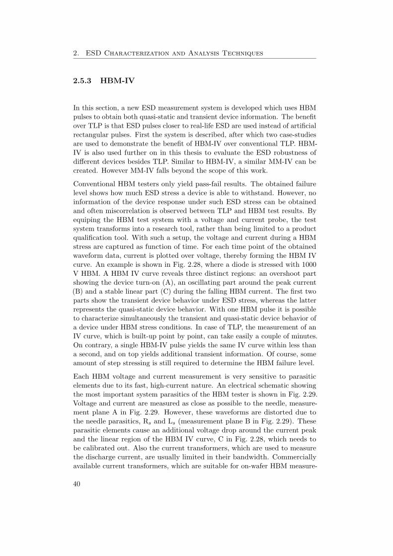
2. ESD Characterization and Analysis Techniques
2.5.3 HBM-IV
In this section, a new ESD measurement system is developed which uses HBMpulses to obtain both quasi-static and transient device information. The benefitover TLP is that ESD pulses closer to real-life ESD are used instead of artificialrectangular pulses. First the system is described, after which two case-studiesare used to demonstrate the benefit of HBM-IV over conventional TLP. HBM-IV is also used further on in this thesis to evaluate the ESD robustness ofdifferent devices besides TLP. Similar to HBM-IV, a similar MM-IV can becreated. However MM-IV falls beyond the scope of this work.
Conventional HBM testers only yield pass-fail results. The obtained failurelevel shows how much ESD stress a device is able to withstand. However, noinformation of the device response under such ESD stress can be obtainedand often miscorrelation is observed between TLP and HBM test results. Byequiping the HBM test system with a voltage and current probe, the testsystem transforms into a research tool, rather than being limited to a productqualification tool. With such a setup, the voltage and current during a HBMstress are captured as function of time. For each time point of the obtainedwaveform data, current is plotted over voltage, thereby forming the HBM IVcurve. An example is shown in Fig. 2.28, where a diode is stressed with 1000V HBM. A HBM IV curve reveals three distinct regions: an overshoot partshowing the device turn-on (A), an oscillating part around the peak current(B) and a stable linear part (C) during the falling HBM current. The first twoparts show the transient device behavior under ESD stress, whereas the latterrepresents the quasi-static device behavior. With one HBM pulse it is possibleto characterize simultaneously the transient and quasi-static device behavior ofa device under HBM stress conditions. In case of TLP, the measurement of anIV curve, which is built-up point by point, can take easily a couple of minutes.On contrary, a single HBM-IV pulse yields the same IV curve within less thana second, and on top yields additional transient information. Of course, someamount of step stressing is still required to determine the HBM failure level.
Each HBM voltage and current measurement is very sensitive to parasiticelements due to its fast, high-current nature. An electrical schematic showingthe most important system parasitics of the HBM tester is shown in Fig. 2.29.Voltage and current are measured as close as possible to the needle, measure-ment plane A in Fig. 2.29. However, these waveforms are distorted due tothe needle parasitics, Rs and Ls (measurement plane B in Fig. 2.29). Theseparasitic elements cause an additional voltage drop around the current peakand the linear region of the HBM IV curve, C in Fig. 2.28, which needs tobe calibrated out. Also the current transformers, which are used to measurethe discharge current, are usually limited in their bandwidth. Commerciallyavailable current transformers, which are suitable for on-wafer HBM measure-
40
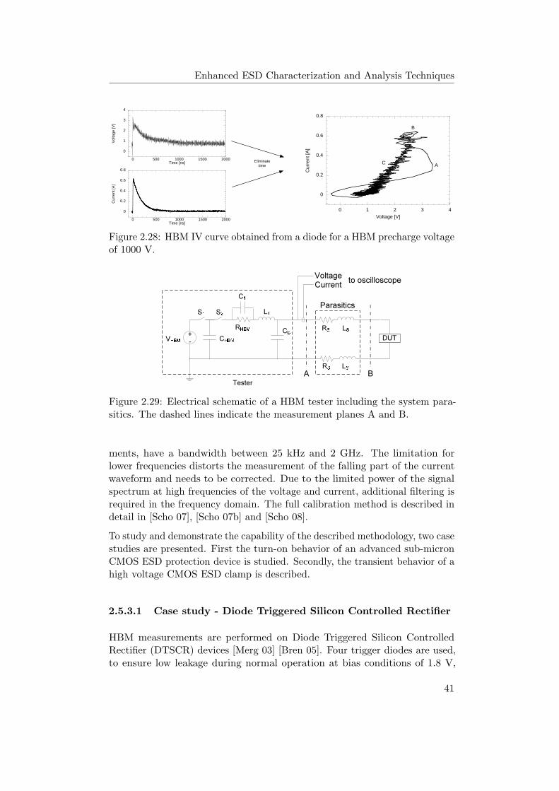
Enhanced ESD Characterization and Analysis Techniques
0
0.2
0.4
0.6
0.8
0 500 1000 1500 2000
Cur
rent
[A]
Time [ns]
0
1
2
3
4
0 500 1000 1500 2000
Vol
tage
[V]
Time [ns] Eliminatetime
0
0.2
0.4
0.6
0.8
0 1 2 3 4
Cur
rent
[A]
Voltage [V]
A
B
C
Figure 2.28: HBM IV curve obtained from a diode for a HBM precharge voltageof 1000 V.
+-
RSLSLS
DUTRHBM
CHBM L1C1Tester
CB Parasitics
A BRS
VoltageCurrent to oscilloscope
S1 S2VHBM
Figure 2.29: Electrical schematic of a HBM tester including the system para-sitics. The dashed lines indicate the measurement planes A and B.
ments, have a bandwidth between 25 kHz and 2 GHz. The limitation forlower frequencies distorts the measurement of the falling part of the currentwaveform and needs to be corrected. Due to the limited power of the signalspectrum at high frequencies of the voltage and current, additional filtering isrequired in the frequency domain. The full calibration method is described indetail in [Scho 07], [Scho 07b] and [Scho 08].
To study and demonstrate the capability of the described methodology, two casestudies are presented. First the turn-on behavior of an advanced sub-micronCMOS ESD protection device is studied. Secondly, the transient behavior of ahigh voltage CMOS ESD clamp is described.
2.5.3.1 Case study - Diode Triggered Silicon Controlled Rectifier
HBM measurements are performed on Diode Triggered Silicon ControlledRectifier (DTSCR) devices [Merg 03] [Bren 05]. Four trigger diodes are used,to ensure low leakage during normal operation at bias conditions of 1.8 V,
41
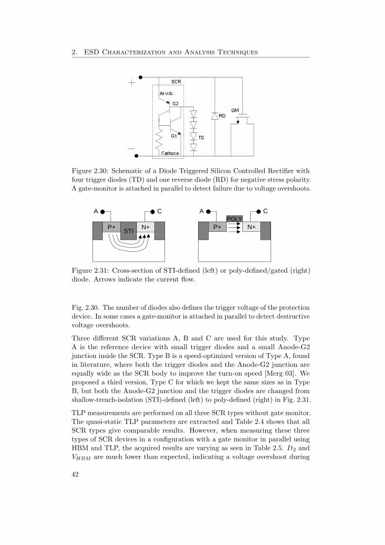
2. ESD Characterization and Analysis TechniquesSCRTD RD GMAnode
CathodeG1G2Figure 2.30: Schematic of a Diode Triggered Silicon Controlled Rectifier withfour trigger diodes (TD) and one reverse diode (RD) for negative stress polarity.A gate-monitor is attached in parallel to detect failure due to voltage overshoots.
STIN+P+
A CPOLY
N+P+
A C
Figure 2.31: Cross-section of STI-defined (left) or poly-defined/gated (right)diode. Arrows indicate the current flow.
Fig. 2.30. The number of diodes also defines the trigger voltage of the protectiondevice. In some cases a gate-monitor is attached in parallel to detect destructivevoltage overshoots.
Three different SCR variations A, B and C are used for this study. TypeA is the reference device with small trigger diodes and a small Anode-G2junction inside the SCR. Type B is a speed-optimized version of Type A, foundin literature, where both the trigger diodes and the Anode-G2 junction areequally wide as the SCR body to improve the turn-on speed [Merg 03]. Weproposed a third version, Type C for which we kept the same sizes as in TypeB, but both the Anode-G2 junction and the trigger diodes are changed fromshallow-trench-isolation (STI)-defined (left) to poly-defined (right) in Fig. 2.31.
TLP measurements are performed on all three SCR types without gate monitor.The quasi-static TLP parameters are extracted and Table 2.4 shows that allSCR types give comparable results. However, when measuring these threetypes of SCR devices in a configuration with a gate monitor in parallel usingHBM and TLP, the acquired results are varying as seen in Table 2.5. It2 andVHBM are much lower than expected, indicating a voltage overshoot during
42
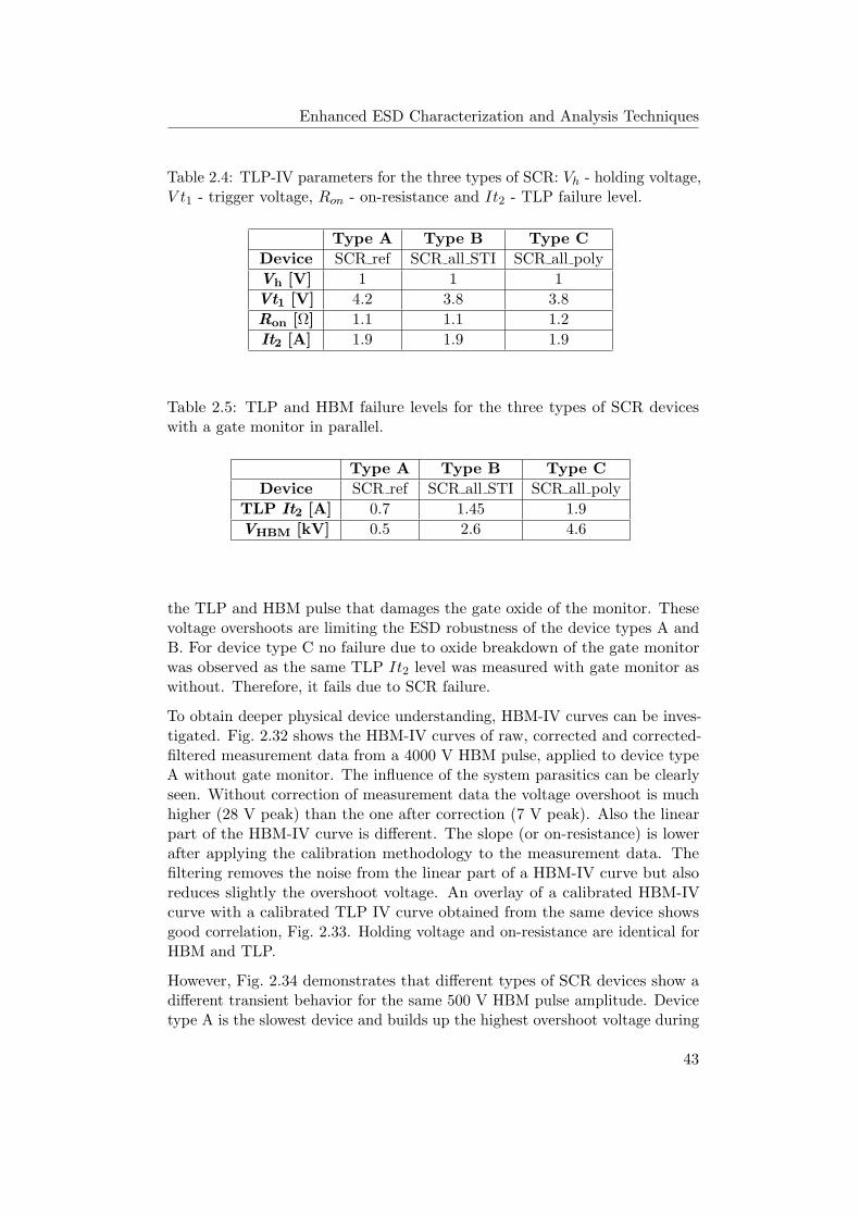
Enhanced ESD Characterization and Analysis Techniques
Table 2.4: TLP-IV parameters for the three types of SCR: Vh - holding voltage,V t1 - trigger voltage, Ron - on-resistance and It2 - TLP failure level.
Type A Type B Type CDevice SCR ref SCR all STI SCR all polyVh [V] 1 1 1Vt1 [V] 4.2 3.8 3.8Ron [Ω] 1.1 1.1 1.2It2 [A] 1.9 1.9 1.9
Table 2.5: TLP and HBM failure levels for the three types of SCR deviceswith a gate monitor in parallel.
Type A Type B Type CDevice SCR ref SCR all STI SCR all poly
TLP It2 [A] 0.7 1.45 1.9VHBM [kV] 0.5 2.6 4.6
the TLP and HBM pulse that damages the gate oxide of the monitor. Thesevoltage overshoots are limiting the ESD robustness of the device types A andB. For device type C no failure due to oxide breakdown of the gate monitorwas observed as the same TLP It2 level was measured with gate monitor aswithout. Therefore, it fails due to SCR failure.
To obtain deeper physical device understanding, HBM-IV curves can be inves-tigated. Fig. 2.32 shows the HBM-IV curves of raw, corrected and corrected-filtered measurement data from a 4000 V HBM pulse, applied to device typeA without gate monitor. The influence of the system parasitics can be clearlyseen. Without correction of measurement data the voltage overshoot is muchhigher (28 V peak) than the one after correction (7 V peak). Also the linearpart of the HBM-IV curve is different. The slope (or on-resistance) is lowerafter applying the calibration methodology to the measurement data. Thefiltering removes the noise from the linear part of a HBM-IV curve but alsoreduces slightly the overshoot voltage. An overlay of a calibrated HBM-IVcurve with a calibrated TLP IV curve obtained from the same device showsgood correlation, Fig. 2.33. Holding voltage and on-resistance are identical forHBM and TLP.
However, Fig. 2.34 demonstrates that different types of SCR devices show adifferent transient behavior for the same 500 V HBM pulse amplitude. Devicetype A is the slowest device and builds up the highest overshoot voltage during
43
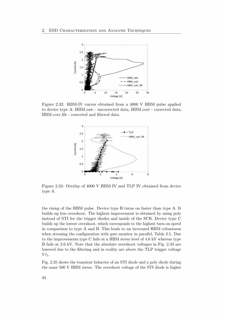
2. ESD Characterization and Analysis Techniques
0
0.5
1
1.5
2
2.5
3
0 5 10 15 20 25 30
HBM_raw
HBM_corr
HBM_corr_filt
Cur
rent
[A]
Voltage [V]
Figure 2.32: HBM-IV curves obtained from a 4000 V HBM pulse appliedto device type A: HBM raw - uncorrected data, HBM corr - corrected data,HBM corr filt - corrected and filtered data.
0
0.5
1
1.5
2
2.5
3
0 2 4 6 8
TLP
HBM_corr_filt
Cur
rent
[A]
Voltage [V]
Figure 2.33: Overlay of 4000 V HBM-IV and TLP IV obtained from devicetype A.
the rising of the HBM pulse. Device type B turns on faster than type A. Itbuilds up less overshoot. The highest improvement is obtained by using polyinstead of STI for the trigger diodes and inside of the SCR. Device type Cbuilds up the lowest overshoot, which corresponds to the highest turn-on speedin comparison to type A and B. This leads to an increased HBM robustnesswhen stressing the configuration with gate monitor in parallel, Table 2.5. Dueto the improvements type C fails at a HBM stress level of 4.6 kV whereas typeB fails at 2.6 kV. Note that the absolute overshoot voltages in Fig. 2.34 arelowered due to the filtering and in reality are above the TLP trigger voltageV t1.
Fig. 2.35 shows the transient behavior of an STI diode and a poly diode duringthe same 500 V HBM stress. The overshoot voltage of the STI diode is higher
44
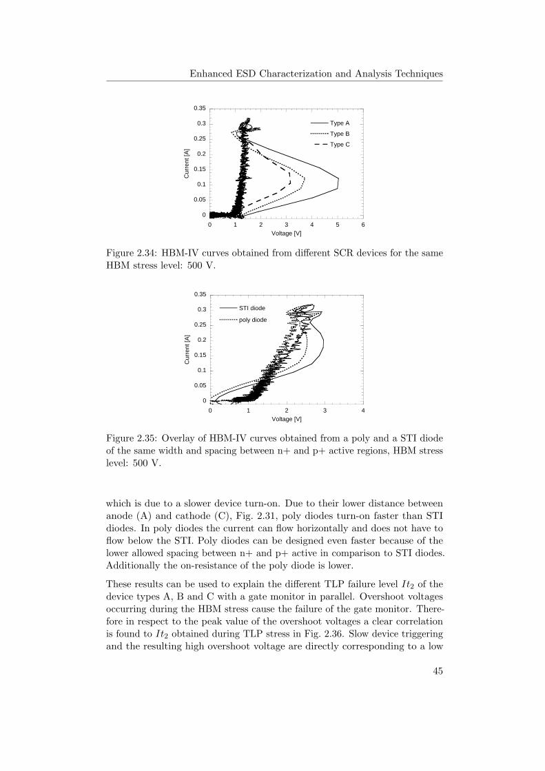
Enhanced ESD Characterization and Analysis Techniques
0
0.05
0.1
0.15
0.2
0.25
0.3
0.35
0 1 2 3 4 5 6
Type A
Type B
Type C
Cur
rent
[A]
Voltage [V]
Figure 2.34: HBM-IV curves obtained from different SCR devices for the sameHBM stress level: 500 V.
0
0.05
0.1
0.15
0.2
0.25
0.3
0.35
0 1 2 3 4
STI diode
poly diode
Cur
rent
[A]
Voltage [V]
Figure 2.35: Overlay of HBM-IV curves obtained from a poly and a STI diodeof the same width and spacing between n+ and p+ active regions, HBM stresslevel: 500 V.
which is due to a slower device turn-on. Due to their lower distance betweenanode (A) and cathode (C), Fig. 2.31, poly diodes turn-on faster than STIdiodes. In poly diodes the current can flow horizontally and does not have toflow below the STI. Poly diodes can be designed even faster because of thelower allowed spacing between n+ and p+ active in comparison to STI diodes.Additionally the on-resistance of the poly diode is lower.
These results can be used to explain the different TLP failure level It2 of thedevice types A, B and C with a gate monitor in parallel. Overshoot voltagesoccurring during the HBM stress cause the failure of the gate monitor. There-fore in respect to the peak value of the overshoot voltages a clear correlationis found to It2 obtained during TLP stress in Fig. 2.36. Slow device triggeringand the resulting high overshoot voltage are directly corresponding to a low
45
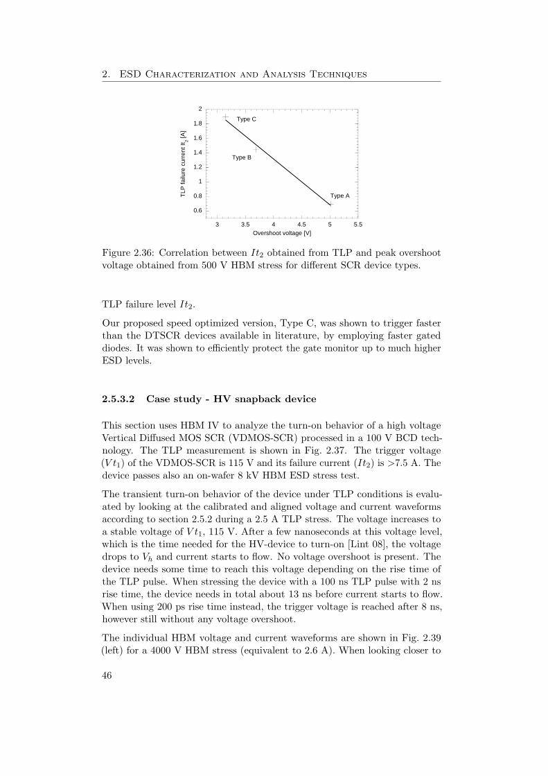
2. ESD Characterization and Analysis Techniques
0.6
0.8
1
1.2
1.4
1.6
1.8
2
3 3.5 4 4.5 5 5.5
TLP
failu
re c
urre
nt It
2 [A]
Overshoot voltage [V]
Type C
Type B
Type A
Figure 2.36: Correlation between It2 obtained from TLP and peak overshootvoltage obtained from 500 V HBM stress for different SCR device types.
TLP failure level It2.
Our proposed speed optimized version, Type C, was shown to trigger fasterthan the DTSCR devices available in literature, by employing faster gateddiodes. It was shown to efficiently protect the gate monitor up to much higherESD levels.
2.5.3.2 Case study - HV snapback device
This section uses HBM IV to analyze the turn-on behavior of a high voltageVertical Diffused MOS SCR (VDMOS-SCR) processed in a 100 V BCD tech-nology. The TLP measurement is shown in Fig. 2.37. The trigger voltage(V t1) of the VDMOS-SCR is 115 V and its failure current (It2) is >7.5 A. Thedevice passes also an on-wafer 8 kV HBM ESD stress test.
The transient turn-on behavior of the device under TLP conditions is evalu-ated by looking at the calibrated and aligned voltage and current waveformsaccording to section 2.5.2 during a 2.5 A TLP stress. The voltage increases toa stable voltage of V t1, 115 V. After a few nanoseconds at this voltage level,which is the time needed for the HV-device to turn-on [Lint 08], the voltagedrops to Vh and current starts to flow. No voltage overshoot is present. Thedevice needs some time to reach this voltage depending on the rise time ofthe TLP pulse. When stressing the device with a 100 ns TLP pulse with 2 nsrise time, the device needs in total about 13 ns before current starts to flow.When using 200 ps rise time instead, the trigger voltage is reached after 8 ns,however still without any voltage overshoot.
The individual HBM voltage and current waveforms are shown in Fig. 2.39(left) for a 4000 V HBM stress (equivalent to 2.6 A). When looking closer to
46
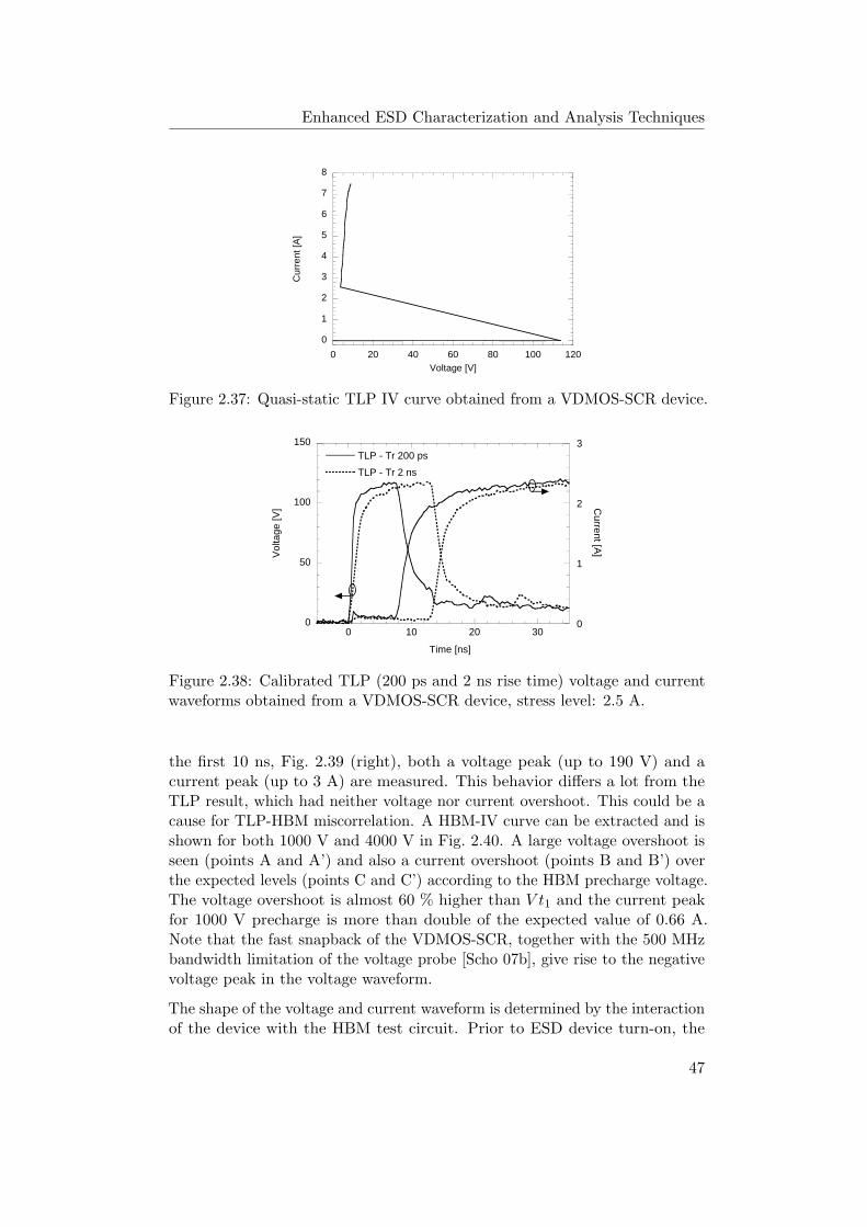
Enhanced ESD Characterization and Analysis Techniques
0
1
2
3
4
5
6
7
8
0 20 40 60 80 100 120
Cur
rent
[A]
Voltage [V]
Figure 2.37: Quasi-static TLP IV curve obtained from a VDMOS-SCR device.
0
50
100
150
0 10 20 30
TLP - Tr 200 ps
TLP - Tr 2 ns
0
1
2
3
Vol
tage
[V]
Time [ns]
Current [A
]
Figure 2.38: Calibrated TLP (200 ps and 2 ns rise time) voltage and currentwaveforms obtained from a VDMOS-SCR device, stress level: 2.5 A.
the first 10 ns, Fig. 2.39 (right), both a voltage peak (up to 190 V) and acurrent peak (up to 3 A) are measured. This behavior differs a lot from theTLP result, which had neither voltage nor current overshoot. This could be acause for TLP-HBM miscorrelation. A HBM-IV curve can be extracted and isshown for both 1000 V and 4000 V in Fig. 2.40. A large voltage overshoot isseen (points A and A’) and also a current overshoot (points B and B’) overthe expected levels (points C and C’) according to the HBM precharge voltage.The voltage overshoot is almost 60 % higher than V t1 and the current peakfor 1000 V precharge is more than double of the expected value of 0.66 A.Note that the fast snapback of the VDMOS-SCR, together with the 500 MHzbandwidth limitation of the voltage probe [Scho 07b], give rise to the negativevoltage peak in the voltage waveform.
The shape of the voltage and current waveform is determined by the interactionof the device with the HBM test circuit. Prior to ESD device turn-on, the
47
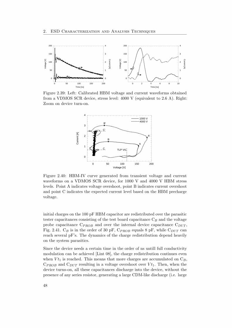
2. ESD Characterization and Analysis Techniques
0
50
100
150
200
0
1
2
3
4
0 50 100 150 200
Vol
tage
[V] C
urrent [A]
Time [ns]
0
50
100
150
200
0
1
2
3
4
0 2 4 6 8 10
Vol
tage
[V] C
urrent [A]
Time [ns]
Figure 2.39: Left: Calibrated HBM voltage and current waveforms obtainedfrom a VDMOS SCR device, stress level: 4000 V (equivalent to 2.6 A). Right:Zoom on device turn-on.
0
1
2
3
4
0 50 100 150 200
4000 V1000 V
Cur
rent
[A]
Voltage [V]
A'
B'
A
B
C TLP Vt1
C'
Figure 2.40: HBM-IV curve generated from transient voltage and currentwaveforms on a VDMOS SCR device, for 1000 V and 4000 V HBM stresslevels. Point A indicates voltage overshoot, point B indicates current overshootand point C indicates the expected current level based on the HBM prechargevoltage.
initial charges on the 100 pF HBM capacitor are redistributed over the parasitictester capacitances consisting of the test board capacitance CB and the voltageprobe capacitance CPROB and over the internal device capacitance CDUT ,Fig. 2.41. CB is in the order of 30 pF, CPROB equals 8 pF, while CDUT canreach several pF’s. The dynamics of the charge redistribution depend heavilyon the system parasitics.
Since the device needs a certain time in the order of ns untill full conductivitymodulation can be achieved [Lint 08], the charge redistribution continues evenwhen V t1 is reached. This means that more charges are accumulated on CB,CPROB and CDUT resulting in a voltage overshoot over V t1. Then, when thedevice turns-on, all these capacitances discharge into the device, without thepresence of any series resistor, generating a large CDM-like discharge (i.e. large
48
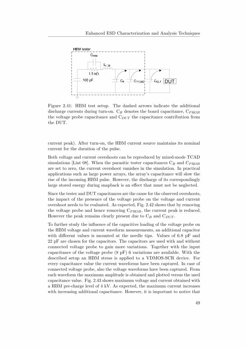
Enhanced ESD Characterization and Analysis Techniques
DUT1.5 k100 pF CBCHBM LHBM CPROBE CDUT
HBM tester
Figure 2.41: HBM test setup. The dashed arrows indicate the additionaldischarge currents during turn-on. CB denotes the board capacitance, CPROB
the voltage probe capacitance and CDUT the capacitance contribution fromthe DUT.
current peak). After turn-on, the HBM current source maintains its nominalcurrent for the duration of the pulse.
Both voltage and current overshoots can be reproduced by mixed-mode TCADsimulations [Lint 08]. When the parasitic tester capacitances CB and CPROB
are set to zero, the current overshoot vanishes in the simulation. In practicalapplications such as large power arrays, the array’s capacitance will slow therise of the incoming HBM pulse. However, the discharge of its correspondinglylarge stored energy during snapback is an effect that must not be neglected.
Since the tester and DUT capacitances are the cause for the observed overshoots,the impact of the presence of the voltage probe on the voltage and currentovershoot needs to be evaluated. As expected, Fig. 2.42 shows that by removingthe voltage probe and hence removing CPROB, the current peak is reduced.However the peak remains clearly present due to CB and CDUT .
To further study the influence of the capacitive loading of the voltage probe onthe HBM voltage and current waveform measurements, an additional capacitorwith different values is mounted at the needle tips. Values of 6.8 pF and22 pF are chosen for the capacitors. The capacitors are used with and withoutconnected voltage probe to gain more variations. Together with the inputcapacitance of the voltage probe (8 pF) 6 variations are available. With thedescribed setup an HBM stress is applied to a VDMOS-SCR device. Forevery capacitance value the current waveforms have been captured. In case ofconnected voltage probe, also the voltage waveforms have been captured. Fromeach waveform the maximum amplitude is obtained and plotted versus the usedcapacitance value. Fig. 2.43 shows maximum voltage and current obtained witha HBM pre-charge level of 4 kV. As expected, the maximum current increaseswith increasing additional capacitance. However, it is important to notice that
49
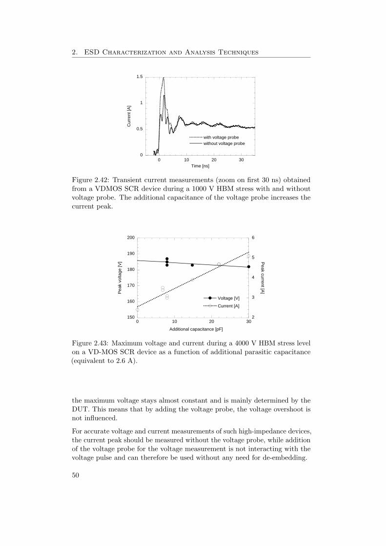
2. ESD Characterization and Analysis Techniques
0
0.5
1
1.5
0 10 20 30
with voltage probewithout voltage probe
Cur
rent
[A]
Time [ns]
Figure 2.42: Transient current measurements (zoom on first 30 ns) obtainedfrom a VDMOS SCR device during a 1000 V HBM stress with and withoutvoltage probe. The additional capacitance of the voltage probe increases thecurrent peak.
150
160
170
180
190
200
2
3
4
5
6
0 10 20 30
Voltage [V]
Current [A]
Pea
k vo
ltage
[V] P
eak current [A]
Additional capacitance [pF]
Figure 2.43: Maximum voltage and current during a 4000 V HBM stress levelon a VD-MOS SCR device as a function of additional parasitic capacitance(equivalent to 2.6 A).
the maximum voltage stays almost constant and is mainly determined by theDUT. This means that by adding the voltage probe, the voltage overshoot isnot influenced.
For accurate voltage and current measurements of such high-impedance devices,the current peak should be measured without the voltage probe, while additionof the voltage probe for the voltage measurement is not interacting with thevoltage pulse and can therefore be used without any need for de-embedding.
50
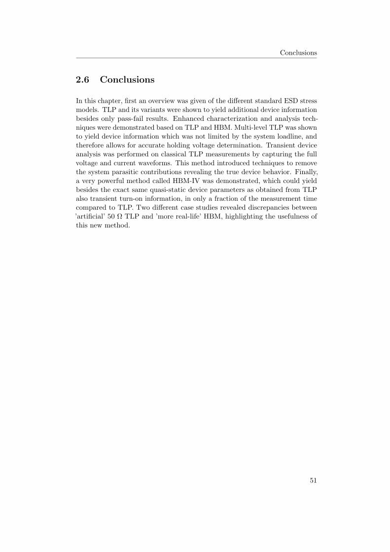
Conclusions
2.6 Conclusions
In this chapter, first an overview was given of the different standard ESD stressmodels. TLP and its variants were shown to yield additional device informationbesides only pass-fail results. Enhanced characterization and analysis tech-niques were demonstrated based on TLP and HBM. Multi-level TLP was shownto yield device information which was not limited by the system loadline, andtherefore allows for accurate holding voltage determination. Transient deviceanalysis was performed on classical TLP measurements by capturing the fullvoltage and current waveforms. This method introduced techniques to removethe system parasitic contributions revealing the true device behavior. Finally,a very powerful method called HBM-IV was demonstrated, which could yieldbesides the exact same quasi-static device parameters as obtained from TLPalso transient turn-on information, in only a fraction of the measurement timecompared to TLP. Two different case studies revealed discrepancies between’artificial’ 50 Ω TLP and ’more real-life’ HBM, highlighting the usefulness ofthis new method.
51

Chapter 3
ESD Protection in FinFETTechnology
Despite a small silicon volume to dissipate the heat from ESD discharges, it isdemonstrated that FinFET devices can have reasonably good ESD robustness,depending strongly on layout and process parameters. Different normalizationtechniques are required for correct data interpretation. A design methodologyis needed to determine the optimal device solution for a given set of ESD andfunctional constraints.
3.1 Introduction
The reliability of sub-micrometer devices and circuits is a major issue thatdetermines both their manufacturability and application lifetime. Designfor reliability should be implemented during technology, device and circuitdevelopment to avoid undesirable product development cycles and costly yieldloss and field failures. As CMOS keeps scaling down, new technology optionsarise and their ESD robustness should be preferably considered in the earlytechnology development phase as these technology evolutions might lead to a’drastic’ reduction in ESD robustness as it has been the case in the past whennew technology features, such as silicides and Lightly Doped Drain (LDD),were introduced [Amer 02].
According to the International Technology Roadmap for Semiconductors (ITRS)2007 [ITRS], the physical gate length of a transistor will reach the size of9 nm in 2016. Even if lithography and etching techniques can provide thesedimensions, bulk CMOS will run into a number of Short Channel Effects (SCE)associated with transistor scaling, such as Drain-Induced Barrier Lowering(DIBL), punchthrough and velocity saturation. New devices start to arise,
3. ESD Protection in FinFET Technology
out of which multi-gate MOSFET devices show promising performances. TheFinFET transistor is the most widely studied multi-gate architecture fortechnology-scaling below 32 nm due to its excellent control of SCE and itscompatibility with standard CMOS processing [Choi 04].
In [Russ 05] and [Russ 07], it was shown that early FinFET structures displayedan extremely low TLP failure current It2 for parasitic bipolar action. In thesucceeding work [Goss 06], localized heating was demonstrated to be thecause for the high sensitivity and consequently FinFET optimization requiresunderstanding of the thermal effects.
First, the FinFET technology used in this work is described in section 3.2. Afterdiscussing the normalization methodology in section 3.3, section 3.4 describesthe impact of all FinFET geometrical parameters, such as fin width, gate length,fin spacing, fin height, number of fins and BOX thickness for MOS devicesand gated diodes. Their ESD performance is benchmarked against advancedbulk and Partially Depleted SOI (PDSOI) CMOS technologies in Section 3.5.Section 3.6 discusses the impact of different process options, such as extensionimplants, fin doping, Selective Epitaxial Growth (SEG), Silicide Blocking (SB)and strain. Gated diodes are discussed in more detail in section 3.7, regardingtheir RF performance, transient behavior and compact modeling. Finally, anESD protection design methodology which takes into account some of thesecomplex dependencies on layout and processing is described in section 3.8.This allows finding the minimum area solution which fulfills all imposed designconstraints.
3.2 FinFET Technology
State-of-the-art FinFET devices developed at IMEC use a high− κ gate dielec-tric and a metal gate. Metal gate is the preferable option over polysilicon gatesince it allows obtaining correct N- and P-MOS threshold voltages VT withoutusing channel doping. The absence of channel doping also permits the drasticreduction of the dopant fluctuation effect. The devices are processed on SOIwafers with 65 nm Si film thickness on top of a 145 nm Buried Oxide (BOX).The gate stack consists of a 100 nm polysilicon on top of a Metal-OrganicChemical Vapour Deposition (MOCVD) metal gate (TiN), a 2 nm high− κHfSiON layer and 1 nm interfacial SiO2. The TiN gate has its workfunction inthe middle of the bandgap such that symmetric VT ’s for NMOS and PMOScan be achieved without any fin doping. After Ni-silicidation, a tensile Con-tact Etch Stop Layer (tCESL) layer of 0.8 GPa is used to introduce strainfor improved carrier mobility. All devices used in this chapter have strainunless indicated otherwise and the impact of the absence of strain is studiedin section 3.6.5. More technological details can be found in [Coll 05].
54
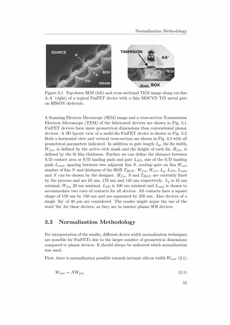
Normalization Methodology
BOXA
A’
FinDRAIN
SOURCE TiN/HfSiON36 nm
AA’
NiSi
Silicon
BOX
Figure 3.1: Top-down SEM (left) and cross sectional TEM image along cut-lineA-A’ (right) of a typical FinFET device with a thin MOCVD TiN metal gateon HfSiON dielectric.
A Scanning Electron Microscope (SEM) image and a cross-section TransmissionElectron Microscope (TEM) of the fabricated devices are shown in Fig. 3.1.FinFET devices have more geometrical dimensions than conventional planardevices. A 3D layout view of a multi-fin FinFET device is shown in Fig. 3.2.Both a horizontal view and vertical cross-section are shown in Fig. 3.3 with allgeometrical parameters indicated. In addition to gate length Lg, the fin width,Wfin, is defined by the active etch mask and the height of each fin, Hfin, isdefined by the Si film thickness. Further we can define the distance betweenS/D contact area or S/D landing pads and gate LSD, size of the S/D landingpads Lcont, spacing between two adjacent fins S, overlap gate on fins Wext,number of fins N and thickness of the BOX TBOX . Wfin, Wext, Lg, LSD, Lcont
and N can be chosen by the designer. Hfin, S and TBOX are currently fixedby the process and are 65 nm, 170 nm and 145 nm respectively. Lg is 45 nmminimal, Wfin 30 nm minimal, LSD is 100 nm minimal and Lcont is chosen toaccommodate two rows of contacts for all devices. All contacts have a squareshape of 150 nm by 150 nm and are separated by 250 nm. Also devices of asingle ’fin’ of 40 µm are considered. The reader might argue the use of theword ’fin’ for these devices, as they are in essence planar SOI devices.
3.3 Normalization Methodology
For interpretation of the results, different device width normalization techniquesare possible for FinFETs due to the larger number of geometrical dimensionscompared to planar devices. It should always be indicated which normalizationwas used.
First, there is normalization possible towards intrinsic silicon width Wintr (3.1).
Wintr = NWfin (3.1)
55
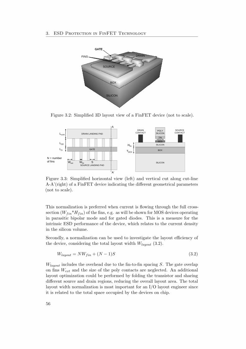
3. ESD Protection in FinFET Technology
GATE
DRAIN
SOURCE
FINS
BOX
SILICON
GATE
DRAIN
SOURCE
FINS
BOX
SILICON
Figure 3.2: Simplified 3D layout view of a FinFET device (not to scale).
GATE
SOURCE LANDING PAD
DRAIN LANDING PAD
LG
LSD
Lcont
Wext Wfin SN = numberof fins
A
A’
BOX
SILICON
POLYSILICON
TBOX
HfinSILICON
TiNHfSiON
SOURCECONTACT
DRAINCONTACT
SiO2
Figure 3.3: Simplified horizontal view (left) and vertical cut along cut-lineA-A’(right) of a FinFET device indicating the different geometrical parameters(not to scale).
This normalization is preferred when current is flowing through the full cross-section (Wfin*Hfin) of the fins, e.g. as will be shown for MOS devices operatingin parasitic bipolar mode and for gated diodes. This is a measure for theintrinsic ESD performance of the device, which relates to the current densityin the silicon volume.
Secondly, a normalization can be used to investigate the layout efficiency ofthe device, considering the total layout width Wlayout (3.2).
Wlayout = NWfin + (N − 1)S (3.2)
Wlayout includes the overhead due to the fin-to-fin spacing S. The gate overlapon fins Wext and the size of the poly contacts are neglected. An additionallayout optimization could be performed by folding the transistor and sharingdifferent source and drain regions, reducing the overall layout area. The totallayout width normalization is most important for an I/O layout engineer sinceit is related to the total space occupied by the devices on chip.
56
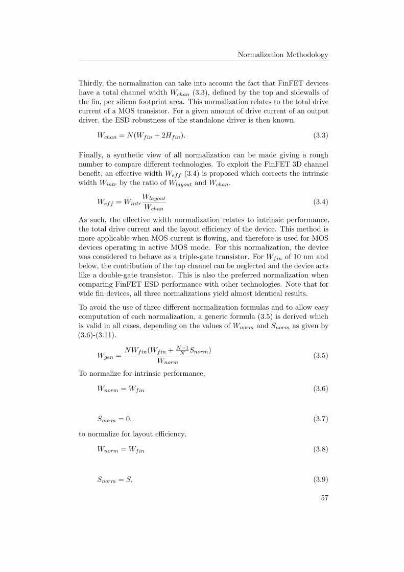
Normalization Methodology
Thirdly, the normalization can take into account the fact that FinFET deviceshave a total channel width Wchan (3.3), defined by the top and sidewalls ofthe fin, per silicon footprint area. This normalization relates to the total drivecurrent of a MOS transistor. For a given amount of drive current of an outputdriver, the ESD robustness of the standalone driver is then known.
Wchan = N(Wfin + 2Hfin). (3.3)
Finally, a synthetic view of all normalization can be made giving a roughnumber to compare different technologies. To exploit the FinFET 3D channelbenefit, an effective width Weff (3.4) is proposed which corrects the intrinsicwidth Wintr by the ratio of Wlayout and Wchan.
Weff = WintrWlayout
Wchan(3.4)
As such, the effective width normalization relates to intrinsic performance,the total drive current and the layout efficiency of the device. This method ismore applicable when MOS current is flowing, and therefore is used for MOSdevices operating in active MOS mode. For this normalization, the devicewas considered to behave as a triple-gate transistor. For Wfin of 10 nm andbelow, the contribution of the top channel can be neglected and the device actslike a double-gate transistor. This is also the preferred normalization whencomparing FinFET ESD performance with other technologies. Note that forwide fin devices, all three normalizations yield almost identical results.
To avoid the use of three different normalization formulas and to allow easycomputation of each normalization, a generic formula (3.5) is derived whichis valid in all cases, depending on the values of Wnorm and Snorm as given by(3.6)-(3.11).
Wgen =NWfin(Wfin + N−1
N Snorm)Wnorm
(3.5)
To normalize for intrinsic performance,
Wnorm = Wfin (3.6)
Snorm = 0, (3.7)
to normalize for layout efficiency,
Wnorm = Wfin (3.8)
Snorm = S, (3.9)
57
3. ESD Protection in FinFET Technology
to normalize for effective performance according to (3.4),
Wnorm = Wfin + 2Hfin (3.10)
Snorm = S. (3.11)
3.4 Geometrical Dependencies
The influence of the geometrical parameters, Lg, Wfin, N , Hfin, S and TBOX
in Fig. 3.3, on the different ESD performance parameters is investigated inthis section. Section 3.4.1 discusses the parasitic bipolar operation modewhere ESD stress is applied to the drain, while source and gate are grounded.Section 3.4.2 discusses the reverse polarity, where the device is operating inactive MOS mode. Gated diodes are discussed in section 3.4.3.
3.4.1 MOS devices - parasitic bipolar mode
ESD stress is applied to the drain, while source and gate are grounded. TheMOS devices are thus first in off-mode and later operated in parasitic bipolarmode, which means that each fin forms its own parasitic bipolar transistor. Theanalysis done in this section applies to both dedicated MOS ESD protectiondevices operating in bipolar mode and to MOS output drivers which could bemade self-protecting based on these results.
TLP measurements of narrow and wide fin NMOS and PMOS FinFET devicesare shown in Fig. 3.4 and Fig. 3.5 respectively for different gate lengths. Thelast point indicated in each IV-curve corresponds to the maximum failurecurrent It2. After the next TLP stress level, an increase in leakage currentwas noticed, indicating device failure. Extraction of It2, V t1, Vh and Ron isindicated in Fig. 3.4. The narrow fin devices have a Wfin of 30 nm and N is400, resulting in Wintr of 12 µm and Wlayout of 80 µm, according to section 3.3.The wide fin devices consist of a single ’fin’ of 40 µm wide resembling a planarSOI device. Since the parasitic bipolars have their bases floating, no snapbackis seen in the TLP I-V curves. This floating body effect is typical for anySOI process [Amer 02], even though for planar SOI a body contact could beprovided from the device side. The trigger voltage is not BVCBO as e.g. forbulk technologies, but the device starts to conduct current immediately at thelower BVCEO. This means that the trigger voltage, V t1, and holding voltage,Vh, are equal [Amer 02], which helps for uniform turn-on of all fingers. Both
58
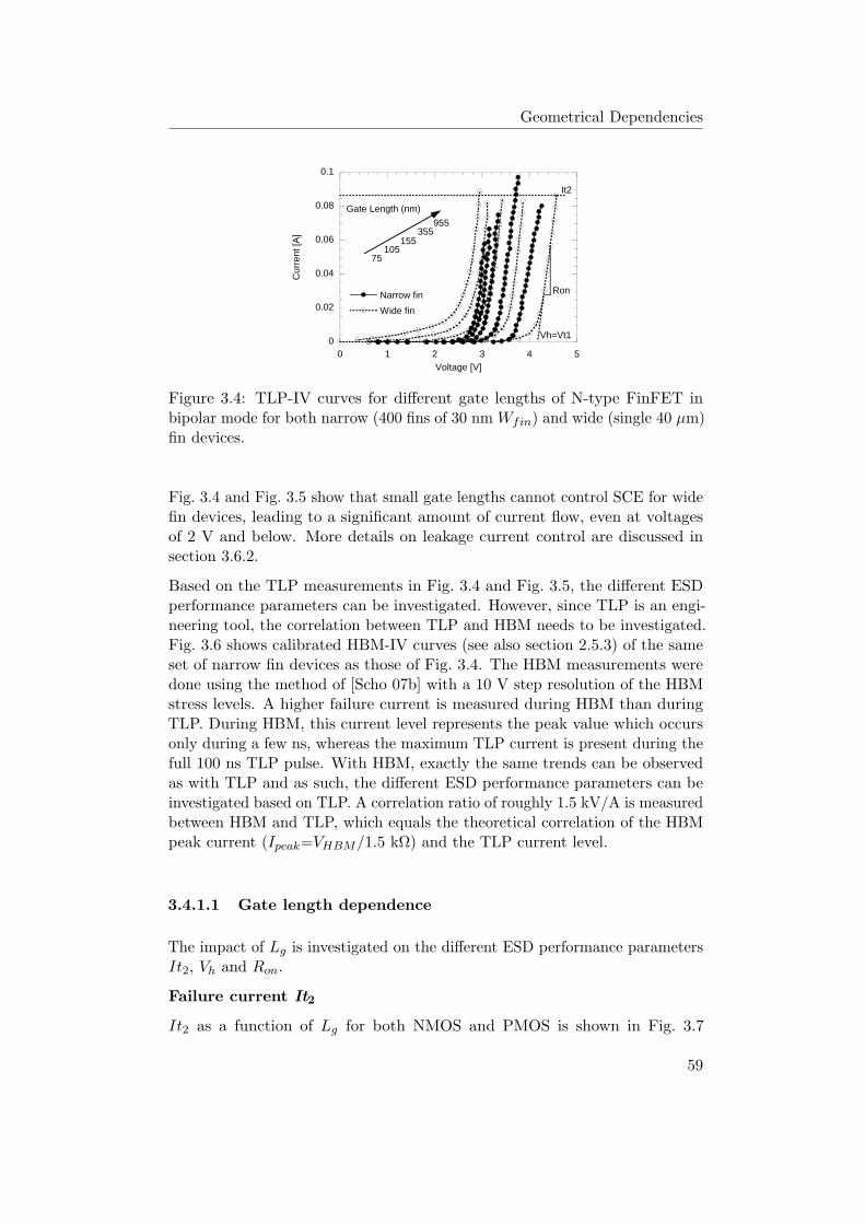
Geometrical Dependencies
0
0.02
0.04
0.06
0.08
0.1
0 1 2 3 4 5
Narrow fin
Wide fin
Cur
rent
[A]
Voltage [V]
75105
155355
955
Gate Length (nm)
It2
Vh=Vt1
Ron
Figure 3.4: TLP-IV curves for different gate lengths of N-type FinFET inbipolar mode for both narrow (400 fins of 30 nm Wfin) and wide (single 40 µm)fin devices.
Fig. 3.4 and Fig. 3.5 show that small gate lengths cannot control SCE for widefin devices, leading to a significant amount of current flow, even at voltagesof 2 V and below. More details on leakage current control are discussed insection 3.6.2.
Based on the TLP measurements in Fig. 3.4 and Fig. 3.5, the different ESDperformance parameters can be investigated. However, since TLP is an engi-neering tool, the correlation between TLP and HBM needs to be investigated.Fig. 3.6 shows calibrated HBM-IV curves (see also section 2.5.3) of the sameset of narrow fin devices as those of Fig. 3.4. The HBM measurements weredone using the method of [Scho 07b] with a 10 V step resolution of the HBMstress levels. A higher failure current is measured during HBM than duringTLP. During HBM, this current level represents the peak value which occursonly during a few ns, whereas the maximum TLP current is present during thefull 100 ns TLP pulse. With HBM, exactly the same trends can be observedas with TLP and as such, the different ESD performance parameters can beinvestigated based on TLP. A correlation ratio of roughly 1.5 kV/A is measuredbetween HBM and TLP, which equals the theoretical correlation of the HBMpeak current (Ipeak=VHBM/1.5 kΩ) and the TLP current level.
3.4.1.1 Gate length dependence
The impact of Lg is investigated on the different ESD performance parametersIt2, Vh and Ron.
Failure current It2
It2 as a function of Lg for both NMOS and PMOS is shown in Fig. 3.7
59
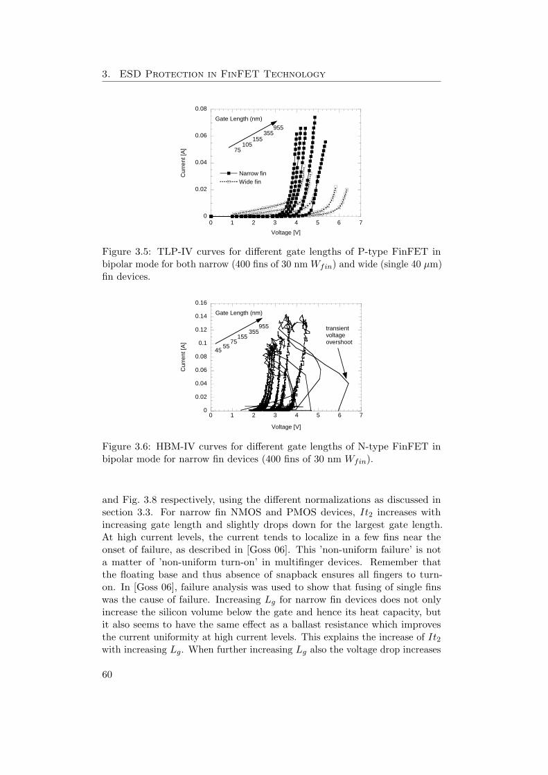
3. ESD Protection in FinFET Technology
0
0.02
0.04
0.06
0.08
0 1 2 3 4 5 6 7
Narrow finWide fin
Cur
rent
[A]
Voltage [V]
Gate Length (nm)
75105
155355
955
Figure 3.5: TLP-IV curves for different gate lengths of P-type FinFET inbipolar mode for both narrow (400 fins of 30 nm Wfin) and wide (single 40 µm)fin devices.
0
0.02
0.04
0.06
0.08
0.1
0.12
0.14
0.16
0 1 2 3 4 5 6 7
Cur
rent
[A]
Voltage [V]
Gate Length (nm)
75155
355955
5545
transientvoltageovershoot
Figure 3.6: HBM-IV curves for different gate lengths of N-type FinFET inbipolar mode for narrow fin devices (400 fins of 30 nm Wfin).
and Fig. 3.8 respectively, using the different normalizations as discussed insection 3.3. For narrow fin NMOS and PMOS devices, It2 increases withincreasing gate length and slightly drops down for the largest gate length.At high current levels, the current tends to localize in a few fins near theonset of failure, as described in [Goss 06]. This ’non-uniform failure’ is nota matter of ’non-uniform turn-on’ in multifinger devices. Remember thatthe floating base and thus absence of snapback ensures all fingers to turn-on. In [Goss 06], failure analysis was used to show that fusing of single finswas the cause of failure. Increasing Lg for narrow fin devices does not onlyincrease the silicon volume below the gate and hence its heat capacity, butit also seems to have the same effect as a ballast resistance which improvesthe current uniformity at high current levels. This explains the increase of It2with increasing Lg. When further increasing Lg also the voltage drop increases
60
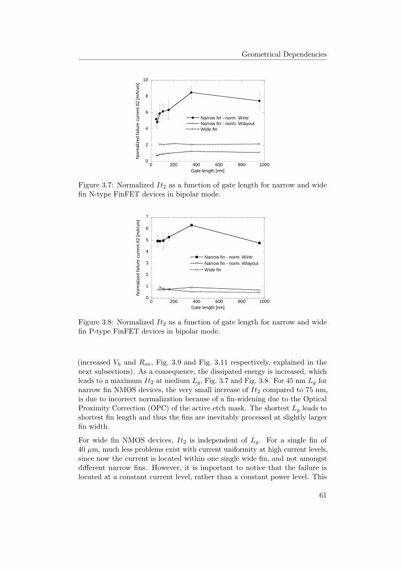
Geometrical Dependencies
0
2
4
6
8
10
0 200 400 600 800 1000
Narrow fin - norm. WintrNarrow fin - norm. WlayoutWide fin
Nor
mal
ized
failu
re c
urre
nt It
2 [m
A/u
m]
Gate length [nm]
Figure 3.7: Normalized It2 as a function of gate length for narrow and widefin N-type FinFET devices in bipolar mode.
0
1
2
3
4
5
6
7
0 200 400 600 800 1000
Narrow fin - norm. WintrNarrow fin - norm. WlayoutWide fin
Nor
mal
ized
failu
re c
urre
nt It
2 [m
A/u
m]
Gate length [nm]
Figure 3.8: Normalized It2 as a function of gate length for narrow and widefin P-type FinFET devices in bipolar mode.
(increased Vh and Ron, Fig. 3.9 and Fig. 3.11 respectively, explained in thenext subsections). As a consequence, the dissipated energy is increased, whichleads to a maximum It2 at medium Lg, Fig. 3.7 and Fig. 3.8. For 45 nm Lg fornarrow fin NMOS devices, the very small increase of It2 compared to 75 nm,is due to incorrect normalization because of a fin-widening due to the OpticalProximity Correction (OPC) of the active etch mask. The shortest Lg leads toshortest fin length and thus the fins are inevitably processed at slightly largerfin width.
For wide fin NMOS devices, It2 is independent of Lg. For a single fin of40 µm, much less problems exist with current uniformity at high current levels,since now the current is located within one single wide fin, and not amongstdifferent narrow fins. However, it is important to notice that the failure islocated at a constant current level, rather than a constant power level. This
61
3. ESD Protection in FinFET Technology
can be attributed to isothermal current instability which is initiated by impactionization under high field conditions [Vash 08]. Locally a high Joule powerlevel is generated which results in a filament formation and finally local burnout.This means that even within a single wide fin there can still exist a degree ofnon-uniformity.
In contrast to wide fin NMOS devices, Fig. 3.7, for PMOS devices It2 isdecreasing significantly for the largest Lg, Fig. 3.8. This can be attributed totheir high holding voltage (5-6 V) needed for bipolar action as seen in Fig. 3.5and Fig. 3.9. As such, these devices are failing because of gate-oxide breakdownat the drain-gate overlap region instead of thermal failure of the fins. Thisis described in more detail in section 3.4.1.3 where several parallel blocks ofdevices are considered. In case of thermal failure, scaling of the failure levelwith the number of parallel blocks should be obtained, which is not the casefor wide PMOS devices with large Lg.
A possible explanation for the current localization, described in [Goss 06], couldbe the existence of local Schottky contacts between the S/D silicide (NiSi) andthe body of the FinFETs [Hoff 05]. These results were obtained from similarIMEC silicon samples. Such a Schottky contact is a result of over-silicidationof the fins where the Ni-silicide can overrun the lowly doped extension regionand grow into the channel region. The ESD robustness is very sensitive toover-silicidation. However, in a more mature technology, the problem of over-silicidation should be greatly reduced. Many arguments point to the negativeimpact of the over-silicidation. First, the over-silicidation is worst for narrowfin devices [Coll 07], where much more statistical variation is measured thanfor wide fin devices. Secondly, over-silicidation is less problematic for PMOSdevices as Boron retards the silicidation [Coll 07] [Dixi 06]. This can explainthe increased It2 for PMOS devices with smallest gate length when comparedto NMOS and the reduced Lg dependency, Fig. 3.7 and Fig. 3.8. Also, muchless statistical variation in It2 was measured on PMOS than on NMOS devices.The error bars indicating the standard deviation of It2 for NMOS and PMOSdevices in Fig. 3.7 and Fig. 3.8 for Wintr normalization show the increasedvariability for NMOS. Finally, over-silicidation is reduced by processing optionslike silicide blocking and SEG, which directly translates into an increased ESDperformance as described further in section 3.6.
For wide fin NMOS devices, It2 is equal to 2 mA/µm and independent of Lg,Fig. 3.7. The ESD robustness for narrow fin NMOS devices is 0.5 to 1 mA/µmwhen normalized to Wlayout. However, the robustness regarding Wintr is 5 to8 mA/µm, representing an even higher intrinsic It2 than the results reportedfor planar SOI devices [Kepp 06]. This is explained by looking at the fin widthdependence of It2 in section 3.4.1.2.
62
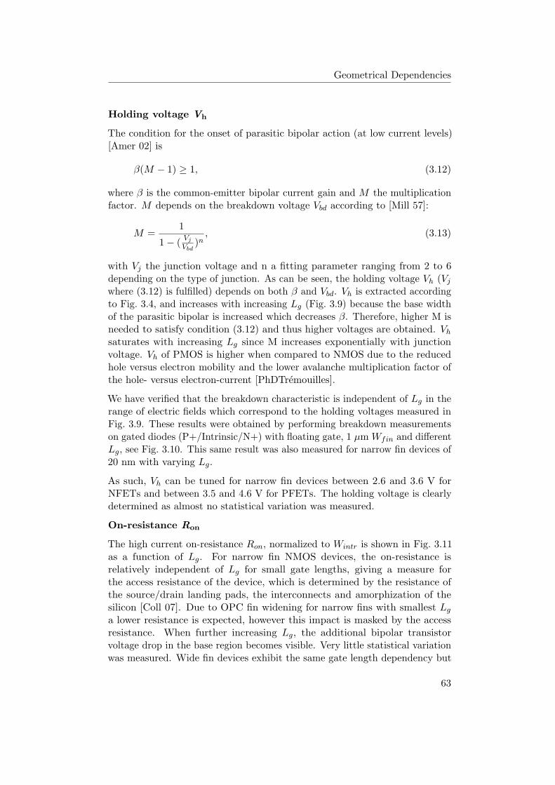
Geometrical Dependencies
Holding voltage Vh
The condition for the onset of parasitic bipolar action (at low current levels)[Amer 02] is
β(M − 1) ≥ 1, (3.12)
where β is the common-emitter bipolar current gain and M the multiplicationfactor. M depends on the breakdown voltage Vbd according to [Mill 57]:
M =1
1− ( Vj
Vbd)n
, (3.13)
with Vj the junction voltage and n a fitting parameter ranging from 2 to 6depending on the type of junction. As can be seen, the holding voltage Vh (Vj
where (3.12) is fulfilled) depends on both β and Vbd. Vh is extracted accordingto Fig. 3.4, and increases with increasing Lg (Fig. 3.9) because the base widthof the parasitic bipolar is increased which decreases β. Therefore, higher M isneeded to satisfy condition (3.12) and thus higher voltages are obtained. Vh
saturates with increasing Lg since M increases exponentially with junctionvoltage. Vh of PMOS is higher when compared to NMOS due to the reducedhole versus electron mobility and the lower avalanche multiplication factor ofthe hole- versus electron-current [PhDTremouilles].
We have verified that the breakdown characteristic is independent of Lg in therange of electric fields which correspond to the holding voltages measured inFig. 3.9. These results were obtained by performing breakdown measurementson gated diodes (P+/Intrinsic/N+) with floating gate, 1 µm Wfin and differentLg, see Fig. 3.10. This same result was also measured for narrow fin devices of20 nm with varying Lg.
As such, Vh can be tuned for narrow fin devices between 2.6 and 3.6 V forNFETs and between 3.5 and 4.6 V for PFETs. The holding voltage is clearlydetermined as almost no statistical variation was measured.
On-resistance Ron
The high current on-resistance Ron, normalized to Wintr is shown in Fig. 3.11as a function of Lg. For narrow fin NMOS devices, the on-resistance isrelatively independent of Lg for small gate lengths, giving a measure forthe access resistance of the device, which is determined by the resistance ofthe source/drain landing pads, the interconnects and amorphization of thesilicon [Coll 07]. Due to OPC fin widening for narrow fins with smallest Lg
a lower resistance is expected, however this impact is masked by the accessresistance. When further increasing Lg, the additional bipolar transistorvoltage drop in the base region becomes visible. Very little statistical variationwas measured. Wide fin devices exhibit the same gate length dependency but
63
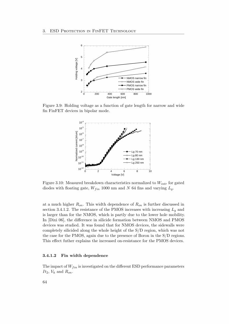
3. ESD Protection in FinFET Technology
2
3
4
5
6
0 200 400 600 800 1000
NMOS narrow finNMOS wide finPMOS narrow finPMOS wide fin
Hol
ding
vol
tage
[V]
Gate length [nm]
Figure 3.9: Holding voltage as a function of gate length for narrow and widefin FinFET devices in bipolar mode.
10-12
10-11
10-10
10-9
10-8
10-7
10-6
10-5
10-4
0 2 4 6 8 10
Lg 70 nmLg 80 nmLg 130 nmLg 250 nm
Nor
mal
ized
cur
rent
[A/u
m]
Voltage [V]
Figure 3.10: Measured breakdown characteristics normalized to Wintr for gateddiodes with floating gate, Wfin 1000 nm and N 64 fins and varying Lg.
at a much higher Ron. This width dependence of Ron is further discussed insection 3.4.1.2. The resistance of the PMOS increases with increasing Lg andis larger than for the NMOS, which is partly due to the lower hole mobility.In [Dixi 06], the difference in silicide formation between NMOS and PMOSdevices was studied. It was found that for NMOS devices, the sidewalls werecompletely silicided along the whole height of the S/D region, which was notthe case for the PMOS, again due to the presence of Boron in the S/D regions.This effect futher explains the increased on-resistance for the PMOS devices.
3.4.1.2 Fin width dependence
The impact of Wfin is investigated on the different ESD performance parametersIt2, Vh and Ron.
64
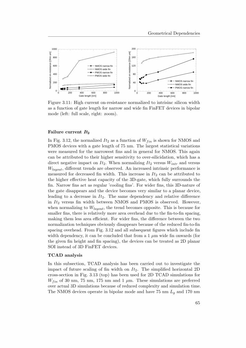
Geometrical Dependencies
0
200
400
600
800
1000
0 200 400 600 800 1000
NMOS narrow finNMOS wide finPMOS narrow finPMOS wide fin
Nor
mal
ized
on-
resi
stan
ce [O
hm u
m]
Gate length [nm]
0
40
80
120
160
200
0 200 400 600 800 1000
NMOS narrow finNMOS wide finPMOS narrow finN
orm
aliz
ed o
n-re
sist
ance
[Ohm
um
]
Gate length [nm]
Figure 3.11: High current on-resistance normalized to intrisinc silicon widthas a function of gate length for narrow and wide fin FinFET devices in bipolarmode (left: full scale, right: zoom).
Failure current It2
In Fig. 3.12, the normalized It2 as a function of Wfin is shown for NMOS andPMOS devices with a gate length of 75 nm. The largest statistical variationswere measured for the narrowest fins and in general for NMOS. This againcan be attributed to their higher sensitivity to over-silicidation, which has adirect negative impact on It2. When normalizing It2 versus Wintr and versusWlayout, different trends are observed. An increased intrinsic performance ismeasured for decreased fin width. This increase in It2 can be attributed tothe higher effective heat capacity of the 3D-gate, which fully surrounds thefin. Narrow fins act as regular ’cooling fins’. For wider fins, this 3D-nature ofthe gate disappears and the device becomes very similar to a planar device,leading to a decrease in It2. The same dependency and relative differencein It2 versus fin width between NMOS and PMOS is observed. However,when normalizing to Wlayout, the trend becomes opposite. This is because forsmaller fins, there is relatively more area overhead due to the fin-to-fin spacing,making them less area efficient. For wider fins, the difference between the twonormalization techniques obviously disappears because of the reduced fin-to-finspacing overhead. From Fig. 3.12 and all subsequent figures which include finwidth dependency, it can be concluded that from a 1 µm wide fin onwards (forthe given fin height and fin spacing), the devices can be treated as 2D planarSOI instead of 3D FinFET devices.
TCAD analysis
In this subsection, TCAD analysis has been carried out to investigate theimpact of future scaling of fin width on It2. The simplified horizontal 2Dcross-section in Fig. 3.13 (top) has been used for 2D TCAD simulations forWfin of 30 nm, 75 nm, 175 nm and 1 µm. These simulations are preferredover actual 3D simulations because of reduced complexity and simulation time.The NMOS devices operate in bipolar mode and have 75 nm Lg and 170 nm
65
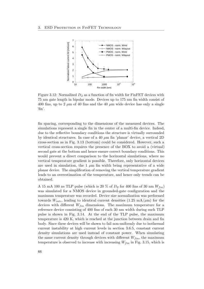
3. ESD Protection in FinFET Technology
0
1
2
3
4
5
6
7
10 100 1000 104 105
NMOS - norm. WintrNMOS - norm. WlayoutPMOS - norm. WintrPMOS - norm. Wlayout
Nor
mal
ized
failu
re c
urre
nt It
2 [m
A/u
m]
Fin width [nm]
Figure 3.12: Normalized It2 as a function of fin width for FinFET devices with75 nm gate length in bipolar mode. Devices up to 175 nm fin width consist of400 fins, up to 2 µm of 40 fins and the 40 µm wide device has only a single’fin’.
fin spacing, corresponding to the dimensions of the measured devices. Thesimulations represent a single fin in the center of a multi-fin device. Indeed,due to the reflective boundary conditions the structure is virtually surroundedby identical structures. In case of a 40 µm fin ’planar’ device, a vertical 2Dcross-section as in Fig. 3.13 (bottom) could be considered. However, such avertical cross-section requires the presence of the BOX to avoid a (virtual)second gate at the bottom and hence ensure correct boundary conditions. Thiswould prevent a direct comparison to the horizontal simulations, where novertical temperature gradient is possible. Therefore, only horizontal devicesare used in simulation, the 1 µm fin width being representative of a wideplanar device. The simplification of removing the vertical temperature gradientleads to an overestimation of the temperature, and hence only trends can beobtained.
A 15 mA 100 ns TLP pulse (which is 20 % of It2 for 400 fins of 30 nm Wfin)was simulated for a NMOS device in grounded-gate configuration and themaximum temperature was recorded. Device size normalization was performedtowards Wintr, leading to identical current densities (1.25 mA/µm) for thedevices with different Wfin dimensions. The maximum temperature for areference device consisting of 400 fins of each 30 nm width during such TLPpulse is shown in Fig. 3.14. At the end of the TLP pulse, the maximumtemperature is 420 K, which is reached at the junction between drain and finbody. Since these devices will be shown to fail non-uniformly due to isothermalcurrent instability at high current levels in section 3.6.5, constant currentdensity simulations are used instead of constant power. When simulatingthe same current density through devices with different Wfin, the maximumtemperature is observed to increase with increasing Wfin in Fig. 3.15, which is
66
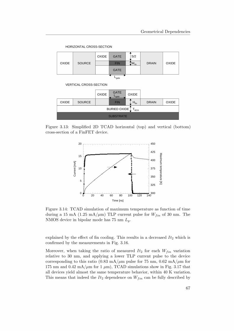
Geometrical Dependencies
FINSOURCE DRAINOXIDE OXIDE
OXIDE GATE
Lgate
S/2
Wfin
SOURCE DRAIN
OXIDEGATE
FIN
Lgate
Hfin
OXIDE
FIN OXIDEOXIDE
HORIZONTAL CROSS-SECTION
VERTICAL CROSS-SECTION
GATE
BURIED OXIDE
SUBSTRATE
TBOX
Figure 3.13: Simplified 2D TCAD horizontal (top) and vertical (bottom)cross-section of a FinFET device.
0
5
10
15
20
300
325
350
375
400
425
450
0 20 40 60 80 100 120 140
Cur
rent
[mA
]M
aximum
temperature [K
]
Time [ns]
Figure 3.14: TCAD simulation of maximum temperature as function of timeduring a 15 mA (1.25 mA/µm) TLP current pulse for Wfin of 30 nm. TheNMOS device in bipolar mode has 75 nm Lg.
explained by the effect of fin cooling. This results in a decreased It2 which isconfirmed by the measurements in Fig. 3.16.
Moreover, when taking the ratio of measured It2 for each Wfin variationrelative to 30 nm, and applying a lower TLP current pulse to the devicecorresponding to this ratio (0.83 mA/µm pulse for 75 nm, 0.62 mA/µm for175 nm and 0.42 mA/µm for 1 µm), TCAD simulations show in Fig. 3.17 thatall devices yield almost the same temperature behavior, within 40 K variation.This means that indeed the It2 dependence on Wfin can be fully described by
67
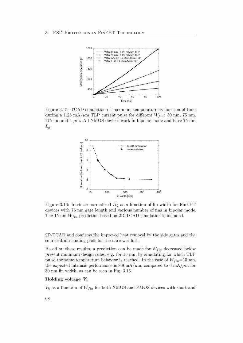
3. ESD Protection in FinFET Technology
400
600
800
1000
1200
0 20 40 60 80 100
Wfin 30 nm - 1.25 mA/um TLPWfin 75 nm - 1.25 mA/um TLPWfin 175 nm - 1.25 mA/um TLPWfin 1 µm - 1.25 mA/um TLP
Max
imum
tem
pera
ture
[K]
Time [ns]
Figure 3.15: TCAD simulation of maximum temperature as function of timeduring a 1.25 mA/µm TLP current pulse for different Wfin: 30 nm, 75 nm,175 nm and 1 µm. All NMOS devices work in bipolar mode and have 75 nmLg.
0
2
4
6
8
10
10 100 1000 104 105
TCAD simulationmeasurement
Nor
mal
ized
failu
re c
urre
nt It
2 [m
A/u
m]
Fin width [nm]
Figure 3.16: Intrinsic normalized It2 as a function of fin width for FinFETdevices with 75 nm gate length and various number of fins in bipolar mode.The 15 nm Wfin prediction based on 2D-TCAD simulation is included.
2D-TCAD and confirms the improved heat removal by the side gates and thesource/drain landing pads for the narrower fins.
Based on these results, a prediction can be made for Wfin decreased belowpresent minimum design rules, e.g. for 15 nm, by simulating for which TLPpulse the same temperature behavior is reached. In the case of Wfin=15 nm,the expected intrinsic performance is 8.9 mA/µm, compared to 6 mA/µm for30 nm fin width, as can be seen in Fig. 3.16.
Holding voltage Vh
Vh as a function of Wfin for both NMOS and PMOS devices with short and
68
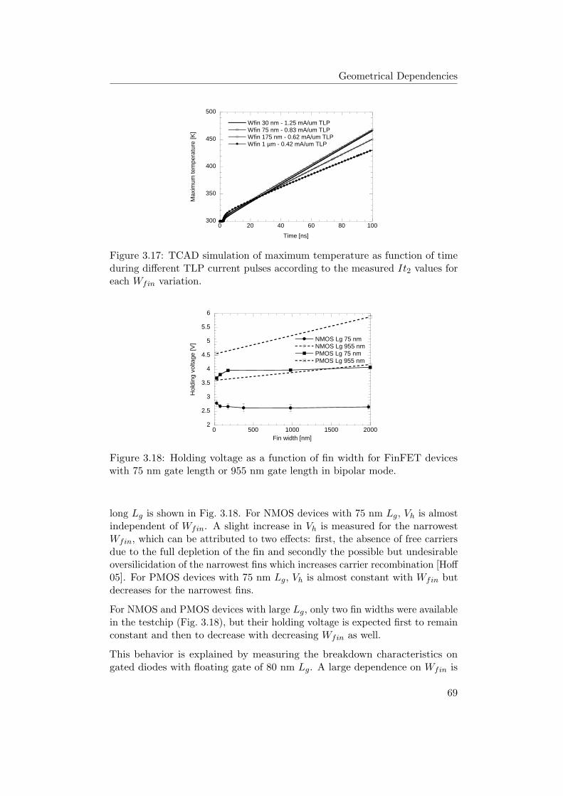
Geometrical Dependencies
300
350
400
450
500
0 20 40 60 80 100
Wfin 30 nm - 1.25 mA/um TLPWfin 75 nm - 0.83 mA/um TLPWfin 175 nm - 0.62 mA/um TLPWfin 1 µm - 0.42 mA/um TLP
Max
imum
tem
pera
ture
[K]
Time [ns]
Figure 3.17: TCAD simulation of maximum temperature as function of timeduring different TLP current pulses according to the measured It2 values foreach Wfin variation.
2
2.5
3
3.5
4
4.5
5
5.5
6
0 500 1000 1500 2000
NMOS Lg 75 nmNMOS Lg 955 nmPMOS Lg 75 nmPMOS Lg 955 nm
Hol
ding
vol
tage
[V]
Fin width [nm]
Figure 3.18: Holding voltage as a function of fin width for FinFET deviceswith 75 nm gate length or 955 nm gate length in bipolar mode.
long Lg is shown in Fig. 3.18. For NMOS devices with 75 nm Lg, Vh is almostindependent of Wfin. A slight increase in Vh is measured for the narrowestWfin, which can be attributed to two effects: first, the absence of free carriersdue to the full depletion of the fin and secondly the possible but undesirableoversilicidation of the narrowest fins which increases carrier recombination [Hoff05]. For PMOS devices with 75 nm Lg, Vh is almost constant with Wfin butdecreases for the narrowest fins.
For NMOS and PMOS devices with large Lg, only two fin widths were availablein the testchip (Fig. 3.18), but their holding voltage is expected first to remainconstant and then to decrease with decreasing Wfin as well.
This behavior is explained by measuring the breakdown characteristics ongated diodes with floating gate of 80 nm Lg. A large dependence on Wfin is
69
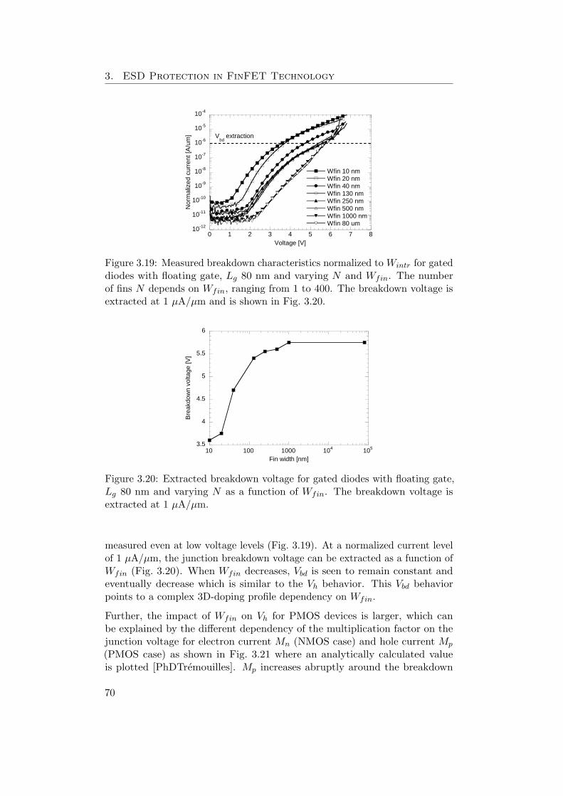
3. ESD Protection in FinFET Technology
10-12
10-11
10-10
10-9
10-8
10-7
10-6
10-5
10-4
0 1 2 3 4 5 6 7 8
Wfin 10 nmWfin 20 nmWfin 40 nmWfin 130 nmWfin 250 nmWfin 500 nmWfin 1000 nmWfin 80 um
Nor
mal
ized
cur
rent
[A/u
m]
Voltage [V]
Vbd
extraction
Figure 3.19: Measured breakdown characteristics normalized to Wintr for gateddiodes with floating gate, Lg 80 nm and varying N and Wfin. The numberof fins N depends on Wfin, ranging from 1 to 400. The breakdown voltage isextracted at 1 µA/µm and is shown in Fig. 3.20.
3.5
4
4.5
5
5.5
6
10 100 1000 104 105
Bre
akdo
wn
volta
ge [V
]
Fin width [nm]
Figure 3.20: Extracted breakdown voltage for gated diodes with floating gate,Lg 80 nm and varying N as a function of Wfin. The breakdown voltage isextracted at 1 µA/µm.
measured even at low voltage levels (Fig. 3.19). At a normalized current levelof 1 µA/µm, the junction breakdown voltage can be extracted as a function ofWfin (Fig. 3.20). When Wfin decreases, Vbd is seen to remain constant andeventually decrease which is similar to the Vh behavior. This Vbd behaviorpoints to a complex 3D-doping profile dependency on Wfin.
Further, the impact of Wfin on Vh for PMOS devices is larger, which canbe explained by the different dependency of the multiplication factor on thejunction voltage for electron current Mn (NMOS case) and hole current Mp
(PMOS case) as shown in Fig. 3.21 where an analytically calculated valueis plotted [PhDTremouilles]. Mp increases abruptly around the breakdown
70
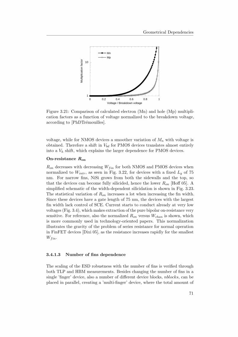
Geometrical Dependencies
1
10
0 0.2 0.4 0.6 0.8 1
Mn
Mp
Mul
tiplic
atio
n fa
ctor
Voltage / Breakdown voltage
Figure 3.21: Comparison of calculated electron (Mn) and hole (Mp) multipli-cation factors as a function of voltage normalized to the breakdown voltage,according to [PhDTremouilles].
voltage, while for NMOS devices a smoother variation of Mn with voltage isobtained. Therefore a shift in Vbd for PMOS devices translates almost entirelyinto a Vh shift, which explains the larger dependence for PMOS devices.
On-resistance Ron
Ron decreases with decreasing Wfin for both NMOS and PMOS devices whennormalized to Wintr, as seen in Fig. 3.22, for devices with a fixed Lg of 75nm. For narrow fins, NiSi grows from both the sidewalls and the top, sothat the devices can become fully silicided, hence the lower Ron [Hoff 05]. Asimplified schematic of the width-dependent silicidation is shown in Fig. 3.23.The statistical variation of Ron increases a lot when increasing the fin width.Since these devices have a gate length of 75 nm, the devices with the largestfin width lack control of SCE. Current starts to conduct already at very lowvoltages (Fig. 3.4), which makes extraction of the pure bipolar on-resistance verysensitive. For reference, also the normalized Ron versus Wchan is shown, whichis more commonly used in technology-oriented papers. This normalizationillustrates the gravity of the problem of series resistance for normal operationin FinFET devices [Dixi 05], as the resistance increases rapidly for the smallestWfin.
3.4.1.3 Number of fins dependence
The scaling of the ESD robustness with the number of fins is verified throughboth TLP and HBM measurements. Besides changing the number of fins in asingle ’finger’ device, also a number of different device blocks, nblocks, can beplaced in parallel, creating a ’multi-finger’ device, where the total amount of
71
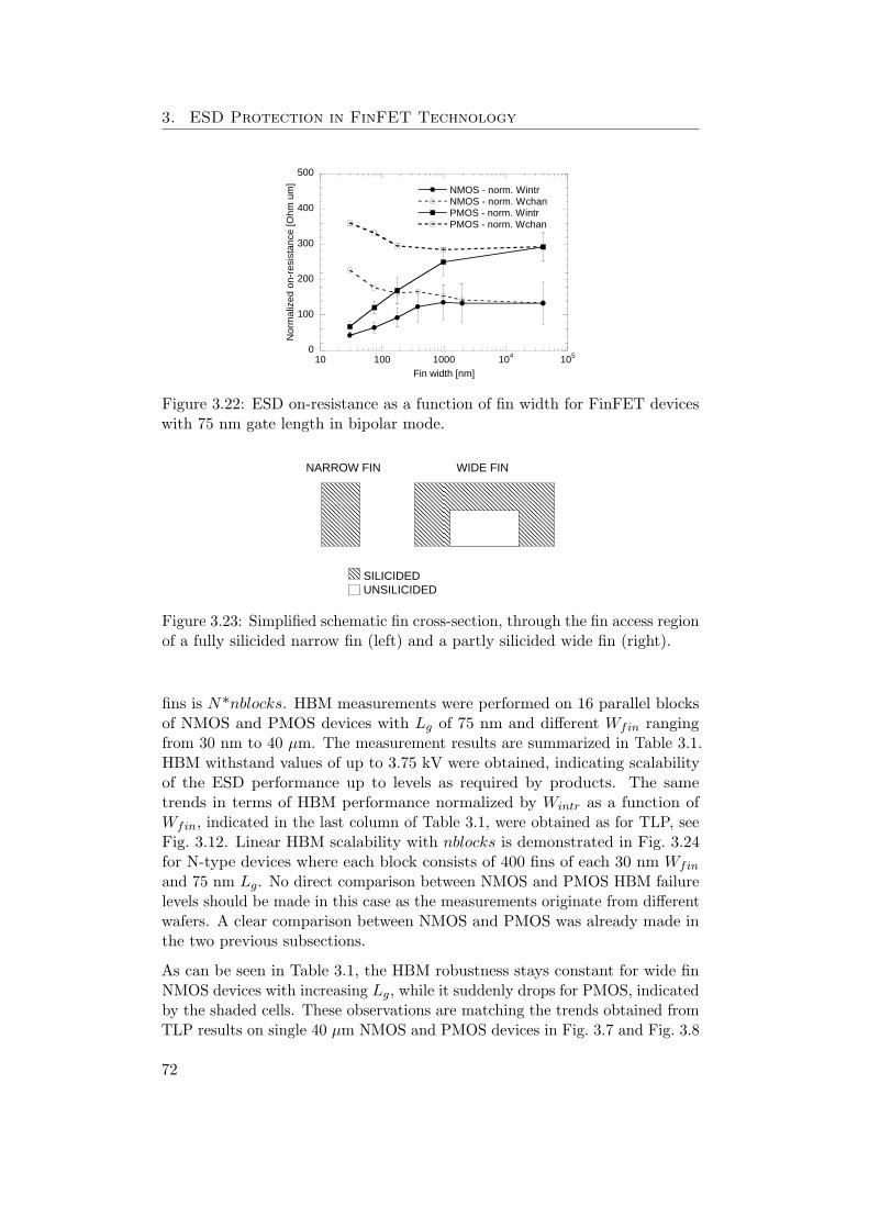
3. ESD Protection in FinFET Technology
0
100
200
300
400
500
10 100 1000 104 105
NMOS - norm. WintrNMOS - norm. WchanPMOS - norm. WintrPMOS - norm. Wchan
Nor
mal
ized
on-
resi
stan
ce [O
hm u
m]
Fin width [nm]
Figure 3.22: ESD on-resistance as a function of fin width for FinFET deviceswith 75 nm gate length in bipolar mode.
SILICIDEDUNSILICIDED
NARROW FIN WIDE FIN
Figure 3.23: Simplified schematic fin cross-section, through the fin access regionof a fully silicided narrow fin (left) and a partly silicided wide fin (right).
fins is N*nblocks. HBM measurements were performed on 16 parallel blocksof NMOS and PMOS devices with Lg of 75 nm and different Wfin rangingfrom 30 nm to 40 µm. The measurement results are summarized in Table 3.1.HBM withstand values of up to 3.75 kV were obtained, indicating scalabilityof the ESD performance up to levels as required by products. The sametrends in terms of HBM performance normalized by Wintr as a function ofWfin, indicated in the last column of Table 3.1, were obtained as for TLP, seeFig. 3.12. Linear HBM scalability with nblocks is demonstrated in Fig. 3.24for N-type devices where each block consists of 400 fins of each 30 nm Wfin
and 75 nm Lg. No direct comparison between NMOS and PMOS HBM failurelevels should be made in this case as the measurements originate from differentwafers. A clear comparison between NMOS and PMOS was already made inthe two previous subsections.
As can be seen in Table 3.1, the HBM robustness stays constant for wide finNMOS devices with increasing Lg, while it suddenly drops for PMOS, indicatedby the shaded cells. These observations are matching the trends obtained fromTLP results on single 40 µm NMOS and PMOS devices in Fig. 3.7 and Fig. 3.8
72
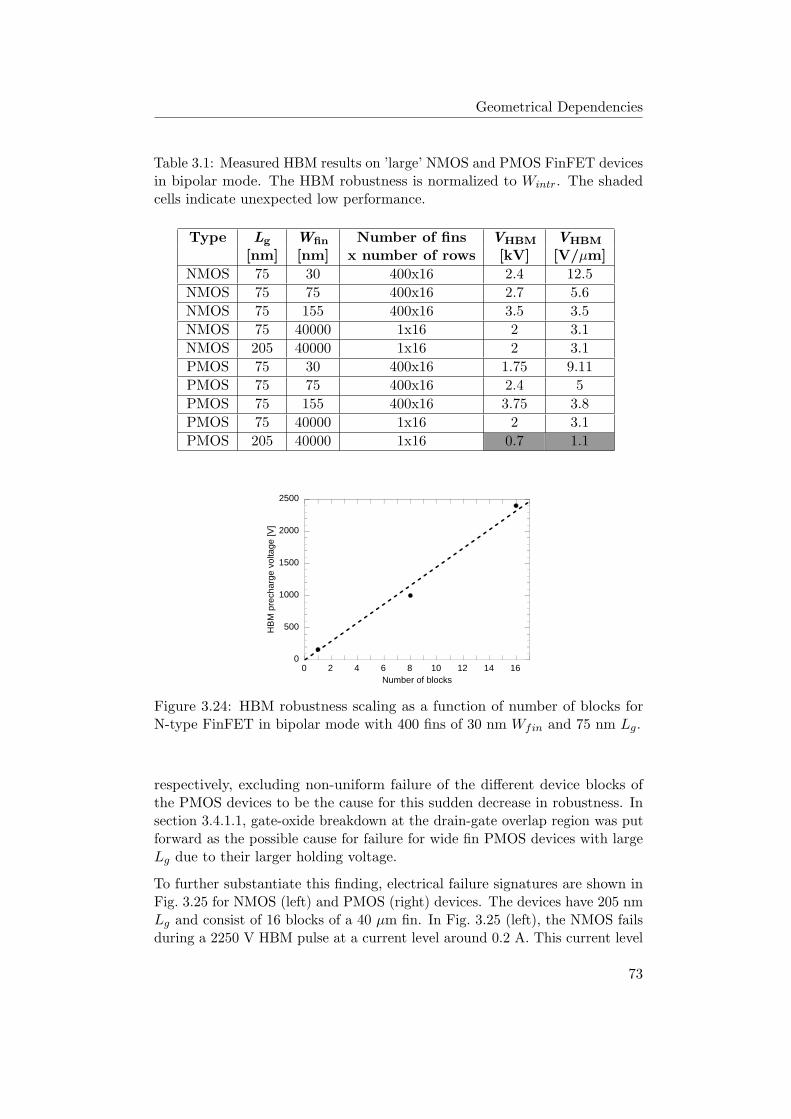
Geometrical Dependencies
Table 3.1: Measured HBM results on ’large’ NMOS and PMOS FinFET devicesin bipolar mode. The HBM robustness is normalized to Wintr. The shadedcells indicate unexpected low performance.
Type Lg Wfin Number of fins VHBM VHBM
[nm] [nm] x number of rows [kV] [V/µm]NMOS 75 30 400x16 2.4 12.5NMOS 75 75 400x16 2.7 5.6NMOS 75 155 400x16 3.5 3.5NMOS 75 40000 1x16 2 3.1NMOS 205 40000 1x16 2 3.1PMOS 75 30 400x16 1.75 9.11PMOS 75 75 400x16 2.4 5PMOS 75 155 400x16 3.75 3.8PMOS 75 40000 1x16 2 3.1PMOS 205 40000 1x16 0.7 1.1
0
500
1000
1500
2000
2500
0 2 4 6 8 10 12 14 16
HB
M p
rech
arge
vol
tage
[V]
Number of blocks
Figure 3.24: HBM robustness scaling as a function of number of blocks forN-type FinFET in bipolar mode with 400 fins of 30 nm Wfin and 75 nm Lg.
respectively, excluding non-uniform failure of the different device blocks ofthe PMOS devices to be the cause for this sudden decrease in robustness. Insection 3.4.1.1, gate-oxide breakdown at the drain-gate overlap region was putforward as the possible cause for failure for wide fin PMOS devices with largeLg due to their larger holding voltage.
To further substantiate this finding, electrical failure signatures are shown inFig. 3.25 for NMOS (left) and PMOS (right) devices. The devices have 205 nmLg and consist of 16 blocks of a 40 µm fin. In Fig. 3.25 (left), the NMOS failsduring a 2250 V HBM pulse at a current level around 0.2 A. This current level
73
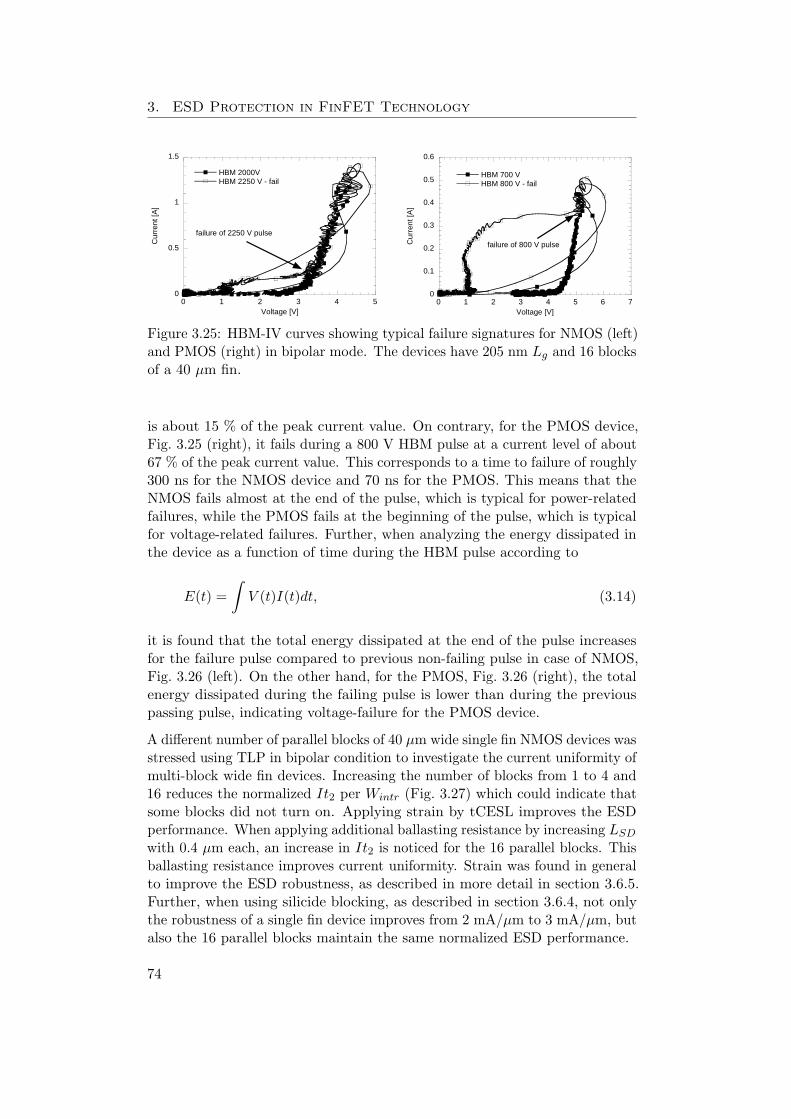
3. ESD Protection in FinFET Technology
0
0.5
1
1.5
0 1 2 3 4 5
HBM 2000VHBM 2250 V - fail
Cur
rent
[A]
Voltage [V]
failure of 2250 V pulse
0
0.1
0.2
0.3
0.4
0.5
0.6
0 1 2 3 4 5 6 7
HBM 700 VHBM 800 V - fail
Cur
rent
[A]
Voltage [V]
failure of 800 V pulse
Figure 3.25: HBM-IV curves showing typical failure signatures for NMOS (left)and PMOS (right) in bipolar mode. The devices have 205 nm Lg and 16 blocksof a 40 µm fin.
is about 15 % of the peak current value. On contrary, for the PMOS device,Fig. 3.25 (right), it fails during a 800 V HBM pulse at a current level of about67 % of the peak current value. This corresponds to a time to failure of roughly300 ns for the NMOS device and 70 ns for the PMOS. This means that theNMOS fails almost at the end of the pulse, which is typical for power-relatedfailures, while the PMOS fails at the beginning of the pulse, which is typicalfor voltage-related failures. Further, when analyzing the energy dissipated inthe device as a function of time during the HBM pulse according to
E(t) =∫
V (t)I(t)dt, (3.14)
it is found that the total energy dissipated at the end of the pulse increasesfor the failure pulse compared to previous non-failing pulse in case of NMOS,Fig. 3.26 (left). On the other hand, for the PMOS, Fig. 3.26 (right), the totalenergy dissipated during the failing pulse is lower than during the previouspassing pulse, indicating voltage-failure for the PMOS device.
A different number of parallel blocks of 40 µm wide single fin NMOS devices wasstressed using TLP in bipolar condition to investigate the current uniformity ofmulti-block wide fin devices. Increasing the number of blocks from 1 to 4 and16 reduces the normalized It2 per Wintr (Fig. 3.27) which could indicate thatsome blocks did not turn on. Applying strain by tCESL improves the ESDperformance. When applying additional ballasting resistance by increasing LSD
with 0.4 µm each, an increase in It2 is noticed for the 16 parallel blocks. Thisballasting resistance improves current uniformity. Strain was found in generalto improve the ESD robustness, as described in more detail in section 3.6.5.Further, when using silicide blocking, as described in section 3.6.4, not onlythe robustness of a single fin device improves from 2 mA/µm to 3 mA/µm, butalso the 16 parallel blocks maintain the same normalized ESD performance.
74
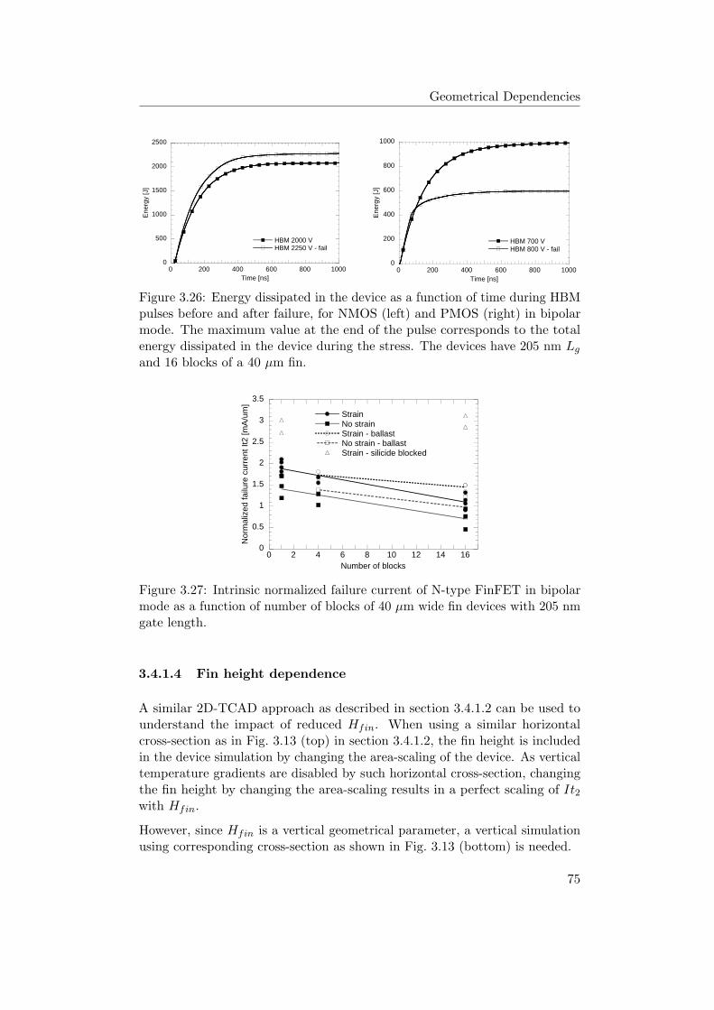
Geometrical Dependencies
0
500
1000
1500
2000
2500
0 200 400 600 800 1000
HBM 2000 VHBM 2250 V - fail
Ene
rgy
[J]
Time [ns]
0
200
400
600
800
1000
0 200 400 600 800 1000
HBM 700 VHBM 800 V - fail
Ene
rgy
[J]
Time [ns]
Figure 3.26: Energy dissipated in the device as a function of time during HBMpulses before and after failure, for NMOS (left) and PMOS (right) in bipolarmode. The maximum value at the end of the pulse corresponds to the totalenergy dissipated in the device during the stress. The devices have 205 nm Lg
and 16 blocks of a 40 µm fin.
0
0.5
1
1.5
2
2.5
3
3.5
0 2 4 6 8 10 12 14 16
StrainNo strainStrain - ballastNo strain - ballastStrain - silicide blocked
Nor
mal
ized
failu
re c
urre
nt It
2 [m
A/u
m]
Number of blocks
Figure 3.27: Intrinsic normalized failure current of N-type FinFET in bipolarmode as a function of number of blocks of 40 µm wide fin devices with 205 nmgate length.
3.4.1.4 Fin height dependence
A similar 2D-TCAD approach as described in section 3.4.1.2 can be used tounderstand the impact of reduced Hfin. When using a similar horizontalcross-section as in Fig. 3.13 (top) in section 3.4.1.2, the fin height is includedin the device simulation by changing the area-scaling of the device. As verticaltemperature gradients are disabled by such horizontal cross-section, changingthe fin height by changing the area-scaling results in a perfect scaling of It2with Hfin.
However, since Hfin is a vertical geometrical parameter, a vertical simulationusing corresponding cross-section as shown in Fig. 3.13 (bottom) is needed.
75
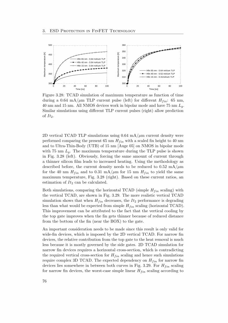
3. ESD Protection in FinFET Technology
300
350
400
450
500
0 20 40 60 80 100
Hfin 65 nm - 0.64 mA/um TLP
Hfin 40 nm - 0.64 mA/um TLP
Hfin 15 nm - 0.64 mA/um TLP
Max
imum
tem
pera
ture
[K]
Time [ns]
300
310
320
330
340
350
360
0 20 40 60 80 100
Hfin 65 nm - 0.64 mA/um TLP
Hfin 40 nm - 0.52 mA/um TLP
Hfin 15 nm - 0.31mA/um TLPMax
imum
tem
pera
ture
[K]
Time [ns]
Figure 3.28: TCAD simulation of maximum temperature as function of timeduring a 0.64 mA/µm TLP current pulse (left) for different Hfin: 65 nm,40 nm and 15 nm. All NMOS devices work in bipolar mode and have 75 nm Lg.Similar simulations using different TLP current pulses (right) allow predictionof It2.
2D vertical TCAD TLP simulations using 0.64 mA/µm current density wereperformed comparing the present 65 nm Hfin with a scaled fin height to 40 nmand to Ultra-Thin-Body (UTB) of 15 nm [Auge 05] on NMOS in bipolar modewith 75 nm Lg. The maximum temperature during the TLP pulse is shownin Fig. 3.28 (left). Obviously, forcing the same amount of current througha thinner silicon film leads to increased heating. Using the methodology asdescribed before, the current density needs to be reduced to 0.52 mA/µmfor the 40 nm Hfin and to 0.31 mA/µm for 15 nm Hfin to yield the samemaximum temperature, Fig. 3.28 (right). Based on these current ratios, anestimation of It2 can be calculated.
Both simulations, comparing the horizontal TCAD (simple Hfin scaling) withthe vertical TCAD, are shown in Fig. 3.29. The more realistic vertical TCADsimulation shows that when Hfin decreases, the It2 performance is degradingless than what would be expected from simple Hfin scaling (horizontal TCAD).This improvement can be attributed to the fact that the vertical cooling bythe top gate improves when the fin gets thinner because of reduced distancefrom the bottom of the fin (near the BOX) to the gate.
An important consideration needs to be made since this result is only valid forwide-fin devices, which is imposed by the 2D vertical TCAD. For narrow findevices, the relative contribution from the top gate to the heat removal is muchless because it is mostly governed by the side gates. 2D TCAD simulation fornarrow fin devices requires a horizontal cross-section, which is contradictingthe required vertical cross-section for Hfin scaling and hence such simulationsrequire complex 3D TCAD. The expected dependency on Hfin for narrow findevices lies somewhere in between both curves in Fig. 3.29. For Hfin scalingfor narrow fin devices, the worst-case simple linear Hfin scaling according to
76
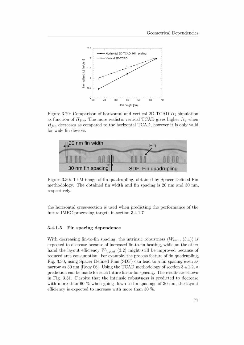
Geometrical Dependencies
0
0.5
1
1.5
2
2.5
10 20 30 40 50 60 70
Horizontal 2D-TCAD: Hfin scaling
Vertical 2D-TCAD
Nor
mal
ized
It2
[mA
/um
]
Fin height [nm]
Figure 3.29: Comparison of horizontal and vertical 2D-TCAD It2 simulationas function of Hfin. The more realistic vertical TCAD gives higher It2 whenHfin decreases as compared to the horizontal TCAD, however it is only validfor wide fin devices.
SDF: Fin quadrupling
20 nm fin width Fin
30 nm fin spacing
Figure 3.30: TEM image of fin quadrupling, obtained by Spacer Defined Finmethodology. The obtained fin width and fin spacing is 20 nm and 30 nm,respectively.
the horizontal cross-section is used when predicting the performance of thefuture IMEC processing targets in section 3.4.1.7.
3.4.1.5 Fin spacing dependence
With decreasing fin-to-fin spacing, the intrinsic robustness (Wintr, (3.1)) isexpected to decrease because of increased fin-to-fin heating, while on the otherhand the layout efficiency Wlayout (3.2) might still be improved because ofreduced area consumption. For example, the process feature of fin quadrupling,Fig. 3.30, using Spacer Defined Fins (SDF) can lead to a fin spacing even asnarrow as 30 nm [Rooy 06]. Using the TCAD methodology of section 3.4.1.2, aprediction can be made for such future fin-to-fin spacing. The results are shownin Fig. 3.31. Despite that the intrinsic robustness is predicted to decreasewith more than 60 % when going down to fin spacings of 30 nm, the layoutefficiency is expected to increase with more than 30 %.
77
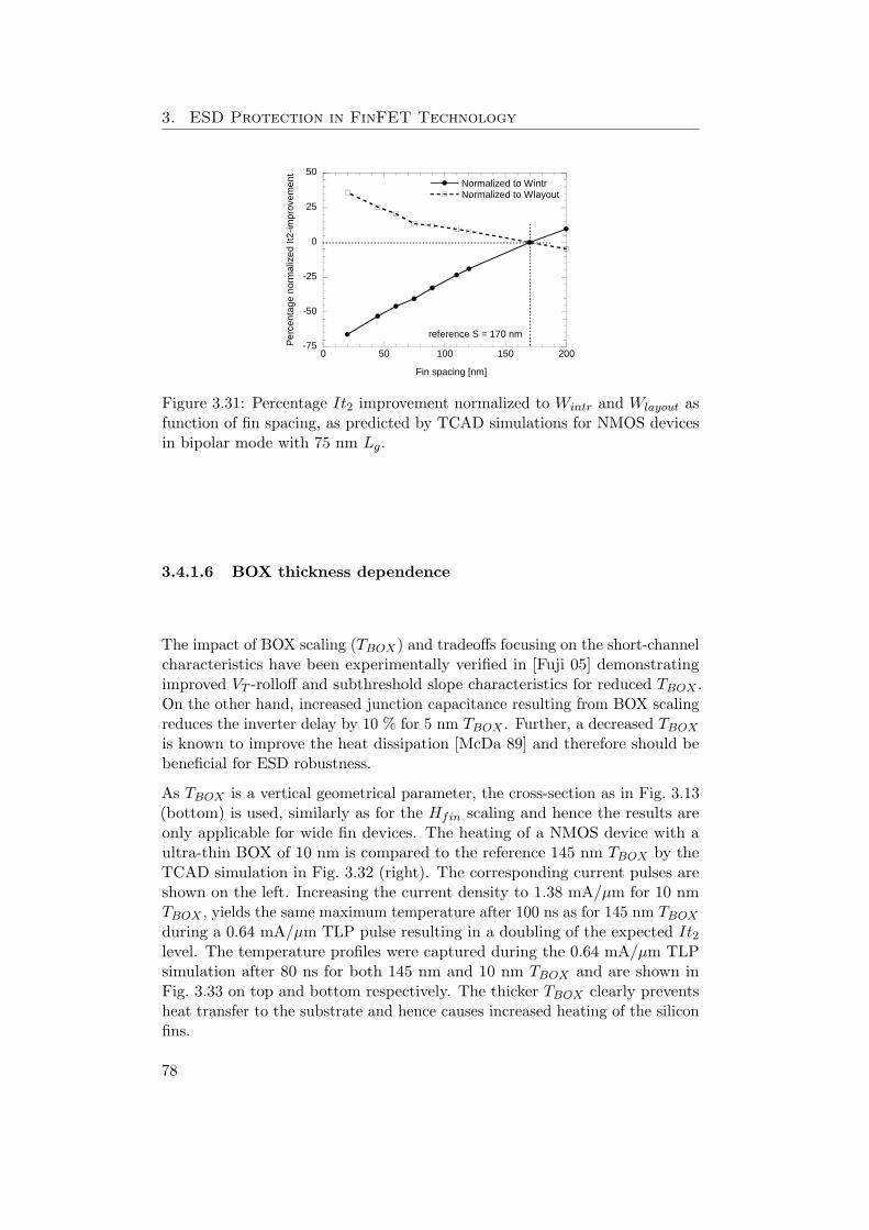
3. ESD Protection in FinFET Technology
-75
-50
-25
0
25
50
0 50 100 150 200
Normalized to WintrNormalized to Wlayout
Per
cent
age
norm
aliz
ed It
2-im
prov
emen
t
Fin spacing [nm]
reference S = 170 nm
Figure 3.31: Percentage It2 improvement normalized to Wintr and Wlayout asfunction of fin spacing, as predicted by TCAD simulations for NMOS devicesin bipolar mode with 75 nm Lg.
3.4.1.6 BOX thickness dependence
The impact of BOX scaling (TBOX) and tradeoffs focusing on the short-channelcharacteristics have been experimentally verified in [Fuji 05] demonstratingimproved VT -rolloff and subthreshold slope characteristics for reduced TBOX .On the other hand, increased junction capacitance resulting from BOX scalingreduces the inverter delay by 10 % for 5 nm TBOX . Further, a decreased TBOX
is known to improve the heat dissipation [McDa 89] and therefore should bebeneficial for ESD robustness.
As TBOX is a vertical geometrical parameter, the cross-section as in Fig. 3.13(bottom) is used, similarly as for the Hfin scaling and hence the results areonly applicable for wide fin devices. The heating of a NMOS device with aultra-thin BOX of 10 nm is compared to the reference 145 nm TBOX by theTCAD simulation in Fig. 3.32 (right). The corresponding current pulses areshown on the left. Increasing the current density to 1.38 mA/µm for 10 nmTBOX , yields the same maximum temperature after 100 ns as for 145 nm TBOX
during a 0.64 mA/µm TLP pulse resulting in a doubling of the expected It2level. The temperature profiles were captured during the 0.64 mA/µm TLPsimulation after 80 ns for both 145 nm and 10 nm TBOX and are shown inFig. 3.33 on top and bottom respectively. The thicker TBOX clearly preventsheat transfer to the substrate and hence causes increased heating of the siliconfins.
78
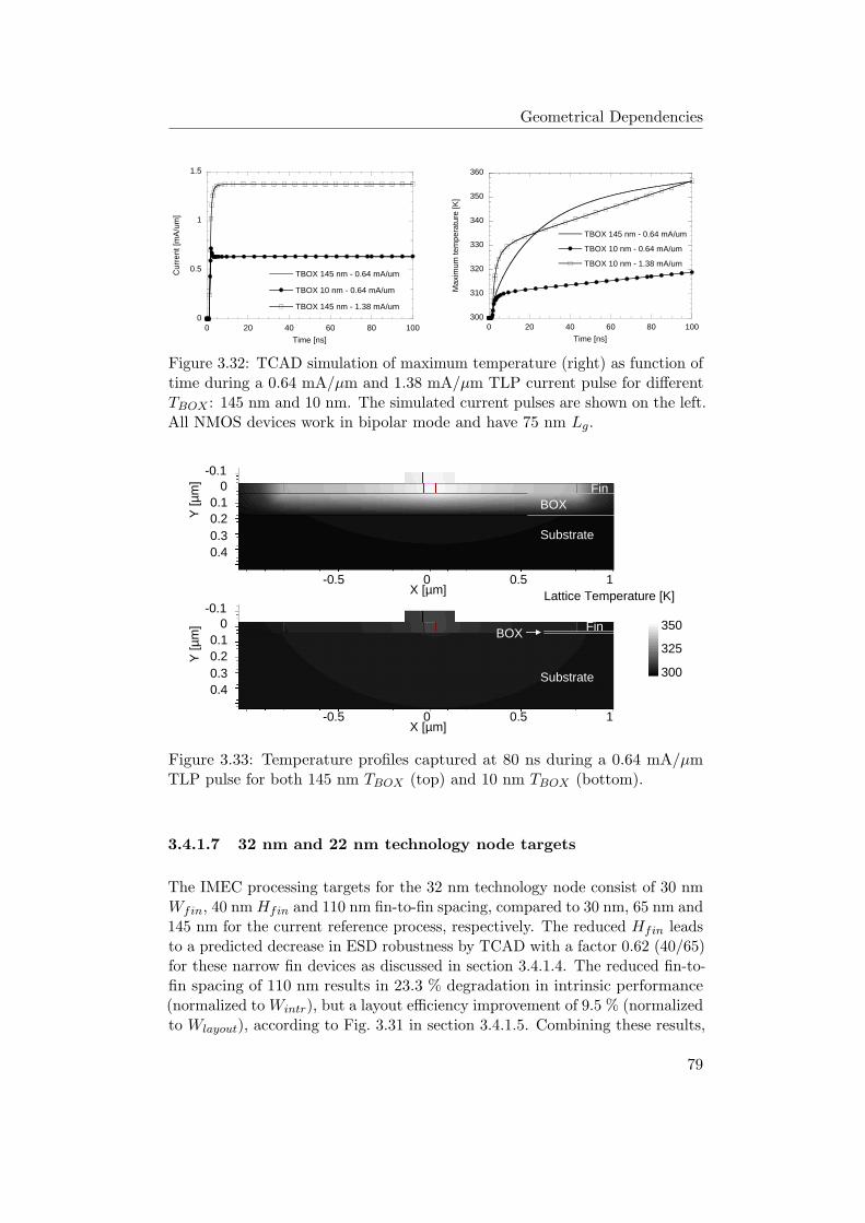
Geometrical Dependencies
0
0.5
1
1.5
0 20 40 60 80 100
TBOX 145 nm - 0.64 mA/um
TBOX 10 nm - 0.64 mA/um
TBOX 145 nm - 1.38 mA/um
Cur
rent
[mA
/um
]
Time [ns]
300
310
320
330
340
350
360
0 20 40 60 80 100
TBOX 145 nm - 0.64 mA/um
TBOX 10 nm - 0.64 mA/um
TBOX 10 nm - 1.38 mA/um
Max
imum
tem
pera
ture
[K]
Time [ns]
Figure 3.32: TCAD simulation of maximum temperature (right) as function oftime during a 0.64 mA/µm and 1.38 mA/µm TLP current pulse for differentTBOX : 145 nm and 10 nm. The simulated current pulses are shown on the left.All NMOS devices work in bipolar mode and have 75 nm Lg.
X [µm]
X [µm]
Y [µ
m]
Y [µ
m]
-0.5 0 0.5 1
-0.5 0 0.5 1
-0.10
0.10.20.30.4
-0.10
0.10.20.30.4
FinBOX
Substrate
FinBOX350
325
300
Lattice Temperature [K]
Substrate
Figure 3.33: Temperature profiles captured at 80 ns during a 0.64 mA/µmTLP pulse for both 145 nm TBOX (top) and 10 nm TBOX (bottom).
3.4.1.7 32 nm and 22 nm technology node targets
The IMEC processing targets for the 32 nm technology node consist of 30 nmWfin, 40 nm Hfin and 110 nm fin-to-fin spacing, compared to 30 nm, 65 nm and145 nm for the current reference process, respectively. The reduced Hfin leadsto a predicted decrease in ESD robustness by TCAD with a factor 0.62 (40/65)for these narrow fin devices as discussed in section 3.4.1.4. The reduced fin-to-fin spacing of 110 nm results in 23.3 % degradation in intrinsic performance(normalized to Wintr), but a layout efficiency improvement of 9.5 % (normalizedto Wlayout), according to Fig. 3.31 in section 3.4.1.5. Combining these results,
79
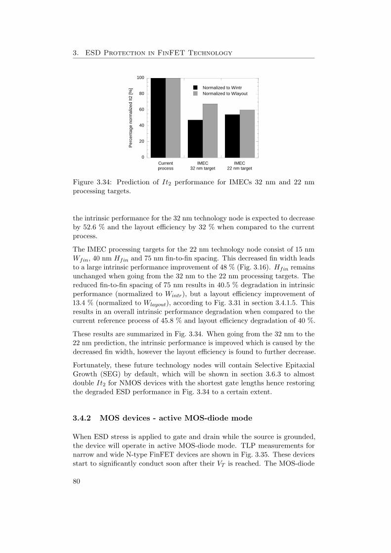
3. ESD Protection in FinFET Technology
0
20
40
60
80
100
Currentprocess
IMEC32 nm target
IMEC22 nm target
Normalized to Wintr
Per
cent
age
norm
aliz
ed It
2 [%
]
Normalized to Wlayout
Figure 3.34: Prediction of It2 performance for IMECs 32 nm and 22 nmprocessing targets.
the intrinsic performance for the 32 nm technology node is expected to decreaseby 52.6 % and the layout efficiency by 32 % when compared to the currentprocess.
The IMEC processing targets for the 22 nm technology node consist of 15 nmWfin, 40 nm Hfin and 75 nm fin-to-fin spacing. This decreased fin width leadsto a large intrinsic performance improvement of 48 % (Fig. 3.16). Hfin remainsunchanged when going from the 32 nm to the 22 nm processing targets. Thereduced fin-to-fin spacing of 75 nm results in 40.5 % degradation in intrinsicperformance (normalized to Wintr), but a layout efficiency improvement of13.4 % (normalized to Wlayout), according to Fig. 3.31 in section 3.4.1.5. Thisresults in an overall intrinsic performance degradation when compared to thecurrent reference process of 45.8 % and layout efficiency degradation of 40 %.
These results are summarized in Fig. 3.34. When going from the 32 nm to the22 nm prediction, the intrinsic performance is improved which is caused by thedecreased fin width, however the layout efficiency is found to further decrease.
Fortunately, these future technology nodes will contain Selective EpitaxialGrowth (SEG) by default, which will be shown in section 3.6.3 to almostdouble It2 for NMOS devices with the shortest gate lengths hence restoringthe degraded ESD performance in Fig. 3.34 to a certain extent.
3.4.2 MOS devices - active MOS-diode mode
When ESD stress is applied to gate and drain while the source is grounded,the device will operate in active MOS-diode mode. TLP measurements fornarrow and wide N-type FinFET devices are shown in Fig. 3.35. These devicesstart to significantly conduct soon after their VT is reached. The MOS-diode
80
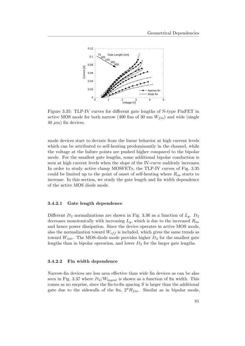
Geometrical Dependencies
0
0.02
0.04
0.06
0.08
0.1
0.12
0 1 2 3 4 5
Narrow finWide fin
Cur
rent
[A]
Voltage [V]
Gate Length (nm)75105
155355
955
Figure 3.35: TLP-IV curves for different gate lengths of N-type FinFET inactive MOS mode for both narrow (400 fins of 30 nm Wfin) and wide (single40 µm) fin devices.
mode devices start to deviate from the linear behavior at high current levelswhich can be attributed to self-heating predominantly in the channel, whilethe voltage at the failure points are pushed higher compared to the bipolarmode. For the smallest gate lengths, some additional bipolar conduction isseen at high current levels when the slope of the IV-curve suddenly increases.In order to study active clamp MOSFETs, the TLP-IV curves of Fig. 3.35could be limited up to the point of onset of self-heating where Ron starts toincrease. In this section, we study the gate length and fin width dependenceof the active MOS diode mode.
3.4.2.1 Gate length dependence
Different It2 normalizations are shown in Fig. 3.36 as a function of Lg. It2decreases monotonically with increasing Lg, which is due to the increased Ron
and hence power dissipation. Since the device operates in active MOS mode,also the normalization toward Weff is included, which gives the same trends astoward Wintr. The MOS-diode mode provides higher It2 for the smallest gatelengths than in bipolar operation, and lower It2 for the larger gate lengths.
3.4.2.2 Fin width dependence
Narrow-fin devices are less area effective than wide fin devices as can be alsoseen in Fig. 3.37 where It2/Wlayout is shown as a function of fin width. Thiscomes as no surprise, since the fin-to-fin spacing S is larger than the additionalgate due to the sidewalls of the fin, 2*Hfin. Similar as in bipolar mode,
81
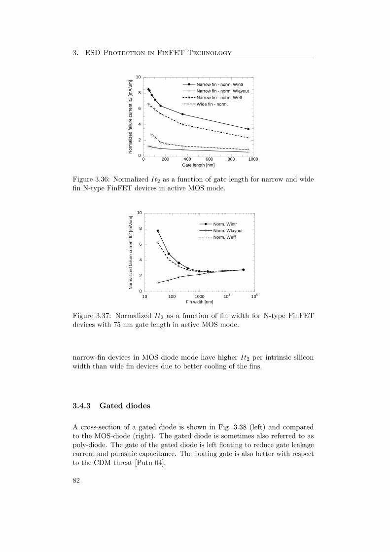
3. ESD Protection in FinFET Technology
0
2
4
6
8
10
0 200 400 600 800 1000
Narrow fin - norm. Wintr
Narrow fin - norm. Wlayout
Narrow fin - norm. Weff
Wide fin - norm.
Nor
mal
ized
failu
re c
urre
nt It
2 [m
A/u
m]
Gate length [nm]
Figure 3.36: Normalized It2 as a function of gate length for narrow and widefin N-type FinFET devices in active MOS mode.
0
2
4
6
8
10
10 100 1000 104 105
Norm. Wintr
Norm. Wlayout
Norm. Weff
Nor
mal
ized
failu
re c
urre
nt It
2 [m
A/u
m]
Fin width [nm]
Figure 3.37: Normalized It2 as a function of fin width for N-type FinFETdevices with 75 nm gate length in active MOS mode.
narrow-fin devices in MOS diode mode have higher It2 per intrinsic siliconwidth than wide fin devices due to better cooling of the fins.
3.4.3 Gated diodes
A cross-section of a gated diode is shown in Fig. 3.38 (left) and comparedto the MOS-diode (right). The gated diode is sometimes also referred to aspoly-diode. The gate of the gated diode is left floating to reduce gate leakagecurrent and parasitic capacitance. The floating gate is also better with respectto the CDM threat [Putn 04].
82
Geometrical Dependencies
i N+N+i N+P+
MOS diodeGated diodeA CA C
Figure 3.38: Cross-section of gated diode (left) compared to MOS diode (right).
0
0.05
0.1
0.15
0.2
0.25
0.3
0 1 2 3 4
Gated diode
MOS diodeCur
rent
[A]
Voltage [V]
Gate Length (nm)155355
555755
955
Figure 3.39: TLP-IV curves for different gate lengths of gated diodes incomparison with MOS diode mode. The devices have a fin width of 30 nm and400 fins in parallel.
3.4.3.1 Gate length dependence
TLP-IV curves of gated diodes as a function of Lg are compared in Fig. 3.39with the MOS diode mode. It is clear that gated diodes exhibit an improvedIt2 and Ron, which is optimal for smallest Lg. Note that the gate lengths usedfor the gated diodes are larger than what can be used for the MOS devices(see Fig. 3.35) to accommodate for the N+ and P+ doping overlap on the gatedue to mask misalignment.
3.4.3.2 Fin width dependence
When increasing Wfin, It2 normalized per intrinsic silicon width decreaseswhile it increases when considering layout Fig. 3.40, similarly as for the MOSdiode mode. Since the leakage current is small for the gated diodes due thelarger gate lengths needed, the optimum diode configuration in terms of ESDperformance and area consumption is a wide fin diode with the smallest gatelength possible.
83
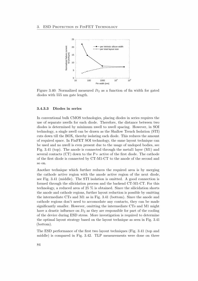
3. ESD Protection in FinFET Technology
0
5
10
15
20
25
10 100 1000 104 105
per intrinsic silicon widthper total layout size
Nor
mal
ized
failu
re c
urre
ntIt2
[mA
/µm
]
Fin width [nm]
Figure 3.40: Normalized measured It2 as a function of fin width for gateddiodes with 555 nm gate length.
3.4.3.3 Diodes in series
In conventional bulk CMOS technologies, placing diodes in series requires theuse of separate nwells for each diode. Therefore, the distance between twodiodes is determined by minimum nwell to nwell spacing. However, in SOItechnology, a single nwell can be drawn as the Shallow Trench Isolation (STI)cuts down till the BOX, thereby isolating each diode. This reduces the amountof required space. In FinFET SOI technology, the same layout technique canbe used and no nwell is even present due to the usage of undoped bodies, seeFig. 3.41 (top). The anode is connected through the metal1 layer (M1) andseveral contacts (CT) down to the P+ active of the first diode. The cathodeof the first diode is connected by CT-M1-CT to the anode of the second andso on.
Another technique which further reduces the required area is by mergingthe cathode active region with the anode active region of the next diode,see Fig. 3.41 (middle). The STI isolation is omitted. A good connection isformed through the silicidation process and the backend CT-M1-CT. For thistechnology, a reduced area of 25 % is obtained. Since the silicidation shortsthe anode and cathode regions, further layout reduction is possible by omittingthe intermediate CTs and M1 as in Fig. 3.41 (bottom). Since the anode andcathode regions don’t need to accomodate any contacts, they can be madesignificantly smaller. However, omitting the intermediate CTs and M1 mighthave a drastic influence on It2 as they are responsible for part of the coolingof the device during ESD stress. More investigation is required to determinethe optimal layout strategy based on the layout technique as seen in Fig. 3.41(bottom).
The ESD performance of the first two layout techniques (Fig. 3.41 (top andmiddle) is compared in Fig. 3.42. TLP measurements were done on three
84
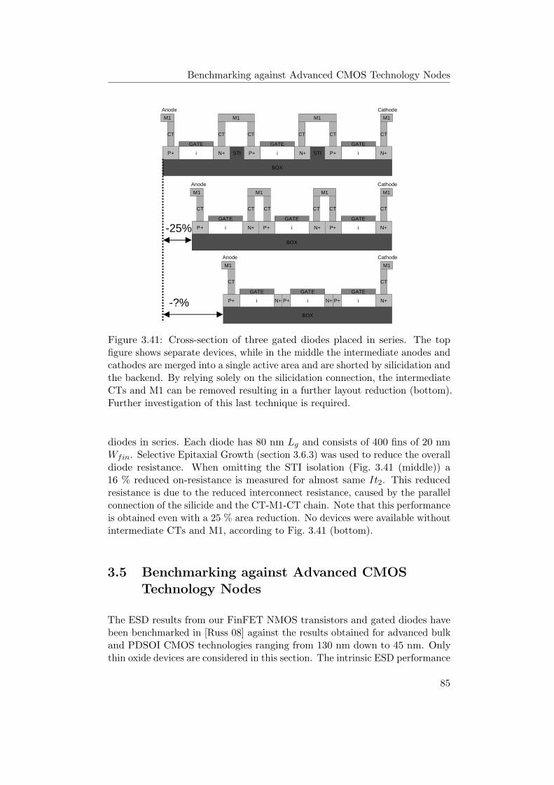
Benchmarking against Advanced CMOS Technology Nodes
i
GATE
N+P+
Cathode
i
GATE
N+P+i
GATE
N+P+ STI STI
Anode
CT CT CT CT CT CT
M1 M1 M1 M1
BOX
-25%
i
GATE
N+P+
Cathode
i
GATE
N+P+
Anode
CT CT
M1 M1
P+i
GATE
N+
BOX
-?%
i
GATE
N+P+
Cathode
i
GATE
N+P+i
GATE
N+P+
Anode
CT CT
M1 M1
BOX
CT CT
M1
CT CT
M1
Figure 3.41: Cross-section of three gated diodes placed in series. The topfigure shows separate devices, while in the middle the intermediate anodes andcathodes are merged into a single active area and are shorted by silicidation andthe backend. By relying solely on the silicidation connection, the intermediateCTs and M1 can be removed resulting in a further layout reduction (bottom).Further investigation of this last technique is required.
diodes in series. Each diode has 80 nm Lg and consists of 400 fins of 20 nmWfin. Selective Epitaxial Growth (section 3.6.3) was used to reduce the overalldiode resistance. When omitting the STI isolation (Fig. 3.41 (middle)) a16 % reduced on-resistance is measured for almost same It2. This reducedresistance is due to the reduced interconnect resistance, caused by the parallelconnection of the silicide and the CT-M1-CT chain. Note that this performanceis obtained even with a 25 % area reduction. No devices were available withoutintermediate CTs and M1, according to Fig. 3.41 (bottom).
3.5 Benchmarking against Advanced CMOSTechnology Nodes
The ESD results from our FinFET NMOS transistors and gated diodes havebeen benchmarked in [Russ 08] against the results obtained for advanced bulkand PDSOI CMOS technologies ranging from 130 nm down to 45 nm. Onlythin oxide devices are considered in this section. The intrinsic ESD performance
85
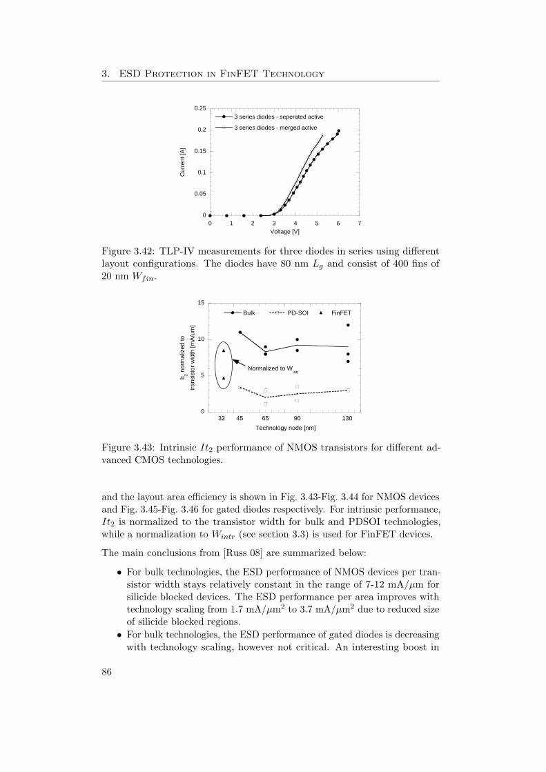
3. ESD Protection in FinFET Technology
0
0.05
0.1
0.15
0.2
0.25
0 1 2 3 4 5 6 7
3 series diodes - seperated active
3 series diodes - merged active
Cur
rent
[A]
Voltage [V]
Figure 3.42: TLP-IV measurements for three diodes in series using differentlayout configurations. The diodes have 80 nm Lg and consist of 400 fins of20 nm Wfin.
0
5
10
15
32 45 65 90 130
Bulk PD-SOI FinFET
It 2 nor
mal
ized
to
tran
sist
or w
idth
[mA
/um
]
Technology node [nm]
Normalized to Wintr
Figure 3.43: Intrinsic It2 performance of NMOS transistors for different ad-vanced CMOS technologies.
and the layout area efficiency is shown in Fig. 3.43-Fig. 3.44 for NMOS devicesand Fig. 3.45-Fig. 3.46 for gated diodes respectively. For intrinsic performance,It2 is normalized to the transistor width for bulk and PDSOI technologies,while a normalization to Wintr (see section 3.3) is used for FinFET devices.
The main conclusions from [Russ 08] are summarized below:
• For bulk technologies, the ESD performance of NMOS devices per tran-sistor width stays relatively constant in the range of 7-12 mA/µm forsilicide blocked devices. The ESD performance per area improves withtechnology scaling from 1.7 mA/µm2 to 3.7 mA/µm2 due to reduced sizeof silicide blocked regions.
• For bulk technologies, the ESD performance of gated diodes is decreasingwith technology scaling, however not critical. An interesting boost in
86
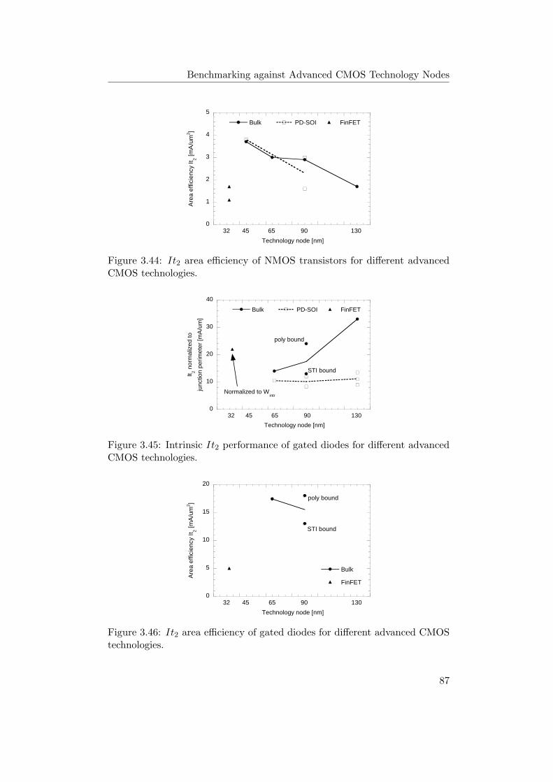
Benchmarking against Advanced CMOS Technology Nodes
0
1
2
3
4
5
32 45 65 90 130
Bulk PD-SOI FinFET
Are
a ef
ficie
ncy
It 2 [mA
/um
2 ]
Technology node [nm]
Figure 3.44: It2 area efficiency of NMOS transistors for different advancedCMOS technologies.
0
10
20
30
40
32 45 65 90 130
Bulk PD-SOI FinFET
It 2 nor
mal
ized
to
junc
tion
perim
eter
[mA
/um
]
Technology node [nm]
Normalized to Wintr
STI bound
poly bound
Figure 3.45: Intrinsic It2 performance of gated diodes for different advancedCMOS technologies.
0
5
10
15
20
32 45 65 90 130
Bulk
FinFET
Are
a ef
ficie
ncy
It 2 [mA
/um
2 ]
Technology node [nm]
STI bound
poly bound
Figure 3.46: It2 area efficiency of gated diodes for different advanced CMOStechnologies.
87
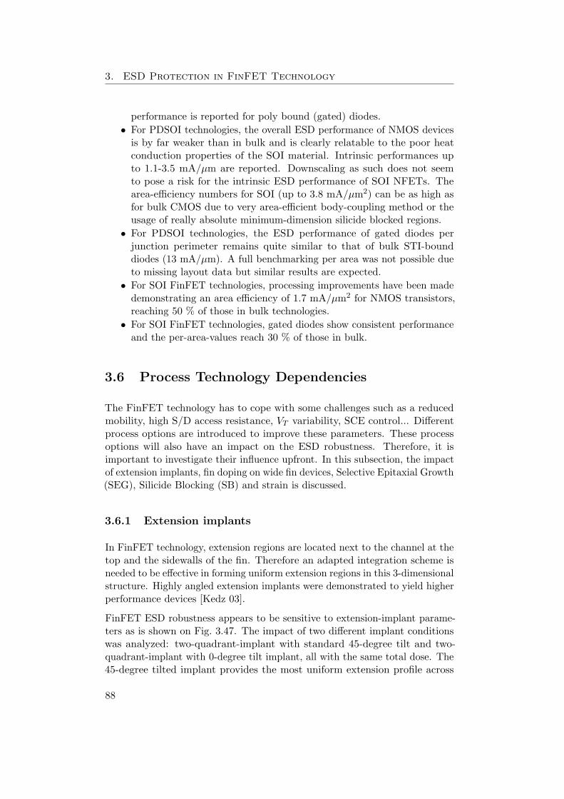
3. ESD Protection in FinFET Technology
performance is reported for poly bound (gated) diodes.• For PDSOI technologies, the overall ESD performance of NMOS devices
is by far weaker than in bulk and is clearly relatable to the poor heatconduction properties of the SOI material. Intrinsic performances upto 1.1-3.5 mA/µm are reported. Downscaling as such does not seemto pose a risk for the intrinsic ESD performance of SOI NFETs. Thearea-efficiency numbers for SOI (up to 3.8 mA/µm2) can be as high asfor bulk CMOS due to very area-efficient body-coupling method or theusage of really absolute minimum-dimension silicide blocked regions.
• For PDSOI technologies, the ESD performance of gated diodes perjunction perimeter remains quite similar to that of bulk STI-bounddiodes (13 mA/µm). A full benchmarking per area was not possible dueto missing layout data but similar results are expected.
• For SOI FinFET technologies, processing improvements have been madedemonstrating an area efficiency of 1.7 mA/µm2 for NMOS transistors,reaching 50 % of those in bulk technologies.
• For SOI FinFET technologies, gated diodes show consistent performanceand the per-area-values reach 30 % of those in bulk.
3.6 Process Technology Dependencies
The FinFET technology has to cope with some challenges such as a reducedmobility, high S/D access resistance, VT variability, SCE control... Differentprocess options are introduced to improve these parameters. These processoptions will also have an impact on the ESD robustness. Therefore, it isimportant to investigate their influence upfront. In this subsection, the impactof extension implants, fin doping on wide fin devices, Selective Epitaxial Growth(SEG), Silicide Blocking (SB) and strain is discussed.
3.6.1 Extension implants
In FinFET technology, extension regions are located next to the channel at thetop and the sidewalls of the fin. Therefore an adapted integration scheme isneeded to be effective in forming uniform extension regions in this 3-dimensionalstructure. Highly angled extension implants were demonstrated to yield higherperformance devices [Kedz 03].
FinFET ESD robustness appears to be sensitive to extension-implant parame-ters as is shown on Fig. 3.47. The impact of two different implant conditionswas analyzed: two-quadrant-implant with standard 45-degree tilt and two-quadrant-implant with 0-degree tilt implant, all with the same total dose. The45-degree tilted implant provides the most uniform extension profile across
88
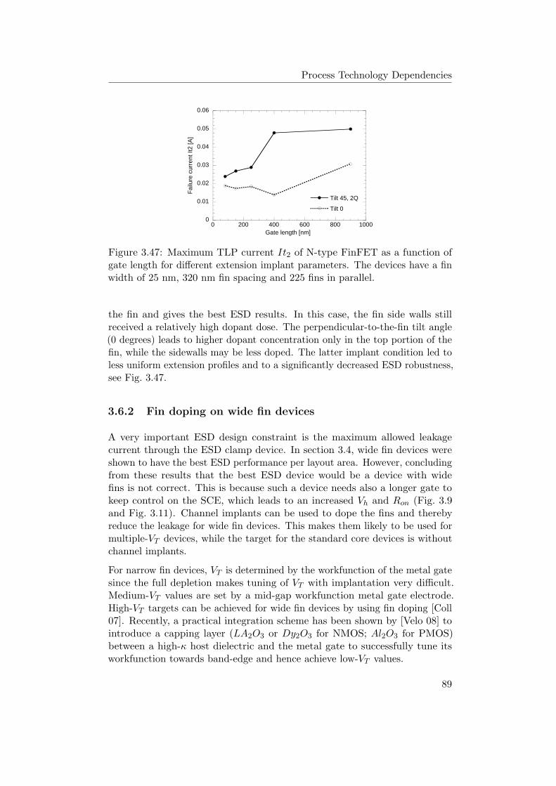
Process Technology Dependencies
0
0.01
0.02
0.03
0.04
0.05
0.06
0 200 400 600 800 1000
Tilt 45, 2Q
Tilt 0
Fai
lure
cur
rent
It2
[A]
Gate length [nm]
Figure 3.47: Maximum TLP current It2 of N-type FinFET as a function ofgate length for different extension implant parameters. The devices have a finwidth of 25 nm, 320 nm fin spacing and 225 fins in parallel.
the fin and gives the best ESD results. In this case, the fin side walls stillreceived a relatively high dopant dose. The perpendicular-to-the-fin tilt angle(0 degrees) leads to higher dopant concentration only in the top portion of thefin, while the sidewalls may be less doped. The latter implant condition led toless uniform extension profiles and to a significantly decreased ESD robustness,see Fig. 3.47.
3.6.2 Fin doping on wide fin devices
A very important ESD design constraint is the maximum allowed leakagecurrent through the ESD clamp device. In section 3.4, wide fin devices wereshown to have the best ESD performance per layout area. However, concludingfrom these results that the best ESD device would be a device with widefins is not correct. This is because such a device needs also a longer gate tokeep control on the SCE, which leads to an increased Vh and Ron (Fig. 3.9and Fig. 3.11). Channel implants can be used to dope the fins and therebyreduce the leakage for wide fin devices. This makes them likely to be used formultiple-VT devices, while the target for the standard core devices is withoutchannel implants.
For narrow fin devices, VT is determined by the workfunction of the metal gatesince the full depletion makes tuning of VT with implantation very difficult.Medium-VT values are set by a mid-gap workfunction metal gate electrode.High-VT targets can be achieved for wide fin devices by using fin doping [Coll07]. Recently, a practical integration scheme has been shown by [Velo 08] tointroduce a capping layer (LA2O3 or Dy2O3 for NMOS; Al2O3 for PMOS)between a high-κ host dielectric and the metal gate to successfully tune itsworkfunction towards band-edge and hence achieve low-VT values.
89
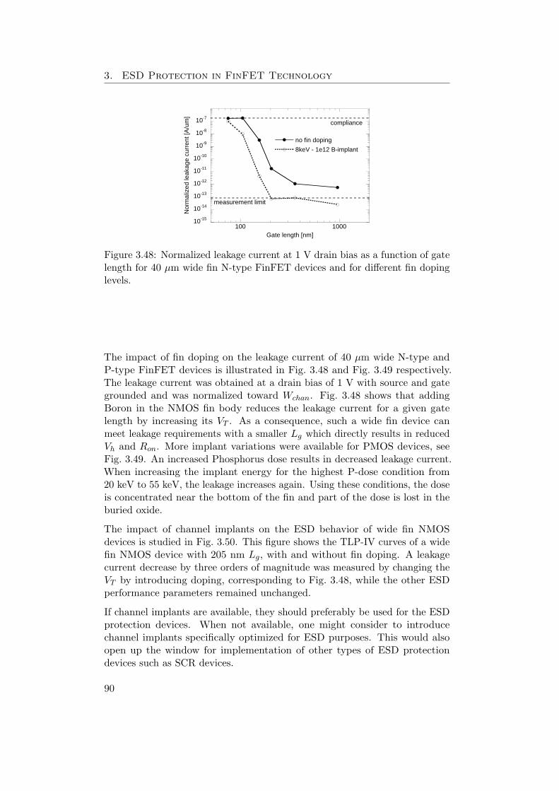
3. ESD Protection in FinFET Technology
10-15
10-14
10-13
10-12
10-11
10-10
10-9
10-8
10-7
100 1000
no fin doping
8keV - 1e12 B-implant
Nor
mal
ized
leak
age
curr
ent [
A/u
m]
Gate length [nm]
measurement limit
compliance
Figure 3.48: Normalized leakage current at 1 V drain bias as a function of gatelength for 40 µm wide fin N-type FinFET devices and for different fin dopinglevels.
The impact of fin doping on the leakage current of 40 µm wide N-type andP-type FinFET devices is illustrated in Fig. 3.48 and Fig. 3.49 respectively.The leakage current was obtained at a drain bias of 1 V with source and gategrounded and was normalized toward Wchan. Fig. 3.48 shows that addingBoron in the NMOS fin body reduces the leakage current for a given gatelength by increasing its VT . As a consequence, such a wide fin device canmeet leakage requirements with a smaller Lg which directly results in reducedVh and Ron. More implant variations were available for PMOS devices, seeFig. 3.49. An increased Phosphorus dose results in decreased leakage current.When increasing the implant energy for the highest P-dose condition from20 keV to 55 keV, the leakage increases again. Using these conditions, the doseis concentrated near the bottom of the fin and part of the dose is lost in theburied oxide.
The impact of channel implants on the ESD behavior of wide fin NMOSdevices is studied in Fig. 3.50. This figure shows the TLP-IV curves of a widefin NMOS device with 205 nm Lg, with and without fin doping. A leakagecurrent decrease by three orders of magnitude was measured by changing theVT by introducing doping, corresponding to Fig. 3.48, while the other ESDperformance parameters remained unchanged.
If channel implants are available, they should preferably be used for the ESDprotection devices. When not available, one might consider to introducechannel implants specifically optimized for ESD purposes. This would alsoopen up the window for implementation of other types of ESD protectiondevices such as SCR devices.
90
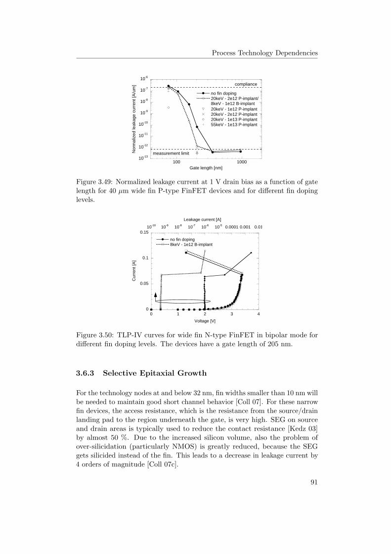
Process Technology Dependencies
10-13
10-12
10-11
10-10
10-9
10-8
10-7
10-6
100 1000
no fin doping20keV - 2e12 P-implant/8keV - 1e12 B-implant20keV - 1e12 P-implant20keV - 2e12 P-implant20keV - 1e13 P-implant55keV - 1e13 P-implant
Nor
mal
ized
leak
age
curr
ent [
A/u
m]
Gate length [nm]
measurement limit
compliance
Figure 3.49: Normalized leakage current at 1 V drain bias as a function of gatelength for 40 µm wide fin P-type FinFET devices and for different fin dopinglevels.
0
0.05
0.1
0.15
0 1 2 3 4
no fin doping8keV - 1e12 B-implant
10-10 10-9 10-8 10-7 10-6 10-5 0.0001 0.001 0.01
Cur
rent
[A]
Voltage [V]
Leakage current [A]
Figure 3.50: TLP-IV curves for wide fin N-type FinFET in bipolar mode fordifferent fin doping levels. The devices have a gate length of 205 nm.
3.6.3 Selective Epitaxial Growth
For the technology nodes at and below 32 nm, fin widths smaller than 10 nm willbe needed to maintain good short channel behavior [Coll 07]. For these narrowfin devices, the access resistance, which is the resistance from the source/drainlanding pad to the region underneath the gate, is very high. SEG on sourceand drain areas is typically used to reduce the contact resistance [Kedz 03]by almost 50 %. Due to the increased silicon volume, also the problem ofover-silicidation (particularly NMOS) is greatly reduced, because the SEGgets silicided instead of the fin. This leads to a decrease in leakage current by4 orders of magnitude [Coll 07c].
91
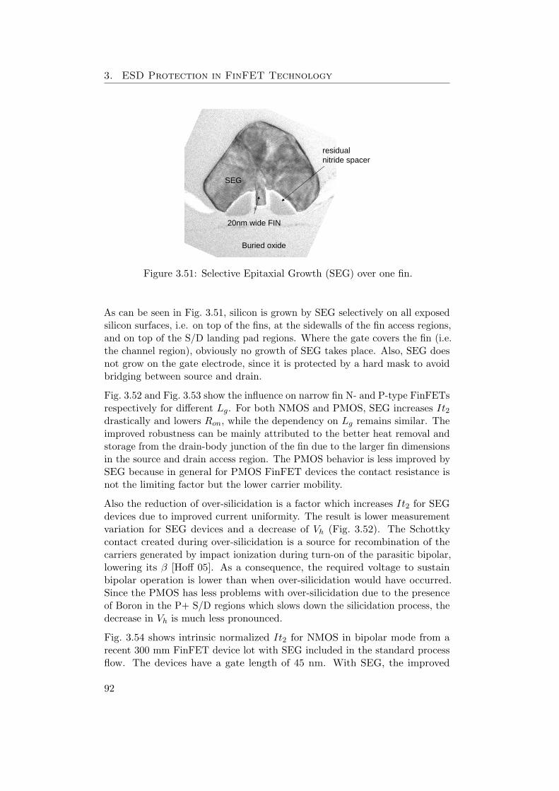
3. ESD Protection in FinFET Technology
SEG
20nm wide FIN
residualnitride spacer
Buried oxide
Figure 3.51: Selective Epitaxial Growth (SEG) over one fin.
As can be seen in Fig. 3.51, silicon is grown by SEG selectively on all exposedsilicon surfaces, i.e. on top of the fins, at the sidewalls of the fin access regions,and on top of the S/D landing pad regions. Where the gate covers the fin (i.e.the channel region), obviously no growth of SEG takes place. Also, SEG doesnot grow on the gate electrode, since it is protected by a hard mask to avoidbridging between source and drain.
Fig. 3.52 and Fig. 3.53 show the influence on narrow fin N- and P-type FinFETsrespectively for different Lg. For both NMOS and PMOS, SEG increases It2drastically and lowers Ron, while the dependency on Lg remains similar. Theimproved robustness can be mainly attributed to the better heat removal andstorage from the drain-body junction of the fin due to the larger fin dimensionsin the source and drain access region. The PMOS behavior is less improved bySEG because in general for PMOS FinFET devices the contact resistance isnot the limiting factor but the lower carrier mobility.
Also the reduction of over-silicidation is a factor which increases It2 for SEGdevices due to improved current uniformity. The result is lower measurementvariation for SEG devices and a decrease of Vh (Fig. 3.52). The Schottkycontact created during over-silicidation is a source for recombination of thecarriers generated by impact ionization during turn-on of the parasitic bipolar,lowering its β [Hoff 05]. As a consequence, the required voltage to sustainbipolar operation is lower than when over-silicidation would have occurred.Since the PMOS has less problems with over-silicidation due to the presenceof Boron in the P+ S/D regions which slows down the silicidation process, thedecrease in Vh is much less pronounced.
Fig. 3.54 shows intrinsic normalized It2 for NMOS in bipolar mode from arecent 300 mm FinFET device lot with SEG included in the standard processflow. The devices have a gate length of 45 nm. With SEG, the improved
92
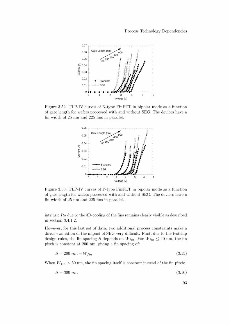
Process Technology Dependencies
0
0.01
0.02
0.03
0.04
0.05
0.06
0.07
0 1 2 3 4 5 6
Standard
SEG
Cur
rent
[A]
Voltage [V]
Gate Length (nm)
80150
250400
900
Figure 3.52: TLP-IV curves of N-type FinFET in bipolar mode as a functionof gate length for wafers processed with and without SEG. The devices have afin width of 25 nm and 225 fins in parallel.
0
0.01
0.02
0.03
0.04
0.05
0.06
0 1 2 3 4 5 6 7
Standard
SEG
Cur
rent
[A]
Voltage [V]
Gate Length (nm)
80150
250400
900
Figure 3.53: TLP-IV curves of P-type FinFET in bipolar mode as a functionof gate length for wafers processed with and without SEG. The devices have afin width of 25 nm and 225 fins in parallel.
intrinsic It2 due to the 3D-cooling of the fins remains clearly visible as describedin section 3.4.1.2.
However, for this last set of data, two additional process constraints make adirect evaluation of the impact of SEG very difficult. First, due to the testchipdesign rules, the fin spacing S depends on Wfin. For Wfin ≤ 40 nm, the finpitch is constant at 200 nm, giving a fin spacing of:
S = 200 nm−Wfin (3.15)
When Wfin > 50 nm, the fin spacing itself is constant instead of the fin pitch:
S = 300 nm (3.16)
93
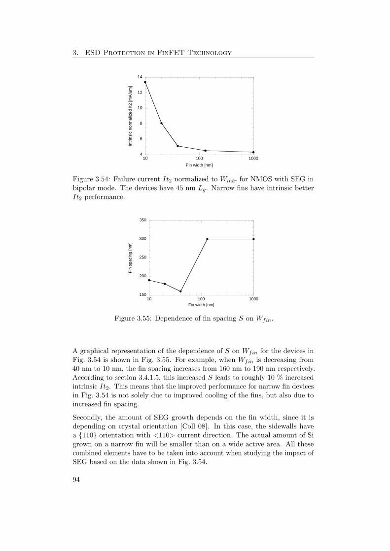
3. ESD Protection in FinFET Technology
4
6
8
10
12
14
10 100 1000
Intr
insi
c no
rmal
ized
It2
[mA
/um
]
Fin width [nm]
Figure 3.54: Failure current It2 normalized to Wintr for NMOS with SEG inbipolar mode. The devices have 45 nm Lg. Narrow fins have intrinsic betterIt2 performance.
150
200
250
300
350
10 100 1000
Fin
spa
cing
[nm
]
Fin width [nm]
Figure 3.55: Dependence of fin spacing S on Wfin.
A graphical representation of the dependence of S on Wfin for the devices inFig. 3.54 is shown in Fig. 3.55. For example, when Wfin is decreasing from40 nm to 10 nm, the fin spacing increases from 160 nm to 190 nm respectively.According to section 3.4.1.5, this increased S leads to roughly 10 % increasedintrinsic It2. This means that the improved performance for narrow fin devicesin Fig. 3.54 is not solely due to improved cooling of the fins, but also due toincreased fin spacing.
Secondly, the amount of SEG growth depends on the fin width, since it isdepending on crystal orientation [Coll 08]. In this case, the sidewalls havea 110 orientation with <110> current direction. The actual amount of Sigrown on a narrow fin will be smaller than on a wide active area. All thesecombined elements have to be taken into account when studying the impact ofSEG based on the data shown in Fig. 3.54.
94
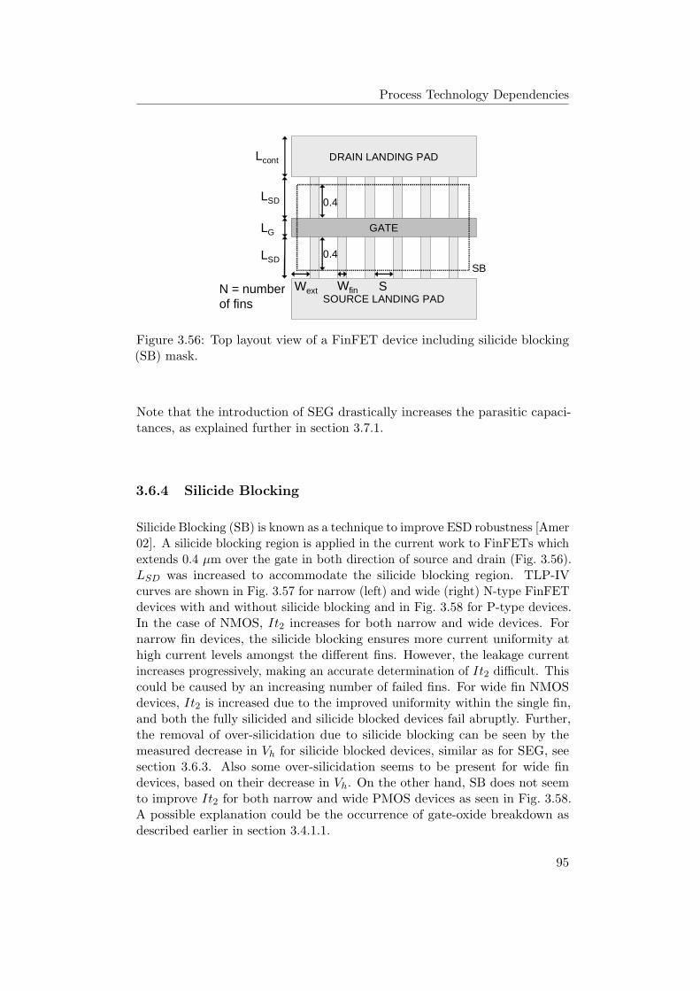
Process Technology Dependencies
GATE
SOURCE LANDING PAD
DRAIN LANDING PAD
LG
LSD
Lcont
Wext Wfin SN = numberof fins
LSD
0.4
0.4SB
Figure 3.56: Top layout view of a FinFET device including silicide blocking(SB) mask.
Note that the introduction of SEG drastically increases the parasitic capaci-tances, as explained further in section 3.7.1.
3.6.4 Silicide Blocking
Silicide Blocking (SB) is known as a technique to improve ESD robustness [Amer02]. A silicide blocking region is applied in the current work to FinFETs whichextends 0.4 µm over the gate in both direction of source and drain (Fig. 3.56).LSD was increased to accommodate the silicide blocking region. TLP-IVcurves are shown in Fig. 3.57 for narrow (left) and wide (right) N-type FinFETdevices with and without silicide blocking and in Fig. 3.58 for P-type devices.In the case of NMOS, It2 increases for both narrow and wide devices. Fornarrow fin devices, the silicide blocking ensures more current uniformity athigh current levels amongst the different fins. However, the leakage currentincreases progressively, making an accurate determination of It2 difficult. Thiscould be caused by an increasing number of failed fins. For wide fin NMOSdevices, It2 is increased due to the improved uniformity within the single fin,and both the fully silicided and silicide blocked devices fail abruptly. Further,the removal of over-silicidation due to silicide blocking can be seen by themeasured decrease in Vh for silicide blocked devices, similar as for SEG, seesection 3.6.3. Also some over-silicidation seems to be present for wide findevices, based on their decrease in Vh. On the other hand, SB does not seemto improve It2 for both narrow and wide PMOS devices as seen in Fig. 3.58.A possible explanation could be the occurrence of gate-oxide breakdown asdescribed earlier in section 3.4.1.1.
95
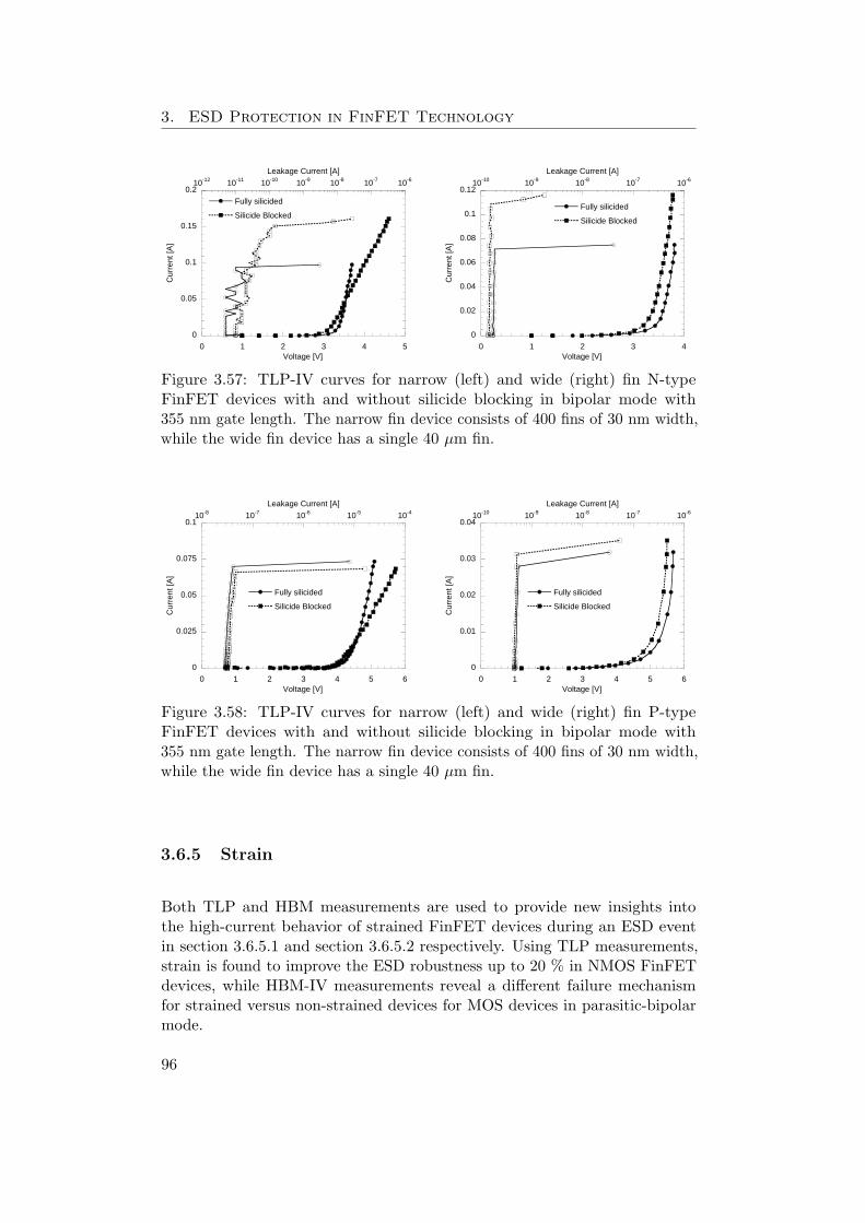
3. ESD Protection in FinFET Technology
0
0.05
0.1
0.15
0.2
0 1 2 3 4 5
10-12 10-11 10-10 10-9 10-8 10-7 10-6
Fully silicided
Silicide Blocked
Cur
rent
[A]
Voltage [V]
Leakage Current [A]
0
0.02
0.04
0.06
0.08
0.1
0.12
0 1 2 3 4
10-10 10-9 10-8 10-7 10-6
Fully silicided
Silicide Blocked
Cur
rent
[A]
Voltage [V]
Leakage Current [A]
Figure 3.57: TLP-IV curves for narrow (left) and wide (right) fin N-typeFinFET devices with and without silicide blocking in bipolar mode with355 nm gate length. The narrow fin device consists of 400 fins of 30 nm width,while the wide fin device has a single 40 µm fin.
0
0.025
0.05
0.075
0.1
0 1 2 3 4 5 6
10-8 10-7 10-6 10-5 10-4
Fully silicided
Silicide Blocked
Cur
rent
[A]
Voltage [V]
Leakage Current [A]
0
0.01
0.02
0.03
0.04
0 1 2 3 4 5 6
10-10 10-9 10-8 10-7 10-6
Fully silicided
Silicide Blocked
Cur
rent
[A]
Voltage [V]
Leakage Current [A]
Figure 3.58: TLP-IV curves for narrow (left) and wide (right) fin P-typeFinFET devices with and without silicide blocking in bipolar mode with355 nm gate length. The narrow fin device consists of 400 fins of 30 nm width,while the wide fin device has a single 40 µm fin.
3.6.5 Strain
Both TLP and HBM measurements are used to provide new insights intothe high-current behavior of strained FinFET devices during an ESD eventin section 3.6.5.1 and section 3.6.5.2 respectively. Using TLP measurements,strain is found to improve the ESD robustness up to 20 % in NMOS FinFETdevices, while HBM-IV measurements reveal a different failure mechanismfor strained versus non-strained devices for MOS devices in parasitic-bipolarmode.
96
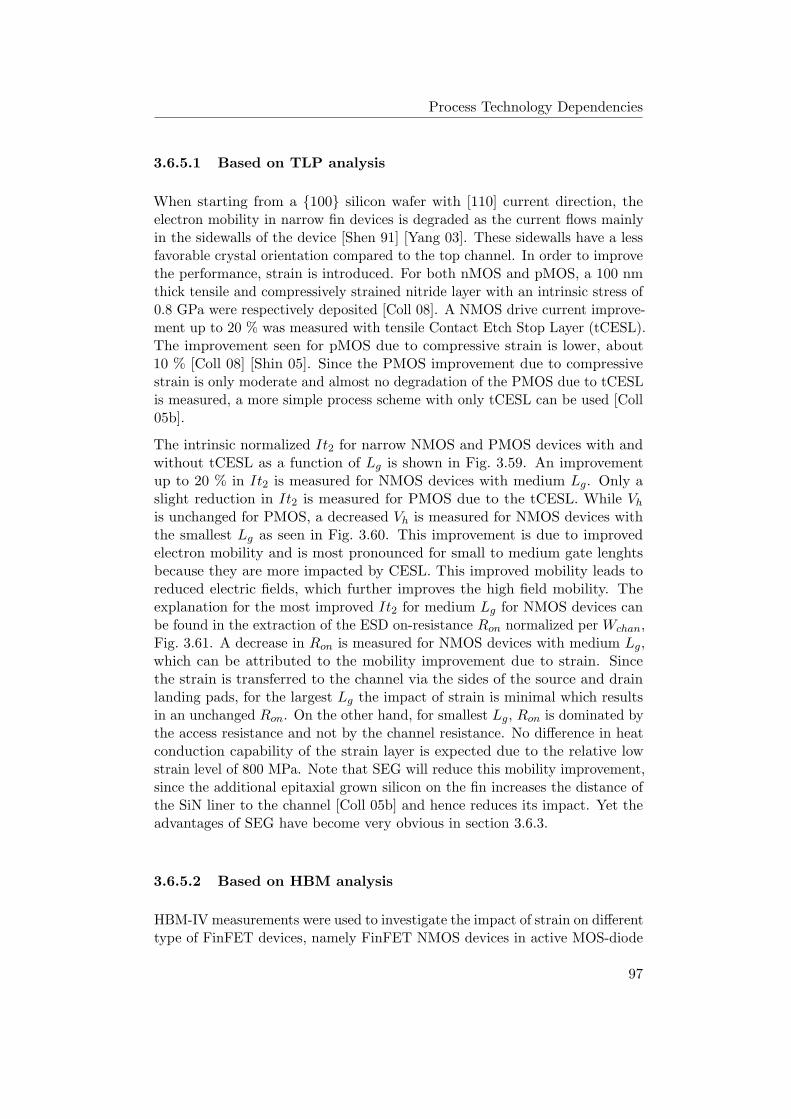
Process Technology Dependencies
3.6.5.1 Based on TLP analysis
When starting from a 100 silicon wafer with [110] current direction, theelectron mobility in narrow fin devices is degraded as the current flows mainlyin the sidewalls of the device [Shen 91] [Yang 03]. These sidewalls have a lessfavorable crystal orientation compared to the top channel. In order to improvethe performance, strain is introduced. For both nMOS and pMOS, a 100 nmthick tensile and compressively strained nitride layer with an intrinsic stress of0.8 GPa were respectively deposited [Coll 08]. A NMOS drive current improve-ment up to 20 % was measured with tensile Contact Etch Stop Layer (tCESL).The improvement seen for pMOS due to compressive strain is lower, about10 % [Coll 08] [Shin 05]. Since the PMOS improvement due to compressivestrain is only moderate and almost no degradation of the PMOS due to tCESLis measured, a more simple process scheme with only tCESL can be used [Coll05b].
The intrinsic normalized It2 for narrow NMOS and PMOS devices with andwithout tCESL as a function of Lg is shown in Fig. 3.59. An improvementup to 20 % in It2 is measured for NMOS devices with medium Lg. Only aslight reduction in It2 is measured for PMOS due to the tCESL. While Vh
is unchanged for PMOS, a decreased Vh is measured for NMOS devices withthe smallest Lg as seen in Fig. 3.60. This improvement is due to improvedelectron mobility and is most pronounced for small to medium gate lenghtsbecause they are more impacted by CESL. This improved mobility leads toreduced electric fields, which further improves the high field mobility. Theexplanation for the most improved It2 for medium Lg for NMOS devices canbe found in the extraction of the ESD on-resistance Ron normalized per Wchan,Fig. 3.61. A decrease in Ron is measured for NMOS devices with medium Lg,which can be attributed to the mobility improvement due to strain. Sincethe strain is transferred to the channel via the sides of the source and drainlanding pads, for the largest Lg the impact of strain is minimal which resultsin an unchanged Ron. On the other hand, for smallest Lg, Ron is dominated bythe access resistance and not by the channel resistance. No difference in heatconduction capability of the strain layer is expected due to the relative lowstrain level of 800 MPa. Note that SEG will reduce this mobility improvement,since the additional epitaxial grown silicon on the fin increases the distance ofthe SiN liner to the channel [Coll 05b] and hence reduces its impact. Yet theadvantages of SEG have become very obvious in section 3.6.3.
3.6.5.2 Based on HBM analysis
HBM-IV measurements were used to investigate the impact of strain on differenttype of FinFET devices, namely FinFET NMOS devices in active MOS-diode
97
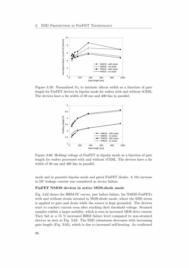
3. ESD Protection in FinFET Technology
0
2
4
6
8
10
0 200 400 600 800 1000
NMOS - with strainNMOS - no strainPMOS - with strainPMOS - no strain
Nor
mal
ized
failu
re c
urre
nt It
2 [m
A/u
m]
Gate length [nm]
Figure 3.59: Normalized It2 to intrinsic silicon width as a function of gatelength for FinFET devices in bipolar mode for wafers with and without tCESL.The devices have a fin width of 30 nm and 400 fins in parallel.
2
2.5
3
3.5
4
4.5
5
0 200 400 600 800 1000
NMOS - with strainNMOS - no strainPMOS - with strainPMOS - no strain
Hol
ding
vol
tage
[V]
Gate length [nm]
Figure 3.60: Holding voltage of FinFET in bipolar mode as a function of gatelength for wafers processed with and without tCESL. The devices have a finwidth of 30 nm and 400 fins in parallel.
mode and in parasitic-bipolar mode and gated FinFET diodes. A 10x increasein DC leakage current was considered as device failure.
FinFET NMOS devices in active MOS-diode mode
Fig. 3.62 shows the HBM-IV curves, just before failure, for NMOS FinFETswith and without strain stressed in MOS-diode mode, where the ESD stressis applied to gate and drain while the source is kept grounded. The devicesstart to conduct current soon after reaching their threshold voltage. Strainedsamples exhibit a larger mobility, which is seen in increased MOS drive current.They fail at a 15 % increased HBM failure level compared to non-straineddevices as seen in Fig. 3.63. The ESD robustness decreases with increasinggate length (Fig. 3.63), which is due to increased self-heating. As confirmed
98
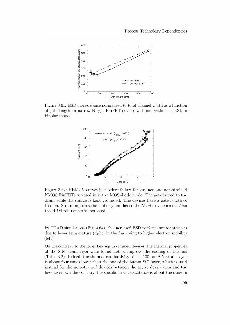
Process Technology Dependencies
0
100
200
300
400
500
600
0 200 400 600 800 1000
with strainwithout strain
Nor
mal
ized
on-
resi
stan
ce [O
hm u
m]
Gate length [nm]
Figure 3.61: ESD on-resistance normalized to total channel width as a functionof gate length for narrow N-type FinFET devices with and without tCESL inbipolar mode.
0
20
40
60
80
100
0 1 2 3 4
no strain (VHBM
=140 V)
strain (VHBM
=160 V)
Cur
rent
[mA
]
Voltage [V]
Figure 3.62: HBM-IV curves just before failure for strained and non-strainedNMOS FinFETs stressed in active MOS-diode mode. The gate is tied to thedrain while the source is kept grounded. The devices have a gate length of155 nm. Strain improves the mobility and hence the MOS-drive current. Alsothe HBM robustness is increased.
by TCAD simulations (Fig. 3.64), the increased ESD performance for strain isdue to lower temperature (right) in the fins owing to higher electron mobility(left).
On the contrary to the lower heating in strained devices, the thermal propertiesof the SiN strain layer were found not to improve the cooling of the fins(Table 3.2). Indeed, the thermal conductivity of the 100-nm SiN strain layeris about four times lower than the one of the 50-nm SiC layer, which is usedinstead for the non-strained devices between the active device area and thelow- layer. On the contrary, the specific heat capacitance is about the same in
99
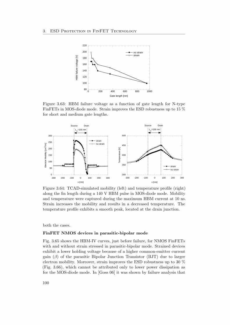
3. ESD Protection in FinFET Technology
80
100
120
140
160
180
200
220
0 200 400 600 800 1000
no strainstrain
HB
M fa
ilure
vol
tage
[V]
Gate length [nm]
Figure 3.63: HBM failure voltage as a function of gate length for N-typeFinFETs in MOS-diode mode. Strain improves the ESD robustness up to 15 %for short and medium gate lengths.
0
50
100
150
200
250
300
strainno strain
-300 -200 -100 0 100 200 300
Ele
ctro
n M
obili
ty [c
m2 /V
s]
LG=155 nm
Source Drain
x [nm]
300
350
400
450
500
strain
no strain
-300 -200 -100 0 100 200 300
Tem
pera
ture
[K]
x [nm]
LG=155 nm
Source Drain
Figure 3.64: TCAD-simulated mobility (left) and temperature profile (right)along the fin length during a 140 V HBM pulse in MOS-diode mode. Mobilityand temperature were captured during the maximum HBM current at 10 ns.Strain increases the mobility and results in a decreased temperature. Thetemperature profile exhibits a smooth peak, located at the drain junction.
both the cases.
FinFET NMOS devices in parasitic-bipolar mode
Fig. 3.65 shows the HBM-IV curves, just before failure, for NMOS FinFETswith and without strain stressed in parasitic-bipolar mode. Strained devicesexhibit a lower holding voltage because of a higher common-emitter currentgain (β) of the parasitic Bipolar Junction Transistor (BJT) due to largerelectron mobility. Moreover, strain improves the ESD robustness up to 30 %(Fig. 3.66), which cannot be attributed only to lower power dissipation asfor the MOS-diode mode. In [Goss 06] it was shown by failure analysis that
100
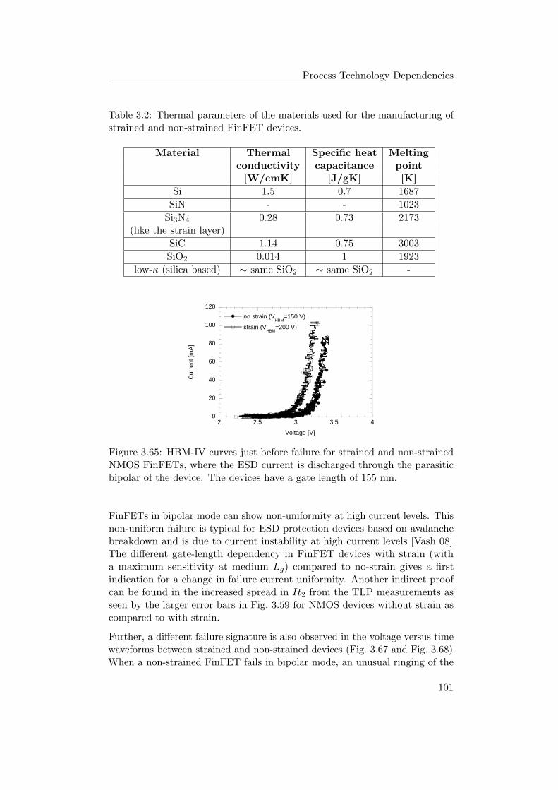
Process Technology Dependencies
Table 3.2: Thermal parameters of the materials used for the manufacturing ofstrained and non-strained FinFET devices.
Material Thermal Specific heat Meltingconductivity capacitance point[W/cmK] [J/gK] [K]
Si 1.5 0.7 1687SiN - - 1023
Si3N4 0.28 0.73 2173(like the strain layer)
SiC 1.14 0.75 3003SiO2 0.014 1 1923
low-κ (silica based) ∼ same SiO2 ∼ same SiO2 -
0
20
40
60
80
100
120
2 2.5 3 3.5 4
no strain (VHBM
=150 V)
strain (VHBM
=200 V)
Cur
rent
[mA
]
Voltage [V]
Figure 3.65: HBM-IV curves just before failure for strained and non-strainedNMOS FinFETs, where the ESD current is discharged through the parasiticbipolar of the device. The devices have a gate length of 155 nm.
FinFETs in bipolar mode can show non-uniformity at high current levels. Thisnon-uniform failure is typical for ESD protection devices based on avalanchebreakdown and is due to current instability at high current levels [Vash 08].The different gate-length dependency in FinFET devices with strain (witha maximum sensitivity at medium Lg) compared to no-strain gives a firstindication for a change in failure current uniformity. Another indirect proofcan be found in the increased spread in It2 from the TLP measurements asseen by the larger error bars in Fig. 3.59 for NMOS devices without strain ascompared to with strain.
Further, a different failure signature is also observed in the voltage versus timewaveforms between strained and non-strained devices (Fig. 3.67 and Fig. 3.68).When a non-strained FinFET fails in bipolar mode, an unusual ringing of the
101
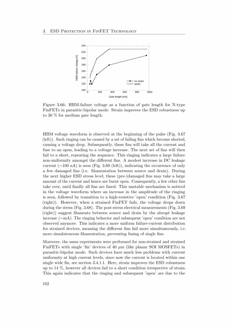
3. ESD Protection in FinFET Technology
100
120
140
160
180
200
220
240
0 200 400 600 800 1000
no strainstrain
HB
M fa
ilure
vol
tage
[V]
Gate length [nm]
Figure 3.66: HBM-failure voltage as a function of gate length for N-typeFinFETs in parasitic-bipolar mode. Strain improves the ESD robustness upto 30 % for medium gate length.
HBM voltage waveform is observed at the beginning of the pulse (Fig. 3.67(left)). Such ringing can be caused by a set of failing fins which become shorted,causing a voltage drop. Subsequently, these fins will take all the current andfuse to an open, leading to a voltage increase. The next set of fins will thenfail to a short, repeating the sequence. This ringing indicates a large failurenon-uniformity amongst the different fins. A modest increase in DC leakagecurrent (∼100 nA) is seen (Fig. 3.69 (left)), indicating the occurrence of onlya few damaged fins (i.e. filamentation between source and drain). Duringthe next higher ESD stress level, these (pre-)damaged fins may take a largeamount of the current and hence are burnt open. Consequently, a few other finstake over, until finally all fins are fused. This unstable mechanism is noticedin the voltage waveform where an increase in the amplitude of the ringingis seen, followed by transition to a high-resistive ’open’ condition (Fig. 3.67(right)). However, when a strained FinFET fails, the voltage drops downduring the stress (Fig. 3.68). The post-stress electrical measurements (Fig. 3.69(right)) suggest filaments between source and drain by the abrupt leakageincrease (∼mA). The ringing behavior and subsequent ’open’ condition are notobserved anymore. This indicates a more uniform failure-current distributionfor strained devices, meaning the different fins fail more simultaneously, i.e.more simulateneous filamentation, preventing fusing of single fins.
Moreover, the same experiments were performed for non-strained and strainedFinFETs with single ’fin’ devices of 40 µm (like planar SOI MOSFETs) inparasitic-bipolar mode. Such devices have much less problems with currentuniformity at high current levels, since now the current is located within onesingle wide fin, see section 3.4.1.1. Here, strain improves the ESD robustnessup to 14 %, however all devices fail to a short condition irrespective of strain.This again indicates that the ringing and subsequent ’open’ are due to the
102
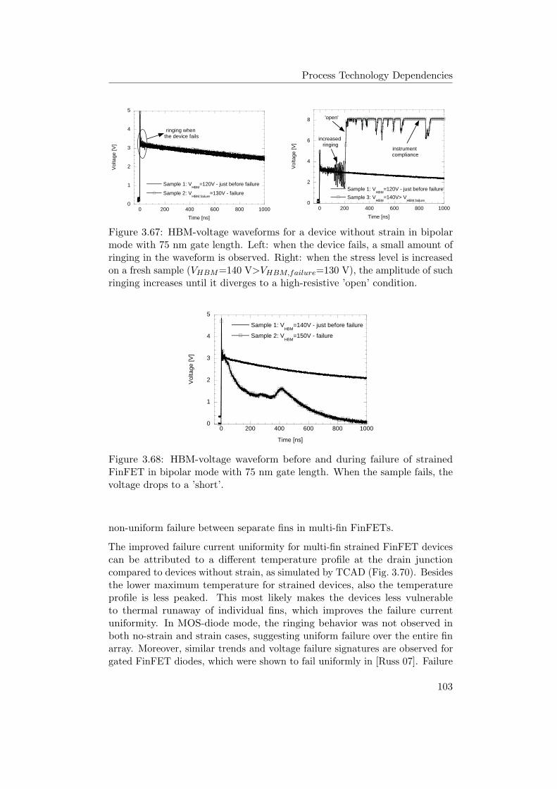
Process Technology Dependencies
0
1
2
3
4
5
0 200 400 600 800 1000
Sample 1: VHBM
=120V - just before failure
Sample 2: VHBM,failure
=130V - failure
Vol
tage
[V]
Time [ns]
ringing when the device fails
0
2
4
6
8
0 200 400 600 800 1000
Sample 1: VHBM
=120V - just before failure
Sample 3: VHBM
=140V> VHBM,failure
Vol
tage
[V]
Time [ns]
increased ringing
instrument compliance
'open'
Figure 3.67: HBM-voltage waveforms for a device without strain in bipolarmode with 75 nm gate length. Left: when the device fails, a small amount ofringing in the waveform is observed. Right: when the stress level is increasedon a fresh sample (VHBM=140 V>VHBM,failure=130 V), the amplitude of suchringing increases until it diverges to a high-resistive ’open’ condition.
0
1
2
3
4
5
0 200 400 600 800 1000
Sample 1: VHBM
=140V - just before failure
Sample 2: VHBM
=150V - failure
Vol
tage
[V]
Time [ns]
Figure 3.68: HBM-voltage waveform before and during failure of strainedFinFET in bipolar mode with 75 nm gate length. When the sample fails, thevoltage drops to a ’short’.
non-uniform failure between separate fins in multi-fin FinFETs.
The improved failure current uniformity for multi-fin strained FinFET devicescan be attributed to a different temperature profile at the drain junctioncompared to devices without strain, as simulated by TCAD (Fig. 3.70). Besidesthe lower maximum temperature for strained devices, also the temperatureprofile is less peaked. This most likely makes the devices less vulnerableto thermal runaway of individual fins, which improves the failure currentuniformity. In MOS-diode mode, the ringing behavior was not observed inboth no-strain and strain cases, suggesting uniform failure over the entire finarray. Moreover, similar trends and voltage failure signatures are observed forgated FinFET diodes, which were shown to fail uniformly in [Russ 07]. Failure
103
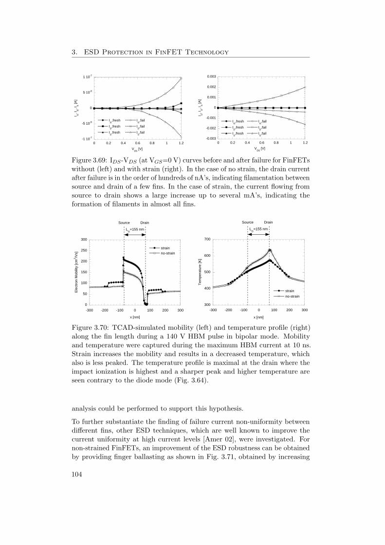
3. ESD Protection in FinFET Technology
-1 10-7
-5 10-8
0
5 10-8
1 10-7
IG,fresh
ID,fresh
IS,fresh
IG,fail
ID,fail
IS,fail
0 0.2 0.4 0.6 0.8 1 1.2
I G, I
D, I
S [A
]
VDS
[V]
-0.003
-0.002
-0.001
0
0.001
0.002
0.003
0 0.2 0.4 0.6 0.8 1 1.2
IG,fresh
ID,fresh
IS,fresh
IG,fail
ID,fail
IS,fail
I D, I
D, I
S [A
]
VDS
[V]
Figure 3.69: IDS-VDS (at VGS=0 V) curves before and after failure for FinFETswithout (left) and with strain (right). In the case of no strain, the drain currentafter failure is in the order of hundreds of nA’s, indicating filamentation betweensource and drain of a few fins. In the case of strain, the current flowing fromsource to drain shows a large increase up to several mA’s, indicating theformation of filaments in almost all fins.
0
50
100
150
200
250
300
strainno-strain
-300 -200 -100 0 100 200 300
Ele
ctro
n M
obili
ty [c
m2 /V
s]
LG=155 nm
Source Drain
x [nm]
300
400
500
600
700
strain
no-strain
-300 -200 -100 0 100 200 300
Tem
pera
ture
[K]
x [nm]
LG=155 nm
Source Drain
Figure 3.70: TCAD-simulated mobility (left) and temperature profile (right)along the fin length during a 140 V HBM pulse in bipolar mode. Mobilityand temperature were captured during the maximum HBM current at 10 ns.Strain increases the mobility and results in a decreased temperature, whichalso is less peaked. The temperature profile is maximal at the drain where theimpact ionization is highest and a sharper peak and higher temperature areseen contrary to the diode mode (Fig. 3.64).
analysis could be performed to support this hypothesis.
To further substantiate the finding of failure current non-uniformity betweendifferent fins, other ESD techniques, which are well known to improve thecurrent uniformity at high current levels [Amer 02], were investigated. Fornon-strained FinFETs, an improvement of the ESD robustness can be obtainedby providing finger ballasting as shown in Fig. 3.71, obtained by increasing
104
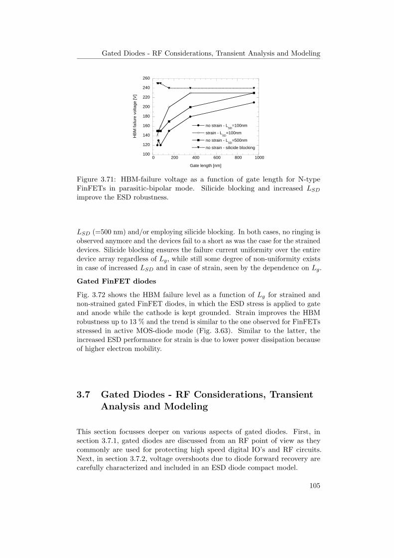
Gated Diodes - RF Considerations, Transient Analysis and Modeling
100
120
140
160
180
200
220
240
260
0 200 400 600 800 1000
no strain - LSD
=100nm
strain - LSD
=100nm
no strain - LSD
=500nm
no strain - silicide blocking
HB
M fa
ilure
vol
tage
[V]
Gate length [nm]
Figure 3.71: HBM-failure voltage as a function of gate length for N-typeFinFETs in parasitic-bipolar mode. Silicide blocking and increased LSD
improve the ESD robustness.
LSD (=500 nm) and/or employing silicide blocking. In both cases, no ringing isobserved anymore and the devices fail to a short as was the case for the straineddevices. Silicide blocking ensures the failure current uniformity over the entiredevice array regardless of Lg, while still some degree of non-uniformity existsin case of increased LSD and in case of strain, seen by the dependence on Lg.
Gated FinFET diodes
Fig. 3.72 shows the HBM failure level as a function of Lg for strained andnon-strained gated FinFET diodes, in which the ESD stress is applied to gateand anode while the cathode is kept grounded. Strain improves the HBMrobustness up to 13 % and the trend is similar to the one observed for FinFETsstressed in active MOS-diode mode (Fig. 3.63). Similar to the latter, theincreased ESD performance for strain is due to lower power dissipation becauseof higher electron mobility.
3.7 Gated Diodes - RF Considerations, TransientAnalysis and Modeling
This section focusses deeper on various aspects of gated diodes. First, insection 3.7.1, gated diodes are discussed from an RF point of view as theycommonly are used for protecting high speed digital IO’s and RF circuits.Next, in section 3.7.2, voltage overshoots due to diode forward recovery arecarefully characterized and included in an ESD diode compact model.
105
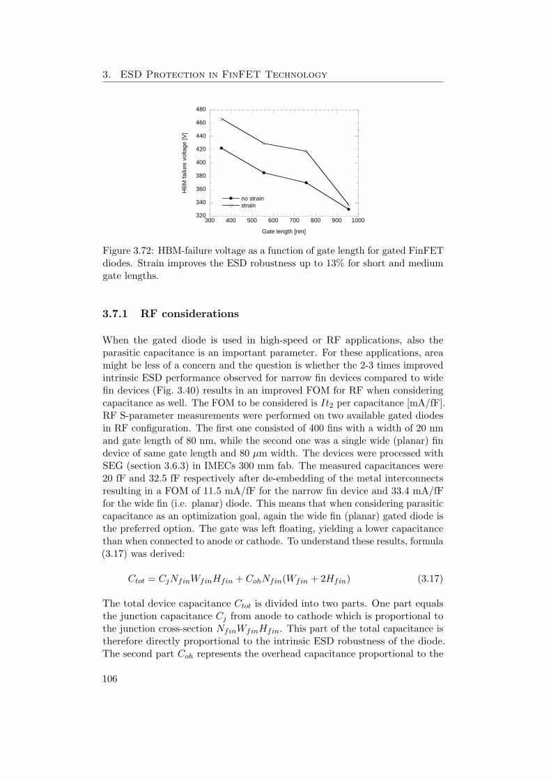
3. ESD Protection in FinFET Technology
320
340
360
380
400
420
440
460
480
300 400 500 600 700 800 900 1000
no strainstrain
HB
M fa
ilure
vol
tage
[V]
Gate length [nm]
Figure 3.72: HBM-failure voltage as a function of gate length for gated FinFETdiodes. Strain improves the ESD robustness up to 13% for short and mediumgate lengths.
3.7.1 RF considerations
When the gated diode is used in high-speed or RF applications, also theparasitic capacitance is an important parameter. For these applications, areamight be less of a concern and the question is whether the 2-3 times improvedintrinsic ESD performance observed for narrow fin devices compared to widefin devices (Fig. 3.40) results in an improved FOM for RF when consideringcapacitance as well. The FOM to be considered is It2 per capacitance [mA/fF].RF S-parameter measurements were performed on two available gated diodesin RF configuration. The first one consisted of 400 fins with a width of 20 nmand gate length of 80 nm, while the second one was a single wide (planar) findevice of same gate length and 80 µm width. The devices were processed withSEG (section 3.6.3) in IMECs 300 mm fab. The measured capacitances were20 fF and 32.5 fF respectively after de-embedding of the metal interconnectsresulting in a FOM of 11.5 mA/fF for the narrow fin device and 33.4 mA/fFfor the wide fin (i.e. planar) diode. This means that when considering parasiticcapacitance as an optimization goal, again the wide fin (planar) gated diode isthe preferred option. The gate was left floating, yielding a lower capacitancethan when connected to anode or cathode. To understand these results, formula(3.17) was derived:
Ctot = CjNfinWfinHfin + CohNfin(Wfin + 2Hfin) (3.17)
The total device capacitance Ctot is divided into two parts. One part equalsthe junction capacitance Cj from anode to cathode which is proportional tothe junction cross-section NfinWfinHfin. This part of the total capacitance istherefore directly proportional to the intrinsic ESD robustness of the diode.The second part Coh represents the overhead capacitance proportional to the
106
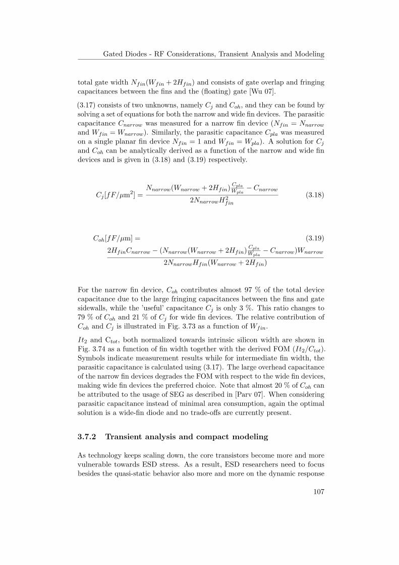
Gated Diodes - RF Considerations, Transient Analysis and Modeling
total gate width Nfin(Wfin + 2Hfin) and consists of gate overlap and fringingcapacitances between the fins and the (floating) gate [Wu 07].
(3.17) consists of two unknowns, namely Cj and Coh, and they can be found bysolving a set of equations for both the narrow and wide fin devices. The parasiticcapacitance Cnarrow was measured for a narrow fin device (Nfin = Nnarrow
and Wfin = Wnarrow). Similarly, the parasitic capacitance Cpla was measuredon a single planar fin device Nfin = 1 and Wfin = Wpla). A solution for Cj
and Coh can be analytically derived as a function of the narrow and wide findevices and is given in (3.18) and (3.19) respectively.
Cj [fF/µm2] =Nnarrow(Wnarrow + 2Hfin) Cpla
Wpla− Cnarrow
2NnarrowH2fin
(3.18)
Coh[fF/µm] = (3.19)
2HfinCnarrow − (Nnarrow(Wnarrow + 2Hfin) Cpla
Wpla− Cnarrow)Wnarrow
2NnarrowHfin(Wnarrow + 2Hfin)
For the narrow fin device, Coh contributes almost 97 % of the total devicecapacitance due to the large fringing capacitances between the fins and gatesidewalls, while the ’useful’ capacitance Cj is only 3 %. This ratio changes to79 % of Coh and 21 % of Cj for wide fin devices. The relative contribution ofCoh and Cj is illustrated in Fig. 3.73 as a function of Wfin.
It2 and Ctot, both normalized towards intrinsic silicon width are shown inFig. 3.74 as a function of fin width together with the derived FOM (It2/Ctot).Symbols indicate measurement results while for intermediate fin width, theparasitic capacitance is calculated using (3.17). The large overhead capacitanceof the narrow fin devices degrades the FOM with respect to the wide fin devices,making wide fin devices the preferred choice. Note that almost 20 % of Coh canbe attributed to the usage of SEG as described in [Parv 07]. When consideringparasitic capacitance instead of minimal area consumption, again the optimalsolution is a wide-fin diode and no trade-offs are currently present.
3.7.2 Transient analysis and compact modeling
As technology keeps scaling down, the core transistors become more and morevulnerable towards ESD stress. As a result, ESD researchers need to focusbesides the quasi-static behavior also more and more on the dynamic response
107
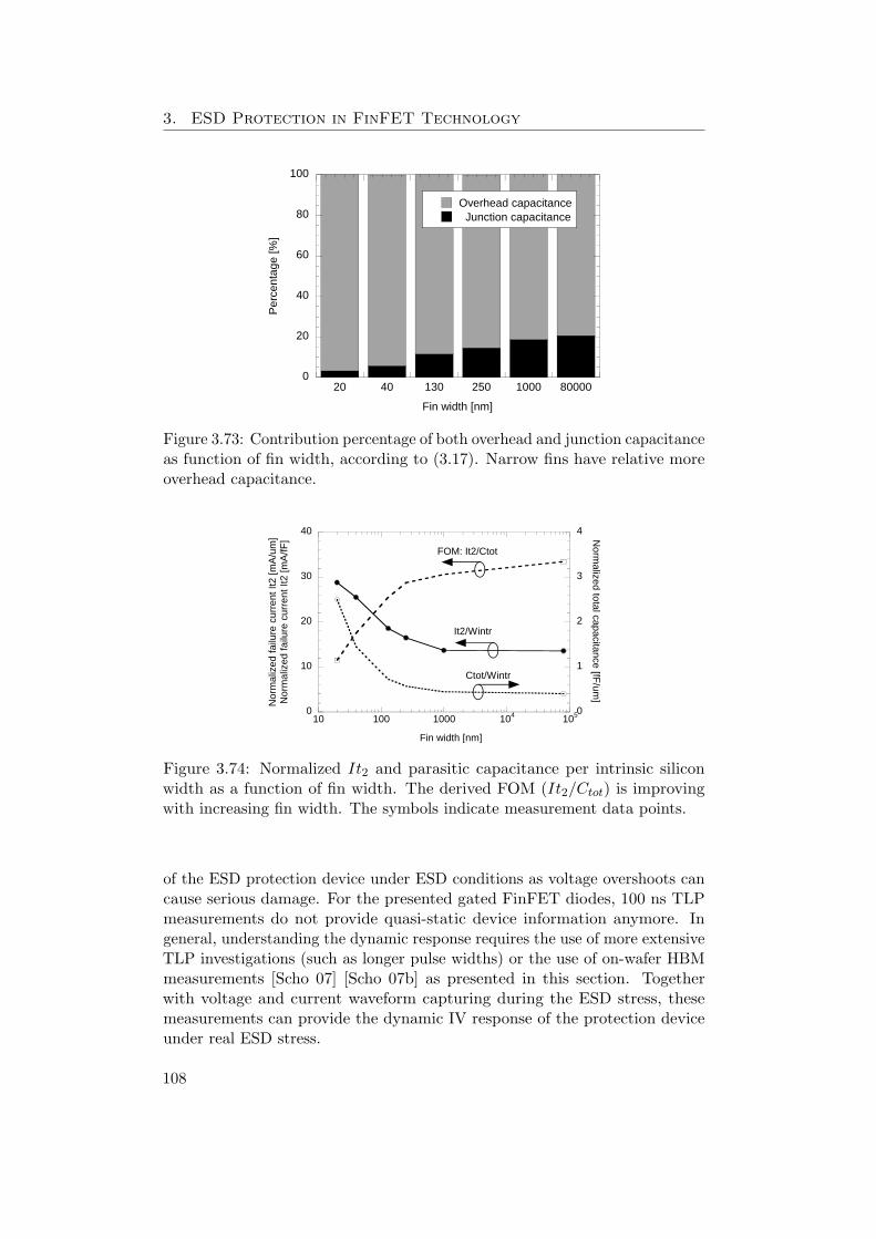
3. ESD Protection in FinFET Technology
0
20
40
60
80
100
20 40 130 250 1000 80000
Junction capacitance
Per
cent
age
[%]
Fin width [nm]
Overhead capacitance
Figure 3.73: Contribution percentage of both overhead and junction capacitanceas function of fin width, according to (3.17). Narrow fins have relative moreoverhead capacitance.
0
10
20
30
40
0
1
2
3
4
10 100 1000 104 105
Nor
mal
ized
failu
re c
urre
nt It
2 [m
A/u
m]
Nor
mal
ized
failu
re c
urre
nt It
2 [m
A/fF
] Norm
alized total capacitance [fF/um
]
Fin width [nm]
It2/Wintr
FOM: It2/Ctot
Ctot/Wintr
Figure 3.74: Normalized It2 and parasitic capacitance per intrinsic siliconwidth as a function of fin width. The derived FOM (It2/Ctot) is improvingwith increasing fin width. The symbols indicate measurement data points.
of the ESD protection device under ESD conditions as voltage overshoots cancause serious damage. For the presented gated FinFET diodes, 100 ns TLPmeasurements do not provide quasi-static device information anymore. Ingeneral, understanding the dynamic response requires the use of more extensiveTLP investigations (such as longer pulse widths) or the use of on-wafer HBMmeasurements [Scho 07] [Scho 07b] as presented in this section. Togetherwith voltage and current waveform capturing during the ESD stress, thesemeasurements can provide the dynamic IV response of the protection deviceunder real ESD stress.
108
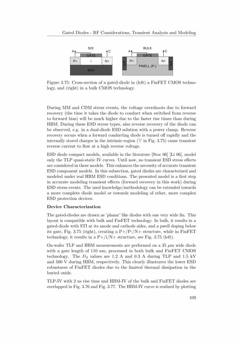
Gated Diodes - RF Considerations, Transient Analysis and Modeling
PWELL (P-)
i
GATE
N+P+
SOIA C
BOX
GATE
N+P+
BULKA C
ST
I
ST
I
Figure 3.75: Cross-section of a gated-diode in (left) a FinFET CMOS techno-logy, and (right) in a bulk CMOS technology.
During MM and CDM stress events, the voltage overshoots due to forwardrecovery (the time it takes the diode to conduct when switched from reverseto forward bias) will be much higher due to the faster rise times than duringHBM. During these ESD stress types, also reverse recovery of the diode canbe observed, e.g. in a dual-diode ESD solution with a power clamp. Reverserecovery occurs when a forward conducting diode is turned off rapidly and theinternally stored charges in the intrinsic-region (’i’ in Fig. 3.75) cause transientreverse current to flow at a high reverse voltage.
ESD diode compact models, available in the literature [Stoc 06] [Li 06], modelonly the TLP quasi-static IV curves. Until now, no transient ESD stress effectsare considered in these models. This enhances the necessity of accurate transientESD component models. In this subsection, gated diodes are characterized andmodeled under real HBM ESD conditions. The presented model is a first stepin accurate modeling transient effects (forward recovery in this work) duringESD stress events. The used knowledge/methodology can be extended towardsa more complete diode model or towards modeling of other, more complexESD protection devices.
Device Characterization
The gated-diodes are drawn as ’planar’ like diodes with one very wide fin. Thislayout is compatible with bulk and FinFET technology. In bulk, it results in agated-diode with STI at its anode and cathode sides, and a pwell doping belowits gate, Fig. 3.75 (right), creating a P+/P-/N+ structure, while in FinFETtechnology, it results in a P+/i/N+ structure, see Fig. 3.75 (left).
On-wafer TLP and HBM measurements are performed on a 35 µm wide diodewith a gate length of 110 nm, processed in both bulk and FinFET CMOStechnology. The It2 values are 1.2 A and 0.3 A during TLP and 1.5 kVand 500 V during HBM, respectively. This clearly illustrates the lower ESDrobustness of FinFET diodes due to the limited thermal dissipation in theburied oxide.
TLP-IV with 2 ns rise time and HBM-IV of the bulk and FinFET diodes areoverlapped in Fig. 3.76 and Fig. 3.77. The HBM-IV curve is realized by plotting
109
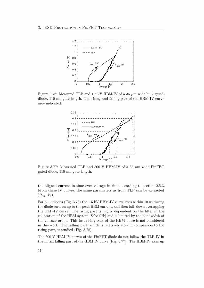
3. ESD Protection in FinFET Technology
0
0.2
0.4
0.6
0.8
1
1.2
1.4
0 0.5 1 1.5 2 2.5
1.5 kV HBM
TLP
Cur
rent
[A]
Voltage [V]
tHBM
risetHBM
fall
Figure 3.76: Measured TLP and 1.5 kV HBM-IV of a 35 µm wide bulk gated-diode, 110 nm gate length. The rising and falling part of the HBM-IV curvearee indicated.
0
0.05
0.1
0.15
0.2
0.25
0.3
0.35
0.6 0.8 1 1.2 1.4
500V HBM IV
TLP
Cur
rent
[A]
Voltage [V]
A
BB
C
tHBM
rise
tHBM
fall
Figure 3.77: Measured TLP and 500 V HBM-IV of a 35 µm wide FinFETgated-diode, 110 nm gate length.
the aligned current in time over voltage in time according to section 2.5.3.From these IV curves, the same parameters as from TLP can be extracted(Ron, Vh).
For bulk diodes (Fig. 3.76) the 1.5 kV HBM-IV curve rises within 10 ns duringthe diode turn-on up to the peak HBM current, and then falls down overlappingthe TLP-IV curve. The rising part is highly dependent on the filter in thecalibration of the HBM system [Scho 07b] and is limited by the bandwidth ofthe voltage probe. This fast rising part of the HBM pulse is not consideredin this work. The falling part, which is relatively slow in comparison to therising part, is studied (Fig. 3.78).
The 500 V HBM-IV curves of the FinFET diode do not follow the TLP-IV inthe initial falling part of the HBM IV curve (Fig. 3.77). The HBM-IV rises up
110
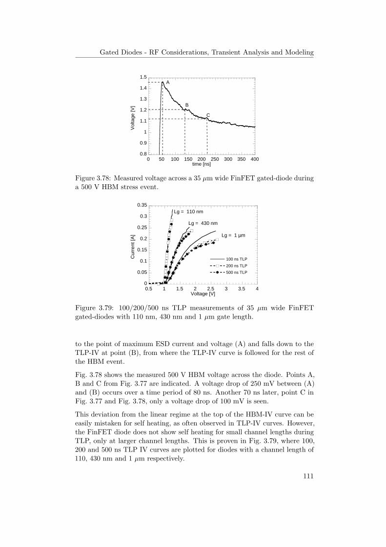
Gated Diodes - RF Considerations, Transient Analysis and Modeling
0.8
0.9
1
1.1
1.2
1.3
1.4
1.5
0 50 100 150 200 250 300 350 400
Vol
tage
[V]
time [ns]
A
B
C
Figure 3.78: Measured voltage across a 35 µm wide FinFET gated-diode duringa 500 V HBM stress event.
0
0.05
0.1
0.15
0.2
0.25
0.3
0.35
0.5 1 1.5 2 2.5 3 3.5 4
100 ns TLP
200 ns TLP
500 ns TLP
Cur
rent
[A]
Voltage [V]
Lg = 110 nm
Lg = 430 nm
Lg = 1 µm
Figure 3.79: 100/200/500 ns TLP measurements of 35 µm wide FinFETgated-diodes with 110 nm, 430 nm and 1 µm gate length.
to the point of maximum ESD current and voltage (A) and falls down to theTLP-IV at point (B), from where the TLP-IV curve is followed for the rest ofthe HBM event.
Fig. 3.78 shows the measured 500 V HBM voltage across the diode. Points A,B and C from Fig. 3.77 are indicated. A voltage drop of 250 mV between (A)and (B) occurs over a time period of 80 ns. Another 70 ns later, point C inFig. 3.77 and Fig. 3.78, only a voltage drop of 100 mV is seen.
This deviation from the linear regime at the top of the HBM-IV curve can beeasily mistaken for self heating, as often observed in TLP-IV curves. However,the FinFET diode does not show self heating for small channel lengths duringTLP, only at larger channel lengths. This is proven in Fig. 3.79, where 100,200 and 500 ns TLP IV curves are plotted for diodes with a channel length of110, 430 nm and 1 µm respectively.
111
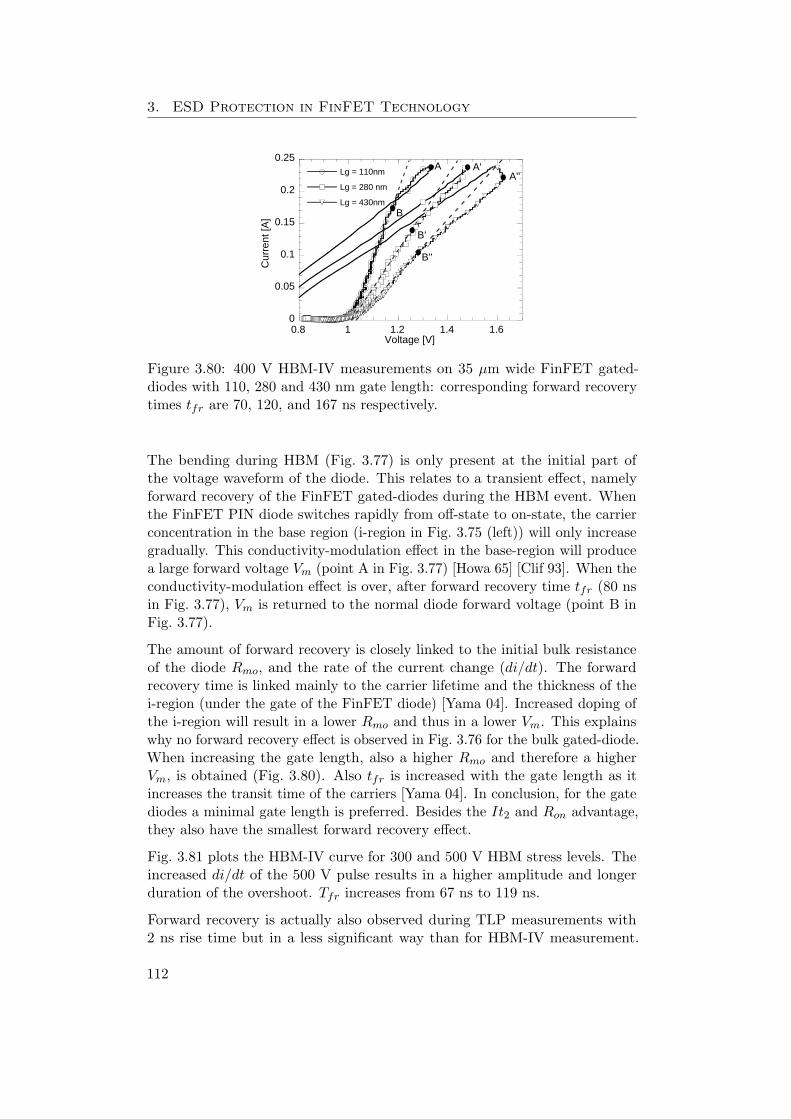
3. ESD Protection in FinFET Technology
0
0.05
0.1
0.15
0.2
0.25
0.8 1 1.2 1.4 1.6
Lg = 110nm
Lg = 280 nm
Lg = 430nm
Cur
rent
[A]
Voltage [V]
A
B
A'
B'
A''
B''
Figure 3.80: 400 V HBM-IV measurements on 35 µm wide FinFET gated-diodes with 110, 280 and 430 nm gate length: corresponding forward recoverytimes tfr are 70, 120, and 167 ns respectively.
The bending during HBM (Fig. 3.77) is only present at the initial part ofthe voltage waveform of the diode. This relates to a transient effect, namelyforward recovery of the FinFET gated-diodes during the HBM event. Whenthe FinFET PIN diode switches rapidly from off-state to on-state, the carrierconcentration in the base region (i-region in Fig. 3.75 (left)) will only increasegradually. This conductivity-modulation effect in the base-region will producea large forward voltage Vm (point A in Fig. 3.77) [Howa 65] [Clif 93]. When theconductivity-modulation effect is over, after forward recovery time tfr (80 nsin Fig. 3.77), Vm is returned to the normal diode forward voltage (point B inFig. 3.77).
The amount of forward recovery is closely linked to the initial bulk resistanceof the diode Rmo, and the rate of the current change (di/dt). The forwardrecovery time is linked mainly to the carrier lifetime and the thickness of thei-region (under the gate of the FinFET diode) [Yama 04]. Increased doping ofthe i-region will result in a lower Rmo and thus in a lower Vm. This explainswhy no forward recovery effect is observed in Fig. 3.76 for the bulk gated-diode.When increasing the gate length, also a higher Rmo and therefore a higherVm, is obtained (Fig. 3.80). Also tfr is increased with the gate length as itincreases the transit time of the carriers [Yama 04]. In conclusion, for the gatediodes a minimal gate length is preferred. Besides the It2 and Ron advantage,they also have the smallest forward recovery effect.
Fig. 3.81 plots the HBM-IV curve for 300 and 500 V HBM stress levels. Theincreased di/dt of the 500 V pulse results in a higher amplitude and longerduration of the overshoot. Tfr increases from 67 ns to 119 ns.
Forward recovery is actually also observed during TLP measurements with2 ns rise time but in a less significant way than for HBM-IV measurement.
112
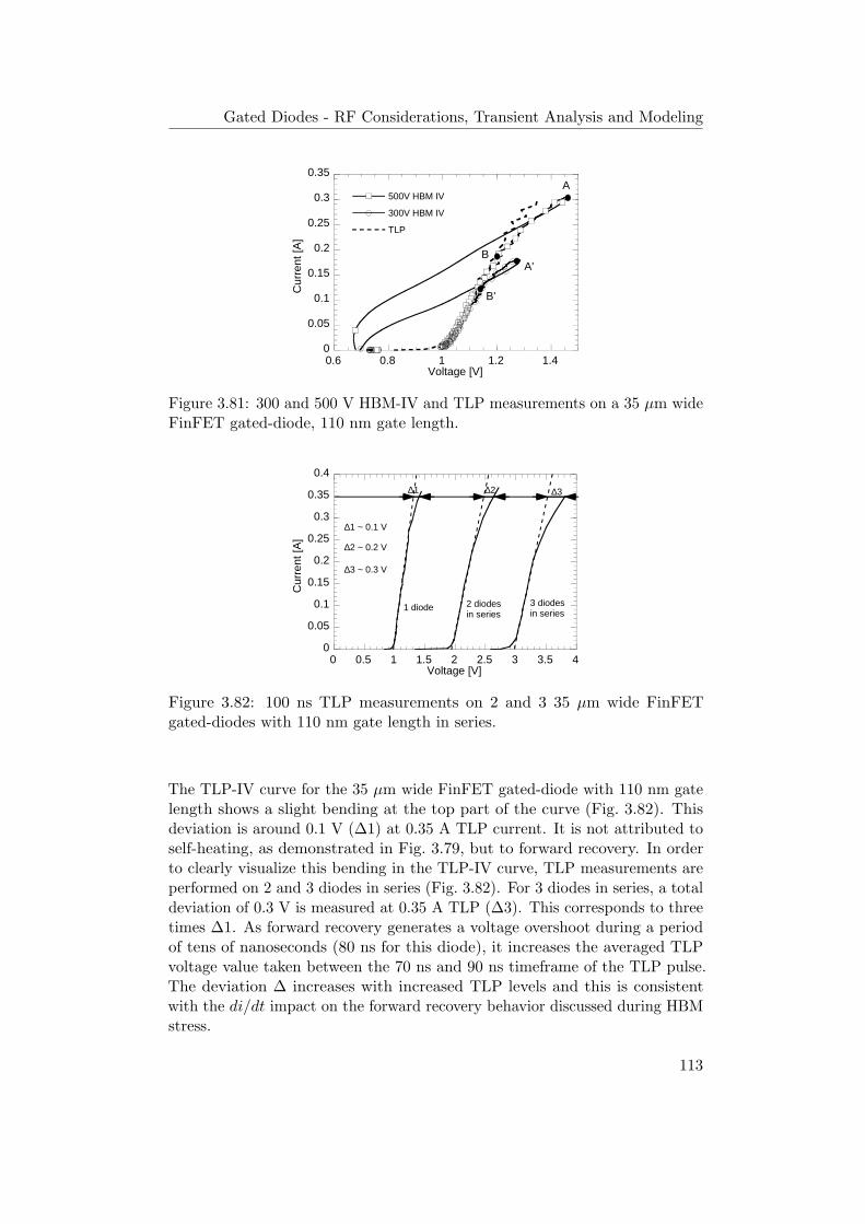
Gated Diodes - RF Considerations, Transient Analysis and Modeling
0
0.05
0.1
0.15
0.2
0.25
0.3
0.35
0.6 0.8 1 1.2 1.4
500V HBM IV
300V HBM IV
TLP
Cur
rent
[A]
Voltage [V]
A
BA'
B'
Figure 3.81: 300 and 500 V HBM-IV and TLP measurements on a 35 µm wideFinFET gated-diode, 110 nm gate length.
0
0.05
0.1
0.15
0.2
0.25
0.3
0.35
0.4
0 0.5 1 1.5 2 2.5 3 3.5 4
Cur
rent
[A]
Voltage [V]
3 diodesin series
2 diodesin series
1 diode
∆1 ∆2 ∆3
∆1 ~ 0.1 V
∆2 ~ 0.2 V
∆3 ~ 0.3 V
Figure 3.82: 100 ns TLP measurements on 2 and 3 35 µm wide FinFETgated-diodes with 110 nm gate length in series.
The TLP-IV curve for the 35 µm wide FinFET gated-diode with 110 nm gatelength shows a slight bending at the top part of the curve (Fig. 3.82). Thisdeviation is around 0.1 V (∆1) at 0.35 A TLP current. It is not attributed toself-heating, as demonstrated in Fig. 3.79, but to forward recovery. In orderto clearly visualize this bending in the TLP-IV curve, TLP measurements areperformed on 2 and 3 diodes in series (Fig. 3.82). For 3 diodes in series, a totaldeviation of 0.3 V is measured at 0.35 A TLP (∆3). This corresponds to threetimes ∆1. As forward recovery generates a voltage overshoot during a periodof tens of nanoseconds (80 ns for this diode), it increases the averaged TLPvoltage value taken between the 70 ns and 90 ns timeframe of the TLP pulse.The deviation ∆ increases with increased TLP levels and this is consistentwith the di/dt impact on the forward recovery behavior discussed during HBMstress.
113
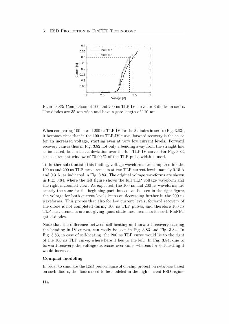
3. ESD Protection in FinFET Technology
0
0.05
0.1
0.15
0.2
0.25
0.3
0.35
0.4
2 2.5 3 3.5 4
100ns TLP
200ns TLP
Cur
rent
[A]
Voltage [V]
Figure 3.83: Comparison of 100 and 200 ns TLP-IV curve for 3 diodes in series.The diodes are 35 µm wide and have a gate length of 110 nm.
When comparing 100 ns and 200 ns TLP-IV for the 3 diodes in series (Fig. 3.83),it becomes clear that in the 100 ns TLP-IV curve, forward recovery is the causefor an increased voltage, starting even at very low current levels. Forwardrecovery causes thus in Fig. 3.82 not only a bending away from the straight lineas indicated, but in fact a deviation over the full TLP IV curve. For Fig. 3.83,a measurement window of 70-90 % of the TLP pulse width is used.
To further substantiate this finding, voltage waveforms are compared for the100 ns and 200 ns TLP measurements at two TLP current levels, namely 0.15 Aand 0.3 A, as indicated in Fig. 3.83. The original voltage waveforms are shownin Fig. 3.84, where the left figure shows the full TLP voltage waveform andthe right a zoomed view. As expected, the 100 ns and 200 ns waveforms areexactly the same for the beginning part, but as can be seen in the right figure,the voltage for both current levels keeps on decreasing further in the 200 nswaveforms. This proves that also for low current levels, forward recovery ofthe diode is not completed during 100 ns TLP pulses, and therefore 100 nsTLP measurements are not giving quasi-static measurements for such FinFETgated-diodes.
Note that the difference between self-heating and forward recovery causingthe bending in IV curves, can easily be seen in Fig. 3.83 and Fig. 3.84. InFig. 3.83, in case of self-heating, the 200 ns TLP curve would lie to the rightof the 100 ns TLP curve, where here it lies to the left. In Fig. 3.84, due toforward recovery the voltage decreases over time, whereas for self-heating itwould increase.
Compact modeling
In order to simulate the ESD performance of on-chip protection networks basedon such diodes, the diodes need to be modeled in the high current ESD regime
114
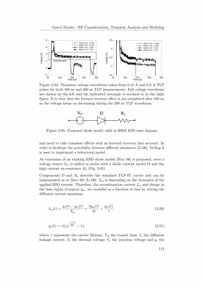
Gated Diodes - RF Considerations, Transient Analysis and Modeling
-2
0
2
4
6
8
50 100 150 200 250
100ns TLP - 0.15A200ns TLP - 0.15A100ns TLP - 0.3A200ns TLP - 0.3A
Vol
tage
[V]
Time [ns]
zoomed area
2.5
3
3.5
4
4.5
50 100 150 200 250
100ns TLP - 0.15A200ns TLP - 0.15A100ns TLP - 0.3A200ns TLP - 0.3A
Vol
tage
[V]
Time [ns]
Figure 3.84: Transient voltage waveforms taken from 0.15 A and 0.3 A TLPpulses for both 100 ns and 200 ns TLP measurements. Full voltage waveformsare shown on the left and the indicated rectangle is zoomed to in the rightfigure. It is clear that the forward recovery effect is not completed after 100 ns,as the voltage keeps on decreasing during the 200 ns TLP waveforms.
Figure 3.85: Proposed diode model valid in HBM ESD time domain.
and need to take transient effects such as forward recovery into account. Inorder to facilitate the portability between different simulators [Li 06], Verilog-Ais used to implement a behavioral model.
An extension of an existing ESD diode model [Stoc 06] is proposed, were avoltage source Vm is added in series with a diode current model D and thehigh current on-resistance Rs (Fig. 3.85).
Components D and Rs describe the standard TLP-IV curves and can beimplemented as in [Stoc 06] [Li 06]. Vm is depending on the dynamics of theapplied ESD current. Therefore, the recombination current Im and charge inthe base region (I-region) qm, are modeled as a function of time by solving thediffusion current equations:
Im(t) =qe(t)− qm(t)
Tm=
δqm(t)δt
+qm(t)
τ, (3.20)
qe(t) = τIs(eVj(t)
2Vt − 1), (3.21)
where τ represents the carrier lifetime, Tm the transit time, Is the diffusionleakage current, Vt the thermal voltage, Vj the junction voltage and qe the
115
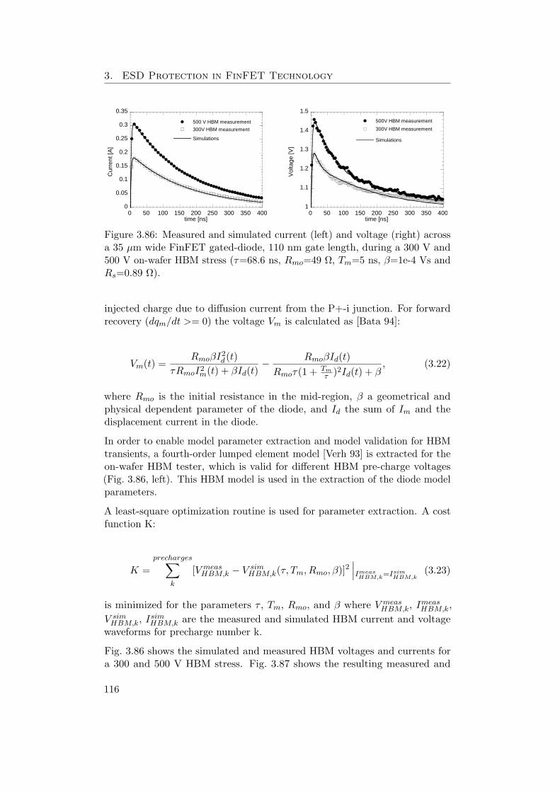
3. ESD Protection in FinFET Technology
0
0.05
0.1
0.15
0.2
0.25
0.3
0.35
0 50 100 150 200 250 300 350 400
Simulations
300V HBM measurement
500 V HBM measurement
Cur
rent
[A]
time [ns]
1
1.1
1.2
1.3
1.4
1.5
0 50 100 150 200 250 300 350 400
Simulations
300V HBM measurement
500V HBM measurement
Vol
tage
[V]
time [ns]
Figure 3.86: Measured and simulated current (left) and voltage (right) acrossa 35 µm wide FinFET gated-diode, 110 nm gate length, during a 300 V and500 V on-wafer HBM stress (τ=68.6 ns, Rmo=49 Ω, Tm=5 ns, β=1e-4 Vs andRs=0.89 Ω).
injected charge due to diffusion current from the P+-i junction. For forwardrecovery (dqm/dt >= 0) the voltage Vm is calculated as [Bata 94]:
Vm(t) =RmoβI2
d(t)τRmoI2
m(t) + βId(t)− RmoβId(t)
Rmoτ(1 + Tmτ )2Id(t) + β
, (3.22)
where Rmo is the initial resistance in the mid-region, β a geometrical andphysical dependent parameter of the diode, and Id the sum of Im and thedisplacement current in the diode.
In order to enable model parameter extraction and model validation for HBMtransients, a fourth-order lumped element model [Verh 93] is extracted for theon-wafer HBM tester, which is valid for different HBM pre-charge voltages(Fig. 3.86, left). This HBM model is used in the extraction of the diode modelparameters.
A least-square optimization routine is used for parameter extraction. A costfunction K:
K =precharges∑
k
[V measHBM,k − V sim
HBM,k(τ, Tm, Rmo, β)]2∣∣∣Imeas
HBM,k=IsimHBM,k
(3.23)
is minimized for the parameters τ , Tm, Rmo, and β where V measHBM,k, Imeas
HBM,k,V sim
HBM,k, IsimHBM,k are the measured and simulated HBM current and voltage
waveforms for precharge number k.
Fig. 3.86 shows the simulated and measured HBM voltages and currents fora 300 and 500 V HBM stress. Fig. 3.87 shows the resulting measured and
116
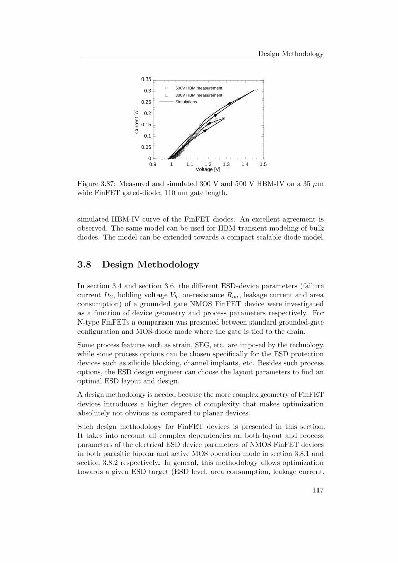
Design Methodology
0
0.05
0.1
0.15
0.2
0.25
0.3
0.35
0.9 1 1.1 1.2 1.3 1.4 1.5
Simulations
300V HBM measurement
500V HBM measurement
Cur
rent
[A]
Voltage [V]
Figure 3.87: Measured and simulated 300 V and 500 V HBM-IV on a 35 µmwide FinFET gated-diode, 110 nm gate length.
simulated HBM-IV curve of the FinFET diodes. An excellent agreement isobserved. The same model can be used for HBM transient modeling of bulkdiodes. The model can be extended towards a compact scalable diode model.
3.8 Design Methodology
In section 3.4 and section 3.6, the different ESD-device parameters (failurecurrent It2, holding voltage Vh, on-resistance Ron, leakage current and areaconsumption) of a grounded gate NMOS FinFET device were investigatedas a function of device geometry and process parameters respectively. ForN-type FinFETs a comparison was presented between standard grounded-gateconfiguration and MOS-diode mode where the gate is tied to the drain.
Some process features such as strain, SEG, etc. are imposed by the technology,while some process options can be chosen specifically for the ESD protectiondevices such as silicide blocking, channel implants, etc. Besides such processoptions, the ESD design engineer can choose the layout parameters to find anoptimal ESD layout and design.
A design methodology is needed because the more complex geometry of FinFETdevices introduces a higher degree of complexity that makes optimizationabsolutely not obvious as compared to planar devices.
Such design methodology for FinFET devices is presented in this section.It takes into account all complex dependencies on both layout and processparameters of the electrical ESD device parameters of NMOS FinFET devicesin both parasitic bipolar and active MOS operation mode in section 3.8.1 andsection 3.8.2 respectively. In general, this methodology allows optimizationtowards a given ESD target (ESD level, area consumption, leakage current,
117
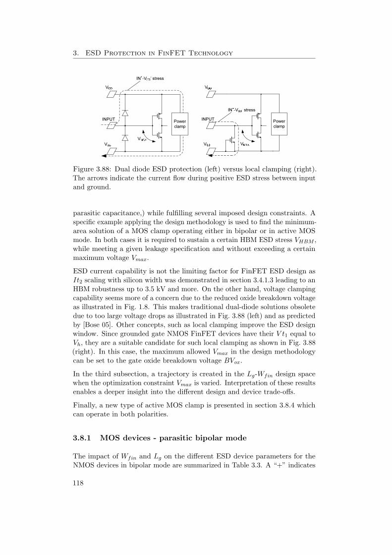
3. ESD Protection in FinFET Technology
INPUT
VDD
VSS
IN+-VSS- stress
Power clamp
VMAX INPUT
VDD
VSSIN+-VSS- stress
Power clamp
VMAXFigure 3.88: Dual diode ESD protection (left) versus local clamping (right).The arrows indicate the current flow during positive ESD stress between inputand ground.
parasitic capacitance,) while fulfilling several imposed design constraints. Aspecific example applying the design methodology is used to find the minimum-area solution of a MOS clamp operating either in bipolar or in active MOSmode. In both cases it is required to sustain a certain HBM ESD stress VHBM ,while meeting a given leakage specification and without exceeding a certainmaximum voltage Vmax.
ESD current capability is not the limiting factor for FinFET ESD design asIt2 scaling with silicon width was demonstrated in section 3.4.1.3 leading to anHBM robustness up to 3.5 kV and more. On the other hand, voltage clampingcapability seems more of a concern due to the reduced oxide breakdown voltageas illustrated in Fig. 1.8. This makes traditional dual-diode solutions obsoletedue to too large voltage drops as illustrated in Fig. 3.88 (left) and as predictedby [Bose 05]. Other concepts, such as local clamping improve the ESD designwindow. Since grounded gate NMOS FinFET devices have their V t1 equal toVh, they are a suitable candidate for such local clamping as shown in Fig. 3.88(right). In this case, the maximum allowed Vmax in the design methodologycan be set to the gate oxide breakdown voltage BVox .
In the third subsection, a trajectory is created in the Lg-Wfin design spacewhen the optimization constraint Vmax is varied. Interpretation of these resultsenables a deeper insight into the different design and device trade-offs.
Finally, a new type of active MOS clamp is presented in section 3.8.4 whichcan operate in both polarities.
3.8.1 MOS devices - parasitic bipolar mode
The impact of Wfin and Lg on the different ESD device parameters for theNMOS devices in bipolar mode are summarized in Table 3.3. A “+” indicates
118
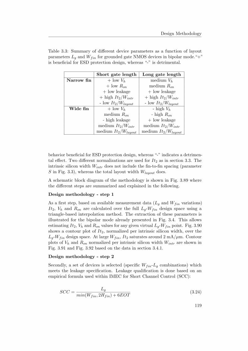
Design Methodology
Table 3.3: Summary of different device parameters as a function of layoutparameters Lg and Wfin for grounded gate NMOS devices in bipolar mode.“+”is beneficial for ESD protection design, whereas “-” is detrimental.
Short gate length Long gate lengthNarrow fin + low Vh medium Vh
+ low Ron medium Ron
+ low leakage + low leakage+ high It2/Wintr + high It2/Wintr
- low It2/Wlayout - low It2/Wlayout
Wide fin + low Vh - high Vh
medium Ron - high Ron
- high leakage + low leakagemedium It2/Wintr medium It2/Wintr
medium It2/Wlayout medium It2/Wlayout
behavior beneficial for ESD protection design, whereas “-” indicates a detrimen-tal effect. Two different normalizations are used for It2 as in section 3.3. Theintrinsic silicon width Wintr does not include the fin-to-fin spacing (parameterS in Fig. 3.3), whereas the total layout width Wlayout does.
A schematic block diagram of the methodology is shown in Fig. 3.89 wherethe different steps are summarized and explained in the following.
Design methodology - step 1
As a first step, based on available measurement data (Lg and Wfin variations)It2, Vh and Ron are calculated over the full Lg-Wfin design space using atriangle-based interpolation method. The extraction of these parameters isillustrated for the bipolar mode already presented in Fig. 3.4. This allowsestimating It2, Vh and Ron values for any given virtual Lg-Wfin point. Fig. 3.90shows a contour plot of It2, normalized per intrinsic silicon width, over theLg-Wfin design space. At large Wfin, It2 saturates around 2 mA/µm. Contourplots of Vh and Ron normalized per intrinsic silicon width Wintr are shown inFig. 3.91 and Fig. 3.92 based on the data in section 3.4.1.
Design methodology - step 2
Secondly, a set of devices is selected (specific Wfin-Lg combinations) whichmeets the leakage specification. Leakage qualification is done based on anempirical formula used within IMEC for Short Channel Control (SCC):
SCC =Lg
min(Wfin, 2Hfin) + 6EOT(3.24)
119
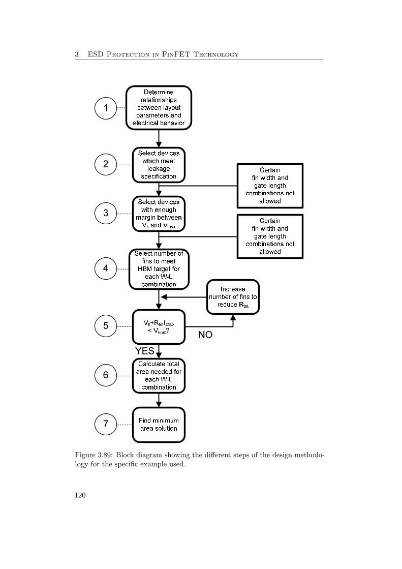
3. ESD Protection in FinFET Technology
Select devices which meet leakage specification Certainfin width andgate length combinations not allowedCertainfin width andgate length combinations not allowed
YES
Select devices with enough margin between Vh and VmaxSelect number of fins to meetHBM target for each W-L combinationVh+RtotIESD< Vmax?Calculate total area needed for each W-L combinationIncrease number of fins to reduce Rtot
Find minimum area solutionNO
Determine relationships between layout parameters andelectrical behavior1
2
3
4
5
6
7
Figure 3.89: Block diagram showing the different steps of the design methodo-logy for the specific example used.
120
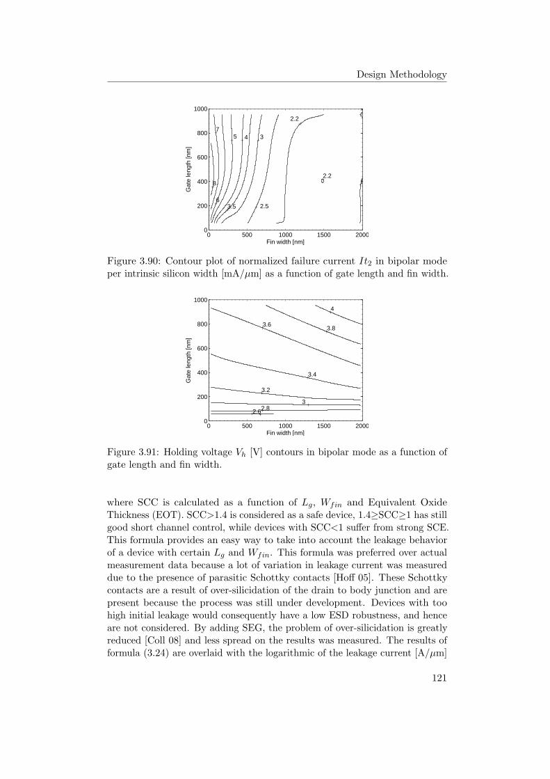
Design Methodology
2.2
2.2
2.2
2.2
2.5
3
3.5
45
6
7
8
Fin width [nm]
Gat
e le
ngth
[nm
]
0 500 1000 1500 20000
200
400
600
800
1000
Figure 3.90: Contour plot of normalized failure current It2 in bipolar modeper intrinsic silicon width [mA/µm] as a function of gate length and fin width.
2.62.83
3.2
3.4
3.63.8
4
Fin width [nm]
Gat
e le
ngth
[nm
]
0 500 1000 1500 20000
200
400
600
800
1000
Figure 3.91: Holding voltage Vh [V] contours in bipolar mode as a function ofgate length and fin width.
where SCC is calculated as a function of Lg, Wfin and Equivalent OxideThickness (EOT). SCC>1.4 is considered as a safe device, 1.4≥SCC≥1 has stillgood short channel control, while devices with SCC<1 suffer from strong SCE.This formula provides an easy way to take into account the leakage behaviorof a device with certain Lg and Wfin. This formula was preferred over actualmeasurement data because a lot of variation in leakage current was measureddue to the presence of parasitic Schottky contacts [Hoff 05]. These Schottkycontacts are a result of over-silicidation of the drain to body junction and arepresent because the process was still under development. Devices with toohigh initial leakage would consequently have a low ESD robustness, and henceare not considered. By adding SEG, the problem of over-silicidation is greatlyreduced [Coll 08] and less spread on the results was measured. The results offormula (3.24) are overlaid with the logarithmic of the leakage current [A/µm]
121
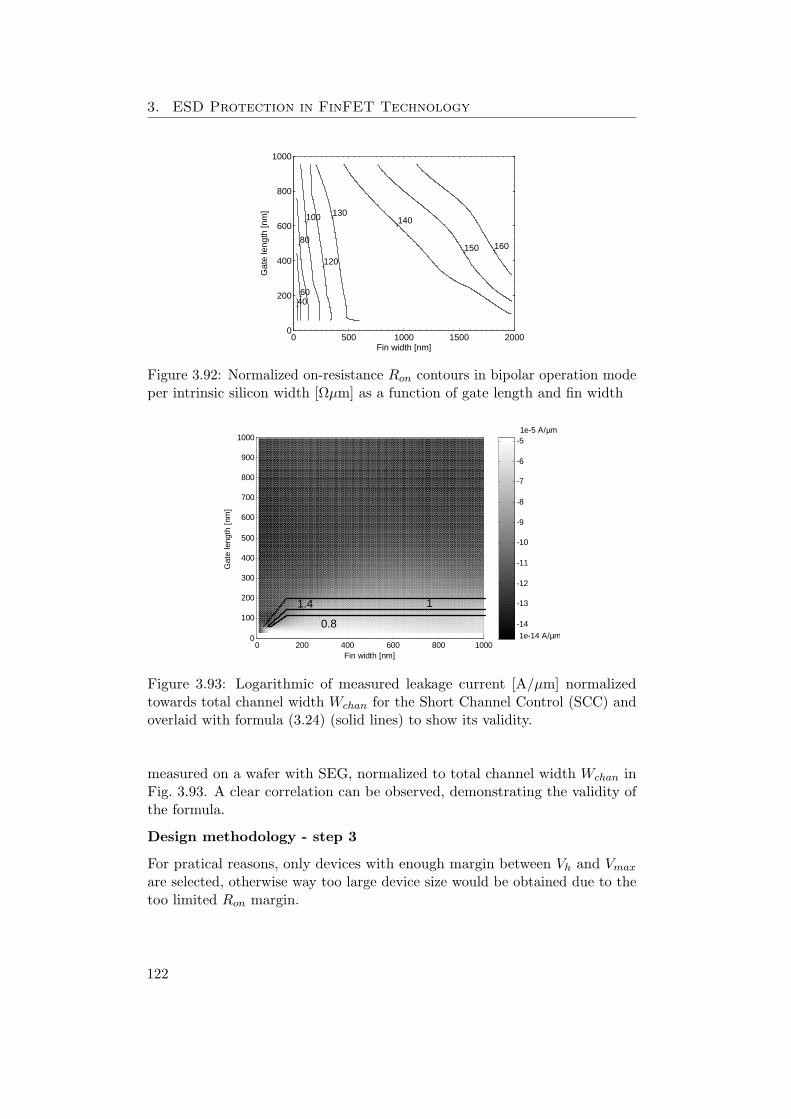
3. ESD Protection in FinFET Technology
4060
80
100
120
130140
150 160
Fin width [nm]
Gat
e le
ngth
[nm
]
0 500 1000 1500 20000
200
400
600
800
1000
Figure 3.92: Normalized on-resistance Ron contours in bipolar operation modeper intrinsic silicon width [Ωµm] as a function of gate length and fin width
0 200 400 600 800 10000
100
200
300
400
500
600
700
800
900
1000
1
Fin width [nm]
0.8
1.4
Gat
e le
ngth
[nm
]
-14
-13
-12
-11
-10
-9
-8
-7
-6
-51e-5 A/µm
1e-14 A/µm
Figure 3.93: Logarithmic of measured leakage current [A/µm] normalizedtowards total channel width Wchan for the Short Channel Control (SCC) andoverlaid with formula (3.24) (solid lines) to show its validity.
measured on a wafer with SEG, normalized to total channel width Wchan inFig. 3.93. A clear correlation can be observed, demonstrating the validity ofthe formula.
Design methodology - step 3
For pratical reasons, only devices with enough margin between Vh and Vmax
are selected, otherwise way too large device size would be obtained due to thetoo limited Ron margin.
122
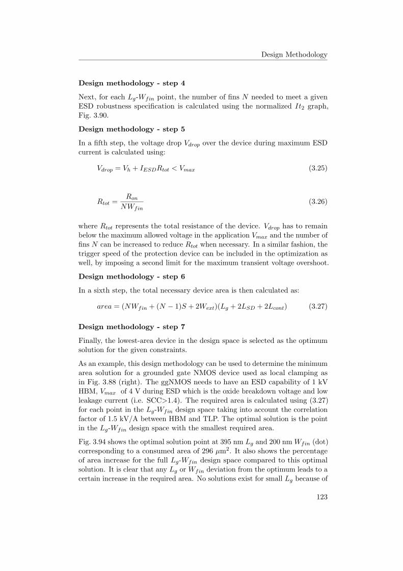
Design Methodology
Design methodology - step 4
Next, for each Lg-Wfin point, the number of fins N needed to meet a givenESD robustness specification is calculated using the normalized It2 graph,Fig. 3.90.
Design methodology - step 5
In a fifth step, the voltage drop Vdrop over the device during maximum ESDcurrent is calculated using:
Vdrop = Vh + IESDRtot < Vmax (3.25)
Rtot =Ron
NWfin(3.26)
where Rtot represents the total resistance of the device. Vdrop has to remainbelow the maximum allowed voltage in the application Vmax and the number offins N can be increased to reduce Rtot when necessary. In a similar fashion, thetrigger speed of the protection device can be included in the optimization aswell, by imposing a second limit for the maximum transient voltage overshoot.
Design methodology - step 6
In a sixth step, the total necessary device area is then calculated as:
area = (NWfin + (N − 1)S + 2Wext)(Lg + 2LSD + 2Lcont) (3.27)
Design methodology - step 7
Finally, the lowest-area device in the design space is selected as the optimumsolution for the given constraints.
As an example, this design methodology can be used to determine the minimumarea solution for a grounded gate NMOS device used as local clamping asin Fig. 3.88 (right). The ggNMOS needs to have an ESD capability of 1 kVHBM, Vmax of 4 V during ESD which is the oxide breakdown voltage and lowleakage current (i.e. SCC>1.4). The required area is calculated using (3.27)for each point in the Lg-Wfin design space taking into account the correlationfactor of 1.5 kV/A between HBM and TLP. The optimal solution is the pointin the Lg-Wfin design space with the smallest required area.
Fig. 3.94 shows the optimal solution point at 395 nm Lg and 200 nm Wfin (dot)corresponding to a consumed area of 296 µm2. It also shows the percentageof area increase for the full Lg-Wfin design space compared to this optimalsolution. It is clear that any Lg or Wfin deviation from the optimum leads to acertain increase in the required area. No solutions exist for small Lg because of
123
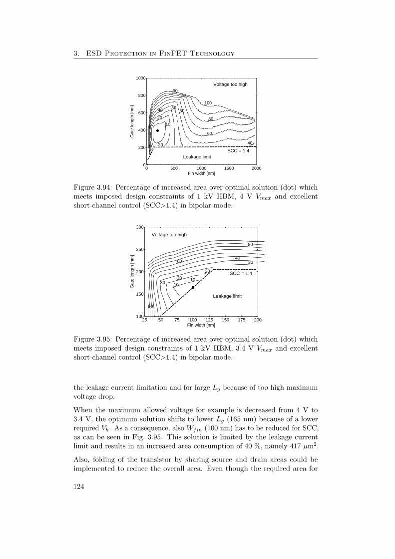
3. ESD Protection in FinFET Technology
10
20
20
3040
40
50
60
70
80
90
100
Fin width [nm]
Gat
e le
ngth
[nm
]
0 500 1000 1500 20000
200
400
600
800
1000
Voltage too high
SCC = 1.4Leakage limit
Figure 3.94: Percentage of increased area over optimal solution (dot) whichmeets imposed design constraints of 1 kV HBM, 4 V Vmax and excellentshort-channel control (SCC>1.4) in bipolar mode.
101020
20
30
3040
60
80
80
90
Fin width [nm]
Gat
e le
ngth
[nm
]
25 50 75 100 125 150 175 200100
150
200
250
300
Voltage too high
SCC = 1.4
Leakage limit
Figure 3.95: Percentage of increased area over optimal solution (dot) whichmeets imposed design constraints of 1 kV HBM, 3.4 V Vmax and excellentshort-channel control (SCC>1.4) in bipolar mode.
the leakage current limitation and for large Lg because of too high maximumvoltage drop.
When the maximum allowed voltage for example is decreased from 4 V to3.4 V, the optimum solution shifts to lower Lg (165 nm) because of a lowerrequired Vh. As a consequence, also Wfin (100 nm) has to be reduced for SCC,as can be seen in Fig. 3.95. This solution is limited by the leakage currentlimit and results in an increased area consumption of 40 %, namely 417 µm2.
Also, folding of the transistor by sharing source and drain areas could beimplemented to reduce the overall area. Even though the required area for
124
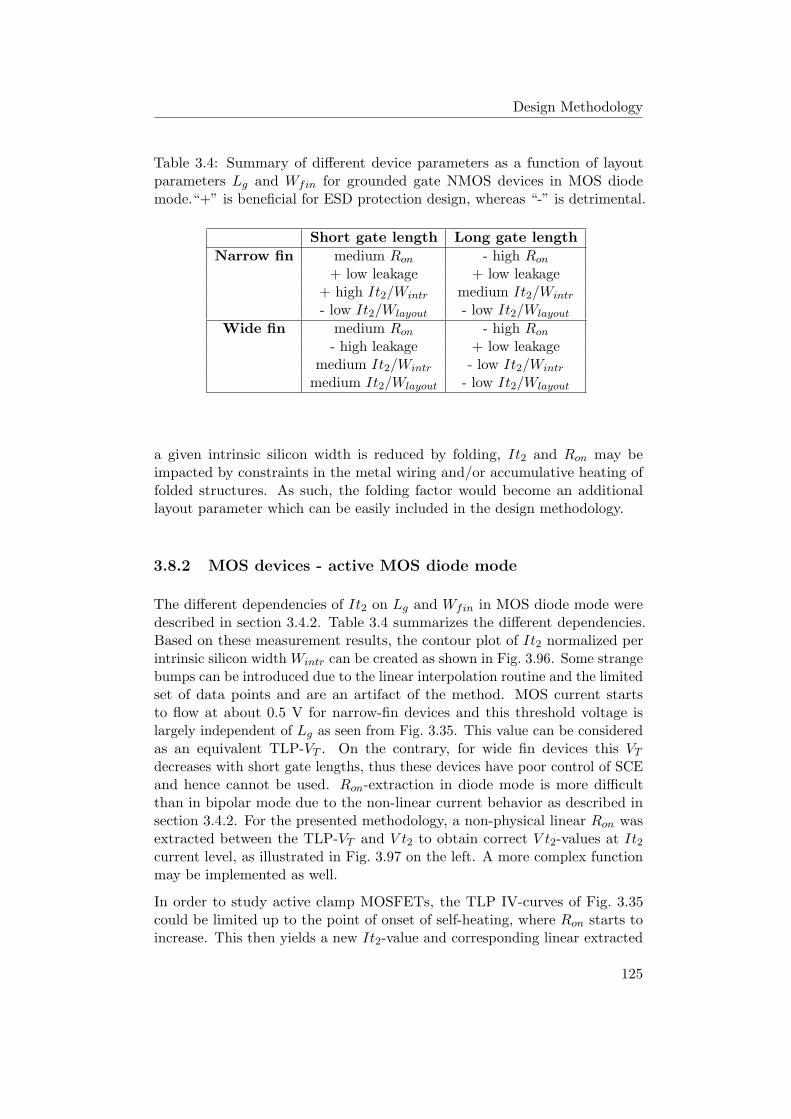
Design Methodology
Table 3.4: Summary of different device parameters as a function of layoutparameters Lg and Wfin for grounded gate NMOS devices in MOS diodemode.“+” is beneficial for ESD protection design, whereas “-” is detrimental.
Short gate length Long gate lengthNarrow fin medium Ron - high Ron
+ low leakage + low leakage+ high It2/Wintr medium It2/Wintr
- low It2/Wlayout - low It2/Wlayout
Wide fin medium Ron - high Ron
- high leakage + low leakagemedium It2/Wintr - low It2/Wintr
medium It2/Wlayout - low It2/Wlayout
a given intrinsic silicon width is reduced by folding, It2 and Ron may beimpacted by constraints in the metal wiring and/or accumulative heating offolded structures. As such, the folding factor would become an additionallayout parameter which can be easily included in the design methodology.
3.8.2 MOS devices - active MOS diode mode
The different dependencies of It2 on Lg and Wfin in MOS diode mode weredescribed in section 3.4.2. Table 3.4 summarizes the different dependencies.Based on these measurement results, the contour plot of It2 normalized perintrinsic silicon width Wintr can be created as shown in Fig. 3.96. Some strangebumps can be introduced due to the linear interpolation routine and the limitedset of data points and are an artifact of the method. MOS current startsto flow at about 0.5 V for narrow-fin devices and this threshold voltage islargely independent of Lg as seen from Fig. 3.35. This value can be consideredas an equivalent TLP-VT . On the contrary, for wide fin devices this VT
decreases with short gate lengths, thus these devices have poor control of SCEand hence cannot be used. Ron-extraction in diode mode is more difficultthan in bipolar mode due to the non-linear current behavior as described insection 3.4.2. For the presented methodology, a non-physical linear Ron wasextracted between the TLP-VT and V t2 to obtain correct V t2-values at It2current level, as illustrated in Fig. 3.97 on the left. A more complex functionmay be implemented as well.
In order to study active clamp MOSFETs, the TLP IV-curves of Fig. 3.35could be limited up to the point of onset of self-heating, where Ron starts toincrease. This then yields a new It2-value and corresponding linear extracted
125
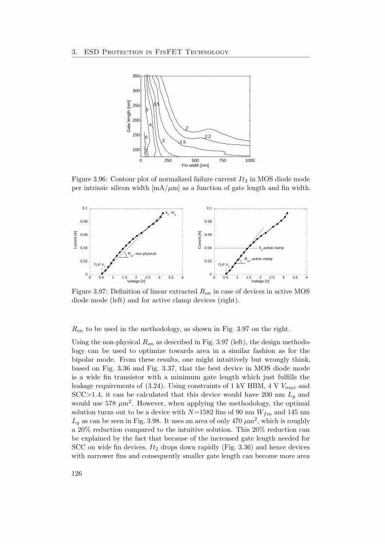
3. ESD Protection in FinFET Technology
2
2.22.53
3.5
4
5
6
7
Fin width [nm]
Gat
e le
ngth
[nm
]
0 250 500 750 1000
100
150
200
250
300
350
Figure 3.96: Contour plot of normalized failure current It2 in MOS diode modeper intrinsic silicon width [mA/µm] as a function of gate length and fin width.
0
0.02
0.04
0.06
0.08
0.1
0 0.5 1 1.5 2 2.5 3 3.5 4
Cur
rent
[A]
Voltage [V]
TLP VT
It2, Vt
2
Ron
, non-physical
0
0.02
0.04
0.06
0.08
0.1
0 0.5 1 1.5 2 2.5 3 3.5 4
Cur
rent
[A]
Voltage [V]
TLP VT
It2,active clamp
Ron
, active clamp
Figure 3.97: Definition of linear extracted Ron in case of devices in active MOSdiode mode (left) and for active clamp devices (right).
Ron to be used in the methodology, as shown in Fig. 3.97 on the right.
Using the non-physical Ron as described in Fig. 3.97 (left), the design methodo-logy can be used to optimize towards area in a similar fashion as for thebipolar mode. From these results, one might intuitively but wrongly think,based on Fig. 3.36 and Fig. 3.37, that the best device in MOS diode modeis a wide fin transistor with a minimum gate length which just fulfills theleakage requirements of (3.24). Using constraints of 1 kV HBM, 4 V Vmax andSCC>1.4, it can be calculated that this device would have 200 nm Lg andwould use 578 µm2. However, when applying the methodology, the optimalsolution turns out to be a device with N=1582 fins of 90 nm Wfin and 145 nmLg as can be seen in Fig. 3.98. It uses an area of only 470 µm2, which is roughlya 20% reduction compared to the intuitive solution. This 20% reduction canbe explained by the fact that because of the increased gate length needed forSCC on wide fin devices, It2 drops down rapidly (Fig. 3.36) and hence deviceswith narrower fins and consequently smaller gate length can become more area
126
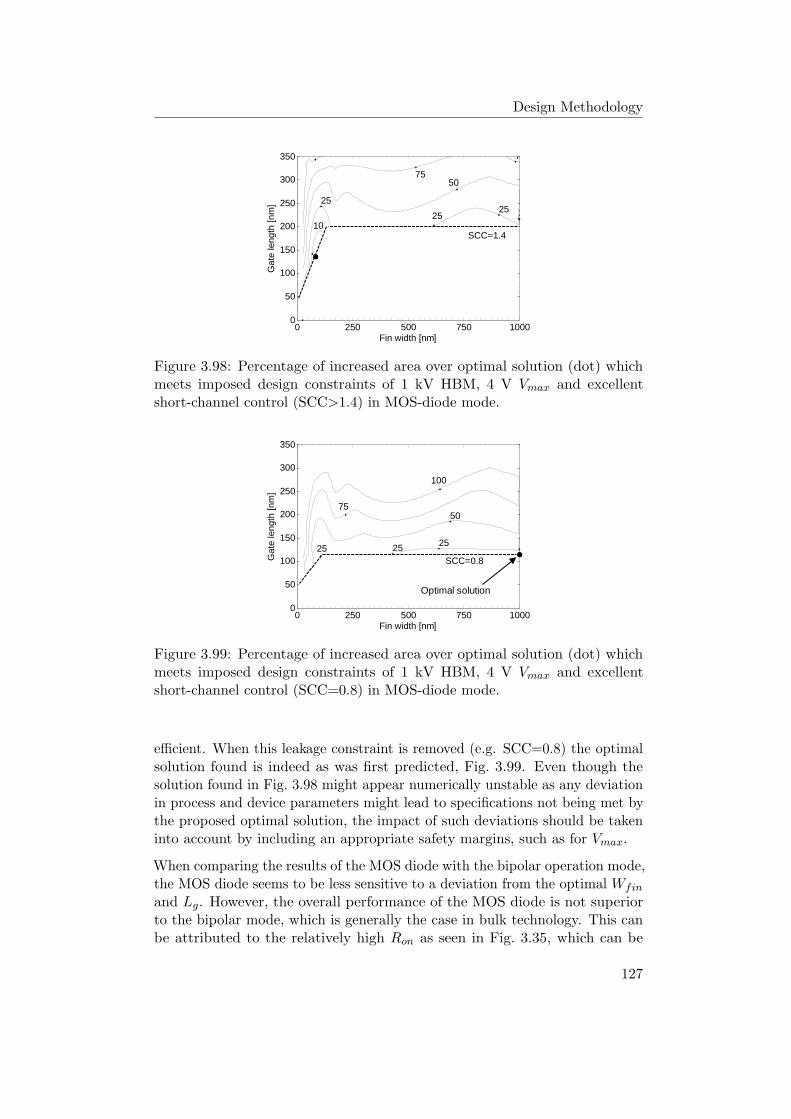
Design Methodology
1010
25
2525 25
5075
75100
Fin width [nm]
Gat
e le
ngth
[nm
]
0 250 500 750 10000
50
100
150
200
250
300
350
SCC=1.4
Figure 3.98: Percentage of increased area over optimal solution (dot) whichmeets imposed design constraints of 1 kV HBM, 4 V Vmax and excellentshort-channel control (SCC>1.4) in MOS-diode mode.
1025 25 25
5075
100
Fin width [nm]
Gat
e le
ngth
[nm
]
0 250 500 750 10000
50
100
150
200
250
300
350
Optimal solution
SCC=0.8
Figure 3.99: Percentage of increased area over optimal solution (dot) whichmeets imposed design constraints of 1 kV HBM, 4 V Vmax and excellentshort-channel control (SCC=0.8) in MOS-diode mode.
efficient. When this leakage constraint is removed (e.g. SCC=0.8) the optimalsolution found is indeed as was first predicted, Fig. 3.99. Even though thesolution found in Fig. 3.98 might appear numerically unstable as any deviationin process and device parameters might lead to specifications not being met bythe proposed optimal solution, the impact of such deviations should be takeninto account by including an appropriate safety margins, such as for Vmax.
When comparing the results of the MOS diode with the bipolar operation mode,the MOS diode seems to be less sensitive to a deviation from the optimal Wfin
and Lg. However, the overall performance of the MOS diode is not superiorto the bipolar mode, which is generally the case in bulk technology. This canbe attributed to the relatively high Ron as seen in Fig. 3.35, which can be
127
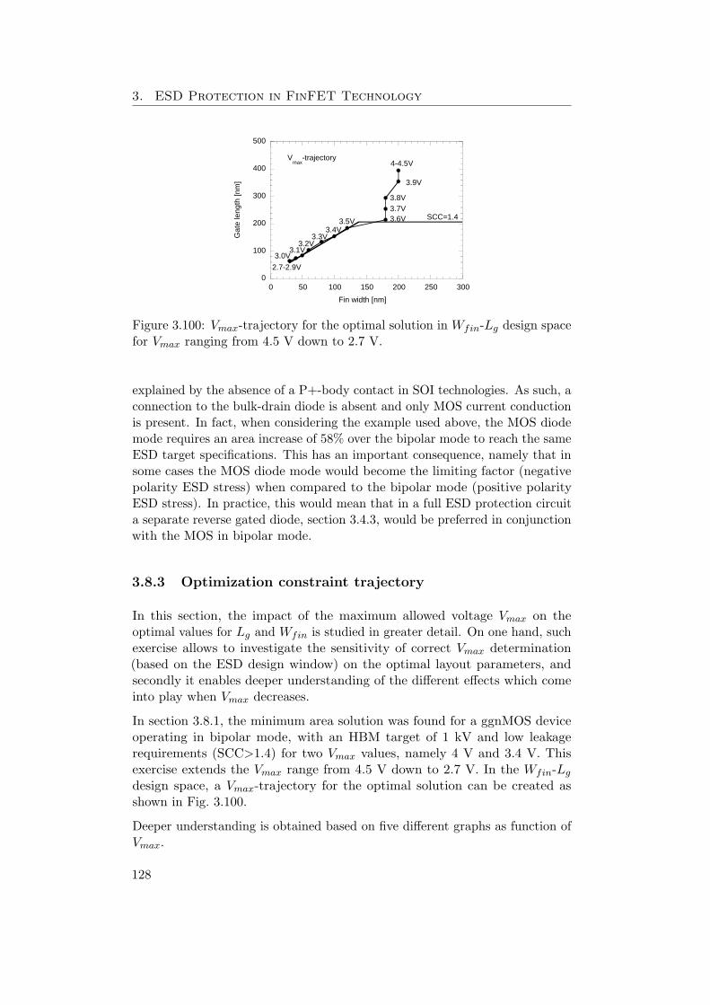
3. ESD Protection in FinFET Technology
0
100
200
300
400
500
0 50 100 150 200 250 300
Gat
e le
ngth
[nm
]
Fin width [nm]
Vmax
-trajectory4-4.5V
3.9V
3.8V3.7V3.6V3.5V
3.4V3.3V
3.2V3.1V
3.0V
2.7-2.9V
SCC=1.4
Figure 3.100: Vmax-trajectory for the optimal solution in Wfin-Lg design spacefor Vmax ranging from 4.5 V down to 2.7 V.
explained by the absence of a P+-body contact in SOI technologies. As such, aconnection to the bulk-drain diode is absent and only MOS current conductionis present. In fact, when considering the example used above, the MOS diodemode requires an area increase of 58% over the bipolar mode to reach the sameESD target specifications. This has an important consequence, namely that insome cases the MOS diode mode would become the limiting factor (negativepolarity ESD stress) when compared to the bipolar mode (positive polarityESD stress). In practice, this would mean that in a full ESD protection circuita separate reverse gated diode, section 3.4.3, would be preferred in conjunctionwith the MOS in bipolar mode.
3.8.3 Optimization constraint trajectory
In this section, the impact of the maximum allowed voltage Vmax on theoptimal values for Lg and Wfin is studied in greater detail. On one hand, suchexercise allows to investigate the sensitivity of correct Vmax determination(based on the ESD design window) on the optimal layout parameters, andsecondly it enables deeper understanding of the different effects which comeinto play when Vmax decreases.
In section 3.8.1, the minimum area solution was found for a ggnMOS deviceoperating in bipolar mode, with an HBM target of 1 kV and low leakagerequirements (SCC>1.4) for two Vmax values, namely 4 V and 3.4 V. Thisexercise extends the Vmax range from 4.5 V down to 2.7 V. In the Wfin-Lg
design space, a Vmax-trajectory for the optimal solution can be created asshown in Fig. 3.100.
Deeper understanding is obtained based on five different graphs as function ofVmax.
128
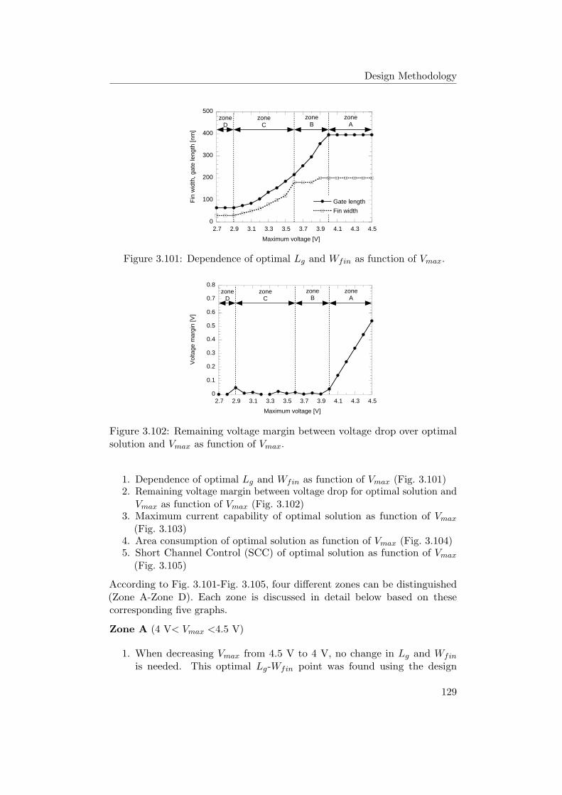
Design Methodology
0
100
200
300
400
500
2.7 2.9 3.1 3.3 3.5 3.7 3.9 4.1 4.3 4.5
Fin width
Gate lengthFin
wid
th, g
ate
leng
th [n
m]
Maximum voltage [V]
zoneD
zoneC
zoneB
zoneA
Figure 3.101: Dependence of optimal Lg and Wfin as function of Vmax.
0
0.1
0.2
0.3
0.4
0.5
0.6
0.7
0.8
2.7 2.9 3.1 3.3 3.5 3.7 3.9 4.1 4.3 4.5
Vol
tage
mar
gin
[V]
Maximum voltage [V]
zoneD
zoneC
zoneB
zoneA
Figure 3.102: Remaining voltage margin between voltage drop over optimalsolution and Vmax as function of Vmax.
1. Dependence of optimal Lg and Wfin as function of Vmax (Fig. 3.101)2. Remaining voltage margin between voltage drop for optimal solution and
Vmax as function of Vmax (Fig. 3.102)3. Maximum current capability of optimal solution as function of Vmax
(Fig. 3.103)4. Area consumption of optimal solution as function of Vmax (Fig. 3.104)5. Short Channel Control (SCC) of optimal solution as function of Vmax
(Fig. 3.105)
According to Fig. 3.101-Fig. 3.105, four different zones can be distinguished(Zone A-Zone D). Each zone is discussed in detail below based on thesecorresponding five graphs.
Zone A (4 V< Vmax <4.5 V)
1. When decreasing Vmax from 4.5 V to 4 V, no change in Lg and Wfin
is needed. This optimal Lg-Wfin point was found using the design
129
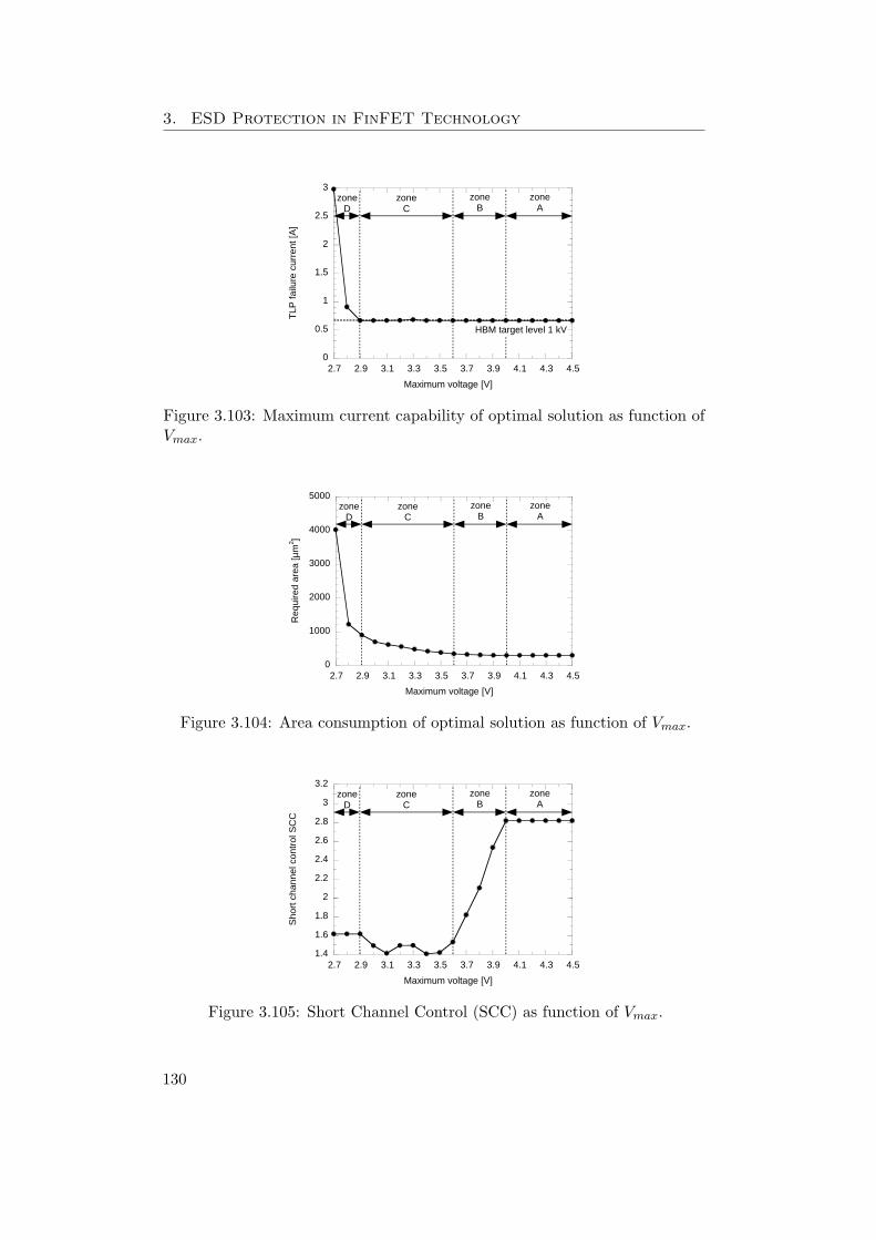
3. ESD Protection in FinFET Technology
0
0.5
1
1.5
2
2.5
3
2.7 2.9 3.1 3.3 3.5 3.7 3.9 4.1 4.3 4.5
TLP
failu
re c
urre
nt [A
]
Maximum voltage [V]
zoneD
zoneC
zoneB
zoneA
HBM target level 1 kV
Figure 3.103: Maximum current capability of optimal solution as function ofVmax.
0
1000
2000
3000
4000
5000
2.7 2.9 3.1 3.3 3.5 3.7 3.9 4.1 4.3 4.5
Req
uire
d ar
ea [µ
m2 ]
Maximum voltage [V]
zoneD
zoneC
zoneB
zoneA
Figure 3.104: Area consumption of optimal solution as function of Vmax.
1.4
1.6
1.8
2
2.2
2.4
2.6
2.8
3
3.2
2.7 2.9 3.1 3.3 3.5 3.7 3.9 4.1 4.3 4.5
Sho
rt c
hann
el c
ontr
ol S
CC
Maximum voltage [V]
zoneD
zoneC
zoneB
zoneA
Figure 3.105: Short Channel Control (SCC) as function of Vmax.
130

Design Methodology
methodology as shown in Fig. 3.94 and takes all the different dependenciesinto account.
2. This can be attributed to the fact that there is still margin left betweenthe voltage drop over the optimal solution during ESD and Vmax.
3. This optimal solution is limited by the minimum required ESD current(using correlation factor of 1.5 between TLP and HBM).
4. Since Lg and Wfin are not changing, the required area is independent ofVmax.
5. The solution is not limited by SCE, as SCC>1.4.
Zone B (3.6 V< Vmax <4 V)
1. When decreasing Vmax from 4 V to 3.6 V, Wfin stays constant, while Lg
needs to decrease.2. There is no voltage margin anymore, indicating that this solution is
limited by maximum voltage. This means that with reducing Vmax, alsoLg needs to be reduced to lower Vh, see Fig. 3.91.
3. The solution is limited by minimum required ESD current.4. The slight increase in area can be attributed to the decreasing Lg, which
causes a reduction of It2 and therefore a larger number of fins is needed,see Fig. 3.90.
5. The solution is not limited by SCE, meaning that for decreasing Lg,Wfin can remain constant.
Zone C (2.9 V< Vmax <3.6 V)
1. Both Wfin and Lg need to decrease when Vmax decreases from 3.6 V to2.9 V.
2. The solution is limited by maximum voltage requiring reduced Lg fordecreasing Vmax as in Zone B.
3. The solution is limited by minimum required ESD current.4. Area consumption increases more and more since Wfin is decreasing also,
next to Lg as in Zone B. This leads to less area efficiency by increasedoverhead due to fin-to-fin spacing.
5. Additionaly over Zone B, as SCC=1.4, this solution is limited by SCE,as can also be seen from Fig. 3.100. This requires a decrease in Wfin fordecreasing Lg. (The deviation of SCC=1.4 is due to quantized values forLg and Wfin, with a 5 nm resolution.)
Zone D (2.7 V< Vmax <2.9 V)
1. Lg and Wfin stay constant when Vmax decreases from 2.9 V to 2.7 Vsince the minimum fin width of 30 nm is reached.
2. The solution is limited by maximum voltage.
131
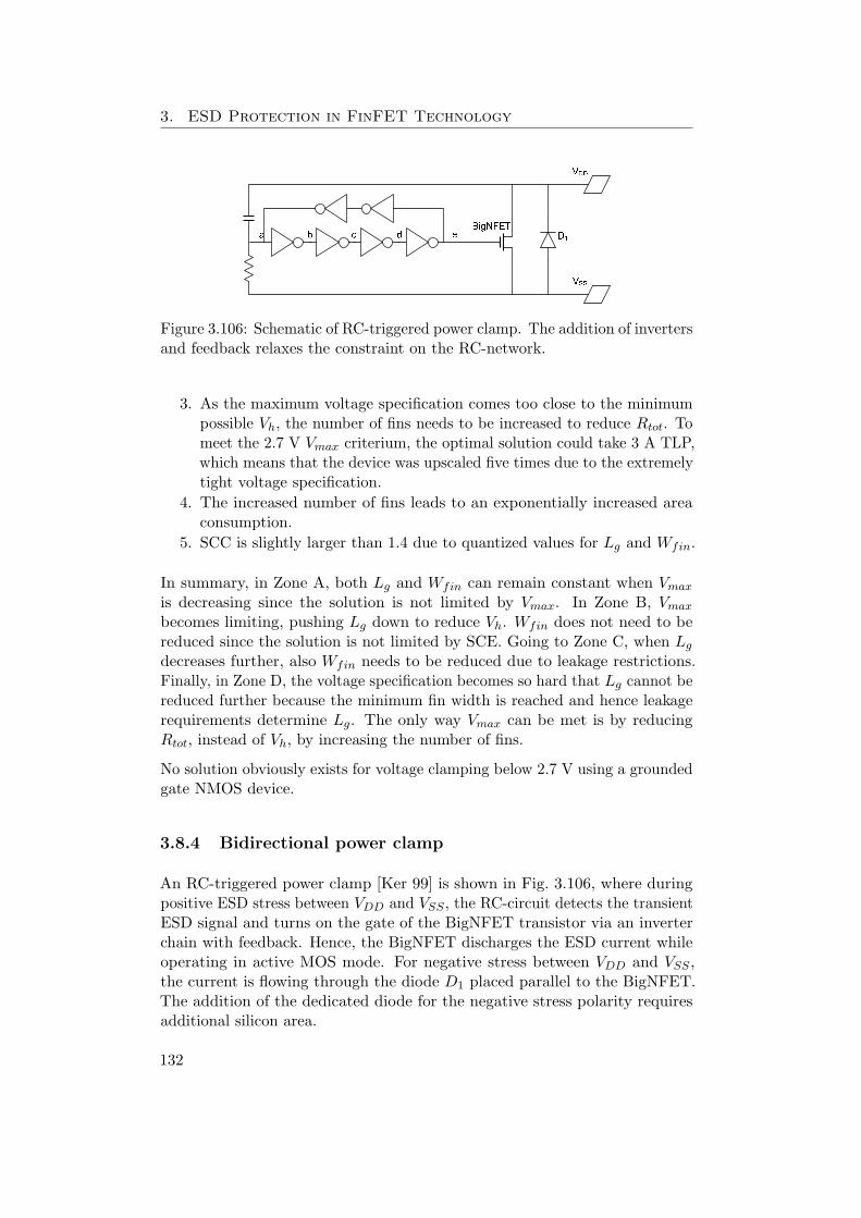
3. ESD Protection in FinFET Technology
BigNFET VDDVSSa b c d e D1
Figure 3.106: Schematic of RC-triggered power clamp. The addition of invertersand feedback relaxes the constraint on the RC-network.
3. As the maximum voltage specification comes too close to the minimumpossible Vh, the number of fins needs to be increased to reduce Rtot. Tomeet the 2.7 V Vmax criterium, the optimal solution could take 3 A TLP,which means that the device was upscaled five times due to the extremelytight voltage specification.
4. The increased number of fins leads to an exponentially increased areaconsumption.
5. SCC is slightly larger than 1.4 due to quantized values for Lg and Wfin.
In summary, in Zone A, both Lg and Wfin can remain constant when Vmax
is decreasing since the solution is not limited by Vmax. In Zone B, Vmax
becomes limiting, pushing Lg down to reduce Vh. Wfin does not need to bereduced since the solution is not limited by SCE. Going to Zone C, when Lg
decreases further, also Wfin needs to be reduced due to leakage restrictions.Finally, in Zone D, the voltage specification becomes so hard that Lg cannot bereduced further because the minimum fin width is reached and hence leakagerequirements determine Lg. The only way Vmax can be met is by reducingRtot, instead of Vh, by increasing the number of fins.
No solution obviously exists for voltage clamping below 2.7 V using a groundedgate NMOS device.
3.8.4 Bidirectional power clamp
An RC-triggered power clamp [Ker 99] is shown in Fig. 3.106, where duringpositive ESD stress between VDD and VSS , the RC-circuit detects the transientESD signal and turns on the gate of the BigNFET transistor via an inverterchain with feedback. Hence, the BigNFET discharges the ESD current whileoperating in active MOS mode. For negative stress between VDD and VSS ,the current is flowing through the diode D1 placed parallel to the BigNFET.The addition of the dedicated diode for the negative stress polarity requiresadditional silicon area.
132
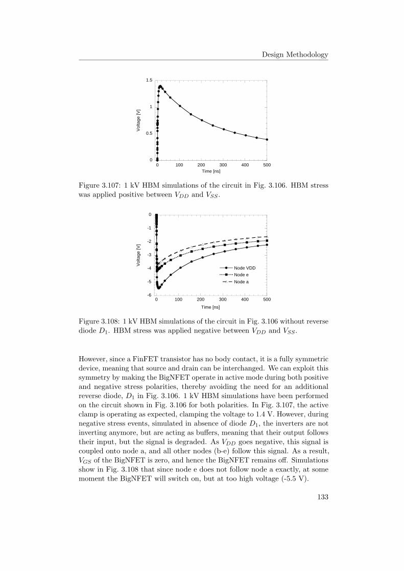
Design Methodology
0
0.5
1
1.5
0 100 200 300 400 500
Vol
tage
[V]
Time [ns]
Figure 3.107: 1 kV HBM simulations of the circuit in Fig. 3.106. HBM stresswas applied positive between VDD and VSS .
-6
-5
-4
-3
-2
-1
0
0 100 200 300 400 500
Node a
Node e
Node VDD
Vol
tage
[V]
Time [ns]
Figure 3.108: 1 kV HBM simulations of the circuit in Fig. 3.106 without reversediode D1. HBM stress was applied negative between VDD and VSS .
However, since a FinFET transistor has no body contact, it is a fully symmetricdevice, meaning that source and drain can be interchanged. We can exploit thissymmetry by making the BigNFET operate in active mode during both positiveand negative stress polarities, thereby avoiding the need for an additionalreverse diode, D1 in Fig. 3.106. 1 kV HBM simulations have been performedon the circuit shown in Fig. 3.106 for both polarities. In Fig. 3.107, the activeclamp is operating as expected, clamping the voltage to 1.4 V. However, duringnegative stress events, simulated in absence of diode D1, the inverters are notinverting anymore, but are acting as buffers, meaning that their output followstheir input, but the signal is degraded. As VDD goes negative, this signal iscoupled onto node a, and all other nodes (b-e) follow this signal. As a result,VGS of the BigNFET is zero, and hence the BigNFET remains off. Simulationsshow in Fig. 3.108 that since node e does not follow node a exactly, at somemoment the BigNFET will switch on, but at too high voltage (-5.5 V).
133
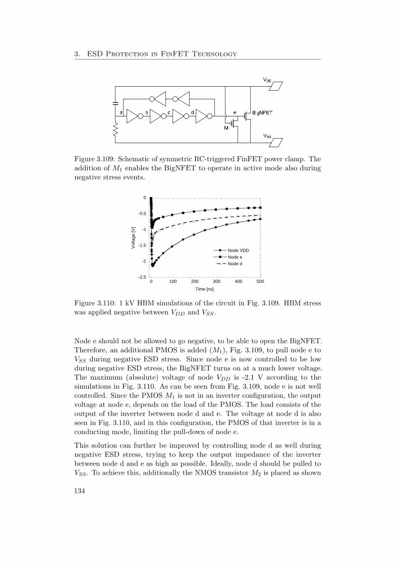
3. ESD Protection in FinFET Technology
BigNFETVDDVSSM1a b c d e
Figure 3.109: Schematic of symmetric RC-triggered FinFET power clamp. Theaddition of M1 enables the BigNFET to operate in active mode also duringnegative stress events.
-2.5
-2
-1.5
-1
-0.5
0
0 100 200 300 400 500
Node VDD
Node e
Node d
Vol
tage
[V]
Time [ns]
Figure 3.110: 1 kV HBM simulations of the circuit in Fig. 3.109. HBM stresswas applied negative between VDD and VSS .
Node e should not be allowed to go negative, to be able to open the BigNFET.Therefore, an additional PMOS is added (M1), Fig. 3.109, to pull node e toVSS during negative ESD stress. Since node e is now controlled to be lowduring negative ESD stress, the BigNFET turns on at a much lower voltage.The maximum (absolute) voltage of node VDD is -2.1 V according to thesimulations in Fig. 3.110. As can be seen from Fig. 3.109, node e is not wellcontrolled. Since the PMOS M1 is not in an inverter configuration, the outputvoltage at node e, depends on the load of the PMOS. The load consists of theoutput of the inverter between node d and e. The voltage at node d is alsoseen in Fig. 3.110, and in this configuration, the PMOS of that inverter is in aconducting mode, limiting the pull-down of node e.
This solution can further be improved by controlling node d as well duringnegative ESD stress, trying to keep the output impedance of the inverterbetween node d and e as high as possible. Ideally, node d should be pulled toVSS . To achieve this, additionally the NMOS transistor M2 is placed as shown
134
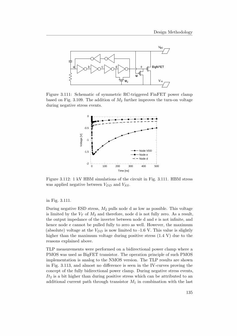
Design Methodology
BigNFETVDDVSSM1M2a b c d e
Figure 3.111: Schematic of symmetric RC-triggered FinFET power clampbased on Fig. 3.109. The addition of M2 further improves the turn-on voltageduring negative stress events.
-2
-1.5
-1
-0.5
0
0 100 200 300 400 500
Node VDD
Node e
Node d
Vol
tage
[V]
Time [ns]
Figure 3.112: 1 kV HBM simulations of the circuit in Fig. 3.111. HBM stresswas applied negative between VDD and VSS .
in Fig. 3.111.
During negative ESD stress, M2 pulls node d as low as possible. This voltageis limited by the VT of M2 and therefore, node d is not fully zero. As a result,the output impedance of the inverter between node d and e is not infinite, andhence node e cannot be pulled fully to zero as well. However, the maximum(absolute) voltage at the VDD is now limited to -1.6 V. This value is slightlyhigher than the maximum voltage during positive stress (1.4 V) due to thereasons explained above.
TLP measurements were performed on a bidirectional power clamp where aPMOS was used as BigFET transistor. The operation principle of such PMOSimplementation is analog to the NMOS version. The TLP results are shownin Fig. 3.113, and almost no difference is seen in the IV-curves proving theconcept of the fully bidirectional power clamp. During negative stress events,It2 is a bit higher than during positive stress which can be attributed to anadditional current path through transistor M1 in combination with the last
135
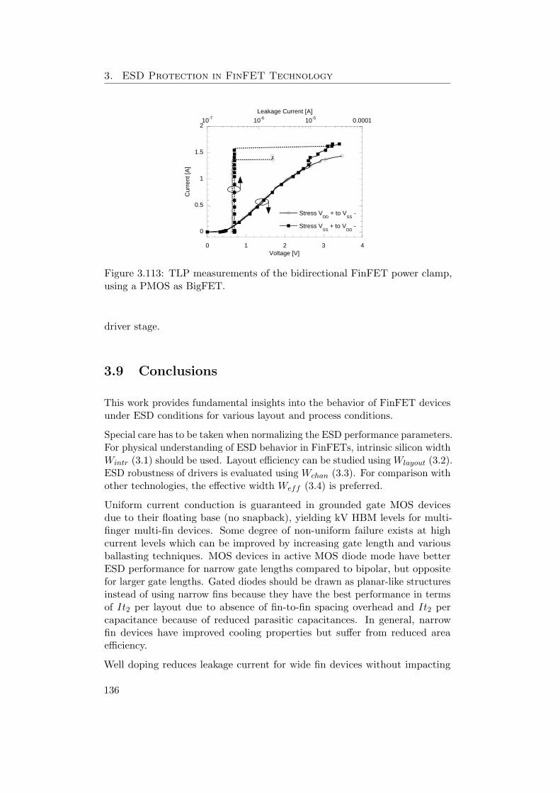
3. ESD Protection in FinFET Technology
0
0.5
1
1.5
2
0 1 2 3 4
10-7 10-6 10-5 0.0001
Stress VDD
+ to VSS
-
Stress VSS
+ to VDD
-
Cur
rent
[A]
Voltage [V]
Leakage Current [A]
Figure 3.113: TLP measurements of the bidirectional FinFET power clamp,using a PMOS as BigFET.
driver stage.
3.9 Conclusions
This work provides fundamental insights into the behavior of FinFET devicesunder ESD conditions for various layout and process conditions.
Special care has to be taken when normalizing the ESD performance parameters.For physical understanding of ESD behavior in FinFETs, intrinsic silicon widthWintr (3.1) should be used. Layout efficiency can be studied using Wlayout (3.2).ESD robustness of drivers is evaluated using Wchan (3.3). For comparison withother technologies, the effective width Weff (3.4) is preferred.
Uniform current conduction is guaranteed in grounded gate MOS devicesdue to their floating base (no snapback), yielding kV HBM levels for multi-finger multi-fin devices. Some degree of non-uniform failure exists at highcurrent levels which can be improved by increasing gate length and variousballasting techniques. MOS devices in active MOS diode mode have betterESD performance for narrow gate lengths compared to bipolar, but oppositefor larger gate lengths. Gated diodes should be drawn as planar-like structuresinstead of using narrow fins because they have the best performance in termsof It2 per layout due to absence of fin-to-fin spacing overhead and It2 percapacitance because of reduced parasitic capacitances. In general, narrowfin devices have improved cooling properties but suffer from reduced areaefficiency.
Well doping reduces leakage current for wide fin devices without impacting
136
Conclusions
ESD performance. SEG drastically improves It2 and Ron and removes anyoversilicidation problems. Also Silicide Blocking removes the oversilicidationeffect. It further improves It2 due to improved failure current uniformity atthe expense of increased Ron. Strain also increases It2 by improving the carriermobility and by improving failure uniformity. FinFET technology developmentis still facing a lot of process challenges which have a direct impact on theESD performance of the devices.
A FinFET design methodology is required to find the solution for a multi-dimensional optimization problem depending on functional and ESD limitations.The developed methodology yields the optimal design solution, which wasfound to be sensitive to layout and process deviations. The absence of a bodycontact for the MOS device in diode mode can make it less efficient than inbipolar mode for a given set of constraints.
All the results demonstrate that the possible extreme sensitivity of FinFETdevices would not be a showstopper for the advanced nanotechnologies if ESDis considered during the technology development. However, even with thisknowledge, the design of ESD protection for FinFET technology appears to bea challenging task in the future.
137

Chapter 4
ESD Protection forNarrowband RF CMOSCircuits
The traditional low-capacitance RF-ESD protection approach is not feasibleanymore for narrowband RF circuits operating at frequencies >5 GHz. Induc-tive based ESD protection is an excellent alternative solution which improveswith increasing frequency in terms of RF performance, ESD performance (bothHBM and CDM) and area consumption. This technique has been validatedon a number of case studies, including Low Noise Amplifier (LNA) and PowerAmplifier (PA) designs implemented in 90 nm, 45 nm planar and 45 nm FinFETCMOS technologies for operating frequencies ranging from 5 GHz to 60 GHz.
4.1 Introduction
Emergence of extensive applications for portable electronics has fueled therapid deployment of CMOS based integrated RF front-ends. These technologiesdemonstrated transit frequencies well above 150 GHz, e.g. in a 90 nm CMOStechnology, and are commercially available for manufacturing. This chapterfocusses on ESD protection for narrowband RF circuits. Chapter 5 discussesin a similar way wideband RF circuits.
In an RF front-end, the LNA is one of the critical building blocks. TheLNA, being connected to the outside world through its antenna can thereforeeasily be exposed to ESD stress events. Incorporating sufficient and suitableESD protection on the LNA requires that the added ESD protection does notdegrade the designed functional performance parameters of the LNA. Themost important performance figures for the LNA along with a typical target
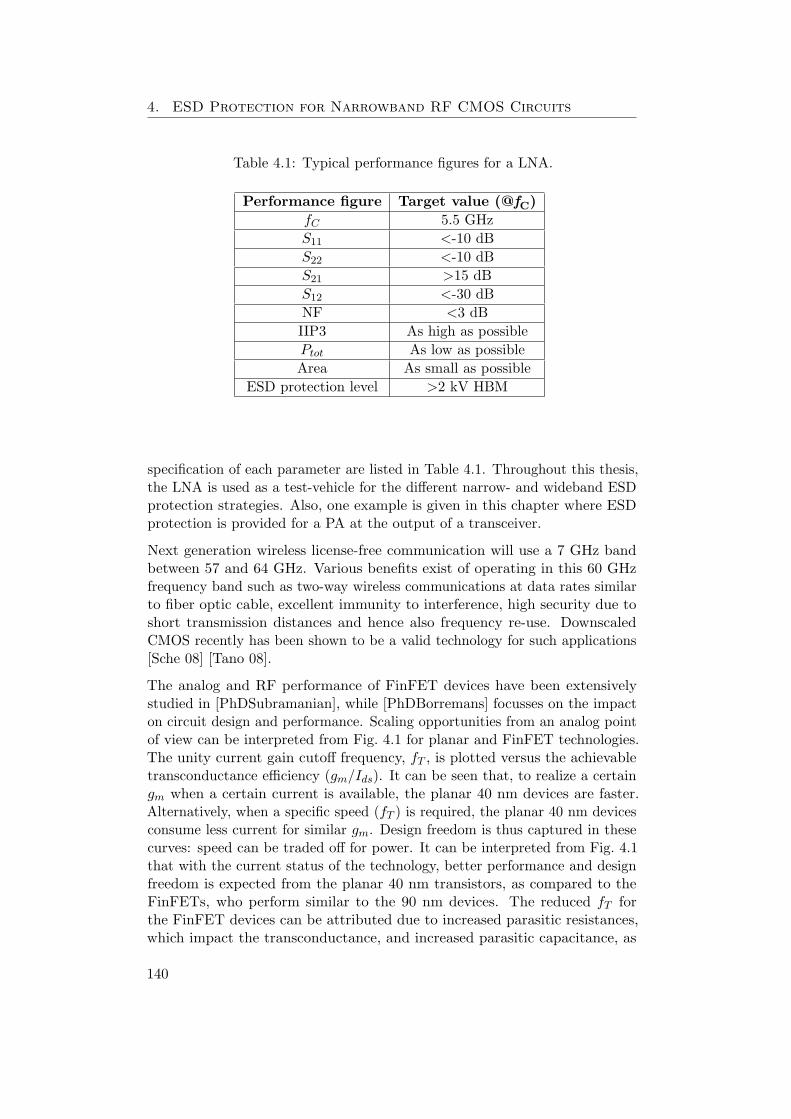
4. ESD Protection for Narrowband RF CMOS Circuits
Table 4.1: Typical performance figures for a LNA.
Performance figure Target value (@fC)fC 5.5 GHzS11 <-10 dBS22 <-10 dBS21 >15 dBS12 <-30 dBNF <3 dBIIP3 As high as possiblePtot As low as possibleArea As small as possible
ESD protection level >2 kV HBM
specification of each parameter are listed in Table 4.1. Throughout this thesis,the LNA is used as a test-vehicle for the different narrow- and wideband ESDprotection strategies. Also, one example is given in this chapter where ESDprotection is provided for a PA at the output of a transceiver.
Next generation wireless license-free communication will use a 7 GHz bandbetween 57 and 64 GHz. Various benefits exist of operating in this 60 GHzfrequency band such as two-way wireless communications at data rates similarto fiber optic cable, excellent immunity to interference, high security due toshort transmission distances and hence also frequency re-use. DownscaledCMOS recently has been shown to be a valid technology for such applications[Sche 08] [Tano 08].
The analog and RF performance of FinFET devices have been extensivelystudied in [PhDSubramanian], while [PhDBorremans] focusses on the impacton circuit design and performance. Scaling opportunities from an analog pointof view can be interpreted from Fig. 4.1 for planar and FinFET technologies.The unity current gain cutoff frequency, fT , is plotted versus the achievabletransconductance efficiency (gm/Ids). It can be seen that, to realize a certaingm when a certain current is available, the planar 40 nm devices are faster.Alternatively, when a specific speed (fT ) is required, the planar 40 nm devicesconsume less current for similar gm. Design freedom is thus captured in thesecurves: speed can be traded off for power. It can be interpreted from Fig. 4.1that with the current status of the technology, better performance and designfreedom is expected from the planar 40 nm transistors, as compared to theFinFETs, who perform similar to the 90 nm devices. The reduced fT forthe FinFET devices can be attributed due to increased parasitic resistances,which impact the transconductance, and increased parasitic capacitance, as
140
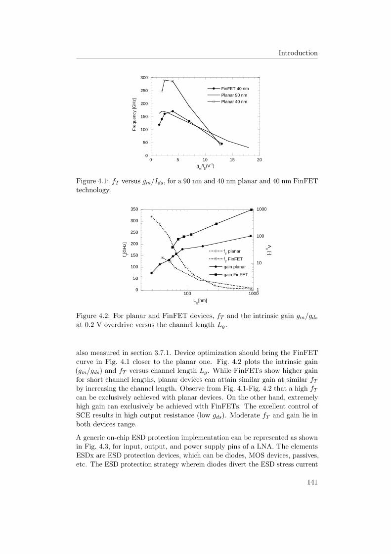
Introduction
0 5 10 15 20
FinFET 40 nm
Planar 90 nm
Planar 40 nm
0
50
100
150
200
250
300
Fre
quen
cy [G
Hz]
gm
/ID(V-1)
Figure 4.1: fT versus gm/Ids, for a 90 nm and 40 nm planar and 40 nm FinFETtechnology.
0
50
100
150
200
250
300
350
1
10
100
1000
100 1000
fT planar
fT FinFET
gain planar
gain FinFET
f T[G
Hz] A
V [-]
LG[nm]
Figure 4.2: For planar and FinFET devices, fT and the intrinsic gain gm/gds
at 0.2 V overdrive versus the channel length Lg.
also measured in section 3.7.1. Device optimization should bring the FinFETcurve in Fig. 4.1 closer to the planar one. Fig. 4.2 plots the intrinsic gain(gm/gds) and fT versus channel length Lg. While FinFETs show higher gainfor short channel lengths, planar devices can attain similar gain at similar fT
by increasing the channel length. Observe from Fig. 4.1-Fig. 4.2 that a high fT
can be exclusively achieved with planar devices. On the other hand, extremelyhigh gain can exclusively be achieved with FinFETs. The excellent control ofSCE results in high output resistance (low gds). Moderate fT and gain lie inboth devices range.
A generic on-chip ESD protection implementation can be represented as shownin Fig. 4.3, for input, output, and power supply pins of a LNA. The elementsESDx are ESD protection devices, which can be diodes, MOS devices, passives,etc. The ESD protection strategy wherein diodes divert the ESD stress current
141
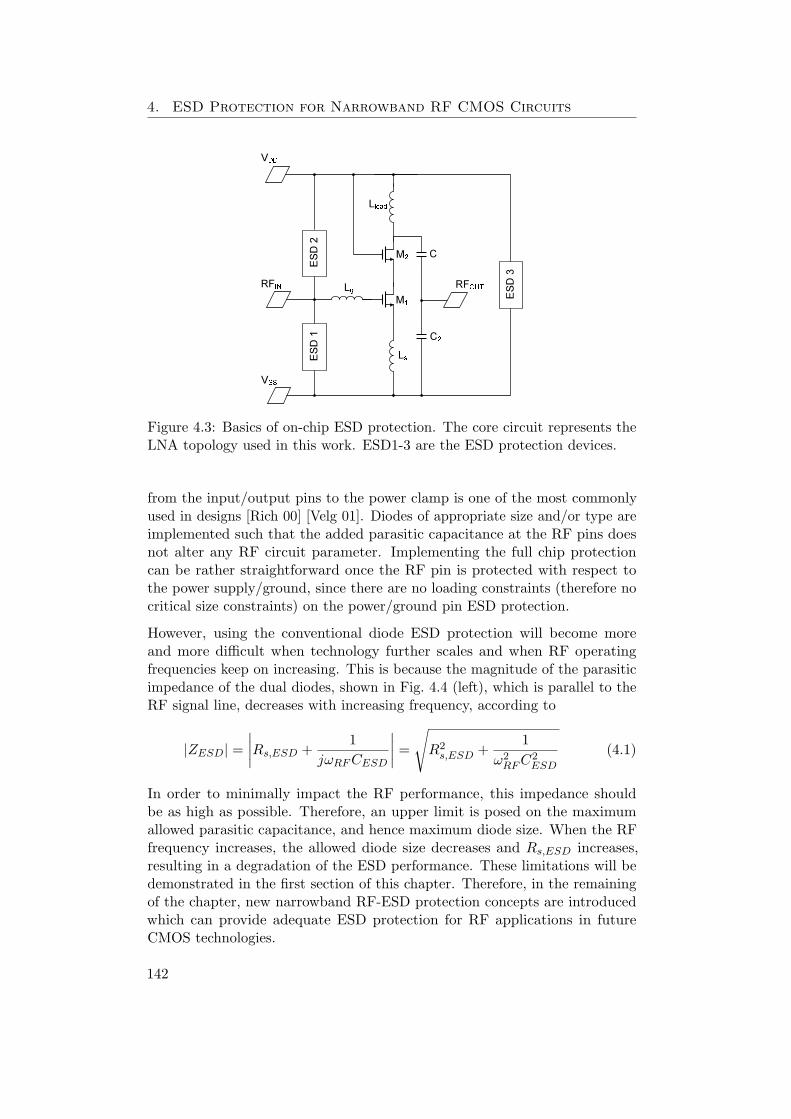
4. ESD Protection for Narrowband RF CMOS Circuits
LsLg
M1M2Lload
C2RFIN RFOUTC1
ESD
2ES
D 1
ESD
3
VDD
VSSFigure 4.3: Basics of on-chip ESD protection. The core circuit represents theLNA topology used in this work. ESD1-3 are the ESD protection devices.
from the input/output pins to the power clamp is one of the most commonlyused in designs [Rich 00] [Velg 01]. Diodes of appropriate size and/or type areimplemented such that the added parasitic capacitance at the RF pins doesnot alter any RF circuit parameter. Implementing the full chip protectioncan be rather straightforward once the RF pin is protected with respect tothe power supply/ground, since there are no loading constraints (therefore nocritical size constraints) on the power/ground pin ESD protection.
However, using the conventional diode ESD protection will become moreand more difficult when technology further scales and when RF operatingfrequencies keep on increasing. This is because the magnitude of the parasiticimpedance of the dual diodes, shown in Fig. 4.4 (left), which is parallel to theRF signal line, decreases with increasing frequency, according to
|ZESD| =∣∣∣∣Rs,ESD +
1jωRF CESD
∣∣∣∣ =
√R2
s,ESD +1
ω2RF C2
ESD
(4.1)
In order to minimally impact the RF performance, this impedance shouldbe as high as possible. Therefore, an upper limit is posed on the maximumallowed parasitic capacitance, and hence maximum diode size. When the RFfrequency increases, the allowed diode size decreases and Rs,ESD increases,resulting in a degradation of the ESD performance. These limitations will bedemonstrated in the first section of this chapter. Therefore, in the remainingof the chapter, new narrowband RF-ESD protection concepts are introducedwhich can provide adequate ESD protection for RF applications in futureCMOS technologies.
142
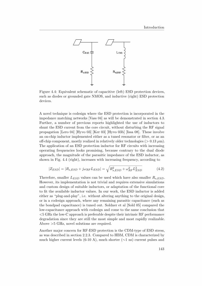
Introduction
LESDCESDRs,ESD Rs,ESD
Figure 4.4: Equivalent schematic of capacitive (left) ESD protection devices,such as diodes or grounded gate NMOS, and inductive (right) ESD protectiondevices.
A novel technique is codesign where the ESD protection is incorporated in theimpedance matching networks [Vass 04] as will be demonstrated in section 4.3.Further, a number of previous reports highlighted the use of inductors toshunt the ESD current from the core circuit, without disturbing the RF signalpropagation [Lero 04] [Hyvo 03] [Ker 03] [Hyvo 03b] [Issa 08]. These involvean on-chip inductor implemented either as a tuned resonator or filter, or as anoff-chip component, mostly realized in relatively older technologies (> 0.13 µm).The application of an ESD protection inductor for RF circuits with increasingoperating frequencies looks promising, because contrary to the dual diodeapproach, the magnitude of the parasitic impedance of the ESD inductor, asshown in Fig. 4.4 (right), increases with increasing frequency, according to
|ZESD| = |Rs,ESD + jωRF LESD| =√
R2s,ESD + ω2
RF L2ESD (4.2)
Therefore, smaller LESD values can be used which have also smaller Rs,ESD.However, its implementation is not trivial and requires extensive simulationsand custom design of suitable inductors, or adaptation of the functional coreto fit the available inductor values. In our work, the ESD inductor is addedeither as “plug-and-play”, i.e. without altering anything to the original design,or in a codesign approach, where any remaining parasitic capacitance (such asthe bondpad capacitance) is tuned out. Soldner et al [Sold 05] compared thelow-capacitance approach with codesign and come to the same conclusion that<5 GHz the low-C approach is preferable despite their intrinsic RF performancedegradation since they are still the most simple and most rapidly realizable.Above >5 GHz, novel solutions are required.
Another major concern for RF-ESD protection is the CDM-type of ESD stress,as was described in section 2.2.3. Compared to HBM, CDM is characterized bymuch higher current levels (6-10 A), much shorter (∼1 ns) current pulses and
143
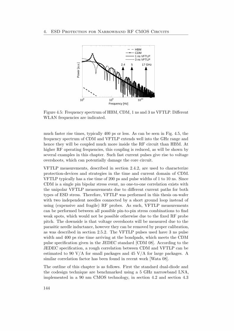
4. ESD Protection for Narrowband RF CMOS Circuits
108 109 1010
HBMCDM1 ns VFTLP3 ns VFTLP
Pow
er [a
.u.]
Frequency [Hz]
2.4 5 17 GHz
Figure 4.5: Frequency spectrum of HBM, CDM, 1 ns and 3 ns VFTLP. DifferentWLAN frequencies are indicated.
much faster rise times, typically 400 ps or less. As can be seen in Fig. 4.5, thefrequency spectrum of CDM and VFTLP extends well into the GHz range andhence they will be coupled much more inside the RF circuit than HBM. Athigher RF operating frequencies, this coupling is reduced, as will be shown byseveral examples in this chapter. Such fast current pulses give rise to voltageovershoots, which can potentially damage the core circuit.
VFTLP measurements, described in section 2.4.2, are used to characterizeprotection-devices and strategies in the time and current domain of CDM.VFTLP typically has a rise time of 200 ps and pulse widths of 1 to 10 ns. SinceCDM is a single pin bipolar stress event, no one-to-one correlation exists withthe unipolar VFTLP measurements due to different current paths for bothtypes of ESD stress. Therefore, VFTLP was performed in this thesis on-waferwith two independent needles connected by a short ground loop instead ofusing (expensive and fragile) RF probes. As such, VFTLP measurementscan be performed between all possible pin-to-pin stress combinations to findweak spots, which would not be possible otherwise due to the fixed RF probepitch. The downside is that voltage overshoots will be measured due to theparasitic needle inductance, however they can be removed by proper calibration,as was described in section 2.5.2. The VFTLP pulses used have 3 ns pulsewidth and 400 ps rise time arriving at the bondpads, which meets the CDMpulse specification given in the JEDEC standard [CDM 08]. According to theJEDEC specification, a rough correlation between CDM and VFTLP can beestimated to 90 V/A for small packages and 45 V/A for large packages. Asimilar correlation factor has been found in recent work [Wata 08].
The outline of this chapter is as follows. First the standard dual-diode andthe codesign technique are benchmarked using a 5 GHz narrowband LNA,implemented in a 90 nm CMOS technology, in section 4.2 and section 4.3
144
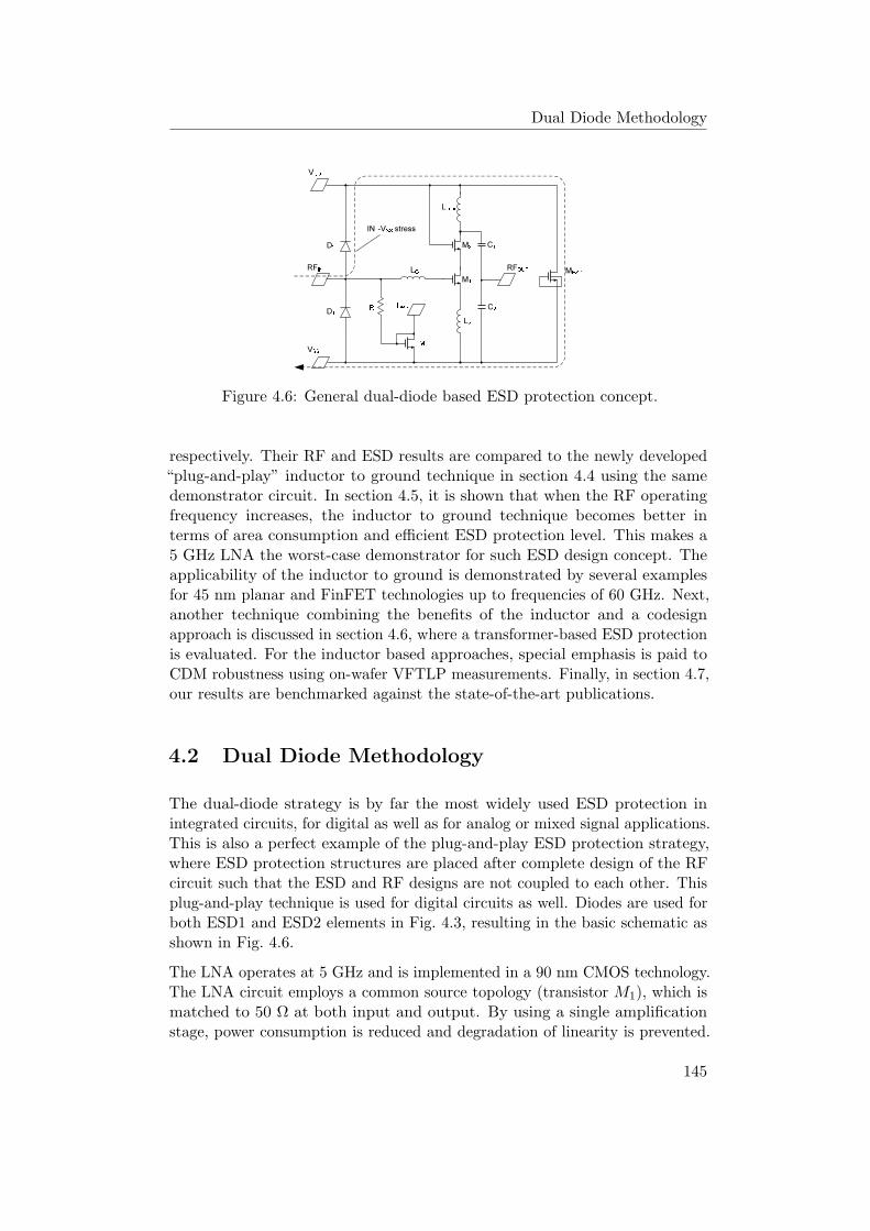
Dual Diode Methodology
LSLG
M1M2LLoad
C2RFIN RFOUTC1VDD
VSSR M3IBIAS MESD
D1D2 IN+-VSS stress
Figure 4.6: General dual-diode based ESD protection concept.
respectively. Their RF and ESD results are compared to the newly developed“plug-and-play” inductor to ground technique in section 4.4 using the samedemonstrator circuit. In section 4.5, it is shown that when the RF operatingfrequency increases, the inductor to ground technique becomes better interms of area consumption and efficient ESD protection level. This makes a5 GHz LNA the worst-case demonstrator for such ESD design concept. Theapplicability of the inductor to ground is demonstrated by several examplesfor 45 nm planar and FinFET technologies up to frequencies of 60 GHz. Next,another technique combining the benefits of the inductor and a codesignapproach is discussed in section 4.6, where a transformer-based ESD protectionis evaluated. For the inductor based approaches, special emphasis is paid toCDM robustness using on-wafer VFTLP measurements. Finally, in section 4.7,our results are benchmarked against the state-of-the-art publications.
4.2 Dual Diode Methodology
The dual-diode strategy is by far the most widely used ESD protection inintegrated circuits, for digital as well as for analog or mixed signal applications.This is also a perfect example of the plug-and-play ESD protection strategy,where ESD protection structures are placed after complete design of the RFcircuit such that the ESD and RF designs are not coupled to each other. Thisplug-and-play technique is used for digital circuits as well. Diodes are used forboth ESD1 and ESD2 elements in Fig. 4.3, resulting in the basic schematic asshown in Fig. 4.6.
The LNA operates at 5 GHz and is implemented in a 90 nm CMOS technology.The LNA circuit employs a common source topology (transistor M1), which ismatched to 50 Ω at both input and output. By using a single amplificationstage, power consumption is reduced and degradation of linearity is prevented.
145
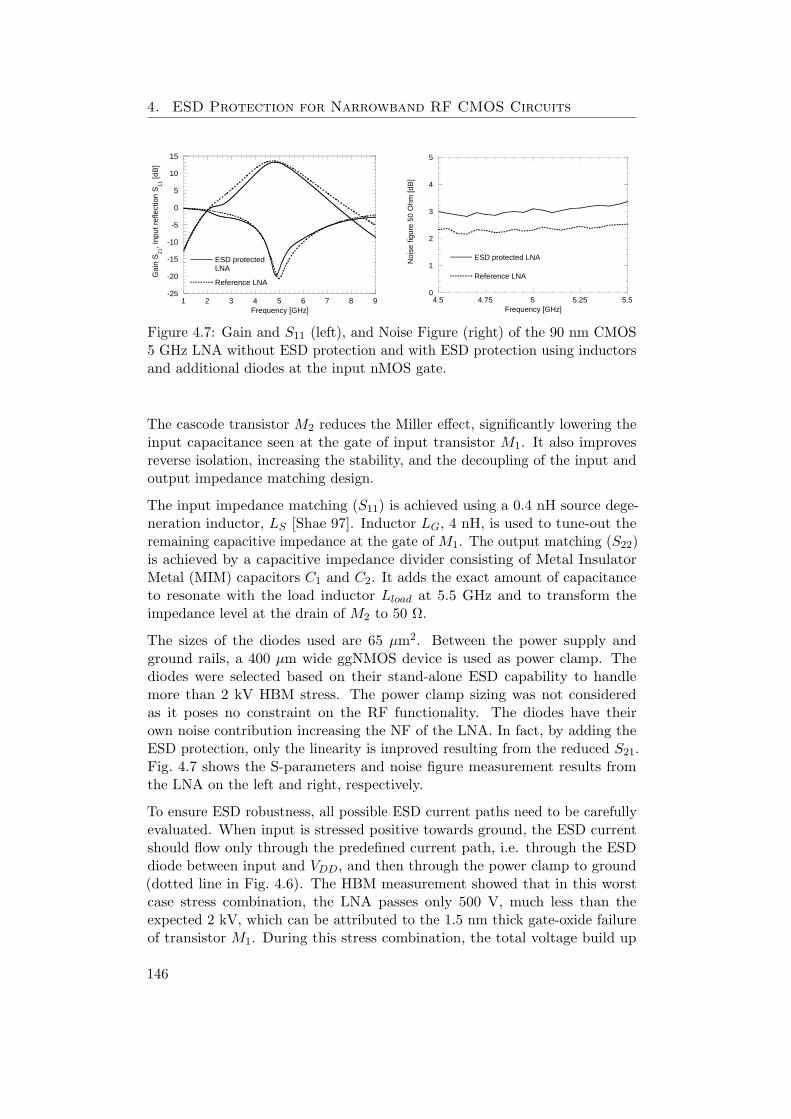
4. ESD Protection for Narrowband RF CMOS Circuits
1 2 3 4 5 6 7 8 9
ESD protectedLNA
Reference LNA
-25
-20
-15
-10
-5
0
5
10
15G
ain
S21
, Inp
ut r
efle
ctio
n S
11 [d
B]
Frequency [GHz]4.5 4.75 5 5.25 5.5
ESD protected LNA
Reference LNA
0
1
2
3
4
5
Noi
se fi
gure
50
Ohm
[dB
]
Frequency [GHz]
Figure 4.7: Gain and S11 (left), and Noise Figure (right) of the 90 nm CMOS5 GHz LNA without ESD protection and with ESD protection using inductorsand additional diodes at the input nMOS gate.
The cascode transistor M2 reduces the Miller effect, significantly lowering theinput capacitance seen at the gate of input transistor M1. It also improvesreverse isolation, increasing the stability, and the decoupling of the input andoutput impedance matching design.
The input impedance matching (S11) is achieved using a 0.4 nH source dege-neration inductor, LS [Shae 97]. Inductor LG, 4 nH, is used to tune-out theremaining capacitive impedance at the gate of M1. The output matching (S22)is achieved by a capacitive impedance divider consisting of Metal InsulatorMetal (MIM) capacitors C1 and C2. It adds the exact amount of capacitanceto resonate with the load inductor Lload at 5.5 GHz and to transform theimpedance level at the drain of M2 to 50 Ω.
The sizes of the diodes used are 65 µm2. Between the power supply andground rails, a 400 µm wide ggNMOS device is used as power clamp. Thediodes were selected based on their stand-alone ESD capability to handlemore than 2 kV HBM stress. The power clamp sizing was not consideredas it poses no constraint on the RF functionality. The diodes have theirown noise contribution increasing the NF of the LNA. In fact, by adding theESD protection, only the linearity is improved resulting from the reduced S21.Fig. 4.7 shows the S-parameters and noise figure measurement results fromthe LNA on the left and right, respectively.
To ensure ESD robustness, all possible ESD current paths need to be carefullyevaluated. When input is stressed positive towards ground, the ESD currentshould flow only through the predefined current path, i.e. through the ESDdiode between input and VDD, and then through the power clamp to ground(dotted line in Fig. 4.6). The HBM measurement showed that in this worstcase stress combination, the LNA passes only 500 V, much less than theexpected 2 kV, which can be attributed to the 1.5 nm thick gate-oxide failureof transistor M1. During this stress combination, the total voltage build up
146
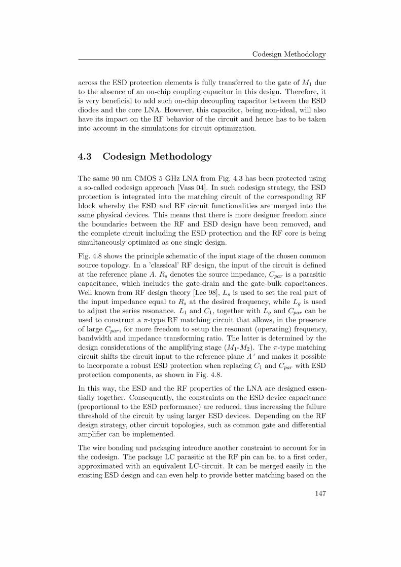
Codesign Methodology
across the ESD protection elements is fully transferred to the gate of M1 dueto the absence of an on-chip coupling capacitor in this design. Therefore, itis very beneficial to add such on-chip decoupling capacitor between the ESDdiodes and the core LNA. However, this capacitor, being non-ideal, will alsohave its impact on the RF behavior of the circuit and hence has to be takeninto account in the simulations for circuit optimization.
4.3 Codesign Methodology
The same 90 nm CMOS 5 GHz LNA from Fig. 4.3 has been protected usinga so-called codesign approach [Vass 04]. In such codesign strategy, the ESDprotection is integrated into the matching circuit of the corresponding RFblock whereby the ESD and RF circuit functionalities are merged into thesame physical devices. This means that there is more designer freedom sincethe boundaries between the RF and ESD design have been removed, andthe complete circuit including the ESD protection and the RF core is beingsimultaneously optimized as one single design.
Fig. 4.8 shows the principle schematic of the input stage of the chosen commonsource topology. In a ’classical’ RF design, the input of the circuit is definedat the reference plane A. Rs denotes the source impedance, Cpar is a parasiticcapacitance, which includes the gate-drain and the gate-bulk capacitances.Well known from RF design theory [Lee 98], Ls is used to set the real part ofthe input impedance equal to Rs at the desired frequency, while Lg is usedto adjust the series resonance. L1 and C1, together with Lg and Cpar can beused to construct a π-type RF matching circuit that allows, in the presenceof large Cpar, for more freedom to setup the resonant (operating) frequency,bandwidth and impedance transforming ratio. The latter is determined by thedesign considerations of the amplifying stage (M1-M2). The π-type matchingcircuit shifts the circuit input to the reference plane A’ and makes it possibleto incorporate a robust ESD protection when replacing C1 and Cpar with ESDprotection components, as shown in Fig. 4.8.
In this way, the ESD and the RF properties of the LNA are designed essen-tially together. Consequently, the constraints on the ESD device capacitance(proportional to the ESD performance) are reduced, thus increasing the failurethreshold of the circuit by using larger ESD devices. Depending on the RFdesign strategy, other circuit topologies, such as common gate and differentialamplifier can be implemented.
The wire bonding and packaging introduce another constraint to account for inthe codesign. The package LC parasitic at the RF pin can be, to a first order,approximated with an equivalent LC-circuit. It can be merged easily in theexisting ESD design and can even help to provide better matching based on the
147
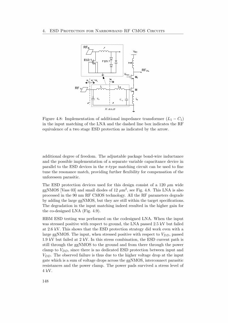
4. ESD Protection for Narrowband RF CMOS Circuits
LsM1M2Lload
-match CparC1eqA
RRS Rin'=RSA'
Z VDDL1 LGRFIN
RFINRFOUTESD 1 ESD 2 VBias
Figure 4.8: Implementation of additional impedance transformer (L1 − C1)in the input matching of the LNA and the dashed line box indicates the RFequivalence of a two stage ESD protection as indicated by the arrow.
additional degree of freedom. The adjustable package bond-wire inductanceand the possible implementation of a separate variable capacitance device inparallel to the ESD devices in the π-type matching circuit can be used to finetune the resonance match, providing further flexibility for compensation of theunforeseen parasitic.
The ESD protection devices used for this design consist of a 120 µm wideggNMOS [Vass 03] and small diodes of 12 µm2, see Fig. 4.8. This LNA is alsoprocessed in the 90 nm RF CMOS technology. All the RF parameters degradeby adding the large ggNMOS, but they are still within the target specifications.The degradation in the input matching indeed resulted in the higher gain forthe co-designed LNA (Fig. 4.9).
HBM ESD testing was performed on the codesigned LNA. When the inputwas stressed positive with respect to ground, the LNA passed 2.5 kV but failedat 2.6 kV. This shows that the ESD protection strategy did work even with alarge ggNMOS. The input, when stressed positive with respect to VDD, passed1.9 kV but failed at 2 kV. In this stress combination, the ESD current path isstill through the ggNMOS to the ground and from there through the powerclamp to VDD, since there is no dedicated ESD protection between input andVDD. The observed failure is thus due to the higher voltage drop at the inputgate which is a sum of voltage drops across the ggNMOS, interconnect parasiticresistances and the power clamp. The power pads survived a stress level of4 kV.
148
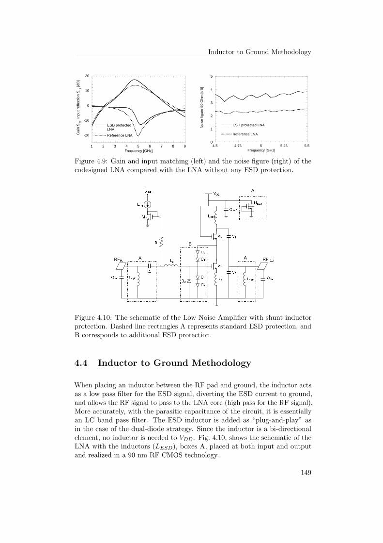
Inductor to Ground Methodology
1 2 3 4 5 6 7 8 9
ESD protectedLNA
Reference LNA-20
-10
0
10
20G
ain
S21
, Inp
ut r
efle
ctio
n S
11 [d
B]
Frequency [GHz]4.5 4.75 5 5.25 5.5
ESD protected LNA
Reference LNA
0
1
2
3
4
5
Noi
se fi
gure
50
Ohm
[dB
]
Frequency [GHz]
Figure 4.9: Gain and input matching (left) and the noise figure (right) of thecodesigned LNA compared with the LNA without any ESD protection.
RCc LsLg M1
M2LloadVDD
C2RFIN RFOUTLESD LESDCpadC1
MESD
Cpad
CDEC
D3 D2D1D5D4
M1'IBIASA
A
A
B
bias
Figure 4.10: The schematic of the Low Noise Amplifier with shunt inductorprotection. Dashed line rectangles A represents standard ESD protection, andB corresponds to additional ESD protection.
4.4 Inductor to Ground Methodology
When placing an inductor between the RF pad and ground, the inductor actsas a low pass filter for the ESD signal, diverting the ESD current to ground,and allows the RF signal to pass to the LNA core (high pass for the RF signal).More accurately, with the parasitic capacitance of the circuit, it is essentiallyan LC band pass filter. The ESD inductor is added as “plug-and-play” asin the case of the dual-diode strategy. Since the inductor is a bi-directionalelement, no inductor is needed to VDD. Fig. 4.10, shows the schematic of theLNA with the inductors (LESD), boxes A, placed at both input and outputand realized in a 90 nm RF CMOS technology.
149
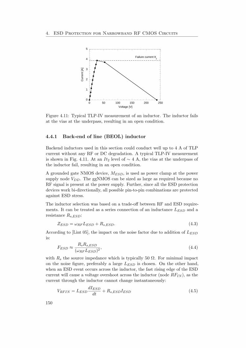
4. ESD Protection for Narrowband RF CMOS Circuits
0
1
2
3
4
5
0 50 100 150 200 250
Cur
rent
[A]
Voltage [V]
Failure current It2
Figure 4.11: Typical TLP-IV measurement of an inductor. The inductor failsat the vias at the underpass, resulting in an open condition.
4.4.1 Back-end of line (BEOL) inductor
Backend inductors used in this section could conduct well up to 4 A of TLPcurrent without any RF or DC degradation. A typical TLP-IV measurementis shown in Fig. 4.11. At an It2 level of ∼ 4 A, the vias at the underpass ofthe inductor fail, resulting in an open condition.
A grounded gate NMOS device, MESD, is used as power clamp at the powersupply node VDD. The ggNMOS can be sized as large as required because noRF signal is present at the power supply. Further, since all the ESD protectiondevices work bi-directionally, all possible pin-to-pin combinations are protectedagainst ESD stress.
The inductor selection was based on a trade-off between RF and ESD require-ments. It can be treated as a series connection of an inductance LESD and aresistance Rs,ESD:
ZESD = ωRF LESD + Rs,ESD. (4.3)
According to [Lint 05], the impact on the noise factor due to addition of LESD
is:
FESD ≈RsRs,ESD
(ωRF LESD)2, (4.4)
with Rs the source impedance which is typically 50 Ω. For minimal impacton the noise figure, preferably a large LESD is chosen. On the other hand,when an ESD event occurs across the inductor, the fast rising edge of the ESDcurrent will cause a voltage overshoot across the inductor (node RFIN ), as thecurrent through the inductor cannot change instantaneously:
VRFIN = LESDdIESD
dt+ Rs,ESDIESD (4.5)
150
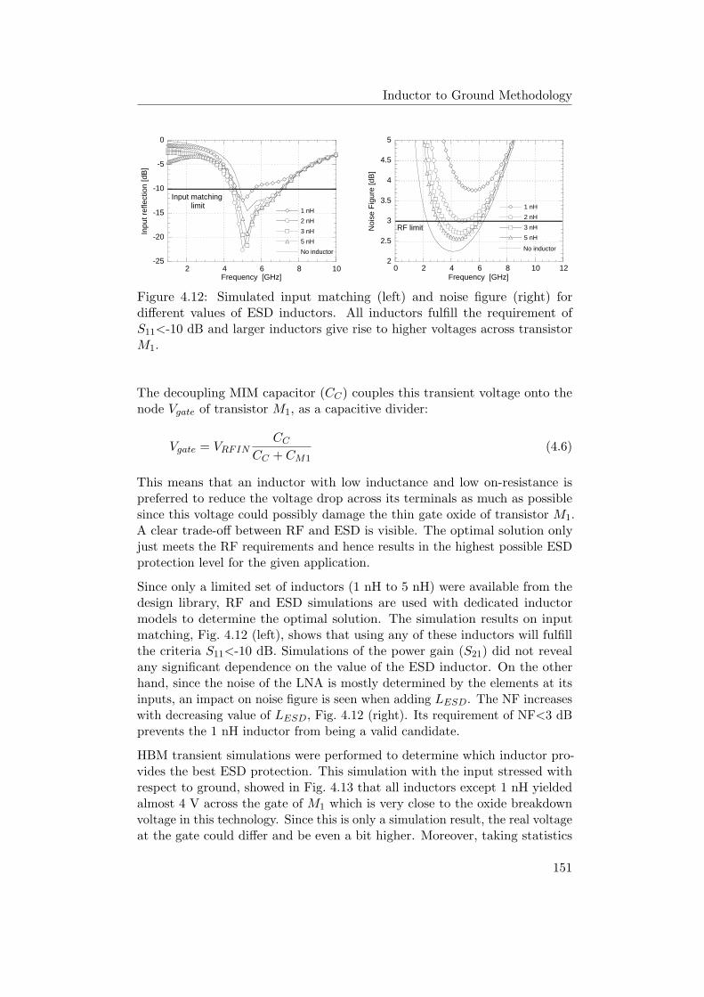
Inductor to Ground Methodology
-25
-20
-15
-10
-5
0
2 4 6 8 10
No inductor
1 nH
2 nH
3 nH
5 nH
Inpu
t ref
lect
ion
[dB
]
Frequency [GHz]
Input matching limit
2
2.5
3
3.5
4
4.5
5
0 2 4 6 8 10 12
No inductor
1 nH
2 nH
3 nH
5 nH
Noi
se F
igur
e [d
B]
Frequency [GHz]
RF limit
Figure 4.12: Simulated input matching (left) and noise figure (right) fordifferent values of ESD inductors. All inductors fulfill the requirement ofS11<-10 dB and larger inductors give rise to higher voltages across transistorM1.
The decoupling MIM capacitor (CC) couples this transient voltage onto thenode Vgate of transistor M1, as a capacitive divider:
Vgate = VRFINCC
CC + CM1(4.6)
This means that an inductor with low inductance and low on-resistance ispreferred to reduce the voltage drop across its terminals as much as possiblesince this voltage could possibly damage the thin gate oxide of transistor M1.A clear trade-off between RF and ESD is visible. The optimal solution onlyjust meets the RF requirements and hence results in the highest possible ESDprotection level for the given application.
Since only a limited set of inductors (1 nH to 5 nH) were available from thedesign library, RF and ESD simulations are used with dedicated inductormodels to determine the optimal solution. The simulation results on inputmatching, Fig. 4.12 (left), shows that using any of these inductors will fulfillthe criteria S11<-10 dB. Simulations of the power gain (S21) did not revealany significant dependence on the value of the ESD inductor. On the otherhand, since the noise of the LNA is mostly determined by the elements at itsinputs, an impact on noise figure is seen when adding LESD. The NF increaseswith decreasing value of LESD, Fig. 4.12 (right). Its requirement of NF<3 dBprevents the 1 nH inductor from being a valid candidate.
HBM transient simulations were performed to determine which inductor pro-vides the best ESD protection. This simulation with the input stressed withrespect to ground, showed in Fig. 4.13 that all inductors except 1 nH yieldedalmost 4 V across the gate of M1 which is very close to the oxide breakdownvoltage in this technology. Since this is only a simulation result, the real voltageat the gate could differ and be even a bit higher. Moreover, taking statistics
151
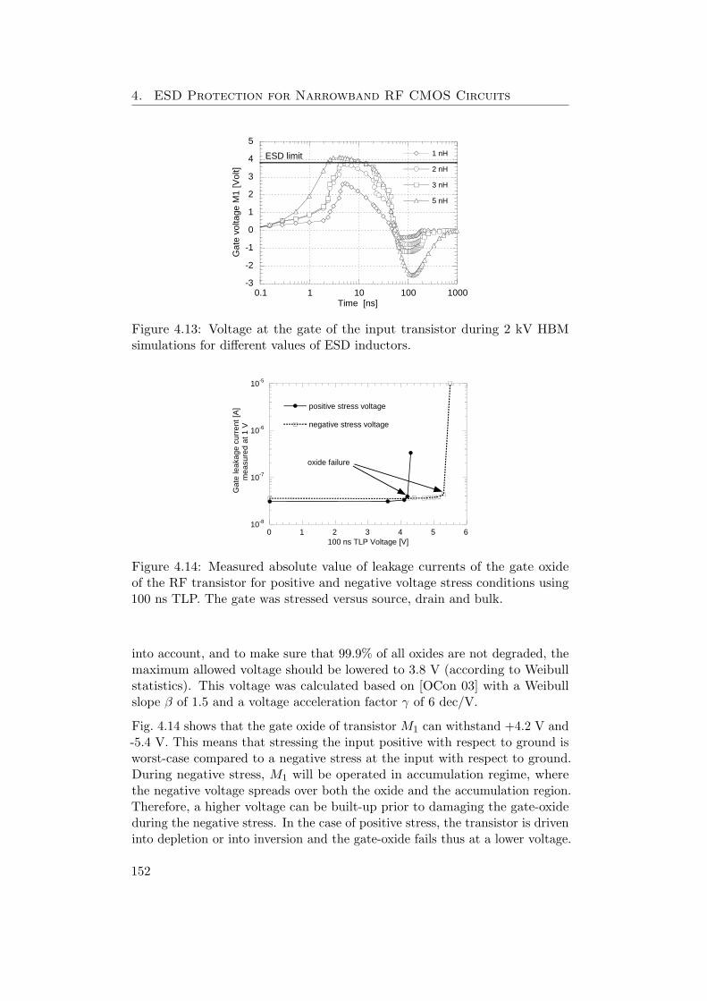
4. ESD Protection for Narrowband RF CMOS Circuits
-3
-2
-1
0
1
2
3
4
5
0.1 1 10 100 1000
1 nH
2 nH
3 nH
5 nH
Gat
e vo
ltage
M1
[Vol
t]
Time [ns]
ESD limit
Figure 4.13: Voltage at the gate of the input transistor during 2 kV HBMsimulations for different values of ESD inductors.
0 1 2 3 4 5 6
positive stress voltage
negative stress voltage
10-8
10-7
10-6
10-5
Gat
e le
akag
e cu
rren
t [A
]m
easu
red
at 1
V
100 ns TLP Voltage [V]
oxide failure
Figure 4.14: Measured absolute value of leakage currents of the gate oxideof the RF transistor for positive and negative voltage stress conditions using100 ns TLP. The gate was stressed versus source, drain and bulk.
into account, and to make sure that 99.9% of all oxides are not degraded, themaximum allowed voltage should be lowered to 3.8 V (according to Weibullstatistics). This voltage was calculated based on [OCon 03] with a Weibullslope β of 1.5 and a voltage acceleration factor γ of 6 dec/V.
Fig. 4.14 shows that the gate oxide of transistor M1 can withstand +4.2 V and-5.4 V. This means that stressing the input positive with respect to ground isworst-case compared to a negative stress at the input with respect to ground.During negative stress, M1 will be operated in accumulation regime, wherethe negative voltage spreads over both the oxide and the accumulation region.Therefore, a higher voltage can be built-up prior to damaging the gate-oxideduring the negative stress. In the case of positive stress, the transistor is driveninto depletion or into inversion and the gate-oxide fails thus at a lower voltage.
152
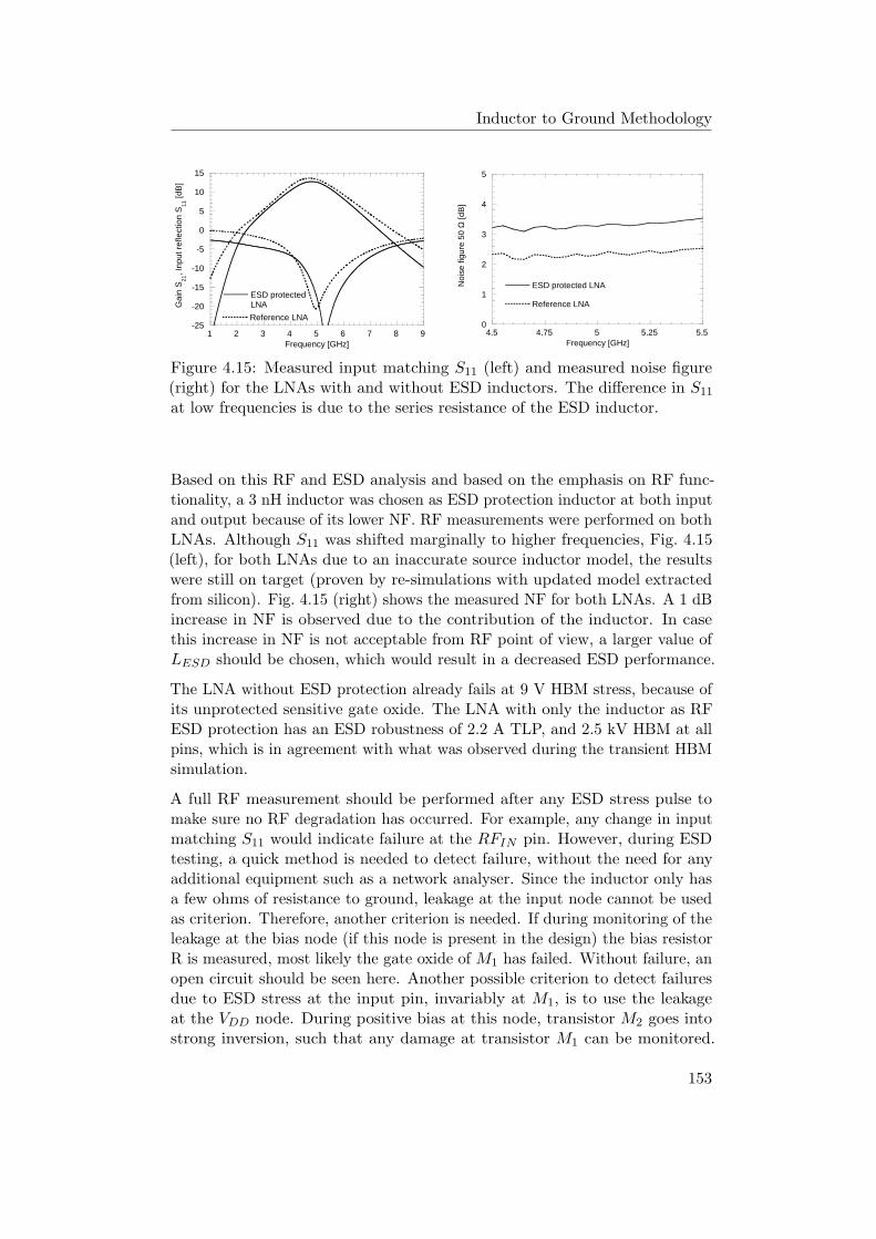
Inductor to Ground Methodology
1 2 3 4 5 6 7 8 9
ESD protectedLNA
Reference LNA-25
-20
-15
-10
-5
0
5
10
15G
ain
S21
, Inp
ut r
efle
ctio
n S
11 [d
B]
Frequency [GHz]4.5 4.75 5 5.25 5.5
ESD protected LNA
Reference LNA
0
1
2
3
4
5
Noi
se fi
gure
50
Ω [d
B]
Frequency [GHz]
Figure 4.15: Measured input matching S11 (left) and measured noise figure(right) for the LNAs with and without ESD inductors. The difference in S11
at low frequencies is due to the series resistance of the ESD inductor.
Based on this RF and ESD analysis and based on the emphasis on RF func-tionality, a 3 nH inductor was chosen as ESD protection inductor at both inputand output because of its lower NF. RF measurements were performed on bothLNAs. Although S11 was shifted marginally to higher frequencies, Fig. 4.15(left), for both LNAs due to an inaccurate source inductor model, the resultswere still on target (proven by re-simulations with updated model extractedfrom silicon). Fig. 4.15 (right) shows the measured NF for both LNAs. A 1 dBincrease in NF is observed due to the contribution of the inductor. In casethis increase in NF is not acceptable from RF point of view, a larger value ofLESD should be chosen, which would result in a decreased ESD performance.
The LNA without ESD protection already fails at 9 V HBM stress, because ofits unprotected sensitive gate oxide. The LNA with only the inductor as RFESD protection has an ESD robustness of 2.2 A TLP, and 2.5 kV HBM at allpins, which is in agreement with what was observed during the transient HBMsimulation.
A full RF measurement should be performed after any ESD stress pulse tomake sure no RF degradation has occurred. For example, any change in inputmatching S11 would indicate failure at the RFIN pin. However, during ESDtesting, a quick method is needed to detect failure, without the need for anyadditional equipment such as a network analyser. Since the inductor only hasa few ohms of resistance to ground, leakage at the input node cannot be usedas criterion. Therefore, another criterion is needed. If during monitoring of theleakage at the bias node (if this node is present in the design) the bias resistorR is measured, most likely the gate oxide of M1 has failed. Without failure, anopen circuit should be seen here. Another possible criterion to detect failuresdue to ESD stress at the input pin, invariably at M1, is to use the leakageat the VDD node. During positive bias at this node, transistor M2 goes intostrong inversion, such that any damage at transistor M1 can be monitored.
153
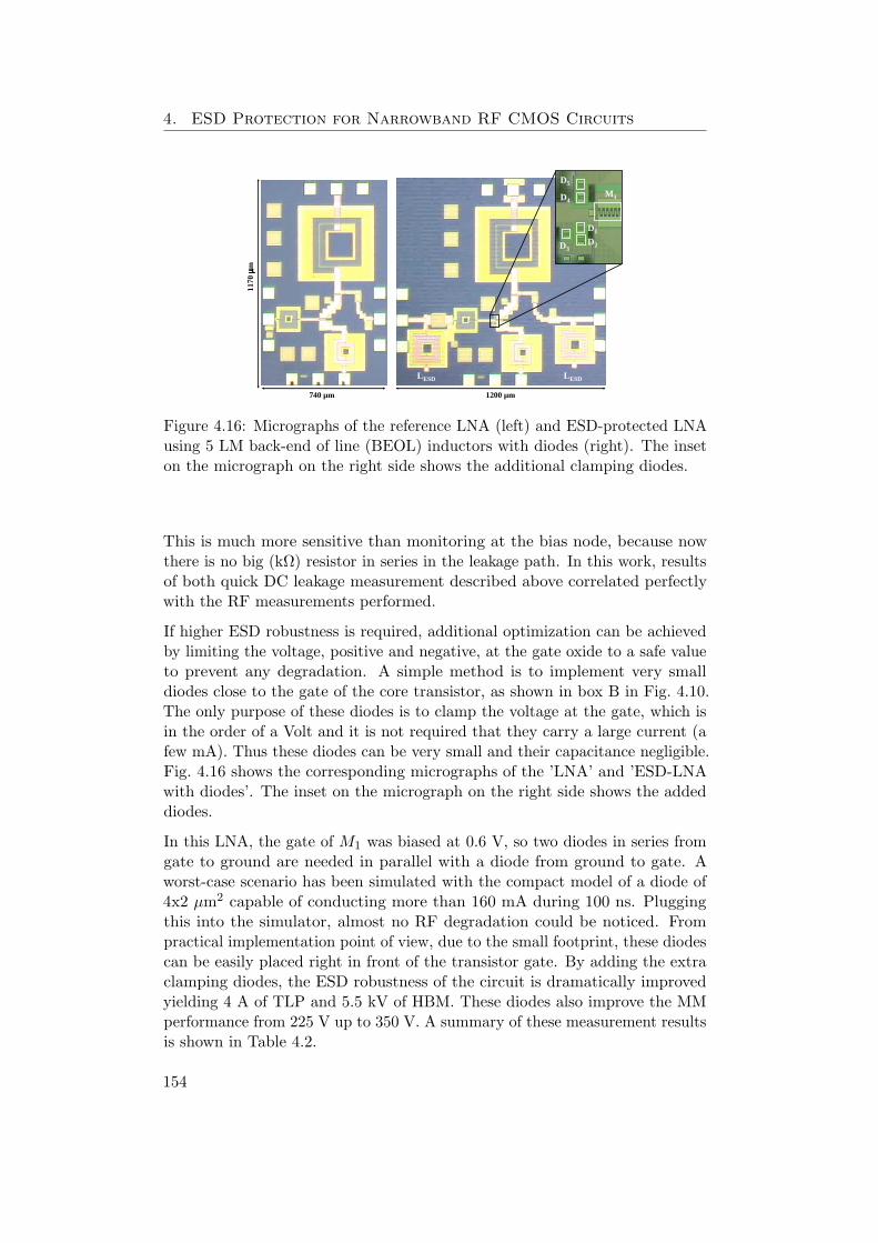
4. ESD Protection for Narrowband RF CMOS Circuits
1200 µm740 µm
LESD
1170
µµ µµm
LESD
D1
D5
M 1
D3D2
D4
Figure 4.16: Micrographs of the reference LNA (left) and ESD-protected LNAusing 5 LM back-end of line (BEOL) inductors with diodes (right). The inseton the micrograph on the right side shows the additional clamping diodes.
This is much more sensitive than monitoring at the bias node, because nowthere is no big (kΩ) resistor in series in the leakage path. In this work, resultsof both quick DC leakage measurement described above correlated perfectlywith the RF measurements performed.
If higher ESD robustness is required, additional optimization can be achievedby limiting the voltage, positive and negative, at the gate oxide to a safe valueto prevent any degradation. A simple method is to implement very smalldiodes close to the gate of the core transistor, as shown in box B in Fig. 4.10.The only purpose of these diodes is to clamp the voltage at the gate, which isin the order of a Volt and it is not required that they carry a large current (afew mA). Thus these diodes can be very small and their capacitance negligible.Fig. 4.16 shows the corresponding micrographs of the ’LNA’ and ’ESD-LNAwith diodes’. The inset on the micrograph on the right side shows the addeddiodes.
In this LNA, the gate of M1 was biased at 0.6 V, so two diodes in series fromgate to ground are needed in parallel with a diode from ground to gate. Aworst-case scenario has been simulated with the compact model of a diode of4x2 µm2 capable of conducting more than 160 mA during 100 ns. Pluggingthis into the simulator, almost no RF degradation could be noticed. Frompractical implementation point of view, due to the small footprint, these diodescan be easily placed right in front of the transistor gate. By adding the extraclamping diodes, the ESD robustness of the circuit is dramatically improvedyielding 4 A of TLP and 5.5 kV of HBM. These diodes also improve the MMperformance from 225 V up to 350 V. A summary of these measurement resultsis shown in Table 4.2.
154
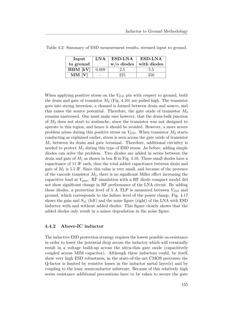
Inductor to Ground Methodology
Table 4.2: Summary of ESD measurement results, stressed input to ground.
Input LNA ESD-LNA ESD-LNAto ground w/o diodes with diodesHBM [kV] 0.009 2.5 5.5MM [V] - 225 350
When applying positive stress on the VDD pin with respect to ground, boththe drain and gate of transistor M2 (Fig. 4.10) are pulled high. The transistorgoes into strong inversion, a channel is formed between drain and source, andthis raises the source potential. Therefore, the gate oxide of transistor M2
remains unstressed. One must make sure however, that the drain-bulk junctionof M2 does not start to avalanche, since the transistor was not designed tooperate in this region, and hence it should be avoided. However, a more severeproblem arises during this positive stress on VDD. When transistor M2 startsconducting as explained earlier, stress is seen across the gate oxide of transistorM1 between its drain and gate terminal. Therefore, additional circuitry isneeded to protect M1 during this type of ESD stress. As before, adding simplediodes can solve the problem. Two diodes are added in series between thedrain and gate of M1 as shown in box B in Fig. 4.10. These small diodes have acapacitance of 11 fF each, thus the total added capacitance between drain andgate of M1 is 5.5 fF. Since this value is very small, and because of the presenceof the cascode transistor M2, there is no significant Miller effect increasing thecapacitive load at Vgate. RF simulation with a RF diode compact model didnot show significant change in RF performance of the LNA circuit. By addingthese diodes, a protection level of 5 A TLP is measured between VDD andground, which corresponds to the failure level of the power clamp. Fig. 4.17shows the gain and S11 (left) and the noise figure (right) of the LNA with ESDinductor with and without added diodes. This figure clearly shows that theadded diodes only result in a minor degradation in the noise figure.
4.4.2 Above-IC inductor
The inductive ESD protection strategy requires the lowest possible on-resistancein order to lower the potential drop across the inductor which will eventuallyresult in a voltage build-up across the ultra-thin gate oxide (capacitivelycoupled across MIM capacitor). Although these inductors could, by itself,show very high ESD robustness, in the state-of-the-art CMOS processes theQ-factor is limited by resistive losses in the inductor metal layer(s) and bycoupling to the lossy semiconductor substrate. Because of this relatively highseries resistance additional precautions have to be taken to secure the gate
155
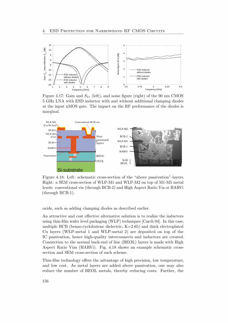
4. ESD Protection for Narrowband RF CMOS Circuits
1 2 3 4 5 6 7 8 9
ESD inductorwithout diodesESD inductorwith diodes
-25
-20
-15
-10
-5
0
5
10
15G
ain
S21
, Inp
ut r
efle
ctio
n S
11 [d
B]
Frequency [GHz]4.5 4.75 5 5.25 5.5
ESD inductorwithout diodes
ESD inductorwith diodes
0
1
2
3
4
5
Noi
se fi
gure
50
Ω [d
B]
Frequency [GHz]
Figure 4.17: Gain and S11 (left), and noise figure (right) of the 90 nm CMOS5 GHz LNA with ESD inductor with and without additional clamping diodesat the input nMOS gate. The impact on the RF performance of the diodes ismarginal.
Si-substrate
BEOL
Post-processedlayers
(Cu)
BCB-2
BCB-1
WLP-M2
FEOL
HARVi
(Cu/Ni/Au)
Passivation
Conventional BCB-via
WLP-M1
5LM BEOL
HARVi
BCB-1
BCB-2
WLP-M2
WLP-M1
Figure 4.18: Left: schematic cross-section of the “above passivation”-layers.Right: a SEM cross-section of WLP-M1 and WLP-M2 on top of M1-M5 metallevels: conventional via (through BCB-2) and High Aspect Ratio Via or HARVi(through BCB-1).
oxide, such as adding clamping diodes as described earlier.
An attractive and cost effective alternative solution is to realize the inductorsusing thin-film wafer level packaging (WLP) techniques [Carch 04]. In this case,multiple BCB (benzo-cyclobutene dielectric, K=2.65) and thick electroplatedCu layers (WLP-metal 1 and WLP-metal 2) are deposited on top of theIC passivation, hence high-quality interconnects and inductors are created.Connection to the normal back-end of line (BEOL) layers is made with HighAspect Ratio Vias (HARVi). Fig. 4.18 shows an example schematic cross-section and SEM cross-section of such scheme.
Thin-film technology offers the advantage of high precision, low temperature,and low cost. As metal layers are added above passivation, one may alsoreduce the number of BEOL metals, thereby reducing costs. Further, the
156
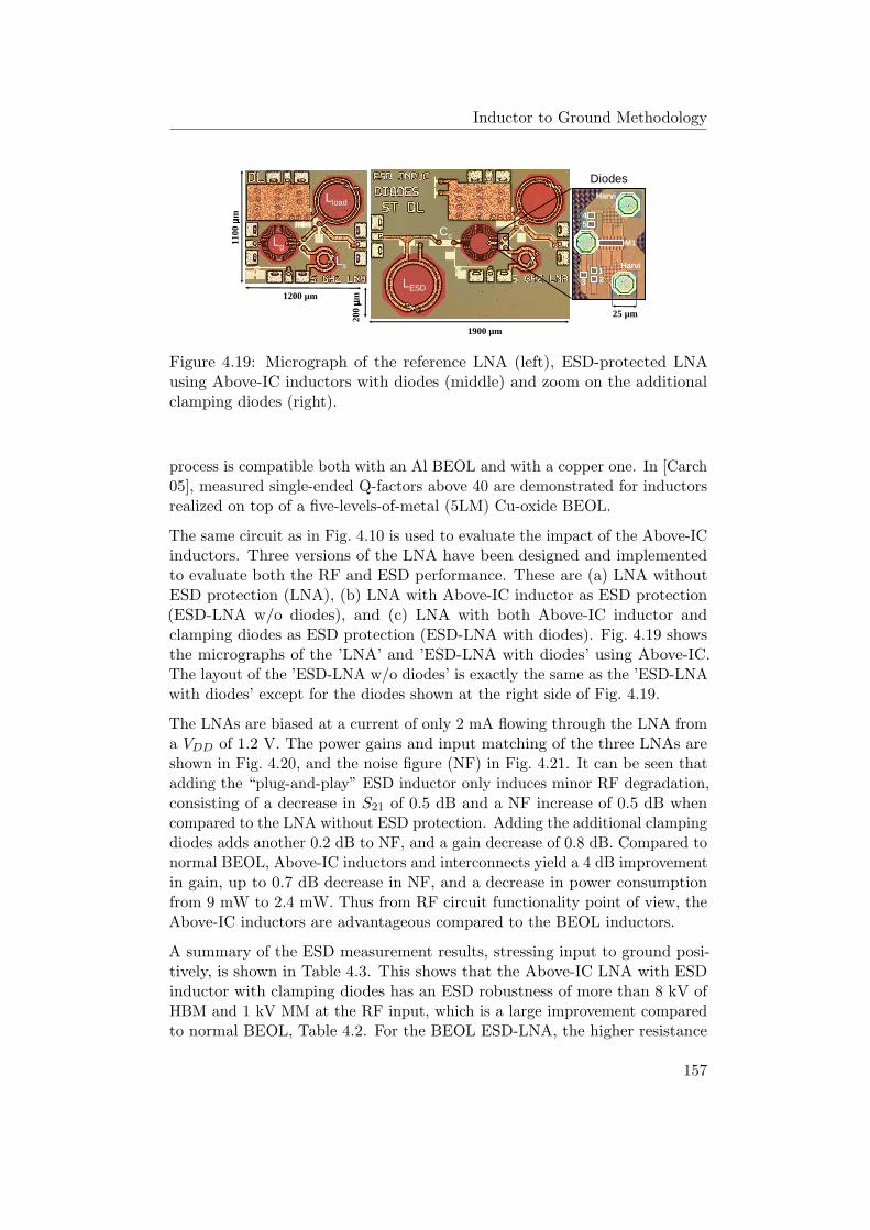
Inductor to Ground Methodology
1900 µm
200
µµ µµm
1100
µµ µµm
1200 µm
Lload
Lg
Ls
LESD
Cc
Diodes
54
123
Harvi
M1
Harvi
25 µm
Figure 4.19: Micrograph of the reference LNA (left), ESD-protected LNAusing Above-IC inductors with diodes (middle) and zoom on the additionalclamping diodes (right).
process is compatible both with an Al BEOL and with a copper one. In [Carch05], measured single-ended Q-factors above 40 are demonstrated for inductorsrealized on top of a five-levels-of-metal (5LM) Cu-oxide BEOL.
The same circuit as in Fig. 4.10 is used to evaluate the impact of the Above-ICinductors. Three versions of the LNA have been designed and implementedto evaluate both the RF and ESD performance. These are (a) LNA withoutESD protection (LNA), (b) LNA with Above-IC inductor as ESD protection(ESD-LNA w/o diodes), and (c) LNA with both Above-IC inductor andclamping diodes as ESD protection (ESD-LNA with diodes). Fig. 4.19 showsthe micrographs of the ’LNA’ and ’ESD-LNA with diodes’ using Above-IC.The layout of the ’ESD-LNA w/o diodes’ is exactly the same as the ’ESD-LNAwith diodes’ except for the diodes shown at the right side of Fig. 4.19.
The LNAs are biased at a current of only 2 mA flowing through the LNA froma VDD of 1.2 V. The power gains and input matching of the three LNAs areshown in Fig. 4.20, and the noise figure (NF) in Fig. 4.21. It can be seen thatadding the “plug-and-play” ESD inductor only induces minor RF degradation,consisting of a decrease in S21 of 0.5 dB and a NF increase of 0.5 dB whencompared to the LNA without ESD protection. Adding the additional clampingdiodes adds another 0.2 dB to NF, and a gain decrease of 0.8 dB. Compared tonormal BEOL, Above-IC inductors and interconnects yield a 4 dB improvementin gain, up to 0.7 dB decrease in NF, and a decrease in power consumptionfrom 9 mW to 2.4 mW. Thus from RF circuit functionality point of view, theAbove-IC inductors are advantageous compared to the BEOL inductors.
A summary of the ESD measurement results, stressing input to ground posi-tively, is shown in Table 4.3. This shows that the Above-IC LNA with ESDinductor with clamping diodes has an ESD robustness of more than 8 kV ofHBM and 1 kV MM at the RF input, which is a large improvement comparedto normal BEOL, Table 4.2. For the BEOL ESD-LNA, the higher resistance
157
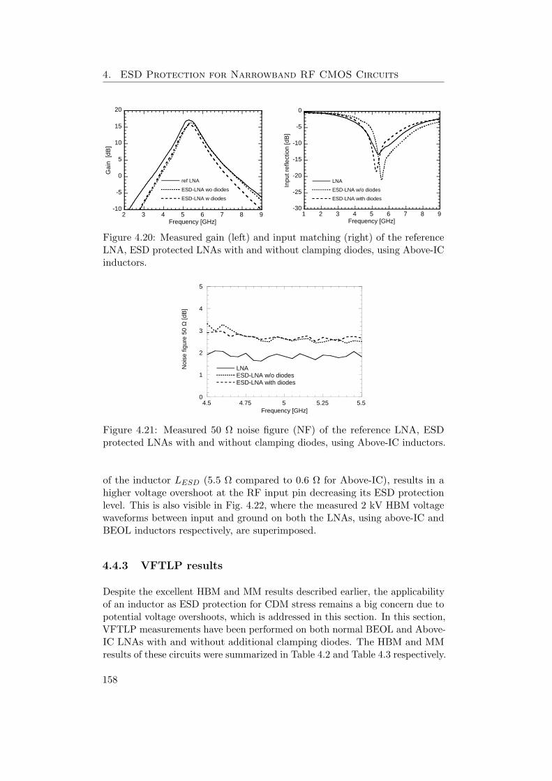
4. ESD Protection for Narrowband RF CMOS Circuits
-10
-5
0
5
10
15
20
2 3 4 5 6 7 8 9
ref LNA
ESD-LNA wo diodes
ESD-LNA w diodes
Gai
n [d
B]
Frequency [GHz]
-30
-25
-20
-15
-10
-5
0
1 2 3 4 5 6 7 8 9
LNA
ESD-LNA w/o diodes
ESD-LNA with diodes
Inpu
t ref
lect
ion
[dB
]
Frequency [GHz]
Figure 4.20: Measured gain (left) and input matching (right) of the referenceLNA, ESD protected LNAs with and without clamping diodes, using Above-ICinductors.
4.5 4.75 5 5.25 5.5
LNAESD-LNA w/o diodesESD-LNA with diodes
0
1
2
3
4
5
Noi
se fi
gure
50
Ω [d
B]
Frequency [GHz]
Figure 4.21: Measured 50 Ω noise figure (NF) of the reference LNA, ESDprotected LNAs with and without clamping diodes, using Above-IC inductors.
of the inductor LESD (5.5 Ω compared to 0.6 Ω for Above-IC), results in ahigher voltage overshoot at the RF input pin decreasing its ESD protectionlevel. This is also visible in Fig. 4.22, where the measured 2 kV HBM voltagewaveforms between input and ground on both the LNAs, using above-IC andBEOL inductors respectively, are superimposed.
4.4.3 VFTLP results
Despite the excellent HBM and MM results described earlier, the applicabilityof an inductor as ESD protection for CDM stress remains a big concern due topotential voltage overshoots, which is addressed in this section. In this section,VFTLP measurements have been performed on both normal BEOL and Above-IC LNAs with and without additional clamping diodes. The HBM and MMresults of these circuits were summarized in Table 4.2 and Table 4.3 respectively.
158
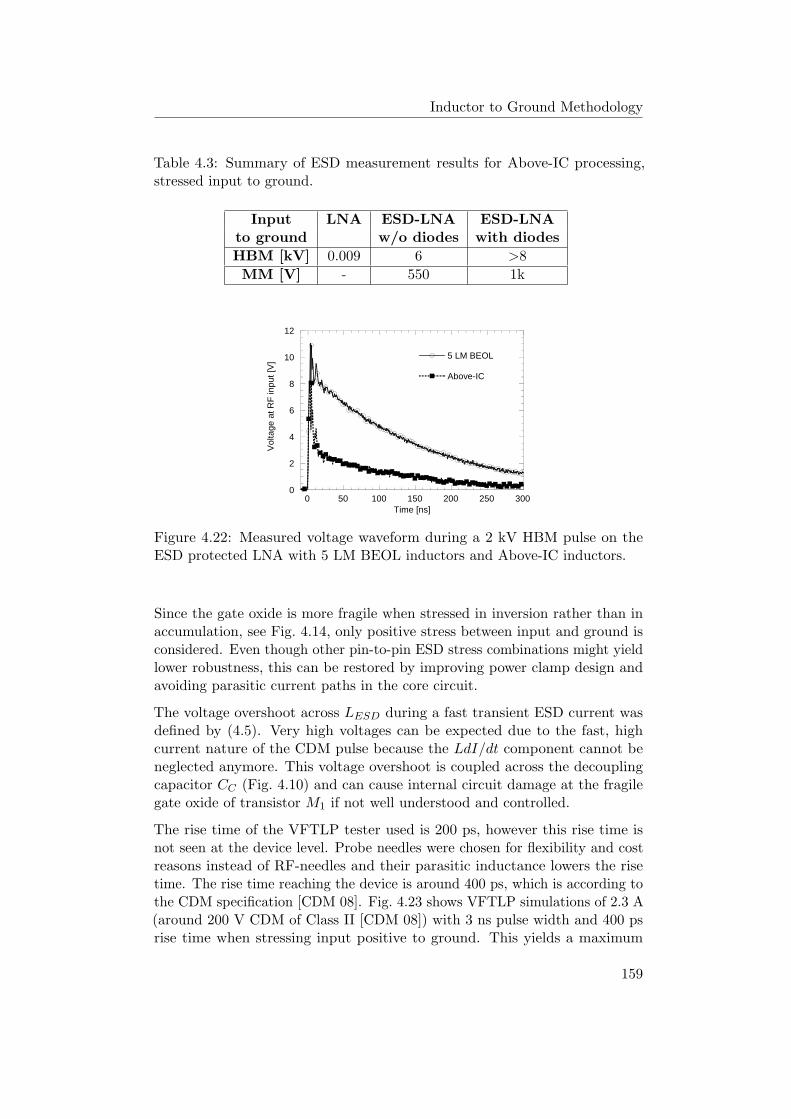
Inductor to Ground Methodology
Table 4.3: Summary of ESD measurement results for Above-IC processing,stressed input to ground.
Input LNA ESD-LNA ESD-LNAto ground w/o diodes with diodesHBM [kV] 0.009 6 >8MM [V] - 550 1k
0 50 100 150 200 250 300
5 LM BEOL
Above-IC
0
2
4
6
8
10
12
Vol
tage
at R
F in
put [
V]
Time [ns]
Figure 4.22: Measured voltage waveform during a 2 kV HBM pulse on theESD protected LNA with 5 LM BEOL inductors and Above-IC inductors.
Since the gate oxide is more fragile when stressed in inversion rather than inaccumulation, see Fig. 4.14, only positive stress between input and ground isconsidered. Even though other pin-to-pin ESD stress combinations might yieldlower robustness, this can be restored by improving power clamp design andavoiding parasitic current paths in the core circuit.
The voltage overshoot across LESD during a fast transient ESD current wasdefined by (4.5). Very high voltages can be expected due to the fast, highcurrent nature of the CDM pulse because the LdI/dt component cannot beneglected anymore. This voltage overshoot is coupled across the decouplingcapacitor CC (Fig. 4.10) and can cause internal circuit damage at the fragilegate oxide of transistor M1 if not well understood and controlled.
The rise time of the VFTLP tester used is 200 ps, however this rise time isnot seen at the device level. Probe needles were chosen for flexibility and costreasons instead of RF-needles and their parasitic inductance lowers the risetime. The rise time reaching the device is around 400 ps, which is according tothe CDM specification [CDM 08]. Fig. 4.23 shows VFTLP simulations of 2.3 A(around 200 V CDM of Class II [CDM 08]) with 3 ns pulse width and 400 psrise time when stressing input positive to ground. This yields a maximum
159
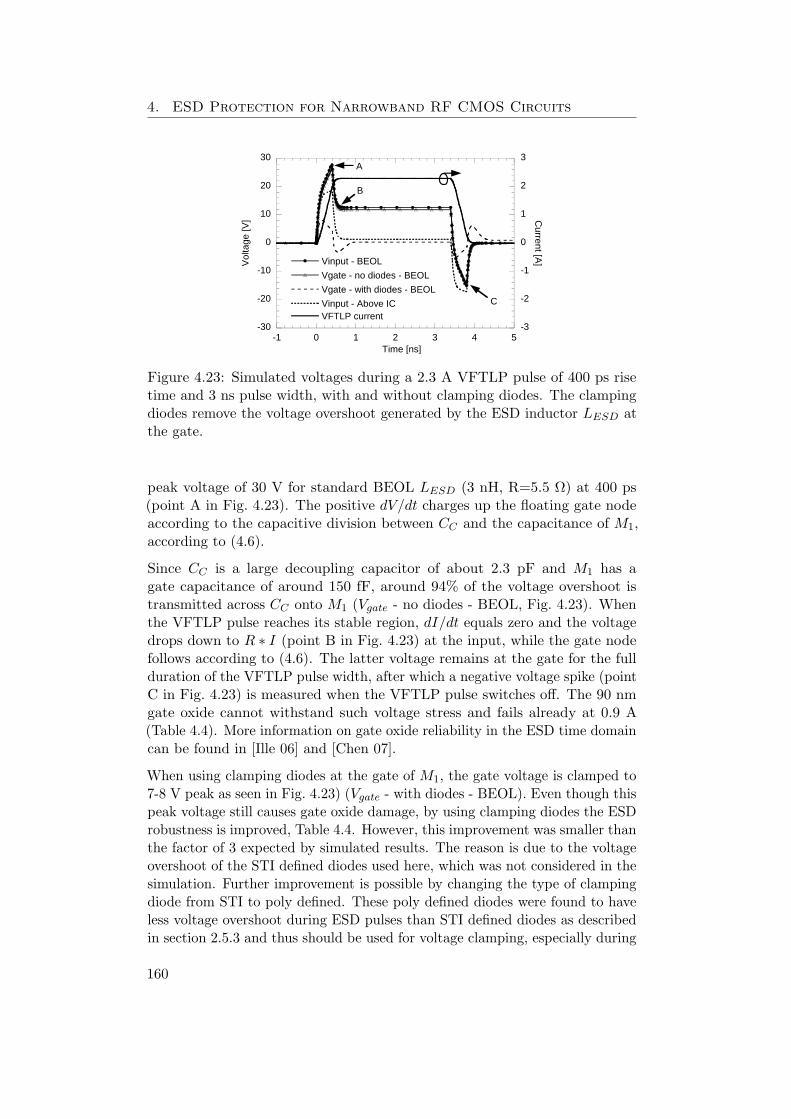
4. ESD Protection for Narrowband RF CMOS Circuits
-30
-20
-10
0
10
20
30
-3
-2
-1
0
1
2
3
-1 0 1 2 3 4 5
Vinput - BEOL
Vgate - no diodes - BEOL
Vgate - with diodes - BEOL
Vinput - Above ICVFTLP current
Vol
tage
[V] C
urrent [A]
Time [ns]
A
B
C
Figure 4.23: Simulated voltages during a 2.3 A VFTLP pulse of 400 ps risetime and 3 ns pulse width, with and without clamping diodes. The clampingdiodes remove the voltage overshoot generated by the ESD inductor LESD atthe gate.
peak voltage of 30 V for standard BEOL LESD (3 nH, R=5.5 Ω) at 400 ps(point A in Fig. 4.23). The positive dV/dt charges up the floating gate nodeaccording to the capacitive division between CC and the capacitance of M1,according to (4.6).
Since CC is a large decoupling capacitor of about 2.3 pF and M1 has agate capacitance of around 150 fF, around 94% of the voltage overshoot istransmitted across CC onto M1 (Vgate - no diodes - BEOL, Fig. 4.23). Whenthe VFTLP pulse reaches its stable region, dI/dt equals zero and the voltagedrops down to R ∗ I (point B in Fig. 4.23) at the input, while the gate nodefollows according to (4.6). The latter voltage remains at the gate for the fullduration of the VFTLP pulse width, after which a negative voltage spike (pointC in Fig. 4.23) is measured when the VFTLP pulse switches off. The 90 nmgate oxide cannot withstand such voltage stress and fails already at 0.9 A(Table 4.4). More information on gate oxide reliability in the ESD time domaincan be found in [Ille 06] and [Chen 07].
When using clamping diodes at the gate of M1, the gate voltage is clamped to7-8 V peak as seen in Fig. 4.23) (Vgate - with diodes - BEOL). Even though thispeak voltage still causes gate oxide damage, by using clamping diodes the ESDrobustness is improved, Table 4.4. However, this improvement was smaller thanthe factor of 3 expected by simulated results. The reason is due to the voltageovershoot of the STI defined diodes used here, which was not considered in thesimulation. Further improvement is possible by changing the type of clampingdiode from STI to poly defined. These poly defined diodes were found to haveless voltage overshoot during ESD pulses than STI defined diodes as describedin section 2.5.3 and thus should be used for voltage clamping, especially during
160
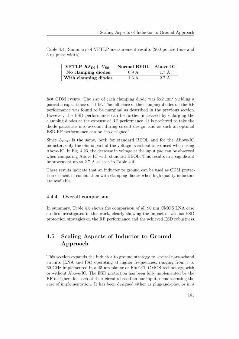
Scaling Aspects of Inductor to Ground Approach
Table 4.4: Summary of VFTLP measurement results (200 ps rise time and3 ns pulse width).
VFTLP RFIN+ VSS- Normal BEOL Above-ICNo clamping diodes 0.9 A 1.7 A
With clamping diodes 1.3 A 2.7 A
fast CDM events. The size of each clamping diode was 5x2 µm2 yielding aparasitic capacitance of 11 fF. The influence of the clamping diodes on the RFperformance was found to be marginal as described in the previous section.However, the ESD performance can be further increased by enlarging theclamping diodes at the expense of RF performance. It is preferred to take thediode parasitics into account during circuit design, and as such an optimalESD-RF performance can be “co-designed”.
Since LESD is the same, both for standard BEOL and for the Above-ICinductor, only the ohmic part of the voltage overshoot is reduced when usingAbove-IC. In Fig. 4.23, the decrease in voltage at the input pad can be observedwhen comparing Above-IC with standard BEOL. This results in a significantimprovement up to 2.7 A as seen in Table 4.4.
These results indicate that an inductor to ground can be used as CDM protec-tion element in combination with clamping diodes when high-quality inductorsare available.
4.4.4 Overall comparison
In summary, Table 4.5 shows the comparison of all 90 nm CMOS LNA casestudies investigated in this work, clearly showing the impact of various ESDprotection strategies on the RF performance and the achieved ESD robustness.
4.5 Scaling Aspects of Inductor to GroundApproach
This section expands the inductor to ground strategy to several narrowbandcircuits (LNA and PA) operating at higher frequencies, ranging from 5 to60 GHz implemented in a 45 nm planar or FinFET CMOS technology, withor without Above-IC. The ESD protection has been fully implemented by theRF-designers for each of their circuits based on our input, demonstrating theease of implementation. It has been designed either as plug-and-play, or in a
161
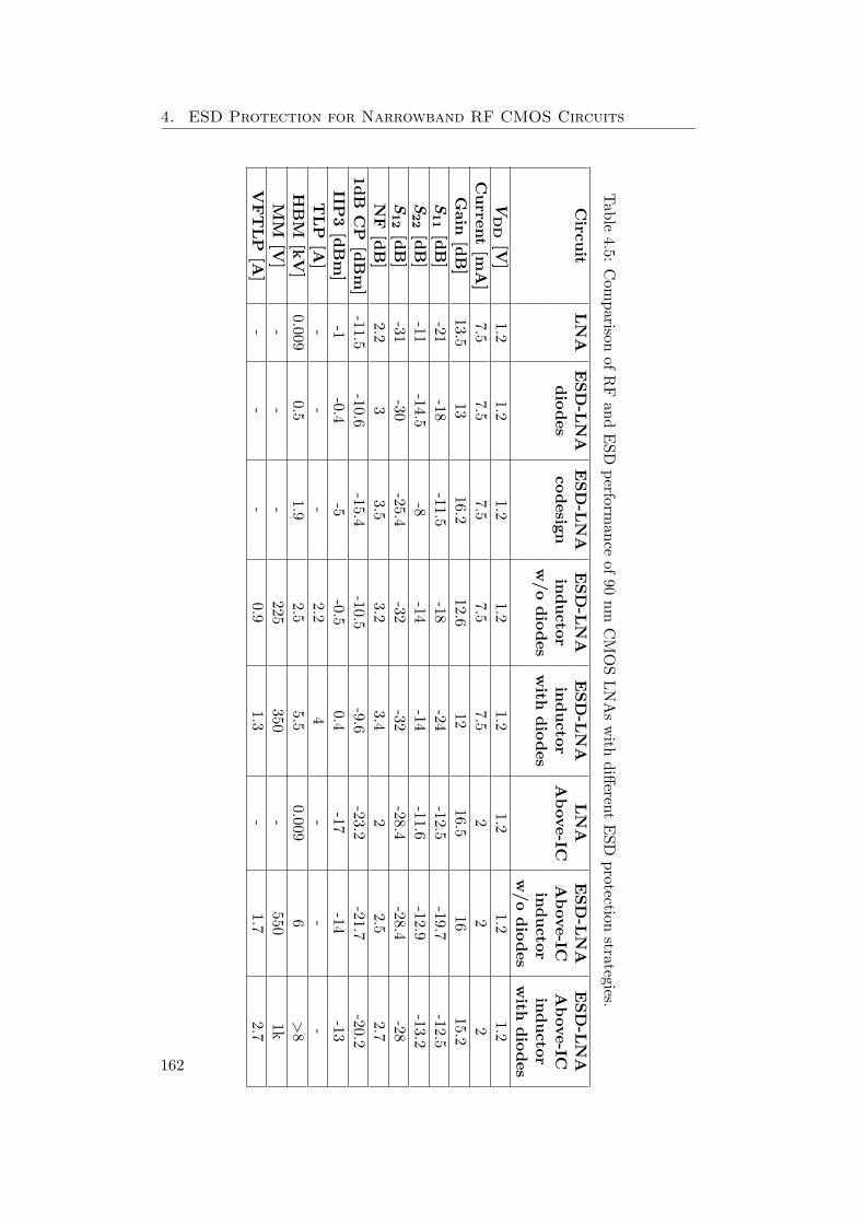
4. ESD Protection for Narrowband RF CMOS Circuits
Table
4.5:C
omparison
ofR
Fand
ESD
performance
of90
nmC
MO
SLN
As
with
differentE
SDprotection
strategies.
Circu
itLN
AESD
-LN
AESD
-LN
AESD
-LN
AESD
-LN
ALN
AESD
-LN
AESD
-LN
Adio
des
codesign
inductor
inductor
Above-IC
Above-IC
Above-IC
w/o
dio
des
with
dio
des
inductor
inductor
w/o
dio
des
with
dio
des
VD
D[V
]1.2
1.21.2
1.21.2
1.21.2
1.2C
urren
t[m
A]
7.57.5
7.57.5
7.52
22
Gain
[dB
]13.5
1316.2
12.612
16.516
15.2S
11
[dB
]-21
-18-11.5
-18-24
-12.5-19.7
-12.5S
22
[dB
]-11
-14.5-8
-14-14
-11.6-12.9
-13.2S
12
[dB
]-31
-30-25.4
-32-32
-28.4-28.4
-28N
F[d
B]
2.23
3.53.2
3.42
2.52.7
1dB
CP
[dB
m]
-11.5-10.6
-15.4-10.5
-9.6-23.2
-21.7-20.2
IIP3
[dB
m]
-1-0.4
-5-0.5
0.4-17
-14-13
TLP
[A]
--
-2.2
4-
--
HB
M[k
V]
0.0090.5
1.92.5
5.50.009
6>
8M
M[V
]-
--
225350
-550
1kV
FT
LP
[A]
--
-0.9
1.3-
1.72.7
162
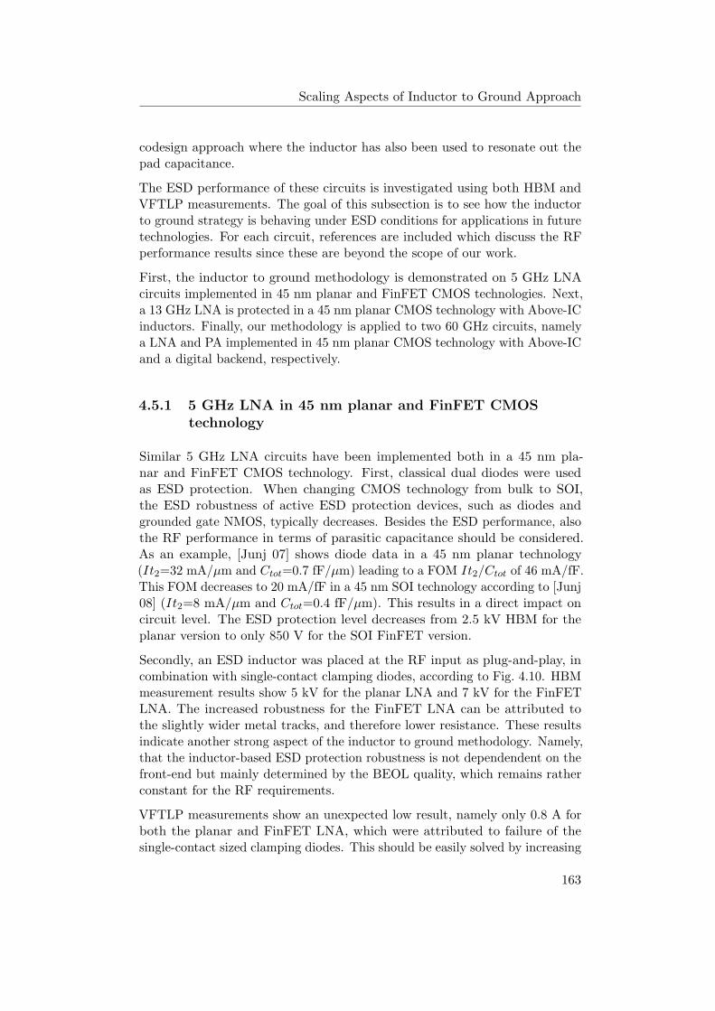
Scaling Aspects of Inductor to Ground Approach
codesign approach where the inductor has also been used to resonate out thepad capacitance.
The ESD performance of these circuits is investigated using both HBM andVFTLP measurements. The goal of this subsection is to see how the inductorto ground strategy is behaving under ESD conditions for applications in futuretechnologies. For each circuit, references are included which discuss the RFperformance results since these are beyond the scope of our work.
First, the inductor to ground methodology is demonstrated on 5 GHz LNAcircuits implemented in 45 nm planar and FinFET CMOS technologies. Next,a 13 GHz LNA is protected in a 45 nm planar CMOS technology with Above-ICinductors. Finally, our methodology is applied to two 60 GHz circuits, namelya LNA and PA implemented in 45 nm planar CMOS technology with Above-ICand a digital backend, respectively.
4.5.1 5 GHz LNA in 45 nm planar and FinFET CMOStechnology
Similar 5 GHz LNA circuits have been implemented both in a 45 nm pla-nar and FinFET CMOS technology. First, classical dual diodes were usedas ESD protection. When changing CMOS technology from bulk to SOI,the ESD robustness of active ESD protection devices, such as diodes andgrounded gate NMOS, typically decreases. Besides the ESD performance, alsothe RF performance in terms of parasitic capacitance should be considered.As an example, [Junj 07] shows diode data in a 45 nm planar technology(It2=32 mA/µm and Ctot=0.7 fF/µm) leading to a FOM It2/Ctot of 46 mA/fF.This FOM decreases to 20 mA/fF in a 45 nm SOI technology according to [Junj08] (It2=8 mA/µm and Ctot=0.4 fF/µm). This results in a direct impact oncircuit level. The ESD protection level decreases from 2.5 kV HBM for theplanar version to only 850 V for the SOI FinFET version.
Secondly, an ESD inductor was placed at the RF input as plug-and-play, incombination with single-contact clamping diodes, according to Fig. 4.10. HBMmeasurement results show 5 kV for the planar LNA and 7 kV for the FinFETLNA. The increased robustness for the FinFET LNA can be attributed tothe slightly wider metal tracks, and therefore lower resistance. These resultsindicate another strong aspect of the inductor to ground methodology. Namely,that the inductor-based ESD protection robustness is not dependendent on thefront-end but mainly determined by the BEOL quality, which remains ratherconstant for the RF requirements.
VFTLP measurements show an unexpected low result, namely only 0.8 A forboth the planar and FinFET LNA, which were attributed to failure of thesingle-contact sized clamping diodes. This should be easily solved by increasing
163
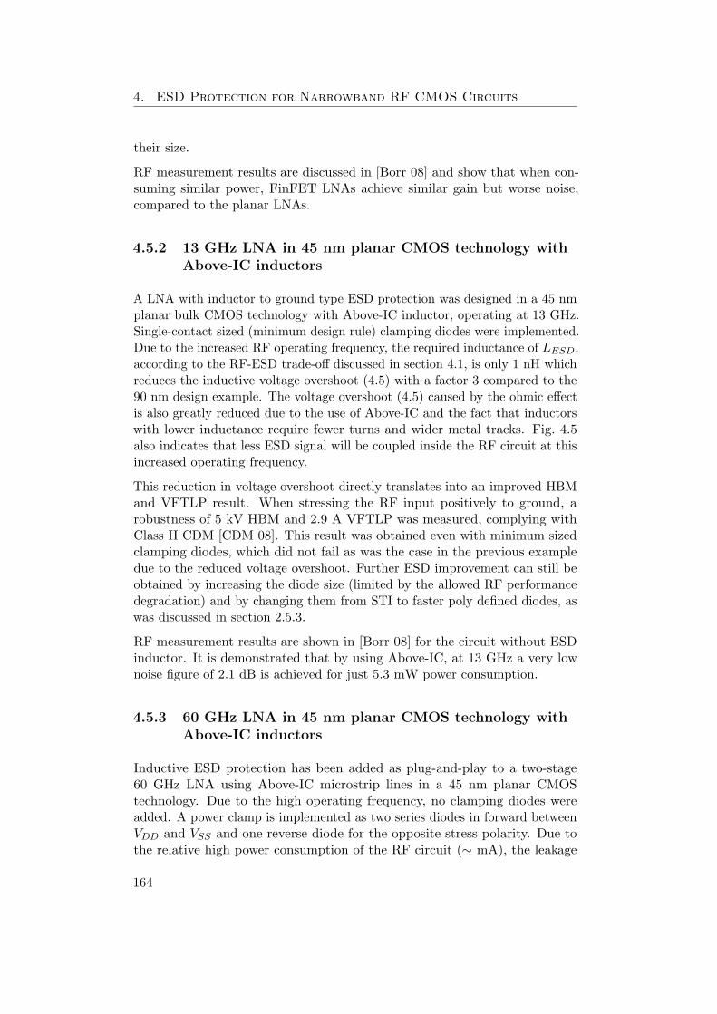
4. ESD Protection for Narrowband RF CMOS Circuits
their size.
RF measurement results are discussed in [Borr 08] and show that when con-suming similar power, FinFET LNAs achieve similar gain but worse noise,compared to the planar LNAs.
4.5.2 13 GHz LNA in 45 nm planar CMOS technology withAbove-IC inductors
A LNA with inductor to ground type ESD protection was designed in a 45 nmplanar bulk CMOS technology with Above-IC inductor, operating at 13 GHz.Single-contact sized (minimum design rule) clamping diodes were implemented.Due to the increased RF operating frequency, the required inductance of LESD,according to the RF-ESD trade-off discussed in section 4.1, is only 1 nH whichreduces the inductive voltage overshoot (4.5) with a factor 3 compared to the90 nm design example. The voltage overshoot (4.5) caused by the ohmic effectis also greatly reduced due to the use of Above-IC and the fact that inductorswith lower inductance require fewer turns and wider metal tracks. Fig. 4.5also indicates that less ESD signal will be coupled inside the RF circuit at thisincreased operating frequency.
This reduction in voltage overshoot directly translates into an improved HBMand VFTLP result. When stressing the RF input positively to ground, arobustness of 5 kV HBM and 2.9 A VFTLP was measured, complying withClass II CDM [CDM 08]. This result was obtained even with minimum sizedclamping diodes, which did not fail as was the case in the previous exampledue to the reduced voltage overshoot. Further ESD improvement can still beobtained by increasing the diode size (limited by the allowed RF performancedegradation) and by changing them from STI to faster poly defined diodes, aswas discussed in section 2.5.3.
RF measurement results are shown in [Borr 08] for the circuit without ESDinductor. It is demonstrated that by using Above-IC, at 13 GHz a very lownoise figure of 2.1 dB is achieved for just 5.3 mW power consumption.
4.5.3 60 GHz LNA in 45 nm planar CMOS technology withAbove-IC inductors
Inductive ESD protection has been added as plug-and-play to a two-stage60 GHz LNA using Above-IC microstrip lines in a 45 nm planar CMOStechnology. Due to the high operating frequency, no clamping diodes wereadded. A power clamp is implemented as two series diodes in forward betweenVDD and VSS and one reverse diode for the opposite stress polarity. Due tothe relative high power consumption of the RF circuit (∼ mA), the leakage
164
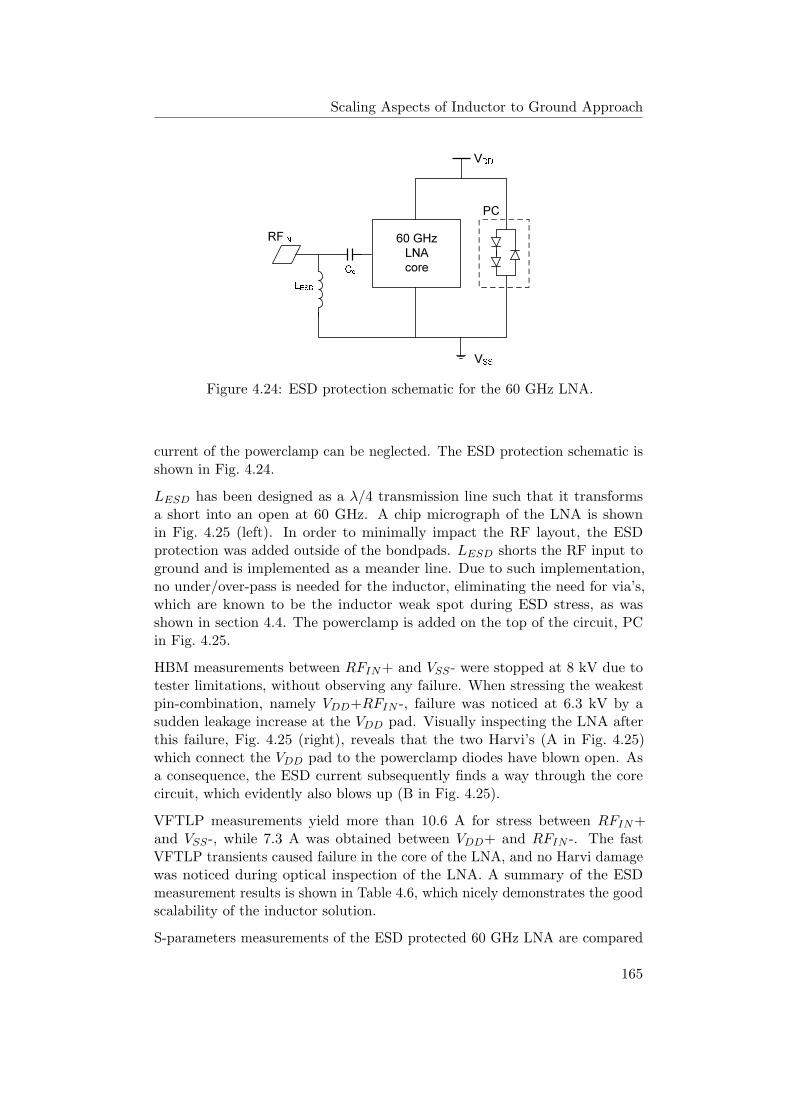
Scaling Aspects of Inductor to Ground Approach
CcVDD
RFIN LESD 60 GHzLNAcore
PC
VSSFigure 4.24: ESD protection schematic for the 60 GHz LNA.
current of the powerclamp can be neglected. The ESD protection schematic isshown in Fig. 4.24.
LESD has been designed as a λ/4 transmission line such that it transformsa short into an open at 60 GHz. A chip micrograph of the LNA is shownin Fig. 4.25 (left). In order to minimally impact the RF layout, the ESDprotection was added outside of the bondpads. LESD shorts the RF input toground and is implemented as a meander line. Due to such implementation,no under/over-pass is needed for the inductor, eliminating the need for via’s,which are known to be the inductor weak spot during ESD stress, as wasshown in section 4.4. The powerclamp is added on the top of the circuit, PCin Fig. 4.25.
HBM measurements between RFIN+ and VSS- were stopped at 8 kV due totester limitations, without observing any failure. When stressing the weakestpin-combination, namely VDD+RFIN -, failure was noticed at 6.3 kV by asudden leakage increase at the VDD pad. Visually inspecting the LNA afterthis failure, Fig. 4.25 (right), reveals that the two Harvi’s (A in Fig. 4.25)which connect the VDD pad to the powerclamp diodes have blown open. Asa consequence, the ESD current subsequently finds a way through the corecircuit, which evidently also blows up (B in Fig. 4.25).
VFTLP measurements yield more than 10.6 A for stress between RFIN+and VSS-, while 7.3 A was obtained between VDD+ and RFIN -. The fastVFTLP transients caused failure in the core of the LNA, and no Harvi damagewas noticed during optical inspection of the LNA. A summary of the ESDmeasurement results is shown in Table 4.6, which nicely demonstrates the goodscalability of the inductor solution.
S-parameters measurements of the ESD protected 60 GHz LNA are compared
165
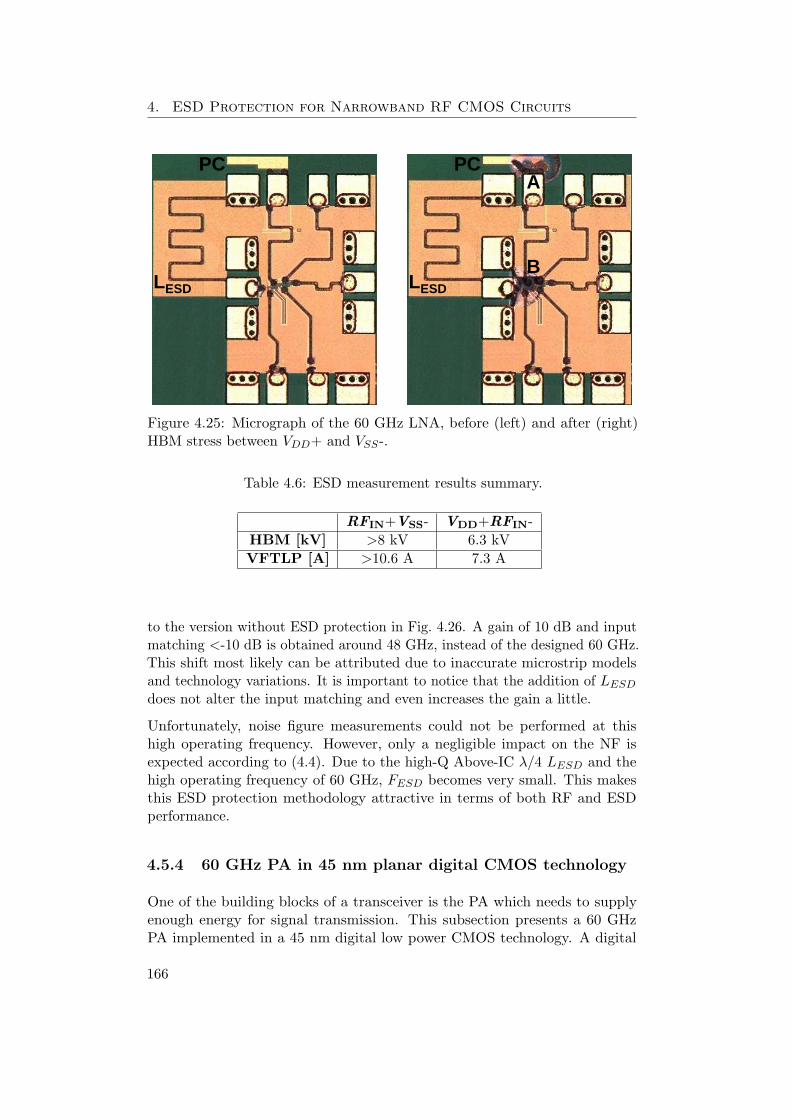
4. ESD Protection for Narrowband RF CMOS Circuits
LESD
PCA
BLESD
PC
Figure 4.25: Micrograph of the 60 GHz LNA, before (left) and after (right)HBM stress between VDD+ and VSS-.
Table 4.6: ESD measurement results summary.
RFIN+VSS- VDD+RFIN-HBM [kV] >8 kV 6.3 kVVFTLP [A] >10.6 A 7.3 A
to the version without ESD protection in Fig. 4.26. A gain of 10 dB and inputmatching <-10 dB is obtained around 48 GHz, instead of the designed 60 GHz.This shift most likely can be attributed due to inaccurate microstrip modelsand technology variations. It is important to notice that the addition of LESD
does not alter the input matching and even increases the gain a little.
Unfortunately, noise figure measurements could not be performed at thishigh operating frequency. However, only a negligible impact on the NF isexpected according to (4.4). Due to the high-Q Above-IC λ/4 LESD and thehigh operating frequency of 60 GHz, FESD becomes very small. This makesthis ESD protection methodology attractive in terms of both RF and ESDperformance.
4.5.4 60 GHz PA in 45 nm planar digital CMOS technology
One of the building blocks of a transceiver is the PA which needs to supplyenough energy for signal transmission. This subsection presents a 60 GHzPA implemented in a 45 nm digital low power CMOS technology. A digital
166
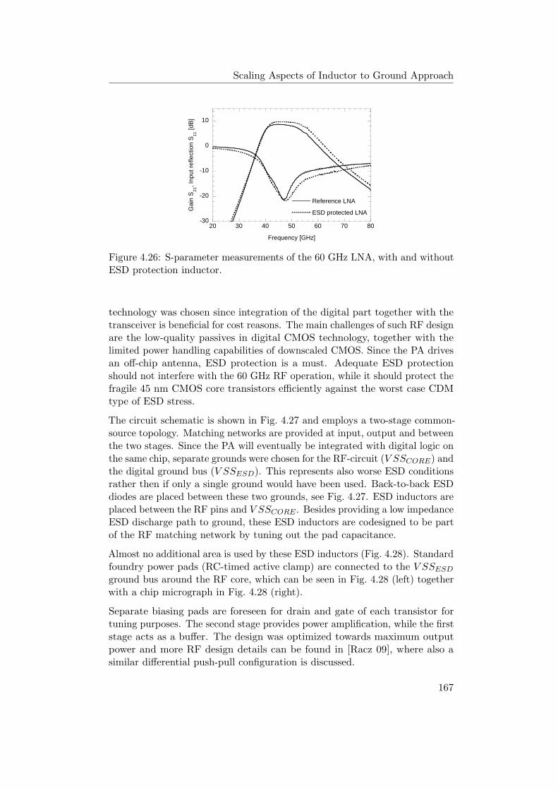
Scaling Aspects of Inductor to Ground Approach
-30
-20
-10
0
10
20 30 40 50 60 70 80
Reference LNA
ESD protected LNAGai
n S
21, I
nput
ref
lect
ion
S11
[dB
]
Frequency [GHz]
Figure 4.26: S-parameter measurements of the 60 GHz LNA, with and withoutESD protection inductor.
technology was chosen since integration of the digital part together with thetransceiver is beneficial for cost reasons. The main challenges of such RF designare the low-quality passives in digital CMOS technology, together with thelimited power handling capabilities of downscaled CMOS. Since the PA drivesan off-chip antenna, ESD protection is a must. Adequate ESD protectionshould not interfere with the 60 GHz RF operation, while it should protect thefragile 45 nm CMOS core transistors efficiently against the worst case CDMtype of ESD stress.
The circuit schematic is shown in Fig. 4.27 and employs a two-stage common-source topology. Matching networks are provided at input, output and betweenthe two stages. Since the PA will eventually be integrated with digital logic onthe same chip, separate grounds were chosen for the RF-circuit (V SSCORE) andthe digital ground bus (V SSESD). This represents also worse ESD conditionsrather then if only a single ground would have been used. Back-to-back ESDdiodes are placed between these two grounds, see Fig. 4.27. ESD inductors areplaced between the RF pins and V SSCORE . Besides providing a low impedanceESD discharge path to ground, these ESD inductors are codesigned to be partof the RF matching network by tuning out the pad capacitance.
Almost no additional area is used by these ESD inductors (Fig. 4.28). Standardfoundry power pads (RC-timed active clamp) are connected to the V SSESD
ground bus around the RF core, which can be seen in Fig. 4.28 (left) togetherwith a chip micrograph in Fig. 4.28 (right).
Separate biasing pads are foreseen for drain and gate of each transistor fortuning purposes. The second stage provides power amplification, while the firststage acts as a buffer. The design was optimized towards maximum outputpower and more RF design details can be found in [Racz 09], where also asimilar differential push-pull configuration is discussed.
167
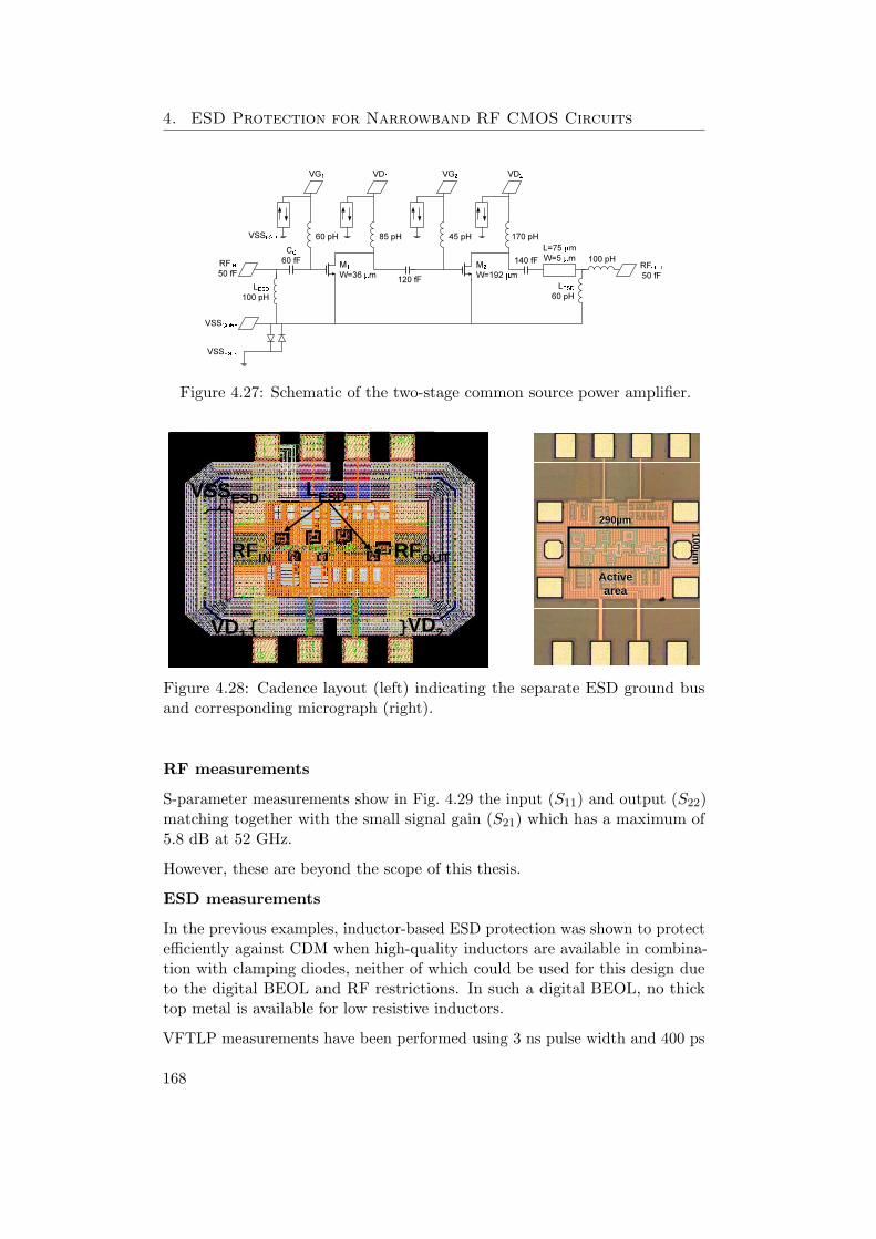
4. ESD Protection for Narrowband RF CMOS Circuits
M1W=36 m
RFIN50 fF
VSSCORECC
60 fF
LESD100 pH
VG1
VSSESD
60 pH
VD185 pH
120 fF
VG245 pH
VD2170 pH
M2W=192 m
140 fFL=75 mW=5 m
LESD60 pH
100 pH RFOUT50 fF
VSSESD
Figure 4.27: Schematic of the two-stage common source power amplifier.
VSSESD
RFINRFIN RFOUT
VD1 VD2
LESD
290µm
Activearea
100µm
Figure 4.28: Cadence layout (left) indicating the separate ESD ground busand corresponding micrograph (right).
RF measurements
S-parameter measurements show in Fig. 4.29 the input (S11) and output (S22)matching together with the small signal gain (S21) which has a maximum of5.8 dB at 52 GHz.
However, these are beyond the scope of this thesis.
ESD measurements
In the previous examples, inductor-based ESD protection was shown to protectefficiently against CDM when high-quality inductors are available in combina-tion with clamping diodes, neither of which could be used for this design dueto the digital BEOL and RF restrictions. In such a digital BEOL, no thicktop metal is available for low resistive inductors.
VFTLP measurements have been performed using 3 ns pulse width and 400 ps
168
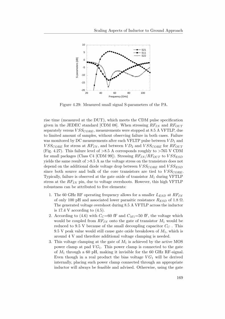
Scaling Aspects of Inductor to Ground Approach
-20
-15
-10
-5
0
5
10
20 40 60 80 100
S21S11S22
S-p
aram
eter
s [d
B]
Frequency [GHz]
Figure 4.29: Measured small signal S-parameters of the PA.
rise time (measured at the DUT), which meets the CDM pulse specificationgiven in the JEDEC standard [CDM 08]. When stressing RFIN and RFOUT
separately versus V SSCORE , measurements were stopped at 8.5 A VFTLP, dueto limited amount of samples, without observing failure in both cases. Failurewas monitored by DC measurements after each VFLTP pulse between V D1 andV SSCORE for stress at RFIN , and between V D2 and V SSCORE for RFOUT
(Fig. 4.27). This failure level of >8.5 A corresponds roughly to >765 V CDMfor small packages (Class C4 [CDM 99]). Stressing RFIN/RFOUT to V SSESD
yields the same result of >8.5 A as the voltage stress on the transistors does notdepend on the additional diode voltage drop between V SSCORE and V SSESD
since both source and bulk of the core transistors are tied to V SSCORE .Typically, failure is observed at the gate oxide of transistor M1 during VFTLPstress at the RFIN pin, due to voltage overshoots. However, this high VFTLProbustness can be attributed to five elements:
1. The 60 GHz RF operating frequency allows for a smaller LESD at RFIN
of only 100 pH and associated lower parasitic resistance RESD of 1.8 Ω.The generated voltage overshoot during 8.5 A VFTLP across the inductoris 17.4 V according to (4.5).
2. According to (4.6) with CC=60 fF and CM1=50 fF, the voltage whichwould be coupled from RFIN onto the gate of transistor M1 would bereduced to 9.5 V because of the small decoupling capacitor CC . This9.5 V peak value would still cause gate oxide breakdown of M1, which isaround 4 V and therefore additional voltage clamping is needed.
3. This voltage clamping at the gate of M1 is achieved by the active MOSpower clamp at pad V G1. This power clamp is connected to the gateof M1 through a 60 pH, making it invisible for the 60 GHz RF-signal.Even though in a real product the bias voltage V G1 will be derivedinternally, placing such power clamp connected through an appropriateinductor will always be feasible and advised. Otherwise, using the gate
169
4. ESD Protection for Narrowband RF CMOS Circuits
oxide failure voltage of 4 V for M1, a failure current of only 3.5 A canbe estimated according to (4.5) and (4.6), compared to >8.5 A withadditional inductor and power clamp. Note that this additional powerclamp has the same voltage clamping function as the clamping diodesshown in Fig. 4.10.
4. In case of RFOUT , the drain-junction of M2 has to be protected insteadof its gate, increasing the allowed voltage overshoots.
5. Metal-Oxide-Metal (MOM) capacitors were used instead of Metal-Insulator-Metal (MIM) capacitors because MIMs were not available in the digitalBEOL. Such MOM-type of capacitor is more robust than MIM due tothe thicker Inter-Metal Dielectric (IMD) layer compared to the MIMinsulator layer.
Since the inductor-to-ground methodology always requires a serial input ca-pacitance (CC), its impact on the performance of RFCMOS ICs should behighlighted. Ideally, the decoupling capacitor CC should be as large as possibleto remain invisible for the RF signal. However, the bigger the capacitanceis, the lower is its resonance frequency, puting a maximum boundary at thecapacitance value. Since the resonance frequency of the 60 fF capacitance issomewhat >100 GHz, it can be used for 60 GHz operation. However, it isrequired to take this capacitance into account during the design of the inputmatching network. The ESD inductor adds another degree of freedom whichcan be used to tune out the remaining capacitances, including the bondpadcapacitance, resulting in a very good input matching as seen in Fig. 4.29.
Since the voltage overshoot is not an issue, additional HBM measurementswere performed to apply ESD stress with more severe power content. For thesame pin combination as VFTLP, circuit failure is due to the ESD inductorsboth for RFIN and RFOUT . They fail during HBM to an open due to meltingof the tracks at 5.3 kV, see Fig. 4.30. Subsequently the MOM capacitor fails.
When stressing V D1 to V SSESD, >8.5 A VFTLP and 5 kV HBM is measured.However, when stressing to V SSCORE , only 4.4 A VFTLP is reached and 3 kVHBM. This indicates a parasitic current path through the core transistor M1
next to the intended ESD path through the power clamp. The gate of M1
is floating and gate coupling can induce MOS current. Eventually, bipolarcurrent will flow when breakdown of the drain-substrate junction is reached.In case of stress to V SSESD, the power clamp is competing with M1 in serieswith a diode. However, when stressing V D1 to V SSCORE , the diode switchessides and is now in the ESD current path and removed from the parasitic corepath. Therefore, more current will flow through M1, explaining the reducedrobustness for stress to V SSCORE .
When stressing V D1 versus RFIN , the ESD current has to travel first toV SSCORE via the power clamp and then through LESD to RFIN . Eventhough the drain to source voltage of the core transistor remains unaltered
170
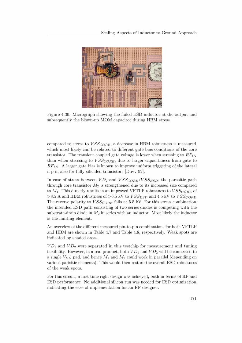
Scaling Aspects of Inductor to Ground Approach
Figure 4.30: Micrograph showing the failed ESD inductor at the output andsubsequently the blown-up MOM capacitor during HBM stress.
compared to stress to V SSCORE , a decrease in HBM robustness is measured,which most likely can be related to different gate bias conditions of the coretransistor. The transient coupled gate voltage is lower when stressing to RFIN
than when stressing to V SSCORE , due to larger capacitances from gate toRFIN . A larger gate bias is known to improve uniform triggering of the lateraln-p-n, also for fully silicided transistors [Duvv 92].
In case of stress between V D2 and V SSCORE/V SSESD, the parasitic paththrough core transistor M2 is strengthened due to its increased size comparedto M1. This directly results in an improved VFTLP robustness to V SSCORE of>8.5 A and HBM robustness of >6.5 kV to V SSESD and 4.5 kV to V SSCORE .The reverse polarity to V SSCORE fails at 5.5 kV. For this stress combination,the intended ESD path consisting of two series diodes is competing with thesubstrate-drain diode in M2 in series with an inductor. Most likely the inductoris the limiting element.
An overview of the different measured pin-to-pin combinations for both VFTLPand HBM are shown in Table 4.7 and Table 4.8, respectively. Weak spots areindicated by shaded areas.
V D1 and V D2 were separated in this testchip for measurement and tuningflexibility. However, in a real product, both V D1 and V D2 will be connected toa single VDD pad, and hence M1 and M2 could work in parallel (depending onvarious parisitic elements). This would then restore the overall ESD robustnessof the weak spots.
For this circuit, a first time right design was achieved, both in terms of RF andESD performance. No additional silicon run was needed for ESD optimization,indicating the ease of implementation for an RF designer.
171
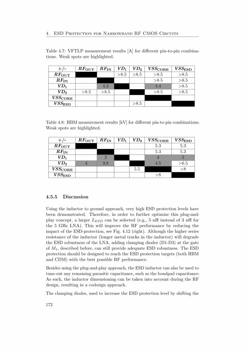
4. ESD Protection for Narrowband RF CMOS Circuits
Table 4.7: VFTLP measurement results [A] for different pin-to-pin combina-tions. Weak spots are highlighted.
+/- RFOUT RFIN VD1 VD2 VSSCORE VSSESD
RFOUT >8.5 >8.5 >8.5 >8.5RFIN >8.5 >8.5VD1 4.3 4.4 >8.5VD2 >8.5 >8.5 >8.5 >8.5
VSSCORE
VSSESD >8.5
Table 4.8: HBM measurement results [kV] for different pin-to-pin combinations.Weak spots are highlighted.
+/- RFOUT RFIN VD1 VD2 VSSCORE VSSESD
RFOUT 5.3 5.3RFIN 5.3 5.3VD1 2 3 5VD2 4 3.8 4.5 >6.5
VSSCORE 5.5 >8VSSESD >8
4.5.5 Discussion
Using the inductor to ground approach, very high ESD protection levels havebeen demonstrated. Therefore, in order to further optimize this plug-and-play concept, a larger LESD can be selected (e.g., 5 nH instead of 3 nH forthe 5 GHz LNA). This will improve the RF performance by reducing theimpact of the ESD-protection, see Fig. 4.12 (right). Although the higher seriesresistance of the inductor (longer metal tracks in the inductor) will degradethe ESD robustness of the LNA, adding clamping diodes (D1-D3) at the gateof M1, described before, can still provide adequate ESD robustness. The ESDprotection should be designed to reach the ESD protection targets (both HBMand CDM) with the best possible RF performance.
Besides using the plug-and-play approach, the ESD inductor can also be used totune-out any remaining parasitic capacitance, such as the bondpad capacitance.As such, the inductor dimensioning can be taken into account during the RFdesign, resulting in a codesign approach.
The clamping diodes, used to increase the ESD protection level by shifting the
172
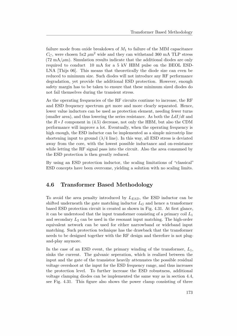
Transformer Based Methodology
failure mode from oxide breakdown of M1 to failure of the MIM capacitanceCC , were chosen 5x2 µm2 wide and they can withstand 360 mA TLP stress(72 mA/µm). Simulation results indicate that the additional diodes are onlyrequired to conduct 10 mA for a 5 kV HBM pulse on the BEOL ESD-LNA [Thijs 06]. This means that theoretically the diode size can even bereduced to minimum size. Such diodes will not introduce any RF performancedegradation, yet provide the additional ESD protection. However, enoughsafety margin has to be taken to ensure that these minimum sized diodes donot fail themselves during the transient stress.
As the operating frequencies of the RF circuits continue to increase, the RFand ESD frequency spectrum get more and more clearly separated. Hence,lower value inductors can be used as protection element, needing fewer turns(smaller area), and thus lowering the series resistance. As both the LdI/dt andthe R ∗ I component in (4.5) decrease, not only the HBM, but also the CDMperformance will improve a lot. Eventually, when the operating frequency ishigh enough, the ESD inductor can be implemented as a simple microstrip lineshortening input to ground (λ/4 line). In this way, all ESD stress is deviatedaway from the core, with the lowest possible inductance and on-resistancewhile letting the RF signal pass into the circuit. Also the area consumed bythe ESD protection is then greatly reduced.
By using an ESD protection inductor, the scaling limitations of “classical”ESD concepts have been overcome, yielding a solution with no scaling limits.
4.6 Transformer Based Methodology
To avoid the area penalty introduced by LESD, the ESD inductor can beshifted underneath the gate matching inductor LG and hence a transformerbased ESD protection circuit is created as shown in Fig. 4.31. At first glance,it can be understood that the input transformer consisting of a primary coil L1
and secondary L2 can be used in the resonant input matching. The high-orderequivalent network can be used for either narrowband or wideband inputmatching. Such protection technique has the drawback that the transformerneeds to be designed together with the RF design and therefore is not plug-and-play anymore.
In the case of an ESD event, the primary winding of the transformer, L1,sinks the current. The galvanic seperation, which is realized between theinput and the gate of the transistor heavily attenuates the possible residualvoltage overshoot at the input for the ESD frequency range, and thus increasesthe protection level. To further increase the ESD robustness, additionalvoltage clamping diodes can be implemented the same way as in section 4.4,see Fig. 4.31. This figure also shows the power clamp consisting of three
173
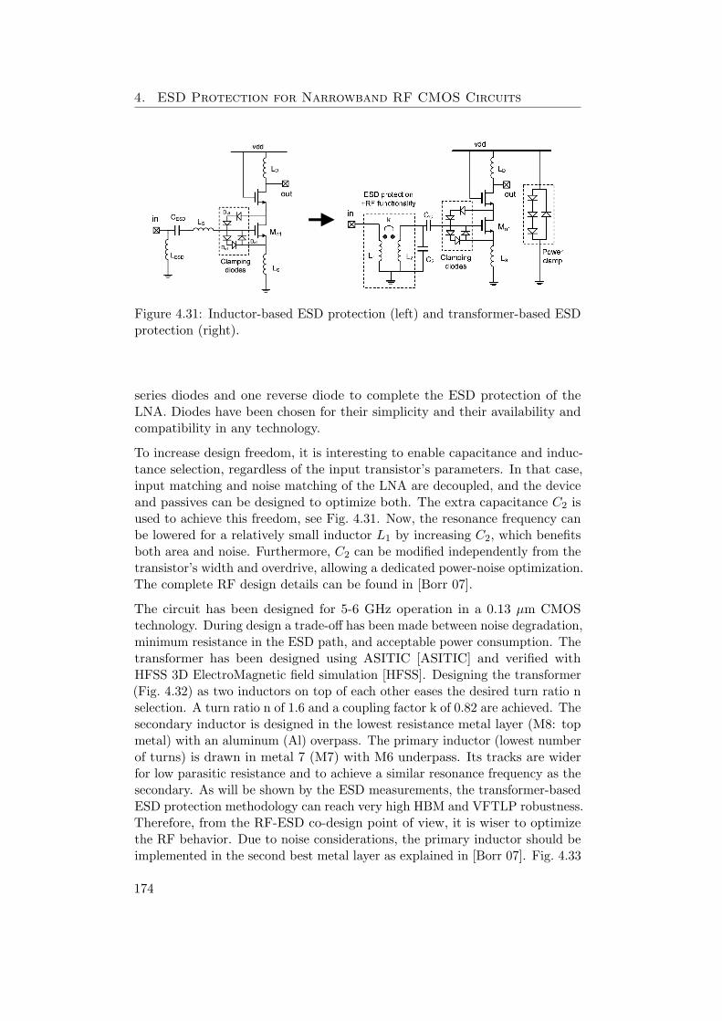
4. ESD Protection for Narrowband RF CMOS Circuits
Figure 4.31: Inductor-based ESD protection (left) and transformer-based ESDprotection (right).
series diodes and one reverse diode to complete the ESD protection of theLNA. Diodes have been chosen for their simplicity and their availability andcompatibility in any technology.
To increase design freedom, it is interesting to enable capacitance and induc-tance selection, regardless of the input transistor’s parameters. In that case,input matching and noise matching of the LNA are decoupled, and the deviceand passives can be designed to optimize both. The extra capacitance C2 isused to achieve this freedom, see Fig. 4.31. Now, the resonance frequency canbe lowered for a relatively small inductor L1 by increasing C2, which benefitsboth area and noise. Furthermore, C2 can be modified independently from thetransistor’s width and overdrive, allowing a dedicated power-noise optimization.The complete RF design details can be found in [Borr 07].
The circuit has been designed for 5-6 GHz operation in a 0.13 µm CMOStechnology. During design a trade-off has been made between noise degradation,minimum resistance in the ESD path, and acceptable power consumption. Thetransformer has been designed using ASITIC [ASITIC] and verified withHFSS 3D ElectroMagnetic field simulation [HFSS]. Designing the transformer(Fig. 4.32) as two inductors on top of each other eases the desired turn ratio nselection. A turn ratio n of 1.6 and a coupling factor k of 0.82 are achieved. Thesecondary inductor is designed in the lowest resistance metal layer (M8: topmetal) with an aluminum (Al) overpass. The primary inductor (lowest numberof turns) is drawn in metal 7 (M7) with M6 underpass. Its tracks are widerfor low parasitic resistance and to achieve a similar resonance frequency as thesecondary. As will be shown by the ESD measurements, the transformer-basedESD protection methodology can reach very high HBM and VFTLP robustness.Therefore, from the RF-ESD co-design point of view, it is wiser to optimizethe RF behavior. Due to noise considerations, the primary inductor should beimplemented in the second best metal layer as explained in [Borr 07]. Fig. 4.33
174
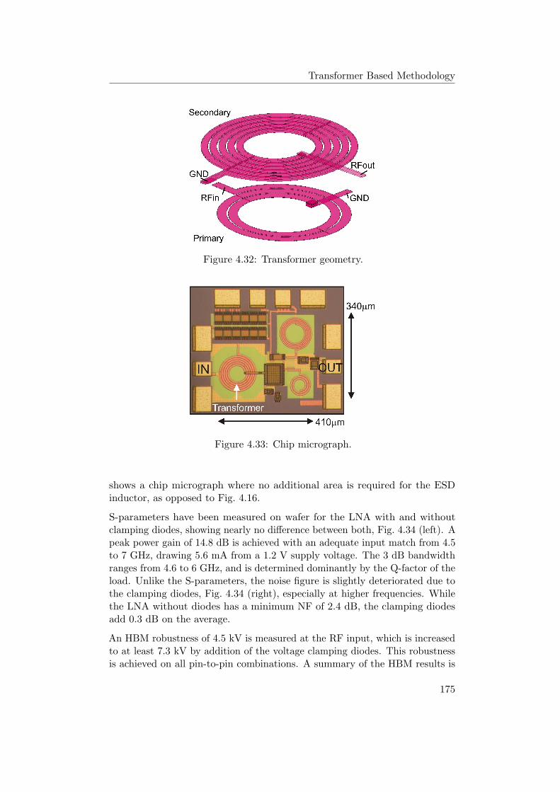
Transformer Based Methodology
Figure 4.32: Transformer geometry.
Figure 4.33: Chip micrograph.
shows a chip micrograph where no additional area is required for the ESDinductor, as opposed to Fig. 4.16.
S-parameters have been measured on wafer for the LNA with and withoutclamping diodes, showing nearly no difference between both, Fig. 4.34 (left). Apeak power gain of 14.8 dB is achieved with an adequate input match from 4.5to 7 GHz, drawing 5.6 mA from a 1.2 V supply voltage. The 3 dB bandwidthranges from 4.6 to 6 GHz, and is determined dominantly by the Q-factor of theload. Unlike the S-parameters, the noise figure is slightly deteriorated due tothe clamping diodes, Fig. 4.34 (right), especially at higher frequencies. Whilethe LNA without diodes has a minimum NF of 2.4 dB, the clamping diodesadd 0.3 dB on the average.
An HBM robustness of 4.5 kV is measured at the RF input, which is increasedto at least 7.3 kV by addition of the voltage clamping diodes. This robustnessis achieved on all pin-to-pin combinations. A summary of the HBM results is
175
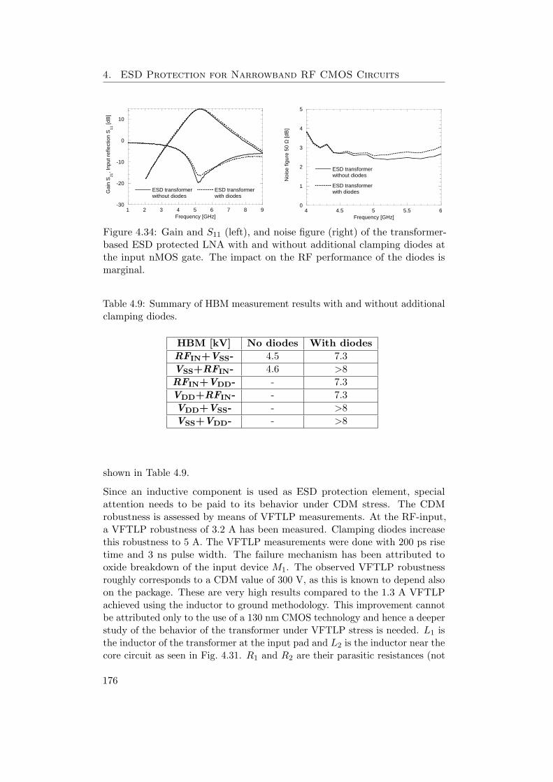
4. ESD Protection for Narrowband RF CMOS Circuits
1 2 3 4 5 6 7 8 9
ESD transformerwithout diodes
ESD transformerwith diodes
-30
-20
-10
0
10
Gai
n S
21, I
nput
ref
lect
ion
S11
[dB
]
Frequency [GHz]4 4.5 5 5.5 6
ESD transformerwithout diodes
ESD transformerwith diodes
0
1
2
3
4
5
Noi
se fi
gure
50
Ω [d
B]
Frequency [GHz]
Figure 4.34: Gain and S11 (left), and noise figure (right) of the transformer-based ESD protected LNA with and without additional clamping diodes atthe input nMOS gate. The impact on the RF performance of the diodes ismarginal.
Table 4.9: Summary of HBM measurement results with and without additionalclamping diodes.
HBM [kV] No diodes With diodesRFIN+VSS- 4.5 7.3VSS+RFIN- 4.6 >8RFIN+VDD- - 7.3VDD+RFIN- - 7.3VDD+VSS- - >8VSS+VDD- - >8
shown in Table 4.9.
Since an inductive component is used as ESD protection element, specialattention needs to be paid to its behavior under CDM stress. The CDMrobustness is assessed by means of VFTLP measurements. At the RF-input,a VFTLP robustness of 3.2 A has been measured. Clamping diodes increasethis robustness to 5 A. The VFTLP measurements were done with 200 ps risetime and 3 ns pulse width. The failure mechanism has been attributed tooxide breakdown of the input device M1. The observed VFTLP robustnessroughly corresponds to a CDM value of 300 V, as this is known to depend alsoon the package. These are very high results compared to the 1.3 A VFTLPachieved using the inductor to ground methodology. This improvement cannotbe attributed only to the use of a 130 nm CMOS technology and hence a deeperstudy of the behavior of the transformer under VFTLP stress is needed. L1 isthe inductor of the transformer at the input pad and L2 is the inductor near thecore circuit as seen in Fig. 4.31. R1 and R2 are their parasitic resistances (not
176
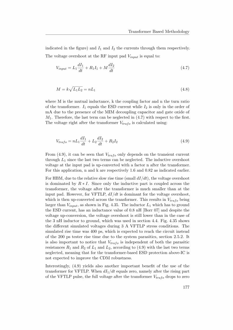
Transformer Based Methodology
indicated in the figure) and I1 and I2 the currents through them respectively.
The voltage overshoot at the RF input pad Vinput is equal to:
Vinput = L1dI1
dt+ R1I1 + M
dI2
dt(4.7)
M = k√
L1L2 = nL1 (4.8)
where M is the mutual inductance, k the coupling factor and n the turn ratioof the transformer. I1 equals the ESD current while I2 is only in the order ofmA due to the presence of the MIM decoupling capacitor and gate oxide ofM1. Therefore, the last term can be neglected in (4.7) with respect to the first.The voltage right after the transformer Vtrafo is calculated using:
Vtrafo = nL1dI1
dt+ L2
dI2
dt+ R2I2 (4.9)
From (4.9), it can be seen that Vtrafo only depends on the transient currentthrough L1 since the last two terms can be neglected. The inductive overshootvoltage at the input pad is up-converted with a factor n after the transformer.For this application, n and k are respectively 1.6 and 0.82 as indicated earlier.
For HBM, due to the relative slow rise time (small dI/dt), the voltage overshootis dominated by R ∗ I. Since only the inductive part is coupled across thetransformer, the voltage after the transformer is much smaller than at theinput pad. However, for VFTLP, dI/dt is dominant for the voltage overshoot,which is then up-converted across the transformer. This results in Vtrafo beinglarger than Vinput, as shown in Fig. 4.35. The inductor L1 which has to groundthe ESD current, has an inductance value of 0.8 nH [Borr 07] and despite thevoltage up-conversion, the voltage overshoot is still lower than in the case ofthe 3 nH inductor to ground, which was used in section 4.4. Fig. 4.35 showsthe different simulated voltages during 3 A VFTLP stress conditions. Thesimulated rise time was 400 ps, which is expected to reach the circuit insteadof the 200 ps tester rise time due to the system parasitics, section 2.5.2. Itis also important to notice that Vtrafo is independent of both the parasiticresistances R1 and R2 of L1 and L2, according to (4.9) with the last two termsneglected, meaning that for the transformer-based ESD protection above-IC isnot expected to improve the CDM robustness.
Interestingly, (4.9) yields also another important benefit of the use of thetransformer for VFTLP. When dI1/dt equals zero, namely after the rising partof the VFTLP pulse, the full voltage after the transformer Vtrafo drops to zero
177
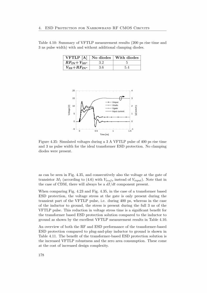
4. ESD Protection for Narrowband RF CMOS Circuits
Table 4.10: Summary of VFTLP measurement results (200 ps rise time and3 ns pulse width) with and without additional clamping diodes.
VFTLP [A] No diodes With diodesRFIN+VSS- 3.2 5VSS+RFIN- 3.6 5.4
-5
0
5
10
15
20
-1
0
1
2
3
4
0 0.5 1 1.5
VinputVtrafoVgateInput current
Vol
tage
[V] C
urrent [A]
Time [ns]
Figure 4.35: Simulated voltages during a 3 A VFTLP pulse of 400 ps rise timeand 3 ns pulse width for the ideal transformer ESD protection. No clampingdiodes were present.
as can be seen in Fig. 4.35, and consecutively also the voltage at the gate oftransistor M1 (according to (4.6) with Vtrafo instead of Vinput). Note that inthe case of CDM, there will always be a dI/dt component present.
When comparing Fig. 4.23 and Fig. 4.35, in the case of a transformer basedESD protection, the voltage stress at the gate is only present during thetransient part of the VFTLP pulse, i.e. during 400 ps, whereas in the caseof the inductor to ground, the stress is present during the full 3 ns of theVFTLP pulse. This reduction in voltage stress time is a significant benefit forthe transformer based ESD protection solution compared to the inductor toground as shown by the excellent VFTLP measurement results in Table 4.10.
An overview of both the RF and ESD performance of the transformer-basedESD protection compared to plug-and-play inductor to ground is shown inTable 4.11. The benefit of the transformer-based ESD protection solution isthe increased VFTLP robustness and the zero area consumption. These comeat the cost of increased design complexity.
178
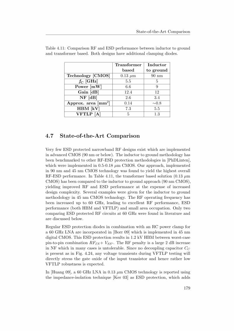
State-of-the-Art Comparison
Table 4.11: Comparison RF and ESD performance between inductor to groundand transformer based. Both designs have additional clamping diodes.
Transformer Inductorbased to ground
Technology [CMOS] 0.13 µm 90 nmfC [GHz] 5.5 5
Power [mW] 6.6 9Gain [dB] 12.4 12NF [dB] 2.6 3.4
Approx. area [mm2] 0.14 ∼0.8HBM [kV] 7.3 5.5VFTLP [A] 5 1.3
4.7 State-of-the-Art Comparison
Very few ESD protected narrowband RF designs exist which are implementedin advanced CMOS (90 nm or below). The inductor to ground methodology hasbeen benchmarked to other RF-ESD protection methodologies in [PhDLinten],which were implemented in 0.5-0.18 µm CMOS. Our approach, implementedin 90 nm and 45 nm CMOS technology was found to yield the highest overallRF-ESD performance. In Table 4.11, the transformer based solution (0.13 µmCMOS) has been compared to the inductor to ground approach (90 nm CMOS),yielding improved RF and ESD performance at the expense of increaseddesign complexity. Several examples were given for the inductor to groundmethodology in 45 nm CMOS technology. The RF operating frequency hasbeen increased up to 60 GHz, leading to excellent RF performance, ESDperformance (both HBM and VFTLP) and small area occupation. Only twocomparing ESD protected RF circuits at 60 GHz were found in literature andare discussed below.
Regular ESD protection diodes in combination with an RC power clamp fora 60 GHz LNA are incorporated in [Borr 09] which is implemented in 45 nmdigital CMOS. This ESD protection results in 1.2 kV HBM between worst-casepin-to-pin combination RFIN+ VSS-. The RF penalty is a large 2 dB increasein NF which in many cases is untolerable. Since no decoupling capacitor CC
is present as in Fig. 4.24, any voltage transients during VFTLP testing willdirectly stress the gate oxide of the input transistor and hence rather lowVFTLP robustness is expected.
In [Huang 09], a 60 GHz LNA in 0.13 µm CMOS technology is reported usingthe impedance-isolation technique [Ker 03] as ESD protection, which adds
179
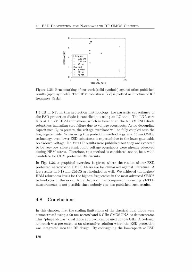
4. ESD Protection for Narrowband RF CMOS Circuits
0
2
4
6
8
1 10 100
0.18 um0.13 um45 nm
130 nm90 nm45 nm
HB
M le
vel [
kV]
Frequency [GHz]
Literature
Our work
Figure 4.36: Benchmarking of our work (solid symbols) against other publishedresults (open symbols). The HBM robustness [kV] is plotted as function of RFfrequency [GHz].
1.5 dB in NF. In this protection methodology, the parasitic capacitance ofthe ESD protection diode is cancelled out using an LC-tank. The LNA corefails at 1.5 kV HBM robustness, which is lower than the 6.5 kV ESD dioderobustness indicating core failure due to voltage overshoots. As no decouplingcapacitance CC is present, the voltage overshoot will be fully coupled onto thefragile gate oxide. When using this protection methodology in a 45 nm CMOStechnology, even lower ESD robustness is expected due to the lower gate oxidebreakdown voltage. No VFTLP results were published but they are expectedto be very low since catastrophic voltage overshoots were already observedduring HBM stress. Therefore, this method is considered not to be a validcandidate for CDM protected RF circuits.
In Fig. 4.36, a graphical overview is given, where the results of our ESDprotected narrowband CMOS LNAs are benchmarked against literature. Afew results in 0.18 µm CMOS are included as well. We achieved the highestHBM robustness levels for the highest frequencies in the most advanced CMOStechnologies in the world. Note that a similar comparison regarding VFTLPmeasurements is not possible since nobody else has published such results.
4.8 Conclusions
In this chapter, first the scaling limitations of the classical dual diode weredemonstrated using a 90 nm narrowband 5 GHz CMOS LNA as demonstrator.This “plug-and-play” dual diode approach can be used up to 5 GHz. A codesignapproach was presented as an alternative solution where the ESD protectionwas integrated into the RF design. By codesigning the low-capacitive ESD
180
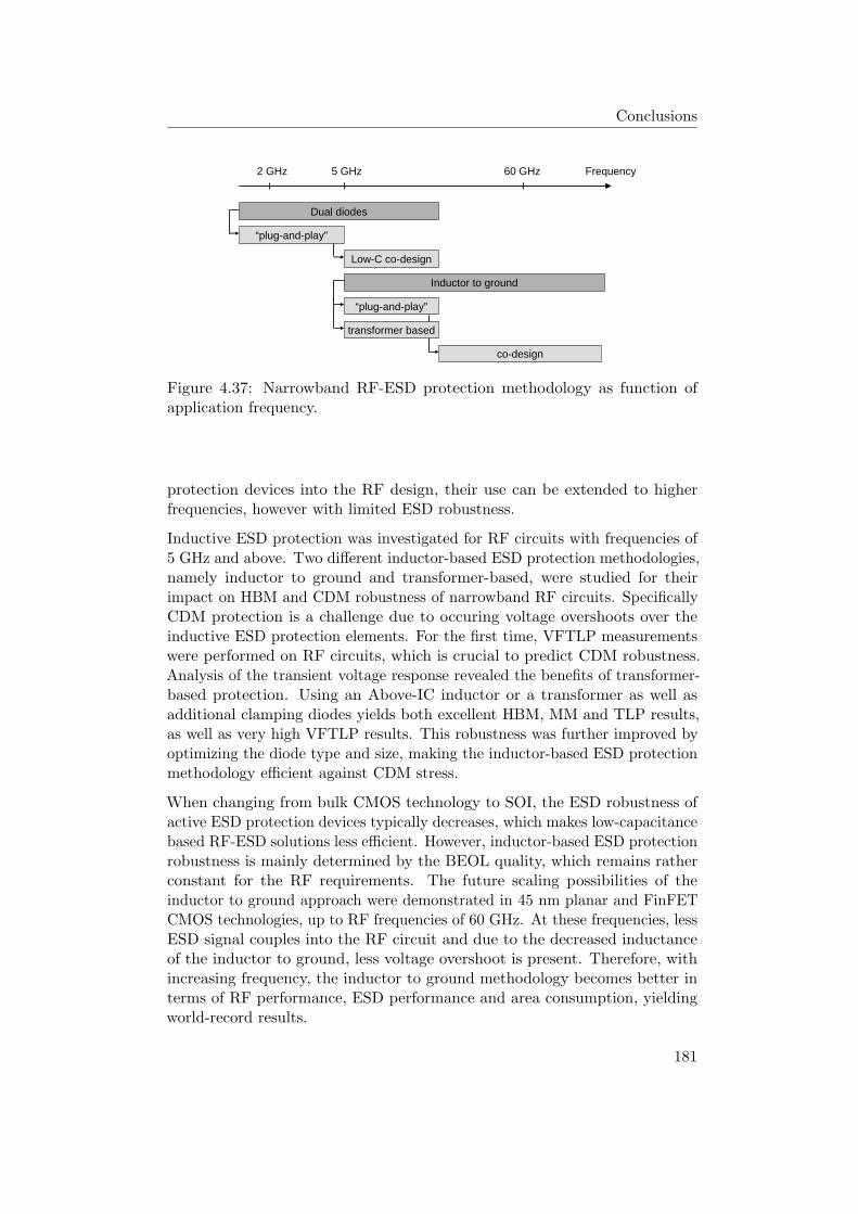
Conclusions
Frequency60 GHz5 GHz2 GHz
Dual diodes
“plug-and-play”
Low-C co-design
Inductor to ground
“plug-and-play”
transformer based
co-design
Figure 4.37: Narrowband RF-ESD protection methodology as function ofapplication frequency.
protection devices into the RF design, their use can be extended to higherfrequencies, however with limited ESD robustness.
Inductive ESD protection was investigated for RF circuits with frequencies of5 GHz and above. Two different inductor-based ESD protection methodologies,namely inductor to ground and transformer-based, were studied for theirimpact on HBM and CDM robustness of narrowband RF circuits. SpecificallyCDM protection is a challenge due to occuring voltage overshoots over theinductive ESD protection elements. For the first time, VFTLP measurementswere performed on RF circuits, which is crucial to predict CDM robustness.Analysis of the transient voltage response revealed the benefits of transformer-based protection. Using an Above-IC inductor or a transformer as well asadditional clamping diodes yields both excellent HBM, MM and TLP results,as well as very high VFTLP results. This robustness was further improved byoptimizing the diode type and size, making the inductor-based ESD protectionmethodology efficient against CDM stress.
When changing from bulk CMOS technology to SOI, the ESD robustness ofactive ESD protection devices typically decreases, which makes low-capacitancebased RF-ESD solutions less efficient. However, inductor-based ESD protectionrobustness is mainly determined by the BEOL quality, which remains ratherconstant for the RF requirements. The future scaling possibilities of theinductor to ground approach were demonstrated in 45 nm planar and FinFETCMOS technologies, up to RF frequencies of 60 GHz. At these frequencies, lessESD signal couples into the RF circuit and due to the decreased inductanceof the inductor to ground, less voltage overshoot is present. Therefore, withincreasing frequency, the inductor to ground methodology becomes better interms of RF performance, ESD performance and area consumption, yieldingworld-record results.
181
4. ESD Protection for Narrowband RF CMOS Circuits
By an increased design effort, the inductor to ground methodology can bechanged into a transformer based protection scheme with decreased area con-sumption and improved ESD robustness. However, given the excellent RF andESD performance of the “plug-and-play” inductor to ground for circuits withincreased operating frequency, the inductor to ground methodology is preferredover the transformer based solution because of the reduced design complexity.Integration of the inductor to ground methodology is straightforward for an RFdesigner since the impact on the RF performance can easily be simulated. TheESD inductor can even be used to tune out any remaining parasitic capacitancein a codesign approach. Therefore, using an inductor to ground is an excellentcandidate for ESD protection for narrowband mm-wave applications.
A graphical overview of the different narrowband RF-ESD protection strategiesis given in Fig. 4.37 as function of application frequency.
182
Chapter 5
ESD Protection forWideband RF CMOS Circuits
As wideband RF circuits are getting implemented in CMOS, there is a need foradequate ESD protection for these circuits. Current solutions are either limitedin terms of RF performance, power consumption, ESD performance and/orarea consumption. In this work we present a novel T-diode-based solutionas an excellent plug-and-play candidate yielding both excellent RF and ESDperformance using limited amount of area. For extreme wideband DistributedAmplifiers (DA), a Center Balanced Distributed ESD (CBDESD) protection isproposed without the need for redesign of each gain stage.
5.1 Introduction
Wireless communications are expanding with increasing number of applicationstandards such as Wireless Local Access Network (WLAN), Ultra WideBand(UWB), Wideband Code Division Multiple Access (WCDMA), etc., all opera-ting at different carrier frequencies. This results in an increasing interest in therealization of multi-standard transceivers in mainstream CMOS technologies.One possible realization is a Software-Defined Wireless Receiver [Bagh 06],where the entire available signal band is received at the input of one widebandRF LNA.
Such a wideband RF LNA needs ESD protection at its RF input pin, whilemaintaining adequate input matching over the entire operating frequency band.Narrowband cancellation techniques as discussed in the previous chapter,cannot be used as they only provide input matching around a certain frequencyand not over a wide band.
5. ESD Protection for Wideband RF CMOS Circuits
In this chapter, we propose two ESD solutions for wideband RF applications.First, in section 5.2, the concept “T-diode” is introduced as a candidate forplug-and-play ESD protection for wideband circuits. In addition, a genericmethodology is demonstrated on the T-diode to prevent circuit failure due toparasitic current paths inside the core circuit. This methodology is also widelyapplicable for narrowband RF circuits, and even for any other type of circuit.Secondly, a distributed ESD concept called Center Balanced Distributed ESDprotection (CB-DESD) is implemented for a DA in section 5.3. Finally insection 5.4 a comparison is made with the state-of-the-art publications on ESDprotected wideband RF circuits.
5.2 T-diodes
This section introduces a novel “plug-and-play” “T-diode” ESD protectionmethodology for wideband RF circuits, consisting of an integrated transformerand ESD diodes. The technique requires no additional power consumption,and maintains the full RF bandwidth.
First, the T-diode design methodology is discussed in section 5.2.1. Section 5.2.2and section 5.2.3 present two design examples implemented in a 0.18 µm anda 90 nm CMOS technology respectively. RF and ESD results are discussed indetail. Finally, a general method to avoid triggering of parasitic current pathsin the functional core circuit during ESD stress is described in section 5.2.4.
5.2.1 T-diode design methodology
An ESD protection circuit for a wideband RF amplifier needs to maintain agood input matching of the amplifier over its entire bandwidth.
The classical dual-diode ESD protection, as shown in Fig. 5.1 (left), is ratherunsuitable for protecting the input of a wideband RF amplifier, as the totalcapacitive load added by the diodes D1 and D2 (CD) deteriorates the inputimpedance reducing the overall bandwidth of the amplifier [Sold 05]. Forexample a 2x230 fF capacitive ESD load has an impedance of 346 Ω at 1 GHz,69 Ω at 5 GHz, and 45 Ω at 10 GHz. When placed in parallel with the 50 Ωinput impedance of the amplifier, the overall input matching is considerablylowered, and hence degraded.
A method to overcome this bandwidth limiting problem is proposed, referred toas T-diodes (transformer plus diodes), which use two coupled inductors L1, L2,and a capacitor Cc in Fig. 5.1 (right). Together with the capacitances of diodeD1 and D2 (CD) at the specific LNA bias voltage used, the structure closelyapproximates a lossless transmission line [Horng 03] as shown in Fig. 5.2.
184
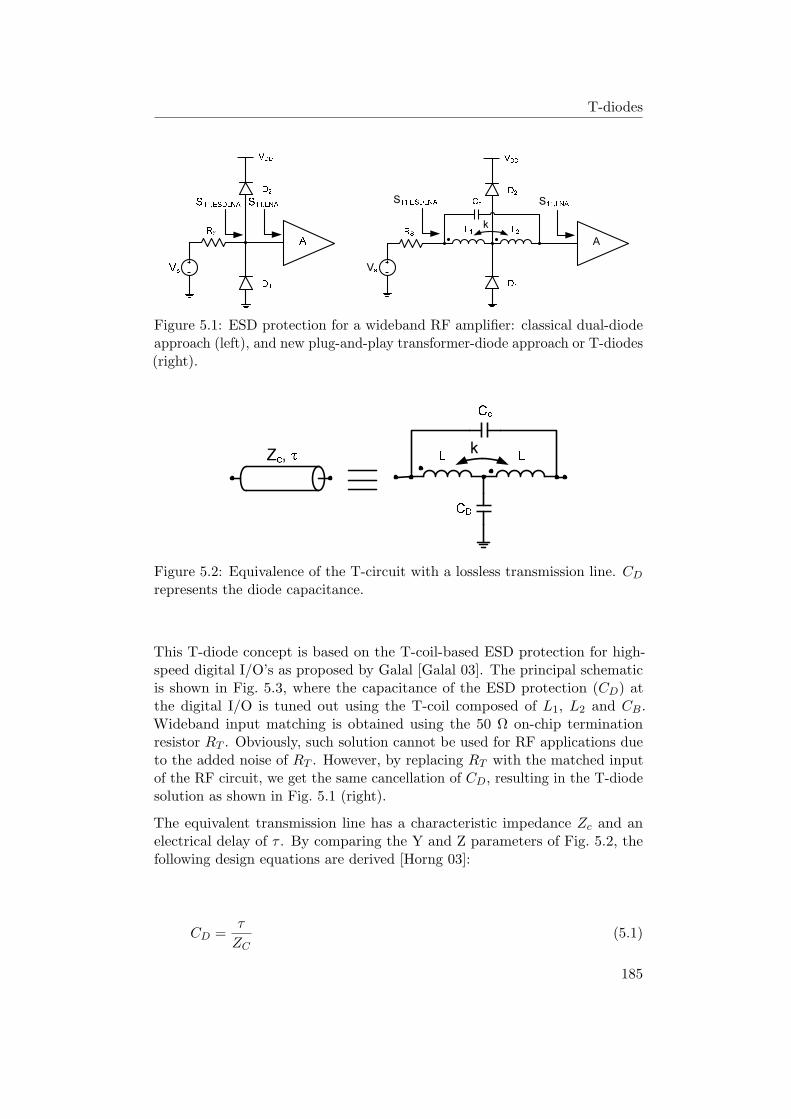
T-diodes
AD2D1VDD
Vs RSS11,ESDLNA S11,LNAA
L1 L2D2D1VDD
k
CcVs RSS11,ESDLNA S11,LNA
Figure 5.1: ESD protection for a wideband RF amplifier: classical dual-diodeapproach (left), and new plug-and-play transformer-diode approach or T-diodes(right).
L Lk
CcCDZc,
Figure 5.2: Equivalence of the T-circuit with a lossless transmission line. CD
represents the diode capacitance.
This T-diode concept is based on the T-coil-based ESD protection for high-speed digital I/O’s as proposed by Galal [Galal 03]. The principal schematicis shown in Fig. 5.3, where the capacitance of the ESD protection (CD) atthe digital I/O is tuned out using the T-coil composed of L1, L2 and CB.Wideband input matching is obtained using the 50 Ω on-chip terminationresistor RT . Obviously, such solution cannot be used for RF applications dueto the added noise of RT . However, by replacing RT with the matched inputof the RF circuit, we get the same cancellation of CD, resulting in the T-diodesolution as shown in Fig. 5.1 (right).
The equivalent transmission line has a characteristic impedance Zc and anelectrical delay of τ . By comparing the Y and Z parameters of Fig. 5.2, thefollowing design equations are derived [Horng 03]:
CD =τ
ZC(5.1)
185
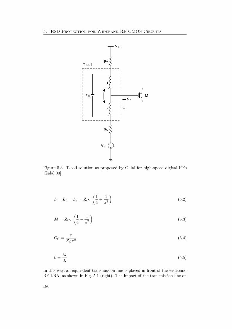
5. ESD Protection for Wideband RF CMOS Circuits
L1L2CC CDRS
RT VDD
Vs
T-coil
M
Figure 5.3: T-coil solution as proposed by Galal for high-speed digital IO’s[Galal 03].
L = L1 = L2 = ZCτ
(14
+1π2
)(5.2)
M = ZCτ
(14− 1
π2
)(5.3)
CC =τ
ZCπ2(5.4)
k =M
L(5.5)
In this way, an equivalent transmission line is placed in front of the widebandRF LNA, as shown in Fig. 5.1 (right). The impact of the transmission line on
186
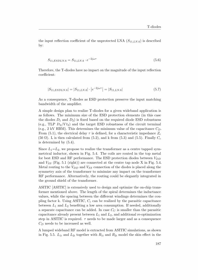
T-diodes
the input reflection coefficient of the unprotected LNA (S11,LNA) is describedby:
S11,ESDLNA = S11,LNA · e−2jωτ (5.6)
Therefore, the T-diodes have no impact on the magnitude of the input reflectioncoefficient:
|S11,ESDLNA| = |S11,LNA| ·∣∣e−2jωτ
∣∣ = |S11,LNA| (5.7)
As a consequence, T-diodes as ESD protection preserve the input matchingbandwidth of the amplifier.
A simple design plan to realize T-diodes for a given wideband application isas follows. The minimum size of the ESD protection elements (in this casethe diodes D1 and D2) is fixed based on the required diode ESD robustness(e.g., TLP It2/V t2) and the target ESD robustness of the circuit terminal(e.g., 2 kV HBM). This determines the minimum value of the capacitance CD.From (5.1), the electrical delay τ is defined, for a characteristic impedance Zc
(50 Ω). L is then calculated from (5.2), and k from (5.3) and (5.5). Finally Cc
is determined by (5.4).
Since L1=L2, we propose to realize the transformer as a centre tapped sym-metrical inductor, shown in Fig. 5.4. The coils are routed in the top metalfor best ESD and RF performance. The ESD protection diodes between VDD
and VSS (Fig. 5.1 (right)) are connected at the centre tap node X in Fig. 5.4.Metal routing to the VDD and VSS connection of the diodes is placed along thesymmetry axis of the transformer to minimize any impact on the transformerRF performance. Alternatively, the routing could be elegantly integrated inthe ground shield of the transformer.
ASITIC [ASITIC] is extensively used to design and optimize the on-chip trans-former mentioned above. The length of the spiral determines the inductancevalues, while the spacing between the different windings determines the cou-pling factor k. Using ASITIC, Cc can be realized by the parasitic capacitancebetween L1 and L2 benefiting a low area consumption. If needed, additionallya separate capacitance can be added. In case CC is smaller than the parasiticcapacitance already present between L1 and L2, and additional re-optimizationstep in ASITIC is required. τ needs to be made larger and as a consequenceCD needs to be increased as well.
A lumped wideband RF model is extracted from ASITIC simulations, as shownin Fig. 5.5. L1i and L2i together with R1i and R2i model the skin effect in the
187
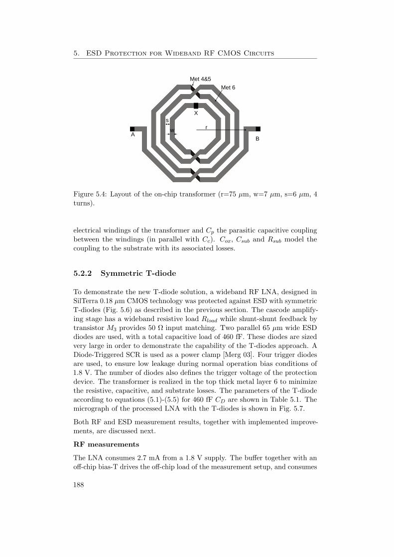
5. ESD Protection for Wideband RF CMOS Circuits
wA
B
Xs
Met 6
Met 4&5
r
Figure 5.4: Layout of the on-chip transformer (r=75 µm, w=7 µm, s=6 µm, 4turns).
electrical windings of the transformer and Cp the parasitic capacitive couplingbetween the windings (in parallel with Cc). Cox, Csub and Rsub model thecoupling to the substrate with its associated losses.
5.2.2 Symmetric T-diode
To demonstrate the new T-diode solution, a wideband RF LNA, designed inSilTerra 0.18 µm CMOS technology was protected against ESD with symmetricT-diodes (Fig. 5.6) as described in the previous section. The cascode amplify-ing stage has a wideband resistive load Rload while shunt-shunt feedback bytransistor M3 provides 50 Ω input matching. Two parallel 65 µm wide ESDdiodes are used, with a total capacitive load of 460 fF. These diodes are sizedvery large in order to demonstrate the capability of the T-diodes approach. ADiode-Triggered SCR is used as a power clamp [Merg 03]. Four trigger diodesare used, to ensure low leakage during normal operation bias conditions of1.8 V. The number of diodes also defines the trigger voltage of the protectiondevice. The transformer is realized in the top thick metal layer 6 to minimizethe resistive, capacitive, and substrate losses. The parameters of the T-diodeaccording to equations (5.1)-(5.5) for 460 fF CD are shown in Table 5.1. Themicrograph of the processed LNA with the T-diodes is shown in Fig. 5.7.
Both RF and ESD measurement results, together with implemented improve-ments, are discussed next.
RF measurements
The LNA consumes 2.7 mA from a 1.8 V supply. The buffer together with anoff-chip bias-T drives the off-chip load of the measurement setup, and consumes
188
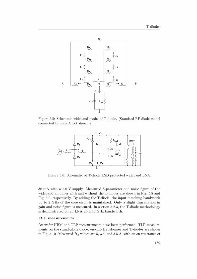
T-diodes
kL1 R11
R12R13R14
L12L13L14
Cp
L2R21R22R23R24
L22L23L24
CoxCsub Rsub
A BX
Figure 5.5: Schematic wideband model of T-diode. (Standard RF diode modelconnected to node X not shown.)
L1 L2D2D1 M1M2 M6Rload
M3M4M5
VDDIbias
RFinRFout
SCR
Figure 5.6: Schematic of T-diode ESD protected wideband LNA.
38 mA with a 1.8 V supply. Measured S-parameter and noise figure of thewideband amplifier with and without the T-diodes are shown in Fig. 5.8 andFig. 5.9, respectively. By adding the T-diode, the input matching bandwidthup to 2 GHz of the core ciruit is maintained. Only a slight degradation ingain and noise figure is measured. In section 5.2.3, the T-diode methodologyis demonstrated on an LNA with 16 GHz bandwidth.
ESD measurements
On-wafer HBM and TLP measurements have been performed. TLP measure-ments on the stand-alone diode, on-chip transformer and T-diodes are shownin Fig. 5.10. Measured It2 values are 5, 3.5, and 3.5 A, with an on-resistance of
189
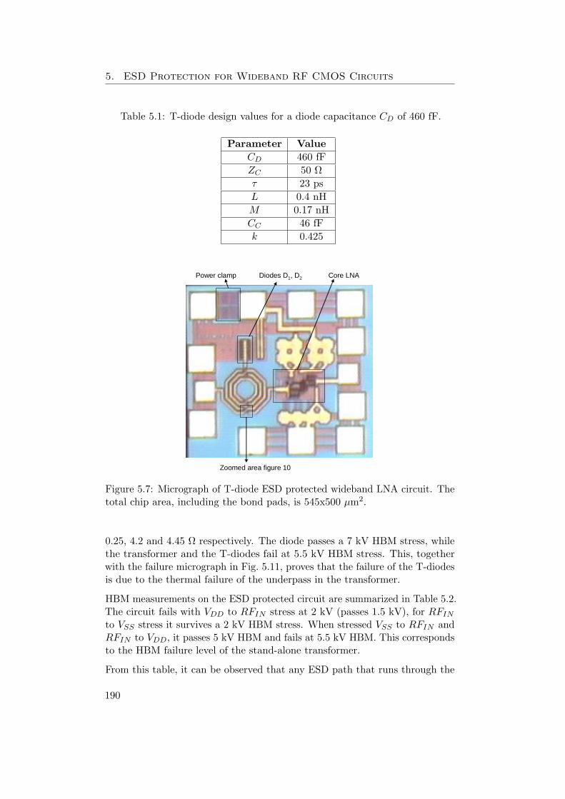
5. ESD Protection for Wideband RF CMOS Circuits
Table 5.1: T-diode design values for a diode capacitance CD of 460 fF.
Parameter ValueCD 460 fFZC 50 Ωτ 23 psL 0.4 nHM 0.17 nHCC 46 fFk 0.425
Diodes D1, D2 Core LNAPower clamp
Zoomed area figure 10
Figure 5.7: Micrograph of T-diode ESD protected wideband LNA circuit. Thetotal chip area, including the bond pads, is 545x500 µm2.
0.25, 4.2 and 4.45 Ω respectively. The diode passes a 7 kV HBM stress, whilethe transformer and the T-diodes fail at 5.5 kV HBM stress. This, togetherwith the failure micrograph in Fig. 5.11, proves that the failure of the T-diodesis due to the thermal failure of the underpass in the transformer.
HBM measurements on the ESD protected circuit are summarized in Table 5.2.The circuit fails with VDD to RFIN stress at 2 kV (passes 1.5 kV), for RFIN
to VSS stress it survives a 2 kV HBM stress. When stressed VSS to RFIN andRFIN to VDD, it passes 5 kV HBM and fails at 5.5 kV HBM. This correspondsto the HBM failure level of the stand-alone transformer.
From this table, it can be observed that any ESD path that runs through the
190
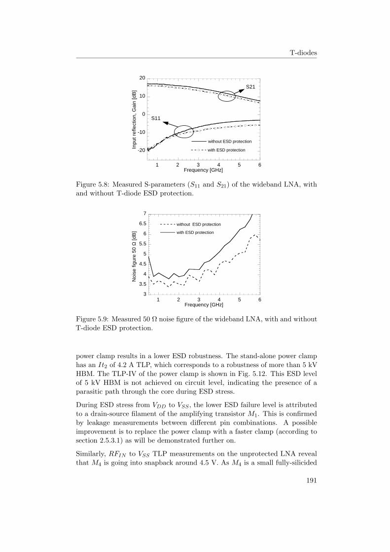
T-diodes
-20
-10
0
10
20
1 2 3 4 5 6
without ESD protection
with ESD protection
Inpu
t ref
lect
ion,
Gai
n [d
B]
Frequency [GHz]
S11
S21
Figure 5.8: Measured S-parameters (S11 and S21) of the wideband LNA, withand without T-diode ESD protection.
3
3.5
4
4.5
5
5.5
6
6.5
7
1 2 3 4 5 6
without ESD protection
with ESD protection
Noi
se fi
gure
50
Ω [d
B]
Frequency [GHz]
Figure 5.9: Measured 50 Ω noise figure of the wideband LNA, with and withoutT-diode ESD protection.
power clamp results in a lower ESD robustness. The stand-alone power clamphas an It2 of 4.2 A TLP, which corresponds to a robustness of more than 5 kVHBM. The TLP-IV of the power clamp is shown in Fig. 5.12. This ESD levelof 5 kV HBM is not achieved on circuit level, indicating the presence of aparasitic path through the core during ESD stress.
During ESD stress from VDD to VSS , the lower ESD failure level is attributedto a drain-source filament of the amplifying transistor M1. This is confirmedby leakage measurements between different pin combinations. A possibleimprovement is to replace the power clamp with a faster clamp (according tosection 2.5.3.1) as will be demonstrated further on.
Similarly, RFIN to VSS TLP measurements on the unprotected LNA revealthat M4 is going into snapback around 4.5 V. As M4 is a small fully-silicided
191
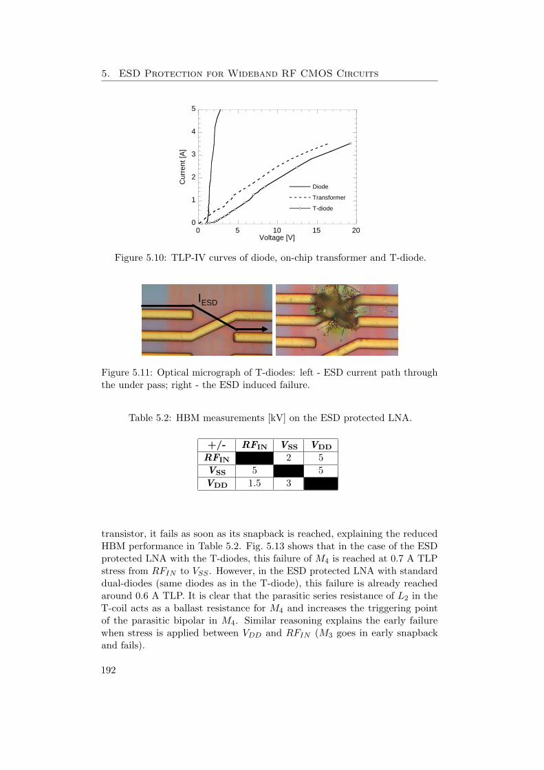
5. ESD Protection for Wideband RF CMOS Circuits
0
1
2
3
4
5
0 5 10 15 20
Diode
Transformer
T-diode
Cur
rent
[A]
Voltage [V]
Figure 5.10: TLP-IV curves of diode, on-chip transformer and T-diode.
IESD
Figure 5.11: Optical micrograph of T-diodes: left - ESD current path throughthe under pass; right - the ESD induced failure.
Table 5.2: HBM measurements [kV] on the ESD protected LNA.
+/- RFIN VSS VDD
RFIN 2 5VSS 5 5VDD 1.5 3
transistor, it fails as soon as its snapback is reached, explaining the reducedHBM performance in Table 5.2. Fig. 5.13 shows that in the case of the ESDprotected LNA with the T-diodes, this failure of M4 is reached at 0.7 A TLPstress from RFIN to VSS . However, in the ESD protected LNA with standarddual-diodes (same diodes as in the T-diode), this failure is already reachedaround 0.6 A TLP. It is clear that the parasitic series resistance of L2 in theT-coil acts as a ballast resistance for M4 and increases the triggering pointof the parasitic bipolar in M4. Similar reasoning explains the early failurewhen stress is applied between VDD and RFIN (M3 goes in early snapbackand fails).
192
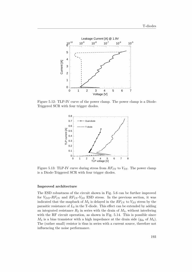
T-diodes
0
1
2
3
4
5
6
0 1 2 3 4 5 6 7
10-10 10-9 10-8 10-7 10-6 10-5
Cur
rent
[A]
Voltage [V]
Leakage Current [A] @ 1.9V
Figure 5.12: TLP-IV curve of the power clamp. The power clamp is a Diode-Triggered SCR with four trigger diodes.
0
0.1
0.2
0.3
0.4
0.5
0.6
0.7
0.8
0 1 2 3 4 5 6 7 8
Dual-diode
T-diode
TLP
cur
rent
[A]
TLP voltage [V]
Figure 5.13: TLP-IV curve during stress from RFIN to VSS . The power clampis a Diode-Triggered SCR with four trigger diodes.
Improved architecture
The ESD robustness of the circuit shown in Fig. 5.6 can be further improvedfor VDD-RFIN and RFIN -VSS ESD stress. In the previous section, it wasindicated that the snapback of M4 is delayed in the RFIN to VSS stress by theparasitic resistance of L2 in the T-diode. This effect can be extended by addingan integrated resistance R2 in series with the drain of M4, without interferingwith the RF circuit operation, as shown in Fig. 5.14. This is possible sinceM4 is a bias transistor with a high impedance at the drain side (gds of M4).The (rather small) resistor is thus in series with a current source, therefore notinfluencing the noise performance.
193
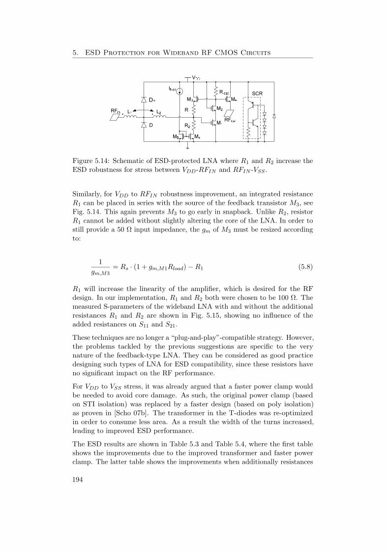
5. ESD Protection for Wideband RF CMOS Circuits
L1 L2D2D1 M1M2 M6Rload
M3M4M5
VDDIbias
RFinRFout
SCR
R1R2
Figure 5.14: Schematic of ESD-protected LNA where R1 and R2 increase theESD robustness for stress between VDD-RFIN and RFIN -VSS .
Similarly, for VDD to RFIN robustness improvement, an integrated resistanceR1 can be placed in series with the source of the feedback transistor M3, seeFig. 5.14. This again prevents M3 to go early in snapback. Unlike R2, resistorR1 cannot be added without slightly altering the core of the LNA. In order tostill provide a 50 Ω input impedance, the gm of M3 must be resized accordingto:
1gm,M3
= Rs · (1 + gm,M1Rload)−R1 (5.8)
R1 will increase the linearity of the amplifier, which is desired for the RFdesign. In our implementation, R1 and R2 both were chosen to be 100 Ω. Themeasured S-parameters of the wideband LNA with and without the additionalresistances R1 and R2 are shown in Fig. 5.15, showing no influence of theadded resistances on S11 and S21.
These techniques are no longer a “plug-and-play”-compatible strategy. However,the problems tackled by the previous suggestions are specific to the verynature of the feedback-type LNA. They can be considered as good practicedesigning such types of LNA for ESD compatibility, since these resistors haveno significant impact on the RF performance.
For VDD to VSS stress, it was already argued that a faster power clamp wouldbe needed to avoid core damage. As such, the original power clamp (basedon STI isolation) was replaced by a faster design (based on poly isolation)as proven in [Scho 07b]. The transformer in the T-diodes was re-optimizedin order to consume less area. As a result the width of the turns increased,leading to improved ESD performance.
The ESD results are shown in Table 5.3 and Table 5.4, where the first tableshows the improvements due to the improved transformer and faster powerclamp. The latter table shows the improvements when additionally resistances
194
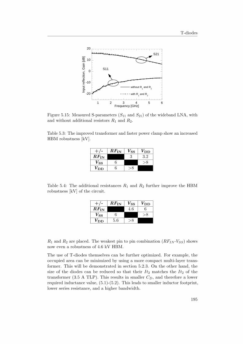
T-diodes
-20
-10
0
10
20
1 2 3 4 5 6
without R1 and R
2
with R1 and R
2
Inpu
t ref
lect
ion,
Gai
n [d
B]
Frequency [GHz]
S11
S21
Figure 5.15: Measured S-parameters (S11 and S21) of the wideband LNA, withand without additional resistors R1 and R2.
Table 5.3: The improved transformer and faster power clamp show an increasedHBM robustness [kV].
+/- RFIN VSS VDD
RFIN 3 3.2VSS 6 >8VDD 6 >8
Table 5.4: The additional resistances R1 and R2 further improve the HBMrobustness [kV] of the circuit.
+/- RFIN VSS VDD
RFIN 4.6 6VSS 6 >8VDD 5.6 >8
R1 and R2 are placed. The weakest pin to pin combination (RFIN -VSS) showsnow even a robustness of 4.6 kV HBM.
The use of T-diodes themselves can be further optimized. For example, theoccupied area can be minimized by using a more compact multi-layer trans-former. This will be demonstrated in section 5.2.3. On the other hand, thesize of the diodes can be reduced so that their It2 matches the It2 of thetransformer (3.5 A TLP). This results in smaller CD, and therefore a lowerrequired inductance value, (5.1)-(5.2). This leads to smaller inductor footprint,lower series resistance, and a higher bandwidth.
195
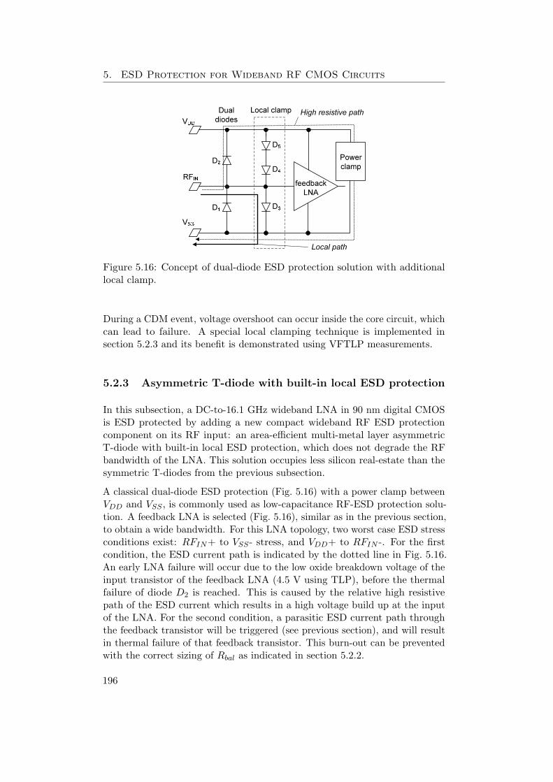
5. ESD Protection for Wideband RF CMOS Circuits
VDDRFINVSS
Local path
feedbackLNA
Powerclamp
High resistive path
D1D2
D3D4D5
Local clampDualdiodes
Figure 5.16: Concept of dual-diode ESD protection solution with additionallocal clamp.
During a CDM event, voltage overshoot can occur inside the core circuit, whichcan lead to failure. A special local clamping technique is implemented insection 5.2.3 and its benefit is demonstrated using VFTLP measurements.
5.2.3 Asymmetric T-diode with built-in local ESD protection
In this subsection, a DC-to-16.1 GHz wideband LNA in 90 nm digital CMOSis ESD protected by adding a new compact wideband RF ESD protectioncomponent on its RF input: an area-efficient multi-metal layer asymmetricT-diode with built-in local ESD protection, which does not degrade the RFbandwidth of the LNA. This solution occupies less silicon real-estate than thesymmetric T-diodes from the previous subsection.
A classical dual-diode ESD protection (Fig. 5.16) with a power clamp betweenVDD and VSS , is commonly used as low-capacitance RF-ESD protection solu-tion. A feedback LNA is selected (Fig. 5.16), similar as in the previous section,to obtain a wide bandwidth. For this LNA topology, two worst case ESD stressconditions exist: RFIN+ to VSS- stress, and VDD+ to RFIN -. For the firstcondition, the ESD current path is indicated by the dotted line in Fig. 5.16.An early LNA failure will occur due to the low oxide breakdown voltage of theinput transistor of the feedback LNA (4.5 V using TLP), before the thermalfailure of diode D2 is reached. This is caused by the relative high resistivepath of the ESD current which results in a high voltage build up at the inputof the LNA. For the second condition, a parasitic ESD current path throughthe feedback transistor will be triggered (see previous section), and will resultin thermal failure of that feedback transistor. This burn-out can be preventedwith the correct sizing of Rbal as indicated in section 5.2.2.
196
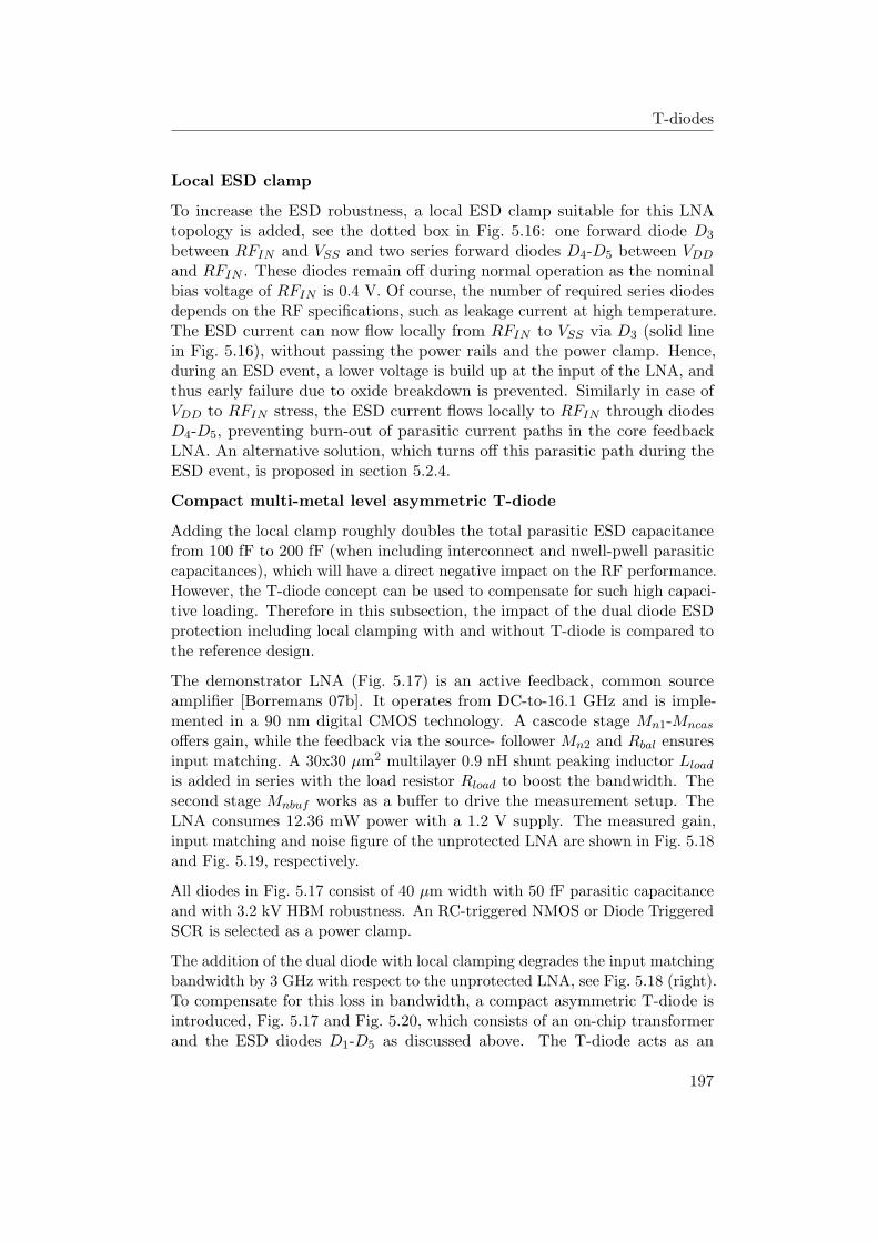
T-diodes
Local ESD clamp
To increase the ESD robustness, a local ESD clamp suitable for this LNAtopology is added, see the dotted box in Fig. 5.16: one forward diode D3
between RFIN and VSS and two series forward diodes D4-D5 between VDD
and RFIN . These diodes remain off during normal operation as the nominalbias voltage of RFIN is 0.4 V. Of course, the number of required series diodesdepends on the RF specifications, such as leakage current at high temperature.The ESD current can now flow locally from RFIN to VSS via D3 (solid linein Fig. 5.16), without passing the power rails and the power clamp. Hence,during an ESD event, a lower voltage is build up at the input of the LNA, andthus early failure due to oxide breakdown is prevented. Similarly in case ofVDD to RFIN stress, the ESD current flows locally to RFIN through diodesD4-D5, preventing burn-out of parasitic current paths in the core feedbackLNA. An alternative solution, which turns off this parasitic path during theESD event, is proposed in section 5.2.4.
Compact multi-metal level asymmetric T-diode
Adding the local clamp roughly doubles the total parasitic ESD capacitancefrom 100 fF to 200 fF (when including interconnect and nwell-pwell parasiticcapacitances), which will have a direct negative impact on the RF performance.However, the T-diode concept can be used to compensate for such high capaci-tive loading. Therefore in this subsection, the impact of the dual diode ESDprotection including local clamping with and without T-diode is compared tothe reference design.
The demonstrator LNA (Fig. 5.17) is an active feedback, common sourceamplifier [Borremans 07b]. It operates from DC-to-16.1 GHz and is imple-mented in a 90 nm digital CMOS technology. A cascode stage Mn1-Mncas
offers gain, while the feedback via the source- follower Mn2 and Rbal ensuresinput matching. A 30x30 µm2 multilayer 0.9 nH shunt peaking inductor Lload
is added in series with the load resistor Rload to boost the bandwidth. Thesecond stage Mnbuf works as a buffer to drive the measurement setup. TheLNA consumes 12.36 mW power with a 1.2 V supply. The measured gain,input matching and noise figure of the unprotected LNA are shown in Fig. 5.18and Fig. 5.19, respectively.
All diodes in Fig. 5.17 consist of 40 µm width with 50 fF parasitic capacitanceand with 3.2 kV HBM robustness. An RC-triggered NMOS or Diode TriggeredSCR is selected as a power clamp.
The addition of the dual diode with local clamping degrades the input matchingbandwidth by 3 GHz with respect to the unprotected LNA, see Fig. 5.18 (right).To compensate for this loss in bandwidth, a compact asymmetric T-diode isintroduced, Fig. 5.17 and Fig. 5.20, which consists of an on-chip transformerand the ESD diodes D1-D5 as discussed above. The T-diode acts as an
197
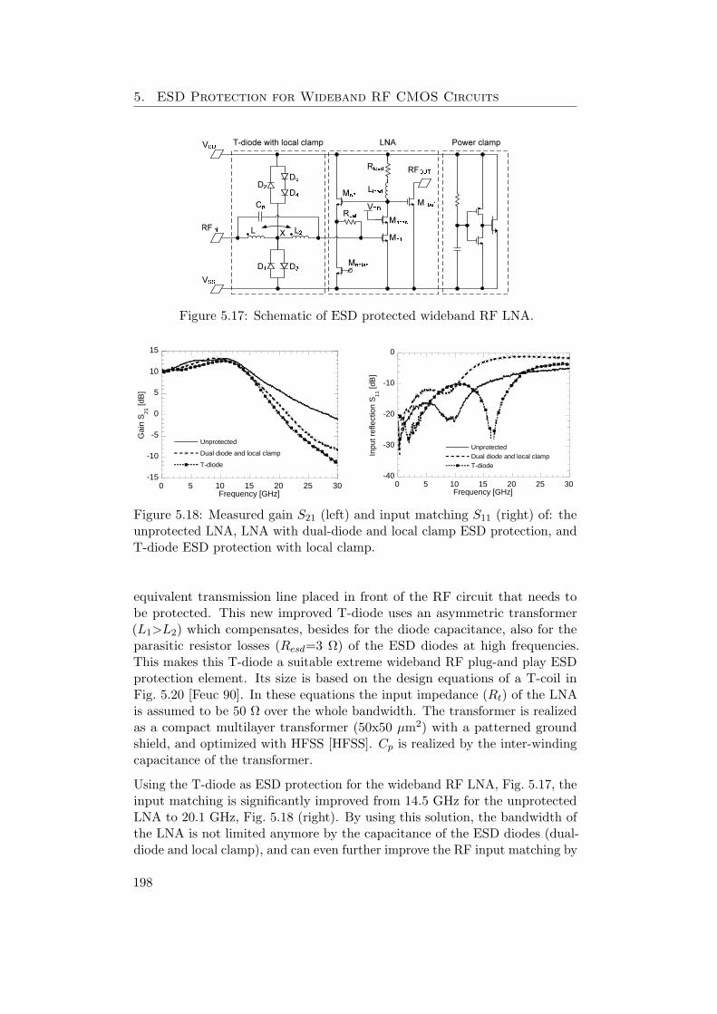
5. ESD Protection for Wideband RF CMOS Circuits
Mn1MncasLloadRload
Mn2Mnbias
MnbufVDDVDD
RFINVSS
RFOUTT-diode with local clamp
RbalL1 L2Cp
D5D2 D4
D1 D3
Power clamp
X
LNA
Figure 5.17: Schematic of ESD protected wideband RF LNA.
-15
-10
-5
0
5
10
15
0 5 10 15 20 25 30
Unprotected
Dual diode and local clamp
T-diode
Gai
n S
21 [d
B]
Frequency [GHz]
-40
-30
-20
-10
0
0 5 10 15 20 25 30
UnprotectedDual diode and local clampT-diode
Inpu
t ref
lect
ion
S11
[dB
]
Frequency [GHz]
Figure 5.18: Measured gain S21 (left) and input matching S11 (right) of: theunprotected LNA, LNA with dual-diode and local clamp ESD protection, andT-diode ESD protection with local clamp.
equivalent transmission line placed in front of the RF circuit that needs tobe protected. This new improved T-diode uses an asymmetric transformer(L1>L2) which compensates, besides for the diode capacitance, also for theparasitic resistor losses (Resd=3 Ω) of the ESD diodes at high frequencies.This makes this T-diode a suitable extreme wideband RF plug-and play ESDprotection element. Its size is based on the design equations of a T-coil inFig. 5.20 [Feuc 90]. In these equations the input impedance (Rt) of the LNAis assumed to be 50 Ω over the whole bandwidth. The transformer is realizedas a compact multilayer transformer (50x50 µm2) with a patterned groundshield, and optimized with HFSS [HFSS]. Cp is realized by the inter-windingcapacitance of the transformer.
Using the T-diode as ESD protection for the wideband RF LNA, Fig. 5.17, theinput matching is significantly improved from 14.5 GHz for the unprotectedLNA to 20.1 GHz, Fig. 5.18 (right). By using this solution, the bandwidth ofthe LNA is not limited anymore by the capacitance of the ESD diodes (dual-diode and local clamp), and can even further improve the RF input matching by
198
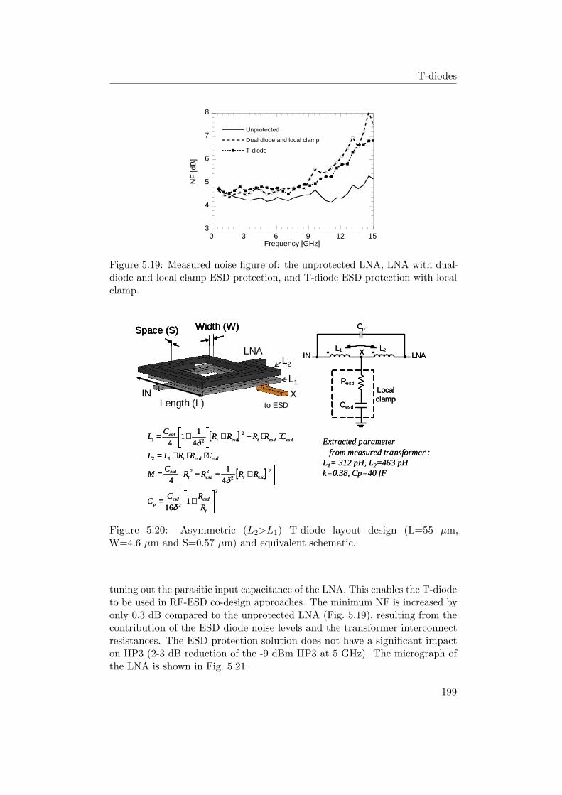
T-diodes
3
4
5
6
7
8
0 3 6 9 12 15
Unprotected
Dual diode and local clamp
T-diode
NF
[dB
]
Frequency [GHz]
Figure 5.19: Measured noise figure of: the unprotected LNA, LNA with dual-diode and local clamp ESD protection, and T-diode ESD protection with localclamp.
[ ]
[ ]2
2
2
222
12
2
21
116
4
1
4
4
11
4
+=
+−−=
⋅⋅+=
⋅⋅−+ +=
t
esdesdp
esdtesdtesd
esdesdt
esdesdtesdtesd
R
RCC
RRRRC
M
CRRLL
CRRRRC
L
δ
δ
δ Extracted parameter from measured transformer :
L1= 312 pH, L2=463 pHk=0.38, Cp=40 fF
INto ESD
LNA
Width (W)
Length (L)X
L2
L1
Space (S)
L1 L2
Resd
Cesd
Cp
LNAIN X
Local clamp
[ ]
[ ]2
2
2
222
12
2
21
116
4
1
4
4
11
4
+=
+−−=
⋅⋅+=
⋅⋅−+ +=
t
esdesdp
esdtesdtesd
esdesdt
esdesdtesdtesd
R
RCC
RRRRC
M
CRRLL
CRRRRC
L
δ
δ
δ Extracted parameter from measured transformer :
L1= 312 pH, L2=463 pHk=0.38, Cp=40 fF
INto ESD
LNA
Width (W)
Length (L)X
L2
L1
Space (S)
INto ESD
LNA
Width (W)
Length (L)X
L2
L1
Space (S)
L1 L2
Resd
Cesd
Cp
LNAIN X
Local clamp
Figure 5.20: Asymmetric (L2>L1) T-diode layout design (L=55 µm,W=4.6 µm and S=0.57 µm) and equivalent schematic.
tuning out the parasitic input capacitance of the LNA. This enables the T-diodeto be used in RF-ESD co-design approaches. The minimum NF is increased byonly 0.3 dB compared to the unprotected LNA (Fig. 5.19), resulting from thecontribution of the ESD diode noise levels and the transformer interconnectresistances. The ESD protection solution does not have a significant impacton IIP3 (2-3 dB reduction of the -9 dBm IIP3 at 5 GHz). The micrograph ofthe LNA is shown in Fig. 5.21.
199
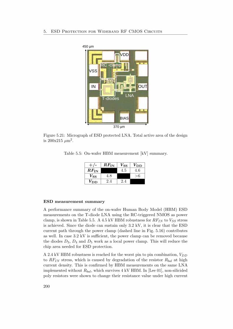
5. ESD Protection for Wideband RF CMOS Circuits
370 µm
450 µm
LNAT-diodes
In Out
RC -clamp
IN OUT
VDD
BIAS
VSS
Figure 5.21: Micrograph of ESD protected LNA. Total active area of the designis 200x215 µm2.
Table 5.5: On-wafer HBM measurement [kV] summary.
+/- RFIN VSS VDD
RFIN 4.5 4.6VSS 4.8 >6VDD 2.4 2.4
ESD measurement summary
A performance summary of the on-wafer Human Body Model (HBM) ESDmeasurements on the T-diode LNA using the RC-triggered NMOS as powerclamp, is shown in Table 5.5. A 4.5 kV HBM robustness for RFIN to VSS stressis achieved. Since the diode can sustain only 3.2 kV, it is clear that the ESDcurrent path through the power clamp (dashed line in Fig. 5.16) contributesas well. In case 3.2 kV is sufficient, the power clamp can be removed becausethe diodes D3, D4 and D5 work as a local power clamp. This will reduce thechip area needed for ESD protection.
A 2.4 kV HBM robustness is reached for the worst pin to pin combination, VDD
to RFIN stress, which is caused by degradation of the resistor Rbal at highcurrent density. This is confirmed by HBM measurements on the same LNAimplemented without Rbal, which survives 4 kV HBM. In [Lee 01], non-silicidedpoly resistors were shown to change their resistance value under high current
200
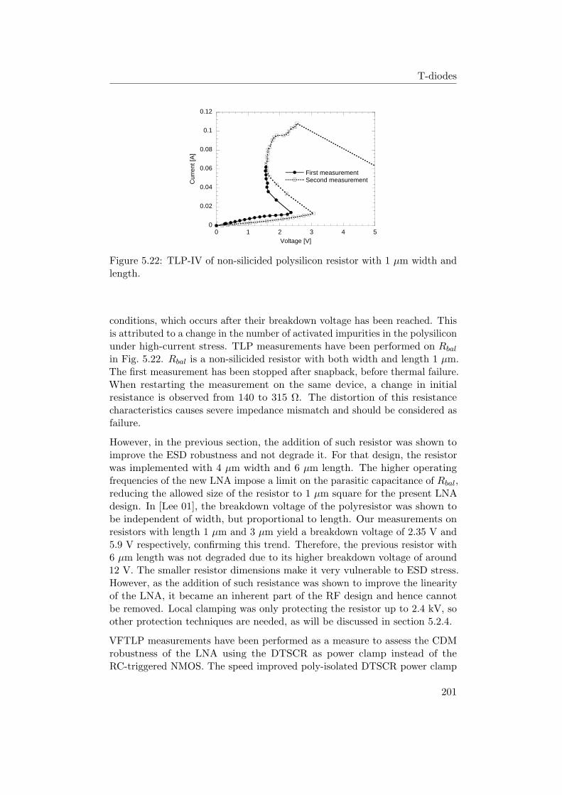
T-diodes
0
0.02
0.04
0.06
0.08
0.1
0.12
0 1 2 3 4 5
First measurementSecond measurementC
urre
nt [A
]
Voltage [V]
Figure 5.22: TLP-IV of non-silicided polysilicon resistor with 1 µm width andlength.
conditions, which occurs after their breakdown voltage has been reached. Thisis attributed to a change in the number of activated impurities in the polysiliconunder high-current stress. TLP measurements have been performed on Rbal
in Fig. 5.22. Rbal is a non-silicided resistor with both width and length 1 µm.The first measurement has been stopped after snapback, before thermal failure.When restarting the measurement on the same device, a change in initialresistance is observed from 140 to 315 Ω. The distortion of this resistancecharacteristics causes severe impedance mismatch and should be considered asfailure.
However, in the previous section, the addition of such resistor was shown toimprove the ESD robustness and not degrade it. For that design, the resistorwas implemented with 4 µm width and 6 µm length. The higher operatingfrequencies of the new LNA impose a limit on the parasitic capacitance of Rbal,reducing the allowed size of the resistor to 1 µm square for the present LNAdesign. In [Lee 01], the breakdown voltage of the polyresistor was shown tobe independent of width, but proportional to length. Our measurements onresistors with length 1 µm and 3 µm yield a breakdown voltage of 2.35 V and5.9 V respectively, confirming this trend. Therefore, the previous resistor with6 µm length was not degraded due to its higher breakdown voltage of around12 V. The smaller resistor dimensions make it very vulnerable to ESD stress.However, as the addition of such resistance was shown to improve the linearityof the LNA, it became an inherent part of the RF design and hence cannotbe removed. Local clamping was only protecting the resistor up to 2.4 kV, soother protection techniques are needed, as will be discussed in section 5.2.4.
VFTLP measurements have been performed as a measure to assess the CDMrobustness of the LNA using the DTSCR as power clamp instead of theRC-triggered NMOS. The speed improved poly-isolated DTSCR power clamp
201
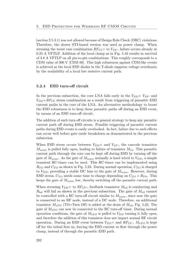
5. ESD Protection for Wideband RF CMOS Circuits
(section 2.5.3.1) was not allowed because of Design Rule Check (DRC) violations.Therefore, the slower STI-based version was used as power clamp. Whenstressing the worst case combination RFIN+ to VSS-, failure occurs already at0.25 A VFTLP. Addition of the local clamp as in Fig. 5.16 results in survivalof 3.8 A VFTLP on all pin-to-pin combinations. This roughly corresponds to aCDM value of 300 V [CDM 08]. This high robustness against CDM-like eventsis achieved as the local ESD diodes in the T-diode suppress voltage overshoots,by the availability of a local low resistive current path.
5.2.4 ESD turn-off circuit
In the previous subsection, the core LNA fails early in the VDD+ VSS- andVDD+RFIN stress combination as a result from triggering of parasitic ESDcurrent paths in the core of the LNA. An alternative methodology to boostthe ESD robustness is to keep these parasitic paths off during an ESD event,by means of an ESD turn-off circuit.
The addition of such turn-off circuits is a general strategy to keep any parasiticcurrent path off during ESD stress. Possible triggering of parasitic currentpaths during ESD events is easily overlooked. In fact, failure due to such effectscan occur well before gate oxide breakdown as demonstrated in the previoussubsection.
When ESD stress occurs between VDD+ and VSS-, the cascode transistorMncasc is pulled fully open, leading to failure of transistor Mn1. This parasiticcurrent path through the core can be kept off during ESD by turning off thegate of Mncasc. As the gate of Mncasc normally is hard wired to VDD, a simpletransient RC-timer can be used. This RC-timer can be implemented usingRTO and CTO as shown in Fig. 5.23. During normal operation, CTO is chargedto VDD, providing a stable DC bias to the gate of Mncasc. However, duringESD stress, CTO needs some time to charge depending on CTO ∗ RTO. Thiskeeps the gate of Mncasc low, thereby switching off the parasitic current path.
When stressing VDD+ to RFIN -, feedback transistor Mn2 is conducting andRbal will fail as shown in the previous subsection. The gate of Mn2 cannotbe controlled with a RC turn-off circuit similar to Mncasc, since now the gateis connected to an RF node, instead of a DC node. Therefore, an additionaltransistor MnTO (TO=Turn Off) is added at the drain of Mn2, Fig. 5.23. Thegate of MnTO can now be connected to the RC turn-off timer. During normaloperation conditions, the gate of MnTO is pulled to VDD turning it fully open,and therefore the addition of this transistor does not impact normal RF circuitoperation. During an ESD event between VDD+ and RFIN -, MnTO is keptoff for the initial first ns, forcing the ESD current to flow through the powerclamp, instead of through the parasitic ESD path.
202
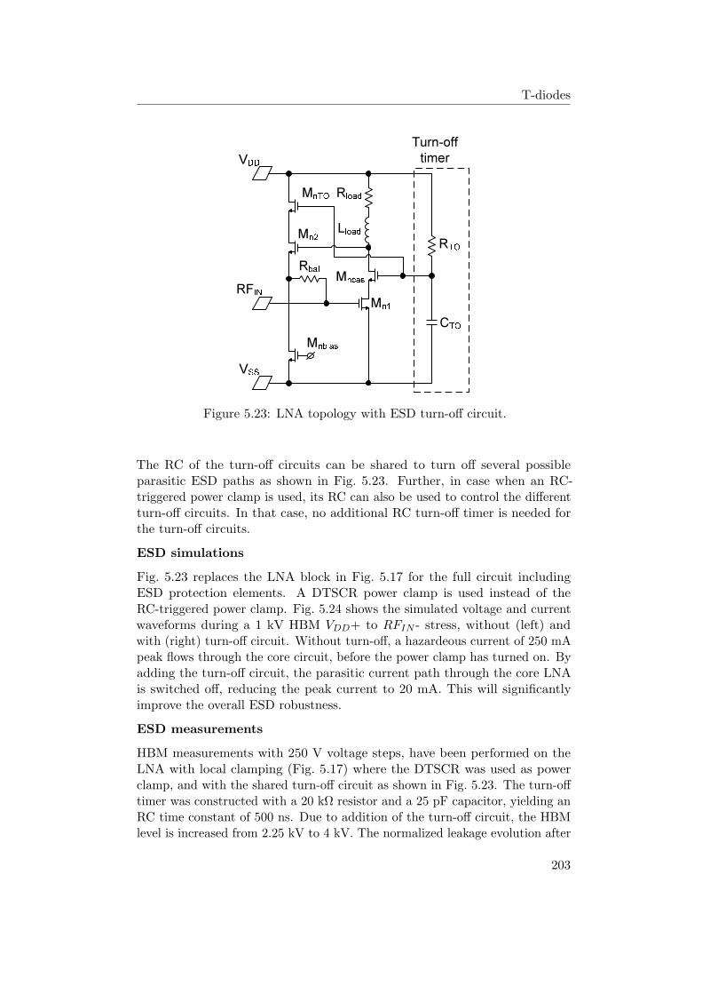
T-diodes
Mn1LloadRload
Mn2Mnbias
Rbal
Turn-offtimer
MncasMnTO
RTOCTO
VSSRFIN
VDD
Figure 5.23: LNA topology with ESD turn-off circuit.
The RC of the turn-off circuits can be shared to turn off several possibleparasitic ESD paths as shown in Fig. 5.23. Further, in case when an RC-triggered power clamp is used, its RC can also be used to control the differentturn-off circuits. In that case, no additional RC turn-off timer is needed forthe turn-off circuits.
ESD simulations
Fig. 5.23 replaces the LNA block in Fig. 5.17 for the full circuit includingESD protection elements. A DTSCR power clamp is used instead of theRC-triggered power clamp. Fig. 5.24 shows the simulated voltage and currentwaveforms during a 1 kV HBM VDD+ to RFIN - stress, without (left) andwith (right) turn-off circuit. Without turn-off, a hazardeous current of 250 mApeak flows through the core circuit, before the power clamp has turned on. Byadding the turn-off circuit, the parasitic current path through the core LNAis switched off, reducing the peak current to 20 mA. This will significantlyimprove the overall ESD robustness.
ESD measurements
HBM measurements with 250 V voltage steps, have been performed on theLNA with local clamping (Fig. 5.17) where the DTSCR was used as powerclamp, and with the shared turn-off circuit as shown in Fig. 5.23. The turn-offtimer was constructed with a 20 kΩ resistor and a 25 pF capacitor, yielding anRC time constant of 500 ns. Due to addition of the turn-off circuit, the HBMlevel is increased from 2.25 kV to 4 kV. The normalized leakage evolution after
203
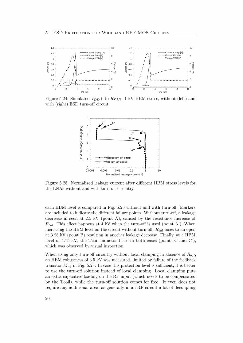
5. ESD Protection for Wideband RF CMOS Circuits
0
0.2
0.4
0.6
0.8
1
1.2
1.4
0
2
4
6
8
10
0 2 4 6 8 10
Current Clamp [A]Current Core [A]Voltage VDD [V]
Cur
rent
[A
] Voltage [V
]
Time [ns]
0
0.2
0.4
0.6
0.8
1
1.2
1.4
0
2
4
6
8
10
0 2 4 6 8 10
Current Clamp [A]Current Core [A]Voltage VDD [V]
Cur
rent
[A
] Voltage [V
]
Time [ns]
Figure 5.24: Simulated VDD+ to RFIN - 1 kV HBM stress, without (left) andwith (right) ESD turn-off circuit.
0
1
2
3
4
5
6
0.0001 0.001 0.01 0.1 1 10
Without turn-off circuit
With turn-off circuit
HB
M p
rech
arge
vol
tage
[kV
]
Normalized leakage current [-]
A
B
A'
C'C
Figure 5.25: Normalized leakage current after different HBM stress levels forthe LNAs without and with turn-off circuitry.
each HBM level is compared in Fig. 5.25 without and with turn-off. Markersare included to indicate the different failure points. Without turn-off, a leakagedecrease in seen at 2.5 kV (point A), caused by the resistance increase ofRbal. This effect happens at 4 kV when the turn-off is used (point A’). Whenincreasing the HBM level on the circuit without turn-off, Rbal fuses to an openat 3.25 kV (point B) resulting in another leakage decrease. Finally, at a HBMlevel of 4.75 kV, the Tcoil inductor fuses in both cases (points C and C’),which was observed by visual inspection.
When using only turn-off circuitry without local clamping in absence of Rbal,an HBM robustness of 3.5 kV was measured, limited by failure of the feedbacktransitor Mn2 in Fig. 5.23. In case this protection level is sufficient, it is betterto use the turn-off solution instead of local clamping. Local clamping putsan extra capacitive loading on the RF input (which needs to be compensatedby the Tcoil), while the turn-off solution comes for free. It even does notrequire any additional area, as generally in an RF circuit a lot of decoupling
204
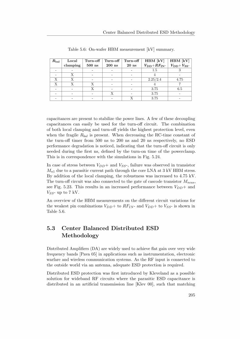
Center Balanced Distributed ESD Methodology
Table 5.6: On-wafer HBM measurement [kV] summary.
Rbal Local Turn-off Turn-off Turn-off HBM [kV] HBM [kV]clamping 500 ns 200 ns 20 ns VDD+RFIN- VDD+VSS-
- - - - - 1.5 3- X - - - 4 -X X - - - 2.25/2.4 4.75X X X - - 4 7- - X - - 3.75 6.5- - - X - 3.75 -- - - - X 3.75 -
capacitances are present to stabilize the power lines. A few of these decouplingcapacitances can easily be used for the turn-off circuit. The combinationof both local clamping and turn-off yields the highest protection level, evenwhen the fragile Rbal is present. When decreasing the RC-time constant ofthe turn-off timer from 500 ns to 200 ns and 20 ns respectively, no ESDperformance degradation is noticed, indicating that the turn-off circuit is onlyneeded during the first ns, defined by the turn-on time of the powerclamp.This is in correspondence with the simulations in Fig. 5.24.
In case of stress between VDD+ and VSS-, failure was observed in transistorMn1 due to a parasitic current path through the core LNA at 3 kV HBM stress.By addition of the local clamping, the robustness was increased to 4.75 kV.The turn-off circuit was also connected to the gate of cascode transistor Mncas,see Fig. 5.23. This results in an increased performance between VDD+ andVSS- up to 7 kV.
An overview of the HBM measurements on the different circuit variations forthe weakest pin combinations VDD+ to RFIN - and VDD+ to VSS- is shown inTable 5.6.
5.3 Center Balanced Distributed ESDMethodology
Distributed Amplifiers (DA) are widely used to achieve flat gain over very widefrequency bands [Pava 05] in applications such as instrumentation, electronicwarfare and wireless communication systems. As the RF input is connected tothe outside world via an antenna, adequate ESD protection is required.
Distributed ESD protection was first introduced by Kleveland as a possiblesolution for wideband RF circuits where the parasitic ESD capacitance isdistributed in an artificial transmission line [Klev 00], such that matching
205
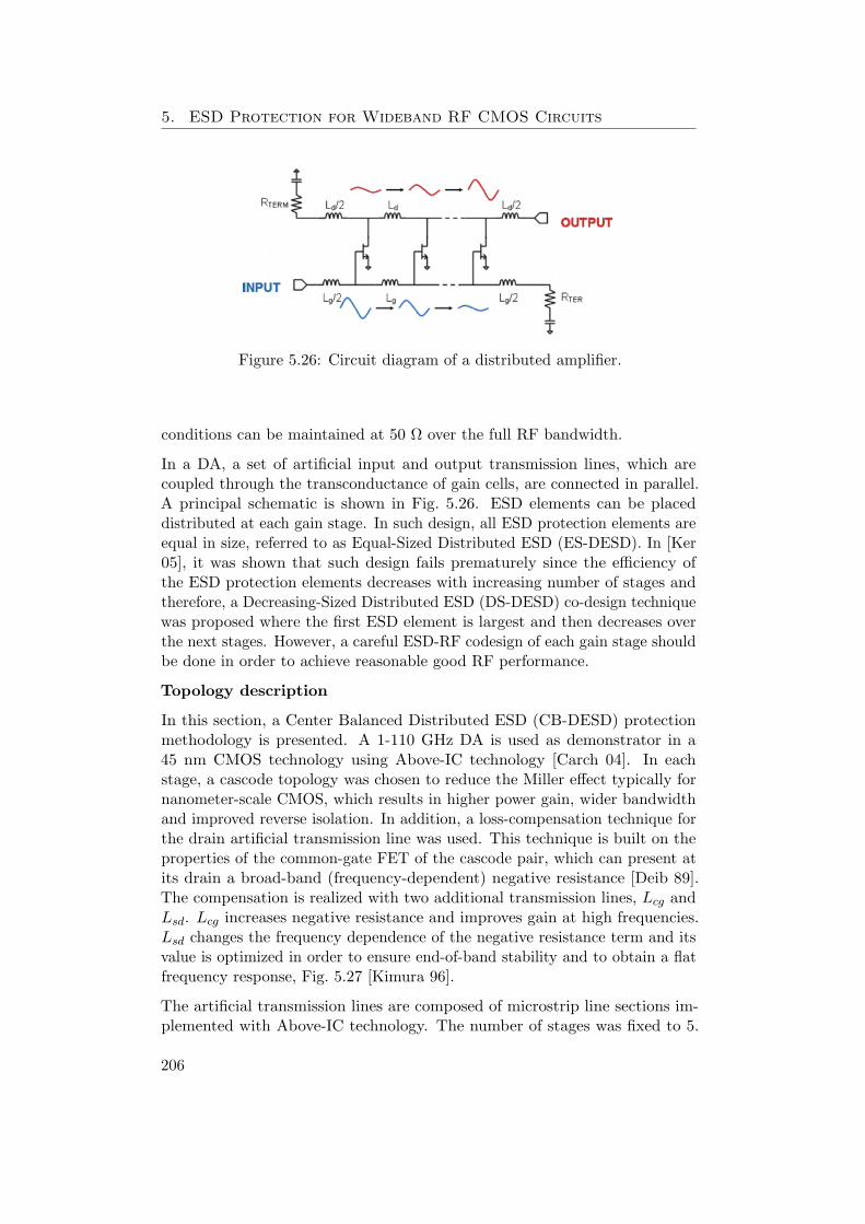
5. ESD Protection for Wideband RF CMOS Circuits
Figure 5.26: Circuit diagram of a distributed amplifier.
conditions can be maintained at 50 Ω over the full RF bandwidth.
In a DA, a set of artificial input and output transmission lines, which arecoupled through the transconductance of gain cells, are connected in parallel.A principal schematic is shown in Fig. 5.26. ESD elements can be placeddistributed at each gain stage. In such design, all ESD protection elements areequal in size, referred to as Equal-Sized Distributed ESD (ES-DESD). In [Ker05], it was shown that such design fails prematurely since the efficiency ofthe ESD protection elements decreases with increasing number of stages andtherefore, a Decreasing-Sized Distributed ESD (DS-DESD) co-design techniquewas proposed where the first ESD element is largest and then decreases overthe next stages. However, a careful ESD-RF codesign of each gain stage shouldbe done in order to achieve reasonable good RF performance.
Topology description
In this section, a Center Balanced Distributed ESD (CB-DESD) protectionmethodology is presented. A 1-110 GHz DA is used as demonstrator in a45 nm CMOS technology using Above-IC technology [Carch 04]. In eachstage, a cascode topology was chosen to reduce the Miller effect typically fornanometer-scale CMOS, which results in higher power gain, wider bandwidthand improved reverse isolation. In addition, a loss-compensation technique forthe drain artificial transmission line was used. This technique is built on theproperties of the common-gate FET of the cascode pair, which can present atits drain a broad-band (frequency-dependent) negative resistance [Deib 89].The compensation is realized with two additional transmission lines, Lcg andLsd. Lcg increases negative resistance and improves gain at high frequencies.Lsd changes the frequency dependence of the negative resistance term and itsvalue is optimized in order to ensure end-of-band stability and to obtain a flatfrequency response, Fig. 5.27 [Kimura 96].
The artificial transmission lines are composed of microstrip line sections im-plemented with Above-IC technology. The number of stages was fixed to 5.
206
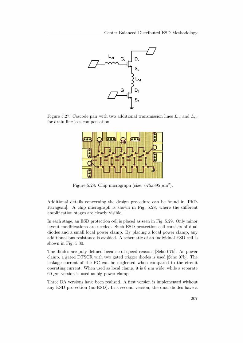
Center Balanced Distributed ESD Methodology
LcgLsd
G1 D1S1
G2 D2S2
Figure 5.27: Cascode pair with two additional transmission lines Lcg and Lsd
for drain line loss compensation.
Figure 5.28: Chip micrograph (size: 675x395 µm2).
Additional details concerning the design procedure can be found in [PhD-Pavageau]. A chip micrograph is shown in Fig. 5.28, where the differentamplification stages are clearly visible.
In each stage, an ESD protection cell is placed as seen in Fig. 5.29. Only minorlayout modifications are needed. Such ESD protection cell consists of dualdiodes and a small local power clamp. By placing a local power clamp, anyadditional bus resistance is avoided. A schematic of an individual ESD cell isshown in Fig. 5.30.
The diodes are poly-defined because of speed reasons [Scho 07b]. As powerclamp, a gated DTSCR with two gated trigger diodes is used [Scho 07b]. Theleakage current of the PC can be neglected when compared to the circuitoperating current. When used as local clamp, it is 8 µm wide, while a separate60 µm version is used as big power clamp.
Three DA versions have been realized. A first version is implemented withoutany ESD protection (no-ESD). In a second version, the dual diodes have a
207
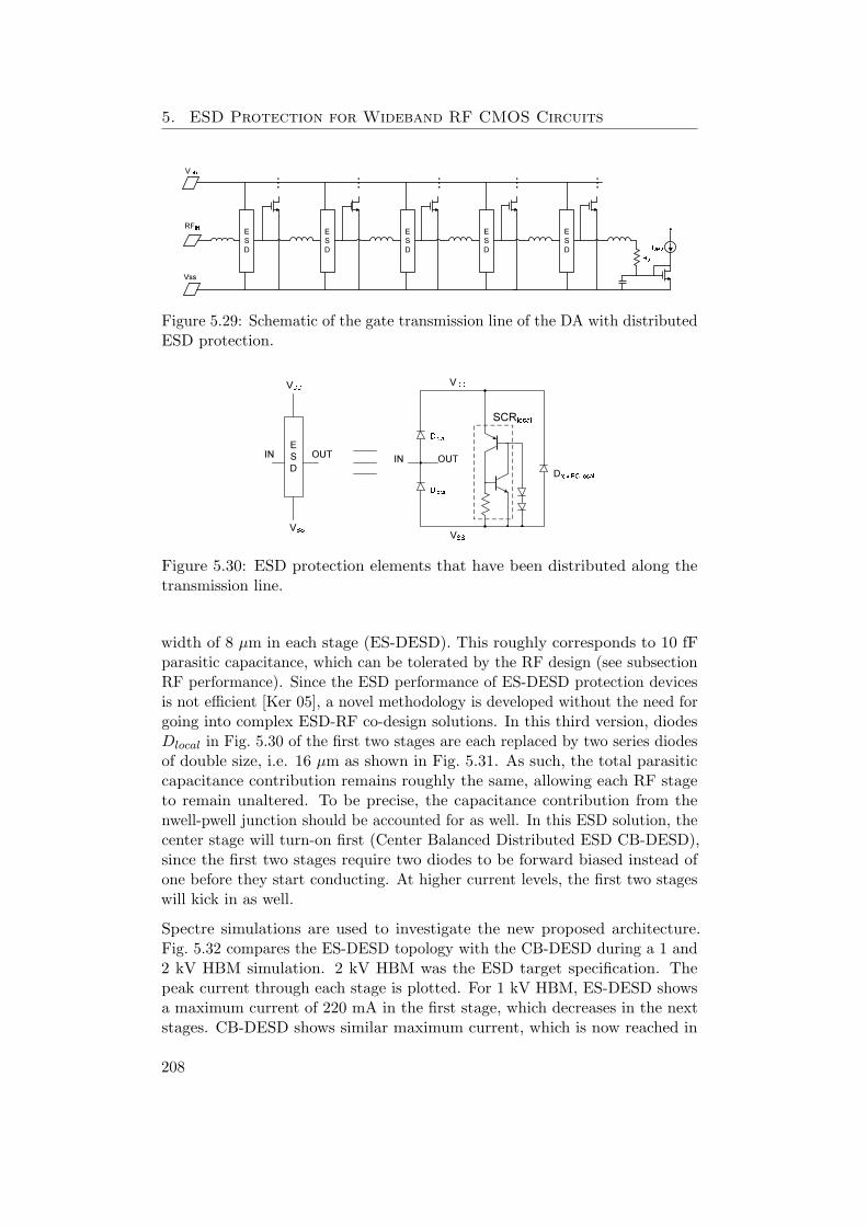
5. ESD Protection for Wideband RF CMOS Circuits
RFINVss
VDDRS IBIASE
SD
ESD
ESD
ESD
ESD
...
...
...
...
...
Figure 5.29: Schematic of the gate transmission line of the DA with distributedESD protection.
ESD
VSS
VDDSCRlocal
Drev,PC,localIN OUT
VDD
VSSDlocalDlocalIN OUT
Figure 5.30: ESD protection elements that have been distributed along thetransmission line.
width of 8 µm in each stage (ES-DESD). This roughly corresponds to 10 fFparasitic capacitance, which can be tolerated by the RF design (see subsectionRF performance). Since the ESD performance of ES-DESD protection devicesis not efficient [Ker 05], a novel methodology is developed without the need forgoing into complex ESD-RF co-design solutions. In this third version, diodesDlocal in Fig. 5.30 of the first two stages are each replaced by two series diodesof double size, i.e. 16 µm as shown in Fig. 5.31. As such, the total parasiticcapacitance contribution remains roughly the same, allowing each RF stageto remain unaltered. To be precise, the capacitance contribution from thenwell-pwell junction should be accounted for as well. In this ESD solution, thecenter stage will turn-on first (Center Balanced Distributed ESD CB-DESD),since the first two stages require two diodes to be forward biased instead ofone before they start conducting. At higher current levels, the first two stageswill kick in as well.
Spectre simulations are used to investigate the new proposed architecture.Fig. 5.32 compares the ES-DESD topology with the CB-DESD during a 1 and2 kV HBM simulation. 2 kV HBM was the ESD target specification. Thepeak current through each stage is plotted. For 1 kV HBM, ES-DESD showsa maximum current of 220 mA in the first stage, which decreases in the nextstages. CB-DESD shows similar maximum current, which is now reached in
208
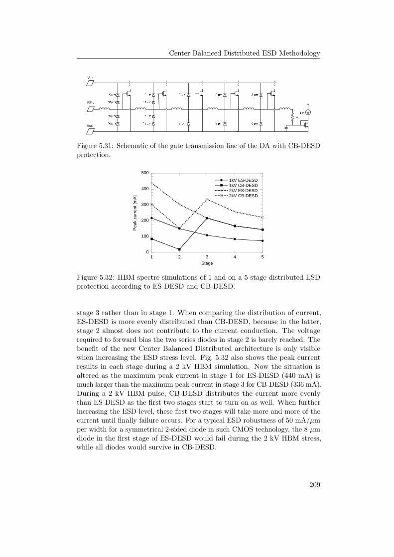
Center Balanced Distributed ESD Methodology
RFINVss
VDDRS IBIAS
...
...
...
...
...16 µm16 µm16 µm16 µm
16 µm16 µm16 µm16 µm8 µm8 µm
8 µm8 µm
8 µm8 µm
Figure 5.31: Schematic of the gate transmission line of the DA with CB-DESDprotection.
0
100
200
300
400
500
1 2 3 4 5
1kV ES-DESD1kV CB-DESD2kV ES-DESD2kV CB-DESD
Pea
k cu
rren
t [m
A]
Stage
Figure 5.32: HBM spectre simulations of 1 and on a 5 stage distributed ESDprotection according to ES-DESD and CB-DESD.
stage 3 rather than in stage 1. When comparing the distribution of current,ES-DESD is more evenly distributed than CB-DESD, because in the latter,stage 2 almost does not contribute to the current conduction. The voltagerequired to forward bias the two series diodes in stage 2 is barely reached. Thebenefit of the new Center Balanced Distributed architecture is only visiblewhen increasing the ESD stress level. Fig. 5.32 also shows the peak currentresults in each stage during a 2 kV HBM simulation. Now the situation isaltered as the maximum peak current in stage 1 for ES-DESD (440 mA) ismuch larger than the maximum peak current in stage 3 for CB-DESD (336 mA).During a 2 kV HBM pulse, CB-DESD distributes the current more evenlythan ES-DESD as the first two stages start to turn on as well. When furtherincreasing the ESD level, these first two stages will take more and more of thecurrent until finally failure occurs. For a typical ESD robustness of 50 mA/µmper width for a symmetrical 2-sided diode in such CMOS technology, the 8 µmdiode in the first stage of ES-DESD would fail during the 2 kV HBM stress,while all diodes would survive in CB-DESD.
209
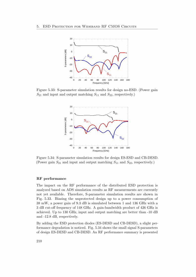
5. ESD Protection for Wideband RF CMOS Circuits
S11
S22
S21
-40
-30
-20
-10
0
10
20
0 20 40 60 80 100 120 140 160 180
S-p
aram
ete
rs [d
B]
Frequency [GHz]
Figure 5.33: S-parameter simulation results for design no-ESD. (Power gainS21 and input and output matching S11 and S22, respectively.)
S11
S22
S21
-40
-30
-20
-10
0
10
20
0 20 40 60 80 100 120 140 160 180
S-p
ara
met
ers
[dB
]
Frequency [GHz]
Figure 5.34: S-parameter simulation results for design ES-ESD and CB-DESD.(Power gain S21 and input and output matching S11 and S22, respectively.)
RF performance
The impact on the RF performance of the distributed ESD protection isanalyzed based on ADS simulation results as RF measurements are currentlynot yet available. Therefore, S-parameter simulation results are shown inFig. 5.33. Biasing the unprotected design up to a power consumption of38 mW, a power gain of 9.3 dB is simulated between 1 and 136 GHz with a3 dB cut-off frequency of 148 GHz. A gain-bandwidth product of 426 GHz isachieved. Up to 130 GHz, input and output matching are better than -10 dBand -12.8 dB, respectively.
By adding the ESD protection diodes (ES-DESD and CB-DESD), a slight per-formance degradation is noticed. Fig. 5.34 shows the small signal S-parametersof design ES-DESD and CB-DESD. An RF performance summary is presented
210
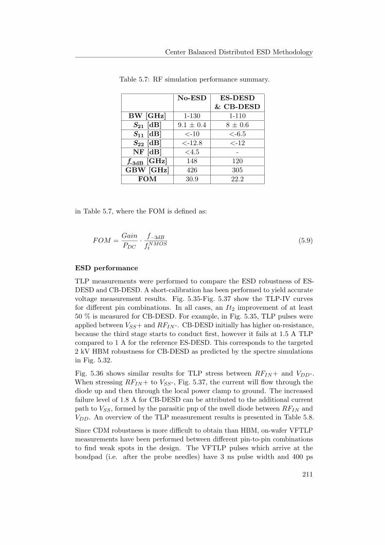
Center Balanced Distributed ESD Methodology
Table 5.7: RF simulation performance summary.
No-ESD ES-DESD& CB-DESD
BW [GHz] 1-130 1-110S21 [dB] 9.1 ± 0.4 8 ± 0.6S11 [dB] <-10 <-6.5S22 [dB] <-12.8 <-12NF [dB] <4.5 -
f-3dB [GHz] 148 120GBW [GHz] 426 305
FOM 30.9 22.2
in Table 5.7, where the FOM is defined as:
FOM =Gain
PDC· f−3dB
fNMOSt
(5.9)
ESD performance
TLP measurements were performed to compare the ESD robustness of ES-DESD and CB-DESD. A short-calibration has been performed to yield accuratevoltage measurement results. Fig. 5.35-Fig. 5.37 show the TLP-IV curvesfor different pin combinations. In all cases, an It2 improvement of at least50 % is measured for CB-DESD. For example, in Fig. 5.35, TLP pulses wereapplied between VSS+ and RFIN -. CB-DESD initially has higher on-resistance,because the third stage starts to conduct first, however it fails at 1.5 A TLPcompared to 1 A for the reference ES-DESD. This corresponds to the targeted2 kV HBM robustness for CB-DESD as predicted by the spectre simulationsin Fig. 5.32.
Fig. 5.36 shows similar results for TLP stress between RFIN+ and VDD-.When stressing RFIN+ to VSS-, Fig. 5.37, the current will flow through thediode up and then through the local power clamp to ground. The increasedfailure level of 1.8 A for CB-DESD can be attributed to the additional currentpath to VSS , formed by the parasitic pnp of the nwell diode between RFIN andVDD. An overview of the TLP measurement results is presented in Table 5.8.
Since CDM robustness is more difficult to obtain than HBM, on-wafer VFTLPmeasurements have been performed between different pin-to-pin combinationsto find weak spots in the design. The VFTLP pulses which arrive at thebondpad (i.e. after the probe needles) have 3 ns pulse width and 400 ps
211
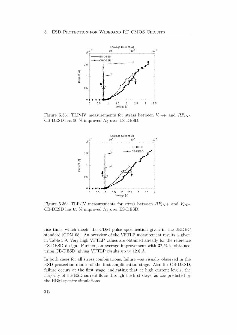
5. ESD Protection for Wideband RF CMOS Circuits
0
0.5
1
1.5
2
0 0.5 1 1.5 2 2.5 3 3.5
10-8 10-7 10-6 10-5
CB-DESD
ES-DESD
Cur
rent
[A]
Voltage [V]
Leakage Current [A]
Figure 5.35: TLP-IV measurements for stress between VSS+ and RFIN -.CB-DESD has 50 % improved It2 over ES-DESD.
0
0.5
1
1.5
2
0 0.5 1 1.5 2 2.5 3 3.5 4
10-7 10-6 10-5 10-4
CB-DESD
ES-DESD
Cur
rent
[A]
Voltage [V]
Leakage Current [A]
Figure 5.36: TLP-IV measurements for stress between RFIN+ and VDD-.CB-DESD has 65 % improved It2 over ES-DESD.
rise time, which meets the CDM pulse specification given in the JEDECstandard [CDM 08]. An overview of the VFTLP measurement results is givenin Table 5.9. Very high VFTLP values are obtained already for the referenceES-DESD design. Further, an average improvement with 32 % is obtainedusing CB-DESD, giving VFTLP results up to 12.8 A.
In both cases for all stress combinations, failure was visually observed in theESD protection diodes of the first amplification stage. Also for CB-DESD,failure occurs at the first stage, indicating that at high current levels, themajority of the ESD current flows through the first stage, as was predicted bythe HBM spectre simulations.
212
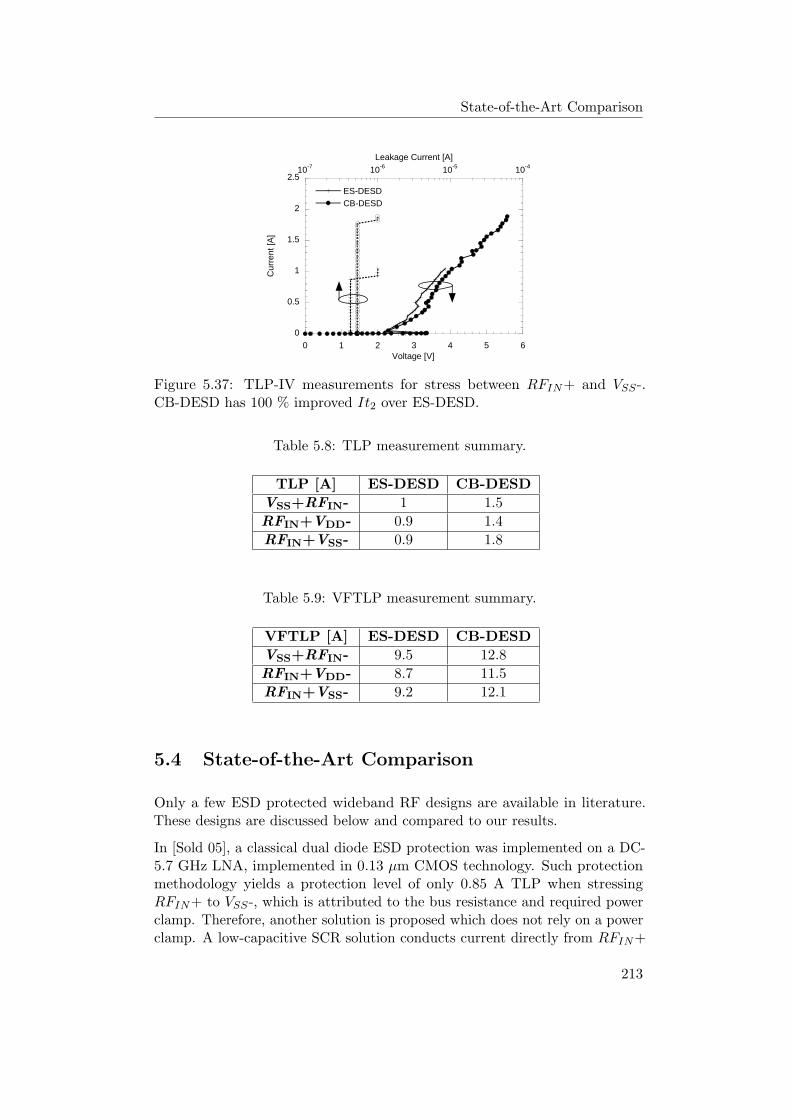
State-of-the-Art Comparison
0
0.5
1
1.5
2
2.5
0 1 2 3 4 5 6
10-7 10-6 10-5 10-4
CB-DESDES-DESD
Cur
rent
[A]
Voltage [V]
Leakage Current [A]
Figure 5.37: TLP-IV measurements for stress between RFIN+ and VSS-.CB-DESD has 100 % improved It2 over ES-DESD.
Table 5.8: TLP measurement summary.
TLP [A] ES-DESD CB-DESDVSS+RFIN- 1 1.5RFIN+VDD- 0.9 1.4RFIN+VSS- 0.9 1.8
Table 5.9: VFTLP measurement summary.
VFTLP [A] ES-DESD CB-DESDVSS+RFIN- 9.5 12.8RFIN+VDD- 8.7 11.5RFIN+VSS- 9.2 12.1
5.4 State-of-the-Art Comparison
Only a few ESD protected wideband RF designs are available in literature.These designs are discussed below and compared to our results.
In [Sold 05], a classical dual diode ESD protection was implemented on a DC-5.7 GHz LNA, implemented in 0.13 µm CMOS technology. Such protectionmethodology yields a protection level of only 0.85 A TLP when stressingRFIN+ to VSS-, which is attributed to the bus resistance and required powerclamp. Therefore, another solution is proposed which does not rely on a powerclamp. A low-capacitive SCR solution conducts current directly from RFIN+
213
5. ESD Protection for Wideband RF CMOS Circuits
to VSS-, improving the ESD robustness up to 3 kV HBM. A common-gateimplementation achieves a robustness of 5 kV. Since there is no decouplingcapacitor at the RF input, any overshoot generated by the SCR is directlyvisible at the gate oxide of the core transistor. Therefore, such methodologyshould be carefully investigated in more advanced technologies under CDMstress conditions to prove its applicability. The main conclusion from thispaper is that above 5 GHz, alternative ESD protection approaches will berequired.
The limitations of the classical dual diode protection become clearly visiblein [Borremans 07b], where they are used to protect a DC-6 GHz inductorlessfeedback LNA, implemented in 90 nm digital CMOS. A robustness of 3.2 kVHBM is measured between RFIN+ to VDD- and VSS+ to RFIN -. These pincombinations are easiest to protect and do not tell the full ESD story. In thisdesign, no power clamp was implemented. Low ESD results are expected dueto oxide breakdown for stress between RFIN+ and VSS-, especially for VFTLP.Moreover, we demonstrated in section 5.2 that besides the fragile gate oxide,also parasitic current paths through the core LNA can be the weak spot andtherefore, all pin-to-pin combinations should be considered during ESD testing.
In [Bhat 06], the use of dual diodes has been extended to a 3-10 GHz LNA,implemented in 0.13 µm CMOS technology. In this design, a gm enhancementtechnique is applied to a common gate amplifier, allowing for more freedom toadd diode capacitance. An excellent robustness of 4.2 kV HBM is measured.When carefully evaluating this design, an inductor to ground was found parallelto the ESD protection diode between RFIN and VSS together with a decouplingcapacitor. The ESD diodes were additionally added as the authors fearedCDM problems due to voltage overshoots over the inductor, referring to [Hyvo03b]. However, we have demonstrated in section 4.4, that by adding smallclamping diodes inside the core circuit, a good CDM robustness can still beachieved, even in a 90 nm CMOS technology. As such, the additional ESDdiodes are not needed, which would result in an RF improvement.
Besides low-capacitive solutions, other innovative wideband ESD protectionmethodologies were proposed. In [Galal 03], a T-coil is used to provide ESDprotection for digital circuits up to 10 Gb/s, implemented in a 0.18 µm CMOStechnology. This T-coil solution features an integrated noisy resistor in orderto achieve input matching over the entire bandwidth, preventing it to be usedfor RF low-noise applications. Therefore, in section 5.2 we have updated thisconcept to make it usable for wideband RF circuits, which was demonstratedfor a DC-16.1 GHz LNA in 90 nm CMOS.
Already in the year 2000, Kleveland reported the concept of distributedESD protection for wideband digital and RF circuits [Klev 00], where theESD protection elements are distributed along an artificial transmission line.Implemented in a 0.5 µm CMOS technology, the distributed ESD solution
214
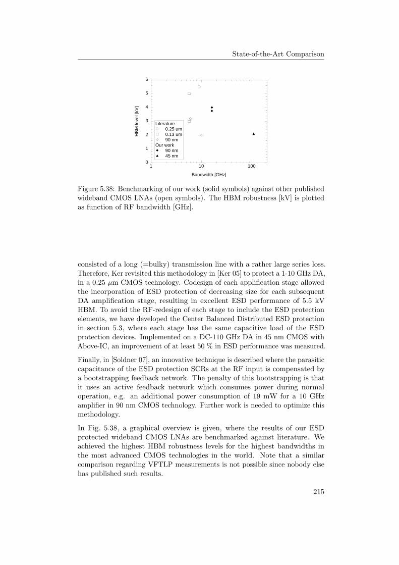
State-of-the-Art Comparison
0
1
2
3
4
5
6
1 10 100
0.25 um0.13 um90 nm
90 nm45 nm
HB
M le
vel [
kV]
Bandwidth [GHz]
Literature
Our work
Figure 5.38: Benchmarking of our work (solid symbols) against other publishedwideband CMOS LNAs (open symbols). The HBM robustness [kV] is plottedas function of RF bandwidth [GHz].
consisted of a long (=bulky) transmission line with a rather large series loss.Therefore, Ker revisited this methodology in [Ker 05] to protect a 1-10 GHz DA,in a 0.25 µm CMOS technology. Codesign of each applification stage allowedthe incorporation of ESD protection of decreasing size for each subsequentDA amplification stage, resulting in excellent ESD performance of 5.5 kVHBM. To avoid the RF-redesign of each stage to include the ESD protectionelements, we have developed the Center Balanced Distributed ESD protectionin section 5.3, where each stage has the same capacitive load of the ESDprotection devices. Implemented on a DC-110 GHz DA in 45 nm CMOS withAbove-IC, an improvement of at least 50 % in ESD performance was measured.
Finally, in [Soldner 07], an innovative technique is described where the parasiticcapacitance of the ESD protection SCRs at the RF input is compensated bya bootstrapping feedback network. The penalty of this bootstrapping is thatit uses an active feedback network which consumes power during normaloperation, e.g. an additional power consumption of 19 mW for a 10 GHzamplifier in 90 nm CMOS technology. Further work is needed to optimize thismethodology.
In Fig. 5.38, a graphical overview is given, where the results of our ESDprotected wideband CMOS LNAs are benchmarked against literature. Weachieved the highest HBM robustness levels for the highest bandwidths inthe most advanced CMOS technologies in the world. Note that a similarcomparison regarding VFTLP measurements is not possible since nobody elsehas published such results.
215
5. ESD Protection for Wideband RF CMOS Circuits
5.5 Conclusions
Providing adequate ESD protection for wideband RF circuits in CMOS is achallenge. Moreover, when these circuits are implemented in the most advancedCMOS technology nodes, larger RF-bandwiths can be obtained which increasesthe ESD design complexity. Simultaneously, the technology itself becomesmore vulnerable to ESD stress.
Very few publications are availabe addressing ESD protection for wideband RFCMOS circuits, specifically for very advanced CMOS technologies. The currentsolutions are either limited in terms of RF performance, power consumption,ESD performance and/or area consumption as was discussed in section 5.4.Therefore, in this chapter two novel ESD protection techniques for widebandRF ESD protection are developed and demonstrated in 90 nm and 45 nmCMOS technologies up to frequencies of 110 GHz.
The T-coil protection from [Galal 03] was transformed into an ESD solutioncompatible with RF requirements, yielding the T-diode concept discussed insection 5.2. Using the T-diode, the parasitic capacitance of the dual-diodeat the RF input is tuned out over a wide frequency band. Input matchingwas maintained from DC to 16.1 GHz, in a 90 nm digital CMOS technology.Two novel ESD techniques were introduced to improve the T-diode ESDprotection. First, local clamping diodes provide a low resistive ESD pathto ground, without relying on current conduction through the power clamp.The additional diode capacitance is compensated by the T-diode. Secondly,addition of turn-off circuitry ensures the turn-on of the power clamp beforetriggering of parasitic current paths in the core circuit. An ESD robustness of4.5 kV HBM and 3.8 A VFTLP was measured.
A novel distributed ESD concept was developed, specifically for distributedamplifier circuits. The developed Center Balanced Distributed ESD protectionimproves current uniformity between the different ESD protection stages. Itcan be easily implemented without the need for redesign of each gain stageand has almost no impact on the RF performance of the circuit. A 1-110 GHzdistributed amplifier in 45 nm CMOS was protected using this methodology,yielding an ESD robustness of 1.4 A TLP and 11.5 A VFTLP.
216
Chapter 6
Conclusions, Future Workand Outlook
ESD is not a showstopper for the introduction of FinFET technology, provideda design methodology to select the delicate layout optimum and adequateprocessing options are applied. Further, efficient ESD solutions can be imple-mented for narrow- and wideband RF circuits which exhibit both excellent RFand ESD performance.
6.1 Conclusions
In this thesis, two major challenges for ESD protection design have beenaddressed. First, the basic ESD performance of common protection devicesimplemented in a SOI FinFET technology has been analyzed. Large depen-dencies on device layout parameters and process options have been found.This has fueled the need for a specific normalization method for accurate datainterpretation and the development of a design methodology to optimize theESD protection structures. Secondly, new ESD protection techniques havebeen developed for both narrow- and wideband RF circuits. These solutionswere shown to have excellent HBM and CDM robustness without significantlydegrading the RF performance. To perform this in depth research, new mea-surement equipment and calibration methods have been developed, whichenabled ESD evaluation of the devices and circuits under more realistic ESDstress conditions.
In Chapter 2, the basic component-level ESD stress models have been discussedtogether with various TLP implementations. These have served as an inputto develop more enhanced ESD characterization and analysis techniques. Byusing a multi-level TLP system, accurate holding voltage determination was
6. Conclusions, Future Work and Outlook
made possible, without being limited by the system loadline. Besides thequasi-static device behavior which is obtained from TLP measurements, alsothe transient device respons could be obtained by analyzing the TLP voltageand current waveforms. These waveforms were calibrated to remove the systemparasitic contributions, revealing the true device behavior. Voltage and currentwaveforms have been captured during HBM stress, yielding an HBM-IV curvefor each HBM stress level. Besides the same quasi-static device informationas obtained from TLP, also HBM transient effects could be studied. A fewexamples of miscorrelation between TLP and HBM have been presented,highlighting the usefulness of HBM-IV.
In Chapter 3, the ESD performance of grounded gate MOS devices and gateddiodes, implemented in a FinFET technology has been studied. Comparedto bulk technologies, an area efficiency of 50 % for NMOS and 30 % forgated diodes was measured. ESD robustness scaling with device width wasdemonstrated, yielding several kV HBM levels for multi-finger multi-fin devices.On the other hand, voltage clamping capability seemed more of a concern dueto the reduced oxide breakdown voltage. The influence of various geometricalparameters on the ESD robustness has been studied. Besides yielding guidelineson how to optimize the device layout for best ESD performance given a setof functional constraints, prediction of the ESD behavior of future FinFETprocessing targets could be established. A performance drop of 50 % waspredicted for the 22 nm FinFET technology node based on further downscalingof the geometrical device parameters. However, the ESD performance wasfound to also heavily depend on the different process options. A large ESDperformance improvement was measured using SEG, which will be standardfor the 22 nm node, and which will restore the ESD performance of the 22 nmnode to a certain extent.
In Chapter 4, the scaling limitations of the classical dual diode protection weredemonstrated. A codesign approach was presented as an alternative solutionwhere the ESD protection was integrated into the RF design. As such, theuse of low-capacitive ESD protection could be extended to higher frequencies,however with limited ESD robustness. When RF frequencies further increase,novel ESD protection strategies are required. We presented an inductive basedESD protection approach, either implemented as a “plug-and-play” inductor toground, or using an RF-ESD codesigned transformer. The impact of inductor-based ESD protection on narrowband RF circuits was studied and their HBMand CDM performance was evaluated. Even though many people question theuse of inductive elements for CDM protection, a high VFTLP robustness levelwas achieved provided high-quality inductors and voltage clamping diodes areused. By codesigning the inductor to ground into a transformer, no additionalarea was required for the ESD inductor. When technology scales further down,higher RF operating frequencies can be achieved. Therefore, the requiredinductance of the ESD protection inductor could be decreased, leading to
218
Future Work
an improved RF performance, ESD performance and area consumption. Assuch, the inductor to ground methodology is preferred over the transformerbased solution because of the reduced design complexity. Very high ESD levelsof 6.3 kV HBM and 7.3 A VFTLP were demonstrated on a 60 GHz LNA,implemented in a 45 nm CMOS technology.
In Chapter 5, two novel wideband RF-ESD protection strategies were presentedto overcome the limitations of the current solutions, in terms of RF performance,power consumption, ESD performance and area consumption. The developedT-coil protection was used to tune out the parasitic ESD diode capacitanceover a wide frequency range, and was demonstrated to work up to 16 GHz. Toimprove the ESD robustness, local clamping at the RF input to the power railswas implemented, and the additional capacitance was compensated by the T-coil network. Turn-off circuitry was added to turn-off any parasitic current paththrough the core circuit during the ESD stress. These improvements resultedin an ESD robustness of 4.5 kV HBM and 3.8 A VFTLP on a 90 nm CMOSLNA. Further, a novel distributed ESD concept was developed, improving thecurrent uniformity between the different ESD protection stages. An increasewith 50 % TLP and 32 % VFTLP over the conventional solution was obtainedon a 1-110 GHz DA in 45 nm CMOS.
6.2 Future Work
At the end of this PhD, I would like to make some recommendations for futureresearch in this field.
1. As many manufacturers of integrated circuits face the difficulty of provi-ding reliable products to system vendors even without knowing the finalapplication, a clear need is present to correlate system-level ESD behaviorwith component-level ESD characterization results. The first steps havebeen taken in section 2.3.2, where on-wafer measurements of system-levelstress using the Human Metal Model (HMM) were performed. Firstresults indicated a large dependence of the correlation factor betweenHBM and HMM, depending on the device type being considered. Moreunderstanding is needed regarding the underlying physical reasons forsuch differences. Future work will need to address the relationship be-tween ESD robustness on wafer-level, package-level and complete systemlevel.
2. The ESD performance evaluation performed in this thesis on SOI FinFETdevices needs to be further expanded. Some items are still open regardingthe impact on area efficiency by folding of the multi-finger transistors,and regarding the different failure mechanisms in multi-fin groundedgate NMOS transistors. For the latter, failure analysis should provide
219
6. Conclusions, Future Work and Outlook
clear answers. Future work to study the turn-on and failure uniformityof FinFET devices is planned using Transient Interferometric Mapping(TIM) [Furb 00]. The TIM technique is a powerful tool to analyze internaltemperature and free carrier distribution in ESD protection devices, butit is a question whether high enough spatial resolution for FinFET devicescan be reached.
3. In this thesis, FinFET devices are fabricated on SOI substrate. However,SOI wafers have disadvantages with respect to their self-heating proper-ties, cost, defect density etc., when compared to bulk silicon substrates.In addition, bulk silicon substrates are compatible with the existingstandard planar CMOS process technologies [Okan 05]. It is thereforeuseful and cost-effective to implement FinFET technology on bulk siliconwafers. A TEM cross-section of a multi-fin bulk FinFET is shown inFig. 6.1. Only the top part of the fin above the SiO2, indicated by Hfin,is surrounded by the gate. The fin is connected by a triangular shape tothe silicon substrate, which makes the fin height definition difficult. Firstcharacterization results have been performed on bulk FinFET structuresand are compared to SOI FinFET results. Fig. 6.2 shows the IV curvesfor both bulk and SOI narrow-fin NMOS FinFETs with different gatelength stressed in parasitic bipolar mode. For SOI FinFETs no snapbackis observed as the parasitic BJT has its base floating. For bulk FinFETsno snapback is observed for short gate lengths (≤ 70 nm) either, whilefor medium and long gate lengths the IV curves are similar to the onesof planar MOS technologies, where the holding voltage is distinct fromthe triggering voltage. A different Lg dependency of It2 is observed. ForSOI FinFET, It2 increases with increasing Lg, as the current uniformityat high current levels increases with increasing Lg, and slightly dropsdown for the largest Lg, as the dissipated energy is increased due tothe increase in voltage drop (Vh). This leads to a maximum intrinsicIt2 (11.5 mA/µm) at medium Lg. On the contrary, for bulk FinFETsIt2 decreases monotonically with increasing Lg, leading to a maximumintrinsic It2 (41.1 mA/µm) at the smallest Lg. This higher robustnesscan mainly be attributed to the trapezoidal fin shape of bulk FinFETs(Fig. 6.1), which improves the heat dissipation through the bulk siliconand to the increased junction area because of the addition of the bottomjunction. Moreover, for medium and long Lg, It2 is unexpected lowerthan for SOI FinFETs. Gate-oxide breakdown could be the reason forthis early failure. An improvement up to 3.5x in maximum It2 is observedfor narrow-fin bulk FinFETs over SOI FinFETs. More details on theseinitial results on the ESD performance of bulk FinFET devices can befound in [Griff 09].
4. Throughout this thesis, several narrow- and wideband RF-ESD protectionmethodologies have been developed and analyzed regarding their ESDand RF performance. A lot of further research still can be done in this
220
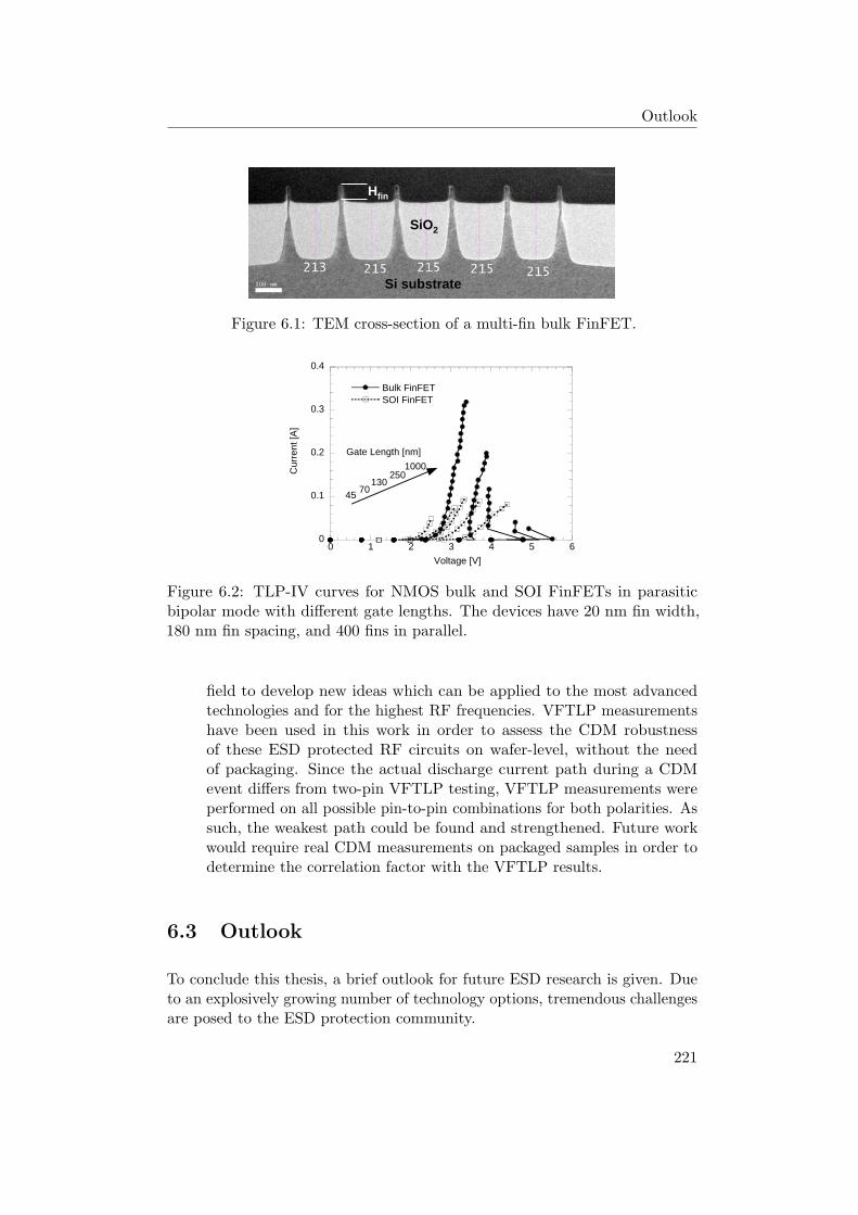
Outlook
SiO2
Hfin
Si substrate
Figure 6.1: TEM cross-section of a multi-fin bulk FinFET.
0
0.1
0.2
0.3
0.4
0 1 2 3 4 5 6
Bulk FinFETSOI FinFET
Voltage [V]
Cur
rent
[A]
4570
130250
1000
Gate Length [nm]
Figure 6.2: TLP-IV curves for NMOS bulk and SOI FinFETs in parasiticbipolar mode with different gate lengths. The devices have 20 nm fin width,180 nm fin spacing, and 400 fins in parallel.
field to develop new ideas which can be applied to the most advancedtechnologies and for the highest RF frequencies. VFTLP measurementshave been used in this work in order to assess the CDM robustnessof these ESD protected RF circuits on wafer-level, without the needof packaging. Since the actual discharge current path during a CDMevent differs from two-pin VFTLP testing, VFTLP measurements wereperformed on all possible pin-to-pin combinations for both polarities. Assuch, the weakest path could be found and strengthened. Future workwould require real CDM measurements on packaged samples in order todetermine the correlation factor with the VFTLP results.
6.3 Outlook
To conclude this thesis, a brief outlook for future ESD research is given. Dueto an explosively growing number of technology options, tremendous challengesare posed to the ESD protection community.
221
6. Conclusions, Future Work and Outlook
Besides novel device architectures such as 3D-FinFET devices, also new mate-rials may be used to continue down Moore’s road. New high mobility channelssuch as germanium and III-V compounds may be needed for future devicegenerations.
In general, ESD protection for high voltage technologies still holds a lot ofchallenges.
Further, the study of the reliability and failure mechanisms of Micro Electro-Mechanical System (MEMS) actuators under ESD stress has received increasingattention in recent times. Very high sensitivity levels towards ESD have beendemonstrated already for micromirrors. RF-MEMS ohmic and capacitiveswitches have also been shown to have serious reliability problems both underDC and ESD stress.
Carbon Nano Tubes (CNT) and graphene nanoribbons are currently beingresearched since they have many properties, from their unique dimensions (adiameter close to 1 nm, while their length can be up to 1000 times longer) toan unusual current conduction mechanism, that make them ideal componentsfor electrical circuits. No ESD results have been published so far.
IMEC recently demonstrated the first functional 3D integrated circuits ob-tained by die-to-die stacking using 5 µm Cu Through-Silicon Vias (TSV). 3Dintegration seems promising for system integration with applications rangingfrom electronics for consumer, automotive and medical applications. Duringthe stacking process, CDM-like discharge events could occur from die to dieand therefore adequate ESD protection would be required. Due to increased in-terconnect resistances across the different dies, novel ESD protection strategiesmight be required.
Other exciting new technology developments include biosensors, neurons-on-chip, plastic and organic electronics, etc. Little or nothing is known how thesetechnologies behave under ESD stress conditions. Therefore, there are manyunexplored ESD problems which are waiting for new solutions.
ESD will remain a challenge for the next years to come!
222
Bibliography
[Amer 02] A. Amerasekara and C. Duvvury, ESD in Silicon IntegratedCircuits, 2nd ed. J. Wiley & Sons, 2002.
[ASITIC] Asitic. [Online]. Available: http://rfic.eecs.berkeley.edu/∼niknejad/asitic.html
[Auge 05] E. Augendre, G. Eneman, A. D. Keersgieter, V. Simons,I. D. Wolf, J. Ramos, S. Brus, B. Pawlak, S. Severi, F. Leys,E. Sleeckx, S. Locorotondo, M. Ercken, J. de Marneffe,L. Fei, M. Seacrist, B. Kellerman, M. Goodwin, K. D.Meyer, M. Jurczak, and S. Biesemans, “On the Scalabilityof Source/Drain Current Enhancement in Thin Film sSOI,”in European Solid-State Device Research Conference, 2005,pp. 301–304.
[Bagh 06] R. Bagheri, A. Mirzaei, S. Chehrazi, M. Heidari, M. Lee,M. Mikhemar, T. WAI, and A. Abidi, “An 800 MHz 6 GHzSoftware-Defined Wireless Receiver in 90 nm CMOS,” IEEEJournal of Solid-State Circuits, vol. 41, 12, pp. 2860–2876,Dec. 2006.
[Bata 94] C. Batard, D. Smith, H. Zelaya, and C. Goodman, “Newhigh power diode model with both forward and reverserecovery,” IEEE Power electronics & Variable Speed driver,pp. 447–452, 1994.
[Bhat 06] K. Bhatia, S. Hyvonen, and E. Rosenbaum, “An 8 mW, ESD-protected, CMOS LNA for Ultra-Wideband Applications,”in IEEE Custom Integrated Circuits Conference, 2006, pp.385–388.
[Borr 07] J. Borremans, S. Thijs, P. Wambacq, D. Linten, Y. Rolain,and M. Kuijk, “A 5 kV HBM Transformer-Based ESDProtected 5-6 GHz LNA,” 2007, pp. 100–101.
[Borr 08] J. Borremans, B. Parvais, M. Dehan, S. Thijs, P. Wambacq,A. Mercha, M. Kuijk, G. Carchon, and S. Decoutere, “Per-spective of RF design in future planar and FinFET CMOS,”in IEEE Radio Frequency IC Symposium, 2008, pp. 75–78.
[Borr 09] J. Borremans, K. Raczkowski, and P. Wambacq, “ADigitally-Controlled Compact 57-66 GHz Receiver Front-End for Phased-Arrays in 45 nm Digital CMOS,” in IEEEInternational Solid-State Circuits Conference, 2009, p. tobe completed.
[Borremans 07b] J. Borremans, P. Wambacq, and D. Linten, “An ESD-Protected DC-to-6 GHz 9.7 mW LNA in 90 nm Digital
223
Bibliography
CMOS,” in IEEE International Solid-State Circuits Confe-rence, 2007, pp. 422–423.
[Bose 05] G. Boselli and C. Duvvury, “Analysis of ESD ProtectionComponents in 65 nm CMOS Technology: Scaling Perspec-tive and Impact on ESD Design Window,” in EOS/ESDSymposium Proceedings, 2005, pp. 43–52.
[Bren 05] C. Brennan, C. Shunhua, M. Woo, K. Chatty, and R. Gau-thier, “Implementation of Diode and Bipolar TriggeredSCRs for CDM robust ESD protection in 90nm ASICS,”in EOS/ESD Symposium Proceedings, 2005, pp. 380–386.
[Carch 04] G. Carchon, W. D. Raedt, and E. Beyne, “Wafer-level pa-ckaging technology for High-Q On-chip Inductors and Trans-mission Lines,” IEEE Transactions on Microwave Theoryand Techniques, vol. 52, 4, 2004.
[Carch 05] G. Carchon, X. Sun, G. Posada, D. Linten, and E. Beyne,“Thin-film as enabling passive integration technology for RFSoC and SiP,” in IEEE International Solid-State CircuitsConference, 2005, pp. 398–399.
[CDM 08] Field-Induced Charged-Device Model Test Method forElectrostatic-Discharge-Withstand Thresholds of Microelec-tronic Components, Jesd22-c101d ed. JEDEC Standard,October 2008.
[CDM 99] ESD Sensitivity testing, Charged Device Model (CDM)-Component Level, chapter S5.3. ESD Association Standard,1999.
[Chen 07] T. W. Chen, C. Ito, T. Maloney, W. Loh and R. Dut-ton, “Gate Oxide Reliability Characterization in the 100 psRegime with Ultra-fast Transmission Line Pulsing System,”in EOS/ESD Symposium Proceedings, 2007, pp. 102–106.
[Choi 04] J. A. Choi, K. Lee, Y. Jin, Y. Lee, S. Lee, G. Leet, S. Lee,M. Sun, D. Kimt, Y. Lee, S. Bae, J. Yang, S. Maeda, N. Lee,H. Kang, and K. Suh, “Large Scale Integration and Relia-bility Consideration of Triple Gate Transistors,” in IEEEInternational Electron Devices Meeting, 2004, pp. 647–650.
[Clif 93] M. L. Cliff and P. Lauritzen, “A simple power diode modelwith forward and reverse recovery,” IEEE Trans. PowerElectron, vol. 8,4, pp. 342–346, 1993.
[Coll 05] N. Collaert, M. Demand, I. Ferain, J. Lisoni, R. Singana-malla, P. Zimmerman, Y. Yim, T. Schram, G. Mannaert,M. Goodwin, J. Hooker, F. Neuilly, M. Kim, K. D. Meyer,S. D. Gendt, W. Boullart, M. Jurczak, and S. Biesemans,
224
“Tall Triple-Gate Devices with TiN/HfO2 Gate Stack,” inIEEE Symposium on VLSI Technology, 2005, pp. 108–109.
[Coll 05b] N. Collaert, A. D. Keersgieter, K. Anil, R. Rooya-ckers, G. Eneman, M. Goodwin, B. Eyckens, E. Sleeckx,J. de Marneffe, K. D. Meyer, P. Absil, M. Jurczak, andS. Biesemans, “Performance Improvement of Tall TripleGate Devices with strained SiN layers,” IEEE Electron Dev.Lett, vol. 26,11, pp. 820–822, Nov. 2005.
[Coll 07] N. Collaert, A. D. Keersgieter, A. Dixit, I. Ferain, L. Lai,D. Lenoble, A. Mercha, A. Nackaerts, B. Pawlak, R. Rooya-ckers, T. Schulz, K. San, N. Son, M. V. Dal, P. Verheyen,K. von Arnim, L. Witters, K. D. Meyer, S. Biesemans, andM. Jurczak, “Multi-Gate Devices for the 32 nm TechnologyNode and Beyond,” in European Solid-State Device ResearchConference, 2007, pp. 143–146.
[Coll 07c] N. Collaert, R. Rooyackers, G. Dilliway, V. Iyengar, E. Au-gendre, F. Leys, I. Cayrefourq, B. Ghyselen, R. Loo, M. Jur-czak, and S. Biesemans, “Optimization of the MuGFETperformance on Super Critical-Strained SOI (SC-SSOI) sub-strates featuring raised source/drain and dual CESL,” inVLSI Technology, Systems and Applications, 2007, pp. 1–2.
[Coll 08] N. Collaert, R. Rooyackers, A. Hikavy, A. Dixit, F. Leys,P. Verheyen, R. Loo, M. Jurczak, and S. Biesemans, “Multi-gate devices for the 32nm Technology Node and Beyond:Challenges for Selective Epitaxial Growth,” Thin SolidFilms, vol. 517,1, pp. 101–104, Nov. 2008.
[Daen 04] T. Daenen, S. Thijs, M. Natarajan, V. D. Heyn, V. Vas-silev, and G. Groeseneken, “Multilevel Transmission LinePulse (MTLP) Tester,” in EOS/ESD Symposium Procee-dings, 2004, pp. 316–321.
[Deib 89] S. Deibele and J. Beyer, “Attenuation Compensation inDistributed Amplifier Design,” IEEE Transactions on Mi-crowave Theory and Techniques, vol. 37, 9, pp. 1425 – 1433,Sep. 1989.
[Dixi 05] A. Dixit, K. Anil, N. Collaert, M. Goodwin, M. Jurczak,and K. D. Meyer, “Analysis of the Parasitic Source/DrainResistance in Multiple gate Field Effect Transistors,” IEEETrans. Electron Dev., vol. 52,6, pp. 1132–1140, 2005.
[Dixi 06] A. Dixit, K. Anil, N. Collaert, P. Zimmerman, M. Jurczak,and K. D. Meyer, “Minimization of MuGFET Source/Drain
225
Bibliography
Resistance using Wrap-Around NiSi Contacts,” IEEE Jour-nal of Solid-state Electronics, vol. 50,7-8, pp. 1466–1471,2006.
[Duvv 07] C. Duvvury, “Keynote Speach - Activities of Industry Coun-cil on ESD Targets,” in EOS/ESD Symposium Proceedings,2007.
[Duvv 08] C. Duvvury, “Paradigm Shift in ESD Qualification,” 2008,pp. 1–2.
[Duvv 92] C. Duvvury and C. Diaz, “Dynamic Gate Coupled NMOSfor Efficient Output ESD Protection,” 1992, pp. 141–150.
[ESDA] Electrostatic discharge association standards, standardtest methods, standard practices. [Online]. Available:http://www.esda.org/standardlistings.html
[Feuc 90] D. Feucht, Handbook of Analog Circuit Design, academic ed.,San Diego, CA, 1990.
[Fuji 05] M. Fujiwara, T. Morooka, N. Yasutake, K. Ohuchi, N. Aoki,H. Tanimoto, M. Kondo, K. Miyano, S. Inaba, K. Ishimaru,and H. Ishiuchi, “Impact of BOX Scaling on 30 nm GateLength FD SOI MOSFET,” in IEEE International SOIConference, 2005, pp. 180–182.
[Furb 00] C. Furb, K. Esmark, M. Litzenberger, D. Pogany, G. Groos,R. Zelsacher, M. Stecher, and E. Gornik, “Thermal andFree Carrier Concentration Mapping during ESD event inSmart Power ESD Protection Devices using an ImprovedLaser Interferometric Technique,” Journal of Microelectro-nics Reliability, vol. 40, pp. 1365–1370, 2000.
[Galal 03] R. Galal and B. Razavi, “Broadband ESD Protection Cir-cuits in CMOS Technology,” IEEE Journal of Solid-StateCircuits, vol. 38, pp. 2334–2340, Dec. 2003.
[Gies 98] H. Gieser and M. Haunschild, “Very Fast Transmission LinePulsing of Integrated Structures and the Charge DeviceModel,” IEEE Transaction on Components, Packaging, andManufacturing Technology, vol. 21-C, Oct. 1998.
[Goss 06] H. Gossner, C. Russ, F. Siegelin, J. Schneider, K. Schruefer,T. Schulz, C. Duvvury, C. Cleavelin, and W. Xiong, “UniqueESD Failure Mechanism in a MuGFET Technology,” inIEEE International Electron Devices Meeting, 2006, pp.101–104.
[Griff 09] A. Griffoni, S. Thijs, C. Russ, D. Tremouilles, D. Linten,M. Scholz, N. Collaert, L. Witters, G. Meneghesso, and
226
G. Groeseneken, “Next Generation FinFET Devices in BulkSilicon Technology and Their Benefits for ESD Robustness,”in EOS/ESD Symposium Proceedings, 2009, p. To be pu-blished.
[HBM 07] For Electrostatic Discharge Sensitivity Testing Human BodyModel (HBM) Component Level. ESD Association Standard,2007.
[HBM 07b] Electrostatic Discharge Sensitivity Testing Human BodyModel, Jesd22-a114-e ed. JEDEC Standard, 2007.
[HFSS] Hfss. [Online]. Available: www.ansoft.com/products/hf/hfss
[Hoff 05] T. Hoffmann, G. Doornbos, I. Ferain, N. Collaert, P. Zim-merman, M. Goodwin, R. Rooyackers, A. Kottantharayil,K. Anil, Y. Yim, M. Jurczak, and S. Biesemans, “GIDLand Parasitic Schottky Barrier Leakage Elimination inAggressively Scaled HfO2/TiN FinFET Devices,” in IEEEInternational Electron Devices Meeting, 2005, pp. 725–728.
[Horng 03] T. Horng, J. Wu, L. Yang, and S. Fang, “A novel Modified-TEquivalent Circuit for Modeling LTCC Embedded Inductorswith a Large Bandwidth,” IEEE Tranactions on MicrowaveTheory and Techniques, vol. 51, 12, pp. 1015–1018, Dec.2003.
[Howa 65] N. Howard and G. Johnson, “P+-i-n+ Silicon Diodes atHigh Forward Current Densities,” Solid State Electronics,vol. 8, pp. 275–284, 1965.
[Huang 09] B. Huang, C. Wang, C. Chen, M. Lei, P. Huang, K. Lin, andH. Wang, “Design and Analysis for a 60-GHz Low-NoiseAmplifier With RF ESD Protection,” IEEE Transactions onMicrowave Theory and Techniques, vol. 57, 2, pp. 298–305,2009.
[Hyat 00] H. Hyatt, J. Harris, A. Alanzo, and P. Bellew, “TLP Mea-surements for Verification of ESD Protection Device Re-sponse,” in EOS/ESD Symposium Proceedings, 2000, pp.111–121.
[Hyvo 03] S. Hyvonen, S. Joshi, and E. Rosenbaum, “ComprehensiveESD protection for RF inputs,” in EOS/ESD SymposiumProceedings, 2003, pp. 188–19.
[Hyvo 03b] S. Hyvonen, S. Joshi, and E. Rosenbaum, “Cancellationtechnique to provide ESD protection for multi-GHz RFinputs,” Electronic Letters, vol. 39, 3, pp. 284–286, 2002.
227
Bibliography
[IEC 01] Electromagnetic Compatibility (EMC) Part 4-2: Testingand Measurement Techniques Electrostatic Discharge Immu-nity Test, Iec 61000-4-2 ed. International ElectrotechnicalCommission (IEC), 2007.
[Ille 06] A. Ille, W. Stadler, A. Kerber, T. Pompl, T. Brodbeck,K. Esmark, and A. Bravaix, “Ultra-thin Gate Oxide Relia-bility in the ESD Time Domain,” in EOS/ESD SymposiumProceedings, 2006, pp. 285–294.
[InCo 07] Industry council on esd target levels. [Online]. Available:http://www.esdtargets.blogspot.com/
[Issa 08] V. Issakov, D. Johnsson, Y. Cao, M. Tiebout, M. Mayerhofer,W. Simburger, and L. Maurer, “ESD Concept for High-Frequency Circuits,” in EOS/ESD Symposium Proceedings,2008, pp. 221–227.
[ITRS] International technology roadmap for semiconductors.[Online]. Available: http://www.itrs.net
[JEDE 08] Recommended esd target levels for hbm/mm qualification.[Online]. Available: http://www.jedec.org/DOWNLOAD/search/JEP155.pdf
[Junj 07] J. Li, R. Gauthier, K. Chatty, S. Mitra, H. Li, X. Wang,R. Halbach, and C. Seguin, “Capacitance Investigation ofDiodes and SCRs for ESD Protection of High FrequencyCircuits in Sub-100 nm Bulk CMOS Technologies,” inEOS/ESD Symposium Proceedings, 2007, pp. 250–256.
[Junj 08] J. Li, S. Mitra, H. Li, M. Abou-Khalil, K. Chatty, andR. Gauthier, “Capacitance Investigation of Diode and GGN-MOS for ESD Protection of High Frequency Circuits in45 nm SOI CMOS Technologies,” in EOS/ESD SymposiumProceedings, 2008, pp. 228–234.
[Kedz 03] J. Kedzierski, M. Ieong, E. Nowak, T. Kanarsky, Y. Zhang,R. Roy, D. Boyd, D. Fried, and H. P. Wong, “Extensionand Source/Drain Design for High Performance FinFETDevices,” IEEE Trans. Electron Dev., vol. 50,4, pp. 952–958,2003.
[Kepp 06] B. Keppens, G. Wybo, G. Vermont, and B. V. Camp, “Con-cept for Body Coupling in SOI MOS Transistor to ImproveMulti-Finger Triggering,” in EOS/ESD Symposium Procee-dings, 2006, pp. 172–178.
[Ker 03] M. D. Ker and C. Lee, “ESD Protection Design for Giga-HzRF CMOS LNA with Novel Impedance-Isolation Technique,”in EOS/ESD Symposium Proceedings, 2003, pp. 204–213.
228
[Ker 05] M. D. Ker, Y. Hsiao, and B. Kuo, “ESD Protection Designfor 1 to 10 GHz Distributed Amplifier in CMOS Technology,”IEEE Transactions on Microwave Theory and Techniques,vol. 53, 9, pp. 2672–2681, Sep. 2005.
[Ker 99] M. D. Ker and S. Liu, “Whole-Chip ESD Protection De-sign with Efficient VDD-to-VSS ESD Clamp Circuits forSubmicron CMOS VLSI,” IEEE Transactions on ElectronDevices, vol. 46, 1, pp. 173–183, Jan. 1999.
[Kimura 96] S. Kimura, Y. Imai, Y. Umeda, and T. Enoki, “Loss-compensated Distributed Baseband Amplifier IC’s for Op-tical Transmission Systems,” IEEE Transactions on Mi-crowave Theory and Techniques, vol. 44, 10, pp. 1688 –1693, Oct. 1996.
[Klev 00] B. Kleveland, T. Maloney, I. Morgan, L. Madden, T. Lee,and S. Wong, “Distributed ESD Protection for High-SpeedIntegrated Circuits,” IEEE Electron Device Letters, vol. 21,pp. 390–392, Aug. 2000.
[LaPe 07] M. LaPedus, “ESD Plan: State of Shock,” EE Times, 072007.
[Lee 01] J. Lee, Y. Huh, P. Bendix, and S. Kang, “Design-for-ESD-reliability for high-frequency I/O interfacecircuits in deep-submicron CMOS technology,” in IEEE International Sym-posium on Circuits and Systems, 2001, pp. 746–749.
[Lee 98] T. H. Lee, The design of CMOS Radio-Frequency IntegratedCircuits. Cambridge University Press, 1998.
[Lero 04] P. Leroux and M. Steyaert, “A 5 GHz CMOS Low-NoiseAmplifier with Inductive ESD Protection Exceeding 3 kVHBM,” in Proc European Solid-State Circuits Conference,2004, pp. 295–298.
[Li 06] J. Li, S. Joshi, R. Barnes, and E. Rosenbaum, “CompactModeling of On-chip ESD Protection Devices Using Verilog-A,” IEEE J. Computer-aided design of Integrated Circuitsand Systems, vol. 25,6, pp. 1047–1063, 2006.
[Lint 05] D. Linten, S. Thijs, M. Natarajan, P. Wambacq, W. Jeam-saksiri, J. Ramos, A. Mercha, S. D. S. Jenei, and S. Decou-tere, “A 5 GHz Fully Integrated ESD-Protected Low-NoiseAmplifier in 90 nm RF CMOS,” IEEE Journal of Solid-StateCircuits, vol. 40, 7, pp. 1434–1442, 2005.
[Lint 08] D. Linten, V. Vashchenko, M. Scholz, P. Jansen, D. La-fonteese, S. Thijs, M. Sawada, T. Hasebe, P. Hopper, andG. Groeseneken, “Extreme Voltage and Current Overshoots
229
Bibliography
in HV Snapback Devices during HBM ESD stress,” inEOS/ESD Symposium Proceedings, 2008, pp. 204–210.
[Malo 85] T. Maloney and N. Khurana, “Transmission Line PulseTechnique for Circuit Modeling and ESD Phenomena,” inEOS/ESD Symposium Proceedings, 1985, pp. 49–54.
[McDa 89] L. McDaid, S. Hall, P. Mellor, and W. Eccleston, “PhysicalOrigin of Negative Differential Resistance in SOI Transis-tors,” Electronics Letters, vol. 25, 13, pp. 827–828, 1989.
[Merg 03] M. Mergens, C. Russ, K. Verhaege, J. Armer, P. Jozwiak,R. Mohn, B. Keppens, and C. Trinh, “Diode-triggered SCR(DTSCR) for RF-ESD protection of BiCMOS SiGe HBTsand CMOS ultra-thin gate oxides,” in IEEE InternationalElectron Devices Meeting, 2003, pp. 21.3.1–21.3.4.
[Merg 04] M. Mergens, J. Armer, P. Jozwiak, B. Keppens, F. D. Ranter,K. Verhaege, and R. Kumar, “Active-Source-Pump (ASP)Technique for ESD Design Window Expansion and Ultra-Thin Gate Oxide Protection in Sub-90nm Technologies,”in IEEE Custom Integrated Circuits Conference, 2004, pp.251–254.
[Mil 96] Military Standard MIL-STD 883E. MIL, 1996.
[Mill 57] S. L. Miller, “Ionization Rates for Holes and Electrons inSilicon,” Phys. Rev., vol. 105, p. 12461249, 1957.
[MM 97] Electrostatic Discharge Sensitivity Testing Machine Model,Jesd22-a115-a ed. JEDEC Standard, 1997.
[MM 99] For Electrostatic Discharge Sensitivity Testing MachineModel (MM) Component Level. ESD Association Standard,1999.
[OCon 03] R. O’Connor, R. Degraeve, B. Kaczer, A. Veloso, G. Hughes,and G. Groeseneken, “Weibull Slope and Voltage Accele-ration of Ultra-thin (1.1-1.45 nm EOT) Oxynitrides,” inProceedings INFOS, 2003, p. GS26.
[Okan 05] K. Okano, T. Izumida, H. Kawasaki, A. Kaneko, A. Yagi-shita, T. Kanemura, M. Kondo, S. Ito, N. Aoki, K. Miyano,T. Ono, K. Yahashi, K. Iwade, T. Kubota, T. Matsushita,I. Mizushima, S. Inaba, K. Ishimaru, K. Suguro, K. Eguchi,Y. Tsunashima, and H. Ishiuchi, “Process Integration Tech-nology and Device Characteristics of Bulk CMOS FinFETs,”in IEEE International Electron Devices Meeting, 2005, pp.721–724.
230
[Parv 07] B. Parvais, M. Dehan, V. Subramanian, A. Mercha, K. T.San, M. Jurczak, G. Groeseneken, W. Sansen, and S. De-coutere, “Analysis of the FinFET Parasitics for ImprovedRF Performances,” in IEEE International SOI Conference,2007, pp. 37–3.
[Pava 05] C. Pavageau, M. Moussa, A. Siligaris, L. Picheta, F. Dan-neville, J. Raskin, D. Vanhoenaker-Janvier, J. Russat, andN. Fel, “Low power 23-Ghz and 27-Ghz distributed cascodeamplifiers in a standard 130nm SOI CMOS process,” IEEETranactions on Microwave Theory and Techniques, vol. 12,17, pp. 2243 – 2246, 2005.
[Peach 08] N. Peachey, “ESD Open Forum - ESD Stressing of Devicesand Components,” Conformity Magazine, vol. 13,6, pp. 22–23, 2008.
[PhDBorremans] J. Borremans, “Area-Aware RF Front-End Circuit Designin Nanometer CMOS,” Ph.D. dissertation, Vrije UniversiteitBrussel (VUB), Brussels, Belgium, Aug. 2008.
[PhDLinten] D. Linten, “Evaluation of Deep-sub-quarter Micron CMOSTechnology: Low Noise Amplifiers, Oscillators and ESDReliability,” Ph.D. dissertation, Vrije Universiteit Brussel(VUB), Brussels, Belgium, Jan. 2006.
[PhDPavageau] C. Pavageau, “Utilisation des Technologies CMOS SOI130 nm pour des Applications en Gamme de FrequenceMillimetrique,” Ph.D. dissertation, University of Lille, Vil-leneuve d’Ascq, France, Dec. 2005.
[PhDSubramanian] V. Subramanian, “Study of Analog and RF Performanceof Multiple Gate Field Effect Transistors for Future CMOSTechnologies,” Ph.D. dissertation, Katholieke UniversiteitLeuven (KUL), Leuven, Belgium, May 2008.
[PhDTremouilles] D. Tremouilles, “Optimisation et modelisation de protec-tions integrees contre les decharges electrostatiques, parl’analyse de la physique mise en jeu,” Ph.D. dissertation, In-stitut National des Sciences Appliquees de Toulouse, France,2004.
[Putn 04] C. Putnam, M. Woo, R. Gauthier, M. Muhammad,K. Chatty, C. Seguin, and R. Halbach, “An Investigationhof ESD Protection Diode Options in SOI,” in Proc. IEEEInternational SOI Conference, 2004, pp. 24–26.
[Racz 09] K. Raczkowski, S. Thijs, W. D. Raedt, B. Nauwelaers, andP. Wambacq, “50-67 GHz ESD Protected Power Amplifiersin Digital 45 nm LP CMOS,” in IEEE International Solid-State Circuits Conference, 2009, p. 22.5.
231
Bibliography
[Rich 00] C. Richier, P. Salome, G. Mabboux, I. Zaza, A. Juge,and P. Mortini, “Investigation on Different ESD Protec-tion Strategies Devoted to 3.3 V RF Applications (2 Ghz)in a 0.18 µm CMOS Process,” in EOS/ESD SymposiumProceedings, 2000, pp. 251–259.
[Rooy 06] R. Rooyackers, E. Augendre, B. Degroote, N. Collaert,A. Nackaerts, A. Dixit, T. Vandeweyer, B. Pawlak, M. Er-cken, E. Kunnen, G. Dilliway, F. Leys, R. Loo, M. Jurczak,and S. Biesemans, “Doubling or Quadrupling MuGFET FinIntegration Scheme with Higher Pattern Fidelity, Lower CDVariation and Higher Layout Efficiency,” in IEEE Interna-tional Electron Devices Meeting, 2006, pp. 1–4.
[Russ 05] C. Russ, H. Gossner, T. Schulz, N. Chaudhary, W. Xiong,A. Marshall, C. Duvvury, K. Schrfer, and C. Cleavelin,“ESD Evaluation of the Emerging MuGFET Technology,” inEOS/ESD Symposium Proceedings, 2005, pp. 280–289.
[Russ 07] C. Russ, H. Gossner, T. Schulz, N. Chaudhary, W. Xiong,A. Marshall, C. Duvvury, K. Schrfer, and C. Cleavelin, “ESDEvaluation of the Emerging MuGFET Technology,” IEEETransaction on Device and Materials Reliability, vol. 7, pp.152–161, Mar. 2007.
[Russ 08] C. Russ, “ESD Issues in Advanced CMOS Bulk and FinFETTechnologies: Processing, Protection Devices and CircuitStrategies,” Journal of Microelectronics Reliability, vol. 48,p. 14031411, 2008.
[Salm 04] A. Salman, M. Pelella, S. Beebe, and N. Subba, “ESDProtection for SOI Technology using an Under-The-Box(Substrate) Diode Structure,” in EOS/ESD Symposium Pro-ceedings, 2004, pp. 248–254.
[Sche 08] K. Scheir, S. Bronckers, J. Borremans, P. Wambacq, andY. Rolain, “A 52 GHz Phased-Array Receiver Front-End in90 nm Digital CMOS,” in IEEE International Solid-StateCircuits Conference, 2008, pp. 184–605.
[Scho 07] M. Scholz, D. Tremouilles, D. Linten, Y. Rolain, R. Pintelon,M. Sawada, T. Nakaei, T. Hasebe, and G. Groeseneken,“Faster ESD device characterization with wafer-level HBM,”in Proceedings IEEE ICMTS, 2007, pp. 93–96.
[Scho 07b] M. Scholz, S. Thijs, D. Linten, D. Tremouilles, M. Sawada,T. Nakaei, T. Hasebe, M. Natarajan, and G. Groeseneken,“Calibrated Wafer-Level HBM Measurements for Quasi-Static & Transient Device Analysis,” in EOS/ESD Sympo-sium Proceedings, 2007, pp. 89–94.
232
[Scho 08] M. Scholz, D. Linten, S. Thijs, S. Sangameswaran,M. Sawada, T. Nakaei, T. Hasebe, and G. Groeseneken,“ESD on-wafer characterization: Is TLP still the right mea-surement tool?” IEEE Transactions on Instrumentationand Measurement, vol. IM-08-971R, to be published 2008.
[Scho 08b] M. Scholz, D. Linten, S. Thijs, M. Sawada, T. Nakaei,T. Hasebe, and G. Groeseneken, “On-wafer Human MetalModel System-level ESD Stress on Component Level.”
[Schu 08] D. Schutz, “10 Common Myths About Static Electricity,”Conformity, Jan. 2008. [Online]. Available: www.conformity.com
[Shae 97] D. K. Shaeffer and T. Lee, “A 1.5V 1.5 GHz CMOS LowNoise Amplifier,” IEEE Journal of Solid-State Circuits,vol. 32, pp. 745–759, May 1997.
[Shen 91] K. Shenai, “Electron mobilities in MOS channels formedalong anisotropically dry etched (110) silicon trench side-walls,” IEEE Electron. Lett., vol. 27,9, pp. 715–717, Jan.1991.
[Shin 05] K. Shin, C. Chui, and T. King, “Dual Stress Capping LayerEnhancement Study for Hybrid Orientation FinFET CMOSTechnology,” in IEEE International Electron Devices Mee-ting, 2005, pp. 1009–101.
[Sold 05] W. Soldner, M. Streibl, U. Hodel, M. Tiebout, H. Gossner,D. S. Landsiedel, J. Chun, C. Ito, and R. Dutton, “RF ESDProtection Strategies: Codesign vs. low-C Protection,” inEOS/ESD Symposium Proceedings, 2005, pp. 33–42.
[Soldner 07] W. Soldner, M. Kim, M. Streibl, H. Gossner, T. Lee, andD. Schmitt-Landsiedel, “A 10 GHz Broadband Amplifierwith Bootstrapped 2 kV ESD Protection,” in IEEE Interna-tional Solid-State Circuits Conference, 2007, pp. 550–551.
[Stad 04] W. Stadler, S. Bargstadt-Franke, T. Brodbeck, R. Gaertner,M. Goroll, H. Gossner, N. Jensen, and C. Muller, “Fromthe ESD Robustness of Products to the System ESD Ro-bustness,” in EOS/ESD Symposium Proceedings, 2004, p.6774.
[Stoc 06] M. Stockinger and J. Miller, “Characterization and Modelingof Three CMOS Diode Structures in the CDM to HBMTimeframe,” in EOS/ESD Symposium Proceedings, 2006, p.1B3.
233
Bibliography
[Tano 08] M. Tanomura, Y. Hamada, S. Kishimoto, M. Ito, N. Ori-hashi, K. Maruhashi, and H. Shimawaki, “TX and RX Front-Ends for 60 GHz Band in 90 nm Standard Bulk CMOS,” inIEEE International Solid-State Circuits Conference, 2008,pp. 558–635.
[Thijs 03] S. Thijs, V. D. Heyn, M. I. Natarajan, V. Vassilev, W. Jeam-saksiri, D. Linten, T. Daenen, V. Subramanian, G. Groe-seneken, M. Jurczak, and R. Rooyackers, “Impact of Ele-vated Source Drain Architecture on ESD Protection Devicesfor a 90 nm CMOS Technology Node,” in EOS/ESD Sym-posium Proceedings, 2003, pp. 242–249.
[Thijs 06] S. Thijs, M. Natarajan, D. Linten, W. Jeamsaksiri, T. Dae-nen, R. Degraeve, A. Scholten, S. Decoutere, and G. Groe-seneken, “Implementation of Plug-and-Play ESD Protectionin 5.5 GHz 90 nm RF CMOS LNAs - Concepts, Constraintsand Solutions,” Microelectronics Reliability, vol. 46, 5-6, pp.702–712, May 2006.
[TLP 02] Standard Practice for Electrostatic Discharge (ESD) Sen-sitivity Testing, Transmission Line Pulse (TLP) TestingComponent Level, Esd sp5.5-tlp ed. ESD Association, 2002.
[TLP 07] ESD Association Draft Standard Test Method for the Protec-tion of Electrostatic Discharge Susceptible Items - Electro-static Discharge Sensitivity Testing - Transmission LinePulse (TLP) Component Level, Esd dstm5.5.1-2007 ed.ESD Association, 2007.
[Trem 07] D. Tremouilles, S. Thijs, M. N. Ph. Roussel, V. Vassilev,and G. Groeseneken, “Transient Voltage Overshoot in TLPTesting - Real or Artifact?” Journal of MicroelectronicsReliability, vol. 47-7, pp. 1016–1024, 2007.
[Vash 08] Physical Limitations of Semiconductor Devices. Springer,2008.
[Vass 03] V. Vassilev, G. Groeseneken, M. Steyaert, and H. Maes,“Dynamic Substrate Resistance Snapback Triggering Of ESDProtection Devices,” 2003, pp. 256–260.
[Vass 04] V. Vassilev, S. Thijs, P. Segura, P. Leroux, P. Wambacq,G. Groeseneken, M. Natarajan, M. Steyaert, and H. Maes,“ESD-RF co-design methodology for the state of the art RF-CMOS blocks,” Journal of Microelectronics Reliability, vol.45, 2, pp. 255–268, 2004.
[Velg 01] R. Velghe, P. de Vreede, and P. Woerlee, “Diode NetworkUsed as ESD Protection in RF Applications,” in EOS/ESDSymposium Proceedings, 2001, pp. 337–345.
234
[Velo 08] A. Veloso, L. Witters, M. Demand, I. Ferain, N. Son,B. Kaczer, P. Roussel, E. Simoen, T. Kauerauf, C. Adel-mann, S. Brus, O. Richard, H. Bender, T. Conard, R. Vos,R. Rooyackers, S. V. Elshocht, N. Collaert, K. D. Meyer,S. Biesemans, and M. Jurczak, “Flexible and robust capping-metal gate integration technology enabling multiple-VTCMOS in MuGFETs,” in IEEE Symposium on VLSI Tech-nology, 2008, pp. 14–15.
[Verh 93] K. Verhaege, P. Roussel, G. Groeseneken, H. Maes,H. Gieser, C. Russ, P. Egger, X. Guggenmos, and F. Kuper,“Analysis of HBM ESD Testers and Specifications using a 4thOrder Lumped Element Model,” in EOS/ESD SymposiumProceedings, 1993, pp. 129–137.
[Vold 06] S. Voldman, ESD - RF Technology and Circuits. JohnWiley & Sons, Ltd, 2006.
[Wata 08] K. Watanabe, T. Hiraoka, K. Sato, T. Sei, and K. Nu-mata, “New Protection Techniques and Test Chip Designfor Achieving High CDM Robustness,” in EOS/ESD Sym-posium Proceedings, 2008, pp. 332–338.
[Whit 06] J. Whitfield, C. Gill, J. Yang, H. Xu, C. Zhan, B. Baumert,and M. Zunino, “ESD MM Failures Resulting from TransientReverse Currents,” 2006, pp. 136–139.
[Wolf 05] H. Wolf, H. Giesera, W. Stadler, and W. Wilkening, “Capaci-tively Coupled Transmission Line Pulsing CC-TLP A Trace-able and Reproducible Stress Method in the CDM-Domain,”Microelectronics and reliability, vol. 45-2, pp. 279–285, 2005.
[Wolf 07] H. Wolf, H. Gieser, and D. Walter, “Investigating the CDMsusceptibility of ICs at package and wafer level by capacitivecoupled TLP,” in EOS/ESD Symposium Proceedings, 2007,pp. 297–303.
[Wu 07] W. Wu and M. Chan, “Analysis of Geometry-DependentParasitics in Multifin Double-Gate FinFETs,” IEEE Trans.Electron Dev., vol. 54,4, pp. 692–698, 2007.
[Yama 04] M. Yamazaki, H. Kobayashi, and S. Shinohara, “ForwardTransient behavior of PiN and Super Junction Diodes,”IEEE Symp. Power Semiconductor Devices & ICs, pp. 197–200, 2004.
[Yang 03] M. Yang, E. Gusev, M. Ieong, O. Gluschenkov, D. Boyd,K. Chan, P. Kozlowski, C. DEmic, R. Sicina, P. Jamison,and A. Chou, “Performance dependence of CMOS on siliconsubstrate orientation for ultrathin oxynitride and HfO2
235
Bibliography
gate dielectrics,” IEEE Electron Dev. Lett, vol. 24,5, pp.339–341, May 2003.
236
Curriculum Vitæ
Steven received his M.Sc. degree in Electrotechnical engineering in 2001 fromthe Katholieke Universiteit Leuven (KUL), Belgium. He joined the SiliconProcessing and Device Reliability group of IMEC in 2001, where he was involvedin ESD protection design, layout, simulation and characterization on CMOSand BiCMOS technologies and in RF circuit design with ESD protection. Hereceived the Best Paper Award from the EOS/ESD Symposium 2004. In 2005,he joined Sarnoff Europe, continuing his work on innovative ESD protectiondesign. In 2006, he returned to IMEC, starting to work towards a PhD degreein the field of ESD protection for multiple gate field effect devices and for RFCMOS circuits. He served as a member of the Technical Program Committeeof the EOS/ESD Symposium 2007, 2008 and 2009 and IRPS 2009. He is amember of IEEE.