DIAMOND AND DIAMONDLIKE COATINGS Preparation, properties ...
138
I. FORSCHUNGSZENTRUM JUUCH GmbH DIAMOND AND DIAMONDLIKE COATINGS Preparation, properties and application by S. Marinkovi6 and Z. Marinkovi6 with collaboration of S. Krawczynski
Transcript of DIAMOND AND DIAMONDLIKE COATINGS Preparation, properties ...
I. FORSCHUNGSZENTRUM JUUCH GmbH
DIAMOND AND DIAMONDLIKECOATINGS
Preparation, properties and application
byS. Marinkovi6 and Z. Marinkovi6
with collaboration ofS. Krawczynski
~~~ ~~--~---
Scientific Series of the International Bureau Volume 2
Forschungszentrum JQlich GmbHScientific Series of the International Bureau
DIAMOND AND DIAMONDLIKE COATINGS
Preparation, properties and application
byS. Marinkovi6 and Z. Marinkovi6
with collaboration of
S. Krawczynski
German-Yugoslav-Cooperationin Scientific Research and Technological Development
Herausgeber Forschungszentrum JGlichGmbHund Vertrleb: ZENTRALBIBLIOTHEK
Postfach 1913. 0-5170 JGlichTelelon (02461) 61-5368 . Telelax (02461) 61-6103
Druck: Weka-Druck, L1nnich
Copyright: Forschungszentrum JGlich 1990
Scientilic Series 01 the International Bureau
ISSN 0938-7676
ISBN 3-89336-044-1
The work on "Diamond and Diamondlike Coatings" was done
in the framework of German-Yugoslav Bilateral Cooperation
on "High-Temperature Materials", Partner institutions:
The Boris Kidri6 Institute of Nuclear Sciences, Institute
for Materials, Vin~a/Belgrade, and the Central Division for
Fuel Element and Irradiation Technology of Forschungszentrum
JUlich GmbH.
The authors are indebted to the International Bureau of KFA
Jijlich for its support of these activities.
1.
2.
2.1
2.2
3.
3.1
3.1.1
3.1. 2
3.2
3.2.1
3.2.2
3.2.3
3.2.4
4.
5.
6.
i
CONTENTS
INTRODUCTION
PHYSICAL METHODS FOR PREPARATION OF DIAMOND AND
DIAMONDLIKE COATINGS
Sputtering
Ion beam
CHEMICAL METHODS FOR PREPARATION OF DIAMOND AND
DIAMONDLIKE COATINGS
Chemical vapour deposition
Conventional chemical vapour deposition
Hot filament chemical vapour deposition (CVD)
of diamond coatings
Plasma chemical vapour deposition
Direct current plasma chemical vapour deposition
Radio frequency (RF) plasma chemical vapour
deposition
Microwave plasma chemical vapour deposition
Thermal plasma chemical vapour deposition
CHARACTERISTICS (PROPERTIES) OF DIAMOND AND
DIAMONDLIKE COATINGS
APPLICATION OF DIAMOND AND DIAMONDLIKE COATINGS
CONCLUSION
REFERENCES
Page
1
9
9
10
27
27
27
34
41
41
45
74
90
94
102
114
118

1
1. INTRODUCTION
Diamond is the hardest and the best heat conductingmaterial known, transparent in the visible and infrared (IR),
except from 2.5 to about 6.5 ~m wavelength) with a highrefractive index (2.4), very high electrical resistivity
(> 10 20 ohm cm), exceptional chemical inertnes and high thermalstability.
Due to its unique properties, the diamond has attractedattention of men over centuries. For the same reason researchers
allover the world have tried to synthesize diamond.
One of the main obstacles in synthesizing diamond arisesfrom the fact that it is thermodynamically stable only at high
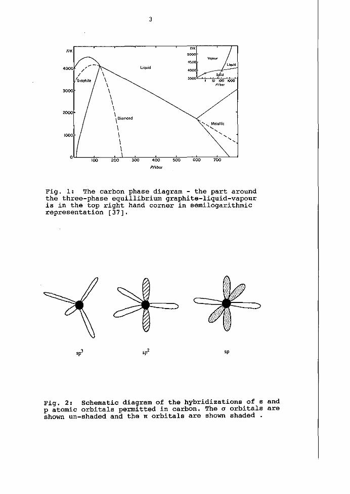
pressures (Fig. 1) [37], so that it exists under normalconditions only as a metastable phase. Although due to kinetic
reasons diamond remains unchanged at lower temperatures, at
about 1500 0C in an inert atmosphere begins its transformationinto the stable modification-graphite.
Since the first successful attempts to synthesize diamond
- those in Sweden [62,63] and USA [20], the laboratoryexperiments have been turned into an advanced industry. In theindustrial process a suitable carbon source (graphite) is
brought to the thermodynamically correct region in the presence
of a solvent/catalyst (one of the group VIII transition metals)whereby the diamond synthesis results.
In recent decades it has proved possible to produce
virtually pure carbon films with properties similar to those of
diamond by deposition from a gas phase at low pressures, usingmethods which provide activated, high energy species in the gas
phase. However, the films exhibited marked differences in their
optical, electrical, mechanical and other characteristics,depending on the method and conditions of preparation used.
This diversity of properties is a consequence of the ability
of carbon atom to form different strong carbon-carbon chemicalbonds.
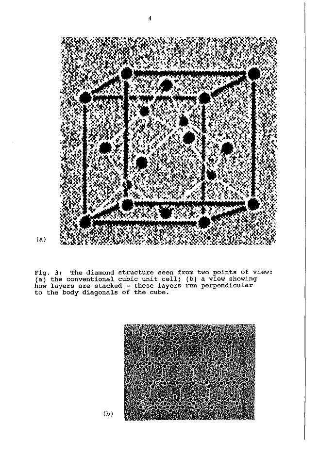
The nature of the bond formed is determined by the type
of hybridization of valence electrons (spl, sp2, sp3) (Fig. 2),
2
the particular chemical bond being determined by the overlap
of the electronic orbitals. The sp3 hybridization leads to
formation of four strictly directed strong covalent bonds with
a resulting tetrahedral coordination. This well-known structure
of diamond (Fig. 3) leads, in turn, to its isotropic properties.
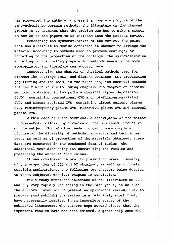
The sp2 hybridization, in which only three of the four
electrons of carbon atom are involved, leads to formation of
three coplanar, strictly directed, strong covalent bonds and to
the well-known hexagonal layer network of graphite. The fourth
(delocalized) electron is responsible for very weak forces
holding together the hexagonal layers (Fig. 4).
In consequence, graphite is, in contrast to diamond,
soft, black and electrical conductor. In addition, and again
in contrast to diamond, it is characterized by an exceptional
anisotropy of properties.
Under the conditions of deposition of carbon from a vapour
phase, simultaneous formation and coexistence of different
carbon/carbon bonds is virtually inevitable. Thus in
synthesizing diamond by this method, simultaneous formation of
sp2 bonds takes place. Therefore the product of deposition was
never "pure" diamond coating, but rather a "diamondlike" layer
containing, in addition to the sp3 bonds, greater or lesser
amount of graphitic material, i.e. the sp2-bonded carbon atoms.
After early successful attempts to grow diamond epitaxially,
i.e. with very low deposition rate, it is only in recent years
that it has become possible to deposit diamond layers at
acceptable and even high growth rates and yet without any
detectable amount of sp2 bonds and, therefore, with properties
close to those of natural diamond.
The aim of this study has been to present an up-to-date
condensed review of the rapidly progressing knowledge concerning
formation of diamond and diamondlike coatings by deposition of
carbon from a vapour phase. The study should help newcomers to
the field to rapidly orient themselves; it might also help those
working in the field to have an overall picture of the progress
made during the recent years.
It should be mentioned that, in contrast to the situation
with BN coatings [66] where the relative scarcity of literature
3
TIK '"eocoVopour
-toccLiquid
Uqwld.000
\.000
S9lid
\ "00 , 10 '00 ceo\ P/ba,
3000 \\\\
2000 \ .\ Diamond
.......... Merollic\ "- ,\
, ,\
-, ,\
100 200 300 .00 '00 600 700
Plkoo(
Fig. 1: The carbon phase diagram - the part aroundthe three-phase equillibrium graphite-liquid-vapouris in the top right hand corner in semilogarithmicrepresentation [37].
sp
Fig. 2: Schematic diagram of the hybridizations of sandp atomic orbitals permitted in carbon. The 0 orbitals areshown un-shaded and the IT orbitals are shown shaded .
4
(al
Fig. 3: The diamond structure seen from two points of view:(a) the conventional cubic unit cell; (b) a view showinghow layers are stacked - these layers run perpendicularto the body diagonals of the cube.
(b)
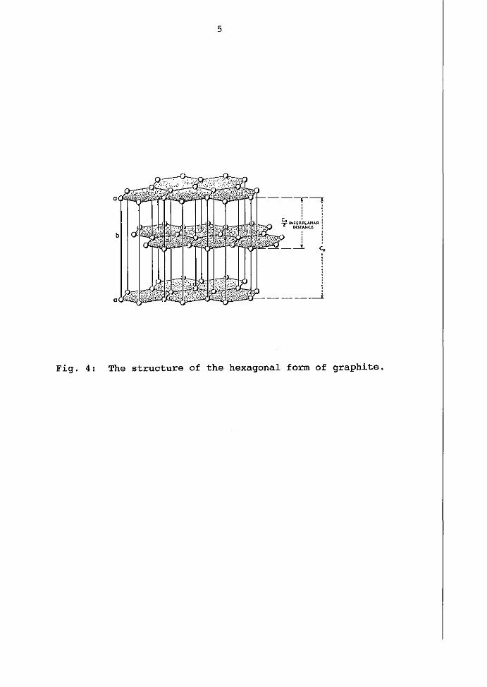
Fig. 4:
5
The structure of the hexagonal form of graphite.
6
has prevented the authors to preSent a complete picture of the
BN synthesis by certain methods, the literature on the diamond
growth is so abundant that the problem was how to make a proper
selection of the papers to be included into the present review.
Concerning the systematization of the review, the point
that was difficult to decide consisted in whether to arrange the
material according to methods used to produce coatings, or
according to the properties of the coatings. The systematization
according to the coating preparation methods seems to be more
appropriate, and therefore was adopted here.
Consequently, the chapter on physical methods used for
diamondlike coatings (DLC) and diamond coatings (DC) preparation
(sputtering and ion beam) is the first one, and chemical methods
are dealt with in the following chapter. The chapter on chemical
methods is divided in two parts - chemical vapour deposition
(CVD), containing conventional CVD and hot-filament-assisted
CVD, and plasma assisted CVD, containing direct current plasma
CVD, radiofrequency plasma CVD, microwave plasma CVO and thermal
plasma CVD.
Within each of these sections, a description of the method
is presented, followed by a review of the published literature
on the subject. To help the reader to get a more complete
picture of the diversity of methods, apparatus and techniques
used, as well as of properties of the materials obtained, these
data are presented in the condensed form of tables, the
additional text discussing and summarizing the results and
presenting the authors' conclusions.
It was considered helpful to present an overall summary
of the properties of OLC and DC obtained, as well as of their
possible applications, the following two chapters being devoted
to these subjects. The last chapter is conclusion.
The already mentioned abundance of the literature on OLC
and DC, very rapidly increasing in the last years, as well as
the authors' intention to present an up-to-date review, i.e. to
prepare (and publish) the review in a relatively short time,
have necessarily resulted in an incomplete survey of the
published literature. The authors hope nevertheless, that the
important results have not been omitted. A great help were the
7
recently published review articles covering some of the subjectstreated in the present review.
A problem of terminology has been a rather difficult one.
Because of the fact that structure and properties of coatings
obtained using the deposition methods depend on the method and
conditions of preparation used, these vary in a broad range.
The properties which have been reported for the coatings
prepared range from graphitelike (electrically conducting and
optically opaque) or polymerlike (electrically insulating, soft
and optically transparent) to diamondlike (electrically
insulating, very hard and optically transparent). Different
names which have been used to designate the prepared coatings
are diarnondlike carbon, i-carbon, ale, a-C:H, hard carbon, dense
carbonaceous. Different names have been often used to designate
coatings with similar properties.
The difficulty in defining criteria in order to
distinguish between polymerlike, diamondlike and diamond
coatings stems also from the fact that different researchers
have used different methods to characterize the coatings
prepared.
Therefore, the criteria adopted in this work and the
definitions of diamondlike and diamond coatings used are
somewhat vague.
DLC are carbon coatings for which the combination of the
methods of characterization used permits to conclude that, along
with presence of hexagonal graphite arrangement, they contain a
considerable proportion of carbon-carbon bonds with tetrahedral
coordination, making the coatings similar in their properties to
diamond.
Diamond coatings are nearly pure carbon coatings for which
a combination of methods used for characterization permits to
conclude that the carbon atoms of which they consist are in
tetrahedral coordination, with undetectable or insignificant
proportion of carbon atoms in the hexagonal graphite
arrangement, making properties of the coatings close to those
of diamond.
In addition to the well-known cubic diamond, four other
metastable carbon phases have been identified (lonsdaleite -
8
hexagonal diamond [37], chaoite - another hexagonal phase and
two other cubic phases [64,24]. All these phases are stable at
the proper high-pressure, high temperature conditions. However,
although the crystal structure of these phases was identified,
very little is known about their properties. In some papers
reporting diamondlike coatings preparation, one or more of these
phases have been formed. In the present review under the term
diamond we shall mean, unless otherwise stated, the well-known
cubic diamond.
9
2. PHYSICAL METHODS FOR PREPARATION OF DIAMOND AND
DIAMONDLIKE COATINGS
In physical methods of diamond and diamondlike coatingspreparation, no chemical changes are supposed to take place.
The methods which are included under this heading are sputtering
from carbon target and a group of methods which use ion beam
(IB) techniques for coating preparation (direct IB, massselected IB, IB sputtering and dual IB).
This classification is, however, only partly correct,
because in IB methods not only beams of carbon are used, butalso beams obtained by ionization of various hydrocarbonmolecules, which undergo different chemical changes in the
process of coating formation.
2.1 Sputtering
Sputtering is the emission of material particles fromsolid surfaces (target) which are bombarded with high energy
particles, usually Ar gas ions.
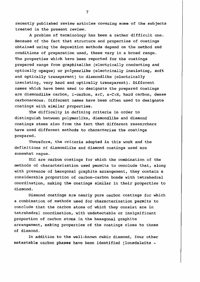
Diamondlike carbon films have been produced using directcurrent (de) planar magnetron sputtering of a graphite target
in ultrapure argon gas at a pressure of 10-2 mbar and at asubstrate temperature close to ambient temperature [98].
The target power was varied in the range 5-500 W (the targeteffective area was about 20 cm2).
The films prepared at low sputtering power are very dense(2.1-2.2 g/cm3), with electrical resistivity of 10 4 ohm cm and
hardness of 12-24 GPa. The films possess a very low optical gapas compared to the films obtained by other methods. The range
is 0.40-0.74 eV, meaning that the film is transparent in the
IR region. Analysis of their optical properties shows that the
films possessing the best DL properties consist principally oftetrahedrally sp3 bonded atoms with the sp3/sp2 coordination
of carbon atoms ratio equal to 3.1. As the sputtering power
increases, there is a sp3 to sp2 transition in the amorphous
10
carbon matrix, so that the films prepared at higher power
consist of approximately equal mixtures of sp3 and sp2
coordinated atoms.The authors conclude that the presence of hydrogen is not
strictly neccesary for obtaining stable tetrahedral bonding in
the amorphous carbon matrix, but that hydrogen does improve DL
properties by reducing the refractive index and increasing the
infrared optical transparency.
It is interesting to note that no paper reporting
preparation of DC and DLC by the well known cathodic sputtering
technique could be found. The amorphous carbon films prepared
using a commercial RF sputtering system [97,67] do not show any
diamondlike properties.
2.2 ION BEAM
Since Aisenberg and Chabot's paper describing preparation
of DLC by ion beam beam deposition [2], a number of researchers
in the world used this and related methods.
This rapidly growing field has resulted in many
publications, only some of which have been included in the
Table 1 (without the pretense that the best selection has been
made) .Several excellent review articles have been recently
published on the subject [4,64,77]. Other recent papers [50,79,
83,3] may help to get additional informations about ion beam
deposited carbon layers, and [113,116,40,115] are dealing with
the method and application in general.
Compared to other plasma sources, ion beams permit
a greater control of deposition parameters. They can have
a narrow energy distribution and specified direction, the
beam energy and ion current density being controlled almost
independently over a wide range of process conditions.
The advantage of this method in comparison with most plasma
techniques lies also in the fact that in the latter bombardment
conditions are controlled by a variety of parameters including
plasma power, gas pressure, gas composition, flow rate and
11
system geometry. Furthermore, the separation of the ion
generating plasma volume from the substrate minimizes
interaction between high energy plasma electrons and
the substrate, so that high energy particle interaction is
produced exclusively by the well-defined beam ions.
It follows from the above said that, in order to take full
advantage of the control offered by the ion beam deposition
techniques, it is important to maintain the ion beam energy,
current and chemical identity of the species while transporting
the beam to the substrate or target. In this regard, it is most
important to minimize the pressure in the region of beam
transport in order to prevent energy and spatial distribution of
the beam ions from extensive broadening due to their interaction
with background gas.
The pressure is usually 10-4 - 10-6 mbar, because in this
pressure range mean free path is sufficiently long and most of
the ions will maintain their energy (e.g. for a pressure of
about 1x10⁻⁴ mbar, 90% of the Ar+ ions can be expected to
maintain their charge for a distance of 10 cm downstream [4].
Furthermore, the substrate is most often kept at room
temperature or close to it, the energy of the beam ensuring the
necessary rearrangement of the atoms in the surface of the film.
The original Aisenberg and Chabot's method [2] was
a direct IB one, meaning that the ionized carbon atoms
were directly sent to the substrate and deposited on it.
Other methods, developed since include: a mass-selected (or
separated) IB, permitting to select from the initial beam the
desired ionic species; IB sputter deposition, where IB is used
to sputter the carbon atoms from a suitable carbon or graphite
target in order to effect their deposition on a near-by
substrate; dual ion beam in which first beam is used either as
a direct IB transporting carbon or carbon-containing ions to the
substrate, or to sputter carbon atoms from a target which are
then deposited, the second beam being used to bombard the
substrate in order to improve the coating properties. In
a variant of the dual beam method, a laser beam or magnetron
can be used to vaporize carbon from the target instead of lB.
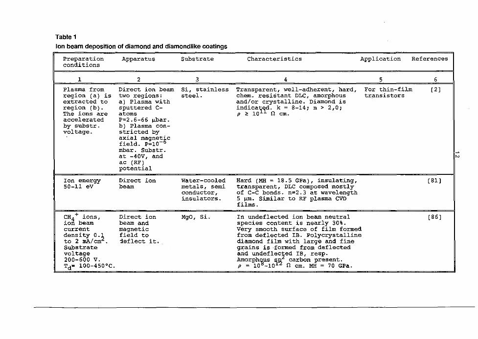
Table 1
Ion beam deposition of diamond and diamondlike coatings
N
Preparation Apparatus Substrate Characteristics Application Referencesconditions
1 2 3 4 5 6
Plasma from Direct ion beam 8i, stainless Transparent, well-adherent, hard, For thin-film [2)region (a) is two regions: steel. chern. resistant OLe, amorphous transistorsextracted to a) Plasma with and/or crystalline. Diamond isregion (b). sputtered C- indiCa\~d. k = 8-14; n > 2,0;The ions are atoms p ~ 10 n em,accelerated P=2.6-66 I'bar.by substr. b) Plasma con-voltage. stricted by
axial magnettcfield. P=10-moar . Substr.at -40V, and I
ac (RF)potential
Ion energy Direct ion Water-cooled Hard (MH = 18.5 GPa) , insulating, [81)50-11 eV beam metals, semi transparent, DLe composed mostly
conductor, of C-C bonds. n=2.3 at wavelengthinsulators. 5 um, Similar to RF plasma CVD
films.
C + . Direct ion MgO, Si. In undeflected ion beam neutral [86)H4 loons,ion beam beam and species content is nearly 30%.current magnetic Very smooth surface of film formeddensity 0'2 field to from deflected lB. Polycrystallineto 2 rnA/em . :Ieflect it. diamond film with large and fineSubstrate g~ains is -formed from deflectedvoltage and undeflec1ed IB, resp.200-600 V. Amorph~Us i~ carbon present.Td= 100-450°C. P = 10 -10 n em. MH = 70 GPa.
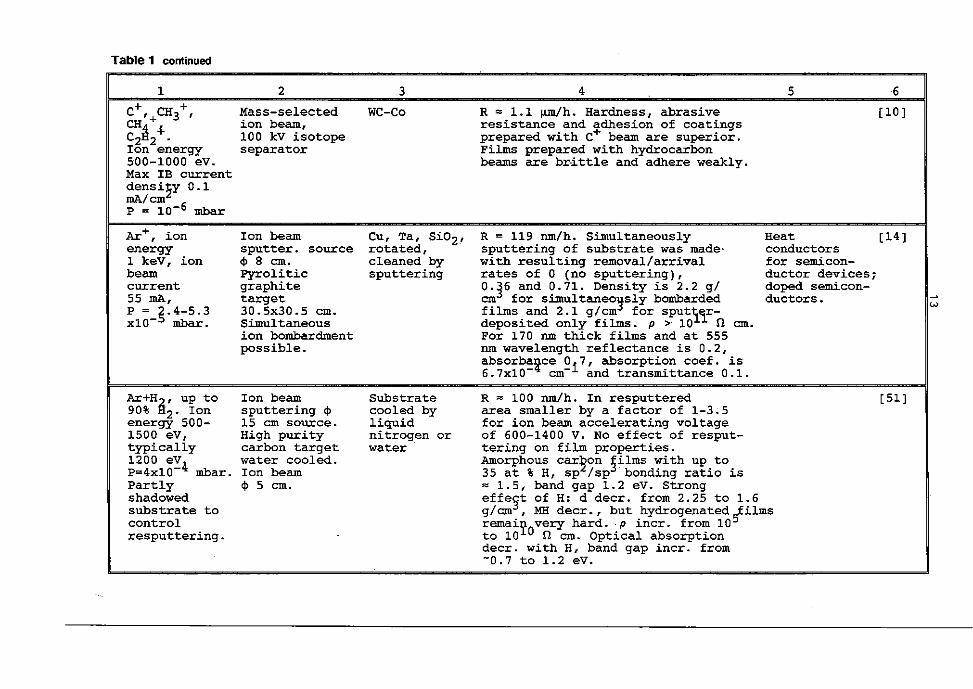
Table 1 continued
Co>
1 2 3 4 5 6+ + Mass-selected WC-Co R = 1.1 IllIl!h. Hardness, abrasive [10]C , CH3 I
CH+ ion beam, resistance and adhesion of coatingsC2~2+· 100 kV isotope prepared with C+ beam are superior.Ion energy separator Films prepared with hydrocarbon500-1000 eV. beams are br~ttle and adhere weakly.Max IB currentdensiZy 0.1rnA/emP = 10-6 mbar
Ar+ , ion Ion beam Cu, Ta, Si02.1 R = 119 nm/h. Simultaneously Heat [14 ]energy sputter. source rotated, sputtering of substrate was made- conductors1 keV, ion <l> 8 em. cleaned by with resulting removal/arrival for semicon-beam Pyro1itic sputtering rates of 0 (no sputtering), ductor devices;current graphite 0.j6 and 0.71. Density is 2.2 gl doped semicon-55 rnA, target em for simu1taneo~sly bombarded ductors. ,P = ~.4-5.3 30.5x30.5 em. films and 2.1 g/cm for sput\1r-xl0- mbar. Simultaneous deposited only films. p > 10 n em.
ion bombardment For 170 nm thick films and at 555possible. nm wavelength reflectance is 0.2,
absorb~ce °17, absorption ccef. is6.7xlO- cm- and transmittance 0.1.
Ar+Hg, up to Ion beam Substrate R = 100 nm/h. In resputtered [51]90% 2. Ion sputtering <l> cooled by area smaller by a factor of 1-3.5energy 500- 15 em source. liquid for ion beam accelerating voltage1500 eV, High purity nitrogen or of 600-1400 V. No effect of resput-typically carbon target water tering on film properties.1200 eV
4water cooled. Amorphous car~on ~ilms with up to
P=4x10- mbar. Ion beam 35 at % H, sp Isp bonding ratio isPartly <I> 5 em. :=::< 1.5, band gap 1.2 eV. Strongshadowed effe§t of H: d decr. from 2.25 to 1.6substrate to g/em , ME deer., but hydrogenated rfilmscontrol remaiYovery hard . . p incr. from 10resputtering. to 10 n em. Optical absorption
deer. with H, band gap incr. from-0.7 to 1.2 eV.
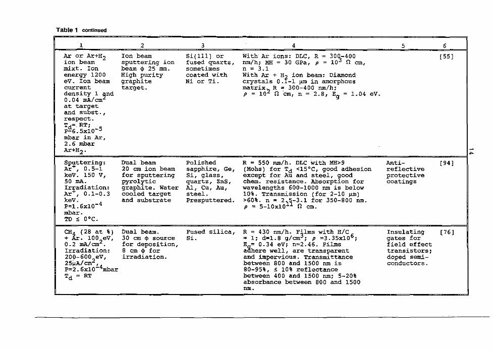
Table 1 continued
1 2 3 4 5 6
Ar or Ar+H2 Ion beam Si(lll) or With Ar ions: DLC, R = 30~-400 [55]ion beam sputtering ion fused quartz, nm/h; MH = 30 GPa, p = 10 n cm,mixt. Ion beam <I> 25 nun. sometimes n = 3.1energy 1200 High purity coated with With AI + Hi ion beam: DiamondeV. Ion beam graphite Ni or Ti. crystals O. -1 ~ in amorphouscurrent target. matrix~ R ": 300-400 nmlh;density 1 ~nd p = 10 n cm, n = 2.8, Eg = 1.04 eV.0.04 rnA/emat targetand subst.,respect.Td= . RT;P=6.5x10⁻⁵mbar in Ar,2.6 mbarAr+H2·
Sputtering: Dual beam Polished R = 550 nm/h. DLC with MH>9 Anti- [94]Ar+, 0.5-1 20 em ion beam sapphire, Ge, (Mohs) for Td <15°C, good adhesion reflectivekeV. 150 V, for sputtering Si, glass, except for Au and steel, good protective50 mAo pyro1ytic quartz, ZnS, chem. resistance. Absorption for coatingsIrradiation: graphite. Water AI, Cu, AU, wavelengths 600-1000 nm is belowAr+, 0.1-0.3 cooled target steel. 10%. Transmission (for 2-10 ~)
keV. and substrate Presputtered. >60%. n = 2 l1-3.1 for 350-800 nm.P=1.6x10- 4 p = 5-10x10 n em.mbar.TD S O°C.
CHt, (28 at %) Dual beam. Fused silica, R = 430 nmlh. F~lms with H/c Insulating [76]+ • 100
2ev,30 em <I> source Si. = 1; d=1.8 g/em , p =3.35x10 6, gates for
0.2 mA/em . for deposition, E = 0.34 eV, n=2.46. Films field effectIrradiation: 8 em <I> for a~ere well, are transparent transistors;209-6002ev, irradiation. and impervious. Transmittance doped semi-251lA/cm , between 800 and 1500 nm is conductors.P=2.6x10⁻⁴mbar 80-95%, S 10% reflectanceTd = RT between 400 and 1500 nm; 5-20%
absorbance between 800 and 1500nm.
...
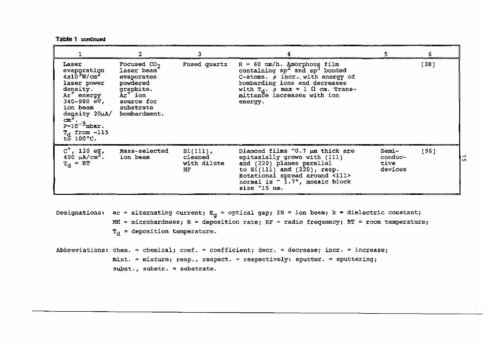
Table 1 continued
'J'
1 2 3 4 5 6
Laser Focused CO2 Fused quartz R = 60 nm/h. ~orphou3 film [38Jevap~rati~n laser beam containing sp and sp bonded4xlO W/crn evaporates C-atoms. p j.~cr." with energy oflaser power powdered bombarding ions and decreasesdensity. graphite. with Td" P max ~ 1 n em. Trans-Ar+ energy Ar+ ion mittance increases with ion340-980 eV, source for energy.ion beam substratedellsity 20pA/ bombardment.cm .P=10-5mba r.Td from -115to 100°C.
+ Mass-selected Si(ll1) , Diamond films -0.7 ~ thick are Semi- [96JC f 120 e¥,400 IJA/crn . ion beam cleaned epitaxially grown with (111 ) conduc- ,Td = RT with dilute and (220) planes parallel tive
HF to Si(ll1) and (220), resp. devicesRotational spread around <111>normal is - 1.7°, mosaic blocksize ....15 run.
Designations: ac
MH
Td
alternating current; £g = optical gap; IB = ion beam; k = dielectric constant;
microhardness; R = deposition rate; RF = radio frequency; RT = room temperature;
deposition temperature.
Abbreviations: chern. = chemical; coef. = coefficient; deer. = decrease; incr. = increase;
mdxt. = mixture; resp., respect. = respectively: sputter. ~ sputtering;
subst., substr. = substrate.
16
Each method has its varieties. Table 1 contains examples
of the mentioned methods.
Direct ion beam
In this method an ion beam of controlled composition,
energy and flux is directed onto a substrate. The impacting
ions are used to supply both the deposition atoms and the
energy required for improved film formation.
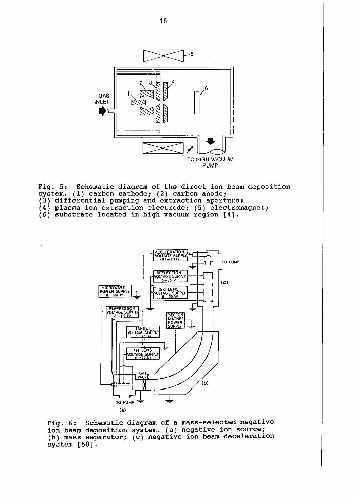
The original Aisenberg and Chabot's apparatus (2) is
represented schematically in Fig. 5. There are two vacuum
regions (a high-pressure one and low-pressure one) separated
by a plasma constrictor opening used for differential pumping.
The diameter of the constrictor opening is about 1.5 rom.
The plasma source chamber is the smaller one where the higher
pressure discharge (about 2.6x10⁻³ to 65x10-3 mbar) is used to
form the positive ions of materials such as carbon.
The discharge in the source chamber is used to introduce
the carbon atoms into plasma where the high-energy electrons
can ionize them. A hollow cavity in a carbon electrode is used
as one electrode and a carbon post in the center is used as the
other. Positive-ion bombardment is able to sputter carbon from
the electrode into the source plasma.
Both electrodes in the deposition source chamber are made
of carbon to reduce contamination. An axial magnetic field is
used to modify the electron orbits so that the discharge can
operate at lower pressures. The ions are extracted from the
source chamber by means of an auxiliary discharge drawn to an
anode located in the deposition chamber.
A constrictor is used to separate the source chamber and
the deposition chamber and to permit differential pumping so the
deposition chamber pressure can be maintained at 10-6 mbar. The
auxiliary discharge is designed so that use is made of the axial
magnetic field to direct the extracted plasma and to reduce the
space-charge spreading of the beam. By means of the extraction
arc, one has a low-pressure discharge (in the deposition
chamber) in series with the higher-pressure arc in the source
chamber.
17
In order to reduce film contamination, carbon inserts are
used in the constrictor and in the extractor anode.
The plasma in the deposition chamber can act as a source
of carbon ions as well as a source of electrons. A negative
potential applied to the substrate is used to attract the
positive ions. When insulating film are deposited, then an ac
or RF potential is applied to the substrate to attract the
necessary electrons for cancellation of the positive-ion
surface charge. The ion energy incident upon the substrate
can be adjusted by the substrate potential and by the amplitude
of the ac signal.
Before deposition, the substrate is cleaned by sputtering
for several minutes at -400 V; most of the substrate deposition
occurred at about -40 V. The ion current to the substrate is
approximately proportional to the extracted arc current. Film
deposition rates of about 18 ~m/h were obtained.
Mass-selected ion beam
Greater control is afforded by the use of mass-selected
IB deposition, in which the beam is prefiltered by a mass
separator. This technique permits precise control over the beam
species and allows deposition in ultra high vacuum conditions
which minimize surface contamination.
Fig. 6 contains schematical representation of a mass
selected IB apparatus (for negative C ions) [50].
The acceleration voltage of the deposited negative ion
beam was varied from 10 to 1000 V for a C- ion beam and from
40 to 400 V for C2- ion beam. The deposited area was about
1 cm2, the current density of the deposited ion beam was
30-100 ~A/cm2, and the deposition time was 1-2 h. The background
pressure in the deposition chamber was around 9xlO- 7 mbar during
deposition. Substrates used were n-type silicon wafers with
(100) plane and the resistivity of the wafers was 8-15 ohm em.
This method permits preparation of extremely pure films.
Its disadvantages are relatively low deposition rate, high cost
of the sophisticated mass-selected IB apparatus and, at least
in the existing systems, small size of the IB «3 cm2).
18
I><f-s
GASINLET..
TO HIGH VACUUMPUMP
Fig. 5: Schematic diagram of the direct ion beam depositionsystem. (1) carbon cathode; (2) carbon anode;(3) differential pumping and extraction aperture;(4) plasma ion extraction electrode; (5) electromagnet;(6) substrate located in high vacuum region [4] .
MICROWAVEPOWER SUPPLY
o-lOa 'II
. ACCELERATION •VOlTAGE SIPPLV
-01- -vTO PUMP
(e)
(a)
Fig. 6: Schematic diagram of a mass-selected negativeion beam deposition system. (a) negative ion source;(b) mass separator; (c) negative ion beam decelerationsystem [50].
19
This may restrict utilization of this method to some special
applications.
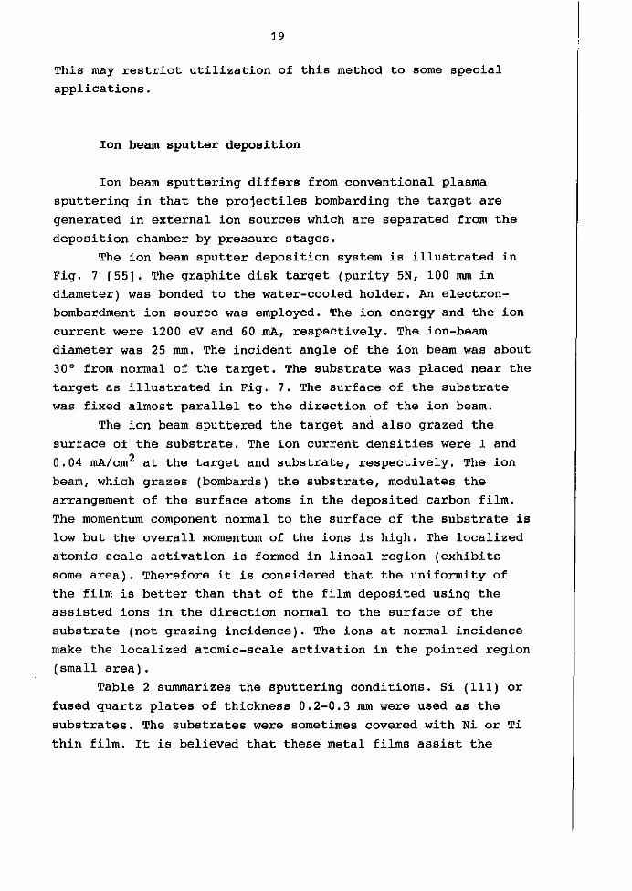
Ion beam sputter deposition
Ion beam sputtering differs from conventional plasma
sputtering in that the projectiles bombarding the target are
generated in external ion sources which are separated from the
deposition chamber by pressure stages.
The ion beam sputter deposition system is illustrated in
Fig. 7 [55]. The graphite disk target (purity 5N, 100 rom in
diameter) was bonded to the water-cooled holder. An electron
bombardment ion source was employed. The ion energy and the ion
current were 1200 eV and 60 rnA, respectively. The ion-beam
diameter was 25 rom. The incident angle of the ion beam was about
30° from normal of the target. The substrate was placed near the
target as illustrated in Fig. 7. The surface of the substrate
was fixed almost parallel to the direction of the ion beam.
The ion beam sputtered the target and also grazed the
surface of the substrate. The ion current densities were 1 and
0.04 rnA/cm2 at the target and substrate, respectively. The ion
beam, which grazes (bombards) the substrate, modulates the
arrangement of the surface atoms in the deposited carbon film.
The momentum component normal to the surface of the substrate is
low but the overall momentum of the ions is high. The localized
atomic-scale activation is formed in lineal region (exhibits
some area). Therefore it is considered that the uniformity of
the film is better than that of the film deposited using the
assisted ions in the direction normal to the surface of the
substrate (not grazing incidence). The ions at normal incidence
make the localized atomic-scale activation in the pointed region
(small area).
Table 2 summarizes the sputtering conditions. Si (Ill) or
fused quartz plates of thickness 0.2-0.3 rom were used as the
substrates. The substrates were sometimes covered with Ni or Ti
thin film. It is believed that these metal films assist the
20
nucleation of the diamond. The substrate was not heated and kept
at room temperature.
Table 2
Sputtering conditions for film preparation [55]
Target
Target dimension
Ion source: Energy
Current
Beam apertureGas pressure
Target-ion source spacing
Growth rate
Graphite plate
100 mm in diameter
1200 eV
60 rnA
25 mm in diameter6.5xlO-5 mbar
250 mm
300-400 nm/h
The advantage of this method is that because of high
vacuum it produces pure carbon films (if the target material
is made of pure carbon). In addition, it is often possible to
bombard simultaneously the growing film on the substrate by the
ions from the beam, which may affect properties of the film.
The disadvantage is low deposition rate.
Dual ion beam
By using two different ion beam sources, a better control
of the deposition and sputtering conditions is ensured.
The apparatus is shown in Fig. 8 [40]. Two ion beams
sources of the Finkelstein type are attached to a deposition
chamber in such a way that one source is used to produce a flux
of sputtered particles from a solid target while the other
source allows the growing film to be bombarded with inert or
reactive ions of variable energy.
The target was pyrolytic graphite and was sputtered with
argon ions of energies 0.5-1 keV. A second source irradiated the
growing films with 0.1-0.3 keV Ar+. The optics in the primary
source are focusing tungsten grids; those in the co-bombarding
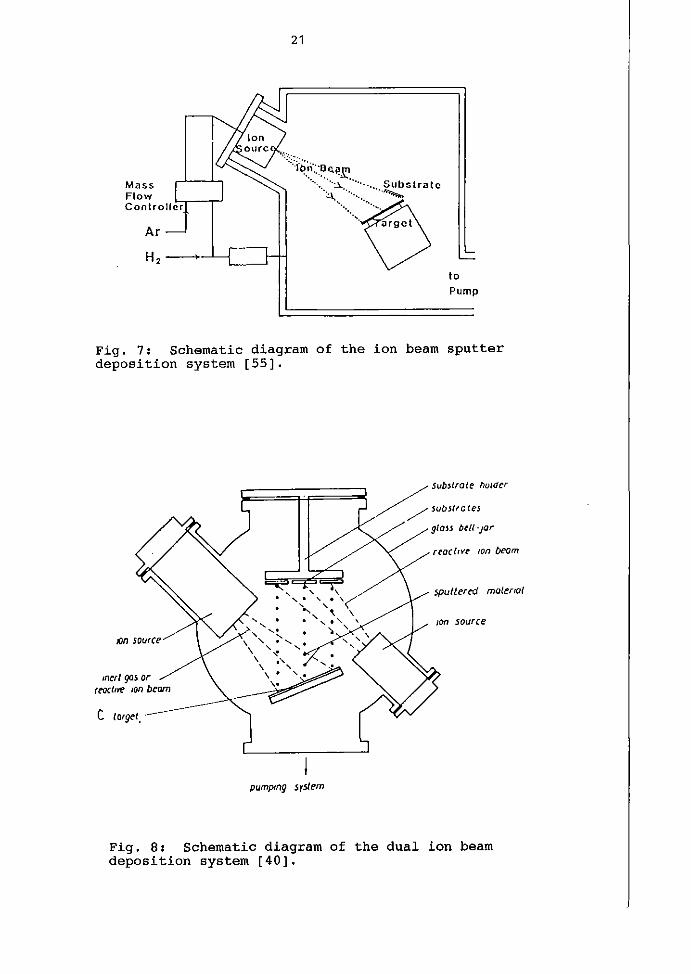
H, --->
21
I~.n·::~ ~~R'...... >..: Subslrate'«::e
toPump
Fig. 7: Schematic diagram of the ion beam sputterdeposition system [55].
on source
Inert gas or,eoelll!' Ion beam
C Wgel.·
/ Substrate holder
/ -: wostrctes
glass btll-Jor
reactsve Ion beam
5{Jutt.erro ma/enal
Ion source
pumping sy5tem
Fig. 8: Schematic diagram of the dual ion beamdeposition system [40].
22
source are graphite. Metallic contamination in the deposited
films was minimized by the graphite grids and by covering metal
parts with graphite shields. Table 3 summarizes the operating
parameters [94].
Table 3
Operating parameters for optimum transparent carbon filmsdeposition bythe dual ion beam technique
Sputtering source
Ar pressure
Presputter
Sputter
Co-bombarding source
Ar pressure
Presputter
Deposition
Chamber pressure
Deposition rate
Maximum substrate temperature
Target and sample angles to beams
Focused 20 cm Kaufman-type3.7x10-4 mbar
600 V, 700 rnA, 5 min
850 V, 840 rnA, neutralized
10 cm Kaufman-type2.7x10- 4 mbar
150 V, 100 rnA, 3 min
150 V, 50 rnA
1.2x10⁻⁴ mbar
550 nm/hS OOC
45°
Influence of ion beam deposition parameters on the film
properties
Ion energy is the primary parameter determining the
properties of the carbon films, inducing the formation of
dense, adhering, hard carbon films.
The ion energy range is rather wide and extends from
10 eV to 1.5 keY.
In the direct ion beam methods this range is usually from
40 to several hundred eV [4], although energies up to 1 keY have
been used for ionized molecule beams [116]. For mass-selected IB
the energy range from 10 eV to 1 keY is used [64]. For the
23
method using sputtering of the target material higher energies,
up to 1.5 keY are used. These energies provoke an enhanced
mobility of the atoms on the film surface, as well as their
shallow implantation, but they also cause a preferential
sputtering of the sp2 bonded atoms.
Incident flux and angle of incidence are parameters
influencing the film properties directly and indirectly
through secondary effects.
In the simplest set-up in the direct ion beam method,
in which the substrate is located directly within the beam
transport region, the bombarding ions are non selectively
extracted from the ion-source plasma. The beam is then a
combination of inert gas, deposition atoms, clusters,
molecular fragments, etc.
In order to achieve better control of ion beam
composition, magnetic field was used to deflect the beam
(CH4+ ions), thus avoiding the neutral species (amounting
to about 30%) and improving the film properties [86].
The best control of ion beam composition is achieved
using mass-selected methods.
The ion bombardment of the deposited film, as used in
dual-beam and (sometimes) sputtering methods is believed to
increase the diamondlike component by giving surface atoms
extra kinetic energy to move into sp3-bonded sites, and by
preferential removal by sputtering of amorphous or sp2-bonded
domains [4].
Species used for carbon deposition include carbon ions
(negative and positive), hydrocarbon radicals, carbon cluster
ions (Cn+) and non-carbon species such as hydrogen and argon.
In most carbon deposition processes there is an unidentified
mixture of several species.
Deposition from hydrocarbon species results in a high
conceptration of hydrogen in the films. Argon ions are used in
most "ion-assisted" processes (e. g. IB sputtering). Argon is
believed to preferentially sputter graphitic and amorphous
( Sp2) carbon, enriching the diamond (Sp3) constituent of the
film [64]. Hydrogen is believed to stabilize the sp3 carbon by
24
saturating dangling bonds and by preferentially etching sp2carbon.
The properties of the ion beam deposited films depend onthe process parameters used.
Composition and properties of the films depend on the ion
beam composition. carbon ions produce pure (hydrogen-free)
carbon films (DLC) and hydrocarbon ions produce hydrogen
containing carbon films (H-DLC). Hydrogen content and properties
of H-DLC are nearly independent on the type of hydrocarbon, but
depend strongly on their composition, as well as on ion energy.
The virtual independence on hydrocarbon type is explained
(4) by hydrocarbon disintegration upon surface impact if the ion
energy is on the order of 100 eV.
The films are predominantly amorphous, but can have
extensive sp3-bonded short-range order [64,4]. However, poly
crystalline diamond films can also be formed with crystallites
up to 5 ~m [4,86), so that the range from amorphous to the well
crystalline coatings is covered.
The films are chemically inert to all known solvents.
Both "pure" (DLC) and hydrogen-containing (H-DLC) films have
been deposited on many different substrates: glass, quartz, Si,
NaCl, KCl, CaF 2, Ge, plastics, steel, other metals, nylon, paper
and other. DLC display the highest adhesion to carbide-forming
substrates (Si, Ge, Mo, W), but they adhere well to most
substrates if these are properly cleaned by ion bombardmentprior to deposition.
According to (64), the sp3 films are deposited on
substrates held at TdS70°C in the mass-selected IB method,
while graphitic films are obtained at Td~lOOoC. The explanation
offered is that under proper temperature conditions, energetic
carbon ions displace preferentially sp2 atoms, leaving the
sp3 atoms in their positions, but also that the host diamond
matrix imposes the bonding type of the deposited carbon
( "mold" effect).
Although similar'experimental results have been obtained
by other authors, a recent paper (86) in which polycrystalline
diamond has been reported at Td=100-450°C should be mentioned.
The density is typically about 2.4 g/cm3 for pure carbon,
25
and 1.8 g/cm3 for hydrogen-containing films.
Although the thin (100 nm) films are apparently stress
free, thicker films tend to separate from the substrate,
probably due to internal compressive stress.
Both ion-beam OLC and H-OLC are unusually smooth, often
smoother than the substrate. Thin films reproduce the morphology
of the substrate [103].
The resistivity of OLC is on the order of 10 11_1012
ohm cm, while H-OLC have resistivity in the range 10 7_10 16 ohm
em, increasing with increasing H content.
Breakdown voltage of OLC is about 1x10 6 V/cm, and
. dielectric constant is about 8.
The OLC are optically transparent. IR absorption of both
OLC and H-OLC in the 1-10 ~m wavelength range is very low,
except at wavelengths where C-H vibrations appear.
The index of refraction is ~2 in the visible and IR parts
of spectrum for both OLC and H-OLC. Very high values (up to 3.1,
see Table 1) have also been reported.
In general, the advantages of the ion beam methods are
that diamondlike or diamond films can be formed under controlled
deposition conditions on the substrate surface made of various
materials at the ambient temperature. However, since accelerated
ions are employed, the formed diamond has many defects and it is
difficult to obtain diamonds having good crystallinity.
Furthermore, the deposition rate is intrinsically low because
the ion beam density can not be substantially increased.
Combination of properties of ion-beam-deposited OLC
and H-OLC (transparency, electrical insulation, high breakdown
voltage, high thermal conductivity, chemical resistance, barrier
properties, hardness, good adhesion to substrates, smoothness,
wear resistance), together with the fact that they can be
deposited at temperatures slightly above room temperature,
have led to their application.
An initial application for the transparent diamondlike
films were protective coatings for plastic lenses, while OLC of
controlled thickness have been used to improve transmission of
Ge IR optics [4].
26
However, wider application of IB deposited coatingsremains a challenge. This may include, in addition to various
optical elements (for high power lasers, for mirrors and
windows, optical sensors, decorative jewellery or silverware),
electronic devices (field effect transistors, semiconductors),
high power or high power density devices, protective coatings
for use in biomedical applications and fiberoptics, for
cutting tools etc.
Nevertheless, for all these and many other possible
applications, the coatings prepared by ion beam methods will
have to resist a competiton with coatings obtained by other,
cheaper methods.
27
3. CHEMICAL METHODS FOR PREPARATION OF DIAMOND AND
DIAMONDLIKE COATINGS
3. 1 CHEMICAL VAPOUR DEPOSITION
3.1.1 Conventional chemical vapour deposition
Since at low pressure (and temperatures) the thermo
dynamically stable modification of carbon is graphite, the
question is whether, and if so, how diamond can be produced
under non-equilibrium conditions. The factors which determine
the modification that will be produced during the pyrolysis of
a hydrocarbon are, in addition to pressure and temperature,
composition of the gas phase, nature of the hydrocarbon used for
pyrolysis and availability of a diamond surface. The first three
parameters determine how far from the equilibrium heterogeneous
reactions of formation of diamond and graphite will take place.
Theoretical studies show [105] that in the simplest case
of growing diamond from supersaturated carbon vapour there is a
certain optimum supersaturation (i.e. ratio piPe' where P is the
optimum pressure and Pe is the equilibrium vapour pressure over
diamond) at which the ratio of probabilities of formation of
two-dimensional nuclei of diamond and graphite will be maximum.
At this supersaturation the unavoidable covering of the growing
diamond surface with graphite growth centres will be minimal.
However, under these conditions the diamond growth rate would be
too low, so that in order to increase it only to the lower limit
which allows its experimental detection (about 0.1 nm/h), it is
necessary to operate at much higher supersaturations, where
graphite evolution becomes considerable.
Availability of diamond surface is certainly a factor
which would favorize the diamond growth. As to the nature of the
hydrocarbon used, the obvious factor which should influence
graphite or diamond formation would be the type of bonds, the
tetragonal bonds being favorable for diamond growth.
28
Remains gas phase composition, the factor which finally
permitted to solve the problem of pure diamond growth under
non-equilibrium conditions.
Various experiments have been designed with the aim of
preparing diamond, many of them trying to solve the problem
using difference in kinetics of formation of diamond and
graphite. One such approach is based on a difference in kinetics
of formation of diamond and graphite nuclei in the pulse
crystallization [105]. In this method synthesis of diamond on
diamond seed crystals is effected from hydrocarbon gases, using
a periodical (pulse) change in supersaturation.
The time of formation of a critical (stable) diamond
nucleus should be shorter than the corresponding time for
graphite because of the orientation effect of the diamond
substrate. With suitably chosen pulse duration, the diamond
nuclei will reach the critical size and the graphite nuclei
will remain subcritical. Therefore, the unstable (subcritical)
graphite nuclei will disappear during pauses between the pulses
when supersaturation decreases, but the stable diamond nuclei
will remain and continue to grow during the next pulse.
Systematic research work on the growth of diamond in the
region of its thermodynamic metastability has independently and
almost simultaneously started in the USSR and USA in the second
half of 1950's [105].
Already in 1956 Spitsyn and Derjaguin succeeded in
building up local areas of a· natural diamond single crystal face
through thermal decomposition of gaseous CBr4 and CJ 4 under low
pressures «10-3 mbar) and at a temperature of about 900°C
[105].
The Eversole's patent [35] filed in 1958 describes the
growth of diamond on the diamond seed crystals by pyrolysis of
methane at low pressure (optimum range 0.20-2.6 mbar) and low
temperature (optimum range 1000-11000C). Weight gain with
respect to initial weight of the seed crystals was up to
0.76%/h. The pyrolysis was periodically interupted in order
to remove graphite which was simultaneously deposited, using
prolonged heating in hydrogen at 1000-1100 oC under 10-50 bar.
Instead of methane, methyl-group-containing compounds could
29
be used, but benzene, CC14 and hydrocarbons not containing
methyl groups did not produce diamond.
The diamond deposition was found to continue even after
considerable black carbon had been deposited.
Another paper [8] describing diamond formation by thermal
decomposition of methane used similar conditions to those of
Eversole (lOSO°C, 0.4 mbar). Methane was passed continously over
diamond seed crystals. The obtained deposits on the diamond
crystals (up to 23.7 wt% mass increase) were analysed by a
number of methods (chemical analysis, chemical etching, density
measurements, X-ray and electron diffraction, microwave
absorption, electron spin resonance and visual observations).
The authors consider that the evidence presented demonstrates
conclusively that diamond has been formed.
Thus, growth of diamond by CVD has been shown to be
possible. However, growth rate of diamond is low and the method
suffers from an unavoidable deposition of graphitic carbon which
must be removed by tedious procedures.
Nevertheless, after these experiments a number of
researchers have studied various aspects of diamond formation.
However, the most important problem of avoiding simultaneous
deposition of graphitic carbon was solved only recently.
Probably the most effective approach to obtain selective
growth of diamond consists in etching the non-diamond carbon
directly during the diamond film growth by introducing into the
gas phase an etching or purifying gaseous agent. Although oxygen
or other oxidising agents may be used [105], the methods using
atomic hydrogen have been applied most extensively because of
high reactivity of hydrogen and the fact that it reacts strongly
with graphite, but practically does not affect diamond [8].
This highly selective etching of graphite, is illustrated in
Fig. 9 .lIOS]. Thus, even if the growth rates of diamond and
graphite differ insignificantly (as represented in Fig. 9),
the overall effect will be growth of diamond, and total absence
of graphitic carbon.
Such a method has been described in [104] using a
"chemical transport method". Fig. 10 represents an apparatus for
the chemical transport [105]. The gas containing hydrocarbons
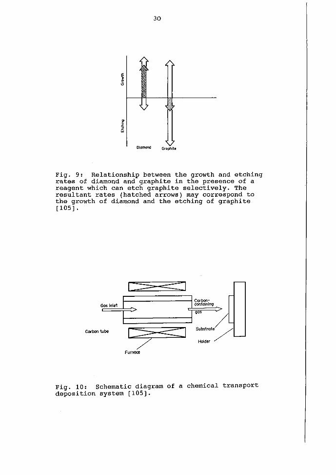
30
,~
<
I~
,
~:<
~
01"""""V
Graphite
Fig. 9: Relationship between the growth and etchingrates of diamond and graphite in the presence of areagent which can etch graphite selectively. Theresultant rates (hatched arrows) may correspond tothe growth of diamond and the etching of graphite[105] .
Gos inlet
'as
Corbon tube 1=:37Furnace
-<:1 SUbstrate/
Holder
Fig. 10: Schematic diagram of a chemical transportdeposition system [105].
31
(CH4, C2H6, C2H4, C2H 2) formed by reaction of graphite with
hydrogen at high temperature is transported to the diamond
substrate. A superequilibrium concentration of atomic hydrogen
obtained from H2 gas either by heating (several % H), or byelectric discharge (about 10% H) was introduced in order to
remove the graphitic carbon formed. At a substrate temperature
between 800 and 1200°C (the optimum temperature resulting in the
highest growth rate being 1000°C) a pure diamond was obtained
(without graphitic carbon) which could not be graphitized in
vacuum at 1500°C, in contrast to the diamondlike carbon.
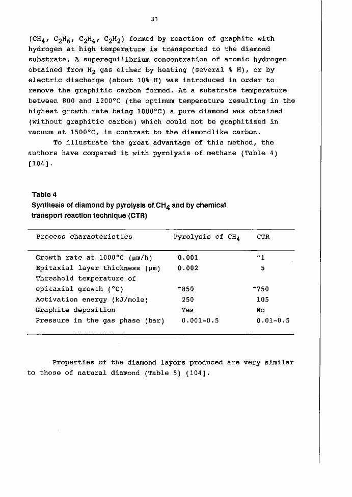
To illustrate the great advantage of this method, the
authors have compared it with pyrolysis of methane (Table 4)
[104] .
Table 4
Synthesis of diamond by pyrolysis of CH4 and by chemicaltransport reaction technique (CTR)
Process characteristics
Growth rate at 10000C (~m/h)
Epitaxial layer thickness (~m)
Threshold temperature of
epitaxial growth (OC)Activation energy (kJ/mole)
Graphite deposition
Pressure in the gas phase (bar)
Pyrolysis of CH4
0.001
0.002
N850
250
Yes
0.001-0.5
CTR
Nl
5
N750
105
No
0.01-0.5
Properties of the diamond layers produced are very similar
to those of natural diamond (Table 5) [104].
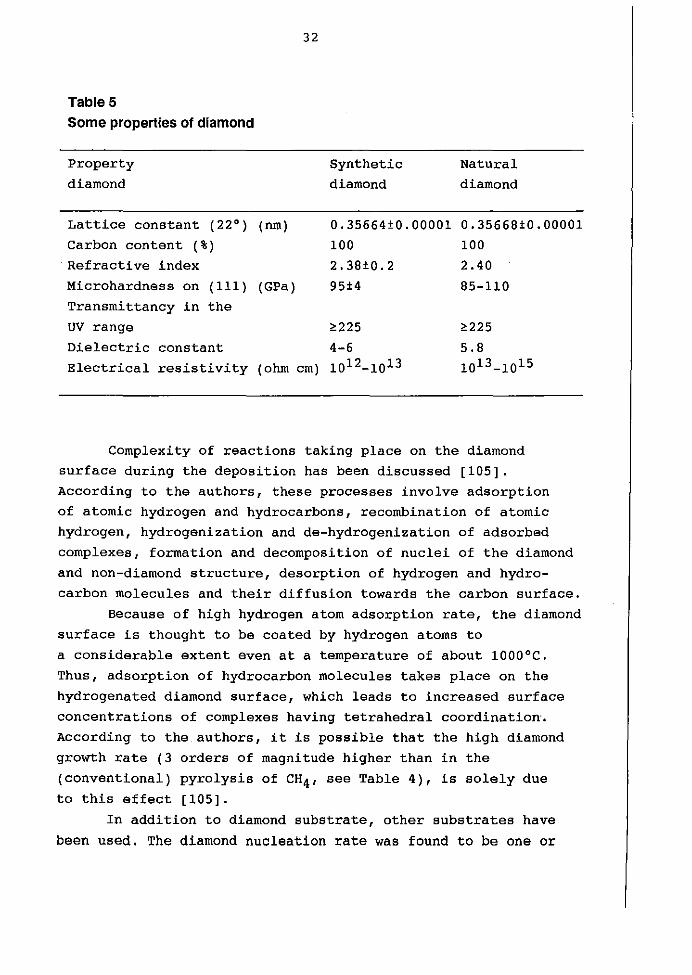
32
Table 5
Some properties of diamond
Property
diamond
Synthetic
diamond
Natural
diamond
~225
5.81013_1015
0.35668±0.00001
100
2.40
85-110
~225
0.35664±0.00001
100
2.38±0.2
95±4
(nrn)
4-6(ohm ern) 10 12_1013
Lattice constant (22°)Carbon content (%)Refractive index
Electrical resistivity
Microhardness on (Ill) (GPa)
Transmittancy in the
UV range
Dielectric constant
Complexity of reactions taking place on the diamond
surface during the deposition has been discussed [105].
According to the authors, these processes involve adsorption
of atomic hydrogen and hydrocarbons, recombination of atomic
hydrogen, hydrogenization and de-hydrogenization of adsorbed
complexes, formation and decomposition of nuclei of the diamond
and non-diamond structure, desorption of hydrogen and hydro
carbon molecules and their diffusion towards the carbon surface.
Because of high hydrogen atom adsorption rate, the diamond
surface is thought to be coated by hydrogen atoms to
a considerable extent even at a temperature of about 1000°C.
Thus, adsorption of hydrocarbon molecules takes place on the
hydrogenated diamond surface, which leads to increased surface
concentrations of complexes having tetrahedral coordination.
According to the authors, it is possible that the high diamond
growth rate (3 orders of magnitude higher than in the
(conventional) pyrolysis of CH4, see Table 4), is solely due
to this effect [105].
In addition to diamond substrate, other substrates have
been used. The diamond nucleation rate was found to be one or
33
FurnaceSilica mantle
W, filament
Substrale
,_-",,uj-j- Silica cellThermocouple
IAlumina rod
To~mpFeed gas
To vacuum To power supplygouge
Fig. 11: Schematic diagram of a hot filamentdeposition system [68].
34
In addition to diamond substrate, other substrates have
been used. The diamond nucleation rate was found to be one or
two orders of magnitude higher on carbide-forming substrates
(Si, Mo, W), than on non-carbide-forming ones (Cu, Au).
The rate of nucleation is higher on polycrystalline than
on single-crystal substrates and it starts on defects like
scratches, grain boundaries, dislocations, etc.
The doping by boron, introduced during diamond deposition
using gaseous B compounds, was found to produce at low B levels
lattice contraction and a p-type of conductivity. However, the
lattice parameter of a highly doped (up to 1 at% B) diamond is
almost equal to that of the substrate, which is probably a
consequence of presence of B in both substitutional and
interstitial positions (substitutional and interstitial B
produce contraction and expansion of the lattice, respectively)
[104].
3.1.2 Hot filament chemical vapour deposition (CVD)
of diamond coatings
This relatively simple and apparently efficient method of
diamond film preparation makes use of a hot filament (z20000C)
placed near the substrate. The role of the hot filament is
manifold:
- To decompose hydrocarbons. Starting from methane, the gas
phase in the equilibrium at 2000 0C should contain CH3, C2H and
C2H2, but CH2 and CH may be also formed by interaction of CH4with a hot filament [68].
- To form a considerable amount of atomic hydrogen.
Calculation by means of the equilibrium constant of the
reaction H2=2H for 2000°C and 45 mbar shows that about 20%
of H2 molecules are dissociated.
- To heat the substrate. Temperature of the substrate
surface heated only by the hot filament is in the range
500-1000°C, according to measurements. However, the real
substrate surface temperature must be considerably higher,
because the temperature was measured by a thermocouple placed
3S
at or near the substrate holder or (as in [16]) within the
substrate.
- To supply electrons which, if attracted by the positively
charged substrate (holder), bombard the substrate surface thus
activating it and increasing mobility of atoms in the surface.
However, application of such accelerating voltage was reported
only in some cases [100,16].
Thus, by using the hot filament method the conditions
essential for nucleation and growth of diamond are ensured.
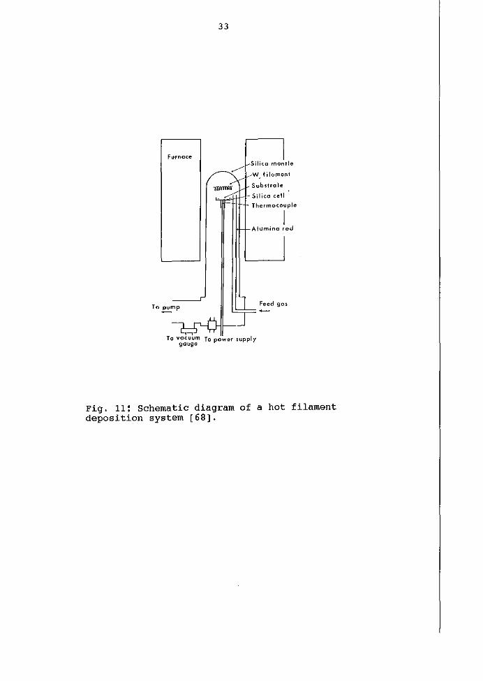
A schematic diagram of the hot filament apparatus is shown
in Fig. 11 [68]. A tungsten filament which can be heated up to
2000 0e is placed in front of, or near the substrate. Gases can
be introduced between the substrate and the filament. Prior to
the deposition, the whole system, which is placed in a quartz
tube, is evacuated to 10-6 mbar with an oil diffusion pump.
The values of the experimental parameters are listed in the
Table 6 [16].
Table 6
Experimental parameters
Total gas pressure
Gas flow rate
eH4 concentration
Substrate temperature
Filament temperature
Substrate potential
Reaction time
30 mbar
0.9-1 l/h
1-12%
S80-880oe
2l00·e
200 V
3 h
Either Si (100) wafers or molybdenum films deposited on
stainless steel are used as substrates. The substrate
temperature is measured with a thermocouple placed inside (when
possible) or close to the substrate. The filament temperature is
controlled by measuring the filament resistance.
Table 7 contains data relative to preparation and
properties of diamond coatings.
36
Certain authors [68,45] used, in addition to the hot
filament, an external furnace to heat the substrate.
In some experiments [16,100] a positive potential of the
substrate holder was applied in order to accelerate electrons,
thus effecting an electron bombardment of the substrate.
In all cases low concentrations (0.5-12%, but typically
a few percent) of hydrocarbon gas (CH4' acetone, other organic
compounds) were used.
A wide range of pressure (0.7-1050 mbar) was used,
although in all the cases relatively narrow ranges were
apparently preferred, mostly at low pressure [16,68,45,100],
except in [92] where 1000 mbar pressure was used.
In a study concerning a more complete utilization of Raman
spectra for characterization of diamond films prepared by the
hot filament method [19], it has been shown that density of
defects in the diamond phase increases as pressure is increased
(the pressure range studied was from 6.5 to 130 mbar).
The filament temperature (Tf) and the filament-substrate
distance were found to be critical: no deposit was formed under
Tf=1730°C and under 1 ern distance [16]. However, higher Tf
(2000-2150 0C) combined with higher CH4 concentration (3%) led
to formation of graphitic carbon [68].
The hydrocarbon concentration in hydrogen was found to be
important: to obtain the diamond phase, the CH4 concentration
had to be not higher than 1% [16,68]. Similar concentrations
were used by other researchers [92,100], but considerably wider
range (0.5-10%) was reported to be suitable if some organic
compounds containing oxygen or nitrogen in addition to carbon
and hydrogen were used [45]. In this particular case a wide
range of pressure (1-1050 mbar) could be used. Because of the
wide ranges of parameters and high deposition rate (8-10 ~m/h),
the authors consider their method as promising for scaling-up.
In all the cases RHEED and SEM were used for
characterization of coatings; Raman spectroscopy was used in all
the cases except in [100]; other methods used were determination
of density [45], electrical characteristics [92], microhardness
[45,100] and boron-dopant concentration [92].
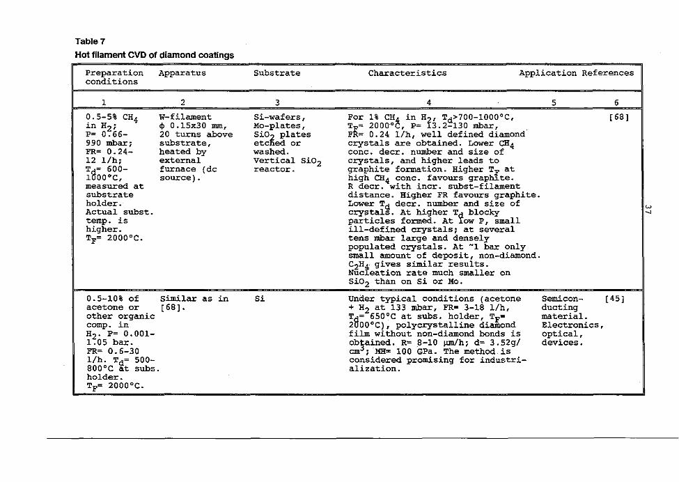
Table 7
Hot filament CVD of diamond coatings
W-.J
Preparation Apparatus Substrate Characteristics Application Referencesconditions
1 2 3 4 5 5
0.5-5% CH4 W-filament 5i-wafers, Por 1% CH~ in H~, Td>700-10000C, [58]in H2; cj> 0.15x30 nun, Mo-plates, T = 2000.0 ,P= 3.2-130 robar,P= 0.55- 20 turns above SiOji plates pK= 0.24 l/h, well defined diamond990 mbar; substrate, etc ed or crystals are obtained. Lower CH4PR= 0.24- heated by washed. conc. deer. number and size of12 l/h; external Vertical 5i02 crystals, and higher leads toTf 500- furnace (de reactor. graphite formation. Higher Tp at100°C, source) . high CH4 conc. favours graph~te.
measured at R deer. with incr. 5ubst-filamentsubstrate distance. Higher FR favours graphite.holder. Lower Td deer. number and size of cActual subst. crystals. At higher T~ blocky .temp. is particles formed. At ow P, smallhigher. ill-defined crystals; at severalTp= 2000°C. tens robar large and densely
populated crystals. At -1 bar onlysmall amount of deposit, non-diamond.C2Ht gives similar results.Nue eation rate much smaller onSi02 than on Si or Mo.
0.5-10% of Similar as in Si Under typical conditions (acetone Semicon- [45]acetone or [68]. + H2 at 133 robar, PR= 3-18 l/h, ductingother organic Tg= 550°C at subs. holder, Tp= material.compo in 200°C), polycrystalline diamond Electronics,H2. P= 0.001- film without non-diamond bonds is optical,1.05 bar. Ob~ained. R= 8-10 ~h; d= 3.52g/ devices.FR= 0.5-30 em ; MH= 100 GPa. The method isl/h. Td~ 500- considered promising for industri-800°C at subs. alization.holder.Tp= 2000°C.
Table 7 continued
wcc
1 2 3 4 5 6
1-2% CH4 in Similar as Sintered Nucleation and growth of diamond [100 JH2; in [116), but SiC plates; film with lattice constant a= 0.3561p= 40 mbar. Me as subst. Si, Mo, we, nm is more rapid than without appliedFR= 3 l/h. holder at TiC. voltage. R= 3-5 JllIl/h. MH= 90 GPa. OnTd= 850°C at positive Si-substrate both diamond and P-SiCsUbs. holder. voltage. are forme~~ Decomposition of CH4 andTF=.1900°C. H2 is accelerated byelectron-bombard-Vs= 150 V. ment.
1-12% CH4 in W-filament Si(lOO) wafer, For filament-substrate distance less Semicon- [16]H2 o placed in front Mo, deposited than 1 em, and TF<1730°C, no deposit ductorp= 30 mbar; of substrate on steel. is formed. For 1% CH4 in H2, FR= 0.9 (if doped),FR= 0.9- (max 1 em l/h; Td= 830°C; TF= 2100 oC, well- optics1.0 l/h. distance). All faceted di!F0nd crystals are obtainedTd = 580- is in a horiz. with no sp bonds. For 4% H2 and.Td=BOOoe; 730°C, both diamond and graphite are ~
TF= 1700- formed. To obtain continuous film,2100°C; the substrate must be polished withVs = 200 V. diamond paste.
Reactant: sat. W-filament 5i(100) wafer Semiconductive B-doped polycrystal- Electronic [92]solution of placed above polished with line diamond films without non- componentsB203 in substrate. diamond paste. diamond bonds detectable by RamanCH30H mixed are obtained. Max B conc. in thewith acetone, fiLms is = 1000 ppm. Slight shift+ H2, 2% of Raman peak with B onc. is found.reactant; p linearly decr. with B conc. forp= 1 bar, = 3 orders of magnitude.FR= 3 l/h,Td= 850°C,TF= 2240°C.
Designations: FR = flow rate; MH = microhardness; R = deposition rate; Td = deposition
temperature; TF = filament temperature; Vs = substrate voltage.
Abbreviations: compo =
sat. =
compound; conc. =
saturated; subs.,
concentration; deer. = decrease; max. = maxLmum;
subst. = substrate; temp. = temperature.
39
Well-defined diamond coatings, consisting of micro
crystals, were reported in all cases, with little or no sp2
bonds present, at least in a certain (chosen) range of working
conditions.
In order to increase nucleation rate, the substrate was
polished with diamond paste [16,68]. A positive voltage applied
to the substrate holder was found to increase the deposition
rate and decomposition of CH4 and H2 [100].Influence of deposition conditions on the diamond
formation was investigated in [16,68]. Rather similar optimum
conditions were found in both cases: 1% CH4 in H2'
Td=700-1000oC, Tf=2000°C, P=13.2-130 robar, FR=0.24-0.9 I/h.
Higher CH4 concentration and 20 times higher FR resulted in
graphite formation [68]. An increase in pressure to 1 bar led
to a small amount of deposit in which no diamond was found [68].
An increase in Tf led to graphite, if CH4 concentration was
also increased, while Td affected mainly the morphology of the
diamond crystals in the coating [68].
The B doping of the diamond coatings was studied in view
of their utilization as semiconductors [92]. Well defined
diamond coatings wLth different B concentrations up to 1000 ppm
were produced. Electrical resistivity of the coatings decreased
linearly with B concentration. A rather wide interval of the
activation energy obtained from a plot of current vs. liT (0.12
0.20 eV in agreement with 0.17-0.18 eV found by others) is
expected to be reduced in a single crystal film.
The substrate nature was found to affect nucleation rate,
in agreement with the results found for the diamond coatings
prepared by other plasma deposition methods (see e. g. microwave
plasma CVD 3.2.3.).
The reactions taking place in the hot filament method are
not fully understood. It is generally thought on the basis of
thermodynamical estimations that CH4 is decomposed through two
decomposition reactions. one is the direct thermal decomposition
near hot filament (CH4 = CH3 + H) and the other is the
abstraction reaction with atomic hydrogen, generated by H2decomposition on the hot filament (CH4 + H = CH3 + H2) [1].
40
However, by thermal decomposition of CH4 at high
temperatures (>1600°C) a quantity of acetylene is produced
which, in turn, leads to deposition of graphitic carbon.
In order to suppress production of acetylene, a modified
hot filament apparatus has been designed [1] in which an upward
stream of hydrogen prevents CH4 from coming to the hot filament,
other working conditions being similar to those in the already
described procedures. The diamond films thus obtained contain
less amorphous ( Sp2) carbon and their crystallinity is better.
The authors express opinion that separation of atomic hydrogen
production from CH4 decomposition may permit a better control
of process parameters in the diamond synthesis.
Thus the hot-filament technique was found to be suitable
for producing polycrystalline, virtually "pure" diamond coatings
(without sp2 bonds) having the structure and properties close to
those of natural diamonds. In particular, microhardness values
are within the interval obtained for the natural diamond. Less
strict requirements regarding conditions of deposition and high
deposition rates attained make the method attractive from the
point of view of its industrialization.
A method combining hot filament, elect~on beam and plasma
CVD has been developed to grow diamond films from gas mixtures
containing CH4' H2 and Ar [60]. The apparatus and procedure aims
at creating favourable conditions for high nucleation first, and
then for a high rate of growth.
The conclusions are not much different from those obtained
by other researchers. Diamond can be deposited at 640-800 oC,
at 6.5-40 mbar with 0.24-2.0 vol% CH4 in H2, but temperature and
pressure should vary to obtain optimum conditions.
The nucleation density is enhanced by scratching the
substrate surface with diamond powder, but nucleation is also
initiated without it. With respect to sapphire, silicon takes
much longer time to form nuclei. Diamond layer grown on Si has
a good adhesion, but transition layer is necessary on sapphire
because of big difference in thermal expansion coefficients.
The deposition rate obtained is 1 ~m/h.

41
3.2 Plasma chemical vapour deposition
3.2.1 Direct current plasma CVD of diamond and diamondlike
coatings
The most simple method of activation of a gas phase is to
produce a glow discharge using a high dc voltage. This may be
the reason why the first successful experiments on plasma CVD
of DLC were made with such a discharge [105].
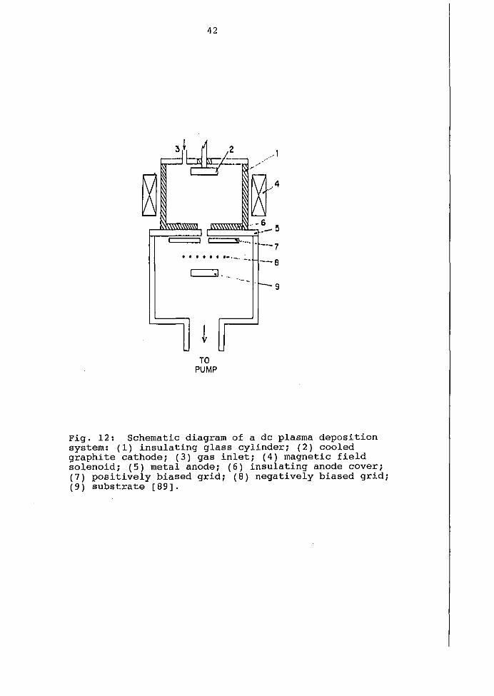
A schematic diagram of the experimental set-up, as used in
[89], is shown in Fig. 12. A glass cylinder 7.5 cm in diameter
and 30.5 cm long contained a dc glow discharge. The cathode was
a water-cooled graphite rod. The gas entered through a hole near
to the cathode.
Typical discharge conditions were 600 V and 0.1 A.
A coaxial magnetic field produced by the solenoid helped to
stabilize the discharge, which was operating in the abnormal
glow discharge region at a pressure of about 65 ~bar.
The plasma density was increased near the anode by
an insulating disc. The plasma was extracted through a hole
2.0-2.5 mm in diameter in the anode and passed through the
positively biased grid with an aperture of about 6.0 mm
diameter. A second grid which was negatively'biased in the
range 100-2000 V accelerated the ions towards the substrate
while repelling the electrons.
This arrangement resulted in an ion beam of fairly uniform
energy and permitted the investigation of the effect of ion
energy on film properties. Since the diamondlike coating is an
insulator, a floating potential is established at the surface of
the substrate. It could be varied by changing the voltage of the
grid. No thermionic filament was used. The pressure in the
deposition chamber was in the 10-4 mbar range.
The gas consisted of roughly equal amounts of C2H2 and
CO2, sometimes with some addition of argon. The gas pressure
increased by about 50% when the discharge was started.
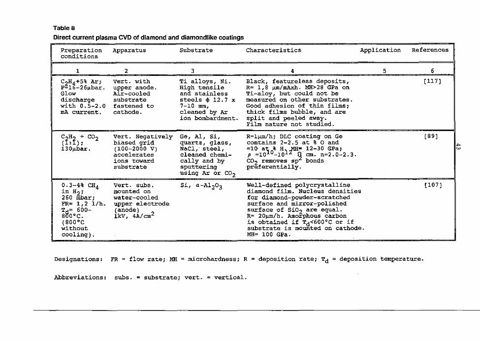
Table 8 illustrates the experiments and results obtained
with this type of discharge.
..... . ..'--..:..-
42
,....... ~
--7
--B
TOPUMP
Fig. 12: Schematic diagram of a dc plasma depositionsystem: (1) insulating glass cylinder; (2) cooledgraphite cathode; (3) gas inlet; (4) magnetic fieldsolenoid; (5) metal anode; (6) insulating anode cover;(7) positively biased grid; (8) negatively biased grid;(9) substrate [89].
TableS
Direct current plasma CVD of diamond and diamondlike coatings
..w
Preparation Apparatus Substrate Characteristics Application Referencesconditions
1 2 3 4 5 6
C2H~+5% Ar; vert. with Ti alloys, Ni. Black, ~eatureless deposits, [117]P=l -26Il-bar. upper anode. High tensile R= 1,8 um/mnxh , MH>28 GPa onGlow Air-cooled and stainless Ti-aloy, but could not bedischarge substrate steels <I> 12.7 x measured on other substrates.witb 0.5-2.0 fastened to 7-10 IDm, Good adhesion of thin films;rnA current. cathode. cleaned by Ar thick films bubble, and are
ion bombardment. split and peeled away.FiLm nature not studied.
Ct~ + CO2 Vert. Negatively Ge, AI, 5i, R=l~/h; DLe coating on Ge [89]( : ); biased grid quartz, glass, contains 2-2.5 at %0 and
"l30ll-bar. (100-2000 V) NaCl, steel, =10 a\O% H).fB:= 12-30 GPa; ,accelerates cleaned chemi- p =10 -10 q em. n=2.0-2.3.ions toward cally and by CO2 removes sp bondssubstrate sputtering preferentially.
using Ar or CO2
0.3-4% CH4 Vert. subs. 8i, a-A1 203 Well-defined polycrystalline [107Jin H2; mounted on diamond film. Nucleus densities260 mbar; water-cooled for diamond-powder-scratchedFR= 1,2 l/h. upper electrode surface and mirror-polishedTf 600- (anode) surface of 8i02 are-equal.80°C. lkV, 4A/em2 R= 20lJlll!h. Amorphous carbon(800°C is obtained if Td<600°C or ifwithout substrate is mounted on cathode.cooling) . MIl= 100 GPa.
Designations: FR = flow rate; MH = microhardness; R deposition ratei,Td deposition temperature.
Abbreviations: subs. substrate; vert. vertical.
44
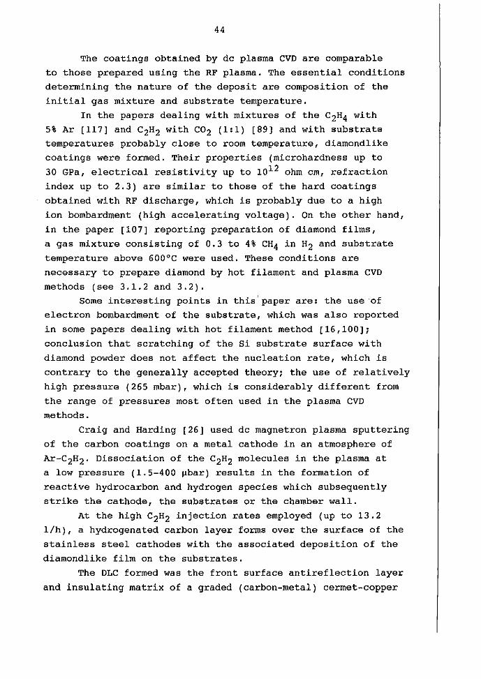
The coatings obtained by dc plasma CVD are comparable
to those prepared using the RF plasma. The essential conditions
determining the nature of the deposit are composition of the
initial gas mixture and substrate temperature.
In the papers dealing with mixtures of the C2H4 with
5% Ar [117] and C2H2 with C02 (1'1) [89] and with substratetemperatures probably close to room temperature, diamondlike
coatings were formed. Their properties (microhardness up to
30 GPa, electrical resistivity up to 1012 ohm cm, refraction
index up to 2.3) are similar to those of the hard coatings
obtained with RF discharge, which is probably due to a high
ion bombardment (high accelerating voltage). On the other hand,
in the paper [107] reporting preparation of diamond films,
a gas mixture consisting of 0.3 to 4% CH4 in H2 and substrate
temperature above 600°C were used. These conditions are
necessary to prepare diamond by hot filament and plasma CVD
methods (see 3.1.2 and 3.2).Some interesting points in this'paper are: the use ·of
electron bombardment of the substrate, which was also reported
in some papers dealing with hot filament method [16,100];
conclusion that scratching of the 6i substrate surface with
diamond powder does not affect the nucleation rate, which is
contrary to the generally accepted theory; the use of relatively
high pressure (265 mbar) , which is considerably different from
the range of pressures most often used in the plasma CVD
methods.
Craig and Harding [26] used dc magnetron plasma sputtering
of the carbon coatings on a metal cathode in an atmosphere of
Ar-C 2H2. Dissociation of the C2H2 molecules in the plasma at
a low pressure (1.5-400 ~bar) results in the formation of
reactive hydrocarbon and hydrogen species which subsequently
strike the cathode, the substrates or the chamber wall.
At the high C2H2 injection rates employed (up to 13.2
l/h), a hydrogenated carbon layer forms over the surface of the
stainless steel cathodes with the associated deposition of the
diamondlike film on the substrates.
The DLC formed was the front surface antireflection layer
and insulating matrix of a graded (carbon-metal) cermet-copper
45
solar selective surface operating as a solar absorber IR
reflector tandem fur all-glass evacuated tubular collectors.
The deposited films contain a large amount of hydrogen
(up to 42.6 at%) and up to 6.7 at% of oxygen and have a low
density (0.98-1:6 g/cm3 ) . Their refraction index (for film
thickness greater than 80 nm) is 1.8-1.9 in the wavelength range
0.3-2.5 ~m, and electrical resistivity is above 10 7 ohm cm.
The optical band gap (Eg) increases with H/C ratio
(from 1.1 eV at H/c=0.2 to 2.0 eV at H/C=0.8).
The authors conclude that the basic OLC structure is
a random network of C-atoms in tetrahedral coordination with
nearest neighbours.
The deviations of bond lengths and angles from diamond
lattice values are minor, althougth the distribution of second
and further neighbours is highly disordered. The tetrahedral
carbon network is modified by C=C bonds and the inclusion of
hydrogen of the order H/C=0.5 in monohydride and dihydride
bonding configurations. After heat-treatment at 500°C, during
which large quantities of H2 and CO evolve, the film becomes
thermally stable which is believed to result from residual
Hand 0 atoms occupying fixed sites in the OLC network
characterized by an absence of near-neighbour H atoms.
Thus, it can be concluded that the dc plasma cva is
a method which can be successfully applied for both OLC and
OC preparation. The fact that this method has been relatively
little used is associated with difficulties involved in
neutralization of the surface charge and in ensuring uniform
thickness of the layers over a surface area greater than
a couple of cm2.
3.2.2 Radio Frequency (RF) Plasma chemical vapour deposition
RF plasma deposition of diamondlike coatings
By far the most widespread deposition process employed to
deposit diamondlike carbon films makes use of a low pressure RF
46
glow discharge in hydrocarbons or their mixtures with inert
gases. After the pioneering work of Holland and Ojha [46], this
method rapidly became popular allover the world.
There are several reasons why the RF discharge has been so
widely investigated. An important advantage is that standard,
commercially available equipment intended for preparation of
thin films by cathode sputtering can be used. Another advantage
comes from the fact that by using the RF plasma one of the
greatest problems involved in deposition of dielectric films on
various substrates, including the non-conducting ones, can be
successfully solved. The RF excited plasma exposes the substrate
to positive ions and to electrons alternately and thus prevents
any net charge accumulation on non-conducting deposits.
Reactor system
A schematic diagram of the deposition set-up as used in
[21] is given in Fig. 13. The reaction vessel 35 cm in diameter
and 22.5 cm in height is made of stainless steel. The electrodes
are water-cooled stainless steel discs 12.7 ern in diameter (area
about 127 cm2). The interelectrode spacing is 6.5 cm.
The discharge is sustained in CH4 or C6H6 or their mixture
(5 vol % and 7.6 vol % respectively) with helium by means of
a 13.56 MHz RF power source. The power is coupled to the excited
electrode via an L-type capacitive matching network for the high
frequency discharge (13.56 MHz), the other electrode being
grounded. All the substrates (glass or silicon) are set on the
powered electrode. The discharge pressure is measured with
a capacitance manometer which drives a trottling valve to keep
a constant pressure during all deposition cycle which may last
for several hours. The entire system is pumped down with
a mechanical pump which gives an ultimate vacuum of 1.3 robar.
The high purity gases are used without further purification.
The benzene vapor is obtained by the vaporization at room
temperature of spectroscopically pure liquid benzene.
The general deposition conditions are summarized in the
Table 9 [21].
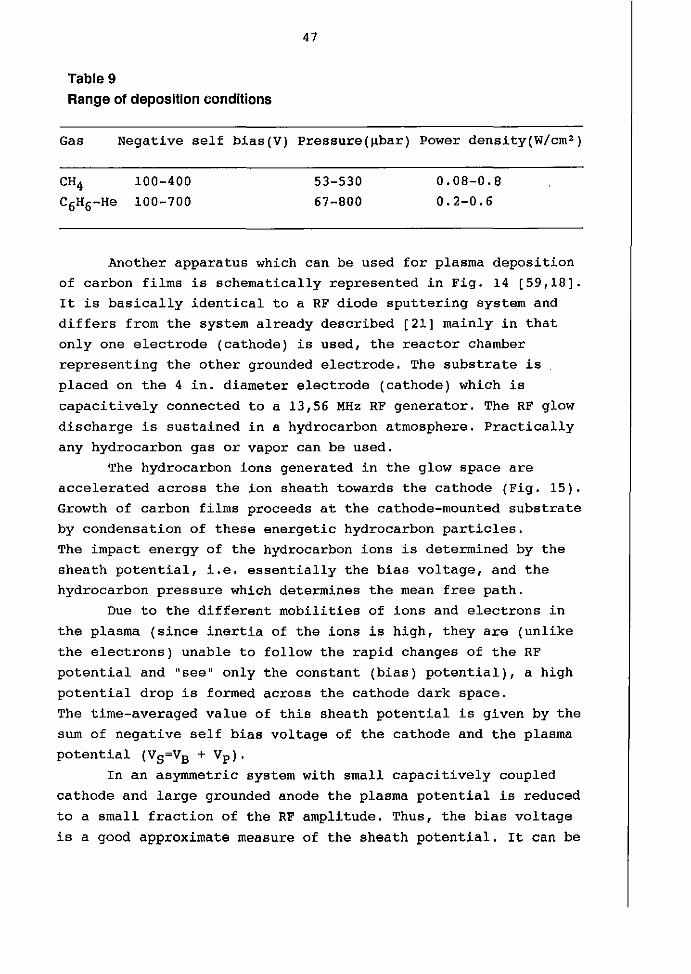
47
Table 9
Range of deposition conditions
Gas Negative self bias(V) Pressure(~bar) Power density(w/cm')
100-400
100-700
53-530
67-800
0.08-0.8
0.2-0.6
Another apparatus which can be used for plasma deposition
of carbon films is schematically represented in Fig. 14 [59,18].
It is basically identical to a RF diode sputtering system and
differs from the system already described [21] mainly in that
only one electrode (cathode) is used, the reactor chamber
representing the other grounded electrode. The substrate is
placed on the 4 in. diameter electrode (cathode) which is
capacitively connected to a 13,56 MHz RF generator. The RF glow
discharge is sustained in a hydrocarbon atmosphere. Practically
any hydrocarbon gas or vapor can be used.
The hydrocarbon ions generated in the glow space are
accelerated across the ion sheath towards the cathode (Fig. 15).
Growth of carbon films proceeds at the cathode-mounted substrate
by condensation of these energetic hydrocarbon particles.
The impact energy of the hydrocarbon ions is determined by the
sheath potential, i.e. essentially the bias voltage, and the
hydrocarbon pressure which determines the mean free path.
Due to the different mobilities of ions and electrons in
the plasma (since inertia of the ions is high, they are (unlike
the electrons) unable to follow the rapid changes of the RF
potential and "see" only the constant (bias) potential), a high
potential drop is formed across the cathode dark space.
The time-averaged value of this sheath potential is given by the
sum of negative self bias voltage of the cathode and the plasma
potential (VS=VB + Vp).In an asymmetric system with small capacitively coupled
cathode and large grounded anode the plasma potential is reduced
to a small fraction of the RF amplitude. Thus, the bias voltage
is a good approximate measure of the sheath potential. It can be
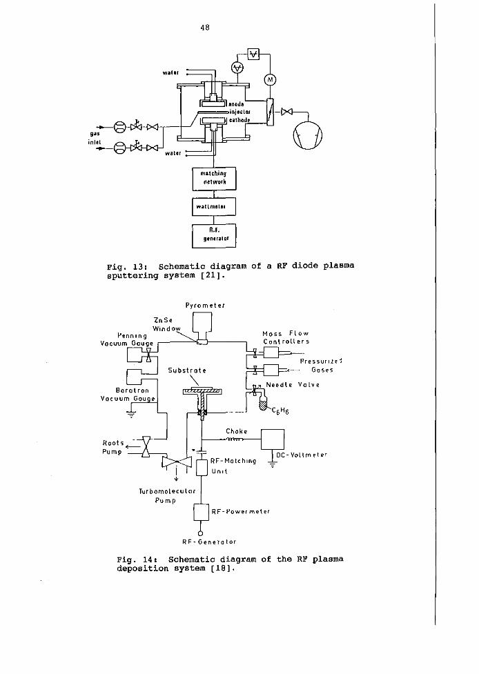
48
wain
g.~,~-W ~inlet ~==;;UILIT==9
water :::==:)J
Fig. 13, Schematic diagram of a RF diode plasmasputtering system [21].
Pyrometer
Zn SeWindow
Substrote
-,
Choke
ROot5~
PumpRF-Molchlng
Unit
Turbomolecular
Pump
RF-Powermeter
RF· Ge n er o t cr
Pressurize 1Goses
Vo l v e
Fig. 14: Schematic diagram of the RF plasmadeposition system [18].
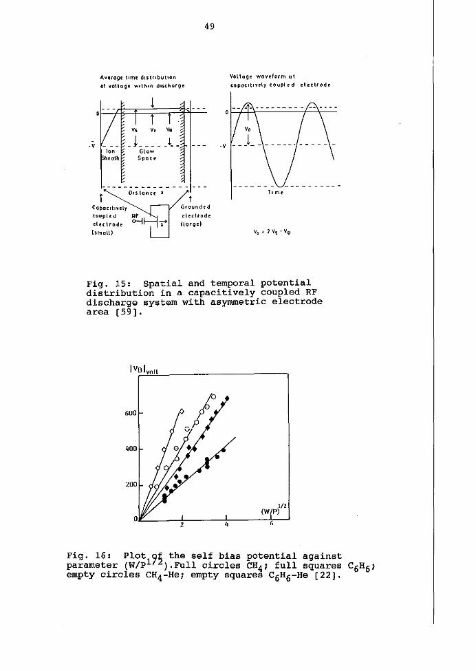
49
Average time distributIon
01 voltage wltI'IIll discharge
VoLioge waveform ot
capocltIVel)' coupt e d electrode
-v
tCapacltlyel)'coupled
et e c tr oce
hmolll
Vs Vp VB
GlowSpa c e
D's lance
Grounded
electrode
IlofgcJ
·v
Fig. 15: Spatial and temporal potentialdistribution in a capacitively coupled RFdischarge system with asymmetric electrodearea [59].
1{2(w/P)
6
Fig. 16: Plotl~~ the self bias potential againstparameter (W/P ).Full circles CH4; full squares C6H6;empty circles CH4-He; empty squares C6H6-He [22].
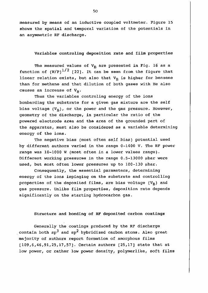
50
measured by means of an inductive coupled voltmeter. Figure 15
shows the spatial and temporal variation of the potentials in
an asymmetric RF discharge.
Variables controling deposition rate and film properties
The measured values of VB are presented in Fig. 16 as a
function of (w/p)I/2 [22]. It can be seen from the figure that
linear relation exists, but also that VB is higher for benzene
than for methane and that dilution of both gases with He also
causes an increase of Va'
Thus the variables controling energy of the ions
bombarding the substrate for a given gas mixture are the self
bias voltage (VB)' or the power and the gas pressure. However,
geometry of the discharge, in particular the ratio of the
powered electrode area and the area of the grounded part of
the apparatus, must also be considered as a variable determining
energy of the ions.
The negative bias (most often self bias) potential used
by different authors varied in the range 0-1400 V. The RF power
range was 10-1000 W (most often in a lower values range).
Different working pressures in the range 0.5-13000 ~bar were
used, but most often lower pressures up to 100-130 ~bar.
Consequently, the essential parameters, determining
energy of the ions impinging on the substrate and controlling
properties of the deposited films, are bias voltage (VB) and
gas pressure. Unlike film properties, deposition rate depends
significantly on the starting hydrocarbon gas.
Structure and bonding of RF deposited carbon coatings
Generally the coatings produced by the RF discharge
contain both sp3 and sp2 hybridized carbon atoms. Also great
majority of authors report formation of amorphous films
[109,6,46,91,25,17,57]. Certain authors [25,17] state that at
low power, or rather low power density, polymerlike, soft films
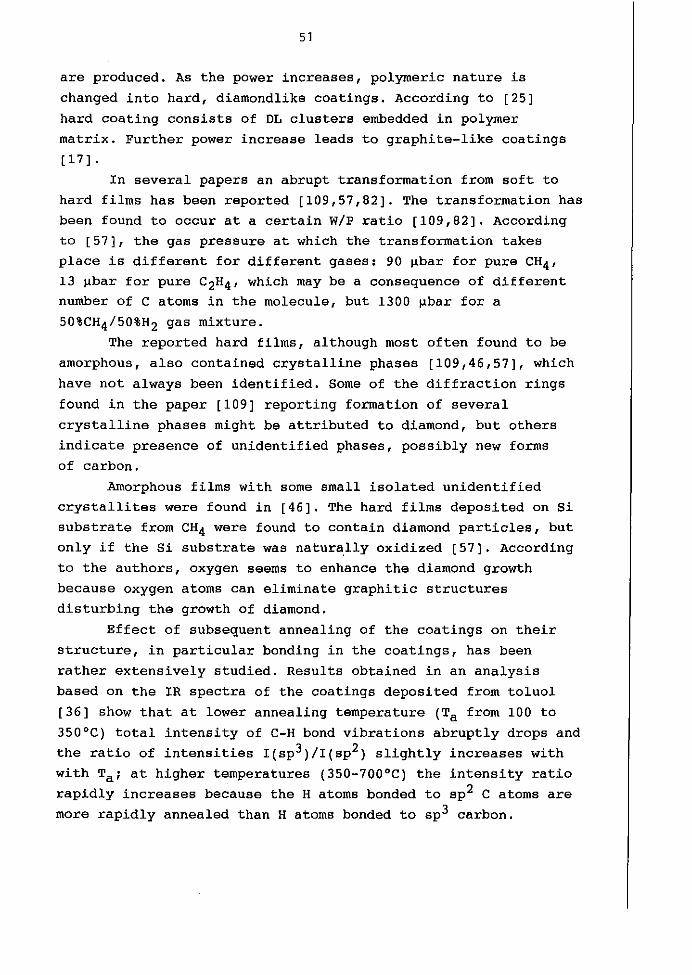
51
are produced. As the power increases, polymeric nature is
changed into hard, diamondlike coatings. According to [25]
hard coating consists of DL clusters embedded in polymer
matrix. Further power increase leads to graphite-like coatings
[17].
In several papers an abrupt transformation from soft to
hard films has been reported [109,57,82]. The transformation has
been found to occur at a certain W/P ratio [109,82]. According
to [57], the gas pressure at which the transformation takes
place is different for different gases: 90 ~bar for pure CH4'
13 ~bar for pure C2H4' which may be a consequence of different
number of C atoms in the molecule, but 1300 ~bar for a
50%CH4/50%H2 gas mixture.
The reported hard films, although most often found to be
amorphous, also contained crystalline phases [109,46,57], which
have not always been identified. Some of the diffraction rings
found in the paper [109] reporting formation of several
crystalline phases might be attributed to diamond, but others
indicate presence of unidentified phases, possibly new forms
of carbon.
Amorphous films with some small isolated unidentified
crystallites were found in [46]. The hard films deposited on Si
substrate from CH4 were found to contain diamond particles, but
only if the Si substrate was natur~lly oxidized [57]. According
to the authors, oxygen seems to enhance the diamond growth
because oxygen atoms can eliminate graphitic structures
disturbing the growth of diamond.
Effect of subsequent annealing of the coatings on their
structure, in particular bonding in the coatings, has been
rather extensively studied. Results obtained in an analysis
based on the IR spectra of the coatings deposited from toluol
[36] show that at lower annealing temperature (Ta from 100 to
350°C) total intensity of C-H bond vibrations abruptly drops and
the ratio of intensities I( Sp3)/I( s p2) slightly increases with
with Tal at higher temperatures (350-700°C) the intensity ratio
rapidly increases because the H atoms bonded to sp2 C atoms are
more rapidly annealed than H atoms bonded to sp3 carbon.
52
In a similar study in which vacuum annealing of hard
DL coatings was performed at different Ta up to 600°C [59],it was found that sp3 sites and olefinic sp2 sites exist.
The composition of the as-deposited films containing 68% sp3
sites, 30% sp2 and 2% sp1 sites is s1igtly changed upon
annealing to 300°C, but above this temperature hydrogen is
evolved and drastic change in the bonding occurs.
The work based on the photoemission spectra of DL films
obtained from toluol [95] confirms the previously mentioned
conclusions [59] in that the sp3 bonding decreases at Ta>350oC.However, the sp3/sp2 ratio was found to reach saturation at
about 500°C. In addition, it is concluded that the sp3 content
increases up to Ta=350oC.An interesting experimental result is that properties
of the hard films deposited from different hydrocarbons under
identical conditions, are independent of the nature of the
starting hydrocarbon [59,6], even although hydrocarbons with·
different types of bonding (such as benzene and methane) are.
used [59]. This is even more surprising knowing that these
hydrocarbons behave differently in the RF discharge (e.g.
different ionic species are formed) [59]. The explanation of:
these experimental observations is that the relatively high
energy of the plasma leads to efficient fragmentation of the'
hydrocarbon gases, so that small fragments, such as C, C2 or
CH may be regarded as the actual precursors for DL film growth
[59].
This is not true, however, when soft, polymerlike films are
considered. Namely, properties of soft films generally depend
on the starting hydrocarbon gas, because under such conditions
larger fragments of the hydrocarbon molecules can be
incorporated into the film [59].
Influence of deposition conditions on coating properties
Deposition rate values were reported in a number of papers
[46,32,33,6,21,31,95]. The values vary in a wide range, from·
0.03 ~m/h [33] to 72 ~m/h [95], but the majority of them are ·of
53
the order of several ~m/h. The deposition rate was found to
increase with RF power, bias voltage and hydrocarbon pressure
[33]. Addition of inert gases (Ar,He) which stabilize plasma by
increasing its conductivity, sharply reduces deposition rate
[120]. For hydrocarbon gases having the same structural form,
deposition rate was found to increase with molecular weight [6].
According to the paper [21], mass deposition rate should
be distinguished from thickness rate, the former increasing
linearly vith p1/2 and the latter increasing quasi-linearly with
the product VBP. This difference is explained by variation in
film density, which was found to increase linearly from 1.3 to
1:6 9/cm3 with the reduced parameter VBP-1/ 2. Since the ion
energy is also proportional to this parameter (18), it follows
that densification of the layers is the result of the ion
bombardment.
In an apparatus employing inductive coupling of the RF
source and thus permitting control of the bias power
iridependently of the RF power, use of an additional magnetic
field produced an increase in deposition rate by a factor 5 to
10, reaching about 45 ~m/h and permitting to obtain reasonable
values even at a low pressure (eg. 2.9 ~m/h at 0.5 ~bar pressure
[31] .
Amorphous carbon films can contain large amounts of
hydrogen, exceeding 50 at% [59]. A number of methods were used
to determine hydrogen content, but those most widely used are
IR absorption and nuclear reaction analysis. The former methods,
aithough detecting only chemically bonded and not chemisorbed
or trapped hydrogen, can show not only (relative) hydrogen
concentrations, but also details of chemical bonding. Hydrogen
not chemically bonded to carbon, which may amount to more than
30%, may be trapped by ion implantation and burial from bond
breakage during growth, and causes a compressive stress which
can result in disintegration of thick films (>1 ~m) [47].
A number of researchers studied correlations between
hydrogen, content and/or its bonding and other coating properties
[47,25,120,59,57,90,36,31]. It is logical to expect such
correlations, because hydrogen as a bond-terminating atom,
piays central role in determining the coating properties [59].
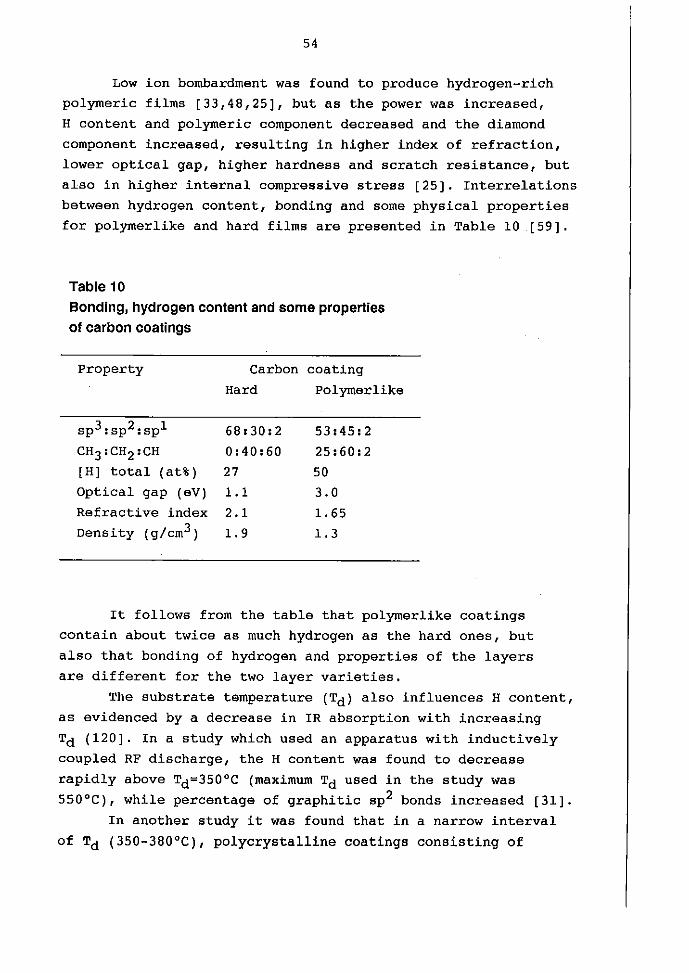
54
Low ion bombardment was found to produce hydrogen-rich
polymeric films [33,48,25], but as the power was increased,
H content and polymeric component decreased and the diamond
component increased, resulting in higher index of refraction,
lower optical gap, higher hardness and scratch resistance, but
also in higher internal compressive stress [25]. Interrelations
between hydrogen content, bonding and some physical properties
for polymerlike and hard films are presented in Table 10 [59].
Table 10Bonding, hydrogen content andsome propertiesof carbon coatings
Property
sp3:sp2:spl
CH3:CH2:CH[H] total (at%)
Optical gap (eV)
Refractive index
Density (g/cm 3 )
Carbon
Hard
68.30:2
0:40:60
27
1.1
2.1
1.9
coating
Polymerlike
53:45:2
25:60:2
50
3.0
1. 65
1.3
It follows from the table that po1ymerlike coatings
contain about twice as much hydrogen as the hard ones, but
also that bonding of hydrogen and properties of the layers
are different for the two layer varieties.
The substrate temperature (TdJ also influences H content,
as evidenced by a decrease in IR absorption with increasing
Td (120]. In a study which used an apparatus with inductively
coupled RF discharge, the H content was found to decrease
rapidly above Td=350°C (maximum Td used in the study was
550°C), while percentage of graphitic sp2 bonds increased [31].
In another study it was found that in a narrow interval
of Td (350_380°C), polycrysta1line coatings consisting of
55
carbine and graphite are obtained, while the coatings prepared
at 620-800 oC consist of carbine, defected diamond and graphitic
carbon [125].
Hydrogen content and optical gap were found to be
inversely related to microhardness [90], in agreement with the
mentioned results of other authors.
Generally, increased hardness of coatings is followed by
an increase in density, electrical resistivity and index of
refraction, as well as a decrease in H content and optical gap
values. Fig. 17 [59], showing dependence of film properties on
the self-bias voltage, illustrates behaviour of all these
properties except for electrical resistivity.
According to different authors (Table 11) the soft
(polymer1ike) films with hardness 4 on the Mohs' scale [87] have
low density (1.3 g/cm3) [59], low refraction index (1.60-1.65)
[59,34], and large optical gap (3.0 ev) [59]. Hard films with
hardness of 30-46 GPa [120,6,57] or 7-8 on the Mohs'scale
[17,87] are characterized by high density (1.9-2.12 g/cm3)
[59,6,17,57], high electrical resistivity (10 9 - 10 13 ohm em)
[48,17,57,87,6,31], high index of refraction (2.0-2.2)
[109,120,59,34], optical gap between 1.1 and 0.8 eV [59] and
high breakdown strength (>10 6 ev) [39,87].
Kobayashi et al. [58] have measured sputtering rates of
various diamondlike and diamond films prepared by RF plasma
deposition and by hot filament methods, respectively. Behaviour
of sputtering rate of the DLF is similar to that of H content
of the films. Both increase with increasing CH4 pressure during
the deposition and decrease with increasing power. On the other
hand, sputtering rate depends on (decreases with) the film
hardness, the ratio of sputtering rates of the films being
directly related to the ratio of their hardness. That this
dependence is extended to diamond films follows from a
comparison of sputtering rates of the DL films and the diamond
ones: the former are sputtered 3 times more rapidly than the
latter, which can be compared to their hardness (35 and
70-100 GPa, respectively).
Since the early successful attempts to produce DLC it has
been observed that the layers exhibit compressive stress and,
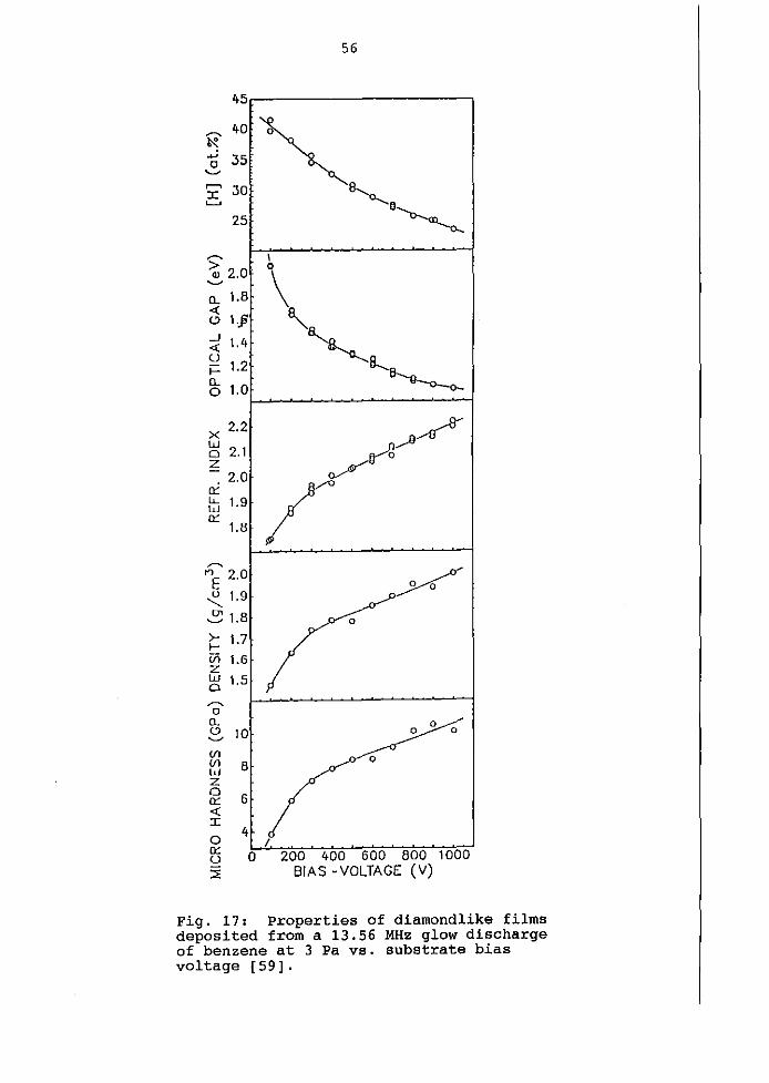
56
45
~40
~~..J 350~
~ 30I
"'---~~
25
~ \> 0
Q) 2.0
\~
CL 1.8<{ 1.p
'~'-'-' 1.4-cu;:: 1.2
~-o-c...CL1.00
x 2.2 ..--0/w0 2.1 ~z .»:2.00:: Iu, 1.9w0::
1.8
~
"'E 2.0 0 0
~ 1.9~ 1.8 0
>- 1.7>--in 1.6Zw 1.50~
00.. 0'-' 10 0 0~
(Il0(Il 8w
z0 60::<{I
04
I0:: 0 200 400 600 800 1000u::E BIAS -VOLTAGE (V)
Fig. 17: Properties of diamondlike filmsdeposited from a 13.56 MHz glow dischargeof benzene at 3 Pa vs. substrate biasvoltage [59].
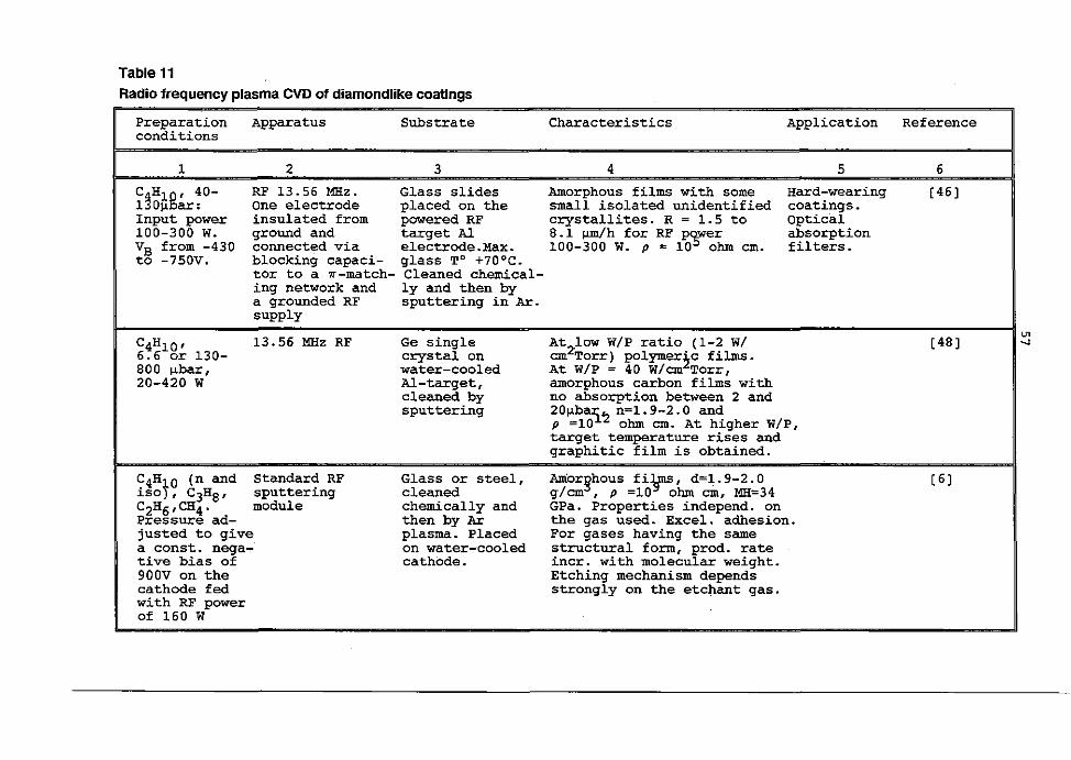
Table 11
Radio frequency plasma CVD of diamondlike coatings
Preparation Apparatus Substrate Characteristics Application Referenceconditions
1 2 3 4 5 6
CjH1g,40- RF 13.56 MHz. Glass slides Amorphous films with some Hard-wearing [46]
1 O~ ar: One electrode placed on the small isolated unidentified coatings.Input power insulated from powered RF crystallites. R=1.5to Optical100-300 w. ground and target Al 8.1 ~/h for RF p~wer absorptionVB from -430 connected via electrode.Max. 100-300 w. p = 10 ohm em. filters.to -750V. blocking capaci- glass TO +70°C.
tor to a ~-match- Cleaned chemical-ing network and 1y and then bya grounded RF sputtering in Ar.supply
C4H1 0, 13.56 MHz RF Ge single At2~ow w/p ratio (1-2 wi [48]6.6 or 130- crystal on em Torr) polymer~c films.800 IJ.bar, water-cooled At w/p = 40 w/cm Torr,20-420 W Al-target, amorphous carbon films with
cleaned by no absorption between 2 andsputtering 20~ba~ n=1.9-2.0 and
p =10 ~ ohm em. At higher w/p,target temperature rises andgraphitic film is obtained.
C4HtO(n and Standard RF Glass or steel, Amor~hous fi~, d=1.9-2.0 [ 6]iso , C3HS 1 sputtering cleaned g/cm , p =10 ohm em, MH=34C2H6,CH4· module chemically and GPa. Properties independ. onPressure ad- then by Ar the gas used. Excel. adhesion.justed to give plasma. Placed For gases having the samea canst. nega- on water-cooled structural form, prod. ratetive bias of cathode. incr. with molecular weight.900V on the Etching mechanism dependscathode fed strongly on the etc~ant gas.with RF powerof 160 W
'"-.J
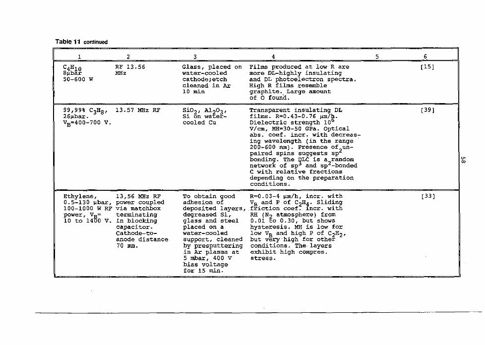
Table 11 continued
1 2 3 4 5 6
C4H1 0 RF 13.56 Glass, placed on Films produced at low R are [15]S~bar MHz water-cooled more DL-highly insulating50-600 W cathode; etch and DL photoelectron spectra.
cleaned in Ax High R films resemble10 min graphiteo_ Large amount
of ° found.
99,99% C3HS' 13.57 MHz RF Si02, Al 203, Transparent insulating DL [39]26~bar. 5i on water- films. R=0.43-0.76 ~/g.
VB=400-700 V. cooled Cu Dielectric strength 10V/cm, MH=30-50 GPa. Opticalabs. coef . incr. with decreas-ing wavelength (in the range200-600 nrn). Presence of un-paired spins suggests sp2bonding. The ~LC is a
2randomnetwork of sp and sp -bondedC with relative fractionsdepending on the preparationconditions.
Ethylene, 13,56 MHz RF To obtain good R~0.03-4 ~/h, incr. with [33]0.5-130 ~bar, power coupled adhesion of VB and P of C2H4. Sliding100-1000 W RF via matchbox deposited layers, .friction caef. ~ncr. withpower, Vij= terminating degreased Si, RH (N2 atmosphere) from10 to 14 0 V. in blocking glass and steel 0.01 to 0.30, but shows
capacitor. placed on a hysteresis. MH is low forCathode-to- water-cooled low VB and high P of C2H2'anode distance support, cleaned but very·high for other70 mm. by presputtering conditions. The layers
in Ar plasma at exhibit high compres.5 mbar, 400 V stress.bias voltagefor 15 min.
'J'ex>
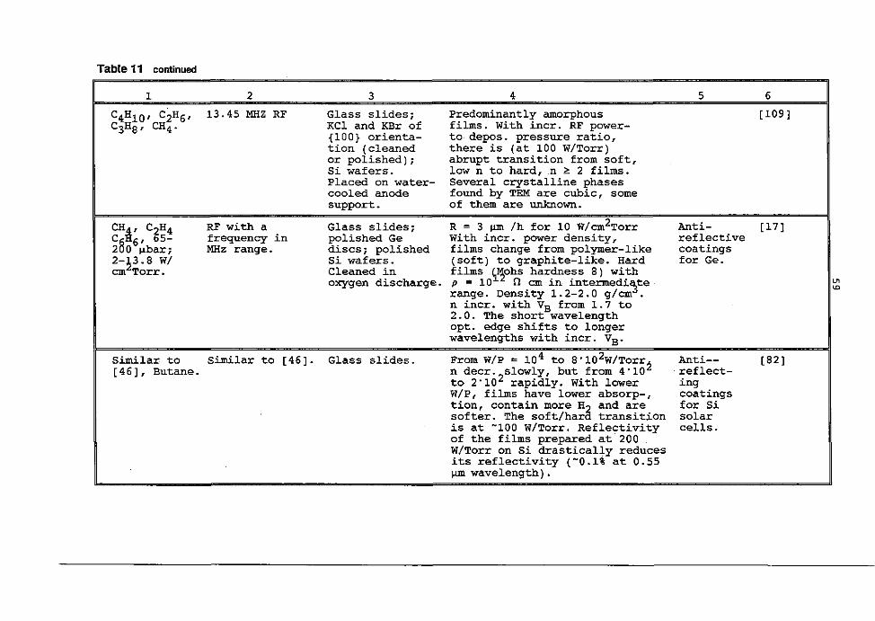
Table 11 continued
encc
1 2 3 4 5 6
C4Hl O' C2H6, 13.45 MHZ RF Glass slides; Predominantly amorphous [109]C3HS' CH4· KCl and KBr of films. With incr. RF power-
{laO} orienta- to depos. pressure ratio,tion (cleaned there is (at 100 W/Torr)or polished) i abrupt transition from soft,8i wafers. low n to hard, :n ~ 2 films.Placed on water- Several crystalline phasescooled anode found by TEM are cubic, somesupport. of them are unknown.
CH~, Ct4 RF with a Glass slides; R = 3 ~ Ih for 10 W/em2Torr Anti- [17]Cs 6' 5- frequency in polished Ge With incr. power density, reflective2 0 IJ.bar; MHz range. discs; polished films change from polymer-like coatings2-p.S wi 8i wafers. (soft) to graphite-like. Hard for Ge.em Torr. Cleaned in films ~~ohs hardness 8) with
oxygen discharge. p = 10 n em in intermedi~te,,
range. Density 1.2-2.0 g/cm .n incr. with VB from 1.7 to2.0. The short wavelengthopt. edge shifts to longerwavelengths with incr. VB'
Similar. to Similar to [46]. Glass slides. From W/P = 10 4 to S·102w/Torr~ Anti-- [S2][46], Butane. n decr.
2slowly,but from 4·10 reflect-
to 2'10 rapidly. With lower ingW/p, films have lower absorp-, coatingstion, contain more Haand are for Sisofter. The soft/har transition solaris at -100 W/Torr. Reflectivity cells.of the films prepared at 200W/Torr on Sidrastically reducesits reflectivity (-0.1% at 0.55~ wavelength).
Table 11 continued
"'o
1 2 3 4 5 6
CH4 plasma 13.56 MHz RF Single crystal Transparent amorphous films with Optical [l1B 1wafers of Si, less than 20% of tetrahedral C-C coatingsGaAs and InP; bonds. H ~ontent·~ 40%. Er=2.7ev. especial-
No change in properties b ly forannealing to 500-600°C, but ), >500nm.graphitization at higher T.H content drops at 900°C to5%, but surface H remains.
CH~, Ct~' RF 13 MHz. Glass, quartz, OLe film surfaces contain onl¥ C, [B7]C3 g' 3 6; Symmetrical single crystal with occasional traces of O. Egde ias 0 diode-reactor, 5i-wafers, depends strongly on Wand biasto -400 V; connected to RF KBri Au on voltage. Eg values up to 2.7 eV25-200 W via impedance- quartz (from CH4). MH up to 7 Mohs. E
matching and H content are in~~sely gnetwork. related to MH. P >10 ,n ern; ,
dc breakdown strength >B.0·10 6V/cm. IR vibr,tional frequenciestypical of sp bonding, and(weak) C-H absorption found.
CH4 (5vol%) 13.56 MHz RF. Glass or Si, R up to 2.9 ~/h. V¥ ~ncr. [21]or C6H6 Reaction vessel pla~ed.on the linearly with (W/P) / . VB is(7.6 vol %) 35 cm dia., powered higher for C6H6 and for He-in He. For 22.5 em high. electrode. diluted gases. Mass depos 2ateCH4: 53-530 12.7 cm dia. increases linearly with pi/ anduber , O.O~- water-cooled thickness rate (R) incr. with VBP.10.B W/em ; stainless steel Little effect of W. Incr. in RFfor CaHf electrodes, power density leads to lower depos.80-27 J.1 ar, spaced 6.5 cm. thickness. Film is densified by0.2-0.B W/cm. ion bombardment.
Table 11 continued
'"
1 2 3 4 5 6
CH4, CHa(5%)
~s foregoing 8i; glass High ion bombardment (IB) 1ea~s Protective [25]-He, C6 6 to lesser H-content and to sp~; coatings(7.6%) low IB ~roduces C-H
2bondsin sp
-ne , ; CH3, sp CH2 and sp CH2, the films70-700 ~bar are of Polymeric nature. n=1.88-2 ..56Td <60°C in pure CHa, iner. with VB E0-100 W between O. and 1. 8 eV. polymgric0-0.79 w/cm2 component deer. with W from 63 toVB = 0-700 V. 53% and diamond iner. from 23 to
33%. Graphite-like component is9-13%. High hardness and scratchresistance. High internal compres-sive stresses, ioer. with deer.H content.
CH +H • RF 13.56 MHz Two 0.2 mm dia Soft and hard films were obtained [57] ,
C§a4+~a; W probes. at higher and lower gas pressure,( 0-10 % Cleaned by Ar resp. R has a max. near the phase
~~66 W.sputtering. transition P (0.09 mbar for pure
CH4, 1.3 mbar for 50% CH,). SimilarTd= 200°C. beliaviour of CH (431 nm) H (656 nm)
optical emission intensity ratio.The soft /hard film transition forp~re C!H4 occurs at 13 ~bar. Diamondpartie es were found in hard filmsdeposited on Si from CH4, but onlywith naturally oxidized surfjce.Hard films: l~ensity 2.12g/cm ;p = 2.24'10 n cm~ n= 2.5,MH = 46 GPa.
Table 11 continued
'"'"
1 2 3 4 5 6
C2H~ Modified RF 8i, Ge, ZnS, Sheath thickness depends on p-1/2. Highly [120]vr 00- parallel plate ZnSe, fused Ar/He stabilize plasma, but sharply efficient1 00 V; reactor. silica. The reduce R. Hydrocarbons stabilize anti-P=1-100 llbar Water-cooled samples glow- plasma and have little effect- on R. reflective
electrodes discharge- At P>80 llbar C2H2 discharge fairly coatings35 mm dia. cleaned in Ar stable. n=2.0; C-H vibrations. for IR13.56 MHz at 400-~00 V reduced at higher substrate temp. opticalcathode and 10- _10-1
~ range 950-1100 V for optimum·MH. elementscapacitively mbar for 5-10 ove 1100 V a partially degraded (Si, Ge)coupled to min. DLe film with low IR transparency.power supply. At low v~ polymeric soft films.
Efficien 'durable antireflectivecoatings obtained. Reactive ionetching in oxygen plasma "tunes"thickness of the layer to aparticular frequency. ,
e
C H CH RF Si, quartz By annealing DL films between Ta [36](~otuOl) 100 and 350°C, total intensity of200 llbar; C-H bond vibration~ drops2abruptlyT~= 20-300°C; and the ratio I(sp )/I(sp ) slight-R cathode ly increases with T _; in th3 secon~
current stage (350-700 0C), ~he I(sp )/I(sp )50 rnA ratio rapidly increa~es because
H atoms bonded to sp C-atoms aremore annealed. The increase in DLproperties above T = 400°C isascribed to CH3-ra&icals-rich plasma(from toluol) - these favour the DLegrowth.
Table 11 ccntinued
1 2 3 4 5 6
CD4-D2 a) RF-source Mo,. polished Annealing studies. At Ta = 500-800°C [65]mixture b) Vacuum and cleaned a well-defined M02C film is formed4.7 I'bar. furnace, up to (50 nm thick at T = 665°C for 50 min).Bias -200 V. 1000°C for C atoms diffuse tGrough already formed100 nm thick annealing carbide and carbide grows at the MoC film. interface.
C H CH RF, 13.6 MHZ Crystalline Si R= 65-72 I'ffi/h. Higher Td favourize sp3 [95](~o1uol) formation. ~ealing at Ta = 200-800°C270 I'bar, results in sp increa~e up to 350°C,Td= 20-280°C but above this Tat sp decresases and
then saturates.
Ar with Twin electrode Si (111) , Simultaneous gr~wth of OLe on Si-sub- [42]0.2-10% system: one, cleaned by strate from plasma activated hydro-CH4 or C2/H4- coupled to RF sputtering, carbon, and tantalum sputtering and ~15 robar. r supply (13.56 water-cooled its deposition. C-deposition occursV - MHz), is used partly through sputtering of C-~500 V. as Ta sputter deposited on Ta target. Amorphous
target (t:athode) hydrogenated films. No significantinfluence of the C-source gas or Tacontent on chern. structure. Carbidicand polymeric states. 2 new C-states:crystalline carbidic·and "transitionstate" carbidic.
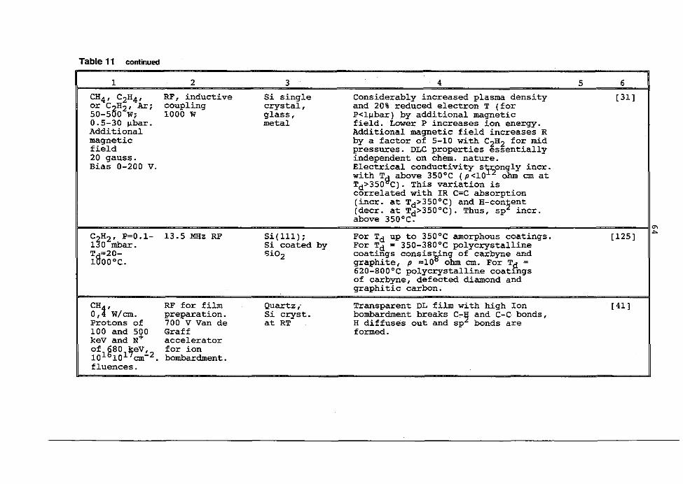
Table 11 continued
'"..
1 2 3 4 5 6
CH4, C2H4, RF, inductive 5i single Considerably increased plasma density [31]or CaH2 I .Ar i coupling crystal, and 20% reduced electron T (for50-SOW; 1000 W glass, P<l~bar) by additional magnetic0.5-30 I1bar. metal field. Lower P increases ion energy.Additional Additional magnetic field increases Rmagnetic by a factor of 5-10 with C2H2 for midfield pressures. DLCproperties essentially20 gauss. independent on chem. nature.Bias 0-200 V. Electrical conductivity sJ20ngly incr.
with Tg above 350·C (p.<10 ohm em atTd>350 C). This variation iscorrelated with IR C=C absorption(incr. at Td>3500C) and H-con2ent(deer. at Td>350°C). Thus, sp incr.above 350·C. ,
C3H2, P=O.l- 13.5 MIIz RF Si(l11); For Td up to 350°C amorphous coatings. [125]1 0 mbar. Si coated by For Td = 350-380·C po1ycrysta11ineTf20- 8i02 coatings consis~ng of carbyne and1 OO·C. graphite, p =10 ohm em. For Td =
620-800·C po1ycrystalline coat~ngs
of carbyne, defected diamond andgraphitic carbon.
CHf
RF for film Quartz,- Transparent DL film with high Ion [41]0, W/em. preparation. Si cryst. bombardment breaks C~~ and C-C· bonds,Protons of 700 V Van de at RT H diffuses out and sp bonds are100 and 5~0 Graff formed.keV and N acceleratoroflg801~ev!2 for ion10 10 em . bombardment.fluences. .
Table 11:
Designations: dc = direct current; EgMH = microhardness; R =
RH = relative humidity;
VB = self-bias voltage;
watt and tungsten).
= optical gap; IR = infrared; = wavelength;
deposition rate; RF = radio frequency;
Ta = annealing temperature; Td = deposition temperature;
W = power (note that the same symbol is used to designate
Abbreviations: abs. = absorption; chern. = chemical; coef. = coefficient; compres. = compression;
canst. = constant; deer. = decrease; depose = deposition, deposited;
dia = diameter; excel. = excellent; incr. = increase; independ. = independent;
max. = maximum; opt. = optical; prod. = production; resp. = respectively.'"ct
66
therefore, if it is sufficiently high (e.g. in thicker films),
the layers tend to delaminate or peel off the substrate.
It has been established that the films containing the highest
concentration of sp3 bonded carbon exhibit highest stress,
while the polymerlike films are low-stressed [25].
The interpretation of the stress seems to be still rather
obscure. Heavy ion bombardment during deposition is an apparent
cause, but structural and compositional effects are superposed,
as is indicated by a maximum in the stress values at a certain
bias voltage, i.e. at a certain ion energy [34].
Adhesion of the films is strong to carbide-forming
substrates, which can be explained by the experimentally found
formation of an interfacial carbide layer on crystalline Si and
Ge [59].
A very broad range of electrical resistivity values (from
1 ohm cm to 10 14 ohm cm [32,15,98,46,30,7,6] was found for RF
plasma deposited coatings, but values in the range 10 9_10 12 ohm
cm seem to be most frequently reported. Dependence on deposition
rate, i.e. on the discharge power, has been found, the lower the
power (and, consequently, the lower the deposition rate), the
higher the resistivity; however, different resistivity intervals
were found by different researchers for similar power or
deposition rate.
The substrate temperature (Td) was found to have a
pronounced effect on electrical resistivity [52,83], the latter
decreasing rapidly with increasing Td' A decrease in resistivityfrom 1011 to 10 3 was produced by temperature increase of only
50 0C (from 250 to 300 oC). This effect, as well as the effect of
substrate potential on resistivity (resistivity decreases with
VB) is related to hydrogen content which decreases with
increasing VB and Td [83].
The hydrocarbon gas (CH4, C2H6, C2H2 or C2H4) influences
the resistivity, which differs up to a factor of about 3 for
the coatings prepared from methane and ethylene at Td=250oC
(resistivity(methane)/resistivity(ethylene) > 10 3) [52].
Good insulating properties of the coatings are ascribed
to saturation of dangling bonds by hydrogen [34].
67
For very thin films « 50 nm) electrical resistivity was
found to increase exponentially with decreasing film thickness
[44]. This effect is due to the fact that thinner films are
closer to the ideal amorphous state. Doping of the coatings with
elements of group III and V of the periodic system was effected
using B2H6 (for B) and PH3 (for Pl. Doping with N, Ta and Ru has
also been reported [34].
Optical properties, namely absorption, transparency and
reflection, are essential from the viewpoint of application for,optical components. It has been found that films produced at
different self-bias voltage change their colour from pale yellow
to black, showing that the short-wavelength optical absorption
edge (Eg) shifts to longer wavelength with increasing VB [17].Low absorption in the red and infrared part of spectrum,
and its virtual disappearance above the wavelength of about
1.5 ~m, is suitable for use of the films as antireflection
coatings for Si and Ge. Absorption measurements at 10.6 ~m on
the coatings prepared from C2H4' C2H6 and CH4 on Ge, have given
values of a few percent per ~m, indicating suitability for the
application as antireflection coatings on Ge [17]. This was
confirmed for the DL films on Ge showing high transparency in
the 3-12 ~m range, but also for a 2.5 mm-thick blank quarter
wave DLC layer on both sides, which had transparency 96-97% in
the 3-5 ~m range [120]. Using the fact that colour of the DL
films depends on their thickness a "colour chart" [80] was
made for thickness ranging between 30 and 270 nm on Si-wafers
prepared by RF plasma decomposition from butane. An additional
interesting characteristic of DL layers is their low friction,
with sliding friction coefficients varying from 0.01 to 0.3,
depending on (increasing with) relative humidity [32,33,34].
In the experiments of sliding friction of steel against DLC
coated Si [34], the friction coefficient had a value of only
0.02 in vacuum or very dry nitrogen. An increase in relative
humidity from 10 to 99% was found to lead to an increase of
friction coefficient from 0.05 to 0.3. An explanation of these
results is based on the fact that DL layers evolve hydrogen when
heated above 300°C, so that there is gas effusion during sliding
68
of the steel against the layer, the gas providing a "cushion" on
which the steel ball can skim.
Instead of using cooled substrate, as reported in majority
of the papers dealing with RF plasma deposition, higher
substrate teperature combined with C2H2 plasma resulted first
(at Td up to 350°C) in amorphous coatings, then in poly
cristalline films consisting of carbyne and graphitic phase
(Td between 350 and 380°C), while at Td between 620 and 800°Ccarbyne, defected diamond and a graphitic carbon were produced
[125]. According to the authors, carbyne is the result of
deposition of the -C=C-radicals produced from acetylene and
their subsequent polymerisation. At higher Td the radicals
dissociate and presence of H atoms allows deposition of the
diamondlike carbon. The authors conclude that in order to obtain
better defined carbyne and diamond films (without graphite) it
is necessary to apply an accelerating voltage on the substrate.
In addition to the high-frequency RF plasma (frequency in
the MHz range, typically 13.56 MHz), used by a great majority
of authors, some authors have used a low-frequency RF plasma
with a frequency range 25-125 kHz [22,110].
These two plasma types differ essentially with respect to
the ability of ions to follow the voltage changes: in the high
frequency RF the ions can not follow the electrical field
changes, but in the low-frequency RF the ion flux reflects time
dependence of the plasma potential. Plasma pressures are also
quite different according to the studies by emission spectro
scopy [22]. However, in spite of these differences, properties
of the carbon films, obtained with high impact energies of the
film forming particles are independent on the type of discharge
used [22].
RF plasma CVD of diamond coatings
Although many researchers have used RF plasma CVD to
deposit carbon coatings, the coatings obtained had properties
which approached more or less to those of diamond, but never
69
reached them. It is only recently that preparation of diamond
coatings by means of this method is reported [69,121,74].
Comparing the conditions of diamond preparation using
the microwave plasma and hot filament CVD methods (see 3.2.3
and 3.1.2, respectively) with those of diamondlike coatings
preparation using the RF plasma CVD, it can be seen that the
main difference consists in substrate temperature range and
initial gas (and, consequently, plasma) composition.
The substrate temperature in both microwave plasma .and
hot filament methods was between 700 and 1000°C, while in the
RF plasma it was not far from the room temperature.
Concerning the initial gas, it consisted in the case of
the former methods of a low concentration of a hydrocarbon in
hydrogen, resulting in high concentration of atomic hydrogen
in the plasma, while in the RF plasma method no hydrogen was
present in the initial gas mixture. It is these two parameters,
substrate temperature and gas/plasma composition, that are
changed in the mentioned recent RF plasma studies [69,121,74],
making them similar to those in the microwave plasma and hot
filament methods and enabling the authors to produce diamond
coatings.
A schematic diagram of the apparatus used for diamond
coatings deposition (Fig. 18) [121] shows that it contains
the same main components as those used to obtain diamondlike
coatings. RF power is supplied from a 13.56 MHz generator
through an impedance matching network terminating the working
coil. The substrate is brought to the necessary temperature
(700-1000 0C) by inductive heating and energy transfer of the
plasma, i.e. without any additional heating.
The hydrocarbons used were CH4, CO, CH30H, C2H50H,
CH3COCH3' C6H12 and C6H6 and their concentrations in hydrogenwere up to 2%. In order to increase atomic hydrogen content in
the plasma, high RF power was used.
The substrates used were Si wafers, Mo and quartz/silica.
Their polishing [69] and, in some cases, preliminarly coating
by a DL layer [74] resulted in a higher nucleation density [69].
Table 12 contains data relative to RF plasma deposited
diamond coatings.
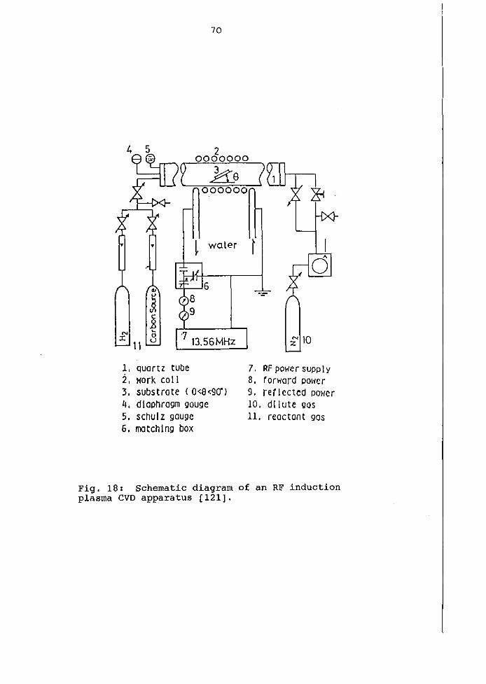
70
Z 10
~ water r
'7 13.56MHz
? ke000000
t; 5 20000000
•
j.8
N ~
:c 011 u
1, quartz tube2, wark call3, substrate (0<8<90")4. diaphragm gauge5. schulz gauge6. matching bax
7. RF power supply8, forward oouer9. reflected power10. dilute 90S
11. reactant 9as
Fig. 18: Schematic diagram of an RF inductionplasma CVD apparatus [121].
71
The methods used to characterize the deposits were SEM
[69,121,74], electron diffraction [69,121], Raman spectroscopy
[121], XPS [121], Auger spectroscopy [74], IR spectroscopy
[121], measurement of electrical resistivity and microhardness
[69] .Growth rate and dependence of crystal shapes on deposition
conditions were found to be similar to those in the hot filament
method. A suitable substrate temperature was found to be 700
800·C (above this temperature graphite appears) [121], 700
1000·C [74] and below 950·C [69].
Properties of the obtained diamond films are high hardness
(80-90 GPa [121], 70-120 GPa [69]), high electrical resistivity(10 8_1 010 ohm cm) [69] and good adherence [69].
According to [74] RF plasma CVD has the advantage over
microwave system in that it can be easily scaled to large volume
and high power.
In a variant of RF plasma CVD [108], CH4 is not introduced
into the hot plasma region, but downstream from a He discharge.
A low pressure (around 13 ~bar) and low RF power (80 W) havebeen used. Metastable He, formed in the inductively coupled
discharge region is transported towards the substrate, and
diluted CH 4/He mixture (2-20%) is separately introduced into
the substrate region. The excited He atoms interact with CH4
molecules, causing dissociation into CHx or CHx + radicals, which
condense on the substrate heated up to 7l5·C. Short residence
time (i.e. high low-rate, amounting to 30 l/h) and low CH4
concentration prevent any gas phase polymerization, so that
gas-solid reactions predominate. Diamond layers are produced,
but they contain disordered graphitic carbon.
In conclusion, the RF plasma CVD can be used to produce
diamond coatings. In order to do so it is necessary to have low
concentration of hydrocarbon in hydrogen and high substrate
temperature (700-1000·C). High power results in higher atomic
hydrogen concentration. Polishing with diamond paste enhances
nucleation.
However, the available literature data are insufficient
to permit definite conclusions about the advantages or
disadvantages of this method with respect to other methods
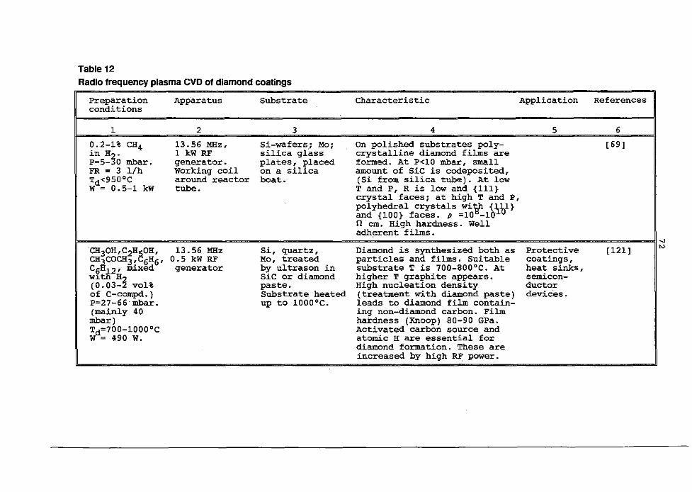
Table 12Radio frequency plasma CVD of diamond coatings
Preparation Apparatus Substrate Characteristic Application Referencesconditions
1 2 3 4 5 6
0.2-1% CH4 13.56 MHz, 5i-wafers,; Mo; On polished substrates poly- [69]in Hr 1 kW RF silica glass crystalline diamond films areP=5- 0 mbar. generator~ plates, placed formed. At P<lO mbar, smallFR = 3 llh Working coil on a silica amount of SiC is codeposited,Td<950oC around reactor boat. (5i from silica tube). At lowW = 0.5-1 kW tube. T and P, R is low and {Ill}
crystal faces; at high T and P,polyhedral crystals wiJl> {lV}and {100} faces. p =10 -10n em. High hardness. Wellad.h~rent films.
CH30H,C2H~OH, 13.56 MHz Si, quartz, Diamond is synthesized both as Protective [12lJCHaCOCH3, 6H6' 0.5 kW RF Mo, treated particles and films. Suitable coatings,C6cli2, mixed generator by ultrason in substrate T is 700-800°C. At heat sinks,w~ H~ SiC or diamond higher T graphite appears. semicon-(0.03- vo1% paste. High nucleation density ductorof C-compd.) Substrate heated (treatment with diamond paste) devices.P=27-66mbar. up to 1000oC. leads to diamond fi~ contain-(mainly 40 ing non-diamond carbon. Filmmbar) hai:dness (Knoop) 80-90 GPa.Td=700-l000oC Activated carbon source andW = 490 W. atomic H are essential for
diamond formation. These areincreased by high ~ power.
-oJ
'"
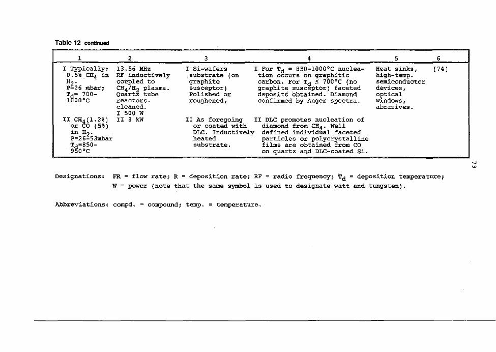
Designations: FR = flow rate; R = deposition rate; RF = radio frequency; Td = deposition temperature;
W = power (note that the same symbol is used to designate watt and tungsten).
II As foregoingor coated withDLC. Inductivelyheatedsubstrate.
Table 12 continued
1
I Typically:0.5% CH4 inHZ'P=Z6 mbar,Td = 700llJOOoC
II CH4 ( l. Z%)or CO (5%)in HZ'P=Z6-53mbarTd=850950°C
Z
13.56 MHzRF inductivelycoupled toCH4 / HZ plasma.Quartz tubereactors.cleaned.I 500 WII 3 kW
3
I Si-waferssubstrate (ongraphiteSllsceptor)Polished orroughened,
4
I For Td = 850-1000°C nucleation occurs on graphiticcarbon. For Td S 700°C (nographite susceptor) faceteddeposits obtained. Diamondconfirmed by Auger spectra.
II OLe promotes nucleation ofdiamond from CH4. Welldefined individual facetedparticles or polycrYstallinefi~s are obtained from COon quartz and OLe-coated Si.
5
Heat sinks,high-temp.semiconductordevices,opticalwindows,abrasives.
6
(74)
...,w
Abbreviations: compd. compound; temp. temperature.
74
of diamond coating preparation (coating quality, possibility
of using different substrate materials etc.)
3.2.3 Microwave plasma chemical vapour deposition (CVD)
of diamond and diamondlike coatings
Diamond coatings
Microwave plasma CVD of carbon coatings, a new method
developed during the last several years, enabled researchers
from different centers in the world to obtain well-defined
diamond layers. Indeed, one of the very first methods found
to produce well crystallized diamond used a 2.45 GHz microwave
power source to produce a glow discharge plasma in mixturees
of 1-3% methane in hydrocarbon and at gas pressures of 10 to
80 mbar [53].
Several crucial parameters are combined in the method:
- A suitable gas mixture, consisting of a low concentration
of a hydrocarbon gas (CH4) in hydrogen (H2);
- High ionization efficiency of the plasma (higher than in
the diode-type sources [13]) providing suitable species for
diamond deposition, in particular high concentracion of atomichydrogen;
- Substrate temperature in the range 700-1000°C;
- Substrate surface containing seed diamond particles,
carbides or carbide-forming metals.
The fact that microwave (MW) plasma CVD (MWPCVD) is an
electrodeless discharge was stated as an additional advantage of
the method, because no (otherwise unavoidable) contamination is
introduced by the electrode material. However, according to [11]
the MWPCVD produces very reactive species (like atomic hydrogen)
which can react with the Si02 tube wall placed in the MW cavity,
as well as with the substrate and its holder, thus introducing
impurities into the deposit.
Typical apparatus and working conditions are described
below [11]. The MWPCVD system is comprised of several smaller
units as shown in Figs. 19 and 20 which include: the gases
75
(5% CH4 in H2' H2 and Ar), the gas flow control, the MWgenerating equipment, the reaction chamber, the pressure control
and the pump. The two major components of the system discussed
below are the MW generating equipment and the reaction chamber.
The MW system is shown in Fig. 19. The microwave generator
may be operated at powers between 0.1 and 1.5 kW at a frequency
of 2.45 GHz. Confining the microwaves is a set of waveguides
attached to the generator. Four of the waveguide components have
additional functions. First, the isolator allows microwaves to
pass through from the generator, but protects the generator by
absorbing the reflected microwaves. Secondly, the reflected
power is monitored by the power monitor. Minimization of the
reflected power is required, and is achieved by adjusting the
next waveguide component, the three-stub tuner. Finally, the
microwaves interact with the reaction chamber in the water
cooled applicator.
The reaction chamber consists primarily of a vertically
mounted fused quartz tube, 3.8 cm o.d. and 76 cm long, which
confines the plasma. Figure 20 is an illustration of the
reaction chamber, but also includes the gas flow and pressure
control systems. The reactant gases, methane (CH4) and hydrogen
(H2), flow through the gas inlet at the top of the reaction
chamber. Also, located at the top of the reactor is a glass
viewport used to observe the progress of the deposition and to
measure the substrate temperature with an optical pyrometer.
Because of the interference of the plasma, the substrate
temperature obtained may not be the actual temperature and
caution must be taken.
Flowing from the inlet, the CH4 and H2 reactant gases
enter the fused quartz tube where the gases interact with the
microwave energy in the applicator which creates a plasma
confined within the quartz tube. A film is deposited by the
activated gases onto a single-crystall silicon (100) substrate.
The height of the substrate in relation to the plasma may
be adjusted by an alumina substrate holder assembly. Also, the
substrate is heated only by the interaction with the microwave
power and the plasma; no external heating is used. The reactant
gases finally flow out of the bottom of the reaction chamber

76
GAS FLOWCONTROl.
MICROWAVEGENERATOO
ISOLATORo MICROWAVE
AF'PLICATOR(WATER-COOL£D)
REACTIONCHAMBER
.L
POWER MONITOO;INDICATOR--------,
III
Fig. 19: Schematic diagramgenerating equipment [11].
of a microwave
GLASSVIEWPORT
CAPACITANCE:~A.wlo!..EIQl: I
,,,,
MICROWolVl;'APPl.lCATOR{WATER COOLEOI
FUSro QuARTZTUSING
'"Ih'l..ET
, i :.c",,, I I
·~I
GJ I J
~It;;\ MASS FLOfi iL.:J METER !
HEIGHTADJUSTA8LESU8STRATE
PROCAAM PRI;SSUREDISPlAY CONTROl.llR
D-Q
b'='=frr;n.--K'7V77 TO
FF"-J--'-~?,;--;;~,*,~ PUMf
Fig. 20: Schematic diagram of a microwave plasmaCVD reaction chamber, gas flow control and pressurecontrol [11].
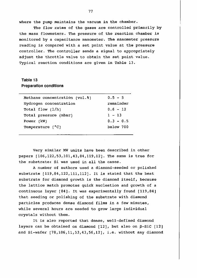
77
where the pump maintains the vacuum in the chamber.
The flow rates of the gases are controlled primarily by
the mass flowmeters. The pressure of the reaction chamber is
monitored by a capacitance manometer. The manometer pressure
reading is compared with a set point value at the pressure
controller. The controller sends a signal to appropriately
adjust the throttle valve to obtain the set point value.
Typical reaction conditions are given in Table 13.
Table 13
Preparation conditions
Methane concentration (vol.%)
Hydrogen concentration
Total flow (l/h)
Total pressure (mbar)
Power (kW)Temperature (0C)
0.5 - 5
remainder0.6 - 12
1 - 13
0.3 - 0.5
below 700
Very similar MW units have been described in other
papers [106,122,53,101,43,84,119,12]. The same is true for
the substrate: Si was used in all the cases.
A number of authors used a diamond-seeded or polished
substrate [119,84,122,111,112]. It is stated that the best
substrate for diamond growth is the diamond itself, because
the lattice match promotes quick nucleation and growth of a
continuous layer [84]. It was experimentally found [119,84]
that seeding or polishing of the substrate with diamond
particles produces dense diamond films in a few minutes,
while several hours are needed to grow large individual
crystals without them.
It is also reported that dense, well-defined diamond
layers can be obtained on diamond [12], but also on P-SiC [12]
and Si-wafer [78,106,11,53,43,56,12], i.e. without any diamond
78
present. This is explained by the lattice matching of P-SiC
(also formed on the surface of Si) with respect to diamond [12].
The experimentally found nucleation on highly-oriented graphite
[12] is also ascribed to the presence of P-SiC, which is formed
by reaction of graphite with Si coming from the Si02 walls of
the reactor due to etching by atomic hydrogen.
On a Ni surface only amorphous carbon was obtained, but
nucleation of diamond becomes possible if gaseous Si species are
present [12]. Fused silica [106,12] and Ti [84] were also used
as substrates. It follows from these and other experimental
results that carbide-forming elements are suitable for diamond
nucleation.
Dilute mixtures of CH4 in H2 were used by majority of the
authors, the CH4 concentration varying from 0.1 to 10%. Working
pressures used were in the range 1-120 mbar, while the substrate
temperature was varied from 600 to 1200 oC.
Unlike in the other papers, preparation of diamond films
from the vapours of different organic compounds (CH4, CH30H,C2H50H, CH 3COCH3) has also been reported [111,112]. The diamond
films obtained contain sp2-bonded carbon, as evidenced by the
Raman spectroscopy (1550 cm- 1 peak), but its amount can be
reduced by choosing suitable working conditions: one of the
alcohols as a starting compound, low concentration in H2 (O.5%),
6-26 mbar pressure, Td=850-950°C.
The role of total pressure has not been investigated above
120 mbar. According to Kawarada [126], above 5.3 mbar deposition
of crystalline diamond predominates, while at lower pressures
the deposits contain significant quantities of graphite or SiC.
It has been also reported [12] that pressure between 50 and
120 mbar, combined with other optimum experimental conditions
(Td=975-1000°C, CH4/H2=0.2-0.5%, FR=6 I/h), rather than
1-13 mbar used in an earlier study [11] allows formation of
well defined diamond crystals.
Concerning the deposition rate, it was found to vary
in a broad range, from 30 nm/h to 3 ~m/h, i. e. two orders
of magnitude (see Table 14). It depends on CH4 concentration,
increasing with it, but contamination with sp2 carbon also
increases [84]. It was found that an addition of less than
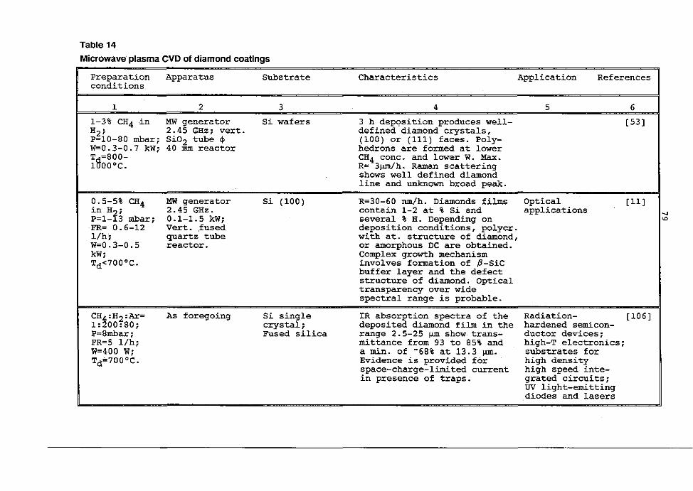
Table 14
Microwave plasma eVD of diamond coatings
...,'"
Preparation Apparatus Substrate Characteristics Application Referencesconditions
1 2 3 4 5 6
1-3% CH4 in MW generator 8i wafers 3 h depqsition produces well- [53]H2; 2.45 GHZi vert. defined diamond crystals,P=10-80 mbar; Si02 tube ~ (100) or (111 ) faces. Poly-W=O.3-0.7 kWi 40 rom reactor hedrons are formed at lowerTf800- CH4 conc. and lower W. Max.100°C. R= 3lUll/h. Raman scattering
shows well defined diamondline and unknown broad peak.
0.5-5% CH4 MW generator Si (100) R=30-60 nm/h. Diamonds films Optical [11]in H • 2.45 GRz. contain 1-2 at % Si and applicationsP=l-f3 mbar; 0.1-1.5 kW; several % H. Depending on ,FR= 0.6-12 Vert. ,fused deposition conditions, polycr.1/h; quartz tube with at. structure of diamond,W=0.3-0.5 reactor. or amorphous DC are obtained.kWi Complex growth mechanismTd<700°C. involves formation of ~-SiC
buffer layer and the defectstructure of diamond. Opticaltransparency over widespectral range is probable.
CRfR2:Ar= As foregoing Si single IR absorption spectra of the Radiation- [106]1: 00:80; crystal; deposited diamond film in the hardened semicon-P=8mbarj Fused silica range 2.5-25 ~ show- trans- ductor devices;FR=5 l/h; mittance from 93 to 85% and high-T electronics;W=400 W; a min. of -68% at 13.3 lUll. substrates forTd=700°C. Evidence is provided for high density
space-charge-limited current high speed inte-in presence of traps. grated circuits;
UV light-emittingdiodes and lasers
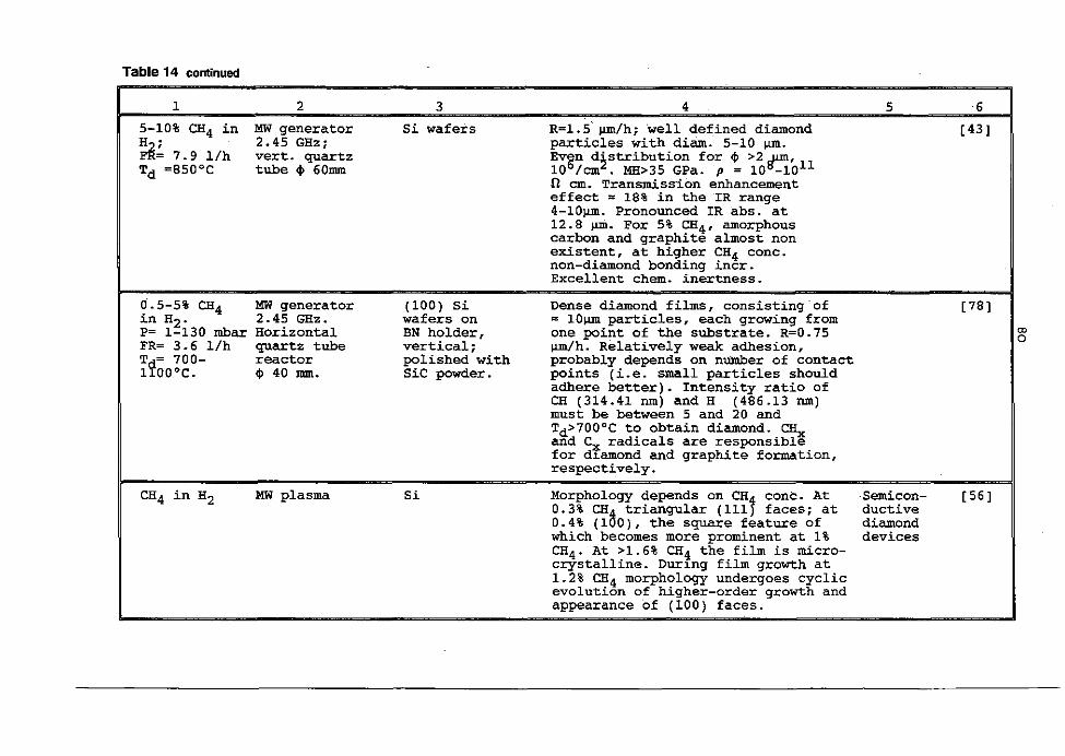
Table 14 continued
1
5-10% CH4 inH .F~':' 7.9 1/hTd =850°C
0.5-5% CH4in H2.P= 1-130 mbarFR= 3.6 l/hTd= 7001IOO°C.
CH4 in HZ
2
MW generator2.45 GRz;vert. quartztube <I> 60_
MW generator2.45 GHz.Horizontalquartz tubereactor<I> 40 JIDII.
MW plasma
3
8i wafers
(100) Siwafers onBN holder,vertical;polished withSiC powder.
Si
4
R=1.5 ~/h; well defined diamondparticles with diam. 5-10 ~m.
Ev6n d~stribution for ¢ >2~,10 lern • MH>35 GPa. p = 10 _lOlln em. Transmiss~on enhancementeffect = 18% in the IR range4-10~. Pronounced IR abs. at12.8 ~. For 5% CH4, amorphouscarbon and graphite almost nonexistent, at higher CH4 conc.non-diamond bonding incr.Excellent chem. inertness.
Dense diamond fi~s, consisting"of= 10~ particles, each growing fromone point of the substrate. R=0.75~h. Relatively weak adhesion,probably depends on number of contactpoints (i.e. small particles shouldadhere better). Intensity ratio ofCH (314.41 nm) and H (486.13 nm)must be between 5 and 20 andTd >700°C to obtain diamond. CHxand C~radicals are responsiblefor d1amond and graphite formation,respectively.
Morphology depends on CH4 cone. At0.3% CH4 triangular (Ill) faces; at0.4% (100), the square feature ofwhich becomes more prominent at 1%CH4. At >1.6% CH4 the film is microcrystalline. Dur~ng film growth at1.Z% CH4 morphology undergoes cyclicevolution of higher-order growth andappearance of (100) faces.
5
Semiconductivediamonddevices
6
[43]
[78]
[56]
ex>o
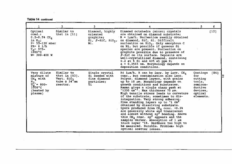
Table 14 continued
co~
1 2 3 4 5 6
Optimal Similar to Diamond, highly Diamond octahedra (micro) crystals [12]condo : that in [11] oriented are obtained on diamond substrate;0.2-0.5% CH4 graphite; R ~ 11ll1l/h. Nucleation readily obtainedin H . Si, j9-SiC, 5i02 1 on diamond, SiC, Si. Difficultp~ 53:120'mbar Ni. nucleation on SiO
I"Only amorphous. C
FR~ 6 l/h on Ni, but possib e if gaseous 5iTf 975- species are present. Nucleation on100°C graphite possible due to presence ofw~ 300-400 W P-SiC on its surface. Deposits are
well-crystallized diamond, containing0.2 at % Si and 435 at ppm H;a = 0.3565 run. Morphology depends ondeposition conditions.
Very dilute Si..mi.lar to Single crystal R:S 11ll1l/h. R can be incr. by incr. CH4 Coatings [84]mixture of that in [53]. 5i seeded with conc., but contamination also iocr. for (
CH4 with Vert. Si02 fine diamond Po1ycr. diamond layers, with grains cuttingH2 . tube 4> 34 rom particles; up to 10 1llIl. Morphology depends on tools,Tg ~ 800- reactor. Ti growth conditions and substrates. semicon-100°C Raman givrs a single sharp peak at duative(heated by -1330 cm- . Max thickness 70 1llIl. deVices,plasma) High tensile stress leads to curvature optical
of the substrate, sometLmes to dis- elements.in~eg~ation. Very strong adhesio~.
. Free standing layers, up to -1 emobtained by dissolving substrate.Lyers produced from CHaconc. <0.3%are generally white a~ translucentand almost withou~ sp bonding. Abovethis CH4 cone. sp appears and thesamples darker. Absorption of 1 IllIlthick layer -1%. Hardness too high" tobe measured. Durable,. Problem; highoptical" scatter losses .
.
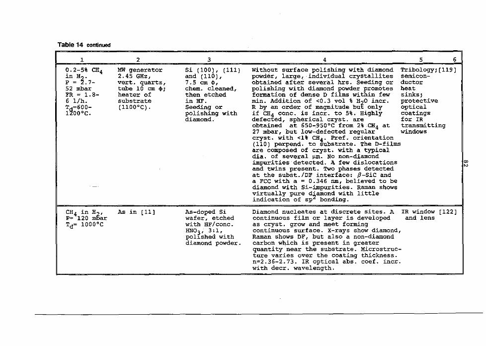
Table 14 continued
ce
'"
1 2 3 4 5 6
0.2-5% CH4 MW generator Si (100) r (111 ) With~ut surface polishing with diamond Tribology; [119Jin Hr 2.45 GHz, and (110), pOWder, large, -individual crystallites semicon-p = .7- vert. quartz, 7.5 em q" obtained after several hrs. Seeding or ductor52 mbar tube 10 em q,; chem. cleaned, polishing with diamond powder promotes heatFR = 1.8- heater of then etched formation of dense D films within few sinks;6 l/h. substrate in HF. min. Addition of <0.3 vol % H~O incr. protectiveTq~600- (1100°C) . Seeding or R by an order of magnitude bu only optical100°C. polishing with if CH4 cone. is incr. to 5%. Highly coatings
diamond.· defected, spherical cryst. are for IRobtained at 650~950°C from 2% CH4 at transmitting27 mbar, but low-defected regular windowscryst. with <1% CB4 0 Pref. orientation(110) perpend. to substrate. The D-filmsare composed of cryst. with a typicaldia. of several J.I..IIl. No non-diamondLmpurities detected. A few dislocations (
and twins present. Two phases detectedI
at the subst./DF interface: {i-SiC anda FCC with a = 0.346 nm, believed to be
- diamond with Si-~purities. Raman showsvirtually pure d~amond with littleindication of sp bonding.
CH4 in ~' As in [11] As-doped Si Diamond nucleates at discrete sites. A IR window [122]p= 120 ar wafer, etched continuous film or layer is developed and lensTd= 1000°C with HF/conc. as cryst. grow and meet forming
HN03, 3:1, continuous surface. X-rays show diamond,pohshed with Raman shows DF, but also a non-diamonddiamond powder. carbon w~ich is present in greater
quantity near the substrate. Microstruc-ture varies over the coating thickness.n=2.36-2.73. IR optical abs. coef. incr.with deer. wavelength.
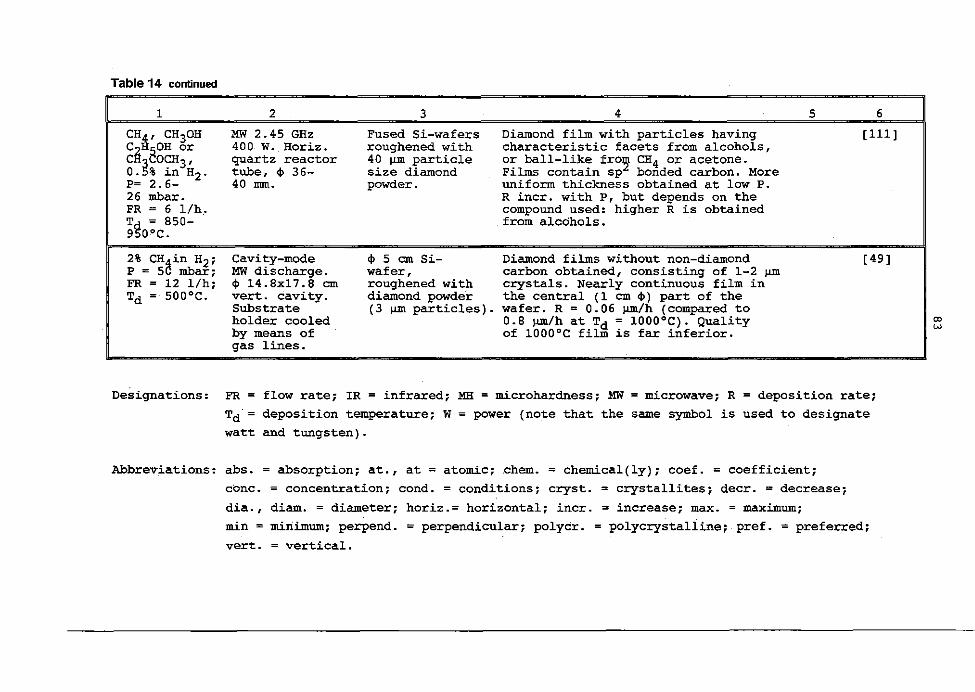
Table 14 continued
1 2 3 4 5 6
CH~, CH30H MW 2.45 GHz Fused Si-wafers Diamond film with particles having [111]~ tH or 400 W. Horiz. roughened with characteristic facets £rom alcohols,
~ OCH3, quartz reactor 40 IJ.lll particle or ball-like fro~ CH4 or acetone.O. % in H2. tube, <I> 36- size diamond Films contain sp bonded carbon. Morep= 2.6- 40 mm. powder. uniform thickness obtained at low P.26 mbar. R incr. with P, but depends on theFR = 6 l/h. compound used: higher R is obtainedTg = 850- from alcohols.90°C.
2% CH~in H2 Cavity-mode <I> 5 cm Si- Diamond fiLms without non-diamond [49]P=5 mbar MW discharge. wafer, carbon obtained, consisting of 1-2 ~FR = 12 l/h <I> l4.8x17.8 em roughened with crystals. Nearly continuous film inTd = 500°C. vert. cavity. diamond powder the central (1 em <1» part of the
Substrate (3 IJ.lll particles). wafer. R = 0.06 IJ.lll/h (compared toholder cooled 0.8 IJ.lll/h at Td = 1000°C). Qualityby means of of lOOO°C film is far inferior.gas lines.
ccco
Designations: FR = flow rate; IR = infrared; MH = microhardness; MW
Td"= deposition temperature; W = power (note that thewatt and tWlgsten).
microwave; R = deposition rate;
same symbol is used to designate
Abbreviations: abs. = absorption; at., at = atomic; chem. = chemical(ly); coef. = coefficient;
conc. = concentration; condo = conditions; cryst. = crystallites; decr. = decrease;
dia., diam. = diameter; horiz.= horizontal; incr. = increase; max. = max~um;
min = minimum; perpend. = perpendicular; po.Lycz , = polycrystalline; pref. = preferr'ed;
vert. = vertical.
84
0.3% H20 provoked an increase of deposition rate by one order of
magnitude, although only if CH4 concentration was also increased
[119]. This is thought to be due to production of OH and 0 which
aid decomposition of CH4, the oxygen simultaneously preventing
(by etching) formation of non-diamond deposits.
In all the papers formation of diamond was reported, its
structure varying from amorphous to polycrystalline [11], often
with well defined particles (crystals) [53,43,84,119,56,78,12]
of up to 10 ~m diameter [43,84,78], the diamond being identified
by electron diffraction [11,119,53], reflection high-energy
electron diffraction (RHEED) [78], X-ray diffraction [122,78,
12], SEM and/or TEM [119,84,53,56,12], Raman spectroscopy
[84,119,122,43,53,12].
Crystallinity, morphology and preferred orientation were
found to depend on deposition conditions [119,84,53,56,12],
namely CH4 concentration, substrate nature and power.
In addition to deposition temperature which must be
higher than 700°C, intensity ratio of the emission lines of CH
(at 314.41 nm) and Hp (at 486.13) was found to have a crucial
importance for diamond deposition [78]. This ratio must be
between 5 and 20. Generally, CHx and Cx radicals are considered
resposible for diamond and graphite formation, respectively
[78] .
In order to reduce the substrate temperature with respect
to the typically used range (700-1000°C) and thus allow use of
lower-temperature-melting substrate materials, the substrate
exposed to a new cavity-type plasma was cooled by means of the
nitrogen gas flowing through a pipe embedded in the substrate
holder [49]. The deposition temperature was reduced to 500°C,
which resulted in a substantially lower deposition rate
(0.06 ~m/h, as compared to 0.8~m/h obtained at 1000°C under
otherwise similar conditions), but well defined diamond films
almost withough non-diamond carbon were obtained. According to
the authors, good quality of the films is a consequence of a
high hydrogen ion and atom density in the plasma and the low
growth rate.
In another study [93] a discontinuous microwave plasma was
used with repeated cycles, in which the substrate was heated up
85
to a final temperature (between 500 and 800°C), held at it for
a certain time and then cooled to room temperature (cooling
intervals are not considered to be within the cycles).
The authors operate with the term llaverage temperature It
during the cycle which is lower than the final temperature and
amounts to about 400°C. This technique enabled the authors to
control diamond nucleation and to obtain films with fine grain
size and surface roughness of the order of 5 to 20 nm, thus
reaching the optical transparency above 60% in the 0.6-2 ~m
wavelength range, comparable to natural diamond.
The complex growth mechanism was found to involve
formation of a "buffer layer" on the substrate/layer interface
[11,119]. This is composed of ~-8iC and a face-centered cubic
phase with a=0.346 nm, which is believed to be defected diamond
containing 8i impurities. It has been suggested [119] that these
phases might facilitate the transition from pure 8i to pure
diamond through intermediate compounds.
The adherence of the diamond layers to the substrate is
generally excellent, but associated with high tensile stresses,
leading to the curvature of the substrate and sometimes to
disintegration [84]. Interpreting results obtained by means of
the X-ray topographic technique [85], the authors conclude that
narrow cracks, as well as residual strain (due to the coherent
contacts with the substrate) are present in the 20 ~m thick
diamond film. It was reported [78], however, that the adherence
of a layer grown on the 8iC-polished-8i-wafer was poor, because
in this case each diamond particle was found to be in contact
with the substrate only at the point which was the vertex of
the single crystal.
Microhardness of the diamond layers was reported to be
higher than 35 GPa [43], or too high to be measured by Knoop
indenter [84].
A number of papers is concerned with optical properties
of the diamond layers, primarily in the IR region [106,11,43,
122,119,84]. Transmittance in the range from 2.5 to 25 ~m is
high, amounting to 85-93% and showing a minimum of 68% at
13.3 ~m [106]. Transmission enhancement effect of about 18%
86
was found in the range 4-10 ~m, pronounced absorption being at
12.8 ~m [43).
IR optical absorption coefficient was found to increase
with decreasing wavelength [122). Because of the nature of the
polycrystalline morphology of the layers, they have optical
scatter losses suspected to be a primary source of the energy
loss with unpolished CVD diamond coatings [122).
Optical properties in the visible part of the spectrum
depend on the presence of non-diamond carbon phases, which in
turn depends on deposition conditions. The layers grown from low
CH4 concentration «0.3%) are generally white and translucent
and their Raman spectra show almost complete absence of sp2
bonding. Higher CH4 concentration leads to darker and less
translucent layers, in which the presence of sp2 bonds is
apparent in the Raman spectra [84).
The effective refractive index of the diamond layers was
found to vary from 2.36 to 2.73 [122).
Electrical resistivity of the diamond film was reported to
vary from 10 8 to 1011 ohm cm, decreasing with the amount of
amorphous carbon [43).
By using a mixture of CH4 (0.3%) and diborane (0.136-4.80
ppm) with hydrogen under the conditions used in [53), B-doped
diamond films showing semiconductive properties were epitaxially
grown on diamond single-crystal substrates [54). The B/C ratio
in the films is related to B concentration in the starting gas
mixture. The electrical conductivity of the B-doped films
increases exponentially with substrate temperature.
The diamond films were found to have excellent chemical
inertness [43), which agrees with the finding that the diamond
layers are durable [84).
In conclussion, it can be said that virtually pure diamond
layers can be grown by the MWPCVD method, with a maximum
deposition rate of the order of 1 ~m/h. The essential deposition
conditions that must be satisfied to obtain diamond deposit are
the gas mixture consisting of hydrogen with a low CH4
concentration at pressures 50-120 mbar and substrate temperature
in the range 700-1000°C (according to [49), the substrate
temperature of 500°C combined with a dense plasma can be used).
87
Although the presence of diamond seed particles on the
substrate is not essential, it certainly has a favourable effect
on the nucleation and growth of the diamond layers. Presence of
carbide forming elements is also suitable for diamond formation.
The optimum values of deposition parameters, in particular
CH4 concentration, remain to be determined. In order to do that,
a better knowledge of the mechanism of nucleation and growth and
of its dependence on the processes in the plasma seems to be
necessary.
Diarnondlike coatings
Although majority of papers concerning the MW plasma CVD
of carbon coatings describes preparation of diamond, formation
of diamondlike coatings has also been reported [70,72,101]
(see Table 15).
The working conditions used were not suitable for "pure"
diamond formation, either because the initial gas mixture did
not contain hydrogen, or because deposition temperature was too
low. However, in one of the papers [70] the deposit obtained
from 5% CH4 in H2 at 700°C contained 1 ~m diamond particles,although their analysis showed presence of a large amount of
hydrogen and small amount of graphitic carbon.
In a study intended to clarify the role played by
hydrogen [72], the DLC formed was exposed to hydrogen plasma.
The graphitic (Sp2 bonded) carbon contained in the coating was
sputtered by plasma to form hydrocarbons and carbon molecules,
but the sp3 bonded atoms were not sputtered. This is in
agreement with earlier conclusions [104]. Formation of CH3radicals with sp3 bonds is considered by the authors to be
resposible for diamond formation, as well as the adsorption
of atomic hydrogen on the deposited carbon.
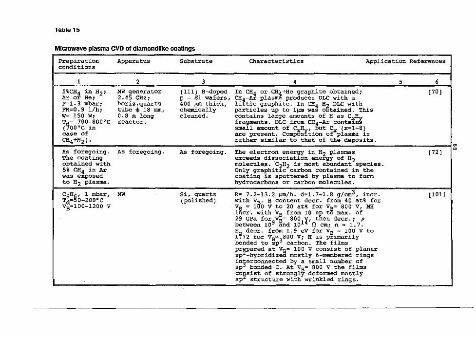
Table 15
Microwave plasma CVD of diamondlike coatings
ex>ex>
Preparation Apparatus Substrate Characteristics Application Referencesconditions
1 2 3 4 5 6
5%CH4 in H2; MW 9.enerator (111) B-doped In CH4 or CH4~He graphite obtained; [70]Ar or He; 2.45 GHz; P ~ 5i wafers, CHt-Ar plasma produces OLe with aP=1.3 mbar; hor.i:.z.quartz 400 ~ thick, li tle graphite. In CH4-HSDLC withFR=0.9 l/h; tube <I> 18 JDIII, chemically particles up to l~ was 0 tained. ThisW= 150 W; 0.8 m long cleaned. contains large amounts of H as c~Tf 700-800°C reactor. fragments. OLe from CH!-Ar conta~n
( OO°C in small amount of C~, ut Cx (x=1-8)case of are present. Compos tion of plasma isCH4+H2) . rather similar to that of the deposits. ,As foregoing. As foregoing. As foregoing. The electron energy in H2 plasmas [ 72]
,The coating exceeds dissociation energy of H2obtained with molecule.s. CZ~2 is most abundant species.5% CH4 in Ar Only graphit~c carbon contained in thewas exposed coating is sputtered by plasma to formto H2 plasma. hydrocarbons or carbon molecules.
C6Hg, 1 mbar, MW Si, quartz R= 7.2-13.2 ~/h. d=1.7-l.8 g/cm3, incr. [lOlJTd= 0-200°C (polished) with Va. H content decr. from 40 at% forVB=100-1200 V VB = 1 0 V to 20 at% for VB= 800 V, MH
incr. with ~ from 10 up to max. of29 GPa for
9.B=800 l ! , then deer.; p
between 10 and 10 . n cm; n = 1.7.Eg deer. from 1.9 eV for VB = 100· V to1.72 for VB= 800 V; H is primarilybonded to sp3 carbon. The filmspr2pared at V~= 100 V consist of planarsp -hybridize mostly 6-membered ringsin~erconnected by a small number ofsp bonded C. At VB= 800 V the filmsco~sist of strongly deformed mostlysp structure with wrinkled rings.
Table 15:
Designations: Eg = optical gap; FR = flow rate; MH = rnicrohardness; MW = microwave;
R = deposition rate; Td = deposition temperature; VB = self-bias voltage;
W = power (note that the same symbol is used to designate watt and tungsten).
Abbreviations: deer. decrease; incr. increase; max. maximum.
co
'"
90
3.2.4 Thermal plasma chemical vapour deposition
In the last several years a new technique of diamond
coating preparation has been introduced, using thermal plasma.
By using high power dc, ac, RF or MW discharge, a high
temperature plasma is obtained.
A substantial difference of such high-temperature plasma
(with gas temperature preferably higher than 2300°C, usually
about SOOOOC) from low-temperature plasma (with gas temperature
~1300°C) is in pressure and concentration of active species
(ions or radicals) which are high in the former and low (maximum
about 10%) in the latter [73]. High temperature is achieved by
using high power. A high concentration of active (excited)
chemical species in thermal plasma is caused by a combination of
collisions with electrons accelerated by the electric field and
collisions of thermodynamically activated species themselves.
Therefore, the rate of diamond growth in the thermal plasma is
high (of the order of 100 ~m/h), compared to that in the low
temperature plasma (maximum of the order of 1 ~m/h).
Because of high temperature, both degree of decomposition
of reactant gases and atomic hydrogen content are high. By
placing the substrate at an appropriate distance from the plasma
and/or applying water cooling, a temperature range 600-1200°C is
obtained, so that conditions for diamond deposition are
achieved.
Synthesis of well-defined diamond films was effected by
means of thermal plasma [71]. This was obtained by using a
plasma torch (4 MHz, 60 kW) at 1 bar with methane introduced
into Ar carrier gas. The substrate was water-cooled Mo plate,
the temperature of which was estimated to be 700-1200°C. The
deposition of polycrystalline diamond film was effected on the
diamond-paste-polished substrate, while polyhedral diamond
crystals 10-30 ~m in size were obtained without polishing.
Very high deposition rate (60 ~m/h for films, 180-300 ~m/h
for single-crystal diameter) were obtained.
Rather similar technique and results have been reported
[61] for a de thermal plasma (dc arc discharge). A mixture of
91
CH4 and H2 is fed between cylindrical anode and cathode rod of
the plasma torch and a plasma jet is generated by dc arc
discharge around the torch nozzle (Fig. 21).
The plasma jet is directed to water-cooled substrate (Si,
Mo, Pt, SiC or silica), the temperature range of which is 500
1200°C. Polygonal diamond crystals are grown in this temperature
range (below and above this temperature a diamonlike film and
graphitic or amorphous carbon are obtained, respectively). Well
crystalline and good-quality diamond layer can be formed at a
growth rate of 80 ~m/h.
Even higher deposition rate (200-250 ~m/h) has been
reported [5] for similar deposition conditions (130-1000 mbar,
typically 260-520 mbar, 1% ethanol in H2' substrate temperature
800-900 0C). The polycrystalline diamond films show rugged (rock
like) surface. The films do not contain non-diamond carbon.
Thus, thermal plasma method appears to be suitable for
diamond deposition. In particular, very high deposition rates
are obtained, differing by at least one order of magnitude
from those obtained by other methods, and high-quality diamond
layers containing no non-diamond carbon are produced.
The method has, however, some disadvantages. It is
difficult to achieve a proper control of deposition temperature.
The films have poor adhesion to the substrates and the film
thickness is not uniform [71].
A variant of thermal plasma is described in a recent
patent [73]. The plasma is generated by dc, ac (50 Hz), RF or MW
discharge in a hydrocarbon gas, an inert gas (Ar) or hydrogen,
either alone or in a combination. If Ar or hydrogen is employed
as plasma-generating gas, a carbon-containing compound (CH4'
C2H6' C3H8' C4HI O' C2H4' C6H6' polyethylene, polypropylene,polystyrene, or an organic compound containing 0, N, halogens,
Sf such as an alcohol, acetone, an amine, methyl chloride,
thiophene or triethyl phosphine; CO or CO2 in combination with
hydrogen may be also employed) must be injected into the plasma
separately.
The pressure of the plasma-generating gas is in the range
10-4-1 bar. The lower the pressure, the lower deposition rate
92
of diamond. The higher the pressure, the more cumbersome the
handling of the pressure container becomes.
The plasma is adiabatically expanded using an orifice ornozzle into a zone where diamond growth is expected, because
under these conditions the gas is rapidly and uniformly cooled
and the substrate temperature (400-l700·C, preferably 750
llOO·C) and the growth zone temperature can be readily
controlled to a uniform level [73].
As the substrate either a metal (Mo, steel, Sil, ceramics
(alumina), diamond single crystal, or other material can be
employed. The resulting deposition rate is of the order of
100 ~m/h.
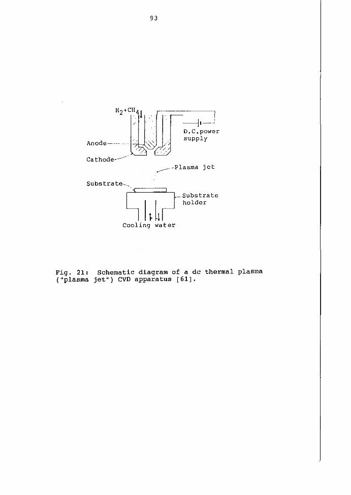
93
H2+C~~41llf__II_~D.C.powersupply
Anode--- - ',v ///, ,//
/
Cathode-------.----- -Plasma jet
SUbstrate-~_~'~======l--
Cooling water
Substrateholder
Fig. 21: Schematic diagram of a dc thermal plasma("plasma jet") CVD apparatus [61].
94
4. CHARACTERISTICS (PROPERTIES) OF DIAMOND AND
DIAMONDLIKE COATINGS
A brief summary of structure and properties of the
diamondlike and diamond coatings is presented here. The relevant
literature for each property which has not been mentioned in the
foregoing text and tables is given only.
Structure and bonding
[88,27,28]The structure of the coatings grown by all the method.
varies between amorphous and the well-crystallized diamond
structure and the bonding is characterized by presence of both
sp3 and sp2 bond types, the percentage of sp2 varying from about
45% in polymerlike coatings, via 30% in hard DLC, to nearly 0%
in diamond layers.
The physical methods (sputtering and ion-beam methods)
have been mostly used to prepare diamondlike coatings, although
the possibility of controlling the deposition parameters to the
highest degree permits to obtain materials with structure and
bonding ranging from diamondlike to pure diamond (pure from both
chemical and bonding standpoints), although with many defects in
the latter.
Using the high energy of the ion beam to bombard the
deposited film, the diamondlike character of the latter is
increased both by confering to surface atoms extra kinetic
energy to move into sp3-bonded sites, and removing selectively
by sputtering amorphous or sp2-bonded domains [4].
The DL films are predominantly amorphous, but can have
extensive sp3-bonded short-range order [64,4].
Polycrystalline diamond with crystals up to 5 ~m have also
been obtained.
In the films grown by conventional CVD method without
atomic H (under the conditions suitable for epitaxial growth)
the films had essentially diamond structure, i.e. structure of
the substrate. However, since the used CVD conditions had to
95
differ (for practical reasons) from those ideally suited for
epitaxy, a graphitic component was codeposited, and
subsequentlly removed (in a separate procedure). The bonding
in the final films was sp3 possibly with a small portion of
sp2 bonds.
In the method using atomic hydrogen, it removed
selectively the sp2 bonds during the deposition, so that
the resulting diamond was virtually free from sp2 bonds.
In the hot filament method, the working conditions
(high substrate temperature, presence of atomic hydrogen, low
hydrocarbon concentration) are suitable for diamond formation.
The bonding is sp3 with little or none sp2 bonds present, and
the structure is that of diamond.In the plasma CVD methods both diamondlike and diamond
coatings were produced.
The diamondlike coatings cover a rather wide interval of
properties, presumably related to their structure. The
polymerlike films produced with low energy of the ions can not
be regarded as diamondlike because of their properties caused
by their structure. They contain about 50 at% H and larger units
of the starting hydrocarbons can be incorporated into their
structure. In addition, their sp2-hybridized-carbon content
is about 45%.
The hard DL films, unlike the polymerlike ones, do not
depend on the nature of the starting gas because this is
decomposed in the plasma almost down to single atoms [59].
However, similar to polymerlike coatings, they contain large
amount of hydrogen, one part of which is bonded to C-atoms.
The suggested models of the structure of amorphous
materials can be divided in two basic groups - microcrystalline
models and models of a random network [105]. The latter group,
according to which the random character of the network is a
result of a statistical distribution of angles between bonds,
is more widely accepted.
With increasing energy of the ions in the plasma
bombarding the substrate, the amorphous structure is changed
into a quasi-amorphous with crystallites which are of the order
of 0.5 nm [44]. The coatings incorporating larger crystal
96
domains are also often formed.The other end of the interval, diamond coatings, have a
structure varying from amorphous to polycrystalline with defined
crystals up to 10 ~m in size. In addition to crystals containing
detectable graphitic component, apparently "pure" diamond
coatings have been reported in a number of papers.
Microstructure
In general, diamondlike coatings show microstructure
without particular characteristics. The layers are compact,
without visible cracks, pores and do not have a pronounced
surface roughness.
The diamond layers with crystallite dimensions on the
order of microns have a more pronounced surface roughness.
The layers with small crystallites can be smoother.
The ion-beam prepared diamond layers are unusually smooth
and are featureless under SEM.
Density and porosity
[114,124,9,30]
Density of the sputtered DL films is in the range
2.1 - 2.2 g/cm3 •
Density of the ion-beam prepared diamondlike films
depends on hydrogen content and is typically 2.4 g/cm3 for
pure carbon and 1.8 g/cm3 for hydrogen-containing films.
The soft, polymerlike films prepared by RF plasma method
have low density (typically 1.3 g/cm3 ) . The hard films prepared
by RF plasma are characterized by higher density (typically
1.9-2.12 g/cm3). Since these films contain both sp3 and sp2
bonds, their properties (including density) might be expected to
be between those of graphitic carbon and diamond. The relatively
low density values even compared to graphite (2.26 g/cm3 ) are
because of the relatively high hydrogen content and disordered
structure.
97
The linear relationship between density of RF plasma
coatings and the parameter v B/pl/ 2 (determining energy of the
ions impinging on the substrate, see 3.2.2) has been found [18]
for density range between 1.5 and 1.8 g/cm3. In a new review
article [59], a non-linear dependence has been reported to existbetveen density and VB (pressure P being constant) for a density
range between 1.5 and 2.0.
The OLC films produced by dc magnetron sputtering from Ar
C2H2 mixture had a wide density range, from 0.98 to 1.6 g/cm3.
The papers describing diamond coatings preparation usually
do not report density values, but on the basis of other
characteristics it can be concluded that these should be close
to the diamond density (3.5 g/cm3) at least for well defined
crystalline layers.
Porosity of the OL coatings is very small and sometimes
layers 1 ~m thick are obtained which show no porosity at all;
they are also pinhole-free. Such properties are precondition for
protective coatings.
Mechanical properties
[114,124,7,83]
Adhesion of the DL coatings (produced by RF plasma) is
strong to diamond or carbide forming substrates, which is
explained by an interfacial carbide layer formation. Adherence
is less on other materials. Adherence of diamond layers produced
by RF or MW plasma is generally very good and even excellent.
Stress in the coatings is generally reported to exist.
Low-thickness films do not exhibit stress, but thicker OL films
tend to separate from the substrate because of the internal
compressive stress, as found for the ion-beam prepared layers.
Diamond layers prepared by MW plasma method showing excellent
adhesion, develop high tensile stress and cause curvature or
even disintegration of the substrate.
Sliding friction was found to be very low for diamondlike
coatings prepared by RF plasma method. Sliding friction
coefficient values were found to increase with relative humidity
from 0.01 to 0.3. In vacuum or very dry nitrogen it is 0.02, but
98
increase in relative humidity from 10 to 99% leads to an
increase of friction coefficient from 0.05 to 0.3.
Microhardness of polymeric coatings obtained by RF plasma
method is low (4 on the Mohs scale). DL coatings obtained by dc
plasma have microhardness up to 30 GPa, and those prepared by RF
plasma (according to different authors) 7-8 (Mohs) or 30-46 GPa.
Diamond coatings obtained by conventional CVD, RF plasma,
MW plasma and thermal plasma methods have similar hardness.
The values reported are mostly in the range from 70 to 120 GPa,
i.e. virtually identical to natural diamond hardness, although
lower values (35 GPa) have also been found.
Electrical properties
The electrical resistivity values reported for diamond
coatings prepared by different methods (ion beam, CVD,
dc plasma, RF plasma, MW plasma are within 1_1015 ohm cm range.
The diamondlike coatings obtained by ion beam methods have
resistivity in the 10 11_10 12 range, but a wide range, extending
from 10 7 to 10 16 ohm cm was found for hydrogen-containing DLC.
Electrical resistivity of diamondlike coatings prepared by
dc plasma is 10 10_10 12 ohm cm. This interval can be extended
(10 3_10 15) varying the deposition temperature, the higher the
deposition rate, the lower the electrical resistivity.
A very broad range of electrical resistivity values
(from 1 ohm cm to 10 14 ohm cm was found for RF plasma deposited
coatings, but values in the range 10 9_10 12 ohm cm seem to be
most frequently reported. Dependence on deposition rate, i.e. on
the discharge power, has been found, the lower the power (and,
consequently, the lower the deposition rate), the higher the
resistivity; however, different resistivity intervals were found
by different researchers for similar power or deposition rate.
The substrate temperature (Td) was found to have a
pronounced effect on electrical resistivity, the latter
decreasing rapidly with increasing Td. A decrease in resistivity
from 1011 to 10 3 was produced by temperature increase of only
500C (from 250 to 300 oC). This effect, as well as the effect of
99
substrate potential on resistivity (resistivity decreases with
VB) is related to hydrogen content which decreases with
increasing VB and Td'The hydrocarbon gas (CH4, C2H6' C2H2 or C2H4) influences
the resistivity, which differs up to a factor of about 3 for the
coatings prepared from methane and ethylene at Td=250oC
(resistivity (methane)/ resistivity (ethylene) > 10 3).
Good insulating properties of the coatings are ascribed to
saturation of dangling bonds by hydrogen.
For very thin films « 50 nm) electrical resistivity wasfound to increase exponentially with decreasing film thickness.
This effect is due to the fact that thinner films are closer to
the ideal amorphous state.
Doping of the coatings with elements of group III and V of
the periodic system was effected using B2H6 (for B) and PH3(for Pl. Doping with N, Ta and Ru has also been reported.
Breakdown strength of diamond like films obtained by ion
beam and RF plasma methods has a value ~106 V/cm.
Dielectric constant for DL films obtained by ion-beam
method is 8 and for diamond films obtained by CVD method is 4-6
(compared to 5.8 for natural diamond).
Optical properties
[75,99]
Index of refraction (n) of polymer1ike films is 1.6-1.65,
but for DLC it was found to vary in a broad range (1.8-2.8)
although majority of papers report values in the range 1.8-2-3.
A linear relation was found between nand VB/P (for the range
1.8-2.15), the slope of the straight line being changed at
n=2.05.
The n values found for diamond layers are 2.38 if
obtained by CVD and 2.36-2.73 when obtained by microwave
plasma (the n value of the natural diamond is about 2.40).
Optical gap (Eg) of DL films amounts to 3.0 eV for
polymerlike films, 0.40-0.74 eV for the DL films prepared by
sputtering in Ar atmosphere. Eg=1.2 eV was found for the films
obtained by ion beam sputtering (in vacuum). The DL films
100
obtained by dc plasma and RF plasma have Eg values in the range
from 0.8 to 1.8 eV, although most often reported values are from
0.8 to 1.1 eV. The Eg is reported to increase with hydrogen
content of the film, and to decrease with deposition
temperature, especially above 250°C.
Transparency of the polymerlike films is good in the
visible and IR (high Eg values). Transparency of the DL films is
generally good in the IR; thin DL films are transparent also in
the visible.
For the diamond coatings, transparency in the visible part
of spectrum depends on the presence of non-diamond (graphitic)
phases, the less the sp2 bonding, the higher transparency. The
diamond coatings, prepared by CVD were found to be transparent
even in UV (wavelengths above 225 urn), similar to natural
diamond.
minimumis generally very good.
range is 85-93%, showing a
Transparency in the IR
Transparency in the 2.5-25 ~m
(68%) at 13.3 ~m.
Absorption of DL films in IR (and in the red part of the
visible spectrum) is very low, both for ion beam and RF plasma
prepared films, becoming almost zero for wavelengths above
1.5 ~m. The adsorption is low for both hydrogen-containing and
no-hydrogen films prepared by the ion beam method.
Absorption of diamond films prepared by MW plasma is low
in the IR, but absorption coefficient increases with decreasing
wavelength.
Thermal properties
Room temperature thermal conductivity values for ion beam
prepared DLC greater than 700 W/mK have been measured [4] (for
comparison, room temperature thermal conductivity of natural
diamond, the highest of all known materials, is about 2000
W/mK).
101
Chemical properties
Diamondlike coatings are chemically resistant to most
acids, bases and solvents [4].Diamond layers are stable even to the most aggressive
chemical agents (HN03+H2S04 (1:3), H2S04+K2Cr207' aqua regia,
concentrated HF).
102
5. APPLICATIONS
The major useful properties of the diamond and diamondlike
films include the following. i) transparency; ii) electrical
insulation; iii) high breakdown voltage; iv) high thermal
conductivity; v) chemical resistance to most acids, bases and
solvents; vi) barrier properties; vii) hardness; viii) good
adhesion to many substrates; ix) wear resistance; x) low
coefficient of friction; xi) deposition on substrates at
slightly above room temperature. The ion beam methods of DLe
preparation can provide, in addition, remarkably smooth films.
The methods of the diamond coating preparation developed
up to the present permit preparation of monocrystalline and
polycrystalline coatings. The monocrystalline films can be
produced at a slow rate (of the order of 1 ~m/h), while
polycrystalline coatings have been prepared at various rates
ranging from .several tenths of ~m/h up to hundreds ~m/h.
Properties of diamond coatings are much closer to those of
natural diamond than are properties of diamondlike coatings and
therefore field of their potential application is very broad.
Most of applications of diamond and diamondlike coatings
can be grouped under the categories of optical, electrical,
thermal, chemical and mechanical. Fig. 22 shows possible
application of the diamond films in relation to their properties
[105] and gives an idea of applications of both diamond and
diamond like coatings. The following text contains more data.
Optical
An initial application for the transparent diamondlike
coatings was as protective coatings for plastic lenses. The
hardness of the coatings, good adhesion to plastics, high
transmission in the visible (water-clear to slightly yellow in
colour), and the low deposition temperature made this attractive
application. The experiments performed indicated that
diamondlike coatings could indeed improve scratch resistance
of these lenses [99].
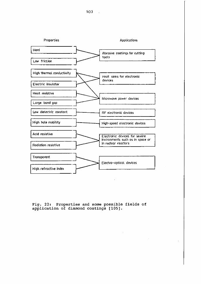
103
Properties Applications
Hard
Low triet Ion
Hleh thermal conductivity
Eloctrlc Insulator
IHoot rostsuvc
I l.orqe bond 90P
Abrasive coatings tor cuttinqtools
Heat sinks tor electronicdevices
Microwovo power devices
RF electronic devices
HI9h bote mobility
I Low dielectric constant Jr-----:===========~r------J Hi<;Jh-spccd electronic devices
'------------'
IAdd resistive
IRadiation resistive
ITransparent
IHi9h refractive index
Electronic devices for severeinvironments such as in spoce orIn rocteor roactors
Eleetro- opticct devices
Fig. 22: Properties and some possible fields ofapplication of diamond coatings [105].
104
A low coefficient of absorption in the IR makes
diamondlike films very promising as antireflecting, and also
erosion-and corrosion-resistant coatings for IR optics.
Furthermore, the index of refraction of diamondlike coatings
can be varied in the range 1.8-2.1 by changing deposition
parameters, e.g. under the RF plasma conditions. This allows
production of single-layer antireflection coatings for optical
materials which have refraction indices in the range of about
3.24-4.41. Very important materials for IR techniques are Ge,
Si and GaAs with n values of 4.0, 3.4 and 3.34, respectively.
One of the most important applications of the diamondlike
films are as coatings for germanium IR optical elements. Owing
to the possibility of making its refractive index n equal to 2,
diarnondlike film is an ideal antireflection as well as
protective coating for Ge with refractive index of 4 [17].
It has been shown that it is possible to increase transmission
of IR radiation (at 5 ~m wavelenth) from 49% for uncoated
Ge windows to 96% for windows coated by diamondlike films of
proper thickness on both sides (Fig. 23) [48,47].
Diamondlike coatings can be used to reduce reflection
losses of Si solar cells. The effect of enhanced infrared
transmission for Si wafer coated with a thin diamondlike film
is illustrated in Fig. 24. The high hardness of the diamondlike
films also imparts abrasion protection to these infrared optical
materials.
The use of ion beam diamondlike films as protective
coatings for optical elements in high power lasers was suggested
for a number of reasons. Included were adhesive strength of the
coating to optical materials such as glass and CaF2' low optical
absorption throughout the visible and infrared spectral regions,
expected abrasion protection, and the capability to form a
hermetic coating with chemical resistance to acids, bases and
solvents [4].
Plasma formation at the surface of mirrors and windows
inside the laser cavity also causes problems in high power
lasers. Small defects on the surface of laser optics can be the
initiation sites for the breakdown plasma, which then degrades
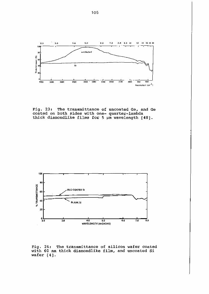
105
a.s a.e ... s.o , .o 7.' , .e s.c W ra " 16 lli 20
eo a..f::{Cc/a-C
"S"60,-..j',,.~
o«oc asoo coco ace "'" . '"'" '000 "'" J~OO ".,. ~ '00
....~\"rnr.b.'r (=_1)
Fig. 23: The transmittance of uncoated Ge, and Gecoated on both sides with one- quarter-lambdathick diamondlike films for 5 ~m wavelength [48].
./DLe-COATED SI
'00
80wuz
E60
•~z• 40">-~
20
02,5 3,0
BLANKSI
4.0 5.0WAVELENGTH (MICRONS)
6,0 7,0 B,O
Fig. 24: The transmittance of silicon wafer coatedwith 60 nm thick diamondlike film, and uncoated Siwafer [4].
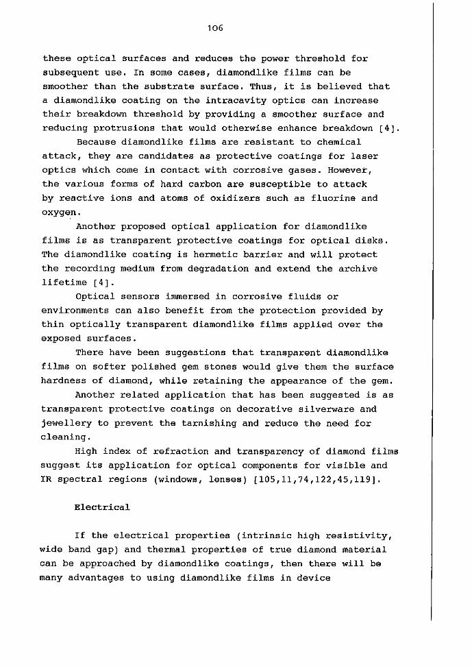
106
these optical surfaces and reduces the power threshold for
subsequent use. In some cases, diamondlike films can be
smoother than the substrate surface. Thus, it is believed that
a diamondlike coating on the intracavity optics can increase
their breakdown threshold by providing a smoother surface and
reducing protrusions that would otherwise enhance breakdown [4].
Because diamondlike films are resistant to chemical
attack, they are candidates as protective coatings for laser
optics which corne in contact with corrosive gases. However,
the various forms of hard carbon are susceptible to attack
by reactive ions and atoms of oxidizers such as fluorine and
oxygen.
Another proposed optical application for diamondlike
films is as transparent protective coatings for optical disks.
The diamondlike coating is hermetic barrier and will protect
the recording medium from degradation and extend the archive
lifetime [4].
Optical sensors immersed in corrosive fluids or
environments can also benefit from the protection provided by
thin optically transparent diamondlike films applied over the
exposed surfaces.
There have been suggestions that transparent diamondlike
films on softer polished gem stones would give them the surface
hardness of diamond, while retaining the appearance of the gem.
Another related application that has been suggested is as
transparent protective coatings on decorative silverware and
jewellery to prevent the tarnishing and reduce the need for
cleaning.
High index of refraction and transparency of diamond films
suggest its application for optical components for visible and
IR spectral regions (windows, lenses) [105,11,74,122,45,119].
Electrical
If the electrical properties (intrinsic high resistivity,
wide band gap) and thermal properties of true diamond material
can be approached by diamondlike coatings, then there will be
many advantages to using diamondlike films in device
107
applications. Diamondlike films with high resistivity,
>10 11 ohm cm, have already been deposited. Ion beam deposited
diamondlike films can exhibit a thermal conductivity greater
than 700 W/mK [4]. This combination of high thermal conductivity
and high electrical resistivity makes diamondlike films
attractive as a dielectric layer for high temperature devices.
However, diamondlike films with a band gap greater than about
2 eV have not yet been demonstrated [4].
As an example of the use of ion beam deposited diamondlike
films in electronic device applications, thin film silicon field
effect transistors (FET) with insulating diamondlike films were
fabricated (Fig. 25).
Possibility of application of diamond coatings for
electronic devices is pointed out by a number of authors
[45,84,56,23,74,106,105]. Radiation hardened semiconductor
devices, high-temperature electronics, high-density, high-speed
integrated circuits, UV-light emitting diodes and lasers have
been mentioned [106].
Among the possibilities of application of diamond
coatings, their doping leading to production of p- and n-type
semiconductor layers has been mentioned [105,92].
It is expected that diamondlike films will play a special
role in applications where the power density is high. An example
of this will be found in the next generation of high density
integrated circuits. These devices will permit shorter signal
transit distances and reduce communication time between
transistors and memory cells, resulting, in higher computation
rates. Because of the ability of the resulting devices to
operate at higher temperatures, cooling requirements can be
reduced and the operating lifetime can be much greater.
This will be important in the new supercomputers where the
high power density currently makes sophisticated cooling
systems a requirement [4].
Another important application can be for semiconductor
circuits used in space enviroments. Here, the high temperature
capability will permit lighter cooling systems to be used.
Also, the radiation resistance of diamondlike devices will
permit a reduction in the weight of radiation shields.
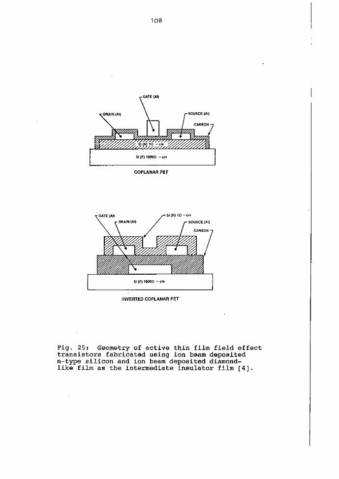
108
COPLANAR FET
QA.TE {AI)
Si (P) 10000 - em
INVERTED COPLANAR FET
Fig. 25: Geometry of active thin film field effecttransistors fabricated using ion beam depositedn-type silicon and ion beam deposited diamond-like film as the intermediate insulator film [4].
109
Both of these features can permit the weight and cost of
satellites to be reduced, and increase operating life.
This radiation resistance property will also be important
for a variety of military applications and nuclear power
plant electronics.
Thermal
The power dissipation of a solid state device such as a
microwave oscillator or power transistor can be significantly
increased if it is mounted on a substrate (such as copper) that
permits thermal energy to be efficiently transferred away from
the device.If the device must be electrically isolated from the
cooling substrate, it is desirable to use an insulating layer
with high breakdown voltage (so that it can be made thin) and
high thermal conductivity.
Because diamondlike films (i) can exhibit high thermal
conductivity, (ii) can be made thin while providing the
necessary electrical isolation, and (iii) do not require
intermediate bonding layers (which may cause phonon impendance
mismatch) to adhere to most substrates, they should find use as
insulating layers in many high power or high density device
applications.
Provided that diamondlike films can be made thick enough,
they may find use as heat spreaders. However, because of the
thickness required (usually >100 ~m) this application will
probably be better fulfilled by polycrystalline diamond films.
High thermal conductivity of diamond coatings in
combination with high electrical resistivity, good heat
resistance and large band gap open possibilities of their
application as heat sinks in various electrical components
[105,74,106,119).
110
Chemical
The chemical resistance to most acids, bases and solvent
permits the use of diamondlike films as protective coatings for
various applications.
The inert nature of diamondlike films suggested its use
as a blood compatible coating for use in the artificial heart
program. Additionally, use of diamondlike films as tissue
compatible coatings for other artificial organs or biological
implants such as hip joints and plastic replacement arteries
or veins used in bypass operations has been suggested [4].
The roles of in-vivo protective coatings are (i) to be
biologically inert to blood contact, (ii) to prevent harmful
components (e.g. plasticizers, monomers, filters) of the
artificial organs from leeching into the blood, and (iii) to
prevent blood components from leeching into the plastic to
degrade the performance and lifetime. Because the chemical
composition is similar to organic material, and since the dense
lattice provides an excellent diffusion barrier, diamondlike
films were considered nearly ideal coatings.
It was also expected that the smooth surface and inert
nature of diamondlike films would hinder the formation of blood
clots. unfortunately, it was found that when plastic substrates
had surface structural defects or inclusions larger than 100 nm,
a diamondlike coatings of about 100 nm thickness could not cover
these defects, and blood clots would eventually form.
This result suggested that thicker protective coatings
and/or much smoother test substrates were required. At the time
of the tests, plastic substrates without defects could not
always be supplied. If artificial hearts made of plastics are to
be practical in the long term, then plastic surfaces without
clot nucleating defects are needed, even if the plastic material
and diamondlike coating are intrinsically blood compatible [4].
Diamondlike coatings have been shown to be an effective
hermetic seal (moisture barrier), capable of extending the lifeof optical fibers.
111
An ion beam coating system was designed and built to
permit in-line deposition of diamondlike films onto an optical
fiber after it was drawn, but prior to application of the
protective polymer coating. With this system, diamondlike
coatings up to a thickness of about 30 nm were applied.
The films could not be made thicker because of the limited
discharge power and cooling capability in the coating section,
and because the fiber could not be drawn too slowly.
This 30 nm diamondlike coating improved the fiber
strength as determined by measurements of the breaking strength
as a function of strain rate (dynamic fatigue). These data
permitted calculation of parameters that predicted an
improvement in strength under constant strain (static fatigue)
relative to the case where only polymer coatings were used [4].
The insulating protective diamondlike coating has
advantages over metallic coatings when interferences due to
electromagnetic pulses occur.
Because of their quasi-amorphous structure, diamondlike
films are almost without pores of sizes which would be large
enough to allow passage of corrosion-active gases and liquids.
A diamondlike coating 0.1 ~m thick noticeably reduced
permeability to the ions of an electrolyte solution and with
1 ~m thick coating the protective action is greatest and hardly
changes at greater thickness. Various authors [7,123] have
reported complete stability of diamondlike films tenths to a few
~m thick to strong acids, alkalies and organic solvents, as well
as their ability to protect a number of materials (AI, Si,
glass, etc). against corrosion-active agents.
A 60 nrn thick diamondlike coating has been shown to be an
efficient barrier against water vapour penetration into the
surface layer of fused quartz, so that preservation of strength
of fibre optics elements can be ensured for a long time [102].
A similar example of protection of the output window of a
semicondu~tor laser against degradation caused·by atmospheric
moisture and oxygen has been reported. The service life of the
protected laser device amounted to about 6000 h [105].
112
Applications of diamond coatings for electronic devices
(as in space or nuclear reactors), based on their chemical and
radiation resistance, have been mentioned [106,105].
Mechanical
Because of the hardness, smoothness and low friction
coefficient od diamondlike coatings, it was anticipated that
these films on the edges of cutting and razor blades would
improve performance.
Experimental results showed that diamondlike coatings on
industrial cutting blades reduced the cutting force required to
slit paper by more than a factor of four, presumably by reducing
friction between the paper and the blade. Second, the coated
blades could cut about 100 times longer than the uncoated blades
before the same cutting force was reached. It is anticipated
that diamondlike films on other cutting tools (e.g. knives,
scalpels, microtomes) can improve their cutting abilities, and
extend the period of sharpness under use [4].
Diamondlike coatings on certain machine tools used under
high force or load may also provide some degree of protection.
However, if high temperatures occur at the cutting edge, the
diamondlikefilms will be rapidly degraded by oxidation. Also,
diamondlike films begin to decompose by losing hydrogen at about
400°C. The diamondlike coatings are probably not appropriate for
application on tool bits for machining iron or steel, because
chemical reaction between the carbon film and iron will occur.
Machining non-ferrous materials and ceramics is a possibility.
Another important application of diamondlike coatings will
be for wear protection of magnetic recording disks and thin film
media. An example is a procedure in which a 40 nm diamondlike
film was used to protect a Zn-Mn ferrite head against wear for
a long-term operation, and which could be applied to all types
of magnetic heads for video recording units [123].
Diamondlike coatings have already demonstrated the ability
to protect Winchester disks from head crashes. The diamondlike
coating also protects the disk against chemical reaction with
113
lubricating fluids. There will be many other wear-related
applications (e.g. ball bearings, bearing races, valves, seals,
etc.) which can benefit from the application of a smooth, low
friction diamondlike coating.
The rigidity of diamondlike films has resulted in a novel
application associated with loudspeakers. Because of the
stiffness of the diamondlike film relative to the added mass,
the response of coated titanium tweeters in the high frequency
range (20-35 kHz) is significantly improved compared to that of
uncoated tweeter [4].
The obvious possibilities of using diamond films as hard,
wear resistant coatings for cutting tools and other applications
have been mentioned [84,74,105].
114
6. CONCLUSION
The investigations lasting for several decades in which
many researchers allover the world have been involved have
established working conditions for fabrication of carbon
coatings having various properties ranging from low-density,
soft, high hydrogen content, polymerlike, to denser, hard
coatings with less hydrogen.
The latter, diamondlike coatings can be produced by a variety
of physical and chemical methods, but RF plasma CVD methods
have been mostly used. The apparatus (standard, commercial
RF systems), experimental conditions used (low pressure plasma,
variety of substrates held at ambient temperature or close to
it, variety of hydrocarbons mixed with Ar or He) and attractive
properties of DLC (transparency, high electrical resistivity,
high breakdown voltage, high thermal conductivity, chemical
resistance, hardness, adhesion to many substrates, wear
resistance), have made them attractive for many applications.
The diamondlike coatings can be also produced by other
plasma CVD methods (dc or MW plasma). Common to all chemical
methods used for diamond like coatings preparation are low
substrate temperature, high hydrocarbon gas concentration
(up to 100%) and no hydrogen in the initial gas mixture.
Physical methods (sputtering and ion beam) have been
used too. The ion beam methods in particular, permitting
greater control of deposition parameters than any other method,
can be used to produce deposits with desired composition and
properties. The deposits obtained are generally similar to those
prepared by other methods, but certain important differences
exist, e.g. their exceptional smoothness.
The diamond coatings have first been produced already
3.5 decades ago but interest of researchers was stimulated only
much later when they have been produced by plasma CVD methods.
Today diamond coatings can be produced by a number of
methods.
The plasma CVD methods use dc, RF or MW commercial
apparatus. Working conditions used for diamond coating
115
preparation .common to all these methods are a low concentration
of hydrocarbon in hydrogen, high ionization efficiency of the
plasma providing suitable species for diamond formation, in
particular high concentration of atomic hydrogen, substrate
temperature most often in the range 700-l000°C; it is desirable,
but apparently not indispensable to have a substrate surface
suitable to promote diamond nucleation (containing diamond seed
particles, or consisting of diamond, a diamond-lattice-matching
carbide or carbide-forming metal).
A simplified picture of the processes leading to diamond
coating formation would be as follows.
The role of the plasma is to decompose and ionise
hydrocarbon and to form atomic hydrogen in superequilibrium
concentration (with respect to substrate temperature). The ions
and fragments consisting mainly of carbon are deposited on the
substrate, the temperature of which ensures the surface
mobility. The atomic hydrogen preferentially reacts with
sp2 bonded atoms and removes them, leaving and stabilizing
sp3 bonded C atoms on the surface.
Nucleation is favorized by presence of diamond seed
crystals or a carbide with a crystal lattice matching that
of diamond.
The role of the hot filament (~2000°C) placed at an
appropriate distance from the substrate (heated to 700-1000°C)
is essentially the same as the role of plasma. The same is valid
for thermal plasma, in which very high temperature (5000 0C)
leads to both high degree of decomposition of hydrocarbon and
production of atomic hydrogen. The substrate temperature is
again in the same range as in the other methods.
By means of the physical methods, diamond coatings can
be deposited on non-carbon substrates kept at or near room
temperature, using energetic carbon ions, preferably without
accompanying neutral particles.
It is clear therefore that the factors playing essential
role in the chemical deposition methods (high substrate
temperature, presence of atomic hydrogen) do not exist in the
case of physical methods. Their role must therefore be played
116
by the energetic particles, but the mechanisms of their action
are rather poorly understood.
The ion bombardment increases the diamondlike component
by giving surface atoms extra kinetic energy to move into sp3
bonded sites, and by preferential removal by sputtering of
amorphous or sp2 bonded domains. According to a recent
"s ubplantation model" for mass-selected ion beam deposition,
a dense sp3 matrix evolves from hyperthermal carbon ion
impingement due to preferential displacement of sp2 bonded atoms
and due to the "mold" effect of the host matrix which imposes
the structure to be formed. According to the model, the optimum
energy range for the diamond evolution is about 60-180 eV, and
substrate temperature ~70°C. Higher substrate temperature
(~100°C) would lead to evolution of graphitic films due to
C-substrate diffusion and ion mixing.
With structure varying from amorphous to polycrystallyne
with crystals up to 10 ~m, the reported properties of diamond
coatings also vary, but can be made close to those of natural
diamond.
The existing applications of diamondlike coatings are
already numerous (antireflecting/protective coatings for optical
elements, Ge in particular, coating of cutting tools to increase
their performance, wear protection of magnetic recording
elements, coatings on loudspeakers to improve their response,
insulating coatings on silicon field-effect transistors).
Many other applications are possible, although some of
them require certain improvements in diamondlike
characteristics.
Prospects for a wide application of diamond coatings seem
real. Certain characteristics of diamond coatings are better
than those of diamondlike coatings (higher thermal conductivity,
higher heat and chemical resistance) and can be therefore more
suitable for certain applications (e.g. in high power devices,
for machine tools used under high force or load and thereby
heated up to high temperatures, for better corrosion protection
etc.) .
117
However, diamond coatings can not replace diamondlike
coatings in all applications. Properties of diamondlike coatings
are different from those of diamond, but also can be varied
in a certain range to make them optimum for a given application
(e.g. refractive index can be made 1.84 or 2.0, which are
optimum values for antireflecting coatings on Si and Ge,
respectiveLyj .
Thus, both diamond and diamondlike coatings may be
expected to have their applications. Which material will be
chosen for a given application will depend on its
characteristics, but also on the conditions of its preparation
(e.g. high temperature used in the majority of methods of
diamond preparation restricts the choice of substrate
materials), possibility to be produced on sufficiently large
surface area and/or with sufficient uniformity of thickness,
economic and other factors.
118
REFERENCES
1. Aikyo H. and Kondo K., Jpn. J. Appl. Phys., 28 (1989)L1631.
2. Aisenberg S. and Chabot R., J. Appl. Phys., 42 (1971) 2953.
3. Aisenberg S., J. Vac. Sci. Technol., A 2 (1984) 369.
4. Aisenberg S. and Kimock F.M., Mat. Sci. Forum,52 & 53 (1989) 1.
5. Akatsuka F., Hirose Y. and Komaki K., Jpn. J. Appl. Phys.,27 (1988) L1600.
6. Andersson L.P., Berg S., Norstrom H., Olaison R. andTowta S., Thin Solid Films, 63 (1979) 155.
7. Andersson L.P., Thin Solid Films, 86 (1981) 193.
8. Angus J.C., Will H.A. and Stanko W.S., J. Appl.Phys.,39 (1968) 2915.
9. Angus J.C., Stultz J.E., Shiller P.J., MacDonald J.R.,Mirtich M.J. and Domitz S., Thin Solid Films,118 (1984) 311.
10. Anttila. A., Koskinen J., Lappalainen R., Hirvonen J-P.,Stone D. and Paszkiet C., Appl. Phys. Lett., 50 (1987) 132.
11. Badzian A., Simonton B., Badzian T., Messier R. t
Spear K.E. and Roy R., Proc. SPIE, 683 (1986) 127.
12. Badzian A.R., Badzian T., Roy R., Messier R. andSpear K.E., Mat. Res. Bull., 23 (1988) 531.
13. Balakov A.V. and Konshina E.A., Zh. Tekhn. Fiz.,52 (1982) 810.
14. Banks B.A. and Rutledge S.K., J. Vac. Sci. Technol.,21 (1982) 807.
15. Berg S. and Andersson L.P., Thin Solid Films,58 (1979) 117.
16. Bonnot A.M., Thin Solid Films, 185 (1990) 111.
17. Bubenzer A., Dischler B. and Nyaiesh A, Thin Solid Films,91 (1982) 81.
18. Bubenzer A., Dischler B., Brandt G. and Koidl P.,J. Appl. Phys., 54 (1983)4590.
19. Buckley R.G., Moustakas T.O., Ye L. and Varon J.,J. Appl. Phys., 66 (1989) 3595.
20. Bundy F.P., Hall H.T., Strong H.M. and Wentorf R.H.,Jr.,Nature, 4471 (1955) 51.
21. Catherine Y. and Couderc P., Thin Solid Films,144 (1986) 265.
22. Catherine Y., Mat. Sci. Forum, 52 & 53 (1989) 175.
11 9
23. Collins C.B., Davanloo F., Juengerman E.M., Jander D.R.and Lee T.J., Proc. SPIE, 1112 (1989) 192.
24. Cotton F.A. and Wilkinson G., Advanced InorganicChemistry, John Wiley, N.Y., 1980.
25. Couderc P. and Catherine Y., Thin Solid Films,146 (1987) 93.
26. Craig S. and Harding G.L., Thin Solid Films, 97 (1982) 345.27. Derjaguin B.V., Spitsyn B.V., Gorodetsky A.E.,
Zakharov A.P., Bouilov L.L. and Aleksenko A.E.,J. Cryst. Growth, 31 (1975) 44.
28. Derjaguin B.V., Fedoseev D.V., Varnin V.P. andVnukov S.P., Nature, 269 (1977) 398.
29. Dischler B., Bubenzer A. and Koidl P., Solid StateCornrnun., 48 (1983) 105.
30. Dischler B., Bubenzer A. and Koidl P., Appl. Phys. Lett.,42 (1983) 636.
31. Ehrhardt H., Kleber R., Scheppat B., Fuchs A.,Dworschak W., Scherer J. and Jung K., in: Broszeit E.,Mlinz W.D., Oechsner H., Rie K-T. and Wolf G.K.,(eds),Plasma Surface Engineering, Vol. 2 (1989) 1113.
32. Enke K., Dimigen H. and Hlibsch H., Appl. Phys. Lett.,36 (1980) 291.
33. Enke K., Thin Solid Films, 80 (1981) 227.
34. Enke K., Mat. Sci. Forum, 52 & 53 (1989) 559.35. Eversole W.G. and Kenmore N.Y., U.S. Patent No 3,030,188,
(1962) .36. Fang R.C. and Ley L., in: Broszeit E., Mlinz W.D.,
Oechsner H., Rie K-T. and Wolf G.K., (eds),Plasma Surface Engineering, Vol 2 (1989) 1081.
37. Field J.E., (ed), The Properties of Diamond,Academic Press, London, 1979.
38. Fujimori S. and Nagai K., Jpn. J. Appl. Phys.,20 (1981) L194.
39. Gambino R.J. and Thompson J.A., Solid State Cornrnun.,34 (1980) 15.
40. Gautherin G. and Weissmantel Chr., Thin Solid Films,50 (1978) 135.
41. Gonzalez-Hernandez J., Asomoza R., Reyes-Mena A.,Rickards J., Chao S.S. and Pawlik D., J. Vac.Sci.Technol., A 6 (1988) 1798.
42. Grischke M., Harnack J.T., Benndorf C. and Thieme F.,in: Broszeit E., Mlinz W.D., Oechsner H., Rie K-T. andWolf G.K. (eds), Plasma Surface Engineering, Vol. 2(1989) 1093.
43. Hai-bou J. and Xin-sheng P., Ibid, p. 279.
44. Hauser J.J., J. Non-Cryst. Solids, 23 (1977) 21.
120
45. Hirose Y. and Terasawa Y., Jpn. J. Appl. Phys.,25 (1986) L519.
46. Holland L. and Ojha S.M., Thin Solid Films, 38 (1976) L17.
47. Holland L. and Ojha S.M., Thin solid Films, 48 (1978) L21.
48. Holland L. and Ojha S.M., Thin Solid Films, 58 (1979) 107.
49. Hsu W.L., Tung D.M., Fuchs E.A., McCarty K.F., Joshi A.and Nimmagadda R., Appl. Phys. Lett., 55 (1989) 2739.
50. Ishikawa J., Takeiri Y., Ogawa K. and Takagi T.,J. Appl. Phys., 61 (1987) 2509.
51. Jansen F., Machonkin M., Kaplan S. and Hark S.,J. Vac. Sci. Technol., A 3 (1985) 605.
52. Jones D.I. and Stewart A.D., Phil. Mag. B, 46 (1982) 423.
53. Kamo M., Sato Y., Matsumoto S. and Setaka N.,J. Cryst. Growth, 62 (1983) 642.
54. Kamo M., Yurimoto H., Sato Y. and Setaka N.,J. Vac. Sci. Tecnol., A 6 (1988) 1818.
55. Kitabatake M. and Wasa K., J. Vac. Sci. Technol.,A 6 (1988) 1793.
56. Kobashi K., Nishimura K., Kawate Y. and Horiuchi T.,J. Vac. Sci. Technol., A 6 (1988) 1816.
57. Kobayashi K. Mutsukura N. and Machi Y., Thin Solid Films,158 (1988) 233.
58. Kobayashi K., Yamamoto K., Mutsukura N. and Machi Y.,Thin Solid Films, 185 (1990) 71.
59. Koidl P., Wild Ch., Dischler B., Wagner J. andRamsteiner M., Mat. Sci. Forum, 52 & 53 (1989) 41.
60. Kung P.J. and Tzeng Y., J. Appl. Phys., 66 (1989) 4676.
61. Kurihara K., Sasaki K., Kawarada M. and Koshino N.,Appl. Phys. Lett., 52 (1988) 437.
62. Liander H., ASEA J., 28 (1955) 97.
63. Liander H. and Lundblad E., Arkiv Kemi, 16 (1960) 1939.
64. Lifshitz Y., Kasi S.R. and Rabalais J.W., Mat. Sci. Forum,52 & 53 (1989) 237.
65. Littmark U., Paulini H.C. and Danailov D.M.,in: Broszeit E., MUnz W.O., Oechsner H" Rie K.-T.and Wolf G.K. (eds), Plasma Surface Engineering,Vol. 2 (1989) 1101.
66. Marinkovic G. and Marinkovic Z.,(with Kotter H. andMeixner Ch.), Boron Nitride Coatings, InternationalBureau, KFA, Jlilich, 1989.
67. Marinkovic Z. and Roy R., Carbon, 14 (1976) 329.
68. Matsumoto S., Sato Y., Tsutsumi M. and Setaka N.,J. Mat. Sci., 17 (1982) 3106.
69. Matsumoto S., J. Mat. Sci. Lett., 4 (1985) 600.
121
70. Matsumoto 0., Toshima H. and Kanzaki Y., Thin Solid Films,128 (1985) 341.
71. Matsumoto S., Hino M. and Kobayashi T.,Appl. Phys Lett., 51 (1987) 737.
72. Matsumoto O. and Katagiri T., Thin Solid Films,146 (1987) 283.
73. Matsumoto S., Hina M., Moriyoshi Y.,Nagashima T. andTsutsumi M., U.S. Patent, 4,767,608 (1988).
74. Meyer D.E., Dillon R.O. and Woollam J.A., J. Vac. Sci.Technol., A 7 (1989) 2325.
75. Meyerson B. and Smith F.W., J. Non-Cryst. Solids,35 & 36 (1980) 435.
76. Mirtich M.J. and Swec D.M., Thin Solid Films,131 (1985) 245.
77. Mirtich M.J., Mat. Sci. Forum, 52 & 53 (1989) 217.
78. Mitsuda Y., Kojima Y., Yoshida T. and Akashi K.,J. Mat. Sci., 22 (1987) 1557.
79. Miyazawa T., Misawa S., Yoshida S. and Gonda S.,J. Appl. Phys., 55 (1984) 188.
80. Moravec T.J., Thin Solid Films, 70 (1980) L9.
81. Moravec T.J. and Orent T.W., J. Vac. Sci. Technol.,18 (1981) 226.
82. Moravec T.J. and Lee J.e., J. Vac. Sci. Technol.,20 (1982) 338.
83. Mori T. and Namba Y., J. Vac. Sci. Technol.,A 1 (1983) 23.
84. Morrison D. and Savage J.A., Proc. SPIE, 1112 (1989) 186.
85. Nakazawa H., Kanazawa Y., Kamo M. and Osumi K.,Thin Solid Films, 151 (1987) 199.
86. Namba Y., Wei J., Mohri T. and Heidarpour E.A.,J. Vac. Sci. Technol., A 7 (1989) 36.
87. Natarajan V., Lamb J.D., Woollam J.A., Liu D.C. andGulino D.A., J. Vac. Sci. Technol., A 3 (1985) 681.
88. Nemanich R.J., Glass J.T., Lucovsky G. and Shroder R.E.,J. Vac. Sci. Technol., A 6 (1988) 1783.
89. Nir D., Kalish R. and Lewin G., Thin Solid Films,117 (1984) 125.
90. Nyaiesh A.R., Kirby R.E., King F.K. and Garwin E.L.,J. Vac. Sci. Technol., A 3 (1985) 610.
91. Ojha S.M. and Holland L., Thin Solid Films, 40 (1977) L31.
92. Okano K., Naruki H., Akiba Y., Kurosu T., Iida M. andHirose Y., Jpn. J. Appl. Phys., 27 (1988) L173.
93. Ong T.P. and Chang R.P.H., Appl. Phys. Lett.,55 (1989) 2063.
122
98.
97.
95.
94.
96.
101.
99.
100.
102.
104.
103.
107.
106.
105.
108.
109.
110.
111.
Pellicori S.F., Peterson C.M. and Henson T.P.,J. Vac. Sci. Technol., A 4 (1986) 2350.
Peng-sholl Xu and Rong-chuan Fang, in: Broszeit E.,Mtinz W.D., Oechsner H., Rie K.-T. and Wolf G.K. (eds),Plasma Surface Engineering, Vol. 2 (1989) 1121.
Robertson J.L., Moss S.C., Lifshitz Y., Kasi S.R.,Rabalais J.W., Lempert G.D. and Rapoport E.,Science, 243 (1989) 1047.
Sathyamoorthy A. and Weisweiler W., Thin Solid Films,87 (1982) 33.
Savvides N. and Window B., J. Vac. Sci. Technol.,A 3 (1985) 2386.
Savvides N., Thin Solid Films, 163 (1988) 13.
Sawabe A. and Inuzuka T., Appl. Phys. Lett.,46 (1985) 146.
Scharff W., Hammer K., Schmidt G., Stenzel 0., Ullmann J.,Vogel M., Frauenheim T. and Weissmantel C.,in: Broszeit E., Mtinz W.o., Oechsner Ho, Rie K.-T.,and WolfG.K., (eds), Plasma Surface Engineering,Vol. 2 (1989) 1065.
Sokolowski M. and Sokolowska A., J. Cryst. Growth,57 (1982) 185.
Spencer E.G., Schmidt P.H., Joy D.C. and Sansalone F.J.,Appl. Phys. Lett., 29 (1976) 118.
Spitsyn B.V., Bouilov L.L. and Derjaguin B.V.,J. Cryst. Growth, 52 (1981) 219.
Spitsyn B.V., Bouilov L.L. and Derjaguin B.V.,Prog. Crystal Growth and Charact., 17 (1988) 79.
Srikanth K., Ashok S., Badzian A., Badzian T. andMessier R., Thin Solid Films, 164 (1988) 187.
Suzuki K., Sawabe A., Yasuda H. and Inuzuka T.,Appl. Phys. Lett., 50 (1987) 728.
Vitkavage D.J., Rudder R.A., Fountain G.G.andMarkunas R.J., J. Vac. Sci. Technol., A 6 (1988) 1812.
Vora H. and Moravec T.J., J. Appl. Phys., 52 (1981) 6151.
Warner J.D., Pouch J.J., Alterovitz S.A., Liu D.C. andLanford W.A., J. Vac. Sci. Technol., A 3 (1985) 900.
Watanabe I. and Sugata K., Jpn. J. Appl. Phys.,27 (1988) 1397.
Watanabe I. and Sugata K., Jpn. J. Appl. Phys.,10 (1988) 1808.
113. Weissmantel C., Reisse G., Erler H.-J., Henny F.,Bewilogua K., Ebersbach U. and Schtirer C.,Thin Solid Films, 63 (1979) 315.
112.
114. Weissmantel C., Schtirer C., Frohlich F., Grau P. andLehmann H., Thin Solid Films, 61 (1979) L5.
123
115. Weissmantel C., Bewilogua K., Dietrich D., Erler H.-J.,Hinneberg H.-Jo, Klose S., Nowick W. and Reissa G.,Thin Solid Films, 72 (1980) 19.
116. Weissmante1 C., J. Vac. Sci. Techno1., 18 (1981) 179.
117. Whitmell D.S. and Williamson R., Thin Solid Films,35 (1976) 255.
118. Woollam J.A., Natarajan V., Lamb J., Khan A.A.,Bu-Abbud G., Mathine D., Rubin D., Dillon R.O.,Banks Bo, Pouch J. t Gulino D.A., Damitz S., Liu D.C.and Ingram D., Thin Solid Films, 119 (1984) 121.
119. Wort C.J.H., Lettington A.H., Smith C. andHetherington A.V., Proc. SPIE, 1112 (1989) 199.
120. Ya1amanchi R.S. and Thutupalli G.K.M., Thin Solid Films,164 (1988) 103.
121. Yamamoto M., Saitoh K. and Fukui M., in: Broszeit E.,Mlinz W.D., Oechsner H., Rie K.-T. and Wolf G.K. (eds),Plasma Surface Engineering, Vol. 2 (1989) 1073.
122. Yarbrough W.A., Rosen N.D., Pi1ione L.R. and Drawl W.R.,Proc. SPIE, 1112 (1989) 176.
123. Zelez J., RCA Review, 43 (1982) 665.
124. Zelez J., J. Vac Sci. Techno1. Al (1983) 305.
125. Zorin E.I., Sukhorukov V.V. and Tetel'baum D.I.,Zh. Tekh. Fiz., 50 (1980) 175.
126. Kawarada H., Mar K.S. and Hiraki A., Jpn. J. Appl. Phys.,26 (1987) L1032.

Scientific Series of the International Bureau
1 Fundamentos do Metodo de Correntes ParasitasD. Stegemann
2 Diamond and Diamondlike CoatingsS. Marinkovic and Z. Marinkovic with S. Krawczynski

ISBN 3-89336-044-1