Design Methodology and Technology Assessment for High-Density ...
158
THÈSE Pour obtenir le grade de DOCTEUR DE L’UNIVERSITÉ GRENOBLE ALPES Spécialité : Nano électronique et nano technologies Arrêté ministériel : 7 août 2006 Présentée par Hossam SARHAN Thèse dirigée par Fabien CLERMIDY préparée au sein du Laboratoire Intégration Silicium des Architectures Numériques dans l'École Doctorale Electronique, Electrotechnique, Automatique et Traitement du Signal (EEATS) Design Methodology and Technology Assessment for High-Density 3D Technologies Thèse soutenue publiquement le « 23 Novembre 2015 », devant le jury composé de : Mme Lorena, ANGHEL Pofesseur, Univ. Grenoble Alpes, TIMA, Président M. Amara, AMARA Pofesseur, ISEP, Rapporteur M. Jacques-Olivier, KLEIN Pofesseur, Univ. Paris Sud, Rapporteur M. Sung Kyu, LIM Pofesseur, Georgia Institute of Technology, Membre M. Fabien, CLERMIDY HDR, CEA-LETI, Directeur de thèse, Membre M. Sebastien, THURIES Ingenieur de recherche, CEA-LETI, Membre
Transcript of Design Methodology and Technology Assessment for High-Density ...
THÈSE
Pour obtenir le grade de
DOCTEUR DE L’UNIVERSITÉ GRENOBLE ALPES
Spécialité : Nano électronique et nano technologies
Arrêté ministériel : 7 août 2006
Présentée par
Hossam SARHAN Thèse dirigée par Fabien CLERMIDY préparée au sein du Laboratoire Intégration Silicium des Architectures Numériques dans l'École Doctorale Electronique, Electrotechnique, Automatique et Traitement du Signal (EEATS)
Design Methodology and Technology Assessment for High-Density 3D Technologies Thèse soutenue publiquement le « 23 Novembre 2015 », devant le jury composé de :
Mme Lorena, ANGHEL Pofesseur, Univ. Grenoble Alpes, TIMA, Président
M. Amara, AMARA Pofesseur, ISEP, Rapporteur
M. Jacques-Olivier, KLEIN Pofesseur, Univ. Paris Sud, Rapporteur
M. Sung Kyu, LIM Pofesseur, Georgia Institute of Technology, Membre
M. Fabien, CLERMIDY HDR, CEA-LETI, Directeur de thèse, Membre M. Sebastien, THURIES Ingenieur de recherche, CEA-LETI, Membre
Doctoral Thesis
Design Methodology and TechnologyAssessment for High-Density 3D
Technologies
Hossam Sarhan
November 2015
Abstract
Scaling limitations of advanced technology nodes are increasing and the BEOL para-
sitics become more dominant. This has led to an increasing interest in 3D technologies
to overcome such limitations and continue the scaling predicted by Moore’s Law. 3D
technologies vary according to the fabrication process which creates a wide spectrum
of technologies including Through-Silicon-VIA (TSV), Copper-to-Copper (CuCu) and
Monolithic (or sequential) 3D (M3D). TSV and CuCu provide 3D contacts of pitch
around 5-10µm while M3D scales down 3D via pitch extremely to 0.11µm. Such high-
density capability of Monolithic 3D technology creates new design paradigms. In this
context, our objective is to propose innovative design methodologies to well utilize M3D
technology and introduce a technology assessment framework to evaluate different M3D
technology parameters from design perspective.
This thesis can be divided into three main contributions. As creating 3D standard
cells becomes achievable thanks to M3D technology, a new 3D standard cell approach
called ‘3D Cell-on-Buffer’ (3DCoB) has been introduced. 3DCoB cells are created by
splitting 2D cells into functioning gates and driving buffers stacked over each other.
The simulation results show gain in timing performances compared to 2D. By applying
an additionally Multi-VDD low-power approach, iso-performance power gain has been
achieved. Afterwards cell-on-cell design approach has been explored where a partitioning
methodology is required to distribute cells between different tiers, i.e. determine which
cell should be placed on which tier. A physical-aware partitioning methodology has been
introduced which improves power-performance-area results compared to state-of-the-art
partitioning techniques. Finally a full high-density 3D technology assessment study is
presented to explore the trade-offs between different 3D technologies, block complexities
and partitioning methodologies.

Acknowledgements
Here I am reaching the end of this journey. This work would not have been accom-
plished without the efforts of many inspiring people. I would like to acknowledge all of
their contributions. Above all, I am indebted to my thesis director Fabien Clermidy and
my thesis supervisors Sebastien Thuries and Olivier Billoint. I have had the honor and
pleasure of working with such smart and inspiring people. Fabien, Sebastien and Olivier
are great mentors from whom I have learned a lot on the personal and technical levels.
They helped me a lot throughout all my work.
Even though a great effort has been put into this thesis, it would not have been with
any value without the approval of a great jury. First of all, I would like to express my
gratitude to Prof. Jacques-Olivier and Prof. Amara Amara for being the reporters and
for their suggestions. I would also like to thank Prof. Sung Kyu Lim and Prof. Lorena
Anghel for accepting to be part of the thesis jury. It was my pleasure to defend and
discuss my thesis work with such technical experts.
During this work, I have worked in collaboration with many researchers from whom
I have had the chance to learn a lot. I would like to especially thank and acknowledge
the effort of Synopsys/Atrenta SpyGlass team; Vladimir Pasca, Claudia Rusu and Ravi
Varadarajan for their intensive support of SpyGlass Physical tool within a common lab
during my PhD.
I would like to acknowledge as well Perrine Batude for her support and contributions
regarding Monolithic 3D Integration Technology process, Maud Vinet for directing the
research effort in 3D Technologies, Meycene Toumi for his support on SpyGlass 3D tool
flow, Bartosz Boguslawski for his collaboration and great effort in the 3D neural cliques
contribution, Fabien Deprat and Alexandre Ayres for their support and contribution in
the process characterization of Monolithic 3D technology, Edith Beigne for taking the
responsibility of coaching us as PhD students and Pascal Vivet for his fruitful discus-
sions and guidance. I would also like to thank Marc Belleville, Denis Dutoit, Gerald
Cibrario, Guillaume Berhault, Frederic Heitzmann, Cristiano Lopes Dos Santos, Ogun
Turkylimaz, Lilia Zaourar, Bilel Belhadj, Simone Bacles-Min, Houcine Oucheikh, David
Coriat, Thiago Rappu Da Rosa, Yassine Fkih, Santhosh Onkaraiah and Natalija Jo-
vanovic with whom I have exchanged many ideas and have had technical discussions. I
really appreciate their contribution which shaped my thesis research substantially.
I feel privileged for the chance to conduct research in such a dynamic and enriching
workplace as CEA where I have met wonderful people. Especially, I would like thank
ii

iii
the members of my laboratory: Olivier Thomas, Bastien, Jerome, Jean-Frederic, Alexan-
der, Yvain, Ivan, Romain, Pierre-Yves, Michel, Yves, Anthony and my friends Ismail,
Vincent, Brahim, Oussama, Florent, Adam, Alex, Soundous, Emilie, Jolie, Melanie,
Sebastien Bernard, Marie-Sophie, Nour, Mai, Alexandra, Julien, Lionel, Gregory for
making the life in CEA even more enjoyable. I would also like to thank Catherine Bour
and Jumana Boussey for being very helpful during my administrative struggles. I also
want to thank the laboratory secretaries Caroline and Armelle for being kind and patient
even with my limited French. I would like to deeply thank Haykel Ben-Jamaa without
whom my path would have never crossed with CEA; as he was the one to invited me to
this PhD position.
My most thanks, appreciation, and gratitude go to my family. First my wife Nesma
who was part of this journey. She has endured my working late so may times and con-
tinuously encouraged me to continue through all the hard times that I have had. My son
Yusuf whom I have been blessed with during my PhD journey and who has made my
life a lot more joyful. My father Hassan, my mother Nawal, my father-in-law Mokhtar
and my brother Mohamed have all been a source of motivation and strength. Without
their constant encouragement, I would not have been able to get this far. I dedicate this
dissertation to each and every one of my family and my friends for their unconditional
love and generous support.
Hossam Sarhan
Contents
Abstract i
Acknowledgements ii
Contents iv
List of Figures viii
List of Tables x
Abbreviations xii
1 Introduction 1
1.1 Context . . . . . . . . . . . . . . . . . . . . . . . . . . . . . . . . . . . . . 1
1.2 Motivation . . . . . . . . . . . . . . . . . . . . . . . . . . . . . . . . . . . 3
1.3 Contributions . . . . . . . . . . . . . . . . . . . . . . . . . . . . . . . . . . 4
1.4 Thesis Organization . . . . . . . . . . . . . . . . . . . . . . . . . . . . . . 5
2 Overview on 3D Technologies and Design Space 7
2.1 Why 3D ICs? . . . . . . . . . . . . . . . . . . . . . . . . . . . . . . . . . . 7
2.2 3D Design Space . . . . . . . . . . . . . . . . . . . . . . . . . . . . . . . . 8
2.3 3D Technology Spectrum . . . . . . . . . . . . . . . . . . . . . . . . . . . 8
2.3.1 Integration Schemes . . . . . . . . . . . . . . . . . . . . . . . . . . 9
2.3.1.1 2.5D Interposer . . . . . . . . . . . . . . . . . . . . . . . 9
2.3.1.2 3D Configurations: Face-to-Back and Face-to-Face . . . . 10
2.3.2 3D Through-Silicon-VIA Technology . . . . . . . . . . . . . . . . . 11
2.3.3 3D Copper-to-Copper Technology . . . . . . . . . . . . . . . . . . 11
2.3.4 Monolithic 3D (3DVLSI) Technology . . . . . . . . . . . . . . . . . 13
2.3.5 Summary: Comparing different 3D technologies . . . . . . . . . . . 13
2.4 Partitioning Granularity: Stacking from ‘Coarse-grain’ to ‘Fine-grain’ . . 14
2.4.1 Memory-on-logic integration . . . . . . . . . . . . . . . . . . . . . . 15
2.4.2 Core-level and block-level integration . . . . . . . . . . . . . . . . . 16
2.4.3 Gate-level integration (Cell-on-Cell) . . . . . . . . . . . . . . . . . 17
2.4.4 Transistor-level integration (N/P) . . . . . . . . . . . . . . . . . . 17
2.4.5 Logic-on-Logic stacking: Fine vs. Coarse grain Partitioning . . . . 18
2.4.5.1 Coarse-Grain: Architecture-level Partitioning . . . . . . . 18
2.4.5.2 Fine-Grain: Gate-level Partitioning . . . . . . . . . . . . 19
iv
Contents v
2.4.6 Summary: 3D partitioning granularity spectrum . . . . . . . . . . 21
2.5 3D CAD Tools: Issues and Perspectives . . . . . . . . . . . . . . . . . . . 23
2.5.1 Issues of CAD tools for 3DICs . . . . . . . . . . . . . . . . . . . . 23
2.5.1.1 3D Standard Cell Placement . . . . . . . . . . . . . . . . 23
2.5.1.2 3D-VIA Placement . . . . . . . . . . . . . . . . . . . . . . 24
2.5.1.3 3D Clock Tree Synthesis . . . . . . . . . . . . . . . . . . 24
2.5.2 3D Implementation based on 2D Commercial Tools . . . . . . . . . 26
2.5.3 Using Fast Prototyping Implementation Tool . . . . . . . . . . . . 26
2.6 Conclusion: Work positioning and Design Framework . . . . . . . . . . . . 28
3 Cell-on-Buffer: A New Design Approach for Monolithic 3D 30
3.1 Introduction . . . . . . . . . . . . . . . . . . . . . . . . . . . . . . . . . . . 30
3.2 3D Cell-on-Buffer (3DCoB) Approach . . . . . . . . . . . . . . . . . . . . 32
3.2.1 3DCoB cell structure . . . . . . . . . . . . . . . . . . . . . . . . . . 32
3.2.2 3DCoB input gate capacitance . . . . . . . . . . . . . . . . . . . . 33
3.2.3 Results of input gate capacitance effect . . . . . . . . . . . . . . . 34
3.3 3DCoB Implementation Framework . . . . . . . . . . . . . . . . . . . . . . 34
3.3.1 .LEF file generation . . . . . . . . . . . . . . . . . . . . . . . . . . 36
3.3.2 .LIB file generation . . . . . . . . . . . . . . . . . . . . . . . . . . . 37
3.3.2.1 Validating .LIB generation methodology . . . . . . . . . . 38
3.4 3DCoB Performance-Power Results . . . . . . . . . . . . . . . . . . . . . . 40
3.5 Low-Power Multi-VDD CoB (MV-CoB) Approach . . . . . . . . . . . . . 44
3.6 Power Optimization Results MV-CoB Performance-Power-Area Results . 46
3.7 Summary and Conclusion . . . . . . . . . . . . . . . . . . . . . . . . . . . 48
4 Gate-Level 3D Partitioning 51
4.1 Introduction: 3D Partitioning . . . . . . . . . . . . . . . . . . . . . . . . . 51
4.2 Previous Gate-Level Partitioning Techniques . . . . . . . . . . . . . . . . 53
4.3 Physical-Aware Partitioning (PAP) Methodology . . . . . . . . . . . . . . 54
4.4 Bi-Directional Partitioning (BDP) Algorithm . . . . . . . . . . . . . . . . 57
4.5 Un-Balancing Area Ratio Concept . . . . . . . . . . . . . . . . . . . . . . 60
4.6 Performance-Power-Area Results . . . . . . . . . . . . . . . . . . . . . . . 62
4.6.1 PAP Methodology Implementation . . . . . . . . . . . . . . . . . . 62
4.6.2 Performance Results . . . . . . . . . . . . . . . . . . . . . . . . . . 64
4.6.3 Power Results . . . . . . . . . . . . . . . . . . . . . . . . . . . . . . 66
4.7 Summary and Conclusion . . . . . . . . . . . . . . . . . . . . . . . . . . . 67
5 Intermediate BEOL process influence for M3D 68
5.1 Introduction: Effect of Intermediate-BEOL for M3D . . . . . . . . . . . . 68
5.2 The need for W/SiO2 I-BEOL . . . . . . . . . . . . . . . . . . . . . . . . 69
5.3 SiO2 I-BEOL PPA Evaluation Framework . . . . . . . . . . . . . . . . . . 70
5.3.1 Framework definition . . . . . . . . . . . . . . . . . . . . . . . . . . 70
5.3.2 I-BEOL parasitics extraction focus . . . . . . . . . . . . . . . . . . 72
5.4 Power-Performance-Area Results . . . . . . . . . . . . . . . . . . . . . . . 73
5.5 Summary and Conclusion . . . . . . . . . . . . . . . . . . . . . . . . . . . 77
6 3D Technologies Assessment 78
6.1 Introduction . . . . . . . . . . . . . . . . . . . . . . . . . . . . . . . . . . . 78
Contents vi
6.2 Design Exploration Framework . . . . . . . . . . . . . . . . . . . . . . . . 79
6.2.1 Framework Overview . . . . . . . . . . . . . . . . . . . . . . . . . . 79
6.2.2 Partitioning Methodologies . . . . . . . . . . . . . . . . . . . . . . 80
6.3 3D Area Overhead analysis . . . . . . . . . . . . . . . . . . . . . . . . . . 81
6.3.1 3D Contact Area Overhead Model . . . . . . . . . . . . . . . . . . 81
6.3.2 Area Results comparing M3D vs CuCu vs TSV . . . . . . . . . . . 82
6.3.3 Discussion: Partitioning Effect for 3D-C Area . . . . . . . . . . . . 83
6.4 Power-Performance Results for M3D vs CuCu . . . . . . . . . . . . . . . . 84
6.4.1 Discussion I: 3D Technology Results Comparison . . . . . . . . . . 88
6.4.2 Discussion II: Partitioning Results Comparison . . . . . . . . . . . 89
6.4.3 Discussion III: Block Type Results Comparison . . . . . . . . . . . 89
6.5 Summary and Conclusion . . . . . . . . . . . . . . . . . . . . . . . . . . . 89
7 Conclusion and Perspective 92
7.1 Summary and Conclusion . . . . . . . . . . . . . . . . . . . . . . . . . . . 92
7.2 Perspectives and Future work . . . . . . . . . . . . . . . . . . . . . . . . . 95
7.2.1 Architecture-Level Partitioning . . . . . . . . . . . . . . . . . . . . 95
7.2.2 Congestion Analysis for Decreasing Number of Metal Layers . . . 96
7.2.3 3D Thermal Analysis and PDN design . . . . . . . . . . . . . . . . 96
7.2.4 Further Aspects . . . . . . . . . . . . . . . . . . . . . . . . . . . . 97
A Architecture-Level Partitioning: Case Study “3D Neural Cliques” 98
A.1 Introduction: Neural Cliques Network Architecture . . . . . . . . . . . . . 98
A.2 3D neural cliques network architecture . . . . . . . . . . . . . . . . . . . . 101
A.3 Simulation model . . . . . . . . . . . . . . . . . . . . . . . . . . . . . . . . 102
A.4 Simulation results using different partitioning . . . . . . . . . . . . . . . . 103
A.4.1 General study . . . . . . . . . . . . . . . . . . . . . . . . . . . . . . 103
A.4.2 Case Study: Power management for LTE receiver . . . . . . . . . . 107
A.5 Conclusion: 3D Neural Network . . . . . . . . . . . . . . . . . . . . . . . . 109
B Resume en Francais 111
B.1 Introduction et Contexte . . . . . . . . . . . . . . . . . . . . . . . . . . . . 111
B.2 L’etat de l’art: Technologie 3D . . . . . . . . . . . . . . . . . . . . . . . . 113
B.2.1 Le besoin de 3D ! . . . . . . . . . . . . . . . . . . . . . . . . . . . . 113
B.2.2 Spectre de la technologie 3D . . . . . . . . . . . . . . . . . . . . . 114
B.2.2.1 Schemas d’integration . . . . . . . . . . . . . . . . . . . . 114
B.2.2.2 Through-Silicon-VIA technologie 3D (TSV) . . . . . . . . 115
B.2.2.3 Technologie 3D Cuivre–cuivre . . . . . . . . . . . . . . . 115
B.2.2.4 Technologie 3D Monolithique . . . . . . . . . . . . . . . . 116
B.2.3 Granularite de Partitionnement 3D . . . . . . . . . . . . . . . . . . 118
B.2.4 Positionnement de travail et methodologie de conception . . . . . . 118
B.3 Methodologie de conception: 3DCoB . . . . . . . . . . . . . . . . . . . . . 120
B.3.1 Introduction . . . . . . . . . . . . . . . . . . . . . . . . . . . . . . 120
B.3.2 Configuration des cellules 3DCoB . . . . . . . . . . . . . . . . . . . 120
B.3.3 Cadre de conception 3DCoB . . . . . . . . . . . . . . . . . . . . . 121
B.3.4 Resultats de la simulation . . . . . . . . . . . . . . . . . . . . . . . 122
Contents vii
B.3.5 3D CoB Multi-VDD . . . . . . . . . . . . . . . . . . . . . . . . . . 124
B.4 Methodologie de partitionnement . . . . . . . . . . . . . . . . . . . . . . . 125
B.4.1 Les techniques de partitionnement precedentes . . . . . . . . . . . 125
B.4.2 Partitionnement propose . . . . . . . . . . . . . . . . . . . . . . . . 126
B.4.3 Resultants d’implementation du partitionnement . . . . . . . . . . 127
B.5 Evaluation des technologies 3D . . . . . . . . . . . . . . . . . . . . . . . . 129
B.5.1 Introduction: La necessite d’une evaluation de la technologie . . . 129
B.5.2 Evaluation et resultats . . . . . . . . . . . . . . . . . . . . . . . . . 130
B.6 Conclusion . . . . . . . . . . . . . . . . . . . . . . . . . . . . . . . . . . . 130
List of Publications 133
Bibliography 136
List of Figures
1.1 More-Moore and More-than-Moore Concepts . . . . . . . . . . . . . . . . 2
1.2 BEOL scaling effect . . . . . . . . . . . . . . . . . . . . . . . . . . . . . . 2
1.3 Thesis framework . . . . . . . . . . . . . . . . . . . . . . . . . . . . . . . . 5
2.1 High-Density 3D Design Space . . . . . . . . . . . . . . . . . . . . . . . . 9
2.2 3D integration configuration schemes . . . . . . . . . . . . . . . . . . . . . 10
2.3 3D-Through-Silicon-Via . . . . . . . . . . . . . . . . . . . . . . . . . . . . 12
2.4 Copper-to-Copper Integration Technology . . . . . . . . . . . . . . . . . . 12
2.5 Monolithic 3D Technology . . . . . . . . . . . . . . . . . . . . . . . . . . . 14
2.6 3D Granularity spectrum from coarse- to fine- grain . . . . . . . . . . . . 15
2.7 3D openSPARC block-level integration . . . . . . . . . . . . . . . . . . . . 16
2.8 Gate-level partitioning effect . . . . . . . . . . . . . . . . . . . . . . . . . 19
2.9 3D Partitioning Granularity Spectrum . . . . . . . . . . . . . . . . . . . . 22
2.10 3D placement techniques based on 2D placement . . . . . . . . . . . . . . 27
2.11 2D/3D Design Implementation Framework. . . . . . . . . . . . . . . . . . 28
3.1 3D Cell-on-Buffer library set of cells . . . . . . . . . . . . . . . . . . . . . 32
3.2 3DCoB partitioning of a non-min cell . . . . . . . . . . . . . . . . . . . . . 33
3.3 Input gate capacitance results for 2D and 3DCoB cells . . . . . . . . . . . 35
3.4 3DCoB implementation framework . . . . . . . . . . . . . . . . . . . . . . 36
3.5 Effective area for 3DCoB LEF life modification . . . . . . . . . . . . . . . 37
3.6 3DCoB standard cell creation procedure. . . . . . . . . . . . . . . . . . . . 38
3.7 Validating .LIB generation methodology using cell-by-cell comparison . . 39
3.8 Power-Performance tradeoff for 2D and 3DCoB implementations . . . . . 42
3.9 Standard cell drive distribution for FFT implementation using 2D vs.3DCoB . . . . . . . . . . . . . . . . . . . . . . . . . . . . . . . . . . . . . . 43
3.10 Different connectivity schemes for Multi-VDD 3DCoB approach . . . . . . 45
3.11 Power-Performance tradeoff for 2D and 3DCoB implementations . . . . . 49
4.1 Physical-Aware-Partitioning methodology framework . . . . . . . . . . . . 55
4.2 Gate netlist to HyperGraph conversion . . . . . . . . . . . . . . . . . . . . 57
4.3 Bi-Directional Partitioning (BDP) diagram . . . . . . . . . . . . . . . . . 60
4.4 3D hybrid floor-planning . . . . . . . . . . . . . . . . . . . . . . . . . . . . 61
4.5 Snapshot of LDPC implementation prototyping . . . . . . . . . . . . . . . 63
4.6 Power-Performance results for different partitioning techniques . . . . . . 66
5.1 CoolCubeTM process for Monolithic 3D technology . . . . . . . . . . . . . 70
5.2 Implementation prototype methodology for I-BEOL evaluation . . . . . . 72
5.3 3DCoB standard cell creation procedure. . . . . . . . . . . . . . . . . . . . 73
viii
List of Figures ix
5.4 I-BEOL effect results for 3D blocks . . . . . . . . . . . . . . . . . . . . . . 76
6.1 Design-Technology Exploration Framework . . . . . . . . . . . . . . . . . 80
6.2 Area penalty effect of increasing block size for different 3D technologies. . 84
6.3 Power-performance curves for 2D, CuCU and M3D technologies. . . . . . 88
6.4 High Density 3D Design Space. . . . . . . . . . . . . . . . . . . . . . . . . 90
A.1 The network general structure and notation. Different shapes (circles,squares) represent fanals belonging to different clusters. . . . . . . . . . . 100
A.2 2D neural network example. Different shapes (circles, squares) representfanals belonging to different clusters . . . . . . . . . . . . . . . . . . . . . 101
A.3 3D neural network (folded network) . . . . . . . . . . . . . . . . . . . . . 101
A.4 Total wire length gain compared to 2D in function of the number ofclusters in each direction . . . . . . . . . . . . . . . . . . . . . . . . . . . . 104
A.5 Maximal RC delay gain compared to 2D in function of the number ofclusters in each direction . . . . . . . . . . . . . . . . . . . . . . . . . . . . 104
A.6 Total wire length gain and maximal RC delay gain in function of the totalnumber of fanals for different network dimensions . . . . . . . . . . . . . . 105
B.1 les differentes directions de miniaturisation pour ameliorer les perfor-mances du systeme . . . . . . . . . . . . . . . . . . . . . . . . . . . . . . . 112
B.2 L’effet pour les differents nœuds CMOS . . . . . . . . . . . . . . . . . . . 112
B.3 Schematique de l’interposition active . . . . . . . . . . . . . . . . . . . . . 114
B.4 La configuration de 3D Face-a-dos et face-a-face . . . . . . . . . . . . . . . 115
B.5 3D-Through-Silicon-Via . . . . . . . . . . . . . . . . . . . . . . . . . . . . 116
B.6 Cuivre-a-cuivre 3D technologie . . . . . . . . . . . . . . . . . . . . . . . . 117
B.7 Monolithique 3D technologie . . . . . . . . . . . . . . . . . . . . . . . . . 117
B.8 Resume du precedent etat de l’art montrant a la fois la technologie 3D etpartitionnement spectre de granularite . . . . . . . . . . . . . . . . . . . . 119
B.9 Cadre de l’implementation de 2D/3D IC . . . . . . . . . . . . . . . . . . . 120
B.10 3D Cellule-sur-Amplificateur cellules. . . . . . . . . . . . . . . . . . . . . . 121
B.11 Cadre complet de l’implementation de l’approche 3DCoB . . . . . . . . . 122
B.12 Resultats Power-performance pour 2D et 3DCoB implementations . . . . 124
B.13 Resultats Power-performance pour 2D, 3DCoB et Multi-VDD 3DCoBimplementations . . . . . . . . . . . . . . . . . . . . . . . . . . . . . . . . 125
B.14 Flot de partitionnement. . . . . . . . . . . . . . . . . . . . . . . . . . . . . 127
B.15 Partitionnement bidirectionnel . . . . . . . . . . . . . . . . . . . . . . . . 128
B.16 Puissance-performance resultats pour 2D, hMetis 3D partitionnement etnotre partitionnement 3D . . . . . . . . . . . . . . . . . . . . . . . . . . . 129
B.17 Resultats Puissance-performance pour un BEOL different pour la couchede fond de M3D . . . . . . . . . . . . . . . . . . . . . . . . . . . . . . . . 131
List of Tables
2.1 Comparison between different 3D technologies . . . . . . . . . . . . . . . . 14
2.2 Comparison between ‘Architecture-level’ and ‘Gate-level’ partitioning method-ologies . . . . . . . . . . . . . . . . . . . . . . . . . . . . . . . . . . . . . . 20
2.3 A comparison of different partitioning 3D designs showing the granularityspectrum . . . . . . . . . . . . . . . . . . . . . . . . . . . . . . . . . . . . 21
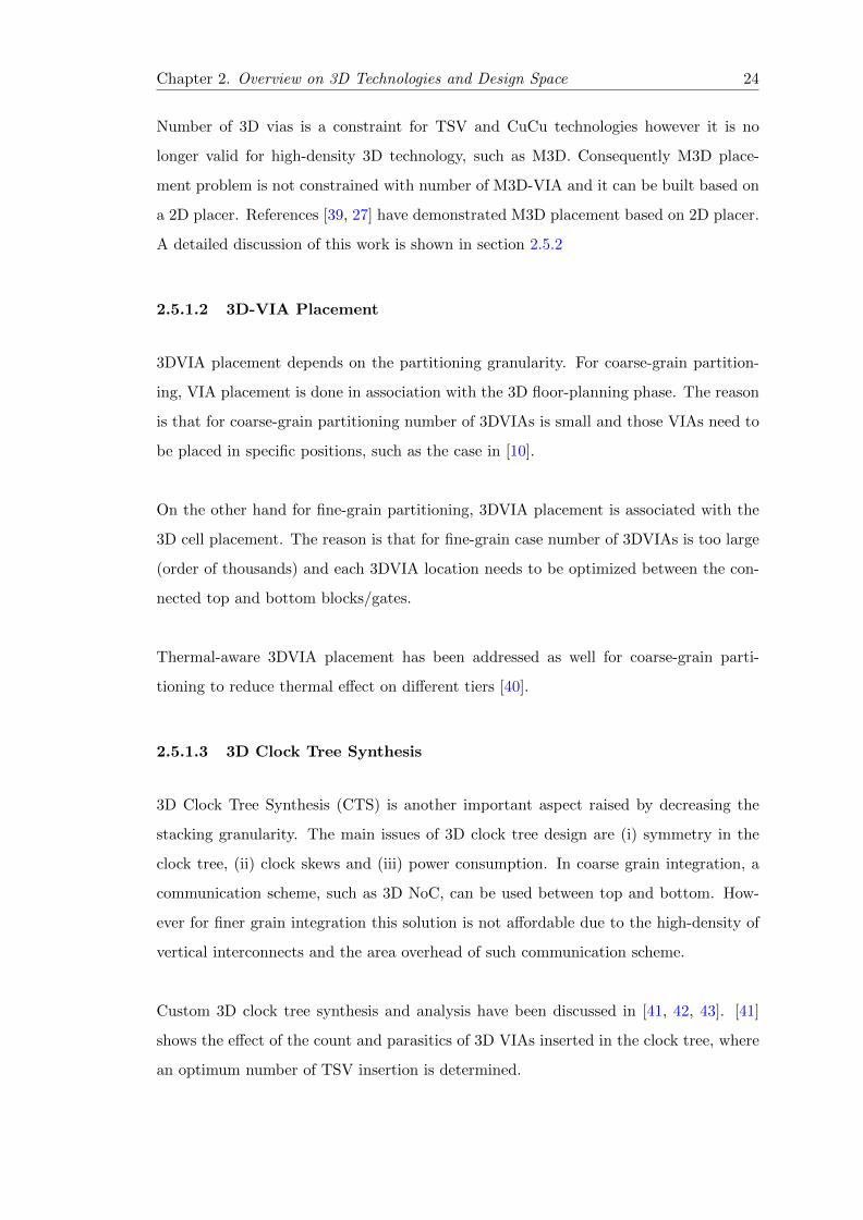
2.4 A qualitative comparison between different 3D clock tree synthesis tech-niques . . . . . . . . . . . . . . . . . . . . . . . . . . . . . . . . . . . . . . 25
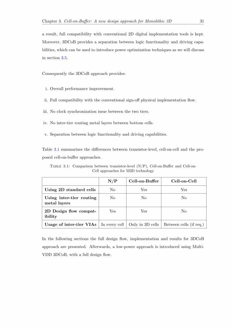
3.1 Comparison between transistor-level (N/P), Cell-on-Buffer and Cell-on-Cell approaches for M3D technology . . . . . . . . . . . . . . . . . . . . . 31
3.2 Validating .LIB generation methodology with a full block implementation.A comparison of implementation results of 128-bit AES block using both.LIB files: the original foundry .LIB file and our generated .LIB file . . . . 40
3.3 Performance optimization results using 3DCoB compared to 2D imple-mentations for openMSP, FFT and AES blocks . . . . . . . . . . . . . . . 41
3.4 Power optimization results using Multi-VDD 3DCoB (β=0.9) implemen-tations for openMSP, FFT and AES blocks . . . . . . . . . . . . . . . . . 47
3.5 Full power-performance comparison between transistor-level (N/P), Cell-on-Buffer and Cell-on-Cell approaches for M3D technology . . . . . . . . . 50
4.1 Comparison between parasitics of M3D-VIA and M2 line of a 28nm CMOStechnology node. . . . . . . . . . . . . . . . . . . . . . . . . . . . . . . . . 52
4.2 Comparing the conventional balanced top/bottom area ratio versus theproposed Unbalanced top/bottom area ratio design techniques for 3D blocks 61
4.3 Results comparison between 2D and 3D cases (hMetis and PAP parti-tioning) for openMSP, Reconf-FFT and LDPC blocks . . . . . . . . . . . 65
5.1 IBEOL flavours power-performance-area results for FFT, FPU and LDPCblocks . . . . . . . . . . . . . . . . . . . . . . . . . . . . . . . . . . . . . . 75
6.1 High-density 3D-Connections parameters . . . . . . . . . . . . . . . . . . 79
6.2 3D connections area penalty for HD-TSV, Cu-Cu and M3D using 28nmFDSOI CMOS technology . . . . . . . . . . . . . . . . . . . . . . . . . . . 84
6.3 Power-Performance results comparison between implementations of 2Dand 3D using M3D and Cu-Cu technologies for openMSP, Reconf-FFTblocks, FPU and LDPC blocks . . . . . . . . . . . . . . . . . . . . . . . . 86
A.1 Total wire length gain in percentage compared to 2D for a given numberof clusters in x and y direction . . . . . . . . . . . . . . . . . . . . . . . . 107
x
List of Tables xi
A.2 Maximal RC delay gain in percentage compared to 2D for a given numberof clusters in x and y direction . . . . . . . . . . . . . . . . . . . . . . . . 107
A.3 The gains obtained for 3D neural cliques used as power managementcontroller. The results are normalized to 2D circuit . . . . . . . . . . . . . 109
B.1 Resultats puissance-performance pour les approches 2D et 3DCoB pourles blocs openMSP, FFT et AES . . . . . . . . . . . . . . . . . . . . . . . 123

Abbreviations
3DCoB 3D Cell on Buffer
3DIC 3D Integrated Circuits
BDP Bi Directional Partitioning
BEOL Back End Of Line
CAD Computer Aided Design
CMOS Complementary Metal Oxide Semiconductor
CuCu Copper-to-Copper
EDA Electronic Design Automation
M3D Monolithic 3D
PAP Physical Aware Partitioning
PPA Power Performance Area
SEM Scanning Electron Microscope
TEM Transmission Electron Microscope
TSV Through Silicon Via
xii
Chapter 1
Introduction
1.1 Context
Scaling limitations and cost of fabrication of advanced CMOS technology nodes are
increasing, resulting in increasingly interest in new technologies to overcome such limi-
tations and continue scaling predicted by Moore’s law [1]. Moore’s law predicts doubling
the number of components, i.e. transistors, per integrated circuit every 1.5-2 years [2].
However continuously scaling and integrating more transistors per chip raise several is-
sues for advanced technology nodes beyond 14nm. New concepts are needed to overcome
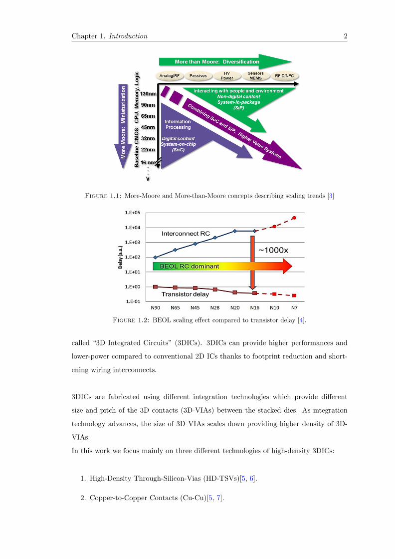
the technology limitations for CMOS scaling. ITRS discussed the technology scaling
roadmap in [3]. Figure 1.1 shows the different scaling directions to enhance system per-
formances. “More-Moore” concept was raised to show the continuous miniaturization
of digital functions while the “More-than-Moore” concept has been raised to show func-
tional diversification by including add-on to the already existing technologies to enhance
the overall chip performances.
The most important impact of technology scaling is the effect of Back-End-Of-Line
(BEOL). By advancing in CMOS node, the gap between delay of the interconnect and
that of transistor is increasing where at 16nm CMOS node delay of interconnect reached
1000x transistor delay [4]. Figure 1.2 illustrates that effect for different CMOS nodes.
One way to overcome technology scaling limitations is to integrate “vertically” by stack-
ing different dies on each other providing a third dimension of scaling. This technique is
1
Chapter 1. Introduction 2
Figure 1.1: More-Moore and More-than-Moore concepts describing scaling trends [3]
Figure 1.2: BEOL scaling effect compared to transistor delay [4].
called “3D Integrated Circuits” (3DICs). 3DICs can provide higher performances and
lower-power compared to conventional 2D ICs thanks to footprint reduction and short-
ening wiring interconnects.
3DICs are fabricated using different integration technologies which provide different
size and pitch of the 3D contacts (3D-VIAs) between the stacked dies. As integration
technology advances, the size of 3D VIAs scales down providing higher density of 3D-
VIAs.
In this work we focus mainly on three different technologies of high-density 3DICs:
1. High-Density Through-Silicon-Vias (HD-TSVs)[5, 6].
2. Copper-to-Copper Contacts (Cu-Cu)[5, 7].
Chapter 1. Introduction 3
3. CoolCubeTM Monolithic 3D Technology (M3D)[8, 9].
The size and pitch of 3D contacts vary for each technology. HD-TSVs technology affords
3D-VIAs of pitch 1.75-10 µm [5, 6], Cu-Cu 3D contact pitch is 2.4-10 µm [5, 7] while
M3D technology scales 3D-VIA pitch down to 0.11µm in 28nm technology node [8].
Detailed discussion on the different 3D technologies is presented in Chapter 2.
1.2 Motivation
As high-density TSV, Cu-Cu and M3D are advanced technologies, there is a need for a
technology assessment framework by implementing 3D designs and evaluating different
technology parameters. CAD tools are well-adapted for 2D place and route, however
there are some issues and limitations using them for 3D implementation. Thus the first
challenge for us is how to create a design methodology to implement blocks using high-
density 3D technologies.
Another important challenge is how to design a 3D block. High-density 3D technologies
affords up to 108 3D vias per mm2 [8]. However each 3D via has resistance and capac-
itance parasitics which lead to power/delay costs. Thus there is an important need to
create a smart partitioning technique to design a 3D block with maximum power and
performance gains.
By having an implementation framework and design methodology, we can create a de-
sign framework to assess different technology parameters from a design perspective. The
technology assessment framework is crucial to be able to provide design-guidelines to
the technology developers, especially for very advanced technologies such as Monolithic
3D.
All the previous points motivate us to introduce a new methodology for 3D technologies
assessment and propose innovative design approaches to highly utilize high-density 3D
technologies.
Chapter 1. Introduction 4
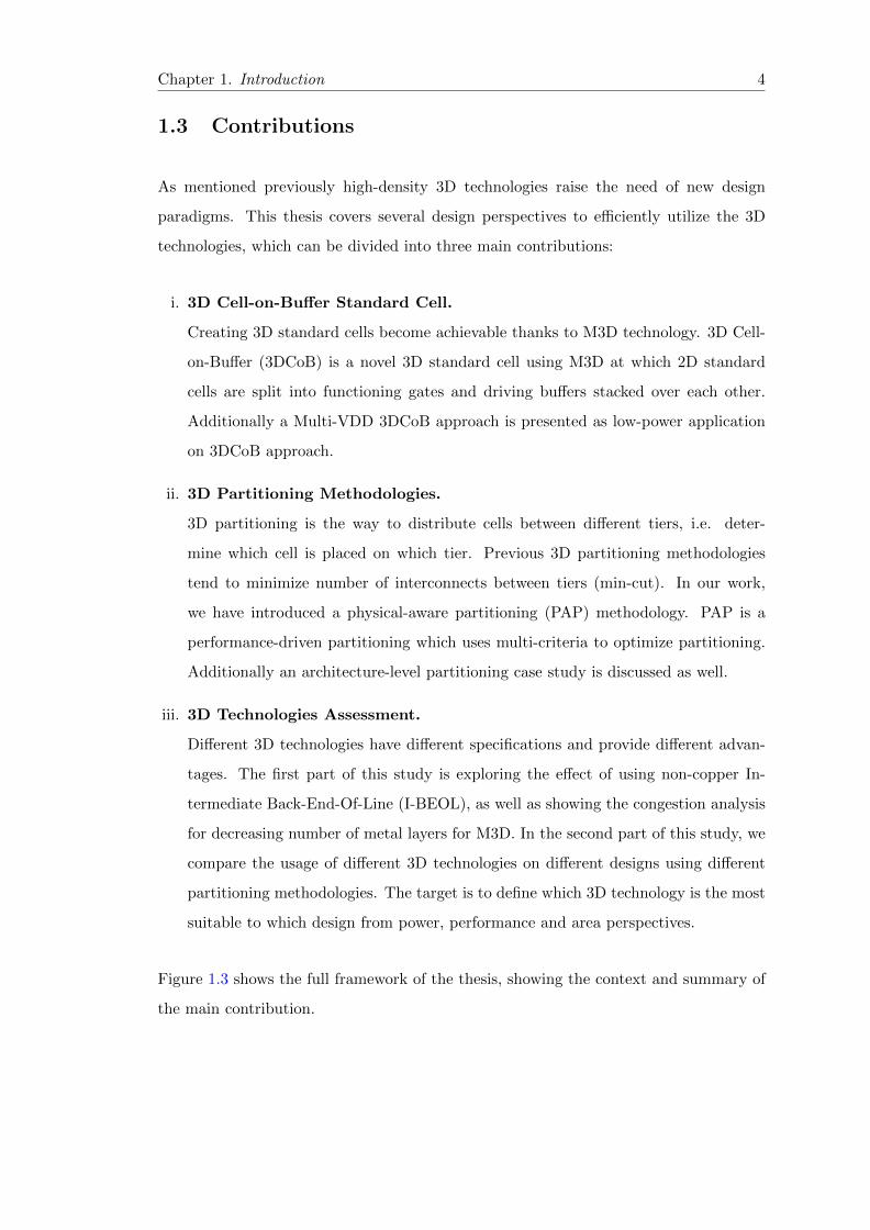
1.3 Contributions
As mentioned previously high-density 3D technologies raise the need of new design
paradigms. This thesis covers several design perspectives to efficiently utilize the 3D
technologies, which can be divided into three main contributions:
i. 3D Cell-on-Buffer Standard Cell.
Creating 3D standard cells become achievable thanks to M3D technology. 3D Cell-
on-Buffer (3DCoB) is a novel 3D standard cell using M3D at which 2D standard
cells are split into functioning gates and driving buffers stacked over each other.
Additionally a Multi-VDD 3DCoB approach is presented as low-power application
on 3DCoB approach.
ii. 3D Partitioning Methodologies.
3D partitioning is the way to distribute cells between different tiers, i.e. deter-
mine which cell is placed on which tier. Previous 3D partitioning methodologies
tend to minimize number of interconnects between tiers (min-cut). In our work,
we have introduced a physical-aware partitioning (PAP) methodology. PAP is a
performance-driven partitioning which uses multi-criteria to optimize partitioning.
Additionally an architecture-level partitioning case study is discussed as well.
iii. 3D Technologies Assessment.
Different 3D technologies have different specifications and provide different advan-
tages. The first part of this study is exploring the effect of using non-copper In-
termediate Back-End-Of-Line (I-BEOL), as well as showing the congestion analysis
for decreasing number of metal layers for M3D. In the second part of this study, we
compare the usage of different 3D technologies on different designs using different
partitioning methodologies. The target is to define which 3D technology is the most
suitable to which design from power, performance and area perspectives.
Figure 1.3 shows the full framework of the thesis, showing the context and summary of
the main contribution.
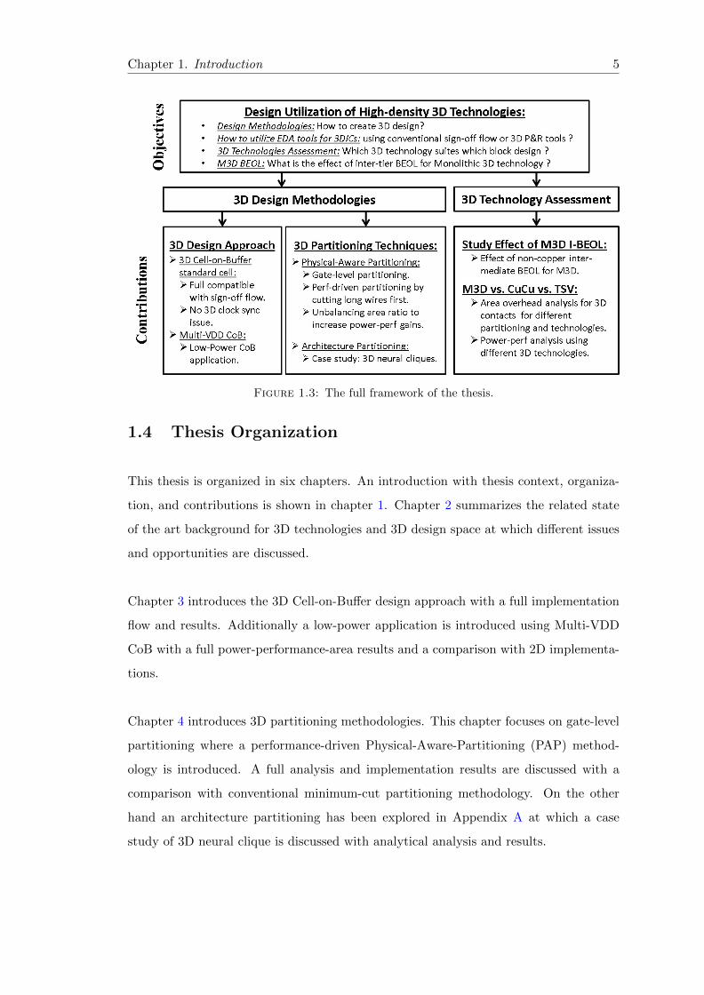
Chapter 1. Introduction 5
Figure 1.3: The full framework of the thesis.
1.4 Thesis Organization
This thesis is organized in six chapters. An introduction with thesis context, organiza-
tion, and contributions is shown in chapter 1. Chapter 2 summarizes the related state
of the art background for 3D technologies and 3D design space at which different issues
and opportunities are discussed.
Chapter 3 introduces the 3D Cell-on-Buffer design approach with a full implementation
flow and results. Additionally a low-power application is introduced using Multi-VDD
CoB with a full power-performance-area results and a comparison with 2D implementa-
tions.
Chapter 4 introduces 3D partitioning methodologies. This chapter focuses on gate-level
partitioning where a performance-driven Physical-Aware-Partitioning (PAP) method-
ology is introduced. A full analysis and implementation results are discussed with a
comparison with conventional minimum-cut partitioning methodology. On the other
hand an architecture partitioning has been explored in Appendix A at which a case
study of 3D neural clique is discussed with analytical analysis and results.
Chapter 1. Introduction 6
Chapter 5 presents a full study of the effect of non-copper metal lines with SiO2 di-
electric used for the Intermediate Back-End-Of-Line (I-BEOL) needed by Monolithic
3D technology using CoolCubeTM process. This study shows effect of increasing resis-
tance and capacitance of the I-BEOL on power-performance metrics with a comparison
with conventional Copper metal lines with low-k dielectric I-BEOL.
Chapter 6 introduces a framework for different 3D technologies assessment. In the chap-
ter a comparison is performed between Monolithic 3D, copper-to-copper and TSV tech-
nologies with (i) area overhead analysis of 3D contacts and (ii) full power-performance-
area results analysis for different implementations. A full discussion of the effect of
different 3D technologies, block designs and partitioning techniques is shown to deter-
mine which 3D technology suites which block design at which partitioning conditions.
A full list of publications is mentioned at the end of this dissertation (Page 133).
Chapter 2
Overview on 3D Technologies and
Design Space
3D design space is large with different parameters from 3D technology, design con-
figuration and CAD tool perspectives. In this chapter we discuss an overview of the
state-of-the-art from these three major aspects; (i) 3D technology spectrum, (ii) stack-
ing granularity, and (iii) issues with 3D CAD tools.
2.1 Why 3D ICs?
Technology scaling faces significant difficulties to keep on following Moore’s law. As
discussed in the introduction, one of the main limitations is the increasing delay of
wiring compared to the delay of transistors [1, 4]. Moreover number of Back End Of
Line (BEOL) design rules is increasing exponentially. One solution to tackle the planar
scaling is to scale vertically by stacking integrated circuits.
3D Integrated Circuits (3D IC) is an emerging technology to stack dies. A direct ad-
vantage of such technology is to decrease the wire length by connecting cells in three
dimensions, as well as: (i) Decreasing area footprint, (ii) Increasing timing performances
by shortening wiring and consequently decreasing the delay of interconnects, (iii) De-
creasing power consumption by decreasing the total wire length, and (iv) Achieving
7
Chapter 2. Overview on 3D Technologies and Design Space 8
heterogeneous integration by stacking different technologies such as memory, digital cir-
cuits, analog circuits, sensors or image display.
3D technology varies with a wide spectrum of capabilities and applications. As we
discussed in the previous chapter, continue technology scaling with Moore’s law, i.e.
More-Moore concept, requires higher density of interconnects. Increasing interconnects
density faces difficulties in the advanced nodes beyond 16nm, such as the need of dou-
ble patterning and Extreme Ultra-Violet (EUV) lithography. One way to scale down
the interconnects and increase their density is by adding a new ‘vertical’ dimension for
routability by using high density 3D technologies. Thanks to high-density 3D technolo-
gies, a very small size of 3D interconnects is achievable which provides the capabilities of
increasing interconnect density. Hence in the following section different 3D technologies
are explored with the focus on the high-density 3D technologies.
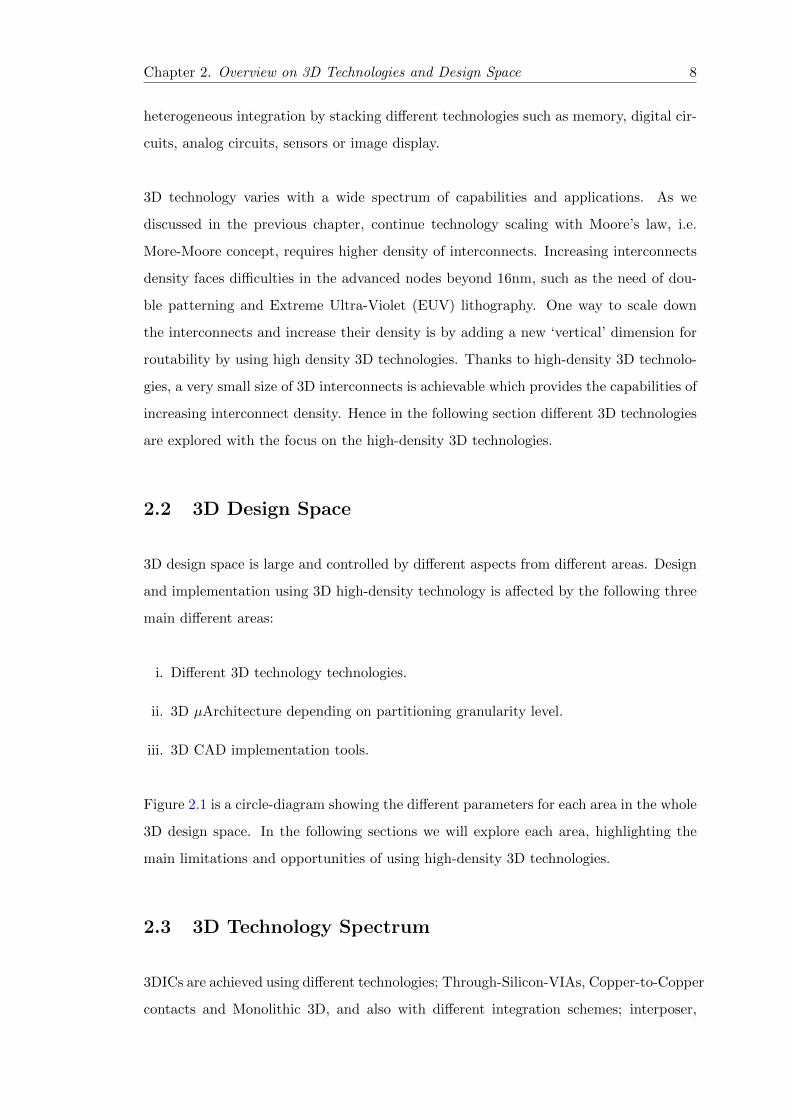
2.2 3D Design Space
3D design space is large and controlled by different aspects from different areas. Design
and implementation using 3D high-density technology is affected by the following three
main different areas:
i. Different 3D technology technologies.
ii. 3D µArchitecture depending on partitioning granularity level.
iii. 3D CAD implementation tools.
Figure 2.1 is a circle-diagram showing the different parameters for each area in the whole
3D design space. In the following sections we will explore each area, highlighting the
main limitations and opportunities of using high-density 3D technologies.
2.3 3D Technology Spectrum
3DICs are achieved using different technologies; Through-Silicon-VIAs, Copper-to-Copper
contacts and Monolithic 3D, and also with different integration schemes; interposer,
Chapter 2. Overview on 3D Technologies and Design Space 9
Figure 2.1: High-Density 3D Design Space.
face-to-back and face-to-face configurations. This section summarizes the 3D technol-
ogy spectrum where the first subsection introduces different 3D integration schemes and
the subsections after explore the different 3D technologies.
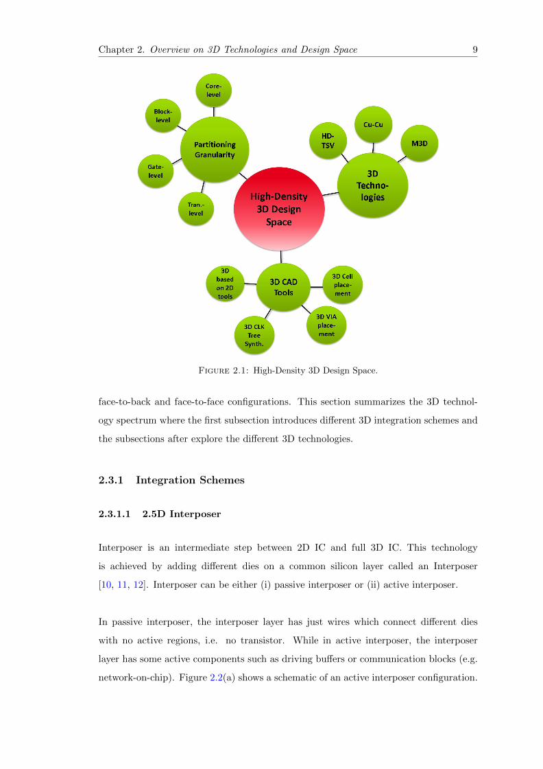
2.3.1 Integration Schemes
2.3.1.1 2.5D Interposer
Interposer is an intermediate step between 2D IC and full 3D IC. This technology
is achieved by adding different dies on a common silicon layer called an Interposer
[10, 11, 12]. Interposer can be either (i) passive interposer or (ii) active interposer.
In passive interposer, the interposer layer has just wires which connect different dies
with no active regions, i.e. no transistor. While in active interposer, the interposer
layer has some active components such as driving buffers or communication blocks (e.g.
network-on-chip). Figure 2.2(a) shows a schematic of an active interposer configuration.
Chapter 2. Overview on 3D Technologies and Design Space 10
Interposer technology is mainly targeting by big circuits such as micro-servers and com-
munication chips. The motivation is to reduce the silicon area by splitting the chip into
chiplets integrated on an interposer which can increase yield, reduce costs, and enable
heterogeneous integration by having different CMOS technology node for each chiplet.
2.3.1.2 3D Configurations: Face-to-Back and Face-to-Face
3D integration can be either face-to-face (F2F) or face-to-back (F2B). In this context
we are considering each die has a face and a back, where the face of a die is the top
metal layer and the back of a die is the silicon substrate. Consequently the dies can
be stacked in a F2F configuration so that the top metal layers are facing each other.
Each integration scheme requires different 3D technology to connect the top and bottom
dies as we will explain in the next sections. Figure 2.2(b) and (c) show F2B and F2F
configuration respectively.
(a)
(b) (c)
Figure 2.2: Different integration schemes, (a) 2.5D active interposer schematic [10],(b) 3D Face-to-Back configuration, (c) 3D Face-to-Face configuration.
Chapter 2. Overview on 3D Technologies and Design Space 11
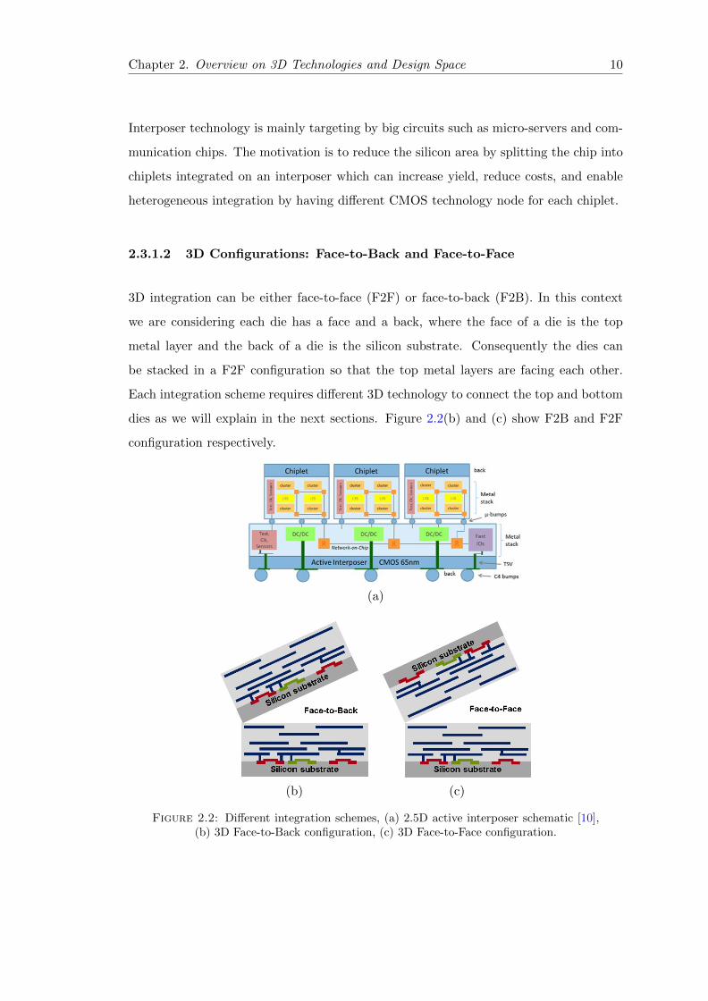
2.3.2 3D Through-Silicon-VIA Technology
Through silicon vias (TSV) is a 3D technology at which the 3D via is used for connec-
tions through the silicon substrate. One application for TSVs is to connect metal layers
of the bottom die to the top die for a face-to-back configuration. Another usage can be
connecting metal layers with substrate µbumps for IO and Power connections.
The diameter and pitch of TSVs determine the density limit of 3D connections that
can be achieved. However, the dimensions of TSV are controlled by the assembly pro-
cess used to stack the dies over each others. Conventional 3D TSV technologies have
TSVs with a diameter of 10-20 µm. With the advances of assembly process, 3D TSVs
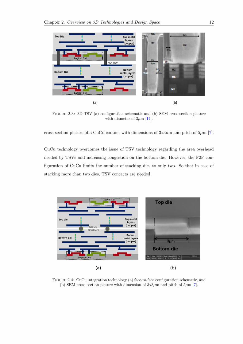
diameter can scale down to 3µm [13, 6]. Figure 2.3 shows a schematic of face-to-back
stacking configuration using TSV connection with a SEM cross-section picture of a 3µm
diameter TSV [14].
The constraints of TSV technology at Design level are the spacing needed for the TSV
on the top die which will increase the area overhead and can affect the resultant wire
length. To illustrate this area overhead effect, we can mention that High-density TSVs
with 5µm and 10µm pitches have an equivalent area of 5 and 20 Flip Flops, respectively,
in 28nm Technology. Another constraint is the routing on the bottom die where the
routing congestion will increase due to the presence of TSVs which cut vertically the
bottom metal layers.
2.3.3 3D Copper-to-Copper Technology
Copper-to-copper (CuCu) contact is another 3D integration technology where the two
dies are fabricated separately (in parallel) and then assembled together, which is similar
to the TSV technology. However CuCu technology is used in F2F stacking configura-
tion. The 3D connections are achieved by direct bonding of top and bottom dies using
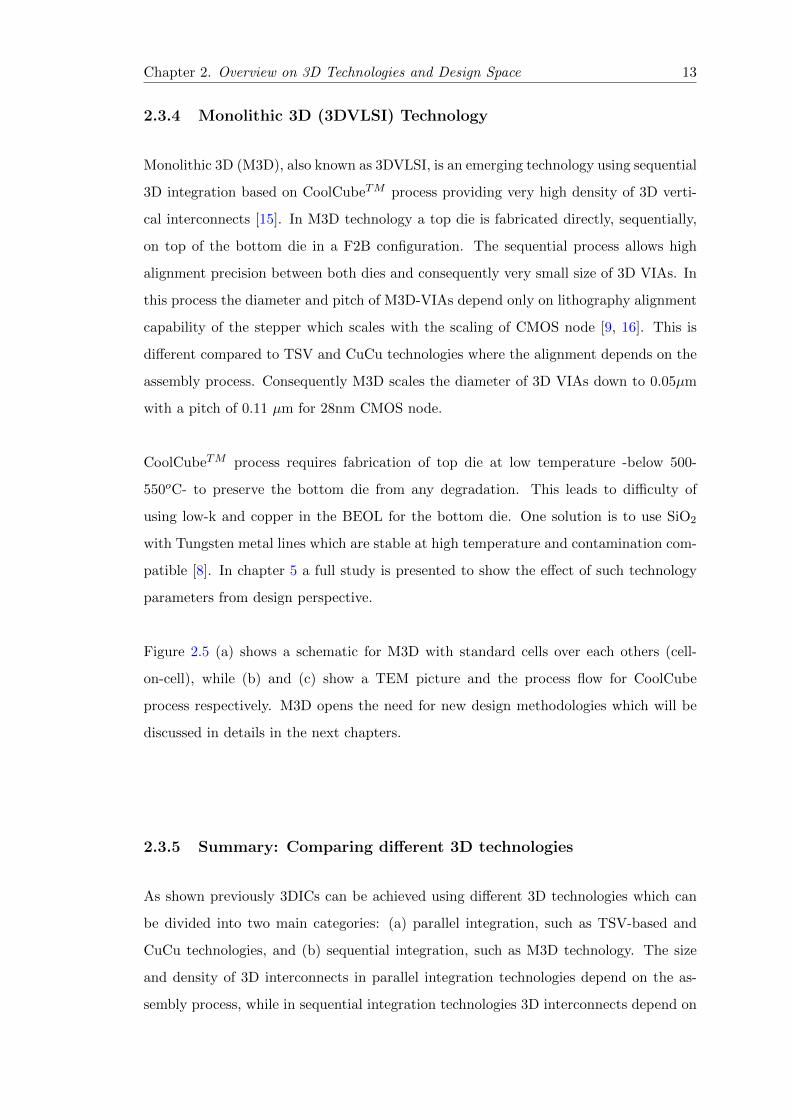
copper contacts on top of each metal layer stack. The pitch between CuCu 3D contacts
can be scaled down to 3.4-5µm[5, 7]. Figure 2.4 (a) shows a schematic for face-to-face
configuration using CuCu integration technology, where (b) shows a fabricated SEM
Chapter 2. Overview on 3D Technologies and Design Space 12
Figure 2.3: 3D-TSV (a) configuration schematic and (b) SEM cross-section picturewith diameter of 3µm [14].
cross-section picture of a CuCu contact with dimensions of 3x3µm and pitch of 5µm [7].
CuCu technology overcomes the issue of TSV technology regarding the area overhead
needed by TSVs and increasing congestion on the bottom die. However, the F2F con-
figuration of CuCu limits the number of stacking dies to only two. So that in case of
stacking more than two dies, TSV contacts are needed.
Figure 2.4: CuCu integration technology (a) face-to-face configuration schematic, and(b) SEM cross-section picture with dimension of 3x3µm and pitch of 5µm [7].
Chapter 2. Overview on 3D Technologies and Design Space 13
2.3.4 Monolithic 3D (3DVLSI) Technology
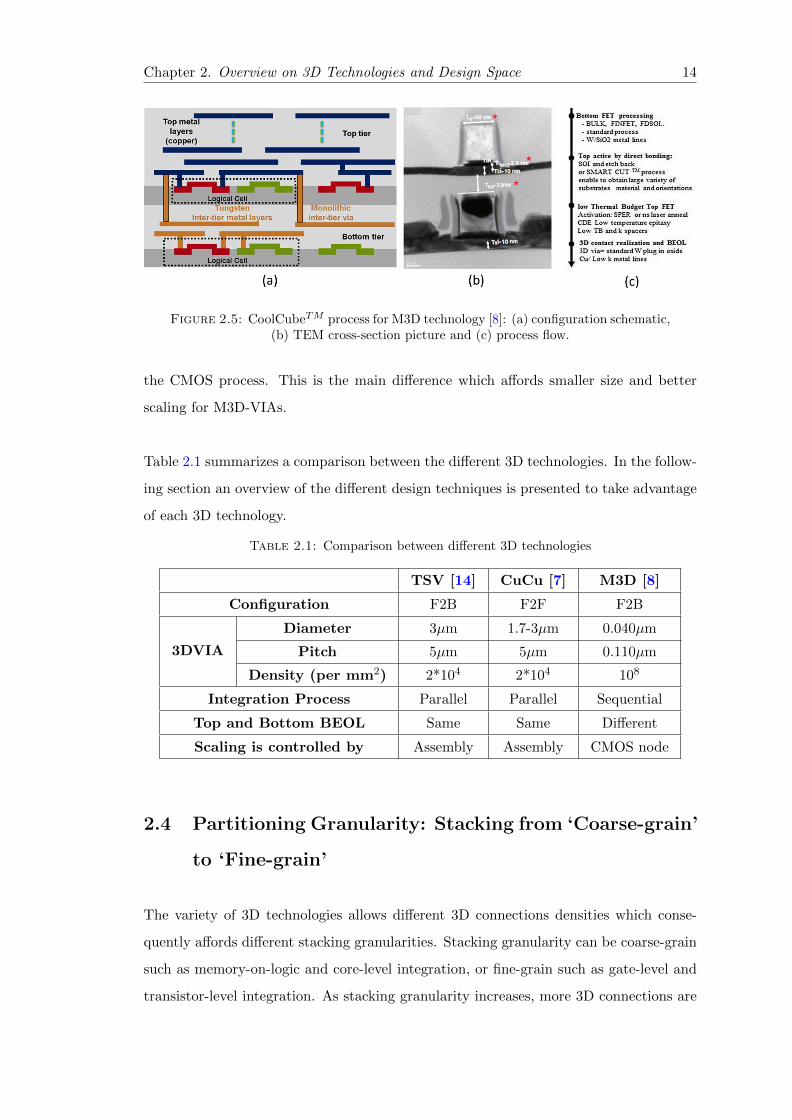
Monolithic 3D (M3D), also known as 3DVLSI, is an emerging technology using sequential
3D integration based on CoolCubeTM process providing very high density of 3D verti-
cal interconnects [15]. In M3D technology a top die is fabricated directly, sequentially,
on top of the bottom die in a F2B configuration. The sequential process allows high
alignment precision between both dies and consequently very small size of 3D VIAs. In
this process the diameter and pitch of M3D-VIAs depend only on lithography alignment
capability of the stepper which scales with the scaling of CMOS node [9, 16]. This is
different compared to TSV and CuCu technologies where the alignment depends on the
assembly process. Consequently M3D scales the diameter of 3D VIAs down to 0.05µm
with a pitch of 0.11 µm for 28nm CMOS node.
CoolCubeTM process requires fabrication of top die at low temperature -below 500-
550oC- to preserve the bottom die from any degradation. This leads to difficulty of
using low-k and copper in the BEOL for the bottom die. One solution is to use SiO2
with Tungsten metal lines which are stable at high temperature and contamination com-
patible [8]. In chapter 5 a full study is presented to show the effect of such technology
parameters from design perspective.
Figure 2.5 (a) shows a schematic for M3D with standard cells over each others (cell-
on-cell), while (b) and (c) show a TEM picture and the process flow for CoolCube
process respectively. M3D opens the need for new design methodologies which will be
discussed in details in the next chapters.
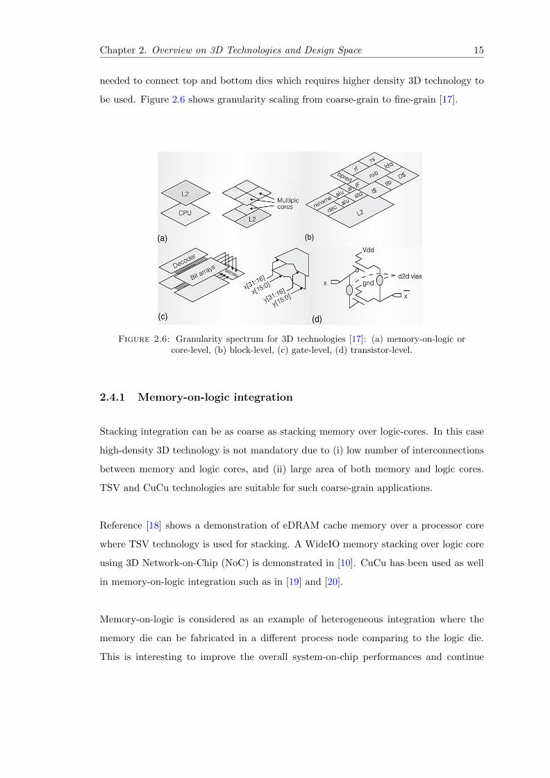
2.3.5 Summary: Comparing different 3D technologies
As shown previously 3DICs can be achieved using different 3D technologies which can
be divided into two main categories: (a) parallel integration, such as TSV-based and
CuCu technologies, and (b) sequential integration, such as M3D technology. The size
and density of 3D interconnects in parallel integration technologies depend on the as-
sembly process, while in sequential integration technologies 3D interconnects depend on
Chapter 2. Overview on 3D Technologies and Design Space 14
Figure 2.5: CoolCubeTM process for M3D technology [8]: (a) configuration schematic,(b) TEM cross-section picture and (c) process flow.
the CMOS process. This is the main difference which affords smaller size and better
scaling for M3D-VIAs.
Table 2.1 summarizes a comparison between the different 3D technologies. In the follow-
ing section an overview of the different design techniques is presented to take advantage
of each 3D technology.
Table 2.1: Comparison between different 3D technologies
TSV [14] CuCu [7] M3D [8]
Configuration F2B F2F F2B
3DVIA
Diameter 3µm 1.7-3µm 0.040µm
Pitch 5µm 5µm 0.110µm
Density (per mm2) 2*104 2*104 108
Integration Process Parallel Parallel Sequential
Top and Bottom BEOL Same Same Different
Scaling is controlled by Assembly Assembly CMOS node
2.4 Partitioning Granularity: Stacking from ‘Coarse-grain’
to ‘Fine-grain’
The variety of 3D technologies allows different 3D connections densities which conse-
quently affords different stacking granularities. Stacking granularity can be coarse-grain
such as memory-on-logic and core-level integration, or fine-grain such as gate-level and
transistor-level integration. As stacking granularity increases, more 3D connections are
Chapter 2. Overview on 3D Technologies and Design Space 15
needed to connect top and bottom dies which requires higher density 3D technology to
be used. Figure 2.6 shows granularity scaling from coarse-grain to fine-grain [17].
Figure 2.6: Granularity spectrum for 3D technologies [17]: (a) memory-on-logic orcore-level, (b) block-level, (c) gate-level, (d) transistor-level.
2.4.1 Memory-on-logic integration
Stacking integration can be as coarse as stacking memory over logic-cores. In this case
high-density 3D technology is not mandatory due to (i) low number of interconnections
between memory and logic cores, and (ii) large area of both memory and logic cores.
TSV and CuCu technologies are suitable for such coarse-grain applications.
Reference [18] shows a demonstration of eDRAM cache memory over a processor core
where TSV technology is used for stacking. A WideIO memory stacking over logic core
using 3D Network-on-Chip (NoC) is demonstrated in [10]. CuCu has been used as well
in memory-on-logic integration such as in [19] and [20].
Memory-on-logic is considered as an example of heterogeneous integration where the
memory die can be fabricated in a different process node comparing to the logic die.
This is interesting to improve the overall system-on-chip performances and continue
Chapter 2. Overview on 3D Technologies and Design Space 16
with More-than-Moore trend, however, our interest is to use high-density 3D technolo-
gies for logic-on-logic stacking to be able to integrate more transistors and continue
miniaturization with More-Moore trend.
2.4.2 Core-level and block-level integration
Logic-on-logic integration can be achieved as well at different granularities. A coarse-
grain can be achieved by stacking logic cores over each other. Reference [21] discussed
the extension of memory-on-logic 3DICs to several layers 3DICs including core-level in-
tegration. References [22, 23] discussed different design aspects for core-level integration.
A finer grain stacking can be achieved by splitting a specific core and integrate its internal
blocks over each other, which is called ‘block-level integration’. References [17] and [24]
discuss two case studies for block-level integration of Intel Pentium 4 and openSPARC
T2 processors respectively. Figure 2.7 shows the detailed block-level integration of an
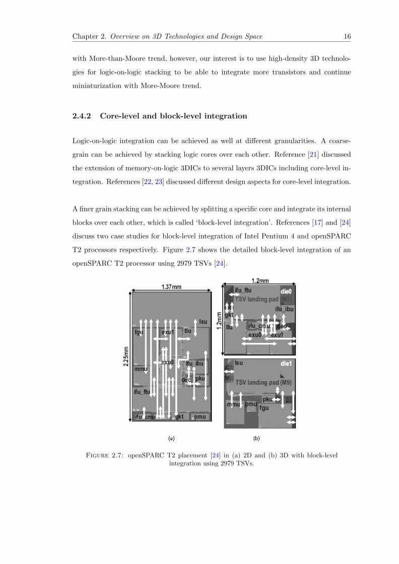
openSPARC T2 processor using 2979 TSVs [24].
Figure 2.7: openSPARC T2 placement [24] in (a) 2D and (b) 3D with block-levelintegration using 2979 TSVs.
Chapter 2. Overview on 3D Technologies and Design Space 17
2.4.3 Gate-level integration (Cell-on-Cell)
Gate-level integration, or Cell-on-Cell, is achieved by stacking standard cells over each
others. As the density of connections between standard cells is much higher than that be-
tween blocks or cores, a high-density 3D technology is needed for cell-on-cell integration.
Cell-on-Cell raises the need for a proper partitioning methodology to determine which
standard cell is assigned to which die. A min-cut partitioning algorithm is proposed
in [25] to minimize number of connections between dies, and has been used in [26] to
demonstrate the stacking of a DSP block using CuCu technology. A placement-driven
partitioning algorithm has been proposed in [27] to increase the benefits of M3D technol-
ogy. A detailed discussion on the gate-level partitioning algorithm is shown in Chapter 4.
Additionally the gate-level integration granularity increases the need for a 3D clock
tree synthesis and an optimized 3D cell placement. These two aspects are needed for
block-level as well however they become more critical for finer granularities. Both issues
will be discussed in details in the next section (sec.2.5).
2.4.4 Transistor-level integration (N/P)
Transistor-level integration is the finest stacking approach in the granularity spectrum.
It is achieved by splitting each CMOS gate in two parts, so that NMOS and PMOS
transistors are placed in different layers (N/P). A very high density 3D technology, such
as M3D, is needed to achieve N/P approach. The main advantages of N/P approach
are:
1. (+) Perform process optimization for each transistor layer separately.
2. (+) Minimize number of metal layers of the bottom die as all cell routing is done
in the top die.
3. (+) By designing libraries of new 3D standard cells, conventional 2D EDA tool
flow can be used.
On the other hand, N/P approach has some drawback such as:
Chapter 2. Overview on 3D Technologies and Design Space 18
1. (-) N/P approach requires insertion of 3DVIA in each cell which increase the
internal resistance and capacitance parasitics of standard cells.
2. (-) The need to re-design and characterize all the 2D design kit libraries to create
new 3D standard cells.
3. (-) Limited to two-tiers only. If more than two tiers are used, a cell-on-cell ap-
proach is needed.
Reference [28, 29] discuss the benefits and challenges of N/P approach using Monolithic
3D technology for logic blocks (e.g. AES, FFT, JPEG).
Creating a 3D SRAM cell using transistor-level stacking is another design paradigm
which has been explored in [30, 31].
2.4.5 Logic-on-Logic stacking: Fine vs. Coarse grain Partitioning
As we illustrated, partitioning techniques differ according to the stacking granularity
used. Logic-on-Logic stacking can be divided into two main categories: (i) Architecture-
level Partitioning for a coarse-grain stacking, and (ii) Gate-level partitioning for fine-
grain stacking.
2.4.5.1 Coarse-Grain: Architecture-level Partitioning
Coarse grain stacking is used for technologies with large 3D-VIA diameter and pitch.
In this case an ‘Architecture-level partitioning’ is needed where the global interconnects
are cut and converted into 3D connections. These global interconnects can be between
memories and logic blocks, or between cores in a many-core architectures, or even be-
tween main functional parts of a logic block.
Architecture-level partitioning approach requires the designer to have a preliminary
good knowledge and understanding of the 2D architecture, and consequently it takes
long time that is not compatible with complex and large-scale designs. Memory-on-logic
partitioning has been demonstrated in [18, 19, 20, 21], while logic-on-logic stacking using
architecture-level partitioning has been demonstrated in [17, 32, 24, 33, 34].
Chapter 2. Overview on 3D Technologies and Design Space 19
2.4.5.2 Fine-Grain: Gate-level Partitioning
As 3D technology advances, diameter and pitch of 3D-VIA decrease which allow higher
density 3D contacts. Fine grain partitioning is achievable thanks to such high-density
3D technology. The partitioning granularity can be as fine as cell-on-cell stacking, i.e.
gate-level.
(a)
(b) (c)
Figure 2.8: An example of 5 standard cell netlist where a gate-level partitioning isneeded to decide which gate (standard cell) is assigned to the top tier and which to thebottom. The objective is to determine which partition gives better power-performance-
area results (b) or (c) ?
Using such high-density technology, a ‘Gate-level partitioning’ technique is needed to
distribute the standard cells across top and bottom tiers which creates a cell-on-cell 3D
stacking. Gate-level partitioning produces large number of 3D contacts (order of ten-
s/hundreds of thousands) per mm2. Conventional architecture-level partitioning has two
issues with high-density technology: (i) long design time due to the fine-grain stacking
which increases the time-to-market cycle (ii) limiting the gains of such high-density 3D
technologies due to limiting number of 3D contacts by cutting only global 2D intercon-
nects.
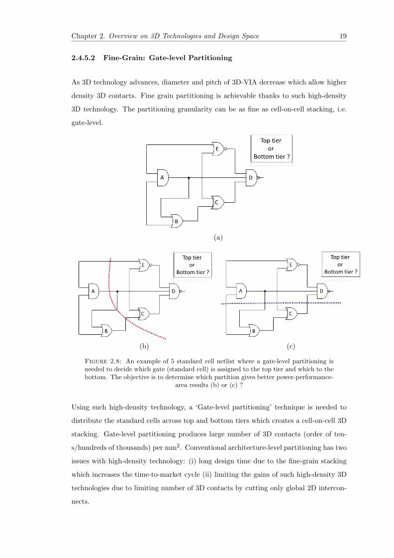
Chapter 2. Overview on 3D Technologies and Design Space 20
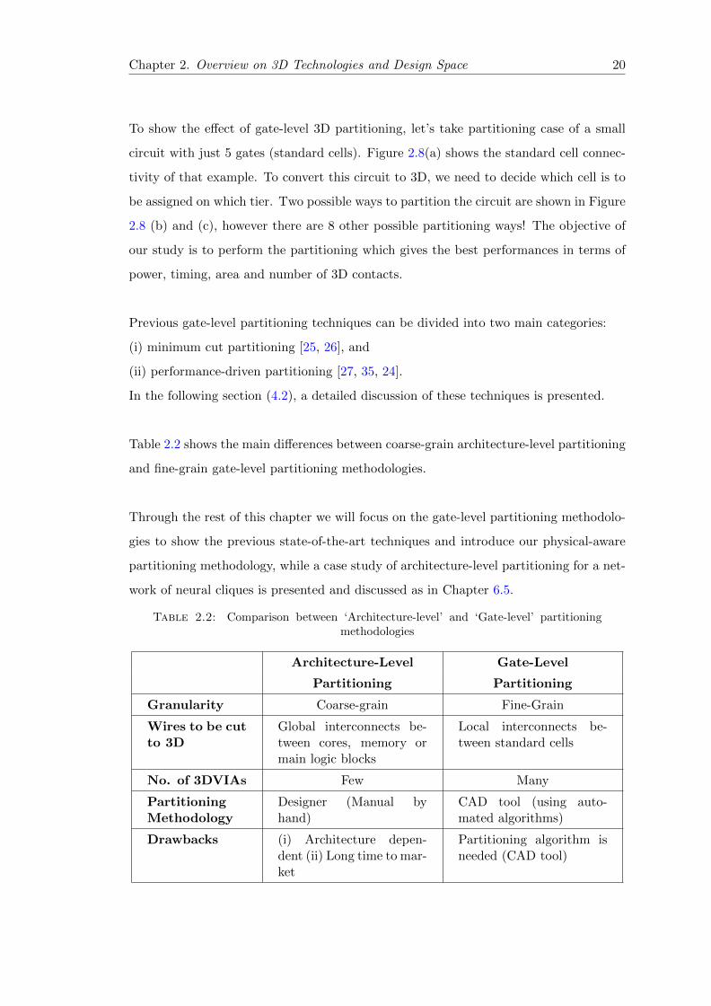
To show the effect of gate-level 3D partitioning, let’s take partitioning case of a small
circuit with just 5 gates (standard cells). Figure 2.8(a) shows the standard cell connec-
tivity of that example. To convert this circuit to 3D, we need to decide which cell is to
be assigned on which tier. Two possible ways to partition the circuit are shown in Figure
2.8 (b) and (c), however there are 8 other possible partitioning ways! The objective of
our study is to perform the partitioning which gives the best performances in terms of
power, timing, area and number of 3D contacts.
Previous gate-level partitioning techniques can be divided into two main categories:
(i) minimum cut partitioning [25, 26], and
(ii) performance-driven partitioning [27, 35, 24].
In the following section (4.2), a detailed discussion of these techniques is presented.
Table 2.2 shows the main differences between coarse-grain architecture-level partitioning
and fine-grain gate-level partitioning methodologies.
Through the rest of this chapter we will focus on the gate-level partitioning methodolo-
gies to show the previous state-of-the-art techniques and introduce our physical-aware
partitioning methodology, while a case study of architecture-level partitioning for a net-
work of neural cliques is presented and discussed as in Chapter 6.5.
Table 2.2: Comparison between ‘Architecture-level’ and ‘Gate-level’ partitioningmethodologies
Architecture-Level Gate-Level
Partitioning Partitioning
Granularity Coarse-grain Fine-Grain
Wires to be cutto 3D
Global interconnects be-tween cores, memory ormain logic blocks
Local interconnects be-tween standard cells
No. of 3DVIAs Few Many
PartitioningMethodology
Designer (Manual byhand)
CAD tool (using auto-mated algorithms)
Drawbacks (i) Architecture depen-dent (ii) Long time to mar-ket
Partitioning algorithm isneeded (CAD tool)
Chapter 2. Overview on 3D Technologies and Design Space 21
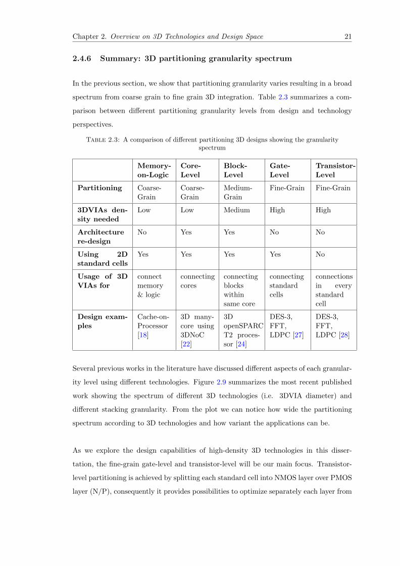
2.4.6 Summary: 3D partitioning granularity spectrum
In the previous section, we show that partitioning granularity varies resulting in a broad
spectrum from coarse grain to fine grain 3D integration. Table 2.3 summarizes a com-
parison between different partitioning granularity levels from design and technology
perspectives.
Table 2.3: A comparison of different partitioning 3D designs showing the granularityspectrum
Memory-on-Logic
Core-Level
Block-Level
Gate-Level
Transistor-Level
Partitioning Coarse-Grain
Coarse-Grain
Medium-Grain
Fine-Grain Fine-Grain
3DVIAs den-sity needed
Low Low Medium High High
Architecturere-design
No Yes Yes No No
Using 2Dstandard cells
Yes Yes Yes Yes No
Usage of 3DVIAs for
connectmemory& logic
connectingcores
connectingblockswithinsame core
connectingstandardcells
connectionsin everystandardcell
Design exam-ples
Cache-on-Processor[18]
3D many-core using3DNoC[22]
3DopenSPARCT2 proces-sor [24]
DES-3,FFT,LDPC [27]
DES-3,FFT,LDPC [28]
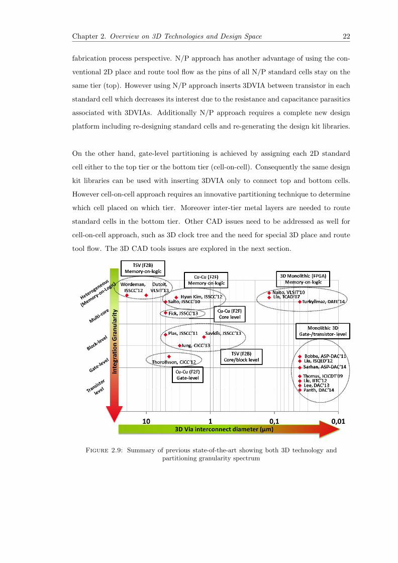
Several previous works in the literature have discussed different aspects of each granular-
ity level using different technologies. Figure 2.9 summarizes the most recent published
work showing the spectrum of different 3D technologies (i.e. 3DVIA diameter) and
different stacking granularity. From the plot we can notice how wide the partitioning
spectrum according to 3D technologies and how variant the applications can be.
As we explore the design capabilities of high-density 3D technologies in this disser-
tation, the fine-grain gate-level and transistor-level will be our main focus. Transistor-
level partitioning is achieved by splitting each standard cell into NMOS layer over PMOS
layer (N/P), consequently it provides possibilities to optimize separately each layer from
Chapter 2. Overview on 3D Technologies and Design Space 22
fabrication process perspective. N/P approach has another advantage of using the con-
ventional 2D place and route tool flow as the pins of all N/P standard cells stay on the
same tier (top). However using N/P approach inserts 3DVIA between transistor in each
standard cell which decreases its interest due to the resistance and capacitance parasitics
associated with 3DVIAs. Additionally N/P approach requires a complete new design
platform including re-designing standard cells and re-generating the design kit libraries.
On the other hand, gate-level partitioning is achieved by assigning each 2D standard
cell either to the top tier or the bottom tier (cell-on-cell). Consequently the same design
kit libraries can be used with inserting 3DVIA only to connect top and bottom cells.
However cell-on-cell approach requires an innovative partitioning technique to determine
which cell placed on which tier. Moreover inter-tier metal layers are needed to route
standard cells in the bottom tier. Other CAD issues need to be addressed as well for
cell-on-cell approach, such as 3D clock tree and the need for special 3D place and route
tool flow. The 3D CAD tools issues are explored in the next section.
Figure 2.9: Summary of previous state-of-the-art showing both 3D technology andpartitioning granularity spectrum
Chapter 2. Overview on 3D Technologies and Design Space 23
2.5 3D CAD Tools: Issues and Perspectives
In the previous two sections 3D technologies and stacking granularity spectrum have
been explored. To complete the design cycle CAD tools suited for 3D are needed to
implement 3D designs using the proper technology. CAD tools have different require-
ments for 3DICs than for 2DICs, and these requirements vary according to the design
granularity. Several previous works have addressed different issues of CAD tools for 3D.
In this section we will first discuss the issues for 3D CAD tools with previous solutions
and then we will show some techniques to use 2D commercial tool flow to implement a
3D design.
2.5.1 Issues of CAD tools for 3DICs
EDA design and implementation flow is mature for 2D ICs using several commercial
CAD tools however for 3D there are different issues compared to 2D. In the follow-
ing subsections 3D cell placement, 3DVIA placement and 3D clock tree synthesis are
discussed.
2.5.1.1 3D Standard Cell Placement
Generally standard cell placement is a critical phase in a design implementation. Due to
the increasing complexity of integrated circuits, placement is divided into three phases:
(i) global placement; where the standard cells are placed within a relaxed overlap con-
strain, (ii) placement legalization; where any cell overlapping is removed and cell place-
ment is legalized, (iii) detailed placement; where placement is further improved with a
non-overlapping constraint using cell swapping and re-arrangement techniques.
For 3D standard cell placement, references [36, 37, 38] proposed analytical full 3D global
placement algorithms. These algorithms are based on generating an optimization func-
tion in three-dimensions (x, y, z) which targets minimizing wire length and number of 3D
vias (TSVs). These techniques are effective to compromise between decreasing number
of 3D vias and achieving minimum wire length.
Chapter 2. Overview on 3D Technologies and Design Space 24
Number of 3D vias is a constraint for TSV and CuCu technologies however it is no
longer valid for high-density 3D technology, such as M3D. Consequently M3D place-
ment problem is not constrained with number of M3D-VIA and it can be built based on
a 2D placer. References [39, 27] have demonstrated M3D placement based on 2D placer.
A detailed discussion of this work is shown in section 2.5.2
2.5.1.2 3D-VIA Placement
3DVIA placement depends on the partitioning granularity. For coarse-grain partition-
ing, VIA placement is done in association with the 3D floor-planning phase. The reason
is that for coarse-grain partitioning number of 3DVIAs is small and those VIAs need to
be placed in specific positions, such as the case in [10].
On the other hand for fine-grain partitioning, 3DVIA placement is associated with the
3D cell placement. The reason is that for fine-grain case number of 3DVIAs is too large
(order of thousands) and each 3DVIA location needs to be optimized between the con-
nected top and bottom blocks/gates.
Thermal-aware 3DVIA placement has been addressed as well for coarse-grain parti-
tioning to reduce thermal effect on different tiers [40].
2.5.1.3 3D Clock Tree Synthesis
3D Clock Tree Synthesis (CTS) is another important aspect raised by decreasing the
stacking granularity. The main issues of 3D clock tree design are (i) symmetry in the
clock tree, (ii) clock skews and (iii) power consumption. In coarse grain integration, a
communication scheme, such as 3D NoC, can be used between top and bottom. How-
ever for finer grain integration this solution is not affordable due to the high-density of
vertical interconnects and the area overhead of such communication scheme.
Custom 3D clock tree synthesis and analysis have been discussed in [41, 42, 43]. [41]
shows the effect of the count and parasitics of 3D VIAs inserted in the clock tree, where
an optimum number of TSV insertion is determined.
Chapter 2. Overview on 3D Technologies and Design Space 25
However a full 3D clock synthesis lacks the support of CAD tools. Some techniques
have been proposed to avoid synthesizing a 3D clock tree. One technique is to create
two clock trees on each die, separately, with a Digital Locked Loop (DLL) for synchro-
nization and skew removal. The cost of this technique is the extra area overhead for
implementing DLLs on each die [44]. Another technique is to create shorted-clock-tree
to remove the skew between top and bottom at the cost of extra power [44]. Reference
[45] shows a demonstration of different conventional clock topologies implemented in
3-layers 3D chip including; H-tree over H-tree, H-tree over global-rings and H-tree over
local-rings.
Targeting fine-grain gate-level partitioning using high-density 3D technology opens a
new technique to avoid 3D CTS issue. The method is to place all flip-flops only on
one die. However a dedicated gate-level partitioning algorithm is needed for that. This
technique has been used in [26].
Table 2.4 shows a qualitative comparison between the different 3D clock tree techniques.
Table 2.4: A qualitative comparison between different 3D clock tree synthesis tech-niques
H-Tree/H-Tree[45]
DLL-Based[44]
Short-Circuit[44]
Custom3D CTS[41, 42, 43]
CLK treeonly on onetier [26]
3DVIA count High Low High Depends onCTS alg.
0
3D CLK Skew Low Med(DLL)
Low Low -NA-
3D CLK Power High Med(DLL)
High Low -NA-
Design Overhead No DLL No 3D CTS alg. 3D Parti-tioning
Suitable StackingGranularity
All All* All All Gate-level
* Shared DLL is needed for block-/gate- level granularity to minimize DLL overhead
Chapter 2. Overview on 3D Technologies and Design Space 26
2.5.2 3D Implementation based on 2D Commercial Tools
With the lack of mature 3D implementation tools and the need for implementation re-
sults using sign-off flow, several work used conventional 2D tool flow to implement 3D
designs, which takes advantage of using mature tools and makes integrating 3D place-
ment into conventional flow much easier.
For 3D placement, some simple techniques can be used to convert a 2D placement to a
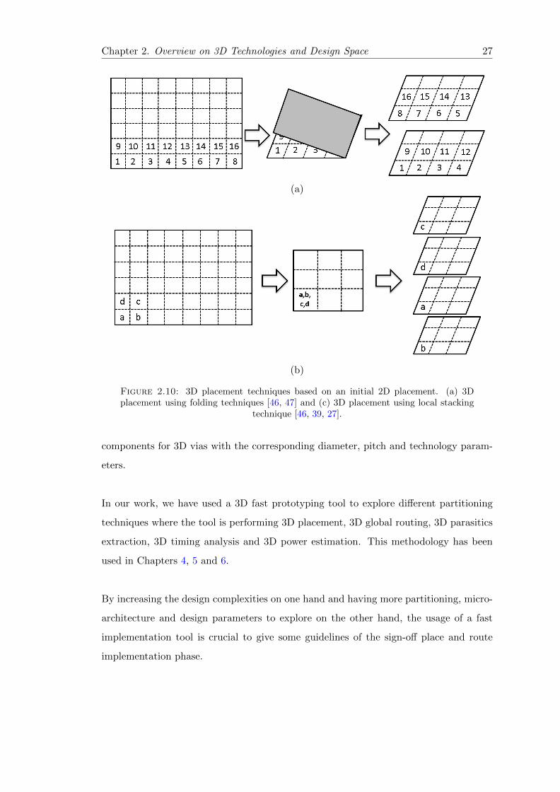
3D one as shown in Figure 2.10. One straight-forward technique is 2D folding as used
in [46, 47]. Another way is by local stacking transformation and window-based stacking
transformation [46, 39, 27]. In 2D folding technique, the long wires are shortened by
stacking the far cells over each others, while in local stacking technique; close cells are
stacked over each other.
To achieve local stacking technique, ‘CELONCEL’ approach [39] is introduced where
a 3D placement technique is performed by three steps: (i) transforming each standard
cell to half its size, (ii) these cells are placed using regular 2D placer, and then (iii)
restore the standard cells to their original size. ‘Shrunk2D’ is a similar technique to
provide a placement-driven partitioning for M3D which has been proposed in [27].
2.5.3 Using Fast Prototyping Implementation Tool
As we have illustrated partitioning techniques are needed to distribute the standard
cells across top and bottom tiers. However for complex designs, several 3D partitioned
and micro-architecture options require evaluation which takes long run time by using
conventional place and route as a full sign-off physical implementation tools. Hence the
need for a fast prototyping tool is increasing to explore the different design variabilities
within acceptable short run time. For example, an FFT block takes 4.5x run time by
using a full place and route tool comparing to a SpyGlass Physical fast prototyping tool.
This difference increases by increasing the block complexity.
By using a fast prototyping tool with 3D cell placement and routing capabilities, an
XML description is needed to define the technology parameters and configuration for
the 3D technology used. Using such XML configuration file allows the tools to create
Chapter 2. Overview on 3D Technologies and Design Space 27
(a)
(b)
Figure 2.10: 3D placement techniques based on an initial 2D placement. (a) 3Dplacement using folding techniques [46, 47] and (c) 3D placement using local stacking
technique [46, 39, 27].
components for 3D vias with the corresponding diameter, pitch and technology param-
eters.
In our work, we have used a 3D fast prototyping tool to explore different partitioning
techniques where the tool is performing 3D placement, 3D global routing, 3D parasitics
extraction, 3D timing analysis and 3D power estimation. This methodology has been
used in Chapters 4, 5 and 6.
By increasing the design complexities on one hand and having more partitioning, micro-
architecture and design parameters to explore on the other hand, the usage of a fast
implementation tool is crucial to give some guidelines of the sign-off place and route
implementation phase.
Chapter 2. Overview on 3D Technologies and Design Space 28
2.6 Conclusion: Work positioning and Design Framework
In this dissertation we studied different options in the 3D design space. First from 3D
technology perspective, we have implemented the three high-density technologies (CuCu,
TSV and M3D), showing a full technology assessment under different design conditions.
Second from partitioning granularity perspective, this work addresses main gate-level
fine grain stacking. We have proposed as well a finer grain approach which is ‘cell-on-
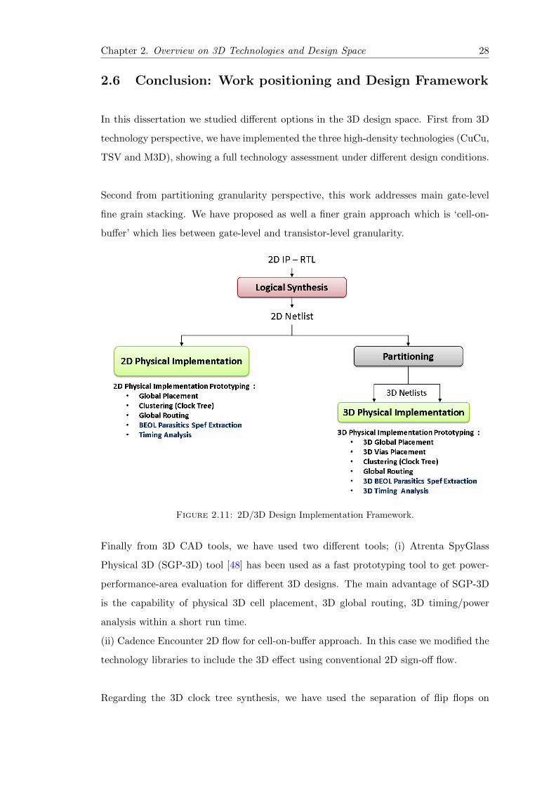
buffer’ which lies between gate-level and transistor-level granularity.
Figure 2.11: 2D/3D Design Implementation Framework.
Finally from 3D CAD tools, we have used two different tools; (i) Atrenta SpyGlass
Physical 3D (SGP-3D) tool [48] has been used as a fast prototyping tool to get power-
performance-area evaluation for different 3D designs. The main advantage of SGP-3D
is the capability of physical 3D cell placement, 3D global routing, 3D timing/power
analysis within a short run time.
(ii) Cadence Encounter 2D flow for cell-on-buffer approach. In this case we modified the
technology libraries to include the 3D effect using conventional 2D sign-off flow.
Regarding the 3D clock tree synthesis, we have used the separation of flip flops on

Chapter 2. Overview on 3D Technologies and Design Space 29
one tier using our proposed partitioning algorithm as we will discuss later.
Figure 2.11 shows the general 2D/3D design framework starting from the IP RTL, then
logic synthesis using Cadence RTL compiler, then 2D and 3D physical implementation
using SGP prototyping tool to get full evaluation on a power-performance-area metrics.
This design flow has been used in Chapters 4, 5 and 6.
Chapter 3
Cell-on-Buffer: A New Design
Approach for Monolithic 3D
3.1 Introduction
Stacking granularity varies depending on 3D technology used. As discussed in chapter
2, granularity spectrum starts from coarse-grain core-level stacking down to fine-grain
transistor-level stacking, where our focus in this work is the fine-grain partitioning thanks
to capabilites of high-density 3D technologies.
In this chapter we introduce a 3D Cell-on-Buffer (3DCoB) approach. 3DCoB consists in
splitting non-minimum drive standard cells into two stages: (i) a logic stage and (ii) a
buffering stage. The logic stage is being implemented by its equivalent minimum-drive
cell, while the buffering stage is implemented by a driving buffer with the same drive
as the original cell. The min-drive cell and the driving buffer is then stacked vertically.
Using this approach, the minimum-drive logic cell provides the same logical function as
the original cell, while the driving buffer guarantees the same driving capability.
3DCoB approach can be considered as a subset of Cell-on-Cell approach as it uses
the 2D cells and no need to redesign the standard cells. Additionally, 3DCoB provides
advantages for performance improvement thanks to decreased input gate capacitances,
no need to clock synchronization between the two tiers as well as partitioning step. As
30
Chapter 3. Cell-on-Buffer: A new design approach for Monolithic 3D 31
a result, full compatibility with conventional 2D digital implementation tools is kept.
Moreover, 3DCoB provides a separation between logic functionality and driving capa-
bilities, which can be used to introduce power optimization techniques as we will discuss
in section 3.5.
Consequently the 3DCoB approach provides:
i. Overall performance improvement.
ii. Full compatibility with the conventional sign-off physical implementation flow.
iii. No clock synchronization issue between the two tiers.
iv. No inter-tier routing metal layers between bottom cells.
v. Separation between logic functionality and driving capabilities.
Table 3.1 summarizes the differences between transistor-level, cell-on-cell and the pro-
posed cell-on-buffer approaches.
Table 3.1: Comparison between transistor-level (N/P), Cell-on-Buffer and Cell-on-Cell approaches for M3D technology
N/P Cell-on-Buffer Cell-on-Cell
Using 2D standard cells No Yes Yes
Using inter-tier routingmetal layers
No No No
2D Design flow compat-ibility
Yes Yes No
Usage of inter-tier VIAs In every cell Only in 3D cells Between cells (if req.)
In the following sections the full design flow, implementation and results for 3DCoB
approach are presented. Afterwards, a low-power approach is introduced using Multi-
VDD 3DCoB, with a full design flow.
Chapter 3. Cell-on-Buffer: A new design approach for Monolithic 3D 32
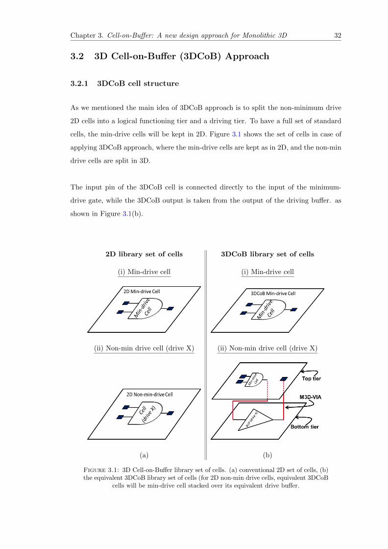
3.2 3D Cell-on-Buffer (3DCoB) Approach
3.2.1 3DCoB cell structure
As we mentioned the main idea of 3DCoB approach is to split the non-minimum drive
2D cells into a logical functioning tier and a driving tier. To have a full set of standard
cells, the min-drive cells will be kept in 2D. Figure 3.1 shows the set of cells in case of
applying 3DCoB approach, where the min-drive cells are kept as in 2D, and the non-min
drive cells are split in 3D.
The input pin of the 3DCoB cell is connected directly to the input of the minimum-
drive gate, while the 3DCoB output is taken from the output of the driving buffer. as
shown in Figure 3.1(b).
2D library set of cells 3DCoB library set of cells
(i) Min-drive cell (i) Min-drive cell
(ii) Non-min drive cell (drive X) (ii) Non-min drive cell (drive X)
(a) (b)
Figure 3.1: 3D Cell-on-Buffer library set of cells. (a) conventional 2D set of cells, (b)the equivalent 3DCoB library set of cells (for 2D non-min drive cells, equivalent 3DCoB
cells will be min-drive cell stacked over its equivalent drive buffer.
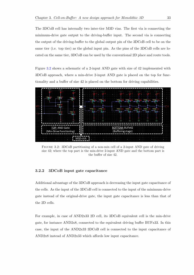
Chapter 3. Cell-on-Buffer: A new design approach for Monolithic 3D 33
The 3DCoB cell has internally two inter-tier M3D vias. The first via is connecting the
minimum-drive gate output to the driving-buffer input. The second via is connecting
the output of the driving-buffer to the global output pin of the 3DCoB cell to be on the
same tier (i.e. top tier) as the global input pin. As the pins of the 3DCoB cells are lo-
cated on the same tier, 3DCoB can be used by the conventional 2D place and route tools.
Figure 3.2 shows a schematic of a 2-input AND gate with size of 42 implemented with
3DCoB approach, where a min-drive 2-input AND gate is placed on the top for func-
tionality and a buffer of size 42 is placed on the bottom for driving capabilities.
Figure 3.2: 3DCoB partitioning of a non-min cell of a 2-input AND gate of drivingsize 42; where the top part is the min-drive 2-input AND gate and the bottom part is
the buffer of size 42.
3.2.2 3DCoB input gate capacitance
Additional advantage of the 3DCoB approach is decreasing the input gate capacitance of
the cells. As the input of the 3DCoB cell is connected to the input of the minimum-drive
gate instead of the original-drive gate, the input gate capacitance is less than that of
the 2D cells.
For example, in case of AND2x33 2D cell, its 3DCoB equivalent cell is the min-drive
gate, for instance AND2x8, connected to the equivalent driving buffer BUFx33. In this
case, the input of the AND2x33 3DCoB cell is connected to the input capacitance of
AND2x8 instead of AND2x33 which affords low input capacitance.
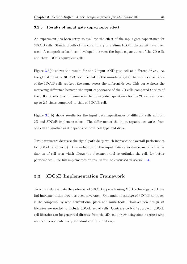
Chapter 3. Cell-on-Buffer: A new design approach for Monolithic 3D 34
3.2.3 Results of input gate capacitance effect
An experiment has been setup to evaluate the effect of the input gate capacitance for
3DCoB cells. Standard cells of the core library of a 28nm FDSOI design kit have been
used. A comparison has been developed between the input capacitance of the 2D cells
and their 3DCoB equivalent cells.
Figure 3.3(a) shows the results for the 2-input AND gate cell at different drives. As
the global input of 3DCoB is connected to the min-drive gate, the input capacitance
of the 3DCoB cells are kept the same across the different drives. This curve shows the
increasing difference between the input capacitance of the 2D cells compared to that of
the 3DCoB cells. Such difference in the input gate capacitance for the 2D cell can reach
up to 2.5 times compared to that of 3DCoB cell.
Figure 3.3(b) shows results for the input gate capacitances of different cells at both
2D and 3DCoB implementations. The difference of the input capacitance varies from
one cell to another as it depends on both cell type and drive.
Two parameters decrease the signal path delay which increases the overall performance
for 3DCoB approach (i) this reduction of the input gate capacitance and (ii) the re-
duction of cell area which allows the placement tool to optimize the cells for better
performance. The full implementation results will be discussed in section 3.4.
3.3 3DCoB Implementation Framework
To accurately evaluate the potential of 3DCoB approach using M3D technology, a 3D dig-
ital implementation flow has been developed. One main advantage of 3DCoB approach
is the compatibility with conventional place and route tools. However new design kit
libraries are needed to include 3DCoB set of cells. Contrary to N/P approach, 3DCoB
cell libraries can be generated directly from the 2D cell library using simple scripts with
no need to re-create every standard cell in the library.
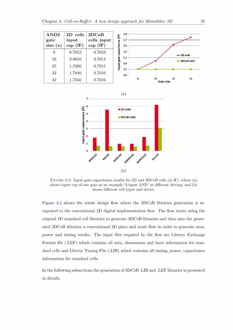
Chapter 3. Cell-on-Buffer: A new design approach for Monolithic 3D 35
AND2gatesize (x)
2D cellsinputcap (fF)
3DCoBcells inputcap (fF)
8 0.7053 0.7053
16 0.9858 0.7014
25 1.5380 0.7015
33 1.7840 0.7016
42 1.7350 0.7016
(a)
(b)
Figure 3.3: Input gate capacitance results for 2D and 3DCoB cells (in fF), where (a)shows input cap of one gate as an example ‘2-input AND’ at different driving, and (b)
shows different cell types and drives.
Figure 3.4 shows the whole design flow where the 3DCoB libraries generation is in-
tegrated to the conventional 2D digital implementation flow. The flow starts using the
original 2D standard cell libraries to generate 3DCoB libraries and then uses the gener-
ated 3DCoB libraries a conventional 2D place and route flow in order to generate area,
power and timing results. The input files required by the flow are Library Exchange
Format file (.LEF) which contains all area, dimensions and layer information for stan-
dard cells and Liberty Timing File (.LIB) which contains all timing, power, capacitance
information for standard cells.
In the following subsections the generation of 3DCoB .LIB and .LEF libraries is presented
in details.
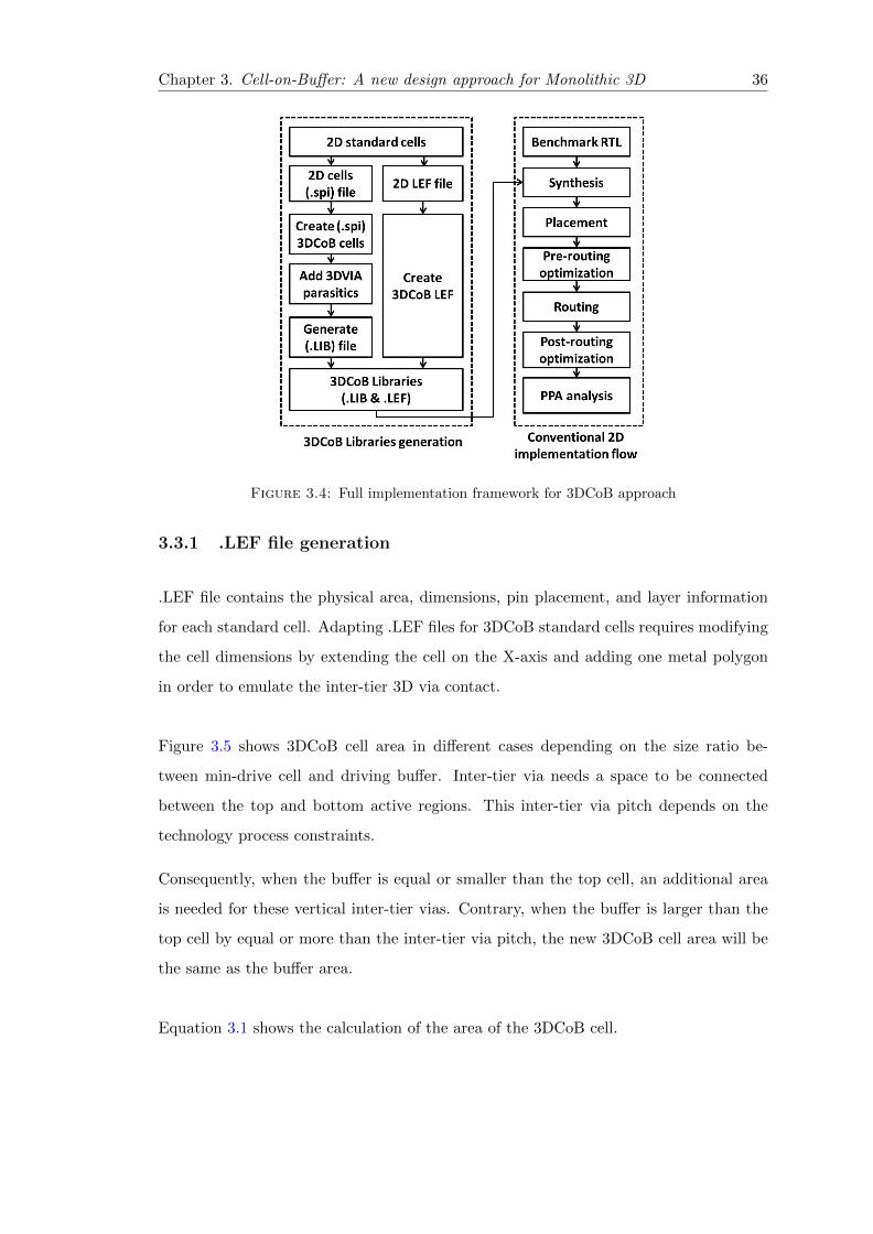
Chapter 3. Cell-on-Buffer: A new design approach for Monolithic 3D 36
Figure 3.4: Full implementation framework for 3DCoB approach
3.3.1 .LEF file generation
.LEF file contains the physical area, dimensions, pin placement, and layer information
for each standard cell. Adapting .LEF files for 3DCoB standard cells requires modifying
the cell dimensions by extending the cell on the X-axis and adding one metal polygon
in order to emulate the inter-tier 3D via contact.
Figure 3.5 shows 3DCoB cell area in different cases depending on the size ratio be-
tween min-drive cell and driving buffer. Inter-tier via needs a space to be connected
between the top and bottom active regions. This inter-tier via pitch depends on the
technology process constraints.
Consequently, when the buffer is equal or smaller than the top cell, an additional area
is needed for these vertical inter-tier vias. Contrary, when the buffer is larger than the
top cell by equal or more than the inter-tier via pitch, the new 3DCoB cell area will be
the same as the buffer area.
Equation 3.1 shows the calculation of the area of the 3DCoB cell.
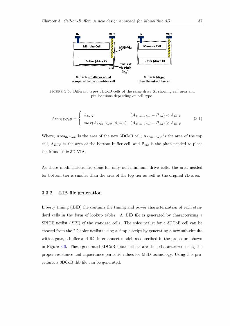
Chapter 3. Cell-on-Buffer: A new design approach for Monolithic 3D 37
Figure 3.5: Different types 3DCoB cells of the same drive X, showing cell area andpin locations depending on cell type.
Area3DCoB =
ABUF (AMin−Cell + Pvia) < ABUF
max(AMin−Cell, ABUF ) (AMin−Cell + Pvia) ≥ ABUF(3.1)
Where, Area3DCoB is the area of the new 3DCoB cell, AMin−Cell is the area of the top
cell, ABUF is the area of the bottom buffer cell, and Pvia is the pitch needed to place
the Monolithic 3D VIA.
As these modifications are done for only non-minimum drive cells, the area needed
for bottom tier is smaller than the area of the top tier as well as the original 2D area.
3.3.2 .LIB file generation
Liberty timing (.LIB) file contains the timing and power characterization of each stan-
dard cells in the form of lookup tables. A .LIB file is generated by characterizing a
SPICE netlist (.SPI) of the standard cells. The spice netlist for a 3DCoB cell can be
created from the 2D spice netlists using a simple script by generating a new sub-circuits
with a gate, a buffer and RC interconnect model, as described in the procedure shown
in Figure 3.6. These generated 3DCoB spice netlists are then characterized using the
proper resistance and capacitance parasitic values for M3D technology. Using this pro-
cedure, a 3DCoB .lib file can be generated.
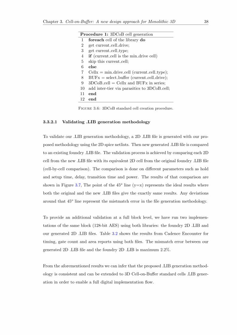
Chapter 3. Cell-on-Buffer: A new design approach for Monolithic 3D 38
Procedure 1: 3DCoB cell generation
1 foreach cell of the library do2 get current cell drive;3 get current cell type;4 if (current cell is the min drive cell)5 skip this current cell;6 else7 Cellx = min drive cell (current cell type);8 BUFx = select buffer (current cell drive);9 3DCoB cell = Cellx and BUFx in series;10 add inter-tier via parasitics to 3DCoB cell;11 end12 end
Figure 3.6: 3DCoB standard cell creation procedure.
3.3.2.1 Validating .LIB generation methodology
To validate our .LIB generation methodology, a 2D .LIB file is generated with our pro-
posed methodology using the 2D spice netlists. Then new generated .LIB file is compared
to an existing foundry .LIB file. The validation process is achieved by comparing each 2D
cell from the new .LIB file with its equivalent 2D cell from the original foundry .LIB file
(cell-by-cell comparison). The comparison is done on different parameters such as hold
and setup time, delay, transition time and power. The results of that comparison are
shown in Figure 3.7, The point of the 45o line (y=x) represents the ideal results where
both the original and the new .LIB files give the exactly same results. Any deviations
around that 45o line represent the mistmatch error in the file generation methodology.
To provide an additional validation at a full block level, we have run two implemen-
tations of the same block (128-bit AES) using both libraries: the foundry 2D .LIB and
our generated 2D .LIB files. Table 3.2 shows the results from Cadence Encounter for
timing, gate count and area reports using both files. The mismatch error between our
generated 2D .LIB file and the foundry 2D .LIB is maximum 2.2%.
From the aforementioned results we can infer that the proposed .LIB generation method-
ology is consistent and can be extended to 3D Cell-on-Buffer standard cells .LIB gener-
ation in order to enable a full digital implementation flow.
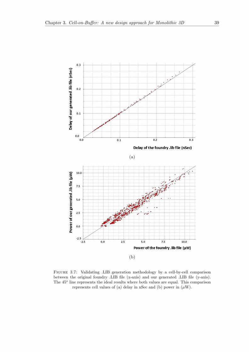
Chapter 3. Cell-on-Buffer: A new design approach for Monolithic 3D 39
(a)
(b)
Figure 3.7: Validating .LIB generation methodology by a cell-by-cell comparisonbetween the original foundry .LIB file (x-axis) and our generated .LIB file (y-axis).The 45o line represents the ideal results where both values are equal. This comparison
represents cell values of (a) delay in nSec and (b) power in (µW).
Chapter 3. Cell-on-Buffer: A new design approach for Monolithic 3D 40
Table 3.2: Validating .LIB generation methodology with a full block implementation.A comparison of implementation results of 128-bit AES block using both .LIB files: the
original foundry .LIB file and our generated .LIB file
FoundryLibraries
GeneratedLibraries
MismatchError
Timing slack 0 ps 0 ps 0%
No. of cells 130086 129113 0.75%
No. of FlipFlops 5568 5568 0%
No. of INVs 10973 11091 +1.1%
No. of Buffers 91 93 +2.2%
No. of Logic gates 113454 112361 -1.0%
Cell Area 99860 99562 -0.3%
3.4 3DCoB Performance-Power Results
To evaluate the proposed approach, selected benchmark blocks are implemented in 2D
and 3DCoB using 28nm FDSOI technology and Monolithic 3D integration technology
demonstrated in [8]. We used a sign-off physical implementation flow using CADENCE
Encounter place and route tool. The 3DCoB libraries are generated as shown in Fig-
ure 3.4. We select a set of growing complexity benchmark blocks consists of: openMSP,
Fast Fourier Transform (FFT) and 128-bit Advanced Encryption System (AES) decoder.
Table 3.3 summarizes the physical implementation results for the openMSP, FFT and
AES blocks at different target clock frequency. The performance is measured as the
effective clock frequency (the target clock period without the slack time). The power
results are obtained from the place and route power reports, and then they are scaled to
the max performance frequency for fairly comparison. The results are obtained at the
same footprint area for each block.
At the same target frequency, 3DCoB approach improves performances by 20.5% and
9.6% compared to 2D for the AES (at 2.5GHz) and FFT (at 1.67GHz) blocks, respec-
tively. OpenMSP block shows no gain in performances due to its small size and low
number of standard cells.
To show the maximum achievable frequency at the same block area, we vary the target
clock frequency of each block till reach the max performance point that can be achieved.
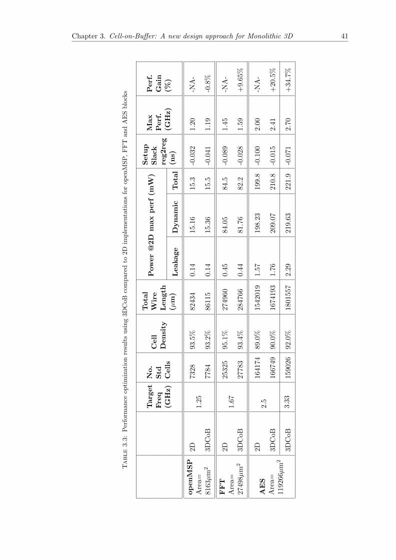
Chapter 3. Cell-on-Buffer: A new design approach for Monolithic 3D 41
Table3.3:
Per
form
ance
opti
miz
atio
nre
sult
su
sin
g3D
CoB
com
pare
dto
2D
imp
lem
enta
tion
sfo
rop
enM
SP
,F
FT
an
dA
ES
blo
cks
Targ
et
Fre
q(G
Hz)
No.
Std
Cells
Cell
Den
sity
Tota
lW
ire
Len
gth
(µm
)
Pow
er
@2D
max
perf
(mW
)S
etu
pS
lack
reg2re
g(n
s)
Max
Perf
.(G
Hz)
Perf
.G
ain
(%)
Leakage
Dyn
am
icT
ota
l
op
en
MS
PA
rea=
816
3µm
2
2D
1.25
7328
93.5
%82
434
0.14
15.1
615
.3-0
.032
1.20
-NA
-
3D
CoB
7784
93.2
%86
115
0.14
15.3
615
.5-0
.041
1.19
-0.8
%
FF
TA
rea=
274
98µ
m2
2D
1.67
2532
595
.1%
2749
600.
4584
.05
84.5
-0.0
891.
45-N
A-
3D
CoB
2778
393
.4%
2847
660.
4481
.76
82.2
-0.0
281.
59+
9.65
%
AE
SA
rea=
119
266µ
m2
2D
2.5
1641
7489
.0%
1542
019
1.57
198.
2319
9.8
-0.1
002.
00-N
A-
3D
CoB
1667
4990
.0%
1674
193
1.76
209.
0721
0.8
-0.0
152.
41+
20.5
%
3D
CoB
3.33
1590
2692
.0%
1801
557
2.29
219.
6322
1.9
-0.0
712.
70+
34.7
%
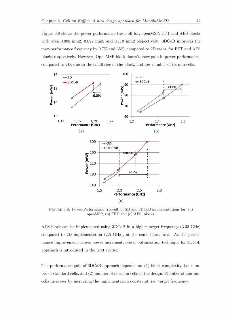
Chapter 3. Cell-on-Buffer: A new design approach for Monolithic 3D 42
Figure 3.8 shows the power-performance trade-off for, openMSP, FFT and AES blocks
with area 0.008 mm2, 0.027 mm2 and 0.119 mm2 respectively. 3DCoB improves the
max-performance frequency by 9.7% and 35%, compared to 2D cases, for FFT and AES
blocks respectively. However, OpenMSP block doesn’t show gain in power-performance,
compared to 2D, due to the small size of the block, and low number of its min-cells.
(a) (b)
(c)
Figure 3.8: Power-Performance tradeoff for 2D and 3DCoB implementations for: (a)openMSP, (b) FFT and (c) AES, blocks.
AES block can be implemented using 3DCoB in a higher target frequency (3.33 GHz)
compared to 2D implementation (2.5 GHz), at the same block area. As the perfor-
mance improvement causes power increment, power optimization technique for 3DCoB
approach is introduced in the next section.
The performance gain of 3DCoB approach depends on: (1) block complexity, i.e. num-
ber of standard cells, and (2) number of non-min cells in the design. Number of non-min
cells increases by increasing the implementation constraint, i.e. target frequency.
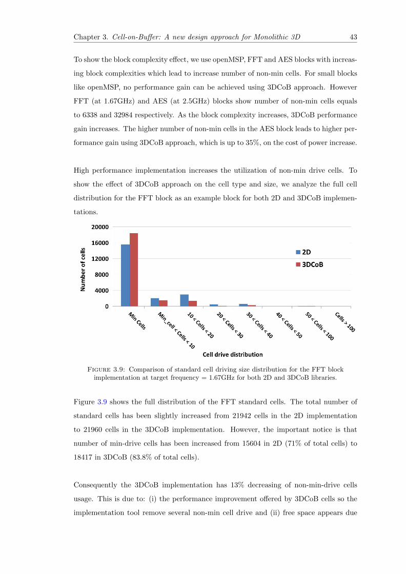
Chapter 3. Cell-on-Buffer: A new design approach for Monolithic 3D 43
To show the block complexity effect, we use openMSP, FFT and AES blocks with increas-
ing block complexities which lead to increase number of non-min cells. For small blocks
like openMSP, no performance gain can be achieved using 3DCoB approach. However
FFT (at 1.67GHz) and AES (at 2.5GHz) blocks show number of non-min cells equals
to 6338 and 32984 respectively. As the block complexity increases, 3DCoB performance
gain increases. The higher number of non-min cells in the AES block leads to higher per-
formance gain using 3DCoB approach, which is up to 35%, on the cost of power increase.
High performance implementation increases the utilization of non-min drive cells. To
show the effect of 3DCoB approach on the cell type and size, we analyze the full cell
distribution for the FFT block as an example block for both 2D and 3DCoB implemen-
tations.
Figure 3.9: Comparison of standard cell driving size distribution for the FFT blockimplementation at target frequency = 1.67GHz for both 2D and 3DCoB libraries.
Figure 3.9 shows the full distribution of the FFT standard cells. The total number of
standard cells has been slightly increased from 21942 cells in the 2D implementation
to 21960 cells in the 3DCoB implementation. However, the important notice is that
number of min-drive cells has been increased from 15604 in 2D (71% of total cells) to
18417 in 3DCoB (83.8% of total cells).
Consequently the 3DCoB implementation has 13% decreasing of non-min-drive cells
usage. This is due to: (i) the performance improvement offered by 3DCoB cells so the
implementation tool remove several non-min cell drive and (ii) free space appears due
Chapter 3. Cell-on-Buffer: A new design approach for Monolithic 3D 44
to 3D stacking area reduction which allows the tool to insert more buffers on the critical
paths to reach higher performances.
3.5 Low-Power Multi-VDD CoB (MV-CoB) Approach
Different low-power techniques have been developed such as Digital Voltage and Fre-
quency Scaling (DVFS) and VDD-Hoping [49, 50]. To apply power optimization for
3DCoB approach, multiple-VDD has been used as a low power technique. In this sec-
tion we introduce a new methodology to develop a low-power Multiple-VDD 3DCoB
(MV-3DCoB) approach.
One of the main advantages of the 3DCoB is separating the driving capabilities from the
logic functionality. Our multi-VDD 3DCoB methodology aims to decrease the supply
voltage only for the logic functionality and keep the original supply voltage for the driv-
ing buffers. By this way, the driving capability of the multi-VDD 3DCoB cells is kept
the same as the original single-VDD 3DCoB cells. Consequently, the power consumption
decreases without much degradation of the performance.
For example, if the single-VDD cells with a supply of ‘VDD’, the multi-VDD 3DCoB
cells will have a top voltage supply equals to ‘β *VDD’ for the logic functionality where
(β less than 1) and a bottom voltage supply equals to ‘VDD’ for driving buffer.
Figure 3.10 shows the different connectivity for 3DCoB where; the first scheme is con-
necting two min-drive cells directly, the second scheme is the inter-cell connection be-
tween the min-drive gate and its driving buffer, the third signals are connecting the
outputs of the driving buffers and the inputs of the next min-drive gates.
Using these different connectivity schemes, the MV-3DCoB power consumption can be
estimated as shown in equation 3.2:
PMultiV DD = α ∗ f ∗ V 2DD[β2(CgminNmin + CgBUFNnon−min) + CgminNnon−min] (3.2)
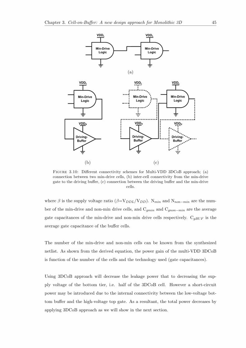
Chapter 3. Cell-on-Buffer: A new design approach for Monolithic 3D 45
(a)
(b) (c)
Figure 3.10: Different connectivity schemes for Multi-VDD 3DCoB approach; (a)connection between two min-drive cells, (b) inter-cell connectivity from the min-drivegate to the driving buffer, (c) connection between the driving buffer and the min-drive
cells.
where β is the supply voltage ratio (β=VDDL/VDD). Nmin and Nnon−min are the num-
ber of the min-drive and non-min drive cells, and Cgmin and Cgnon−min are the average
gate capacitances of the min-drive and non-min drive cells respectively. CgBUF is the
average gate capacitance of the buffer cells.
The number of the min-drive and non-min cells can be known from the synthesized
netlist. As shown from the derived equation, the power gain of the multi-VDD 3DCoB
is function of the number of the cells and the technology used (gate capacitances).
Using 3DCoB approach will decrease the leakage power that to decreasing the sup-
ply voltage of the bottom tier, i.e. half of the 3DCoB cell. However a short-circuit
power may be introduced due to the internal connectivity between the low-voltage bot-
tom buffer and the high-voltage top gate. As a resultant, the total power decreases by
applying 3DCoB approach as we will show in the next section.
Chapter 3. Cell-on-Buffer: A new design approach for Monolithic 3D 46
Creating a Power Distribution Network (PDN) is an important phase for 3D design
flow. Using M3D technology, PDN can create more routing obstruction on the bottom
tier due to the vias connected the top PDN network with the bottom one. One way is
by implementing level shifters or DC-DC converters, such as Digital Low-Drop-Out (D-
LDO) or switched capacitor voltage regulator, to lower the voltage supply. As 3DCoB
approach converts only the non-min drive cells, the bottom tier is not fully occupied and
has free silicon space. Such free space depends on the ratio between number of min-drive
cells and the non-min drive cells.
Another way is by controlling the number of M3D vias used for PDN connections. The
parasitics of these M3D vias control the voltage drop and the current supply required
at the bottom tier. The number of M3D vias used for PDN connections is determined
according to the current required for the bottom tier.
3.6 Power Optimization Results MV-CoB Performance-
Power-Area Results
To fully implement the Multi-VDD 3DCoB (MV-3DCoB) approach, we use the same
design flow methodology introduced in section 3.3. MV-3DCoB cells are re-characterized
to include the effect of decreasing the top voltage supply on both delay and power of
the cells. The MV-3DCoB .LIB and .LEF files are generated and used in a full place
and route flow using 28nm FDSOI technology. The top-tier functioning supply voltage
(VDDL) is set to 0.9V, while the bottom-tier buffering supply voltage (VDDH) is set to
1V.
Table 3.4 summarizes the MV-3DCoB results compared to: (i) 2D and (ii) single-VDD
3DCoB implementations. The supply voltage in both 2D and single-VDD 3DCoB cases
is set to 1V. To achieve a faire comparison, the same set of benchmarks is implemented
using the same design frame work as 2D and single-VDD 3DCoB.
In case of AES block at 1.42GHz target frequency, MV-3DCoB reduces power by 21.8%
with only performance reduction of 2% compared to 2D. For the FFT block at 1.25GHz,
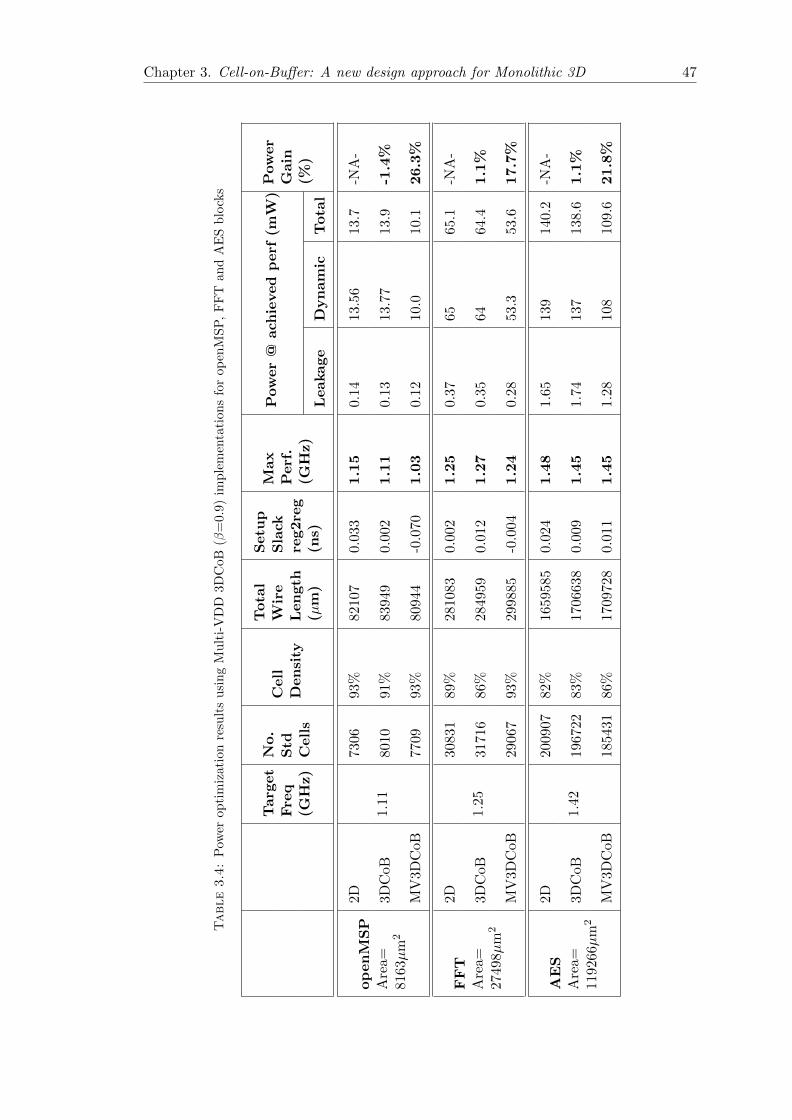
Chapter 3. Cell-on-Buffer: A new design approach for Monolithic 3D 47
Table3.4:
Pow
erop
tim
izat
ion
resu
lts
usi
ng
Mu
lti-
VD
D3D
CoB
(β=
0.9
)im
ple
men
tati
on
sfo
rop
enM
SP
,F
FT
an
dA
ES
blo
cks
Targ
et
Fre
q(G
Hz)
No.
Std
Cells
Cell
Den
sity
Tota
lW
ire
Len
gth
(µm
)
Setu
pS
lack
reg2re
g(n
s)
Max
Perf
.(G
Hz)
Pow
er
@ach
ieved
perf
(mW
)P
ow
er
Gain
(%)
Leakage
Dyn
am
icT
ota
l
op
en
MS
PA
rea=
816
3µm
2
2D
1.11
7306
93%
8210
70.
033
1.1
50.
1413
.56
13.7
-NA
-
3D
CoB
8010
91%
8394
90.
002
1.1
10.
1313
.77
13.9
-1.4
%
MV
3D
CoB
7709
93%
8094
4-0
.070
1.0
30.
1210
.010
.126.3
%
FF
TA
rea=
274
98µ
m2
2D
1.25
3083
189
%28
1083
0.00
21.2
50.
3765
65.1
-NA
-
3D
CoB
3171
686
%28
4959
0.01
21.2
70.
3564
64.4
1.1
%
MV
3D
CoB
2906
793
%29
9885
-0.0
041.2
40.
2853
.353
.617.7
%
AE
SA
rea=
119
266µ
m2
2D
1.42
2009
0782
%16
5958
50.
024
1.4
81.
6513
914
0.2
-NA
-
3D
CoB
1967
2283
%17
0663
80.
009
1.4
51.
7413
713
8.6
1.1
%
MV
3D
CoB
1854
3186
%17
0972
80.
011
1.4
51.
2810
810
9.6
21.8
%
Chapter 3. Cell-on-Buffer: A new design approach for Monolithic 3D 48
MV-3DCoB reduces power by 17.7% with only performance degradation by 0.8% com-
pared to 2D. However, in case of openMSP block at 1.11GHz, MV-3DCoB reduces power
by 26.3% but with performance degradation of 10.4% compared to 2D. This is due to
the small size effect of the block.
Figure 3.11 shows the power-performance results for the benchmark circuits. As shown,
MV-3DCoB provides lower power compared to both 2D and 3DCoB implementations
by 26%, 18% and 22% for openMSP, FFT and AES blocks respectively.
For the leakage power, decreasing the top-tier supply voltage in the Multi-VDD 3DCoB
decreases the leakage compared to the original 2D design. For example, in case of FFT
(with 1.25GHz target clock frequency), the leakage power for the 2D equals 0.37mW
while for the MV-3DCoB equals 0.28mW, as shown in Table 3.4. As shown, MV-3DCoB
power gain depends on the number of non-min cells in the design which increases by
increasing block complexity, or by changing the constraints applied in the place and
route tool such as increasing target clock frequency.
3.7 Summary and Conclusion
In this chapter we propose 3D Cell-on-Buffer (3DCoB) as a design approach for M3D.
The main idea for 3DCoB is to split the conventional 2D cells into two stages; logical
stage (min-drive cells) and driving stage (same-drive buffer). The logical cell is stacked
over the driving buffer using the advantage of the M3D technology. The implementation
results show up to 35% performance improvement of 3DCoB compared to the same 2D
design. The performance gain highly depends on the block complexity and architecture.
Taking the advantage of logic and buffering separation, we presented Multi-VDD 3DCoB
(MV-3DCoB) as a power optimization technique to the 3DCoB. For MV-3DCoB, the
min-drive logic gates have a low supply voltage while the driving buffers have the nor-
mal supply voltage to maintain the original driving capability. The implementation
results using MV-3DCoB cells show power gain of 21.8% compared to the 2D results
on the cost of 2% performance degradation for the AES block at the same footprint area.
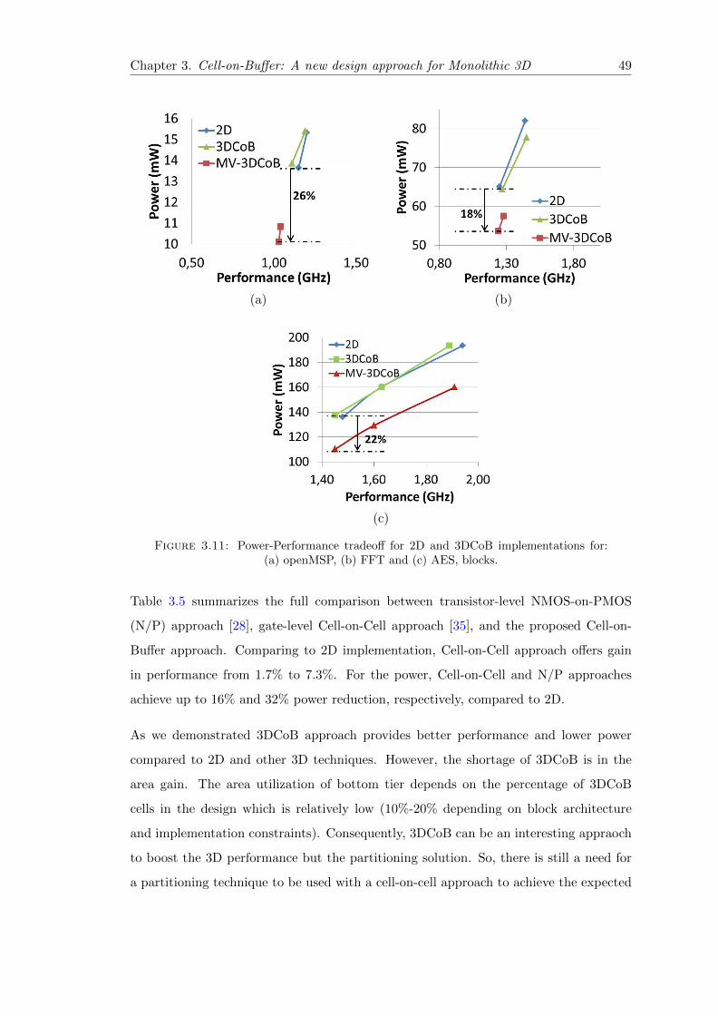
Chapter 3. Cell-on-Buffer: A new design approach for Monolithic 3D 49
(a) (b)
(c)
Figure 3.11: Power-Performance tradeoff for 2D and 3DCoB implementations for:(a) openMSP, (b) FFT and (c) AES, blocks.
Table 3.5 summarizes the full comparison between transistor-level NMOS-on-PMOS
(N/P) approach [28], gate-level Cell-on-Cell approach [35], and the proposed Cell-on-
Buffer approach. Comparing to 2D implementation, Cell-on-Cell approach offers gain
in performance from 1.7% to 7.3%. For the power, Cell-on-Cell and N/P approaches
achieve up to 16% and 32% power reduction, respectively, compared to 2D.
As we demonstrated 3DCoB approach provides better performance and lower power
compared to 2D and other 3D techniques. However, the shortage of 3DCoB is in the
area gain. The area utilization of bottom tier depends on the percentage of 3DCoB
cells in the design which is relatively low (10%-20% depending on block architecture
and implementation constraints). Consequently, 3DCoB can be an interesting appraoch
to boost the 3D performance but the partitioning solution. So, there is still a need for
a partitioning technique to be used with a cell-on-cell approach to achieve the expected
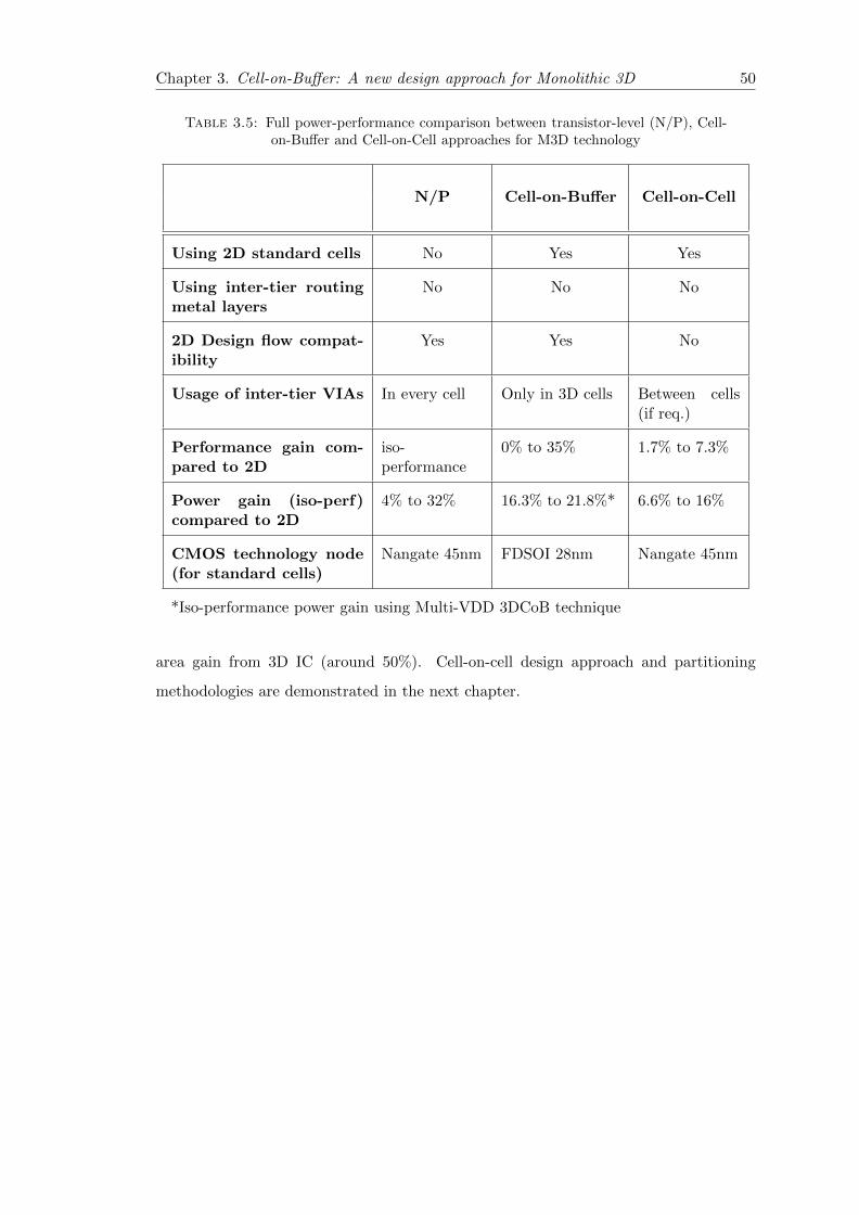
Chapter 3. Cell-on-Buffer: A new design approach for Monolithic 3D 50
Table 3.5: Full power-performance comparison between transistor-level (N/P), Cell-on-Buffer and Cell-on-Cell approaches for M3D technology
N/P Cell-on-Buffer Cell-on-Cell
Using 2D standard cells No Yes Yes
Using inter-tier routingmetal layers
No No No
2D Design flow compat-ibility
Yes Yes No
Usage of inter-tier VIAs In every cell Only in 3D cells Between cells(if req.)
Performance gain com-pared to 2D
iso-performance
0% to 35% 1.7% to 7.3%
Power gain (iso-perf)compared to 2D
4% to 32% 16.3% to 21.8%* 6.6% to 16%
CMOS technology node(for standard cells)
Nangate 45nm FDSOI 28nm Nangate 45nm
*Iso-performance power gain using Multi-VDD 3DCoB technique
area gain from 3D IC (around 50%). Cell-on-cell design approach and partitioning
methodologies are demonstrated in the next chapter.
Chapter 4
Gate-Level 3D Partitioning
4.1 Introduction: 3D Partitioning
Area gain is one of the main advantages of 3D technologies. In the previous chapter we
present a 3D cell-on-buffer approach which shows power and performance improvements.
However the need for gate-level cell-on-cell integration is crucial to achieve high area gain,
i.e. around 50%. Considering complex designs of several thousands to millions gates
(K-Gate to M-Gates) with high-density M3D technology offering up to 108vias/mm2 [8],
there is an important question is raising of how to distribute cells efficiently on top and
bottom tiers.
To create a 3D design, part of the circuit should be placed on one die and the other part
should be placed on a second die, that’s what we call “Partitioning”. Conventionally
for two-layers 3DIC, half of the design is assigned to one die and the another half is
assigned to the second die. The question is how to partition a 2D design to create a 3D
design.
Partitioning is the process to distribute logical cells of a design on different stacked
3D layers. This step is critical in the 3D design flow as it affects the power-performance-
area gain of the new 3D design. As 3D power-performance gains are achieved thanks
to cutting long wires to 3D connections (3D VIA), different partitioning techniques will
give different results due to the different wires have been cut. The ratio of RC parasitics
between a 3D VIA and the 2D wire is important to determine the power-performance
51
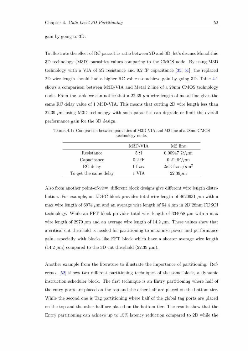
Chapter 4. Gate-Level 3D Partitioning 52
gain by going to 3D.
To illustrate the effect of RC parasitics ratio between 2D and 3D, let’s discuss Monolithic
3D technology (M3D) parasitics values comparing to the CMOS node. By using M3D
technology with a VIA of 5Ω resistance and 0.2 fF capacitance [35, 51], the replaced
2D wire length should had a higher RC values to achieve gain by going 3D. Table 4.1
shows a comparison between M3D-VIA and Metal 2 line of a 28nm CMOS technology
node. From the table we can notice that a 22.39 µm wire length of metal line gives the
same RC delay value of 1 M3D-VIA. This means that cutting 2D wire length less than
22.39 µm using M3D technology with such parasitics can degrade or limit the overall
performance gain for the 3D design.
Table 4.1: Comparison between parasitics of M3D-VIA and M2 line of a 28nm CMOStechnology node.
M3D-VIA M2 line
Resistance 5 Ω 0.00947 Ω/µm
Capacitance 0.2 fF 0.21 fF/µm
RC delay 1 f sec 2e-3 f sec/µm2
To get the same delay 1 VIA 22.39µm
Also from another point-of-view, different block designs give different wire length distri-
bution. For example, an LDPC block provides total wire length of 4620931 µm with a
max wire length of 6974 µm and an average wire length of 54.4 µm in 2D 28nm FDSOI
technology. While an FFT block provides total wire length of 334058 µm with a max
wire length of 2970 µm and an average wire length of 14.2 µm. These values show that
a critical cut threshold is needed for partitioning to maximize power and performance
gain, especially with blocks like FFT block which have a shorter average wire length
(14.2 µm) compared to the 3D cut threshold (22.39 µm).
Another example from the literature to illustrate the importance of partitioning. Ref-
erence [52] shows two different partitioning techniques of the same block, a dynamic
instruction scheduler block. The first technique is an Entry partitioning where half of
the entry ports are placed on the top and the other half are placed on the bottom tier.
While the second one is Tag partitioning where half of the global tag ports are placed
on the top and the other half are placed on the bottom tier. The results show that the
Entry partitioning can achieve up to 15% latency reduction compared to 2D while the
Chapter 4. Gate-Level 3D Partitioning 53
Tag partitioning can achieve up to only 3.4%.
From these results, we can emphasis that different partitioning of the same block under
the same technology parameters and the same implementation framework can achieve
different 3D power-performance results.
4.2 Previous Gate-Level Partitioning Techniques
As illustrated there are two main approaches for designing 3D blocks in the literature.
The first one is the architecture-level approach which takes long time that is not compat-
ible with complex and large-scale designs. The second approach consists in partitioning
the 2D netlist to get the 3D netlists using a partitioning algorithm which is gate-level
partitioning. In this chapter, we will focus on the gate-level partitioning.
Gate-level partitioning has two different approaches:
i. Min-cut partitioning technique.
In this technique the partitioning algorithm targets to minimize the number of 3D
contacts for a certain area ratio between top and bottom tiers, typically the balanced
(equal) area ratio.
ii. Performance-driven partitioning technique.
In this technique the partitioning algorithm targets to maximize the performance
gain of 3D regardless the number of 3D contacts.
A hyper-graph partitioning tool named ‘HMetis’ was presented in reference [25] as a
min-cut partitioning algorithm. Reference [26] demonstrates a 3D Digital Signal Pro-
cessor (DSP) with a gate-level partitioning using hMetis partitioning tool. In this case,
the hMetis tends to minimize number of 3D contacts with equal area ratio between top
and bottom tiers. Copper-to-Copper technology has been used in that work with a 5µm
pitch of 3D contacts.
However Monolithic 3D technology offers very high density 3D contacts with a pitch
scaled down to 0.11 µm for 28nm technology. This technology breaks the limitation in
Chapter 4. Gate-Level 3D Partitioning 54
terms of number of 3D connections which opens new paradigm of partitioning to im-
porve performance and power results.
In 2007, Cong et al [53] introduces the concept of Local Stacking Transformation (LST)
and it was fully explained in [46]. LST technique assume starting with an optimized 2D
placement then shrink placement area with K factor, where K is the number of stacked
layers. Then a legalized phase is performed to distribute bin the close cells and distribute
them on the different stacked dies. LST was introduced for TSV-based implementation.
Similarly, CELONCEL placer was introduced based on the same concept but for Mono-
lithic 3D technology [39]. CELONCEL shrinks all standard cells (deflating phase) then
doing the 2D placement optimization then 3D distribution of standard cells and finally
restoring the standard cell sizes (inflating phase).
Similar technique was used by Reference [27] as a placement-driven partitioning method-
ology for monolithic 3D technology with preserving the black boxes of the design.
Placement-drive partitioning technique starts either with initial 3D placement or 2D
optimized placement.
Although the first two techniques (LST[53] and CELONCEL[39]) are introduced as
3D placers but they are actually performing gate-level 3D partitioning. 3D placement
is how to place standard cells in 3D dimensions (x, y, z) instead of only two dimensions.
This process includes optimizing the cell placement vertically in z-direction which solves
the same problem as 3D standard cell partitioning (cell-on-cell).
4.3 Physical-Aware Partitioning (PAP) Methodology
Previous 3D partitioning techniques are constrained by minimizing number of 3D con-
tacts and targeting to achieve balanced area ratio between top and bottom tiers. These
techniques are achieved without taking into consideration performance of the obtained
partitioning design. Also as we are focusing on gate-level cell-on-cell partitioning, tens
of thousands of gates need to be assigned either on top or on bottom layer to achieve
the partitioning. Consequently an automated framework is needed to perform the whole
partitioning methodology for different blocks with a physical-aware parameters.
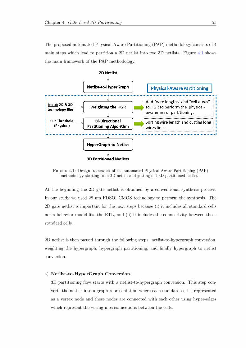
Chapter 4. Gate-Level 3D Partitioning 55
The proposed automated Physical-Aware Partitioning (PAP) methodology consists of 4
main steps which lead to partition a 2D netlist into two 3D netlists. Figure 4.1 shows
the main framework of the PAP methodology.
Figure 4.1: Design framework of the automated Physical-Aware-Partitioning (PAP)methodology starting from 2D netlist and getting out 3D partitioned netlists.
At the beginning the 2D gate netlist is obtained by a conventional synthesis process.
In our study we used 28 nm FDSOI CMOS technology to perform the synthesis. The
2D gate netlist is important for the next steps because (i) it includes all standard cells
not a behavior model like the RTL, and (ii) it includes the connectivity between those
standard cells.
2D netlist is then passed through the following steps: netlist-to-hypergraph conversion,
weighting the hypergraph, hypergraph partitioning, and finally hypergraph to netlist
conversion.
a) Netlist-to-HyperGraph Conversion.
3D partitioning flow starts with a netlist-to-hypergraph conversion. This step con-
verts the netlist into a graph representation where each standard cell is represented
as a vertex node and these nodes are connected with each other using hyper-edges
which represent the wiring interconnections between the cells.
Chapter 4. Gate-Level 3D Partitioning 56
Figure 4.2 shows an example of a gate netlist conversion to hyper-graph representa-
tion of a small circuit.
b) Weighting the HyperGraph.
The second step is weighting the hypergraph. HGR weighting is the procedure at
which every cell and wire takes a numerical value representing its weight in the par-
titioning algorithm. These numerical values represent the physical parameters of the
design.
Each standard cell is represented by its physical cell area to control the area ratio
between top and bottom die of the 3D design. While each interconnection is rep-
resented by its 2D wire length, so that the partitioning algorithm starts to cut the
longest wires first. The wire length values can be obtained using a wire length model,
such as the half-perimeter wire length (HPWL) model. These wire length values are
then used in the partitioning flow to arrange wiring interconnects from the longest
to the shortest one.
Weighting phase is important as it add the physical awareness to the netlist. The
HGR shown in Figure 4.2 includes an arbitrary weight values for both gates (vertices)
and wires (edges).
c) Partitioning Algorithm.
The third step is the partitioning algorithm. In this step, the core of partitioning is
performed at which the weighted HGR is partitioned into two (or more) HGRs. In
our study we used the min-cut hMetis tool as a reference partitioning algorithm and
we proposed a Bi-Directional Partitioning (BDP) algorithm to improve performance
and power of the 3D design.
As the BDP algorithm is the main core of the partitioning work flow, it will be
discussed in details in the following section (4.4).
d) HyperGraph-to-Netlist Conversion and Generate 3D Netlists.
The final step is a hyper-graph to netlist conversion. In this step the partitioned
HGRs are converted back to a gate netlist from which we can get two (or more)
netlists representing top and bottom layers. A further step is done using some scripts
to include the top and bottom netlists into one hierarchical netlist for the 3D design
where top and bottom netlists are internal modules.
This 3D netlist is then used in the implementation tool to perform the power-
performance-area analysis.
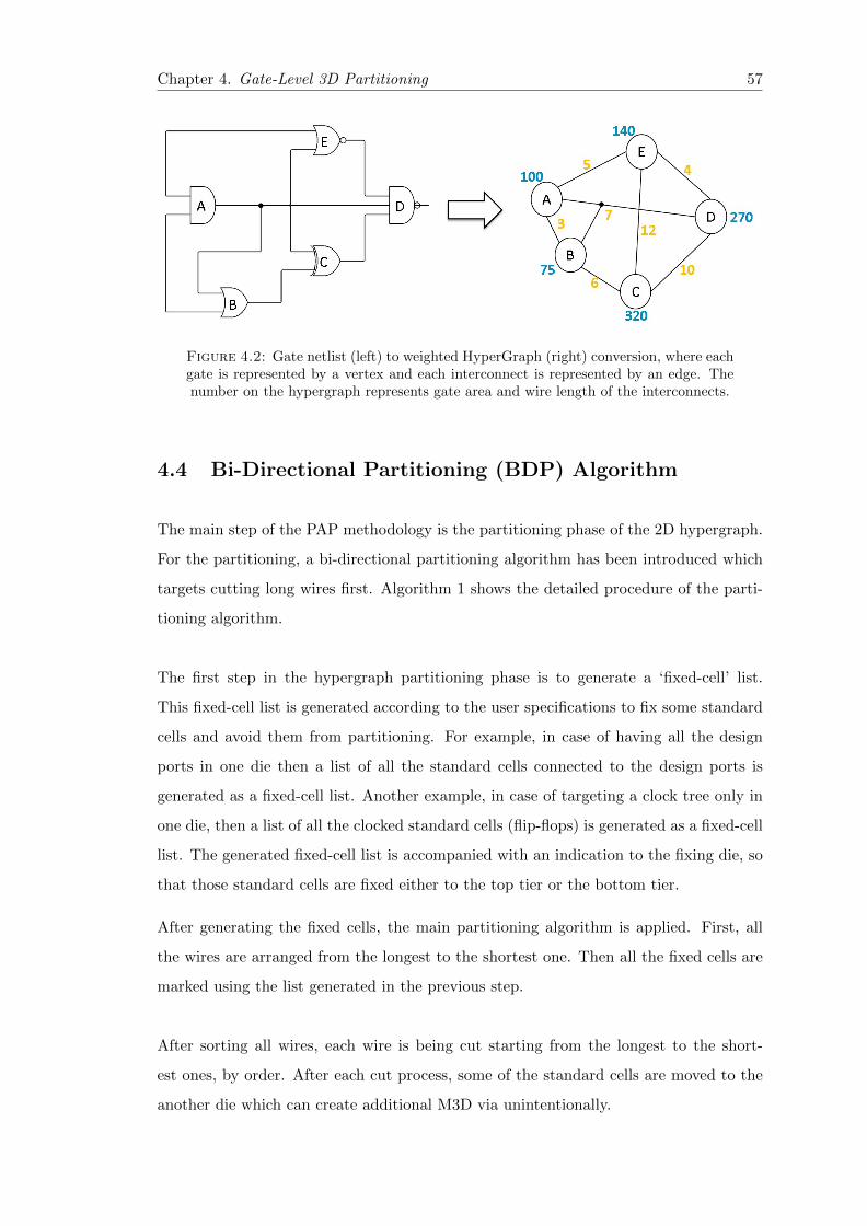
Chapter 4. Gate-Level 3D Partitioning 57
Figure 4.2: Gate netlist (left) to weighted HyperGraph (right) conversion, where eachgate is represented by a vertex and each interconnect is represented by an edge. Thenumber on the hypergraph represents gate area and wire length of the interconnects.
4.4 Bi-Directional Partitioning (BDP) Algorithm
The main step of the PAP methodology is the partitioning phase of the 2D hypergraph.
For the partitioning, a bi-directional partitioning algorithm has been introduced which
targets cutting long wires first. Algorithm 1 shows the detailed procedure of the parti-
tioning algorithm.
The first step in the hypergraph partitioning phase is to generate a ‘fixed-cell’ list.
This fixed-cell list is generated according to the user specifications to fix some standard
cells and avoid them from partitioning. For example, in case of having all the design
ports in one die then a list of all the standard cells connected to the design ports is
generated as a fixed-cell list. Another example, in case of targeting a clock tree only in
one die, then a list of all the clocked standard cells (flip-flops) is generated as a fixed-cell
list. The generated fixed-cell list is accompanied with an indication to the fixing die, so
that those standard cells are fixed either to the top tier or the bottom tier.
After generating the fixed cells, the main partitioning algorithm is applied. First, all
the wires are arranged from the longest to the shortest one. Then all the fixed cells are
marked using the list generated in the previous step.
After sorting all wires, each wire is being cut starting from the longest to the short-
est ones, by order. After each cut process, some of the standard cells are moved to the
another die which can create additional M3D via unintentionally.
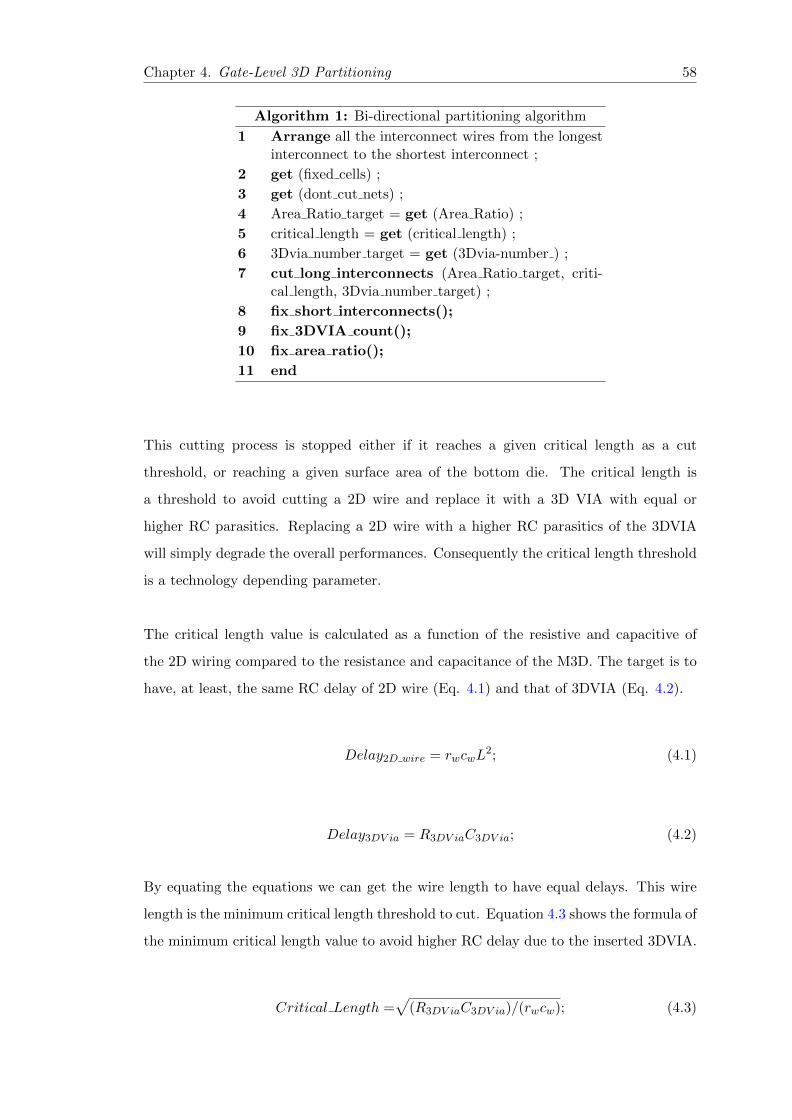
Chapter 4. Gate-Level 3D Partitioning 58
Algorithm 1: Bi-directional partitioning algorithm
1 Arrange all the interconnect wires from the longestinterconnect to the shortest interconnect ;
2 get (fixed cells) ;
3 get (dont cut nets) ;
4 Area Ratio target = get (Area Ratio) ;
5 critical length = get (critical length) ;
6 3Dvia number target = get (3Dvia-number ) ;
7 cut long interconnects (Area Ratio target, criti-cal length, 3Dvia number target) ;
8 fix short interconnects();
9 fix 3DVIA count();
10 fix area ratio();
11 end
This cutting process is stopped either if it reaches a given critical length as a cut
threshold, or reaching a given surface area of the bottom die. The critical length is
a threshold to avoid cutting a 2D wire and replace it with a 3D VIA with equal or
higher RC parasitics. Replacing a 2D wire with a higher RC parasitics of the 3DVIA
will simply degrade the overall performances. Consequently the critical length threshold
is a technology depending parameter.
The critical length value is calculated as a function of the resistive and capacitive of
the 2D wiring compared to the resistance and capacitance of the M3D. The target is to
have, at least, the same RC delay of 2D wire (Eq. 4.1) and that of 3DVIA (Eq. 4.2).
Delay2D wire = rwcwL2; (4.1)
Delay3DV ia = R3DV iaC3DV ia; (4.2)
By equating the equations we can get the wire length to have equal delays. This wire
length is the minimum critical length threshold to cut. Equation 4.3 shows the formula of
the minimum critical length value to avoid higher RC delay due to the inserted 3DVIA.
Critical Length =√
(R3DV iaC3DV ia)/(rwcw); (4.3)
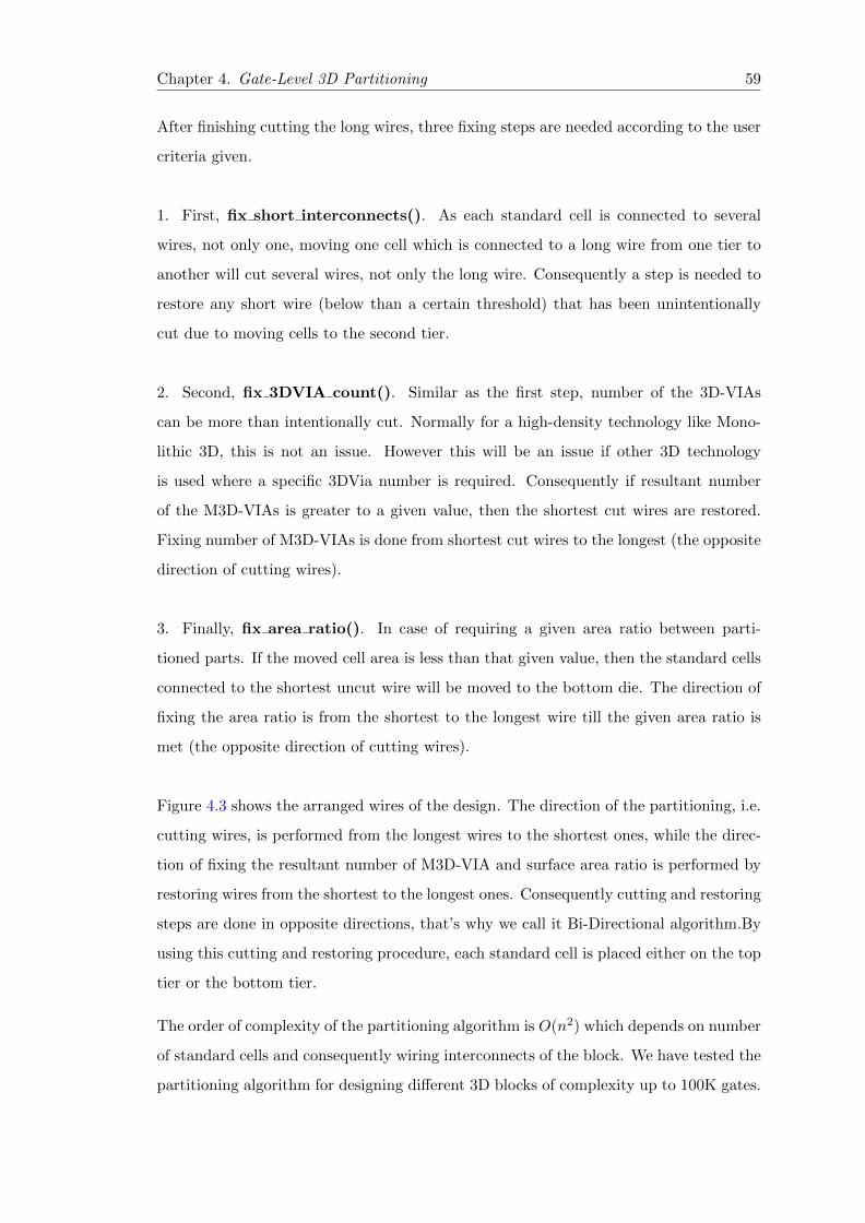
Chapter 4. Gate-Level 3D Partitioning 59
After finishing cutting the long wires, three fixing steps are needed according to the user
criteria given.
1. First, fix short interconnects(). As each standard cell is connected to several
wires, not only one, moving one cell which is connected to a long wire from one tier to
another will cut several wires, not only the long wire. Consequently a step is needed to
restore any short wire (below than a certain threshold) that has been unintentionally
cut due to moving cells to the second tier.
2. Second, fix 3DVIA count(). Similar as the first step, number of the 3D-VIAs
can be more than intentionally cut. Normally for a high-density technology like Mono-
lithic 3D, this is not an issue. However this will be an issue if other 3D technology
is used where a specific 3DVia number is required. Consequently if resultant number
of the M3D-VIAs is greater to a given value, then the shortest cut wires are restored.
Fixing number of M3D-VIAs is done from shortest cut wires to the longest (the opposite
direction of cutting wires).
3. Finally, fix area ratio(). In case of requiring a given area ratio between parti-
tioned parts. If the moved cell area is less than that given value, then the standard cells
connected to the shortest uncut wire will be moved to the bottom die. The direction of
fixing the area ratio is from the shortest to the longest wire till the given area ratio is
met (the opposite direction of cutting wires).
Figure 4.3 shows the arranged wires of the design. The direction of the partitioning, i.e.
cutting wires, is performed from the longest wires to the shortest ones, while the direc-
tion of fixing the resultant number of M3D-VIA and surface area ratio is performed by
restoring wires from the shortest to the longest ones. Consequently cutting and restoring
steps are done in opposite directions, that’s why we call it Bi-Directional algorithm.By
using this cutting and restoring procedure, each standard cell is placed either on the top
tier or the bottom tier.
The order of complexity of the partitioning algorithm is O(n2) which depends on number
of standard cells and consequently wiring interconnects of the block. We have tested the
partitioning algorithm for designing different 3D blocks of complexity up to 100K gates.
Chapter 4. Gate-Level 3D Partitioning 60
Figure 4.3: Bi-Directional Partitioning (BDP) diagram showing the design nets ar-ranged from the longes net to the shortest net where the cut wires is performed fromthe longest to the shortest one (down arrow) till a certain Cut Threshold, and restore
wires is performed from the shortest to the longest (up arrows).
4.5 Un-Balancing Area Ratio Concept
Balancing the area ratio between top and bottom tiers has been always used as it min-
imizes the 3D footprint area. This argument is true for the whole chip, however by
dealing with block-level (each block separately) the need for equal area between top and
bottom layers (balanced area ratio) is no longer a constraint. In this case a smart hybrid
3D floor-planning is needed for the whole chip (SoC) to place different blocks properly
and get the minimum footprint area by having equal top and bottom areas. Also having
equal top and bottom area is important to avoid impact on die packaging.
Figure 4.4 showing different blocks where each block has a different area ratio between
top and bottom layers, and even some blocks can be in 2D, while the whole chip have
balanced area to minimize the chip footprint area. Using such floor-planning avoids any
extra area in the whole chip packaging due to the unbalanced blocks. The concept of
having a 3D SoC with both 2D and balanced area ratio 3D blocks has been introduced in
[54]. Our proposal is to extend this concept so that the 3D SoC can include 2D blocks,
balanced 3D blocks and unbalanced 3D blocks.
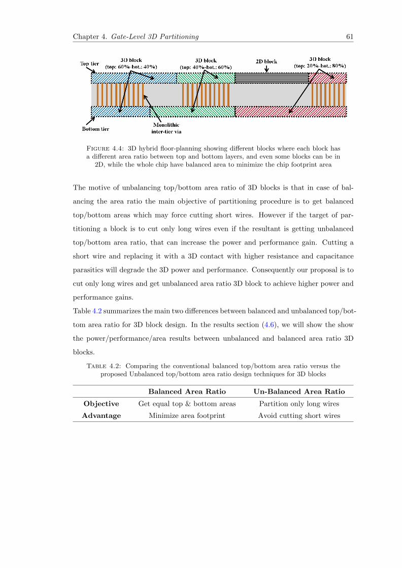
Chapter 4. Gate-Level 3D Partitioning 61
Figure 4.4: 3D hybrid floor-planning showing different blocks where each block hasa different area ratio between top and bottom layers, and even some blocks can be in
2D, while the whole chip have balanced area to minimize the chip footprint area
The motive of unbalancing top/bottom area ratio of 3D blocks is that in case of bal-
ancing the area ratio the main objective of partitioning procedure is to get balanced
top/bottom areas which may force cutting short wires. However if the target of par-
titioning a block is to cut only long wires even if the resultant is getting unbalanced
top/bottom area ratio, that can increase the power and performance gain. Cutting a
short wire and replacing it with a 3D contact with higher resistance and capacitance
parasitics will degrade the 3D power and performance. Consequently our proposal is to
cut only long wires and get unbalanced area ratio 3D block to achieve higher power and
performance gains.
Table 4.2 summarizes the main two differences between balanced and unbalanced top/bot-
tom area ratio for 3D block design. In the results section (4.6), we will show the show
the power/performance/area results between unbalanced and balanced area ratio 3D
blocks.
Table 4.2: Comparing the conventional balanced top/bottom area ratio versus theproposed Unbalanced top/bottom area ratio design techniques for 3D blocks
Balanced Area Ratio Un-Balanced Area Ratio
Objective Get equal top & bottom areas Partition only long wires
Advantage Minimize area footprint Avoid cutting short wires
Chapter 4. Gate-Level 3D Partitioning 62
4.6 Performance-Power-Area Results
4.6.1 PAP Methodology Implementation
To evaluate our approach, we have implemented a min-cut partitioning case with bal-
anced area ratio (50%-50%) using hMetis tool [25] and set it as our reference case. Our
proposed physical-aware partitioning (PAP) methodology has been implemented with
unbalancing the area ratio and relaxing the number of M3D vias. We have explored
as well the cases of balanced area ratio using PAP methodology, however to be focus,
we will discuss only unbalancing area ratio PAP case with the best performance gain.
A comparison is set between our performance-drive partitioning methodology and the
hMetis reference points. Our scope in this chapter is gate-level partitioning, so no com-
parison is performed with Architecture-level cases.
Our benchmark circuits are composed of growing complexity blocks: open-MSP micro-
controller, Reconfigurable Fast Fourier Transform (Reconf-FFT), Floating Point Unit
(FPU) and Low-Density Parity Check (LDPC) decoder.
To validate our different partitioning cases with timing and power results, we have de-
cided to prototype the physical implementation of our test-bench blocks using Atrenta
SpyGlass Physical 3D (SGP-3D) as a commercial 3D tool with FDSOI 28nm CMOS tech-
nology node and M3D technology parameters extracted from the work demonstrated in
[8].
The SGP-3D prototyping tool used is fully aware of physical implementation floor-
planning of both tiers, placement of both standard cells and M3D vias, global routing
and parasitic extraction. Figure 4.5 shows a snapshot for the physical implementation
of one of our benchmarks, the LDPC block, in hMetis balanced case (50%-50%) and
PAP unbalanced case (top: 75%, bottom: 25%). All the results presented are directly
outputted by the tool including routing report, Total Wire Length (TWL), time slack
(i.e. Performance) and Power.
In all test cases, we use M3D-VIA with a resistance of 2Ω and a capacitance of 0.1fF
[35]. For the 3D design partitioning, we have converted the resistance and capacitance
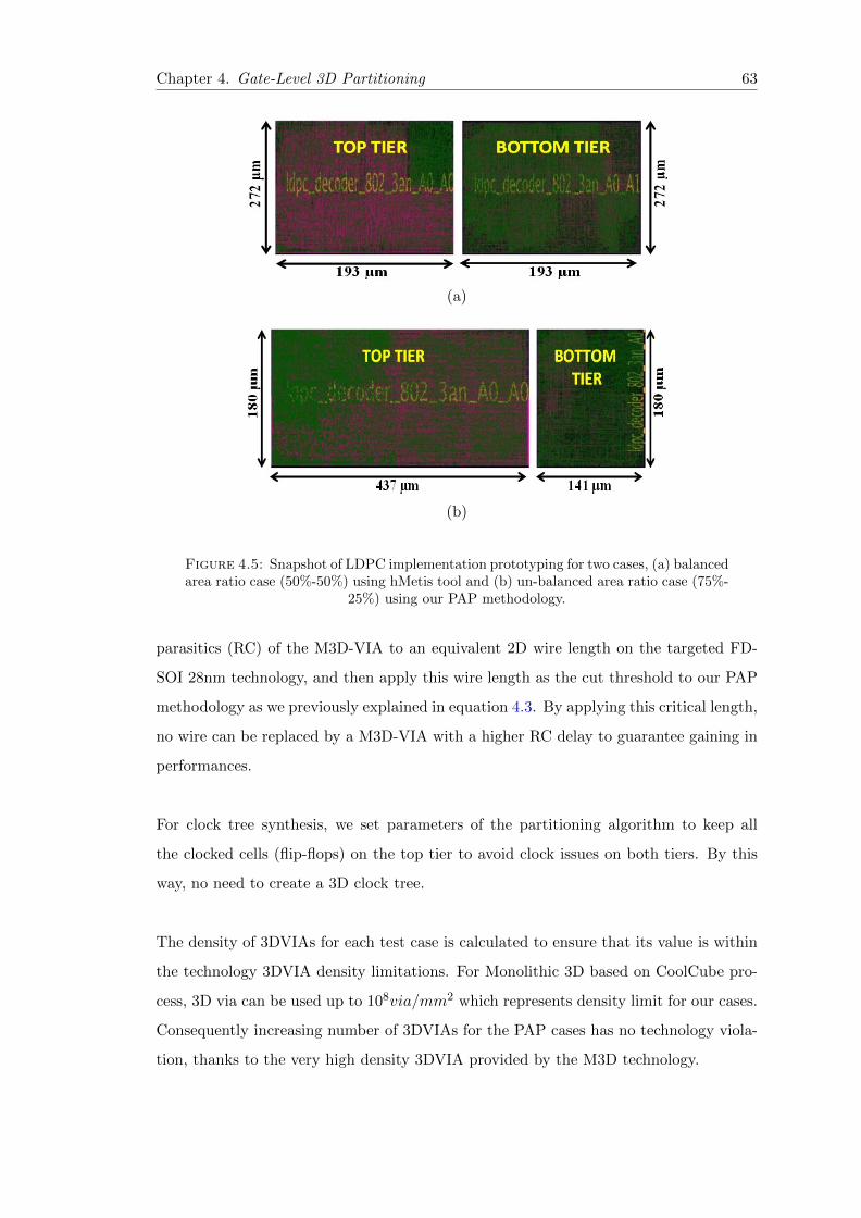
Chapter 4. Gate-Level 3D Partitioning 63
(a)
(b)
Figure 4.5: Snapshot of LDPC implementation prototyping for two cases, (a) balancedarea ratio case (50%-50%) using hMetis tool and (b) un-balanced area ratio case (75%-
25%) using our PAP methodology.
parasitics (RC) of the M3D-VIA to an equivalent 2D wire length on the targeted FD-
SOI 28nm technology, and then apply this wire length as the cut threshold to our PAP
methodology as we previously explained in equation 4.3. By applying this critical length,
no wire can be replaced by a M3D-VIA with a higher RC delay to guarantee gaining in
performances.
For clock tree synthesis, we set parameters of the partitioning algorithm to keep all
the clocked cells (flip-flops) on the top tier to avoid clock issues on both tiers. By this
way, no need to create a 3D clock tree.
The density of 3DVIAs for each test case is calculated to ensure that its value is within
the technology 3DVIA density limitations. For Monolithic 3D based on CoolCube pro-
cess, 3D via can be used up to 108via/mm2 which represents density limit for our cases.
Consequently increasing number of 3DVIAs for the PAP cases has no technology viola-
tion, thanks to the very high density 3DVIA provided by the M3D technology.
Chapter 4. Gate-Level 3D Partitioning 64
Table 4.3 summarizes the power, performance and area results for different benchmark
blocks. A comparison of three implementation cases is set: (i) 2D implementation, (ii)
3D with balanced area ratio using hMetis tool and (iii) 3D with unbalanced area ratio
using our PAP methodology.
4.6.2 Performance Results
PAP approach highlights that better performances can be obtained at unbalanced area
ratio. The unbalancing area ratio varies depending on the block design, i.e. the ratio
between number of long wires and short wires. In case of openMSP better performance
is obtained at (35-65) area ratio, while the area ratio is better at (40-60) for the Recon-
FFT, and (25-75) for the LDPC blocks. However PAP with balanced area ratio results
better performance than the balanced area ratio using hMetis.
The performance, shown in Table 4.3, is calculated by removing the positive time slack
to the frequency max of the clock used. The frequency max is the highest clock fre-
quency we target in the trial before getting high congestion effect.
For control-oriented block like openMSP, we can observe that increasing the number of
M3D-VIAS and un-balancing the area ratio by 31% can bring 17.4% better performance
than the 2D design but also 15% more performance than classical min-cut balanced
area ratio using hMetis. Similarly for the Reconfigurable-FFT block, unbalancing the
area ratio by 40% can achieve 24% better performance than 2D where hMetis increases
the performance only by 9%. It appears that the control-oriented blocks offer better
performance gains by unbalancing area ratio due to the presence of long control wiring
interconnects which is difficult to be optimized in 2D.
On the other hand, for the computing-oriented blocks like the LDPC, we show that
unbalancing area ratio with our PAP methodology can increase performances by 11.5%
compared to 2D which is slightly better than the hMetis.
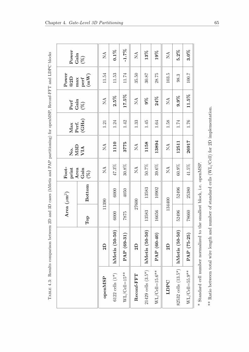
Chapter 4. Gate-Level 3D Partitioning 65
Table4.3:
Res
ult
sco
mp
aris
onb
etw
een
2Dan
d3D
case
s(h
Met
isan
dP
AP
part
itio
nin
g)
for
op
enM
SP
,R
econ
f-F
FT
an
dL
DP
Cb
lock
s
Are
a(µ
m2)
Foot-
pri
nt
Are
aG
ain
(%)
No.
M3D
VIA
Max
Perf
.(G
Hz)
Perf
Gain
(%)
Pow
er
@2D
max
perf
(mW
)
Pow
er
Gain
(%)
Top
Bott
om
op
en
MS
P2D
1139
0N
AN
A1.
21N
A11
.54
NA
6122
cell
s(1
*)
hM
eti
s(5
0-5
0)
6000
6000
47.3
%1110
1.24
2.5
%11
.53
0.1
%
WL
/C
ell=
15*
*P
AP
(69-3
1)
7875
4050
30.8
%3775
1.42
17.5
%11
.74
-1.7
%
Recon
f-F
FT
2D
2760
0N
AN
A1.
33N
A35
.50
NA
214
29ce
lls
(3.5
*)
hM
eti
s(5
0-5
0)
1358
313
583
50.7
%1158
1.45
9%
30.8
713%
WL
/C
ell=
15.
6**
PA
P(6
0-4
0)
1665
610
902
39.6
%13894
1.64
24%
28.7
519%
LD
PC
2D
1344
00N
AN
A1.
58N
A10
3.5
NA
825
32ce
lls
(13.5
*)h
Meti
s(5
0-5
0)
5249
652
496
60.9
%12511
1.74
9.9
%98
.35.2
%
WL
/C
ell=
55.
9**
PA
P(7
5-2
5)
7866
025
380
41.5
%26917
1.76
11.5
%10
0.7
3.0
%
*S
tan
dar
dce
llnu
mb
ern
orm
ali
zed
toth
esm
alle
stb
lock
,i.
e.op
enM
SP
.
**
Rat
iob
etw
een
tota
lw
ire
len
gth
and
nu
mb
erof
stan
dar
dce
lls
(WL
/Cel
l)fo
r2D
imp
lem
enta
tion
.
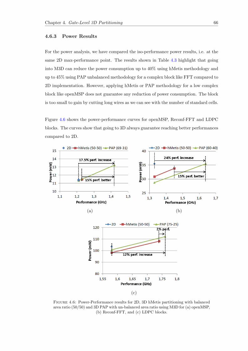
Chapter 4. Gate-Level 3D Partitioning 66
4.6.3 Power Results
For the power analysis, we have compared the iso-performance power results, i.e. at the
same 2D max-performance point. The results shown in Table 4.3 highlight that going
into M3D can reduce the power consumption up to 40% using hMetis methodology and
up to 45% using PAP unbalanced methodology for a complex block like FFT compared to
2D implementation. However, applying hMetis or PAP methodology for a low complex
block like openMSP does not guarantee any reduction of power consumption. The block
is too small to gain by cutting long wires as we can see with the number of standard cells.
Figure 4.6 shows the power-performance curves for openMSP, Reconf-FFT and LDPC
blocks. The curves show that going to 3D always guarantee reaching better performances
compared to 2D.
(a) (b)
(c)
Figure 4.6: Power-Performance results for 2D, 3D hMetis partitioning with balancedarea ratio (50/50) and 3D PAP with un-balanced area ratio using M3D for (a) openMSP,
(b) Reconf-FFT, and (c) LDPC blocks.
Chapter 4. Gate-Level 3D Partitioning 67
4.7 Summary and Conclusion
In this chapter we have demonstrated that partitioning the design with M3D integra-
tion technology involves a trade-off between number of M3D-VIAS, area ratio, power
consumption and overall performance of the 3D design.
Minimizing number of M3D-VIA and targeting balanced area ratio are no longer ef-
ficient as the main constraints to partition designs for high density 3D technologies. We
have setup a physical-aware partitioning (PAP) methodology based on a Bi-Directional
Partitioning (BDP) algorithm to decide which wire has to be cut and which cell is as-
signed to which tier.
Additionally We have proposed an unbalanced area ratio technique integrated in the
physical-aware partitioning methodology. Unbalanced area ratio concept tends improve
the performance gain by partitioning only long wires of the design without taking into
account achieving area balance as a constraint. A hybrid floor-planning for different
blocks is shown to avoid any extra space in the whole chip area.
We have applied PAP methodology on a set of different growing complexity bench-
marks. The physical implementation results show that we can gain in performance up
to 24% compared to 2D design and up to 15% more compared to area balanced and
min-cut 3D design. On the other hand for iso-performance cases, we show that 3D
blocks with unbalanced area ratio reduce power consumption up to 22% compared to
2D and up to 12% more compared to area balanced and min-cut 3D designs.
Chapter 5
Intermediate BEOL process
influence for M3D
5.1 Introduction: Effect of Intermediate-BEOL for M3D
Monolithic 3D (3DVLSI) technology based on CoolCubeTM process offers ultra-high
density of integration with up to 108 3D Vias (3D-V) per mm2 offering gate level 3D
integration capability [8]. As CoolCubeTM process is an advanced technology, there is a
need to perform technology assessment to give guidelines at design level to the process
and technology teams.
One of the important questions is the effect of Intermediate Back-End-Of-Line (I-BEOL).
I-BEOL is the metal layer stack of the bottom tier, so it is an intermediate layer between
top and bottom tiers.For process stability and wide range of temperature compliance,
Intermediate Back End of Line (I-BEOL) is targeted to be made with Tungsten (W)
lines with a SiO2 dielectric (k=3.9), which increase the equivalent resistivity by 6 and
capacitance by 1.6 compared to standard Back End of Line (BEOL), i.e. Copper (Cu)
lines in low-k dielectrics.
In this chapter a study is performed to show the impact in Power and Performance
by using W/SiO2 compared to Cu/low-k I-BEOL.
68
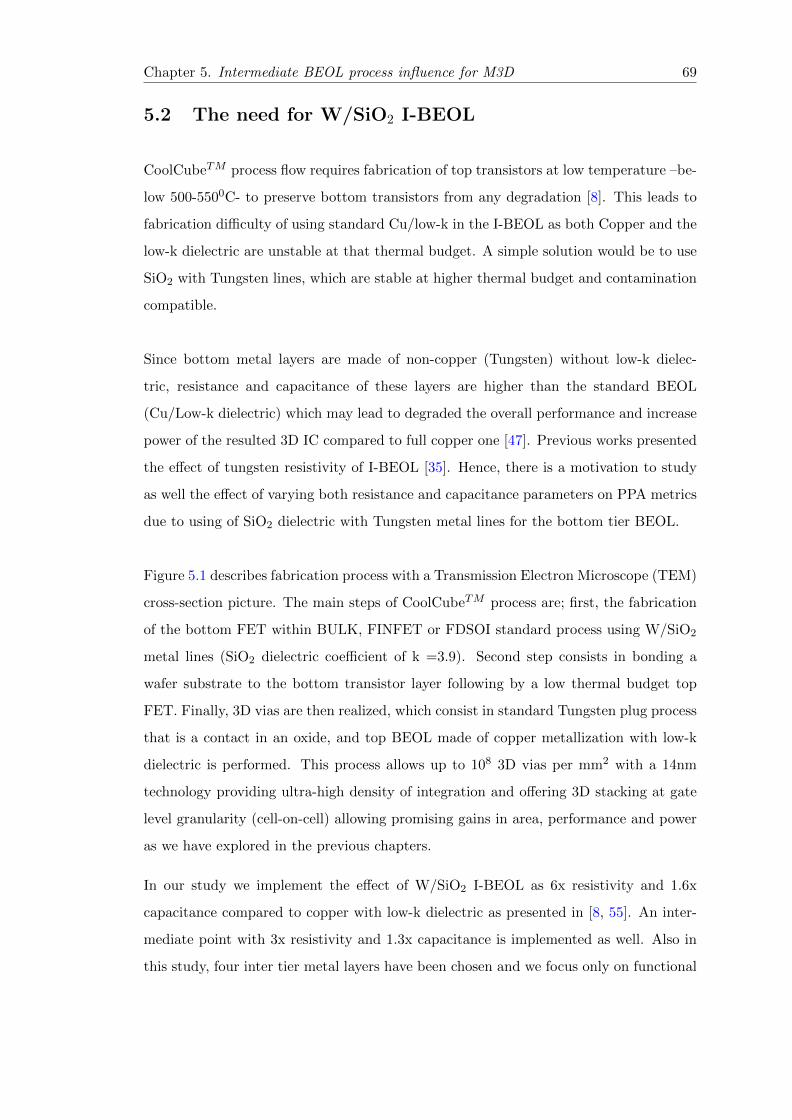
Chapter 5. Intermediate BEOL process influence for M3D 69
5.2 The need for W/SiO2 I-BEOL
CoolCubeTM process flow requires fabrication of top transistors at low temperature –be-
low 500-5500C- to preserve bottom transistors from any degradation [8]. This leads to
fabrication difficulty of using standard Cu/low-k in the I-BEOL as both Copper and the
low-k dielectric are unstable at that thermal budget. A simple solution would be to use
SiO2 with Tungsten lines, which are stable at higher thermal budget and contamination
compatible.
Since bottom metal layers are made of non-copper (Tungsten) without low-k dielec-
tric, resistance and capacitance of these layers are higher than the standard BEOL
(Cu/Low-k dielectric) which may lead to degraded the overall performance and increase
power of the resulted 3D IC compared to full copper one [47]. Previous works presented
the effect of tungsten resistivity of I-BEOL [35]. Hence, there is a motivation to study
as well the effect of varying both resistance and capacitance parameters on PPA metrics
due to using of SiO2 dielectric with Tungsten metal lines for the bottom tier BEOL.
Figure 5.1 describes fabrication process with a Transmission Electron Microscope (TEM)
cross-section picture. The main steps of CoolCubeTM process are; first, the fabrication
of the bottom FET within BULK, FINFET or FDSOI standard process using W/SiO2
metal lines (SiO2 dielectric coefficient of k =3.9). Second step consists in bonding a
wafer substrate to the bottom transistor layer following by a low thermal budget top
FET. Finally, 3D vias are then realized, which consist in standard Tungsten plug process
that is a contact in an oxide, and top BEOL made of copper metallization with low-k
dielectric is performed. This process allows up to 108 3D vias per mm2 with a 14nm
technology providing ultra-high density of integration and offering 3D stacking at gate
level granularity (cell-on-cell) allowing promising gains in area, performance and power
as we have explored in the previous chapters.
In our study we implement the effect of W/SiO2 I-BEOL as 6x resistivity and 1.6x
capacitance compared to copper with low-k dielectric as presented in [8, 55]. An inter-
mediate point with 3x resistivity and 1.3x capacitance is implemented as well. Also in
this study, four inter tier metal layers have been chosen and we focus only on functional
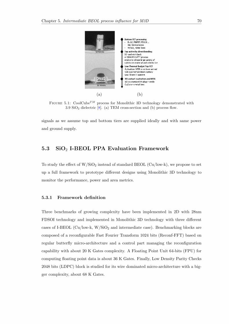
Chapter 5. Intermediate BEOL process influence for M3D 70
(a) (b)
Figure 5.1: CoolCubeTM process for Monolithic 3D technology demonstrated with3.9 SiO2 dielectric [8]. (a) TEM cross-section and (b) process flow.
signals as we assume top and bottom tiers are supplied ideally and with same power
and ground supply.
5.3 SiO2 I-BEOL PPA Evaluation Framework
To study the effect of W/SiO2 instead of standard BEOL (Cu/low-k), we propose to set
up a full framework to prototype different designs using Monolithic 3D technology to
monitor the performance, power and area metrics.
5.3.1 Framework definition
Three benchmarks of growing complexity have been implemented in 2D with 28nm
FDSOI technology and implemented in Monolithic 3D technology with three different
cases of I-BEOL (Cu/low-k, W/SiO2 and intermediate case). Benchmarking blocks are
composed of a reconfigurable Fast Fourier Transform 1024 bits (Reconf-FFT) based on
regular butterfly micro-architecture and a control part managing the reconfiguration
capability with about 20 K Gates complexity. A Floating Point Unit 64-bits (FPU) for
computing floating point data is about 36 K Gates. Finally, Low Density Parity Checks
2048 bits (LDPC) block is studied for its wire dominated micro-architecture with a big-
ger complexity, about 68 K Gates.
Chapter 5. Intermediate BEOL process influence for M3D 71
Benchmarks are first synthesized with 28-nm FDSOI technology to obtain a 2D logi-
cal netlist of each block. Partitioning 2D netlist into two 3D netlists is then performed
in order to get top and bottom netlists which is expected by the implementation pro-
totyping tool. HMetis tool [25] has been used to partition 2D netlist and consequently
generate 3D netlists with equal cell area between top and bottom layers. Partitioning
step is performed after synthesis which presents an advantage of using 2D block gate-
netlist without updating the micro-architecture and the RTL code which is important
from time-to-market perspective.
Afterwards, physical implementation prototyping is performed with Atrenta SpyGlass
Physical (SGP) tool [48] as a commercial tool to get early performance, power and area
results for 2D and M3D implementations. As Monolithic 3D technology offers ultra-
high density of integration with the capability of stacking cells over cells, this feature
is not supported well in common place and route tool. That is why we have chosen to
prototype physical implementation to bypass limitations in place and route tool, tak-
ing advantage of the capability of the tool to perform 3D floor-planning, clustering and
macro placement of cells, creating 3D vias based on 3D stack configuration XML file
and finally applying global routing. After each step the tool provides optimization ca-
pabilities leading to put 3D via on an optimal coarse grain position and place standard
cells around, offering global 3D placement optimization.
The SGP tool can extract parasitics at the end of the flow in line with resistivity and
capacitance of metallization lines contained in technology files and thus it can perform
timing analysis and power estimation based on 28 nm FDSOI gates timing libraries (.lib)
with top and bottom BEOL parasitics extraction.
Physical implementation prototyping is done in 2D with copper BEOL extraction then
in 3D as illustrated in Figure 5.2 still with copper BEOL and I-BEOL. W/SiO2 effect
is applied by updating SPEF extraction file with resistivity and capacitance values de-
fined for intermediate and W/SiO2 cases. The next section explains overall focuses on
updating the parasitics file with tungsten and SiO2 dielectric values.
Chapter 5. Intermediate BEOL process influence for M3D 72
Figure 5.2: PPA implementation prototype methodology to compare different bottommetal layers effect.
5.3.2 I-BEOL parasitics extraction focus
In this section we focus on updating the parasitics to reflect the effect of I-BEOL with
different flavours. After 3D placement and routing, the tool generates a SPEF file which
is composed of top and bottom Cu/low-k BEOL parasitics without 3D vias contributions.
Two different steps are needed to be done here: (i) take into account the 3D via resistance
and capacitance contributions and (ii) update I-BEOL parasitics with intermediate and
W/SiO2 parasitics instead of the copper/low-k.
Procedure 2 shows the algorithm used to update SPEF file with 3D via parastics and
different I-BEOL parasitics. First step is to add the 3D via resistance (Res 3Dvia) and
capacitance (Cap 3Dvia) as introduced previously. For this, a script parses the SPEF file
to find all 3D connections going from one tier to another, and add values for Res 3Dvia
and Cap 3Dvia. Once the SPEF file is updated, it re-inserted in the tool so that timing
analysis and power estimation are performed back in the tool to obtain results including
the effect of 3D via.
The second step is to update the SPEF file with the contribution of intermediate BEOL.
The original BEOL used is Copper with low-k dielectric. Tungsten BEOL with SiO2
dielectric has 6x resistance and 1.6x capacitance compared to Cu/low-k. An intermediate
case has been selected with 3x resistivity and 1.3x capacitance compared to Cu/low-k
BEOL. To achieve that, a script parses the SPEF file to find the bottom connections
and multiply resistance and capacitance to include the effect of I-BEOL. Similar to the
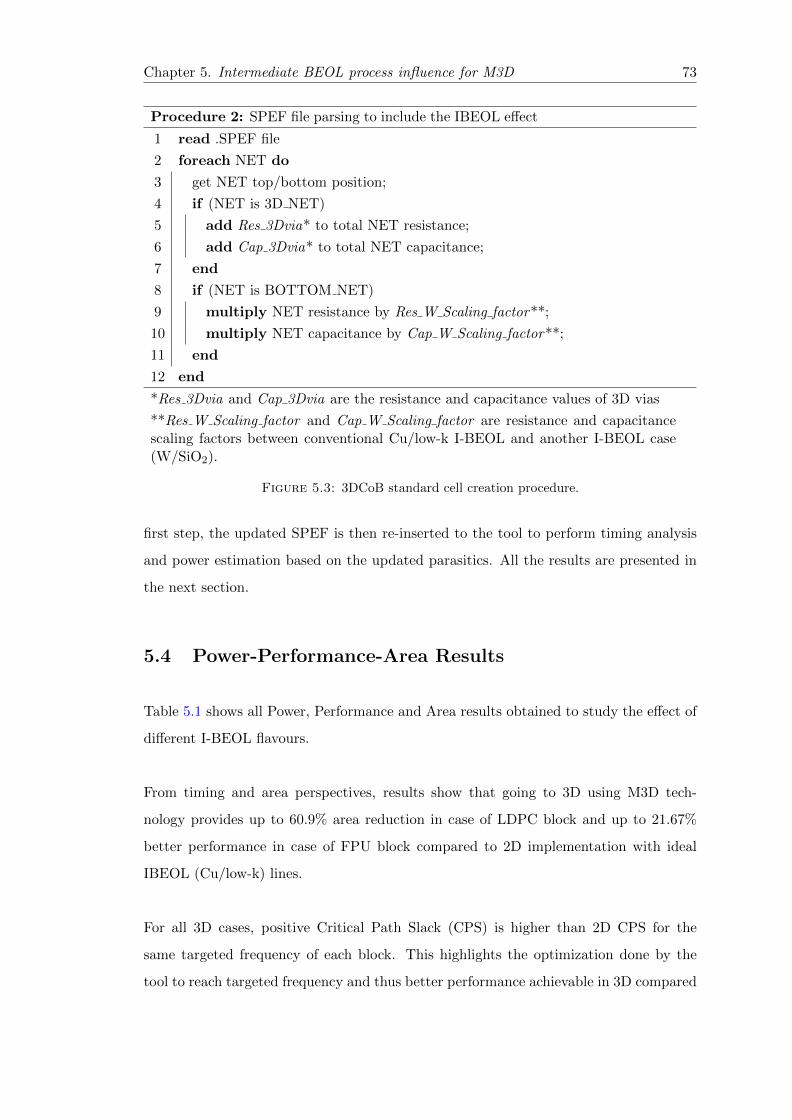
Chapter 5. Intermediate BEOL process influence for M3D 73
Procedure 2: SPEF file parsing to include the IBEOL effect
1 read .SPEF file
2 foreach NET do
3 get NET top/bottom position;
4 if (NET is 3D NET)
5 add Res 3Dvia* to total NET resistance;
6 add Cap 3Dvia* to total NET capacitance;
7 end
8 if (NET is BOTTOM NET)
9 multiply NET resistance by Res W Scaling factor**;
10 multiply NET capacitance by Cap W Scaling factor**;
11 end
12 end
*Res 3Dvia and Cap 3Dvia are the resistance and capacitance values of 3D vias
**Res W Scaling factor and Cap W Scaling factor are resistance and capacitancescaling factors between conventional Cu/low-k I-BEOL and another I-BEOL case(W/SiO2).
Figure 5.3: 3DCoB standard cell creation procedure.
first step, the updated SPEF is then re-inserted to the tool to perform timing analysis
and power estimation based on the updated parasitics. All the results are presented in
the next section.
5.4 Power-Performance-Area Results
Table 5.1 shows all Power, Performance and Area results obtained to study the effect of
different I-BEOL flavours.
From timing and area perspectives, results show that going to 3D using M3D tech-
nology provides up to 60.9% area reduction in case of LDPC block and up to 21.67%
better performance in case of FPU block compared to 2D implementation with ideal
IBEOL (Cu/low-k) lines.
For all 3D cases, positive Critical Path Slack (CPS) is higher than 2D CPS for the
same targeted frequency of each block. This highlights the optimization done by the
tool to reach targeted frequency and thus better performance achievable in 3D compared
Chapter 5. Intermediate BEOL process influence for M3D 74
to 2D. The full analysis and results for 2D versus 3D (Cu/low-k BEOL case) have been
presented in the previous chapter(4).
Afterwards, we compare different I-BEOL flavors impact within intermediate case and
W/SiO2 by updating the SPEF parasitics file as explained earlier. The ratio between
the Total Wire Length and number of cells (WL/Cell) is used to represent the wire dom-
inance of each block. For blocks that are not wire dominated, we expect insignificant
impact on performance for both intermediate and W/SiO2 cases. Reconf-FFT and FPU
that present WL/Cell ratio respectively of 15.6 and 16.2 show performance degradation
less than 1% for W/SiO2 IBEOL compared to Cu/low-k case.
But for LDPC block, the performance degraded down to around 2% by using tung-
sten I-BEOL (W/SiO2) compared to the Cu/low-k case. The WL/Cell ratio of the
LDPC block equal to 55.9 and it shows 1.8x higher number of cells compared to FPU,
means that total wire length is 6.28 wider due to larger number of cells. Consequently
tungsten I-BEOL starts to show effect on wire dominated blocks but still within very
limited percentage for performance.
Power estimation is performed for 3D blocks to monitor the effect of using W/SiO2
I-BEOL. Similar to the performance trend, the non-wire-dominant blocks shows in-
significant power degradation, i.e. less than 1% for FFT and FPU blocks. For the
LDPC block, only 1.4% power increase is shown by using Tungsten with SiO2 I-BEOL
compared to the Copper with low-k dielectric.
Another important result is number of 3D vias used for each block and their impact
in term of area overhead. For instance 12511 3D vias are used for the LDPC block,
which is the biggest block, leading to a density of 2.38x10⁵ per mm2 with only area
overhead of 0.29% compared to the block footprint area. This number of 3D vias is
used for functional signals, however additional 3D vias is needed for power distribution
network (PDN) which can be up to 103 3D vias per mm2. Limited area overhead and
large number of 3D vias is due to the very small pitch of Monolithic 3D technology using
CoolCube process.
Figure 5.4 shows the power-performance results for FFT, FPU and LDPC blocks using
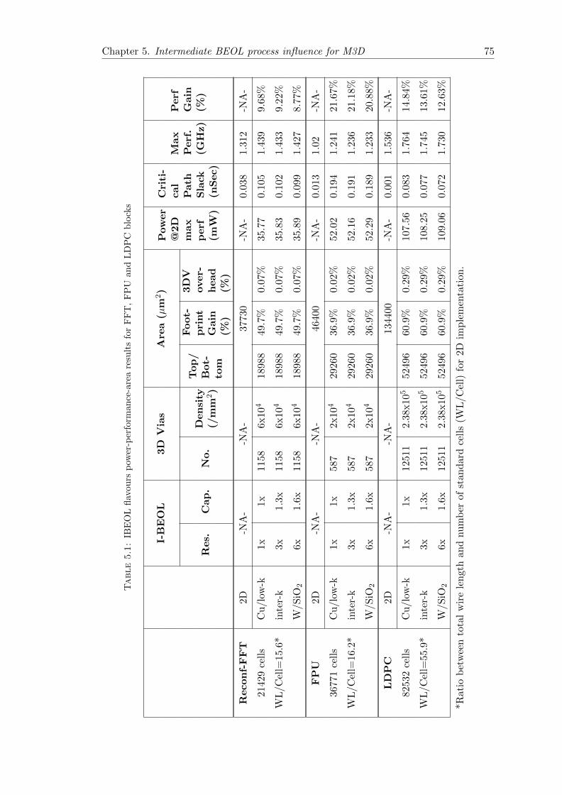
Chapter 5. Intermediate BEOL process influence for M3D 75
Table5.1:
IBE
OL
flav
ours
pow
er-p
erfo
rman
ce-a
rea
resu
lts
for
FF
T,
FP
Uan
dL
DP
Cb
lock
s
I-B
EO
L3D
Via
sA
rea
(µm
2)
Pow
er
@2D
max
perf
(mW
)
Cri
ti-
cal
Path
Sla
ck(n
Sec)
Max
Perf
.(G
Hz)
Perf
Gain
(%)
Res.
Cap
.N
o.
Den
sity
(/m
m2)
Top
/B
ot-
tom
Foot-
pri
nt
Gain
(%)
3D
Vover-
head
(%)
Recon
f-F
FT
2D-N
A-
-NA
-37
730
-NA
-0.
038
1.31
2-N
A-
2142
9ce
lls
Cu
/lo
w-k
1x1x
1158
6x10
418
988
49.7
%0.
07%
35.7
70.
105
1.43
99.
68%
WL
/Cel
l=15
.6*
inte
r-k
3x1.
3x11
586x
104
1898
849
.7%
0.07
%35
.83
0.10
21.
433
9.22
%
W/S
iO2
6x1.
6x11
586x
104
1898
849
.7%
0.07
%35
.89
0.09
91.
427
8.77
%
FP
U2D
-NA
--N
A-
4640
0-N
A-
0.01
31.
02-N
A-
3677
1ce
lls
Cu
/lo
w-k
1x1x
587
2x10
429
260
36.9
%0.
02%
52.0
20.
194
1.24
121
.67%
WL
/Cel
l=16
.2*
inte
r-k
3x1.
3x58
72x
104
2926
036
.9%
0.02
%52
.16
0.19
11.
236
21.1
8%
W/S
iO2
6x1.
6x58
72x
104
2926
036
.9%
0.02
%52
.29
0.18
91.
233
20.8
8%
LD
PC
2D-N
A-
-NA
-13
4400
-NA
-0.
001
1.53
6-N
A-
8253
2ce
lls
Cu
/lo
w-k
1x1x
1251
12.
38x10
552
496
60.9
%0.
29%
107.
560.
083
1.76
414
.84%
WL
/Cel
l=55
.9*
inte
r-k
3x1.
3x12
511
2.38
x10
552
496
60.9
%0.
29%
108.
250.
077
1.74
513
.61%
W/S
iO2
6x1.
6x12
511
2.38
x10
552
496
60.9
%0.
29%
109.
060.
072
1.73
012
.63%
*R
ati
ob
etw
een
tota
lw
ire
len
gth
an
dnu
mb
erof
stan
dar
dce
lls
(WL
/Cel
l)fo
r2D
imp
lem
enta
tion
.
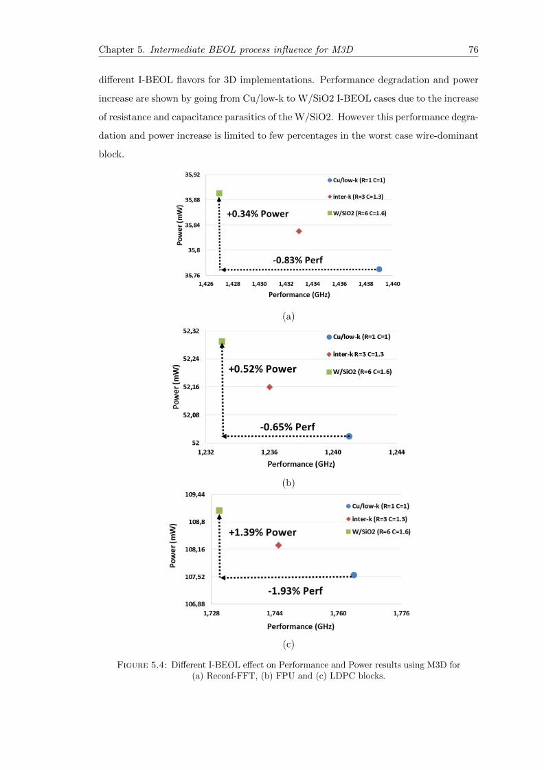
Chapter 5. Intermediate BEOL process influence for M3D 76
different I-BEOL flavors for 3D implementations. Performance degradation and power
increase are shown by going from Cu/low-k to W/SiO2 I-BEOL cases due to the increase
of resistance and capacitance parasitics of the W/SiO2. However this performance degra-
dation and power increase is limited to few percentages in the worst case wire-dominant
block.
(a)
(b)
(c)
Figure 5.4: Different I-BEOL effect on Performance and Power results using M3D for(a) Reconf-FFT, (b) FPU and (c) LDPC blocks.
Chapter 5. Intermediate BEOL process influence for M3D 77
5.5 Summary and Conclusion
In this chapter we have presented a framework to evaluate the effect of non-copper I-
BEOL (Tungsten with SiO2 dielectric) needed for CoolCubeTM process. The power and
performance results show limited effect of such W/SiO2 I-BEOL compared to conven-
tional Cu/low-k I-BEOL, i.e. below 2% performance degradation and below 1.5% power
increase. These results are function of block complexity, partitioning used, implementa-
tion framework and the CMOS technology node used.
Due to the presence of different high-density 3D technologies, a full framework is still
needed to perform technology assessment for these different 3D technologies. Such tech-
nology assessment is important to give us a guideline to use which technology with which
block complexity using which partitioning technique. Consequently, a 3D technology as-
sessment is presented in the next chapter.
Chapter 6
3D Technologies Assessment
“There is no one-size-fits-all”, so, Which 3D technology fits your design?
6.1 Introduction
The variety of 3D technology spectrum requires an exploration framework to determine
which technology fits which design. In the previous section, a design evaluation is per-
formed to show the effect of the I-BEOL process for Monolithic 3D. In this section, a
comprehensive assessment is performed to explore which high density 3D technology
among High-Density Through-Silicon-Via (HD-TSV), Copper-to-Copper contact (Cu-
Cu) and Monolithic 3D (M3D) provides best Performance, Power and Area (PPA).
We introduce a design frame work to determine quickly and efficiently which 3D tech-
nology brings up best PPA considering partitioning algorithm, complexity and type of
block (wire oriented, computation ...) for CMOS 28nm technology at 3D IC exploration
and architecture definition.
HD-TSV and Cu-Cu technologies are based on post-fabrication assembly process of
both tiers. Silicon demonstrators of full chips have already fabricated using these tech-
nologies in [10, 20, 26] which show major gains compared to 2D. Monolithic 3D is an
78
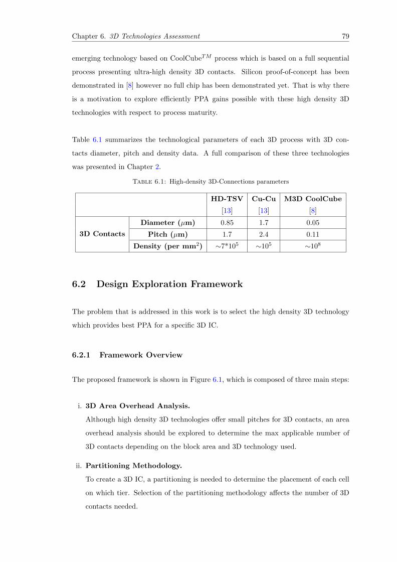
Chapter 6. 3D Technologies Assessment 79
emerging technology based on CoolCubeTM process which is based on a full sequential
process presenting ultra-high density 3D contacts. Silicon proof-of-concept has been
demonstrated in [8] however no full chip has been demonstrated yet. That is why there
is a motivation to explore efficiently PPA gains possible with these high density 3D
technologies with respect to process maturity.
Table 6.1 summarizes the technological parameters of each 3D process with 3D con-
tacts diameter, pitch and density data. A full comparison of these three technologies
was presented in Chapter 2.
Table 6.1: High-density 3D-Connections parameters
HD-TSV Cu-Cu M3D CoolCube
[13] [13] [8]
3D Contacts
Diameter (µm) 0.85 1.7 0.05
Pitch (µm) 1.7 2.4 0.11
Density (per mm2) ∼7*105 ∼105 ∼108
6.2 Design Exploration Framework
The problem that is addressed in this work is to select the high density 3D technology
which provides best PPA for a specific 3D IC.
6.2.1 Framework Overview
The proposed framework is shown in Figure 6.1, which is composed of three main steps:
i. 3D Area Overhead Analysis.
Although high density 3D technologies offer small pitches for 3D contacts, an area
overhead analysis should be explored to determine the max applicable number of
3D contacts depending on the block area and 3D technology used.
ii. Partitioning Methodology.
To create a 3D IC, a partitioning is needed to determine the placement of each cell
on which tier. Selection of the partitioning methodology affects the number of 3D
contacts needed.
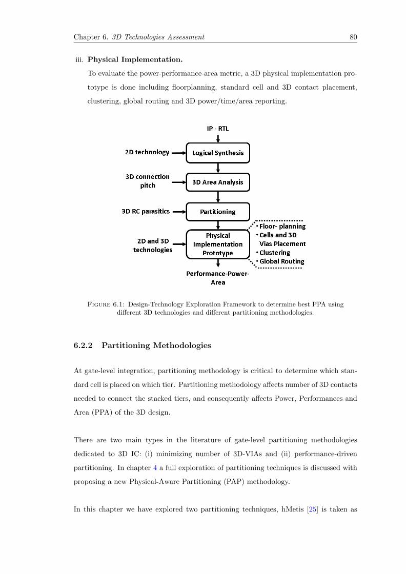
Chapter 6. 3D Technologies Assessment 80
iii. Physical Implementation.
To evaluate the power-performance-area metric, a 3D physical implementation pro-
totype is done including floorplanning, standard cell and 3D contact placement,
clustering, global routing and 3D power/time/area reporting.
Figure 6.1: Design-Technology Exploration Framework to determine best PPA usingdifferent 3D technologies and different partitioning methodologies.
6.2.2 Partitioning Methodologies
At gate-level integration, partitioning methodology is critical to determine which stan-
dard cell is placed on which tier. Partitioning methodology affects number of 3D contacts
needed to connect the stacked tiers, and consequently affects Power, Performances and
Area (PPA) of the 3D design.
There are two main types in the literature of gate-level partitioning methodologies
dedicated to 3D IC: (i) minimizing number of 3D-VIAs and (ii) performance-driven
partitioning. In chapter 4 a full exploration of partitioning techniques is discussed with
proposing a new Physical-Aware Partitioning (PAP) methodology.
In this chapter we have explored two partitioning techniques, hMetis [25] is taken as
Chapter 6. 3D Technologies Assessment 81
an example of min-cut partitioning and our PAP methodology is taken as an example
of performance-driven partitioning.
HMetis tool is a min-cut partitioning which optimizes number of interconnects between
two partitions. In reference [26], hMetis has been used as a min-cut partitioning algo-
rithm to achieve 50-50 area ratio for DSP block based on Cu-Cu technology of 5µm 3D
contact pitch.
On the other hand, PAP methodology breaks the idea of min-cut partitioning by using
a multi-criteria optimization algorithm; i.e. area ratio between stacked tiers, critical
length threshold, and number of 3D contacts. By applying performance-driven parti-
tioning, number of 3D-VIAs can exceed that of the min-cut partitioning algorithm to
achieve better power-performance results.
6.3 3D Area Overhead analysis
Area and density of 3D contacts affects the decision of using the proper partitioning
methodology; either targets minimizing number of 3D contacts or increasing perfor-
mance with no constraints on 3D contacts count.
To show the area cost of 3D count, an early exploration study is introduced using
growing complexity blocks based on different high density 3D technologies.
6.3.1 3D Contact Area Overhead Model
3D contact area penalty is the extra area needed by vertical connections exceeding the
ideal 3D area footprint, ‘Area 3D ideal’. The ideal 3D area is defined as the area oc-
cupied by standard cells and routing without taking into consideration the area of 3D
contacts. It can be estimated by dividing the 2D area by number of stacked layers, i.e. 2.
Consequently 3D contact area overhead penalty can be calculated as shown in equa-
tion 6.1.
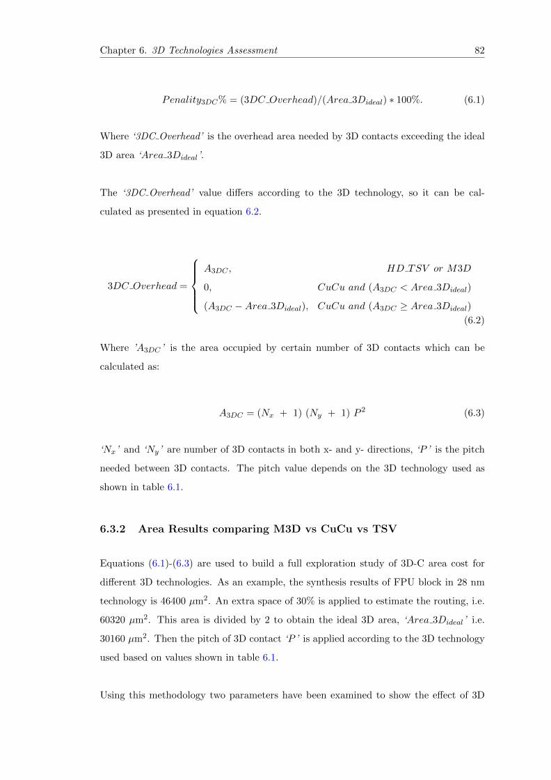
Chapter 6. 3D Technologies Assessment 82
Penality3DC% = (3DC Overhead)/(Area 3Dideal) ∗ 100%. (6.1)
Where ‘3DC Overhead’ is the overhead area needed by 3D contacts exceeding the ideal
3D area ‘Area 3Dideal’.
The ‘3DC Overhead’ value differs according to the 3D technology, so it can be cal-
culated as presented in equation 6.2.
3DC Overhead =
A3DC , HD TSV or M3D
0, CuCu and (A3DC < Area 3Dideal)
(A3DC −Area 3Dideal), CuCu and (A3DC ≥ Area 3Dideal)
(6.2)
Where ’A3DC ’ is the area occupied by certain number of 3D contacts which can be
calculated as:
A3DC = (Nx + 1) (Ny + 1) P 2 (6.3)
‘Nx’ and ‘Ny’ are number of 3D contacts in both x- and y- directions, ‘P ’ is the pitch
needed between 3D contacts. The pitch value depends on the 3D technology used as
shown in table 6.1.
6.3.2 Area Results comparing M3D vs CuCu vs TSV
Equations (6.1)-(6.3) are used to build a full exploration study of 3D-C area cost for
different 3D technologies. As an example, the synthesis results of FPU block in 28 nm
technology is 46400 µm2. An extra space of 30% is applied to estimate the routing, i.e.
60320 µm2. This area is divided by 2 to obtain the ideal 3D area, ‘Area 3Dideal’ i.e.
30160 µm2. Then the pitch of 3D contact ‘P ’ is applied according to the 3D technology
used based on values shown in table 6.1.
Using this methodology two parameters have been examined to show the effect of 3D
Chapter 6. 3D Technologies Assessment 83
contacts area overhead;
(i) increasing number of 3D contacts for a specific block, and
(ii) increasing block complexity at certain number of 3D contact.
Table 6.2 shows the Area overhead effect of increasing density of 3D contacts per gate
count. Number of 3D contact is calculated for a 15K gates block as an example. As ex-
pected, 3D contacts area overhead penalty increases as number of 3D contact increases.
The 100% area overhead means that the total block area, i.e. both gates and 3D contact
areas, will reach the original 2D area.
Consequently exceeding the 100% limit, removes any area gain by 3D design. We can
notice that HD-TSV and Cu-Cu exceed the original 2D area at 26% 3D-C density (i.e.
4000 3D contacts for 15K gate block). However Monolithic 3D overhead is almost within
1% from the ideal 3D area.
Figure 6.2 shows the effect of growing block complexity at certain 3D contacts count. As
number of block gates increases, the block area increases which decrease the area over-
head of 3D contacts. For HD-TSV case, 3D contacts area penalty reduced from 164%
to 68.4% by doubling block complexity from 15K to 30K gates at 5000 3D contacts.
In all cases, M3D provides insignificant area penalty but for big circuits and 28nm
FDSOI technology CuCu has limited area overhead. HD-TSV can be an alternative
only for big circuits (more than hundred thousands of gates).
6.3.3 Discussion: Partitioning Effect for 3D-C Area
From the aforementioned results we can notice that using HD-TSV and Cu-Cu tech-
nologies for small blocks, number of 3D contacts creates an area overhead penalty and
affects the total area of the 3D block. Consequently using min-cut partitioning algo-
rithm is mandatory to minimize number of 3D contacts needed. For larger blocks that
area penalty decreases but still 3D block can exceeds the area of the 2D block for large
number of 3D contacts.
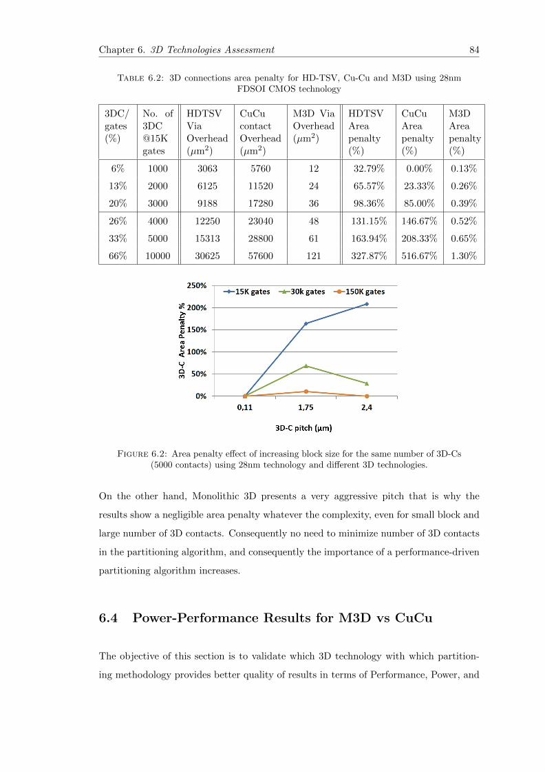
Chapter 6. 3D Technologies Assessment 84
Table 6.2: 3D connections area penalty for HD-TSV, Cu-Cu and M3D using 28nmFDSOI CMOS technology
3DC/gates(%)
No. of3DC@15Kgates
HDTSVViaOverhead(µm2)
CuCucontactOverhead(µm2)
M3D ViaOverhead(µm2)
HDTSVAreapenalty(%)
CuCuAreapenalty(%)
M3DAreapenalty(%)
6% 1000 3063 5760 12 32.79% 0.00% 0.13%
13% 2000 6125 11520 24 65.57% 23.33% 0.26%
20% 3000 9188 17280 36 98.36% 85.00% 0.39%
26% 4000 12250 23040 48 131.15% 146.67% 0.52%
33% 5000 15313 28800 61 163.94% 208.33% 0.65%
66% 10000 30625 57600 121 327.87% 516.67% 1.30%
Figure 6.2: Area penalty effect of increasing block size for the same number of 3D-Cs(5000 contacts) using 28nm technology and different 3D technologies.
On the other hand, Monolithic 3D presents a very aggressive pitch that is why the
results show a negligible area penalty whatever the complexity, even for small block and
large number of 3D contacts. Consequently no need to minimize number of 3D contacts
in the partitioning algorithm, and consequently the importance of a performance-driven
partitioning algorithm increases.
6.4 Power-Performance Results for M3D vs CuCu
The objective of this section is to validate which 3D technology with which partition-
ing methodology provides better quality of results in terms of Performance, Power, and
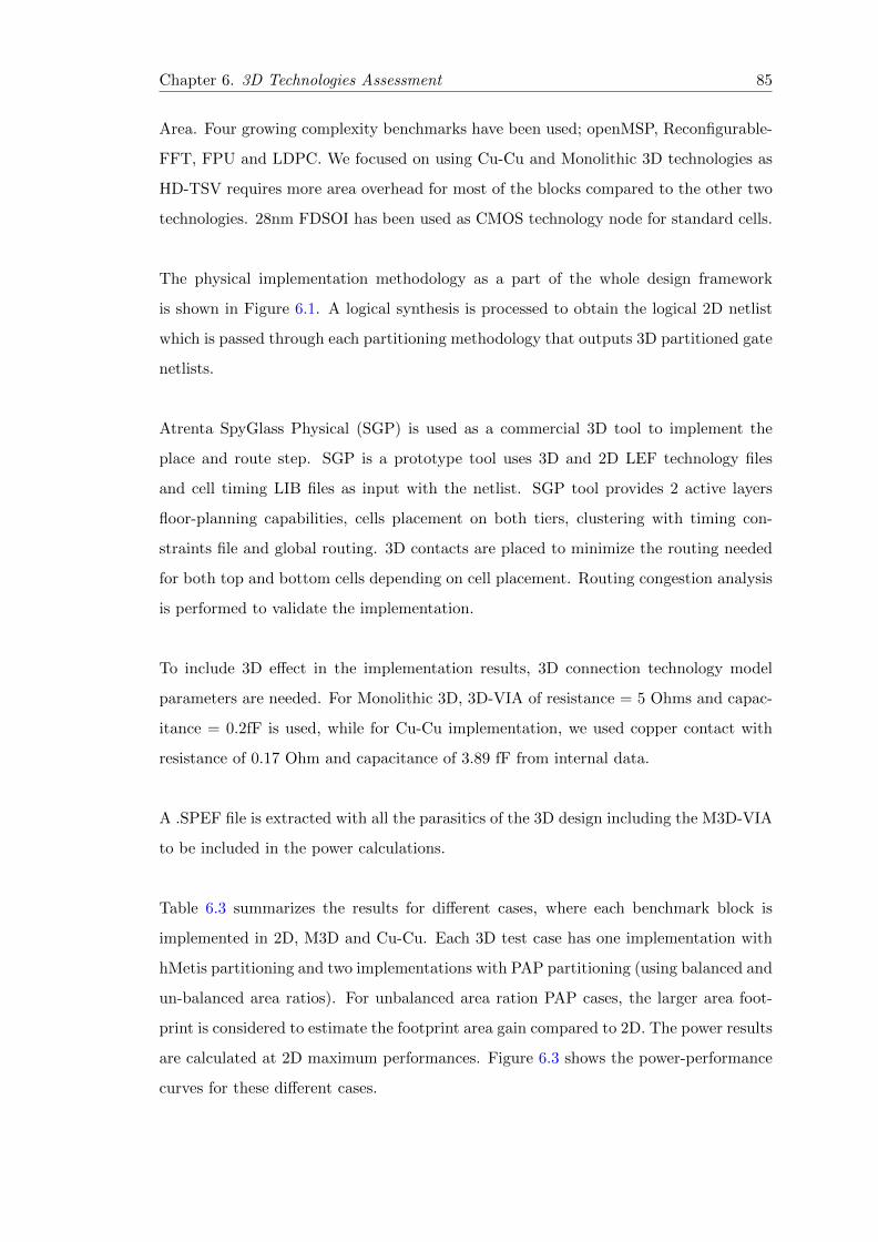
Chapter 6. 3D Technologies Assessment 85
Area. Four growing complexity benchmarks have been used; openMSP, Reconfigurable-
FFT, FPU and LDPC. We focused on using Cu-Cu and Monolithic 3D technologies as
HD-TSV requires more area overhead for most of the blocks compared to the other two
technologies. 28nm FDSOI has been used as CMOS technology node for standard cells.
The physical implementation methodology as a part of the whole design framework
is shown in Figure 6.1. A logical synthesis is processed to obtain the logical 2D netlist
which is passed through each partitioning methodology that outputs 3D partitioned gate
netlists.
Atrenta SpyGlass Physical (SGP) is used as a commercial 3D tool to implement the
place and route step. SGP is a prototype tool uses 3D and 2D LEF technology files
and cell timing LIB files as input with the netlist. SGP tool provides 2 active layers
floor-planning capabilities, cells placement on both tiers, clustering with timing con-
straints file and global routing. 3D contacts are placed to minimize the routing needed
for both top and bottom cells depending on cell placement. Routing congestion analysis
is performed to validate the implementation.
To include 3D effect in the implementation results, 3D connection technology model
parameters are needed. For Monolithic 3D, 3D-VIA of resistance = 5 Ohms and capac-
itance = 0.2fF is used, while for Cu-Cu implementation, we used copper contact with
resistance of 0.17 Ohm and capacitance of 3.89 fF from internal data.
A .SPEF file is extracted with all the parasitics of the 3D design including the M3D-VIA
to be included in the power calculations.
Table 6.3 summarizes the results for different cases, where each benchmark block is
implemented in 2D, M3D and Cu-Cu. Each 3D test case has one implementation with
hMetis partitioning and two implementations with PAP partitioning (using balanced and
un-balanced area ratios). For unbalanced area ration PAP cases, the larger area foot-
print is considered to estimate the footprint area gain compared to 2D. The power results
are calculated at 2D maximum performances. Figure 6.3 shows the power-performance
curves for these different cases.
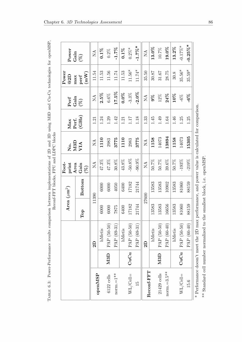
Chapter 6. 3D Technologies Assessment 86
Table
6.3:
Pow
er-P
erfo
rman
cere
sult
sco
mp
aris
onb
etw
een
imple
men
tati
on
sof
2D
an
d3D
usi
ng
M3D
an
dC
u-C
ute
chn
olo
gie
sfo
rop
enM
SP
,R
econ
f-F
FT
blo
cks,
FP
Uan
dL
DP
Cb
lock
s
Are
a(µ
m2)
Foot-
pri
nt
Are
aG
ain
(%)
No.
M3D
VIA
Max
Perf
.(G
Hz)
Perf
Gain
(%)
Pow
er
@2D
max
perf
(mW
)
Pow
er
Gain
(%)
Top
Bott
om
op
en
MS
P2D
1139
0N
AN
A1.
21N
A11
.54
NA
M3D
hM
etis
6000
6000
47.3
%1110
1.24
2.5
%11
.53
0.1
%
6122
cell
sP
AP
(50-
50)
6000
6000
47.3
%29
831.
296.
6%11
.56
0.2%
norm
.=1**
PA
P(6
9-31
)78
7540
5030
.8%
3775
1.42
17.5
%11
.74
-1.7
%
Cu
Cu
hM
etis
6400
6400
43.8
%1110
1.21
0.0
%11
.53
0.1
%
WL
/Cel
l=P
AP
(50-
50)
1718
217
182
-50.
8%29
831.
17-3
.3%
11.5
6*0.
2%*
15P
AP
(69-
31)
2174
421
744
-90.
9%3775
1.18
-2.0
%11
.74*
-1.7
%*
Recon
f-F
FT
2D
2760
0N
AN
A1.
33N
A35
.50
NA
M3D
hM
etis
1358
313
583
50.7
%1158
1.45
9%
30.8
713.0
%
214
29ce
lls
PA
P(5
0-50
)13
583
1358
350
.7%
1407
31.
4912
%31
.67
10.7
%
norm
.=3.5
**P
AP
(60-
40)
1665
610
902
39.6
%13894
1.64
24%
28.7
519.0
%
Cu
Cu
hM
etis
1358
313
583
50.7
%1158
1.46
10%
30.8
13.2
%
WL
/Cel
l=P
AP
(50-
50)
8106
081
060
-193
%14
073
1.25
-6%
35.5
6*-0
.17%
*
15.6
PA
P(6
0-40
)88
159
8815
9-2
19%
15305
1.25
-6%
35.5
9*-0
.25%
*
*P
erfo
rman
ced
oes
n’t
mee
tth
e2D
max
per
form
ance
,an
dp
ower
valu
eis
calc
ula
ted
for
com
par
ison
.
**
Sta
nd
ard
cell
nu
mb
ern
orm
aliz
edto
the
smal
lest
blo
ck,
i.e.
open
MS
P.
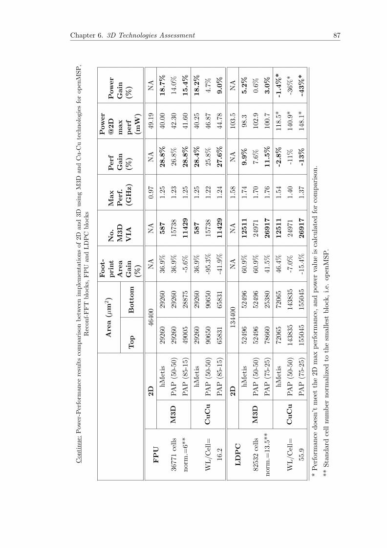
Chapter 6. 3D Technologies Assessment 87
Con
tinu
e:P
ower
-Per
form
ance
resu
lts
com
par
ison
bet
wee
nim
ple
men
tati
on
sof
2D
an
d3D
usi
ng
M3D
an
dC
u-C
ute
chn
olo
gie
sfo
rop
enM
SP
,R
econ
f-F
FT
blo
cks,
FP
Uan
dL
DP
Cb
lock
s
Are
a(µ
m2)
Foot-
pri
nt
Are
aG
ain
(%)
No.
M3D
VIA
Max
Perf
.(G
Hz)
Perf
Gain
(%)
Pow
er
@2D
max
perf
(mW
)
Pow
er
Gain
(%)
Top
Bott
om
FP
U2D
4640
0N
AN
A0.
97N
A49
.19
NA
M3D
hM
etis
2926
029
260
36.9
%587
1.25
28.8
%40
.00
18.7
%
367
71ce
lls
PA
P(5
0-50
)29
260
2926
036
.9%
1573
81.
2326
.8%
42.3
014
.0%
nor
m.=
6**
PA
P(8
5-15
)49
005
2887
5-5
.6%
11429
1.25
28.8
%41
.60
15.4
%
Cu
Cu
hM
etis
2926
029
260
36.9
%587
1.25
28.4
%40
.25
18.2
%
WL
/C
ell=
PA
P(5
0-50
)90
650
9065
0-9
5.3%
1573
81.
2225
.8%
46.8
74.
7%
16.2
PA
P(8
5-15
)65
831
6583
1-4
1.9%
11429
1.24
27.6
%44
.78
9.0
%
LD
PC
2D
1344
00N
AN
A1.
58N
A10
3.5
NA
M3D
hM
etis
5249
652
496
60.9
%12511
1.74
9.9
%98
.35.2
%
825
32ce
lls
PA
P(5
0-50
)52
496
5249
660
.9%
2497
11.
707.
6%10
2.9
0.6%
norm
.=13.
5**
PA
P(7
5-25
)78
660
2538
041
.5%
26917
1.76
11.5
%10
0.7
3.0
%
Cu
Cu
hM
etis
7206
572
065
46.4
%12511
1.54
-2.8
%11
8.5*
-1.4
%*
WL
/C
ell=
PA
P(5
0-50
)14
3835
1438
35-7
.0%
2497
11.
40-1
1%14
0.9*
-36%
*
55.9
PA
P(7
5-25
)15
5045
1550
45-1
5.4%
26917
1.37
-13%
148.
1*-4
3%
*
*P
erfo
rmance
does
n’t
mee
tth
e2D
max
per
form
ance
,an
dp
ower
valu
eis
calc
ula
ted
for
com
par
ison
.
**S
tan
dar
dce
llnu
mb
ern
orm
ali
zed
toth
esm
alle
stb
lock
,i.
e.op
enM
SP
.
Chapter 6. 3D Technologies Assessment 88
(a) (b)
(c) (d)
Figure 6.3: Power-Performance for 2D and 3D using M3D and Cu-Cu technologiesfor (a) openMSP, (b) Reconf-FFT, (c) FPU and (d) LDPC blocks.
A full discussion of the results is mentioned below from three different perspectives: (i)
3D Technology comparison, (ii) Partitioning comparison and (iii) Block Type compari-
son.
6.4.1 Discussion I: 3D Technology Results Comparison
Figure 6.3 shows that going into M3D provides best PPA whatever the block type and
complexity with up to 28.8% higher performance and 45% reduced power and 50.7%
reduced area compared to 2D IC. On the other hand, even if Cu-Cu cannot afford such
high gains, it appears that for FPU block it provides 28.4% better performance, 18.2%
reduced power and 36.9% reduced area compared to 2D, with -0.4% less performance
and -0.5% reduced power and no area waste compared to M3D.
For small block and wire dominated, results show that Cu-Cu is not suitable for 3D
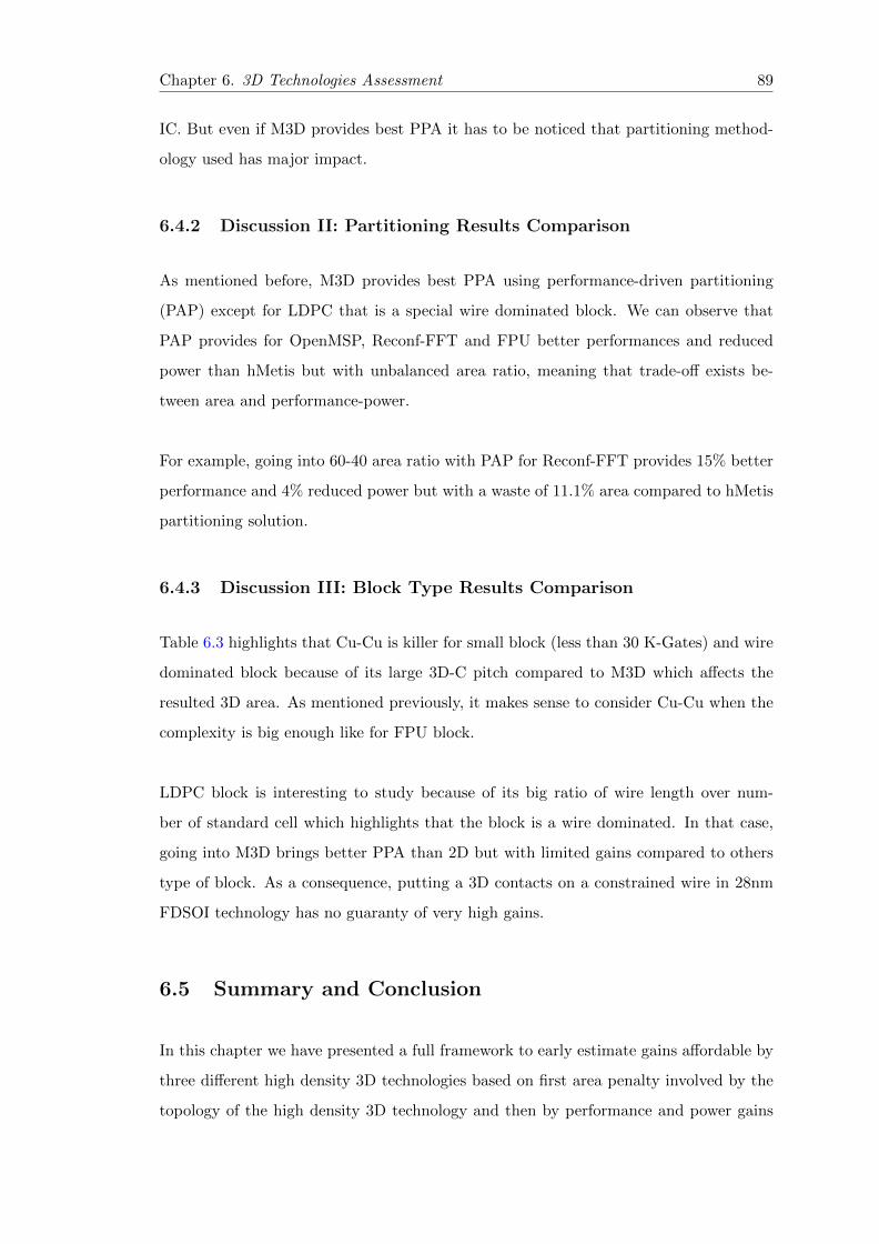
Chapter 6. 3D Technologies Assessment 89
IC. But even if M3D provides best PPA it has to be noticed that partitioning method-
ology used has major impact.
6.4.2 Discussion II: Partitioning Results Comparison
As mentioned before, M3D provides best PPA using performance-driven partitioning
(PAP) except for LDPC that is a special wire dominated block. We can observe that
PAP provides for OpenMSP, Reconf-FFT and FPU better performances and reduced
power than hMetis but with unbalanced area ratio, meaning that trade-off exists be-
tween area and performance-power.
For example, going into 60-40 area ratio with PAP for Reconf-FFT provides 15% better
performance and 4% reduced power but with a waste of 11.1% area compared to hMetis
partitioning solution.
6.4.3 Discussion III: Block Type Results Comparison
Table 6.3 highlights that Cu-Cu is killer for small block (less than 30 K-Gates) and wire
dominated block because of its large 3D-C pitch compared to M3D which affects the
resulted 3D area. As mentioned previously, it makes sense to consider Cu-Cu when the
complexity is big enough like for FPU block.
LDPC block is interesting to study because of its big ratio of wire length over num-
ber of standard cell which highlights that the block is a wire dominated. In that case,
going into M3D brings better PPA than 2D but with limited gains compared to others
type of block. As a consequence, putting a 3D contacts on a constrained wire in 28nm
FDSOI technology has no guaranty of very high gains.
6.5 Summary and Conclusion
In this chapter we have presented a full framework to early estimate gains affordable by
three different high density 3D technologies based on first area penalty involved by the
topology of the high density 3D technology and then by performance and power gains
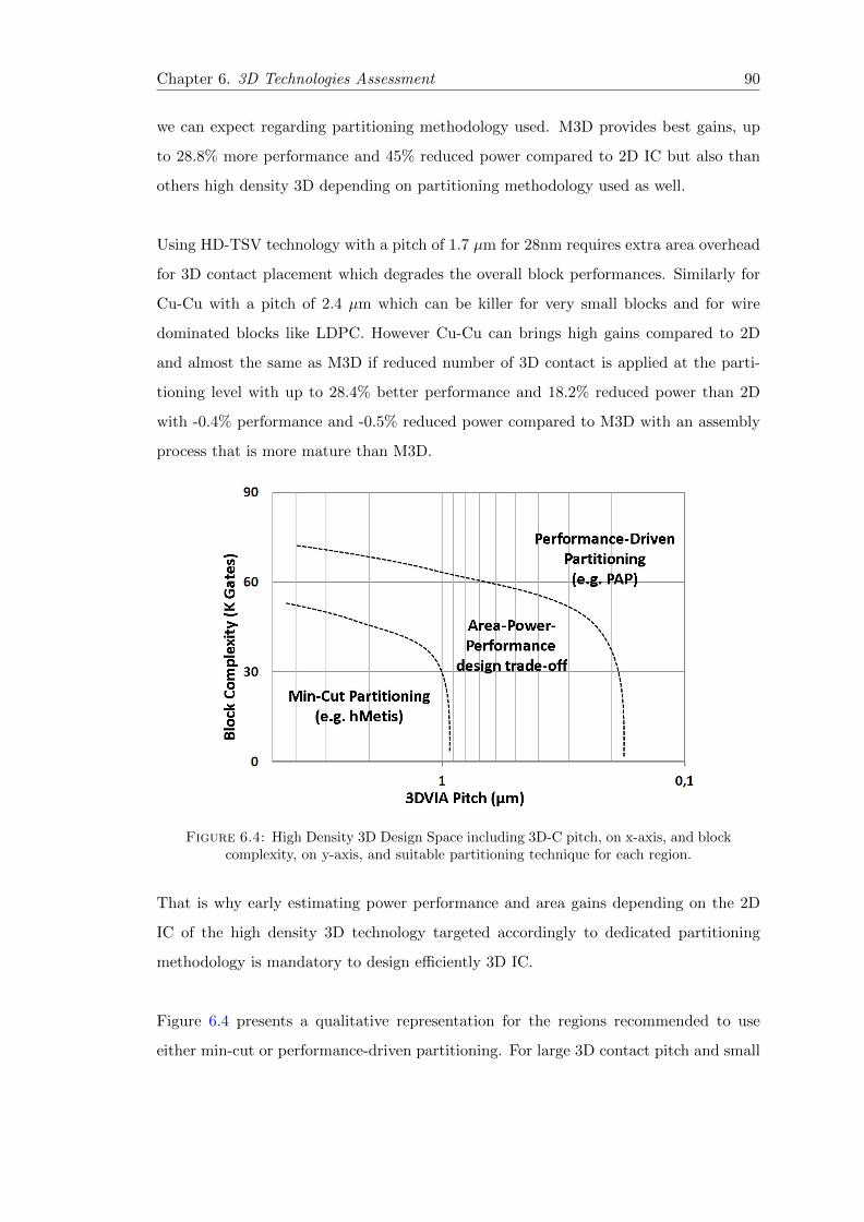
Chapter 6. 3D Technologies Assessment 90
we can expect regarding partitioning methodology used. M3D provides best gains, up
to 28.8% more performance and 45% reduced power compared to 2D IC but also than
others high density 3D depending on partitioning methodology used as well.
Using HD-TSV technology with a pitch of 1.7 µm for 28nm requires extra area overhead
for 3D contact placement which degrades the overall block performances. Similarly for
Cu-Cu with a pitch of 2.4 µm which can be killer for very small blocks and for wire
dominated blocks like LDPC. However Cu-Cu can brings high gains compared to 2D
and almost the same as M3D if reduced number of 3D contact is applied at the parti-
tioning level with up to 28.4% better performance and 18.2% reduced power than 2D
with -0.4% performance and -0.5% reduced power compared to M3D with an assembly
process that is more mature than M3D.
Figure 6.4: High Density 3D Design Space including 3D-C pitch, on x-axis, and blockcomplexity, on y-axis, and suitable partitioning technique for each region.
That is why early estimating power performance and area gains depending on the 2D
IC of the high density 3D technology targeted accordingly to dedicated partitioning
methodology is mandatory to design efficiently 3D IC.
Figure 6.4 presents a qualitative representation for the regions recommended to use
either min-cut or performance-driven partitioning. For large 3D contact pitch and small

Chapter 6. 3D Technologies Assessment 91
blocks, min-cut algorithm is mandatory to minimize the number of 3D contact and lim-
its 3D contact area overhead. As the 3D contact pitch decreases and the block area
increases, performance-driven partitioning becomes more needed to increase 3D overall
performances with no constraints on number of 3D contact.
Chapter 7
Conclusion and Perspective
7.1 Summary and Conclusion
As we have discussed, More’s scaling becomes more and more complex due to increas-
ing technology limitations, where parasitics of the interconnects (i.e. Back-End-of-Line
(BEOL)) increases significantly compared to that of transistors (i.e. the Front-End-of-
Line). One way to decrease the effect of BEOL is by stacking die vertically which is
called 3D Integrated Circuits (3D ICs). Thanks to the advanced 3D technologies, size
and pitch of 3D contacts have been decreased which offers a high-density integration
capabilities. Through-Silicon-Vias (TSVs) and Copper-to-Copper (CuCu) technologies
achieve 3D contact pitch around 3-10µm. However a new 3D technology called Mono-
lithic 3D (M3D) can scale down the 3D contact pitch to 0.11µm. Monolithic 3D is
a sequential integration technology based on CoolCube process, where a second active
layer is fabricated directly (sequentially) on top of the first layer. This integration tech-
nique gives the capability to use the lithography stepper of the process node which
scales down drastically the size and pitch of 3D contacts. Monolithic 3D contact size
for 28nm technology has nearly the same size of Via2 (via between metal 2 and metal 3).
Monolithic 3D and high-density TSV/CuCu technologies creates new design paradigm
at which we can use such advanced technologies to continue CMOS scaling following
More-Moore trend. In this thesis we explored new design methodologies and technology
assessments for different high density 3D technologies, where a full 3D design space has
92
Conclusion and Perspective 93
been explored based on the following aspects; First creating new M3D design methodol-
ogy which is compatible with 2D conventional place and route sign-off flow, (ii) As each
3D via has a delay/power cost due its resistance and capacitance parasitics, a smart par-
titioning algorithm is needed to cut long wires and maximize the 3D power-performance
gains, and (iii) creating a technology assessment framework to evalute different techno-
logical parameters from a design perspective.
Chapter 2 explores the design space for high density 3D technologies, showing different
3D technology varieties where each 3D technology can be used for a different application.
The full 3D design space consists in three main aspects: 3D technologies, partitioning
granularity and 3D CAD tools. First a suitable 3D technology is selected depending
on the application. We have discussed TSV, CuCu and M3D technologies to show the
advantages and limitations of each technology. Another important aspect is the parti-
tioning granularity which determines how to distribute a design into different 3D stacked
layers. In this thesis, our focus was on fine-grain partitioning, meaning gate-level cell-on-
cell and transistor-level integrations. The last aspect is 3D CAD tools which are needed
to perform the whole 3D cell placement, 3D via placement, 3D routing, 3D timing and
power analysis.
Chapters 3 and 4 introduce new design methodologies using M3D. In Chapter 3 we
introduced a new 3D standard cells named 3D Cell-on-Buffer (3DCoB). 3DCoB is based
on splitting 2D cells into a functioning part (cell) stacked over a driving part (buffer).
This approach shows up to 35% performance gain compared to 2D implementation with
a full compatibility with conventional sign-off 2D place and route CAD flow. Addi-
tionally, a low-power multi-VDD technique was applied on 3DCoB at which 21% power
reduction can be obtained with only 2% performance degradation compared to 2D.
In Chapter 4 we explored different partitioning techniques for gate-level cell-on-cell de-
sign approach. Partitioning is the way to distribute standard cells in different tiers.
A physical-aware partitioning methodology has been introduced where we showed two
important aspects for M3D: (i) minimizing number of 3D vias is no longer a constraint
for 3D design, and (ii) unbalancing area ratio between top and bottom tiers improves
power and performance results without paying extra silicon area. Our physical-aware
partitioning methodology showed performance gain up to 24% compared to 2D and
Conclusion and Perspective 94
up to 15% compared to state-of-the-art 3D partitioning technique. Also for the power
we showed that our partitioning reduces power consumption, at iso-performances, up to
22% compared to 2D and up to 12% more compared to other 3D partitioning techniques.
A technology assessment is needed for high-density 3D technologies. Chapters 5 and
6 show full studies of different technological parameters for different 3D technologies. In
Chapter 5 we studied the effect of non-copper Intermediate BEOL (I-BEOL) for M3D
technology. M3D technology requires a temperature of 500-550oC to fabricate the top
active layer sequentially over the bottom one. The conventional BEOL of copper metal
line with ultra-low-k dielectric is unstable at that temperature. Consequently there is a
need to use Tungsten lines with SiO2 dielectric which are stable at that thermal budget.
Tungsten has a 6x resistivity compared to Copper, and using SiO2 dielectric increase
wire capacitance by 1.6x compared to ultra-low-k dielectric. We studied this effect on the
whole power-performance results using different benchmark block. Our study showed
limited impact of using Tungsten/SiO2 I-BEOL where we got a performance degradation
up to 2% and power increase up to 1.5% compared to the Copper/ultra-low-k I-BEOL.
In Chapter 6 we presented a full framework to compare different high-density 3D tech-
nologies to decide which technology is suitable for each design. Different aspects have
been taken into consideration; (i) 3D technology used, (ii) block complexity and µ-
architecture design and (iii) different partitioning techniques. Our framework is based on
first area analysis to calculate the area overhead needed by 3D contacts. Then a power-
performance analysis is performed to show the 3D gains. M3D technology provides up to
28% performance improvement compared to 2D. High-density TSV and CuCu provide
bigger 3D contacts compared to M3D. Consequently using TSV and CuCu technologies
require extra area overhead to insert 3D contacts. This extra area overhead degrade
significantly power-performance-area results and can be killer for very small blocks or
wire-dominant blocks like LDPC. Therefore a min-cut partitioning technique is needed
for TSV and CuCu technologies to minimize number of 3D contacts.
As an overview, the main guidelines for designing using high density 3D technologies
can be summarizes as:
Conclusion and Perspective 95
1. Minimizing number for 3D-VIA is no longer a limitation for Monolithic 3D tech-
nology.
2. New 3D standard cell approaches can be achieved such as 3D cell-on-buffer to
provide better power-performance results.
3. 3D unbalanced area ratio blocks can provide better power-performance results with
no extra silicon usage.
4. Physical-aware partitioning methodology is needed to increase 3D PPA gains.
5. Technology assessment framework is needed to evaluate different technology pa-
rameters specially for Monolithic 3D.
7.2 Perspectives and Future work
7.2.1 Architecture-Level Partitioning
High density 3D technologies afford the capabilities of fine-grain integration; cell-on-cell
and transistor-on-transistor which requires a fine-grain ‘gate-level’ partitioning tech-
niques. In Chapter 4, gate-level partitioning algorithms have been discussed with the
introduction of a physical-aware un-balanced area-ratio partitioning methodology. How-
ever, coarse-grain ‘Architecture-level’ partitioning is still needed for TSV and Cu-Cu
technologies.
Similar to gate-level partitioning, architecture-level partitioning needs to be efficient
in order to increase the power-performance 3D gains. Appendix A presents simulation
framework and results for a case study of architecture-level partitioning for a 3D neural
cliques network. The different partitioning configurations of a 3D neural clique network
are evaluated to show the effect in terms of interconnects power and timing performances.
The simulation results show that different partitioning lead to different power and per-
formance 3D gains compared to 2D. Total wire length gain in 3D compared to 2D varies
from 25% up to 45% depending on the partitioning configuration. Similarly for RC
delay gain which varies from 45% up to 72% compared to 2D depending as well on
Conclusion and Perspective 96
the partitioning configuration. These results show the importance of partitioning in
architecture-level grain.
7.2.2 Congestion Analysis for Decreasing Number of Metal Layers
Generally, one of the main advantages of 3D technologies is footprint area reduction. By
decreasing area, the space allowed for metal routing decreases which can create routing
congestion. Moreover, Monolithic 3D technology affords limited number of metal layers
on the bottom tier, while the full metal stack is kept for the top tier. Thus studying
congestion analysis is crucial for Monolithic 3D technology using different number of
metal layers to know the minimum number of bottom metal layers after which the
congestion increases and becomes impossible to implement the design.
7.2.3 3D Thermal Analysis and PDN design
Thermal analysis has been always one of the main questions raised for 3D technolo-
gies. As stacking more tiers, the power density increases and the thermal dissipation
starts to be more difficult. Power Distribution Network (PDN) design is as well im-
portant aspect for 3D IC, especially by using high-density 3D technologies. PDN is
needed to provide voltage supply to the different stacked tiers, however the 3D contacts
(TSV, CuCu contacts or M3DVIA) has an IR voltage drop due to its parasitics. An IR
drop analysis is needed to design the 3D PDN with the awareness of the thermal impact.
PDN design with thermal analysis for Monothlic 3D has been studied and presented
in [56, 57]. The work in [56] shows the capability of using the metal lines of the PDN
as a cooling factor and reduce the thermal effect, while [57] presents PDN design guide-
lines for M3D taking into consideration total wire length, number of M3D-Vias, routing
congestion, IR drop and thermal effect of PDN. Thermal compact models have been
introduced in [58, 59], where [58] introduces a thermal model for face-to-back and face-
to-face 3D while [59] focuses on Monolithic 3D technology with introducing thermal 3D
floorplanning for M3D.
Conclusion and Perspective 97
However more studies are needed to illustrate the effect of non-conventional Intermedi-
ate BEOL (Tungsten metal line with SiO2 dielectric) on the PDN design including IR
drop analysis and thermal impact.
7.2.4 Further Aspects
The 3D design space is huge and there are even more aspects to be explored. Below we
mention briefly some of these points:
• Cost and yield analysis for designing using high-density 3D technology.
• Including thermal analysis into the design framework, to create a thermal-aware
partitioning methodology for M3D technology.
• Exploring the design methodologies by applying 3D Design for Testability (DFT)
and 3D Design for Manufacturability (DFM).
• Exploring the design and implementation of memories using M3D technology.
• Studying the effect of low-thermal budget (500oC) on the top active layer for M3D
technology.
• Studying other advanced 3D technologies, such as 3D carbon nano-tubes.
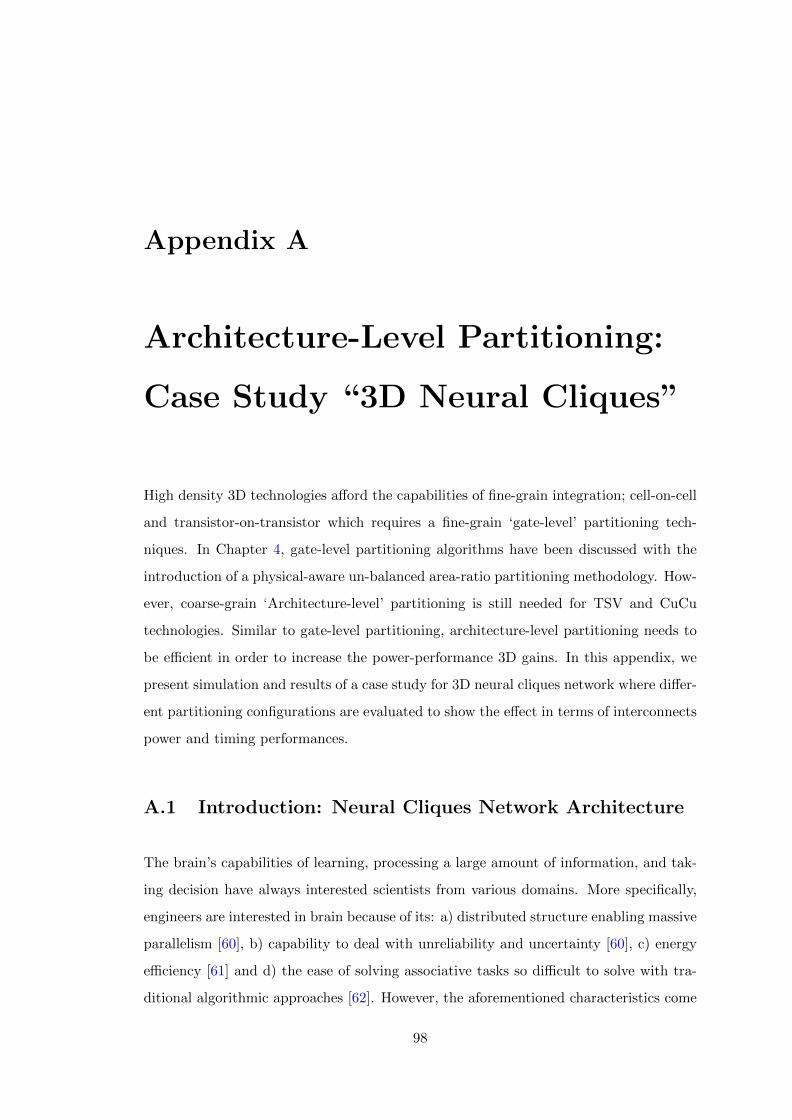
Appendix A
Architecture-Level Partitioning:
Case Study “3D Neural Cliques”
High density 3D technologies afford the capabilities of fine-grain integration; cell-on-cell
and transistor-on-transistor which requires a fine-grain ‘gate-level’ partitioning tech-
niques. In Chapter 4, gate-level partitioning algorithms have been discussed with the
introduction of a physical-aware un-balanced area-ratio partitioning methodology. How-
ever, coarse-grain ‘Architecture-level’ partitioning is still needed for TSV and CuCu
technologies. Similar to gate-level partitioning, architecture-level partitioning needs to
be efficient in order to increase the power-performance 3D gains. In this appendix, we
present simulation and results of a case study for 3D neural cliques network where differ-
ent partitioning configurations are evaluated to show the effect in terms of interconnects
power and timing performances.
A.1 Introduction: Neural Cliques Network Architecture
The brain’s capabilities of learning, processing a large amount of information, and tak-
ing decision have always interested scientists from various domains. More specifically,
engineers are interested in brain because of its: a) distributed structure enabling massive
parallelism [60], b) capability to deal with unreliability and uncertainty [60], c) energy
efficiency [61] and d) the ease of solving associative tasks so difficult to solve with tra-
ditional algorithmic approaches [62]. However, the aforementioned characteristics come
98
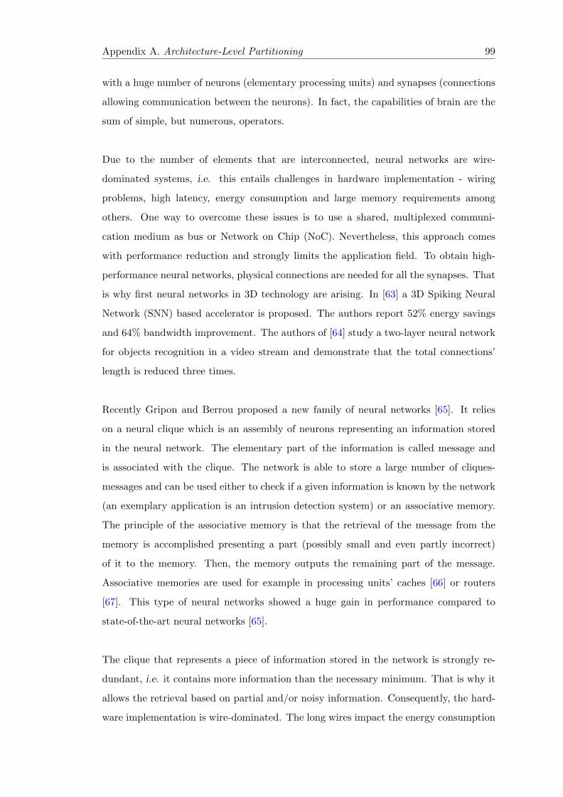
Appendix A. Architecture-Level Partitioning 99
with a huge number of neurons (elementary processing units) and synapses (connections
allowing communication between the neurons). In fact, the capabilities of brain are the
sum of simple, but numerous, operators.
Due to the number of elements that are interconnected, neural networks are wire-
dominated systems, i.e. this entails challenges in hardware implementation - wiring
problems, high latency, energy consumption and large memory requirements among
others. One way to overcome these issues is to use a shared, multiplexed communi-
cation medium as bus or Network on Chip (NoC). Nevertheless, this approach comes
with performance reduction and strongly limits the application field. To obtain high-
performance neural networks, physical connections are needed for all the synapses. That
is why first neural networks in 3D technology are arising. In [63] a 3D Spiking Neural
Network (SNN) based accelerator is proposed. The authors report 52% energy savings
and 64% bandwidth improvement. The authors of [64] study a two-layer neural network
for objects recognition in a video stream and demonstrate that the total connections’
length is reduced three times.
Recently Gripon and Berrou proposed a new family of neural networks [65]. It relies
on a neural clique which is an assembly of neurons representing an information stored
in the neural network. The elementary part of the information is called message and
is associated with the clique. The network is able to store a large number of cliques-
messages and can be used either to check if a given information is known by the network
(an exemplary application is an intrusion detection system) or an associative memory.
The principle of the associative memory is that the retrieval of the message from the
memory is accomplished presenting a part (possibly small and even partly incorrect)
of it to the memory. Then, the memory outputs the remaining part of the message.
Associative memories are used for example in processing units’ caches [66] or routers
[67]. This type of neural networks showed a huge gain in performance compared to
state-of-the-art neural networks [65].
The clique that represents a piece of information stored in the network is strongly re-
dundant, i.e. it contains more information than the necessary minimum. That is why it
allows the retrieval based on partial and/or noisy information. Consequently, the hard-
ware implementation is wire-dominated. The long wires impact the energy consumption
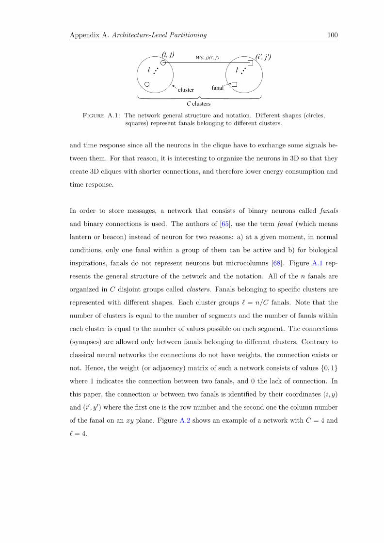
Appendix A. Architecture-Level Partitioning 100
...l ...l
C clusters
(i, j) (i', j')w(i, j)(i', j')
cluster fanal
Figure A.1: The network general structure and notation. Different shapes (circles,squares) represent fanals belonging to different clusters.
and time response since all the neurons in the clique have to exchange some signals be-
tween them. For that reason, it is interesting to organize the neurons in 3D so that they
create 3D cliques with shorter connections, and therefore lower energy consumption and
time response.
In order to store messages, a network that consists of binary neurons called fanals
and binary connections is used. The authors of [65], use the term fanal (which means
lantern or beacon) instead of neuron for two reasons: a) at a given moment, in normal
conditions, only one fanal within a group of them can be active and b) for biological
inspirations, fanals do not represent neurons but microcolumns [68]. Figure A.1 rep-
resents the general structure of the network and the notation. All of the n fanals are
organized in C disjoint groups called clusters. Fanals belonging to specific clusters are
represented with different shapes. Each cluster groups ` = n/C fanals. Note that the
number of clusters is equal to the number of segments and the number of fanals within
each cluster is equal to the number of values possible on each segment. The connections
(synapses) are allowed only between fanals belonging to different clusters. Contrary to
classical neural networks the connections do not have weights, the connection exists or
not. Hence, the weight (or adjacency) matrix of such a network consists of values 0, 1
where 1 indicates the connection between two fanals, and 0 the lack of connection. In
this paper, the connection w between two fanals is identified by their coordinates (i, y)
and (i′, y′) where the first one is the row number and the second one the column number
of the fanal on an xy plane. Figure A.2 shows an example of a network with C = 4 and
` = 4.
Appendix A. Architecture-Level Partitioning 101
x
y12 12
12 12
12 12
12 12
12 12
12 12
12 12
12 12
I II
IIIIV
(i, j)=(1, 1)
(i', j')=(4, 4)
Figure A.2: 2D network example. Different shapes (circles, squares) represent fanalsbelonging to different clusters. Each fanal has 12 synapses to connect to other fanals.
The thick line represents the wire necessary to connect two fanals.
I
IV
II
III
Figure A.3: 3D network (folded network from Figure A.2). Different shapes (circles,squares) represent fanals belonging to different clusters. The thick line represents the
wire necessary to connect two fanals.
A.2 3D neural cliques network architecture
Since the clique is created by interconnecting the fanals from distinct clusters, the wires
span all over the network. Moreover, the performance of the system depends on the
longest wire in the clique since all the fanals activated in the retrieval process exchange
the signals through their connections. Therefore, in such a wire-dominated structure, it
is beneficial to reduce the length of the connections in the clique to reduce the delays and
the energy consumption due to the signals exchanged between the fanals. This can be
obtained by folding the network. Figure A.2 shows an exemplary network. The network
is made of four clusters with four fanals each. Fanals belonging to specific clusters are
represented with different shapes. Each fanal has 12 synapses to provide all the possible
connections. For the simplicity, the length of the wires is measured with the number of
Appendix A. Architecture-Level Partitioning 102
hops between the fanals in terms of the Manhattan distance. In the presented example
the fanal (i, j) = (1, 1) in the cluster I is connected with the fanal (i′, j′) = (4, 4) in the
cluster III. This connection represents the longest possible distance that equals six (the
number of dotted lines that have to be crossed). Figure A.3 shows the same network
after folding. One can see that the clusters II and III are moved to another layer and put
below the clusters I and IV. To realize the connection from Figure A.2, a wire of length
four is used. The connection to the layer below is ensured by the TSV. Depending on the
size and arrangement of the clusters the folding can be done either in x or y direction.
A.3 Simulation model
Since the clique is created by interconnecting the fanals from distinct clusters, the wires
span all over the network. Moreover, the performance of the system depends on the
longest wire in the clique since all the fanals activated in the retrieval process exchange
the signals through their connections. Therefore, in such a wire-dominated structure, it
is beneficial to reduce the length of the connections in the clique to reduce the delays
and the energy consumption due to the signals exchanged between the fanals. This can
be obtained by folding the network as shown in Figure A.3.
To analyze the gains introduced by using 3D technology the lengths of all the possi-
ble connections have to be calculated.
First, the elementary distance between two fanals has to be calculated. This distance
depends on the space occupied by the fanal and all its synapses. The area Af+s occupied
by one fanal and all its synapses is calculated as:
Af+s = Afanal +NsAsynapse (A.1)
where Afanal is the area of the fanal, Asynapse is the area of the synapse, Ns is the
number of the synapses connected to one fanal and is calculated as:
Ns = (C − 1)`. (A.2)
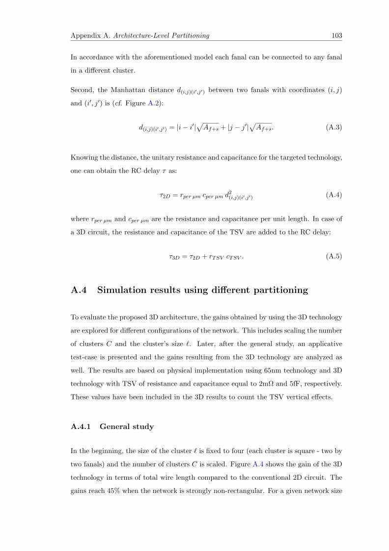
Appendix A. Architecture-Level Partitioning 103
In accordance with the aforementioned model each fanal can be connected to any fanal
in a different cluster.
Second, the Manhattan distance d(i,j)(i′,j′) between two fanals with coordinates (i, j)
and (i′, j′) is (cf. Figure A.2):
d(i,j)(i′,j′) = |i− i′|√Af+s + |j − j′|
√Af+s. (A.3)
Knowing the distance, the unitary resistance and capacitance for the targeted technology,
one can obtain the RC delay τ as:
τ2D = rper µm cper µm d2(i,j)(i′,j′) (A.4)
where rper µm and cper µm are the resistance and capacitance per unit length. In case of
a 3D circuit, the resistance and capacitance of the TSV are added to the RC delay:
τ3D = τ2D + rTSV cTSV . (A.5)
A.4 Simulation results using different partitioning
To evaluate the proposed 3D architecture, the gains obtained by using the 3D technology
are explored for different configurations of the network. This includes scaling the number
of clusters C and the cluster’s size `. Later, after the general study, an applicative
test-case is presented and the gains resulting from the 3D technology are analyzed as
well. The results are based on physical implementation using 65nm technology and 3D
technology with TSV of resistance and capacitance equal to 2mΩ and 5fF, respectively.
These values have been included in the 3D results to count the TSV vertical effects.
A.4.1 General study
In the beginning, the size of the cluster ` is fixed to four (each cluster is square - two by
two fanals) and the number of clusters C is scaled. Figure A.4 shows the gain of the 3D
technology in terms of total wire length compared to the conventional 2D circuit. The
gains reach 45% when the network is strongly non-rectangular. For a given network size
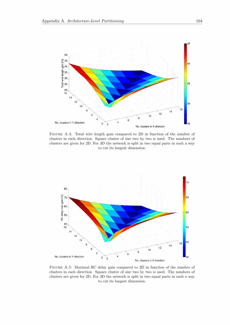
Appendix A. Architecture-Level Partitioning 104
Figure A.4: Total wire length gain compared to 2D in function of the number ofclusters in each direction. Square cluster of size two by two is used. The numbers ofclusters are given for 2D. For 3D the network is split in two equal parts in such a way
to cut its longest dimension.
Figure A.5: Maximal RC delay gain compared to 2D in function of the number ofclusters in each direction. Square cluster of size two by two is used. The numbers ofclusters are given for 2D. For 3D the network is split in two equal parts in such a way
to cut its longest dimension.
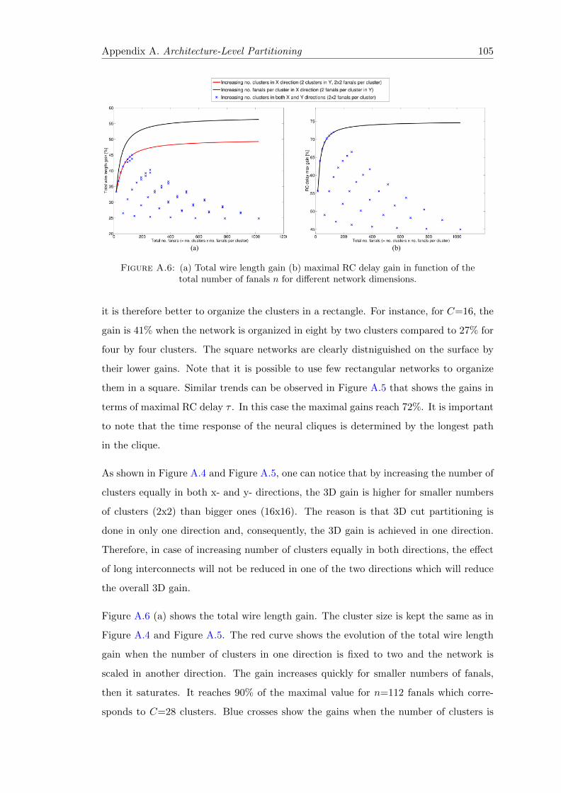
Appendix A. Architecture-Level Partitioning 105
(a) (b)
Figure A.6: (a) Total wire length gain (b) maximal RC delay gain in function of thetotal number of fanals n for different network dimensions.
it is therefore better to organize the clusters in a rectangle. For instance, for C=16, the
gain is 41% when the network is organized in eight by two clusters compared to 27% for
four by four clusters. The square networks are clearly distniguished on the surface by
their lower gains. Note that it is possible to use few rectangular networks to organize
them in a square. Similar trends can be observed in Figure A.5 that shows the gains in
terms of maximal RC delay τ . In this case the maximal gains reach 72%. It is important
to note that the time response of the neural cliques is determined by the longest path
in the clique.
As shown in Figure A.4 and Figure A.5, one can notice that by increasing the number of
clusters equally in both x- and y- directions, the 3D gain is higher for smaller numbers
of clusters (2x2) than bigger ones (16x16). The reason is that 3D cut partitioning is
done in only one direction and, consequently, the 3D gain is achieved in one direction.
Therefore, in case of increasing number of clusters equally in both directions, the effect
of long interconnects will not be reduced in one of the two directions which will reduce
the overall 3D gain.
Figure A.6 (a) shows the total wire length gain. The cluster size is kept the same as in
Figure A.4 and Figure A.5. The red curve shows the evolution of the total wire length
gain when the number of clusters in one direction is fixed to two and the network is
scaled in another direction. The gain increases quickly for smaller numbers of fanals,
then it saturates. It reaches 90% of the maximal value for n=112 fanals which corre-
sponds to C=28 clusters. Blue crosses show the gains when the number of clusters is
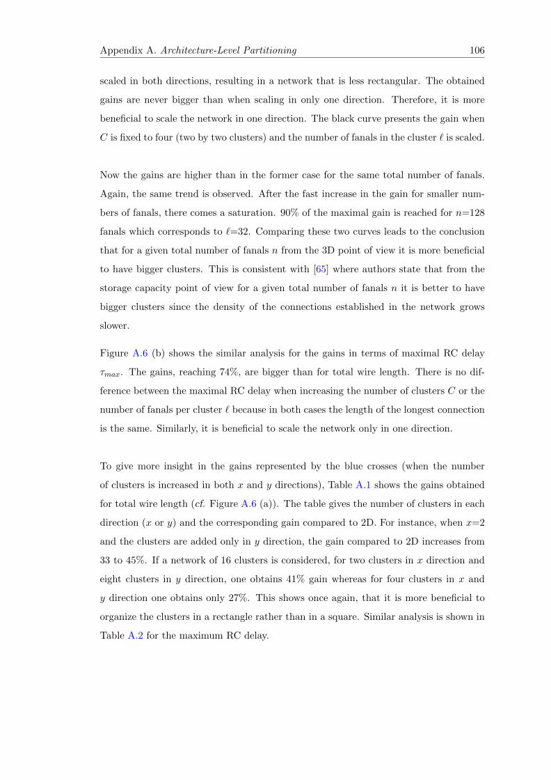
Appendix A. Architecture-Level Partitioning 106
scaled in both directions, resulting in a network that is less rectangular. The obtained
gains are never bigger than when scaling in only one direction. Therefore, it is more
beneficial to scale the network in one direction. The black curve presents the gain when
C is fixed to four (two by two clusters) and the number of fanals in the cluster ` is scaled.
Now the gains are higher than in the former case for the same total number of fanals.
Again, the same trend is observed. After the fast increase in the gain for smaller num-
bers of fanals, there comes a saturation. 90% of the maximal gain is reached for n=128
fanals which corresponds to `=32. Comparing these two curves leads to the conclusion
that for a given total number of fanals n from the 3D point of view it is more beneficial
to have bigger clusters. This is consistent with [65] where authors state that from the
storage capacity point of view for a given total number of fanals n it is better to have
bigger clusters since the density of the connections established in the network grows
slower.
Figure A.6 (b) shows the similar analysis for the gains in terms of maximal RC delay
τmax. The gains, reaching 74%, are bigger than for total wire length. There is no dif-
ference between the maximal RC delay when increasing the number of clusters C or the
number of fanals per cluster ` because in both cases the length of the longest connection
is the same. Similarly, it is beneficial to scale the network only in one direction.
To give more insight in the gains represented by the blue crosses (when the number
of clusters is increased in both x and y directions), Table A.1 shows the gains obtained
for total wire length (cf. Figure A.6 (a)). The table gives the number of clusters in each
direction (x or y) and the corresponding gain compared to 2D. For instance, when x=2
and the clusters are added only in y direction, the gain compared to 2D increases from
33 to 45%. If a network of 16 clusters is considered, for two clusters in x direction and
eight clusters in y direction, one obtains 41% gain whereas for four clusters in x and
y direction one obtains only 27%. This shows once again, that it is more beneficial to
organize the clusters in a rectangle rather than in a square. Similar analysis is shown in
Table A.2 for the maximum RC delay.
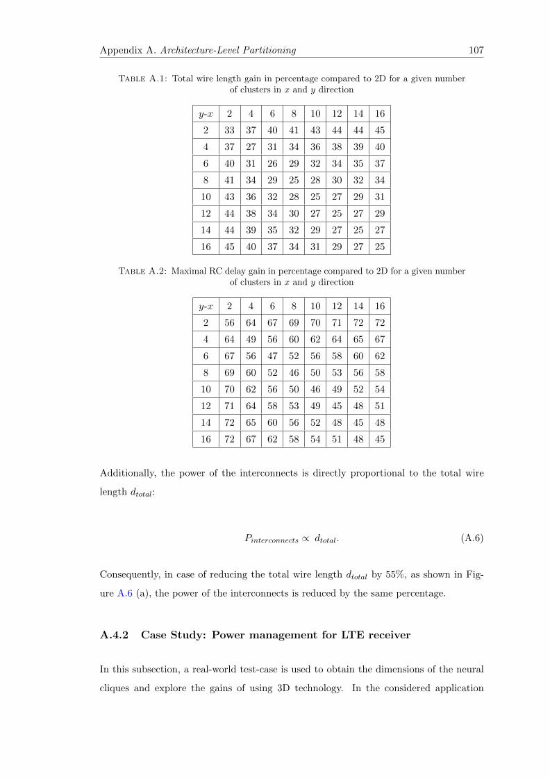
Appendix A. Architecture-Level Partitioning 107
Table A.1: Total wire length gain in percentage compared to 2D for a given numberof clusters in x and y direction
y-x 2 4 6 8 10 12 14 16
2 33 37 40 41 43 44 44 45
4 37 27 31 34 36 38 39 40
6 40 31 26 29 32 34 35 37
8 41 34 29 25 28 30 32 34
10 43 36 32 28 25 27 29 31
12 44 38 34 30 27 25 27 29
14 44 39 35 32 29 27 25 27
16 45 40 37 34 31 29 27 25
Table A.2: Maximal RC delay gain in percentage compared to 2D for a given numberof clusters in x and y direction
y-x 2 4 6 8 10 12 14 16
2 56 64 67 69 70 71 72 72
4 64 49 56 60 62 64 65 67
6 67 56 47 52 56 58 60 62
8 69 60 52 46 50 53 56 58
10 70 62 56 50 46 49 52 54
12 71 64 58 53 49 45 48 51
14 72 65 60 56 52 48 45 48
16 72 67 62 58 54 51 48 45
Additionally, the power of the interconnects is directly proportional to the total wire
length dtotal:
Pinterconnects ∝ dtotal. (A.6)
Consequently, in case of reducing the total wire length dtotal by 55%, as shown in Fig-
ure A.6 (a), the power of the interconnects is reduced by the same percentage.
A.4.2 Case Study: Power management for LTE receiver
In this subsection, a real-world test-case is used to obtain the dimensions of the neural
cliques and explore the gains of using 3D technology. In the considered application
Appendix A. Architecture-Level Partitioning 108
the time response of neural cliques is of first importance. Therefore, high-performance
communication structure is essential.
The considered test-case is a neural cliques-based power management controller for a
Multiprocessor-System-on-Chip (MPSoC) firstly proposed in [69]. An MPSoC is built
of multiple Processing Elements (PE) that can work in parallel. Each PE or set of PEs
form a Voltage/Frequency Island (VFI), i.e. they work within the same power domain.
The supply voltage Vdd and frequency f are set by dedicated switching circuits allowing
Dynamic Voltage and Frequency Scaling (DVFS). By decreasing the speed of the PEs
with lower performance requirements the energy consumption is reduced. The controller
decides on (Vdd, f), or power modes, based on latency constraint, current workload and
temperature among others.
Nowadays, DVFS switching circuits allow switching between two different power modes
in time of the order of tens of nanoseconds [70, 71, 72]. It has been shown in [73] that
providing a controller with time response of the same order of magnitude as DVFS
switching circuits, allows for 60% energy savings compared to 38% in case of a controller
with time response of some µs. That is why neural cliques with high-performance
connections for all the synapses need to be used so that the power management controller
does not limit the power management reactivity.
Here, MAGALI MPSoC platform is considered [74]. The application mapped on the
platform is the LTE receiver [75]. Six PEs are used in the test-case, each PE can
choose from 256 frequencies. The speed of each processor is determined by a global
latency constraint and an operating mode offering different data rates. The global
latency constraint has 51 possible values, there are 5 different operating modes. Based
on the optimization problem defined in [73], the frequencies corresponding to each of
the possible latency and operating mode combination are obtained. Then, neural cliques
are used to store messages containing all the latency and operating mode combinations
and the associated six frequencies. During the system operation, latency and operating
mode are input to the network and the corresponding frequencies are retrieved. These
frequencies are applied to PEs by the DVFS actuators (the DVFS actuator is able
to adjust the necessary Vdd upon the given frequency). Additionally, in each message
a global estimation of the energy consumed by all the PEs is included. Thanks to
that, when the energy consumption is the main constraint (e.g. low battery level), the
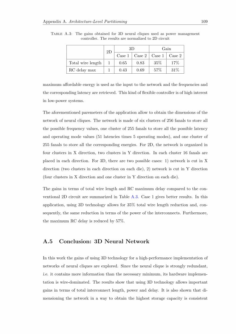
Appendix A. Architecture-Level Partitioning 109
Table A.3: The gains obtained for 3D neural cliques used as power managementcontroller. The results are normalized to 2D circuit
2D3D Gain
Case 1 Case 2 Case 1 Case 2
Total wire length 1 0.65 0.83 35% 17%
RC delay max 1 0.43 0.69 57% 31%
maximum affordable energy is used as the input to the network and the frequencies and
the corresponding latency are retrieved. This kind of flexible controller is of high interest
in low-power systems.
The aforementioned paremeters of the application allow to obtain the dimensions of the
network of neural cliques. The network is made of six clusters of 256 fanals to store all
the possible frequency values, one cluster of 255 fanals to store all the possible latency
and operating mode values (51 latencies times 5 operating modes), and one cluster of
255 fanals to store all the corresponding energies. For 2D, the network is organized in
four clusters in X direction, two clusters in Y direction. In each cluster 16 fanals are
placed in each direction. For 3D, there are two possible cases: 1) network is cut in X
direction (two clusters in each direction on each die), 2) network is cut in Y direction
(four clusters in X direction and one cluster in Y direction on each die).
The gains in terms of total wire length and RC maximum delay compared to the con-
ventional 2D circuit are summarized in Table A.3. Case 1 gives better results. In this
application, using 3D technology allows for 35% total wire length reduction and, con-
sequently, the same reduction in terms of the power of the interconnects. Furthermore,
the maximum RC delay is reduced by 57%.
A.5 Conclusion: 3D Neural Network
In this work the gains of using 3D technology for a high-performance implementation of
networks of neural cliques are explored. Since the neural clique is strongly redundant,
i.e. it contains more information than the necessary minimum, its hardware implemen-
tation is wire-dominated. The results show that using 3D technology allows important
gains in terms of total interconnect length, power and delay. It is also shown that di-
mensioning the network in a way to obtain the highest storage capacity is consistent

Appendix A. Architecture-Level Partitioning 110
with dimensioning the network in a way to obtain the maximal gains coming from 3D
technology. This means that optimizing the gains coming from the theoretical model
and hardware 3D implementation is not contradictory.
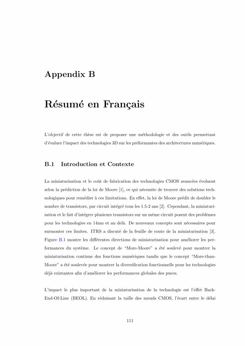
Appendix B
Resume en Francais
L’objectif de cette these est de proposer une methodologie et des outils permettant
d’evaluer l’impact des technologies 3D sur les preformantes des architectures numeriques.
B.1 Introduction et Contexte
La miniaturisation et le cout de fabrication des technologies CMOS avancees evoluent
selon la prediction de la loi de Moore [1], ce qui necessite de trouver des solutions tech-
nologiques pour remedier a ces limitations. En effet, la loi de Moore predit de doubler le
nombre de transistors, par circuit integre tous les 1.5-2 ans [2]. Cependant, la miniaturi-
sation et le fait d’integrer plusieurs transistors sur un meme circuit posent des problemes
pour les technologies en 14nm et au dela. De nouveaux concepts sont necessaires pour
surmonter ces limites. ITRS a discute de la feuille de route de la miniaturisation [3].
Figure B.1 montre les differentes directions de miniaturisation pour ameliorer les per-
formances du systeme. Le concept de “More-Moore” a ete souleve pour montrer la
miniaturisation continue des fonctions numeriques tandis que le concept “More-than-
Moore” a ete soulevee pour montrer la diversification fonctionnelle pour les technologies
deja existantes afin d’ameliorer les performances globales des puces.
L’impact le plus important de la miniaturisation de la technologie est l’effet Back-
End-Of-Line (BEOL). En reduisant la taille des nœuds CMOS, l’ecart entre le delai
111
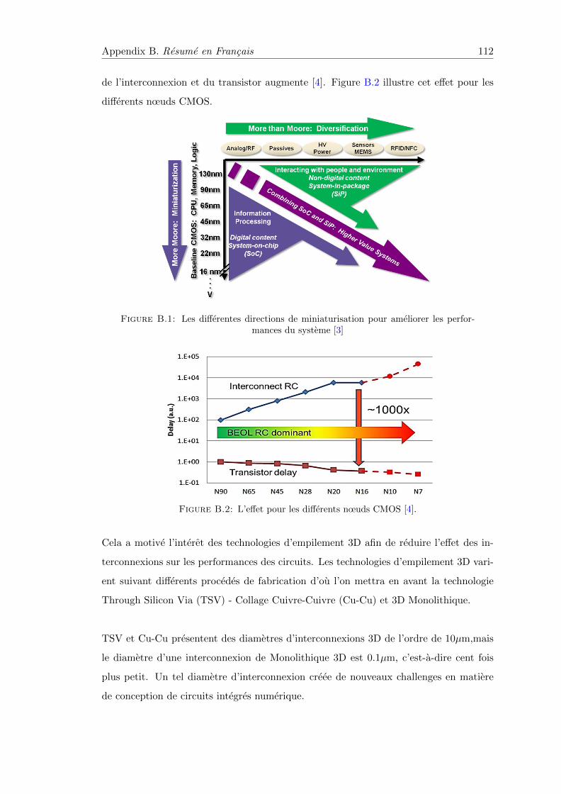
Appendix B. Resume en Francais 112
de l’interconnexion et du transistor augmente [4]. Figure B.2 illustre cet effet pour les
differents nœuds CMOS.
Figure B.1: Les differentes directions de miniaturisation pour ameliorer les perfor-mances du systeme [3]
Figure B.2: L’effet pour les differents nœuds CMOS [4].
Cela a motive l’interet des technologies d’empilement 3D afin de reduire l’effet des in-
terconnexions sur les performances des circuits. Les technologies d’empilement 3D vari-
ent suivant differents procedes de fabrication d’ou l’on mettra en avant la technologie
Through Silicon Via (TSV) - Collage Cuivre-Cuivre (Cu-Cu) et 3D Monolithique.
TSV et Cu-Cu presentent des diametres d’interconnexions 3D de l’ordre de 10µm,mais
le diametre d’une interconnexion de Monolithique 3D est 0.1µm, c’est-a-dire cent fois
plus petit. Un tel diametre d’interconnexion creee de nouveaux challenges en matiere
de conception de circuits integres numerique.
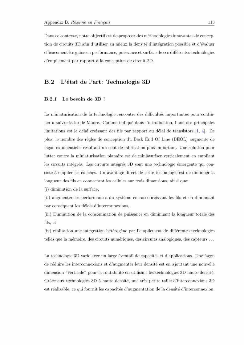
Appendix B. Resume en Francais 113
Dans ce contexte, notre objectif est de proposer des methodologies innovantes de concep-
tion de circuits 3D afin d’utiliser au mieux la densite d’integration possible et d’evaluer
efficacement les gains en performance, puissance et surface de ces differentes technologies
d’empilement par rapport a la conception de circuit 2D.
B.2 L’etat de l’art: Technologie 3D
B.2.1 Le besoin de 3D !
La miniaturisation de la technologie rencontre des difficultes importantes pour contin-
uer a suivre la loi de Moore. Comme indique dans l’introduction, l’une des principales
limitations est le delai croissant des fils par rapport au delai de transistors [1, 4]. De
plus, le nombre des regles de conception du Back End Of Line (BEOL) augmente de
facon exponentielle resultant un cout de fabrication plus important. Une solution pour
lutter contre la miniaturisation planaire est de miniaturiser verticalement en empilant
les circuits integres. Les circuits integres 3D sont une technologie emergente qui con-
siste a empiler les couches. Un avantage direct de cette technologie est de diminuer la
longueur des fils en connectant les cellules sur trois dimensions, ainsi que:
(i) diminution de la surface,
(ii) augmenter les performances du systeme en raccourcissant les fils et en diminuant
par consequent les delais d’interconnexions,
(iii) Diminution de la consommation de puissance en diminuant la longueur totale des
fils, et
(iv) realisation une integration heterogene par l’empilement de differentes technologies
telles que la memoire, des circuits numeriques, des circuits analogiques, des capteurs . . .
La technologie 3D varie avec un large eventail de capacites et d’applications. Une facon
de reduire les interconnexions et d’augmenter leur densite est en ajoutant une nouvelle
dimension “verticale” pour la routabilite en utilisant les technologies 3D haute densite.
Grace aux technologies 3D a haute densite, une tres petite taille d’interconnexions 3D
est realisable, ce qui fournit les capacites d’augmentation de la densite d’interconnexion.
Appendix B. Resume en Francais 114
B.2.2 Spectre de la technologie 3D
B.2.2.1 Schemas d’integration
i. 2.5D/3D Interposer
L’interposer est une etape intermediaire entre un circuit 2D et un circuit purement
3D. Cette technologie est obtenue en ajoutant les differentes pcouches “dies” sur une
couche de silicium appele un interposer [10, 11, 12]. Un interposer peut-etre soit (i)
passif (ii) soit actif.
l’Interposer passif contient seulement des fils qui relient les differentes couches “dies”
sans regions actives, c’est a dire sans transistor. Alors que dans l’interposer actif, la
couche de l’interposer a des composants actifs tels que des memoires tampons ou des
blocs de communication (par exemple, reseau sur puce “NoC”). La figure B.3 montre
un schema-bloc d’un interposer actif. La motivation de la technologie interposer est
de reduire la surface du silicium en divisant la puce en deux puces integrees sur un
interposer qui peut augmenter le rendement, reduire les couts et permettre l’integration
heterogene en ayant differents technologies CMOS pour chaque puce.
Figure B.3: Schematique de l’interposition active
ii. Circuit 3D: face-a-dos et face-a-face
L’integration 3D peut etre soit en face-a-face (face-to-face F2F), soit en face-a-dos (face-
to-back F2B). Dans ce contexte, nous considerons que chaque puce a une face et un
dos, ou la face est le niveau haut de la couche metal et le dos de la puce est le substrat
de silicium. Par consequent, les puces peuvent etre empiles dans une configuration de
face-a-face de tel sorte que les couches metalliques superieures soient en face l’une a
l’autre.
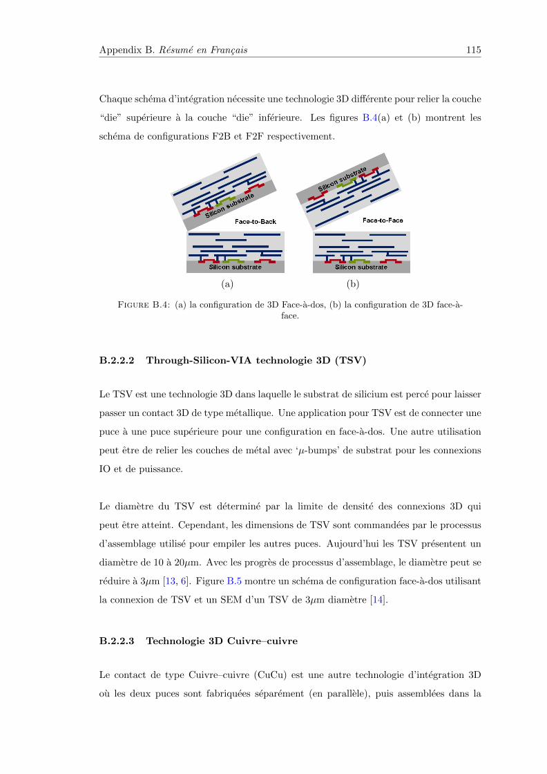
Appendix B. Resume en Francais 115
Chaque schema d’integration necessite une technologie 3D differente pour relier la couche
“die” superieure a la couche “die” inferieure. Les figures B.4(a) et (b) montrent les
schema de configurations F2B et F2F respectivement.
(a) (b)
Figure B.4: (a) la configuration de 3D Face-a-dos, (b) la configuration de 3D face-a-face.
B.2.2.2 Through-Silicon-VIA technologie 3D (TSV)
Le TSV est une technologie 3D dans laquelle le substrat de silicium est perce pour laisser
passer un contact 3D de type metallique. Une application pour TSV est de connecter une
puce a une puce superieure pour une configuration en face-a-dos. Une autre utilisation
peut etre de relier les couches de metal avec ‘µ-bumps’ de substrat pour les connexions
IO et de puissance.
Le diametre du TSV est determine par la limite de densite des connexions 3D qui
peut etre atteint. Cependant, les dimensions de TSV sont commandees par le processus
d’assemblage utilise pour empiler les autres puces. Aujourd’hui les TSV presentent un
diametre de 10 a 20µm. Avec les progres de processus d’assemblage, le diametre peut se
reduire a 3µm [13, 6]. Figure B.5 montre un schema de configuration face-a-dos utilisant
la connexion de TSV et un SEM d’un TSV de 3µm diametre [14].
B.2.2.3 Technologie 3D Cuivre–cuivre
Le contact de type Cuivre–cuivre (CuCu) est une autre technologie d’integration 3D
ou les deux puces sont fabriquees separement (en parallele), puis assemblees dans la
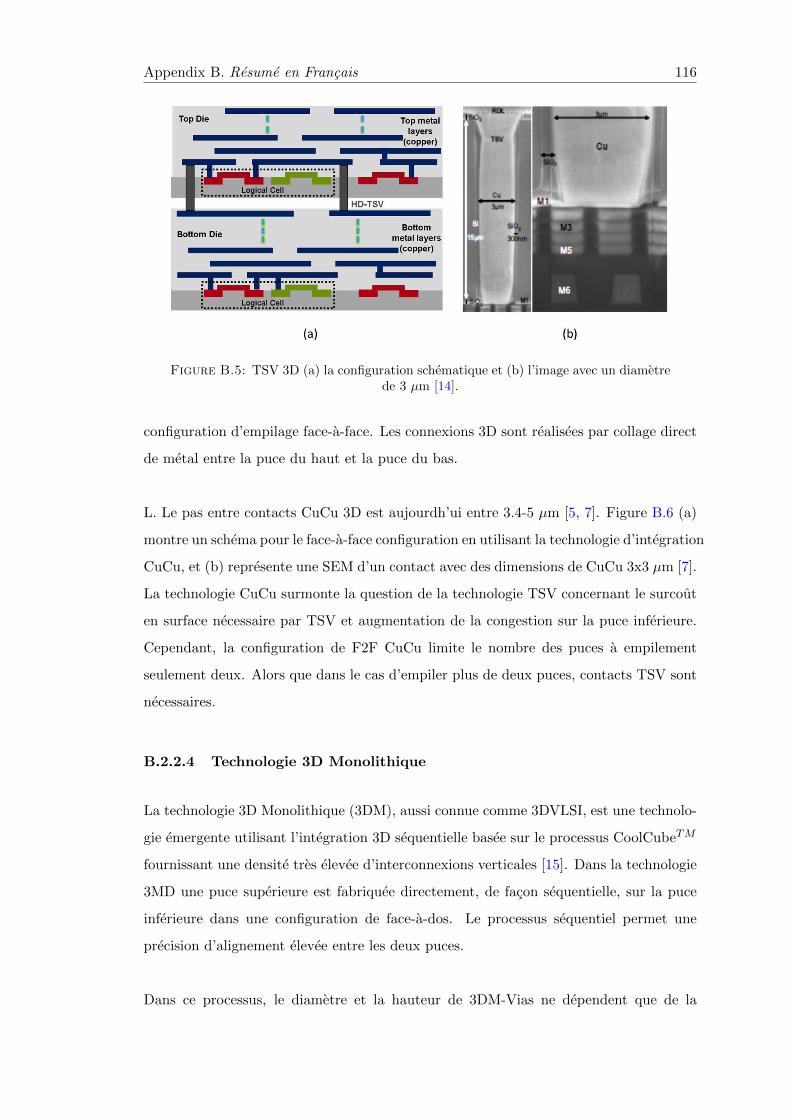
Appendix B. Resume en Francais 116
Figure B.5: TSV 3D (a) la configuration schematique et (b) l’image avec un diametrede 3 µm [14].
configuration d’empilage face-a-face. Les connexions 3D sont realisees par collage direct
de metal entre la puce du haut et la puce du bas.
L. Le pas entre contacts CuCu 3D est aujourdh’ui entre 3.4-5 µm [5, 7]. Figure B.6 (a)
montre un schema pour le face-a-face configuration en utilisant la technologie d’integration
CuCu, et (b) represente une SEM d’un contact avec des dimensions de CuCu 3x3 µm [7].
La technologie CuCu surmonte la question de la technologie TSV concernant le surcout
en surface necessaire par TSV et augmentation de la congestion sur la puce inferieure.
Cependant, la configuration de F2F CuCu limite le nombre des puces a empilement
seulement deux. Alors que dans le cas d’empiler plus de deux puces, contacts TSV sont
necessaires.
B.2.2.4 Technologie 3D Monolithique
La technologie 3D Monolithique (3DM), aussi connue comme 3DVLSI, est une technolo-
gie emergente utilisant l’integration 3D sequentielle basee sur le processus CoolCubeTM
fournissant une densite tres elevee d’interconnexions verticales [15]. Dans la technologie
3MD une puce superieure est fabriquee directement, de facon sequentielle, sur la puce
inferieure dans une configuration de face-a-dos. Le processus sequentiel permet une
precision d’alignement elevee entre les deux puces.
Dans ce processus, le diametre et la hauteur de 3DM-Vias ne dependent que de la
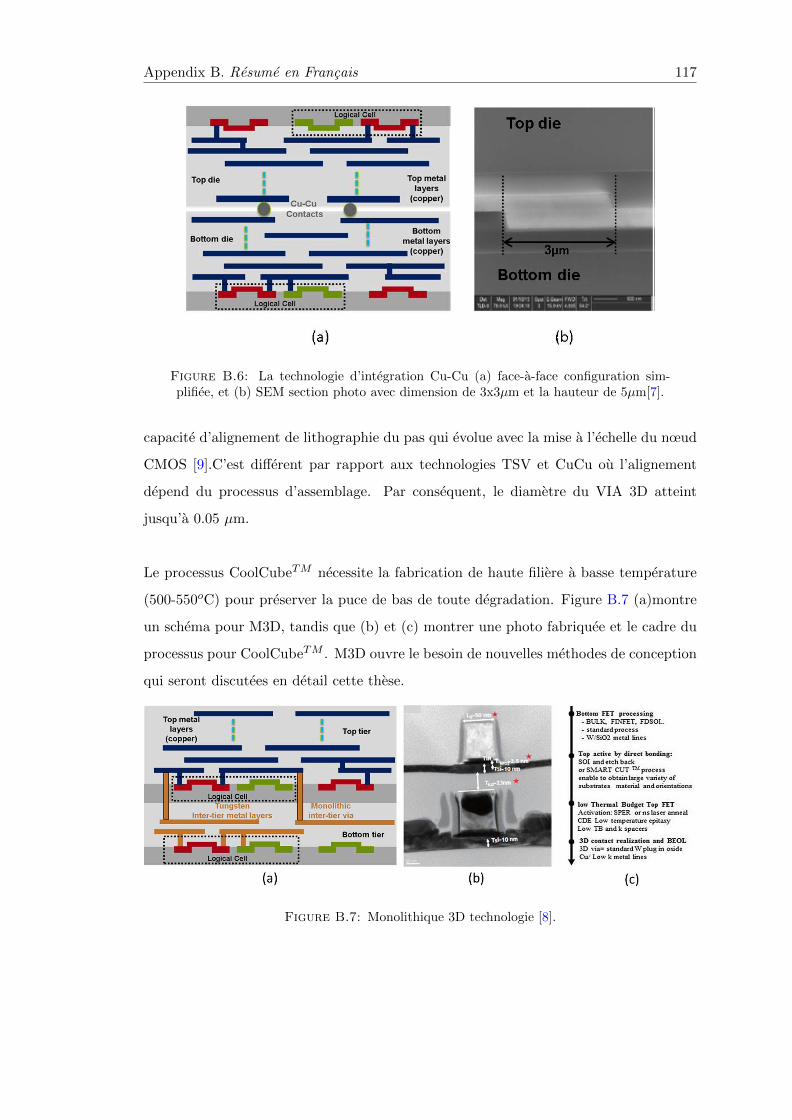
Appendix B. Resume en Francais 117
Figure B.6: La technologie d’integration Cu-Cu (a) face-a-face configuration sim-plifiee, et (b) SEM section photo avec dimension de 3x3µm et la hauteur de 5µm[7].
capacite d’alignement de lithographie du pas qui evolue avec la mise a l’echelle du nœud
CMOS [9].C’est different par rapport aux technologies TSV et CuCu ou l’alignement
depend du processus d’assemblage. Par consequent, le diametre du VIA 3D atteint
jusqu’a 0.05 µm.
Le processus CoolCubeTM necessite la fabrication de haute filiere a basse temperature
(500-550oC) pour preserver la puce de bas de toute degradation. Figure B.7 (a)montre
un schema pour M3D, tandis que (b) et (c) montrer une photo fabriquee et le cadre du
processus pour CoolCubeTM . M3D ouvre le besoin de nouvelles methodes de conception
qui seront discutees en detail cette these.
Figure B.7: Monolithique 3D technologie [8].
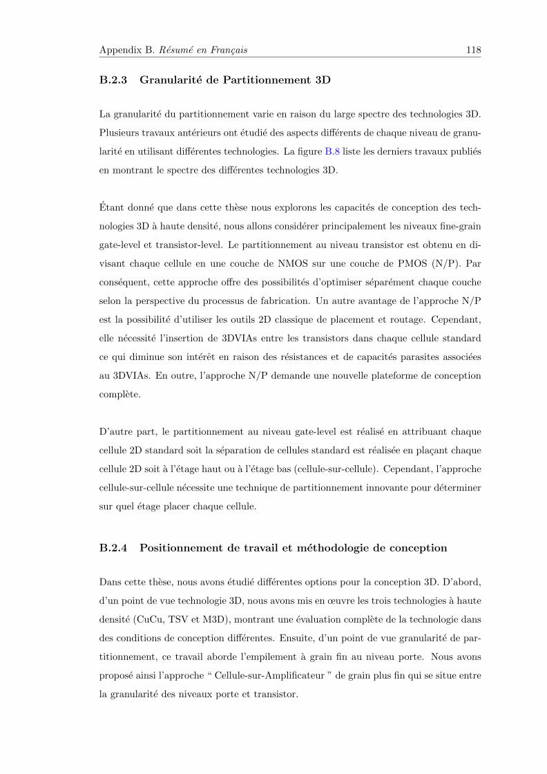
Appendix B. Resume en Francais 118
B.2.3 Granularite de Partitionnement 3D
La granularite du partitionnement varie en raison du large spectre des technologies 3D.
Plusieurs travaux anterieurs ont etudie des aspects differents de chaque niveau de granu-
larite en utilisant differentes technologies. La figure B.8 liste les derniers travaux publies
en montrant le spectre des differentes technologies 3D.
Etant donne que dans cette these nous explorons les capacites de conception des tech-
nologies 3D a haute densite, nous allons considerer principalement les niveaux fine-grain
gate-level et transistor-level. Le partitionnement au niveau transistor est obtenu en di-
visant chaque cellule en une couche de NMOS sur une couche de PMOS (N/P). Par
consequent, cette approche offre des possibilites d’optimiser separement chaque couche
selon la perspective du processus de fabrication. Un autre avantage de l’approche N/P
est la possibilite d’utiliser les outils 2D classique de placement et routage. Cependant,
elle necessite l’insertion de 3DVIAs entre les transistors dans chaque cellule standard
ce qui diminue son interet en raison des resistances et de capacites parasites associees
au 3DVIAs. En outre, l’approche N/P demande une nouvelle plateforme de conception
complete.
D’autre part, le partitionnement au niveau gate-level est realise en attribuant chaque
cellule 2D standard soit la separation de cellules standard est realisee en placant chaque
cellule 2D soit a l’etage haut ou a l’etage bas (cellule-sur-cellule). Cependant, l’approche
cellule-sur-cellule necessite une technique de partitionnement innovante pour determiner
sur quel etage placer chaque cellule.
B.2.4 Positionnement de travail et methodologie de conception
Dans cette these, nous avons etudie differentes options pour la conception 3D. D’abord,
d’un point de vue technologie 3D, nous avons mis en œuvre les trois technologies a haute
densite (CuCu, TSV et M3D), montrant une evaluation complete de la technologie dans
des conditions de conception differentes. Ensuite, d’un point de vue granularite de par-
titionnement, ce travail aborde l’empilement a grain fin au niveau porte. Nous avons
propose ainsi l’approche “ Cellule-sur-Amplificateur ” de grain plus fin qui se situe entre
la granularite des niveaux porte et transistor.
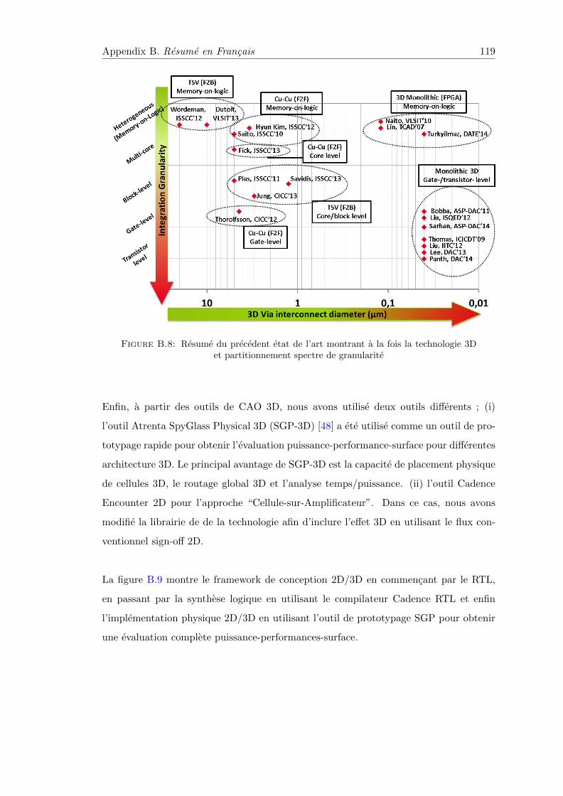
Appendix B. Resume en Francais 119
Figure B.8: Resume du precedent etat de l’art montrant a la fois la technologie 3Det partitionnement spectre de granularite
Enfin, a partir des outils de CAO 3D, nous avons utilise deux outils differents ; (i)
l’outil Atrenta SpyGlass Physical 3D (SGP-3D) [48] a ete utilise comme un outil de pro-
totypage rapide pour obtenir l’evaluation puissance-performance-surface pour differentes
architecture 3D. Le principal avantage de SGP-3D est la capacite de placement physique
de cellules 3D, le routage global 3D et l’analyse temps/puissance. (ii) l’outil Cadence
Encounter 2D pour l’approche “Cellule-sur-Amplificateur”. Dans ce cas, nous avons
modifie la librairie de de la technologie afin d’inclure l’effet 3D en utilisant le flux con-
ventionnel sign-off 2D.
La figure B.9 montre le framework de conception 2D/3D en commencant par le RTL,
en passant par la synthese logique en utilisant le compilateur Cadence RTL et enfin
l’implementation physique 2D/3D en utilisant l’outil de prototypage SGP pour obtenir
une evaluation complete puissance-performances-surface.
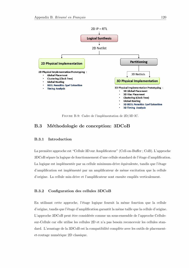
Appendix B. Resume en Francais 120
Figure B.9: Cadre de l’implementation de 2D/3D IC.
B.3 Methodologie de conception: 3DCoB
B.3.1 Introduction
La premiere approche est “Cellule 3D sur Amplificateur” (Cell-on-Buffer ; CoB). L’approche
3DCoB separe la logique de fonctionnement d’une cellule standard de l’etage d’amplification.
La logique est implementee par sa cellule minimum-drive equivalente, tandis que l’etage
d’amplification est implemente par un amplificateur de meme excitation que la cellule
d’origine. La cellule min-drive et l’amplificateur sont ensuite empiles verticalement.
B.3.2 Configuration des cellules 3DCoB
En utilisant cette approche, l’etage logique fournit la meme fonction que la cellule
d’origine, tandis que l’etage d’amplification garantit la meme taille que la cellule d’origine.
L’approche 3DCoB peut etre consideree comme un sous-ensemble de l’approche Cellule-
sur-Cellule car elle utilise les cellules 2D et n’a pas besoin reconcevoir les cellules stan-
dard. L’avantage de la 3DCoB est la compatibilite complete avec les outils de placement-
et-routage numerique 2D classique.
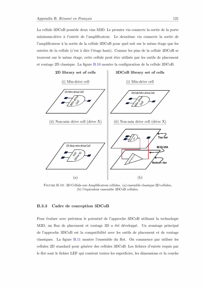
Appendix B. Resume en Francais 121
La cellule 3DCoB possede deux vias M3D. Le premier via connecte la sortie de la porte
minimum-drive a l’entree de l’amplificateur. Le deuxieme via connecte la sortie de
l’amplificateur a la sortie de la cellule 3DCoB pour quel soit sur le meme etage que les
entrees de la cellule (c’est a dire l’etage haut). Comme les pins de la cellule 3DCoB se
trouvent sur le meme etage, cette cellule peut etre utilisee par les outils de placement
et routage 2D classique. La figure B.10 montre la configuration de la cellule 3DCoB.
2D library set of cells 3DCoB library set of cells
(i) Min-drive cell (i) Min-drive cell
(ii) Non-min drive cell (drive X) (ii) Non-min drive cell (drive X)
(a) (b)
Figure B.10: 3D Cellule-sur-Amplificateur cellules. (a) ensemble classique 2D cellules,(b) l’equivalent ensemble 3DCoB cellules.
B.3.3 Cadre de conception 3DCoB
Pour evaluer avec precision le potentiel de l’approche 3DCoB utilisant la technologie
M3D, un flux de placement et routage 3D a ete developpe. Un avantage principal
de l’approche 3DCoB est la compatibilite avec les outils de placement et de routage
classiques. La figure B.11 montre l’ensemble du flot. On commence par utiliser les
cellules 2D standard pour generer des cellules 3DCoB. Les fichiers d’entree requis par
le flot sont le fichier LEF qui contient toutes les superficies, les dimensions et la couche
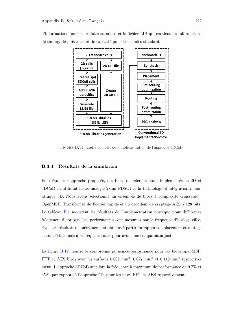
Appendix B. Resume en Francais 122
d’informations pour les cellules standard et le fichier LIB qui contient les informations
de timing, de puissance et de capacite pour les cellules standard.
Figure B.11: Cadre complet de l’implementation de l’approche 3DCoB
B.3.4 Resultats de la simulation
Pour evaluer l’approche proposee, des blocs de reference sont implementes en 2D et
3DCoB en utilisant la technologie 28nm FDSOI et la technologie d’integration mono-
lithique 3D. Nous avons selectionne un ensemble de blocs a complexite croissante :
OpenMSP, Transformee de Fourier rapide et un decodeur de cryptage AES a 128 bits.
Le tableau B.1 montrent les resultats de l’implementation physique pour differentes
frequences d’horloge. Les performances sont mesurees par la frequence d’horloge effec-
tive. Les resultats de puissance sont obtenus a partir du rapport de placement et routage
et sont echelonnes a la frequence max pour avoir une comparaison juste.
La figure B.12 montre le compromis puissance-performance pour les blocs openMSP,
FFT et AES blocs avec les surfaces 0.008 mm2, 0.027 mm2 et 0.119 mm2 respective-
ment. L’approche 3DCoB ameliore la frequence a maximum de performance de 9.7% et
35%, par rapport a l’approche 2D, pour les blocs FFT et AES respectivement.
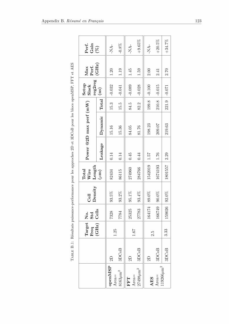
Appendix B. Resume en Francais 123
TableB.1:
Res
ult
ats
pu
issa
nce
-per
form
an
cep
ou
rle
sap
pro
ches
2D
et3D
CoB
pou
rle
sb
locs
op
enM
SP
,F
FT
etA
ES
Targ
et
Fre
q(G
Hz)
No.
Std
Cells
Cell
Den
sity
Tota
lW
ire
Len
gth
(µm
)
Pow
er
@2D
max
perf
(mW
)S
etu
pS
lack
reg2re
g(n
s)
Max
Perf
.(G
Hz)
Perf
.G
ain
(%)
Leakage
Dyn
am
icT
ota
l
op
en
MS
PA
rea=
816
3µm
2
2D
1.25
7328
93.5
%82
434
0.14
15.1
615
.3-0
.032
1.20
-NA
-
3D
CoB
7784
93.2
%86
115
0.14
15.3
615
.5-0
.041
1.19
-0.8
%
FF
TA
rea=
274
98µ
m2
2D
1.67
2532
595
.1%
2749
600.
4584
.05
84.5
-0.0
891.
45-N
A-
3D
CoB
2778
393
.4%
2847
660.
4481
.76
82.2
-0.0
281.
59+
9.65
%
AE
SA
rea=
119
266µ
m2
2D
2.5
1641
7489
.0%
1542
019
1.57
198.
2319
9.8
-0.1
002.
00-N
A-
3D
CoB
1667
4990
.0%
1674
193
1.76
209.
0721
0.8
-0.0
152.
41+
20.5
%
3D
CoB
3.33
1590
2692
.0%
1801
557
2.29
219.
6322
1.9
-0.0
712.
70+
34.7
%
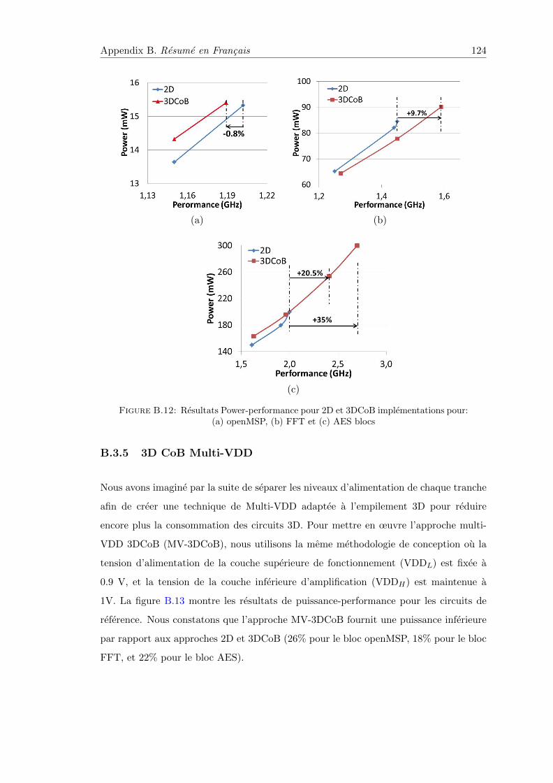
Appendix B. Resume en Francais 124
(a) (b)
(c)
Figure B.12: Resultats Power-performance pour 2D et 3DCoB implementations pour:(a) openMSP, (b) FFT et (c) AES blocs
B.3.5 3D CoB Multi-VDD
Nous avons imagine par la suite de separer les niveaux d’alimentation de chaque tranche
afin de creer une technique de Multi-VDD adaptee a l’empilement 3D pour reduire
encore plus la consommation des circuits 3D. Pour mettre en œuvre l’approche multi-
VDD 3DCoB (MV-3DCoB), nous utilisons la meme methodologie de conception ou la
tension d’alimentation de la couche superieure de fonctionnement (VDDL) est fixee a
0.9 V, et la tension de la couche inferieure d’amplification (VDDH) est maintenue a
1V. La figure B.13 montre les resultats de puissance-performance pour les circuits de
reference. Nous constatons que l’approche MV-3DCoB fournit une puissance inferieure
par rapport aux approches 2D et 3DCoB (26% pour le bloc openMSP, 18% pour le bloc
FFT, et 22% pour le bloc AES).
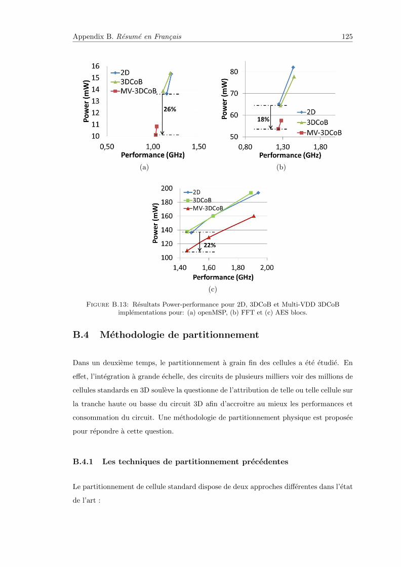
Appendix B. Resume en Francais 125
(a) (b)
(c)
Figure B.13: Resultats Power-performance pour 2D, 3DCoB et Multi-VDD 3DCoBimplementations pour: (a) openMSP, (b) FFT et (c) AES blocs.
B.4 Methodologie de partitionnement
Dans un deuxieme temps, le partitionnement a grain fin des cellules a ete etudie. En
effet, l’integration a grande echelle, des circuits de plusieurs milliers voir des millions de
cellules standards en 3D souleve la questionne de l’attribution de telle ou telle cellule sur
la tranche haute ou basse du circuit 3D afin d’accroıtre au mieux les performances et
consommation du circuit. Une methodologie de partitionnement physique est proposee
pour repondre a cette question.
B.4.1 Les techniques de partitionnement precedentes
Le partitionnement de cellule standard dispose de deux approches differentes dans l’etat
de l’art :
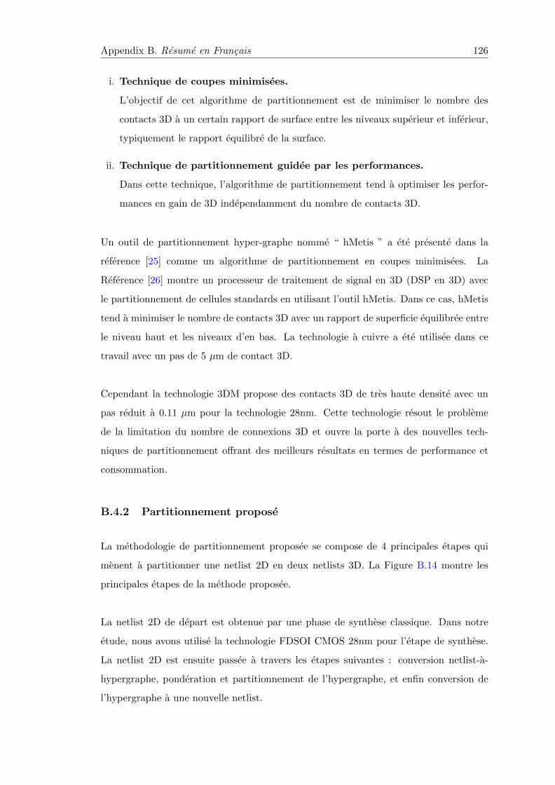
Appendix B. Resume en Francais 126
i. Technique de coupes minimisees.
L’objectif de cet algorithme de partitionnement est de minimiser le nombre des
contacts 3D a un certain rapport de surface entre les niveaux superieur et inferieur,
typiquement le rapport equilibre de la surface.
ii. Technique de partitionnement guidee par les performances.
Dans cette technique, l’algorithme de partitionnement tend a optimiser les perfor-
mances en gain de 3D independamment du nombre de contacts 3D.
Un outil de partitionnement hyper-graphe nomme “ hMetis ” a ete presente dans la
reference [25] comme un algorithme de partitionnement en coupes minimisees. La
Reference [26] montre un processeur de traitement de signal en 3D (DSP en 3D) avec
le partitionnement de cellules standards en utilisant l’outil hMetis. Dans ce cas, hMetis
tend a minimiser le nombre de contacts 3D avec un rapport de superficie equilibree entre
le niveau haut et les niveaux d’en bas. La technologie a cuivre a ete utilisee dans ce
travail avec un pas de 5 µm de contact 3D.
Cependant la technologie 3DM propose des contacts 3D de tres haute densite avec un
pas reduit a 0.11 µm pour la technologie 28nm. Cette technologie resout le probleme
de la limitation du nombre de connexions 3D et ouvre la porte a des nouvelles tech-
niques de partitionnement offrant des meilleurs resultats en termes de performance et
consommation.
B.4.2 Partitionnement propose
La methodologie de partitionnement proposee se compose de 4 principales etapes qui
menent a partitionner une netlist 2D en deux netlists 3D. La Figure B.14 montre les
principales etapes de la methode proposee.
La netlist 2D de depart est obtenue par une phase de synthese classique. Dans notre
etude, nous avons utilise la technologie FDSOI CMOS 28nm pour l’etape de synthese.
La netlist 2D est ensuite passee a travers les etapes suivantes : conversion netlist-a-
hypergraphe, ponderation et partitionnement de l’hypergraphe, et enfin conversion de
l’hypergraphe a une nouvelle netlist.
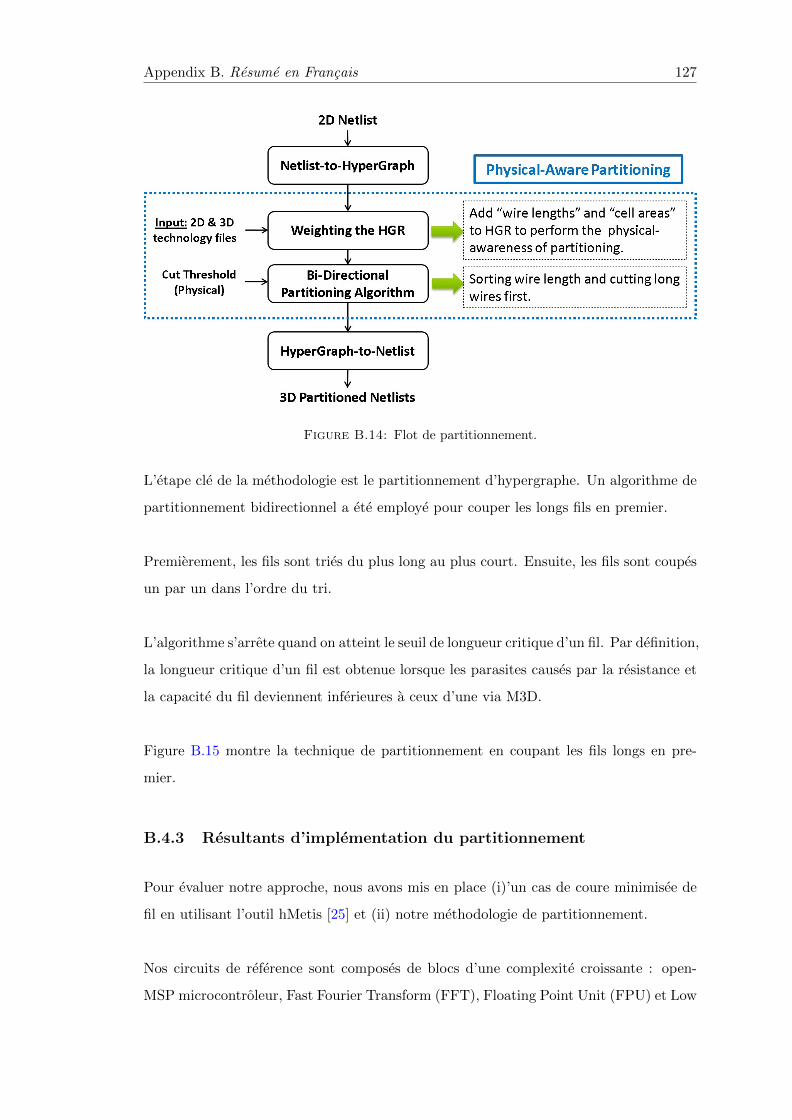
Appendix B. Resume en Francais 127
Figure B.14: Flot de partitionnement.
L’etape cle de la methodologie est le partitionnement d’hypergraphe. Un algorithme de
partitionnement bidirectionnel a ete employe pour couper les longs fils en premier.
Premierement, les fils sont tries du plus long au plus court. Ensuite, les fils sont coupes
un par un dans l’ordre du tri.
L’algorithme s’arrete quand on atteint le seuil de longueur critique d’un fil. Par definition,
la longueur critique d’un fil est obtenue lorsque les parasites causes par la resistance et
la capacite du fil deviennent inferieures a ceux d’une via M3D.
Figure B.15 montre la technique de partitionnement en coupant les fils longs en pre-
mier.
B.4.3 Resultants d’implementation du partitionnement
Pour evaluer notre approche, nous avons mis en place (i)’un cas de coure minimisee de
fil en utilisant l’outil hMetis [25] et (ii) notre methodologie de partitionnement.
Nos circuits de reference sont composes de blocs d’une complexite croissante : open-
MSP microcontroleur, Fast Fourier Transform (FFT), Floating Point Unit (FPU) et Low
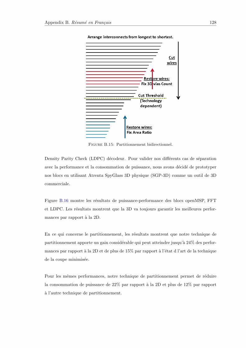
Appendix B. Resume en Francais 128
Figure B.15: Partitionnement bidirectionnel.
Density Parity Check (LDPC) decodeur. Pour valider nos differents cas de separation
avec la performance et la consommation de puissance, nous avons decide de prototyper
nos blocs en utilisant Atrenta SpyGlass 3D physique (SGP-3D) comme un outil de 3D
commerciale.
Figure B.16 montre les resultats de puissance-performance des blocs openMSP, FFT
et LDPC. Les resultats montrent que la 3D va toujours garantir les meilleures perfor-
mances par rapport a la 2D.
En ce qui concerne le partitionnement, les resultats montrent que notre technique de
partitionnement apporte un gain considerable qui peut atteindre jusqu’a 24% des perfor-
mances par rapport a la 2D et de plus de 15% par rapport a l’etat d l’art de la technique
de la coupe minimisee.
Pour les memes performances, notre technique de partitionnement permet de reduire
la consommation de puissance de 22% par rapport a la 2D et plus de 12% par rapport
a l’autre technique de partitionnement.
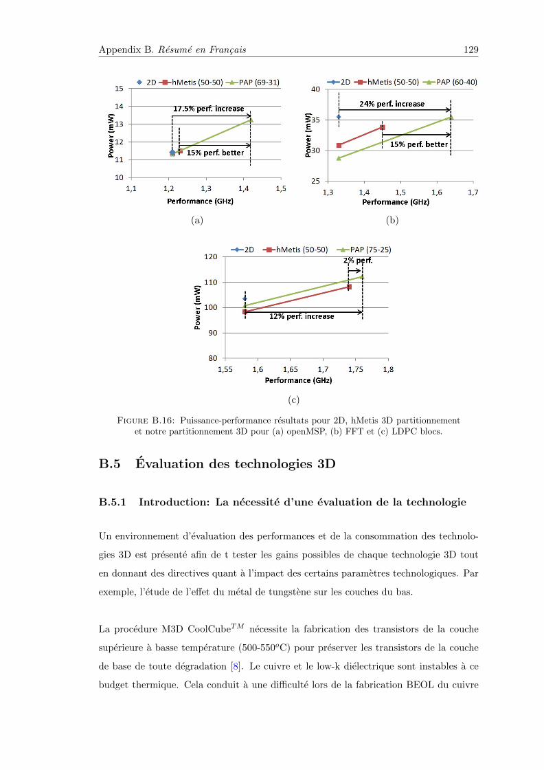
Appendix B. Resume en Francais 129
(a) (b)
(c)
Figure B.16: Puissance-performance resultats pour 2D, hMetis 3D partitionnementet notre partitionnement 3D pour (a) openMSP, (b) FFT et (c) LDPC blocs.
B.5 Evaluation des technologies 3D
B.5.1 Introduction: La necessite d’une evaluation de la technologie
Un environnement d’evaluation des performances et de la consommation des technolo-
gies 3D est presente afin de t tester les gains possibles de chaque technologie 3D tout
en donnant des directives quant a l’impact des certains parametres technologiques. Par
exemple, l’etude de l’effet du metal de tungstene sur les couches du bas.
La procedure M3D CoolCubeTM necessite la fabrication des transistors de la couche
superieure a basse temperature (500-550oC) pour preserver les transistors de la couche
de base de toute degradation [8]. Le cuivre et le low-k dielectrique sont instables a ce
budget thermique. Cela conduit a une difficulte lors de la fabrication BEOL du cuivre
Appendix B. Resume en Francais 130
et du low-k dielectrique de la couche du bas. Une solution simple serait d’utiliser SiO2
avec des lignes de tungstene (W) qui sont stables a un budget thermique superieur.
Dans notre etude, l’effet de W/SiO2 est egal a 6x la resistivite et 1.6x la capacite du
cuivre et du low-k dielectrique [8, 55], d’ou n l’interet d’etudier cet effet au niveau de la
conception.
B.5.2 Evaluation et resultats
L’implementation physique se fait en 2D et en 3D avec l’extraction du cuivre BEOL selon
le flot d’evaluation introduit au chapitre precedent. Nous extrayons le fichier SPEF qui
contient tous les parasites au niveau de las la conception. Ensuite, l’effet W/SiO2 est
appliquee en mettant a jour le fichier SPEF avec les valeurs de la resistivite et de la
capacite relatives au W/SiO2. La section suivante se concentre sur la mise a jour du
fichier des parasites avec du tungstene (W/SiO2).
La figure B.17 montre les resultats de puissance-performance pour les blocs FFT, FPU et
LDPC en utilisant differentes I-BEOL pour les implementations 3D. La degradation des
performances et l’augmentation de la puissance sont presentees de Cu/low-k a W/SiO2
en raison de l’augmentation de la resistance et de la capacite parasites de la W/SiO2.
Les resultats de la puissance et de la performance montrent un effet limite du tungstene
W/SiO2 BEOL par rapport au cuivre Cu/low-k I-BEOL ; au-dessous de 2% des per-
formances se degradent, et en dessous de 1.5% la puissance augmente. Ces resultats
sont en fonction de la complexite des blocs, du partitionnement utilise, du cadre de
l’implementation physique et du nœud technologique CMOS utilise.
B.6 Conclusion
L’impact des interconnexions d’un circuit integre sur les performances et la consomma-
tion est de plus en plus important a partir du nœud CMOS 28 nm et au-dela, ayant
pour effet de reduire les effets benefiques de la loi de Moore. Cela a motive l’interet
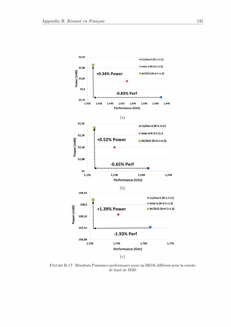
Appendix B. Resume en Francais 131
(a)
(b)
(c)
Figure B.17: Resultats Puissance-performance pour un BEOL different pour la couchede fond de M3D
Appendix B. Resume en Francais 132
des technologies d’empilement 3D pour reduire l’effet des interconnexions sur les per-
formances des circuits. Les technologies d’empilement 3D varient suivant differents
procedes de fabrication d’ou l’on mettra en avant la technologie Through-Silicon-Via
(TSV) - Collage Cuivre-Cuivre (Cu-Cu) et 3D Monolithique. TSV et Cu-Cu presentent
des diametres d’interconnexions 3D de l’ordre de 10 µm tandis que le diametre d’une
interconnexion 3D Monolithique est 0.1 µm, c’est-a-dire cent fois plus petit. Un tel
diametre d’interconnexion creee de nouveaux challenges en matiere de conception de
circuits integres numerique.
Trois contributions principales constituent cette these :
La densite d’integration offerte par les technologies d’empilement etudiees laisse la pos-
sibilite de revoir la topologie des cellules de base en les concevant directement en 3D.
C’est ce qui a ete fait dans l’approche Cellule sur Amplificateur (Cell-on-Buffer – CoB),
en empilant la fonction logique d’une cellule sur l’etage d’amplification. Les simulations
montrent des gains substantiels par rapport aux circuits 2D. On a imagine par la suite
desaligner les niveaux d’alimentation de chaque tranche afin de creer une technique de
Multi-VDD adaptee a l’empilement 3D pour reduire encore plus la consommation des
circuits 3D. Dans un deuxieme temps, le partitionnement grain fin des cellules a ete
etudie. En effet au niveau VLSI, quand on concoit un circuit de plusieurs milliers voire
million de cellules standard en 3D, se pose la question de l’attribution de telle ou telle
cellule sur la tranche haute ou basse du circuit 3D afin d’accroitre au mieux les perfor-
mances et consommation du circuit 3D. Une methodologie de partitionnement physique
est introduite pour cela. Enfin un environnement d’evaluation des performances et con-
sommation des technologies 3D est presente avec pour objectif de rapidement tester les
gains possibles de chaque technologie 3D tout en donnant des directives quant a l’impact
des certains parametres technologiques sur les performances et la consommation.
List of Publications
Patents:
1. Hossam Sarhan, Olivier Billoint, Fabien clermidy, Sebastien Thuries. 2014. 3D
Circuit Design Method. FRANCE. No E.N.: 14 60962. Filing date 13/11/2014.
Conference Papers:
2. H. Sarhan, S. Thuries, O. Billoint, F. Clermidy, “3DCoB: A new design ap-
proach for Monolithic 3D Integrated Circuits”, Asia and South Pacific Design
Automation Conference (ASP-DAC), IEEE, 2014.
3. H. Sarhan, S. Thuries, O. Billoint, F. Clermidy, “An Un-Balanced Area Ratio
Study for High Performance Monolithic 3D Integrated Circuits”, ISVLSI,
IEEE Computer Society Annual Symposium on. (ISVLSI), 2015.
4. H. Sarhan, S. Thuries, O. Billoint, F. Clermidy, “A Power-Performance Study
For Monolithic 3D Integrated Circuit Design Using Un-Balanced Area
Ratio Approach”, Design Automation Conference, Work in Progress session (DAC,
WIP), 2015.
5. H. Sarhan, S. Thuries, O. Billoint, F. Depart, A. Sousa, P. Batude, C. Fenouillet-
Beranger, F. Clermidy, “Intermediate BEOL process influence on Power and
Performance For 3DVLSI”, 3D System Integration, 2015. (3DIC). IEEE Inter-
national Conference on. IEEE, 2015.
133
List of Publications 134
6. O. Billoint, H. Sarhan, Iyad Rayane, M. Vinet, P. Batude, et al., “A Comprehen-
sive Study of Monolithic 3D Cell on Cell Design Using Commercial 2D
Tool”, Design Automation and Test in Europe (DATE), 2015.
7. O. Billoint, H. Sarhan, Iyad Rayane, M. Vinet, P. Batude, et al., “From 2D to
Monolithic 3D: Design Possibilities, Expectations and Challenges”, Pro-
ceedings of the 2015 Symposium on International Symposium on Physical Design,
(ISPD) ACM, 2015.
8. F. Clermidy, O. Billoint, H. Sarhan, S. Thuries, “Technology scaling: the Cool-
Cube TM paradigm”, SOI-3D-Subthreshold Microelectronics Technology Unified
Conference (S3S), IEEE ,2015.
9. B. Boguslawski, H. Sarhan, F. Heitzmann, F. Seguin, S. Thuries, O. Billoint, F.
Clermidy, “Compact Interconnect Approach for Networks of Neural Cliques
Using 3D Technology”, Proceedings of the IFIP/IEEE International Conference
on Very Large Scale Integration (VLSI-SoC), 2015.
10. Batude, P.; Fenouillet-Beranger, C.; Pasini, L.; Lu, V.; Deprat, F.; Brunet, L.; Skle-
nard, B.; Piegas-Luce, F.; Casse, M.; Mathieu, B.; Billoint, O.; Cibrario, G.; Turky-
ilmaz, O.; Sarhan, H.; Thuries, S.; Hutin, L.; Sollier, S.; Widiez, J.; Hortemel,
L.; Tabone, C.; Samson, M-P; Previtali, B.; Rambal, N.; Ponthenier, F.; Mazurier,
J.; Beneyton, R.; Bidaud, M.; Josse, E.; Petitprez, E.; Rozeau, O.; Rivoire, M.;
Euvard-Colnat, C.; Seignard, A.; Fournel, F.; Benaissa, L.; Coudrain, P.; Leduc,
P.; Hartmann, J-M.; Besson, P.; Kerdiles, S.; Bout, C.; Nemouchi, F.; Royer, A.;
Agraffeil, C.; Ghibaudo, G.; Signamarcheix, T.; Haond, M.; Clermidy, F.; Faynot,
O.; Vinet, M., “3DVLSI with CoolCube process: An alternative path to
scaling,” in VLSI Technology (VLSI Technology), 2015 Symposium on , vol., no.,
pp.T48-T49, 16-18 June 2015.
11. Batude, P.; Sklenard, B.; Fenouillet-Beranger, C.; Previtali, B.; Tabone, C.; Rozeau,
O.; Billoint, O.; Turkyilmaz, O.; Sarhan, H.; Thuries, S.; Cibrario, G.; Brunet, L.;
Deprat, F.; Michallet, J.-E.; Clermidy, F.; Vinet, M., ”3D sequential integration
opportunities and technology optimization,” in Interconnect Technology Con-
ference / Advanced Metallization Conference (IITC/AMC), 2014 IEEE International
, vol., no., pp.373-376, 20-23 May 2014.

List of Publications 135
12. Vinet, M.; Batude, P.; Fenouillet-Beranger, C.; Clermidy, F.; Brunet, L.; Rozeau,
O.; Hartmannn, J.; Billoint, O.; Cibrario, G.; Previtali, B.; Tabone, C.; Sklenard,
B.; Turkyilmaz, O.; Ponthenier, F.; Rambal, N.; Samson, M.; Deprat, F.; Lu, V.;
Pasini, L.; Thuries, S.; Sarhan, H.; Michallet, J.-E.; Faynot, O., “Monolithic
3D integration: A powerful alternative to classical 2D scaling,” in SOI-
3D-Subthreshold Microelectronics Technology Unified Conference (S3S), 2014 IEEE
, vol., no., pp.1-3, 6-9 Oct. 2014.
Bibliography
[1] Semiconductor Industry Association. “The International Technology Roadmap for
Semiconductors (ITRS)”. 2011 Edition.
[2] Gordon E Moore et al. Cramming More Components onto Integrated Circuits.
Proceedings of the IEEE, 86(1):82–85, 1998.
[3] Wolfgang Arden, Michel Brillouet, Patrick Cogez, Mart Graef, Bert Huizing, and
Reinhard Mahnkopf. Morethan-Moore white paper.
[4] Geoffrey Yeap. Smart mobile socs driving the semiconductor industry: Technology
trend, challenges and opportunities. In Electron Devices Meeting (IEDM), 2013
IEEE International, pages 1–3. IEEE, 2013.
[5] Tezzaron Semiconductor. 2013.
[6] Hamed Chaabouni, M Rousseau, P Leduc, A Farcy, R El Farhane, Aurelie Thuaire,
G Haury, A Valentian, G Billiot, M Assous, et al. Investigation on TSV impact
on 65nm CMOS devices and circuits. In Electron Devices Meeting (IEDM), 2010
IEEE International, pages 35–1. IEEE, 2010.
[7] L Sanchez, L Bally, B Montmayeul, F Fournel, J Dafonseca, E Augendre, L Di
Cioccio, V Carron, T Signamarcheix, R Taibi, et al. Chip to wafer direct bond-
ing technologies for high density 3D integration. In Electronic Components and
Technology Conference (ECTC), 2012 IEEE 62nd, pages 1960–1964. IEEE, 2012.
[8] P Batude, C Fenouillet-Beranger, L Pasini, V Lu, F Deprat, L Brunet, B Sklenard,
F Piegas-Luce, M Casse, B Mathieu, et al. 3DVLSI with CoolCube process: An al-
ternative path to scaling. In VLSI Technology (VLSI Technology), 2015 Symposium
on, pages T48–T49. IEEE, 2015.
136
Bibliography 137
[9] M Vinet, P Batude, C Fenouillet-Beranger, F Clermidy, L Brunet, O Rozeau,
J Hartmannn, O Billoint, G Cibrario, B Previtali, et al. Monolithic 3d integra-
tion: a powerful alternative to classical 2d scaling. In SOI-3D-Subthreshold Mi-
croelectronics Technology Unified Conference (S3S), 2014 IEEE, pages 1–3. IEEE,
2014.
[10] Denis Dutoit, Christian Bernard, Severine Cheramy, Fabien Clermidy, Yvain Thon-
nart, Pascal Vivet, Christian Freund, Vincent Guerin, Stephane Guilhot, Stephane
Lecomte, et al. A 0.9 pJ/bit, 12.8 GByte/s WideIO memory interface in a 3D-
IC NoC-based MPSoC. In VLSI Technology (VLSIT), 2013 Symposium on, pages
C22–C23. IEEE, 2013.
[11] Matt Wordeman, Joel Silberman, Gary Maier, and Michael Scheuermann. A 3D sys-
tem prototype of an eDRAM cache stacked over processor-like logic using through-
silicon vias. In Solid-State Circuits Conference Digest of Technical Papers (ISSCC),
2012 IEEE International, pages 186–187. IEEE, 2012.
[12] S.W. Ho, Mian Zhi Ding, Pei Siang Lim, D.I. Cereno, G. Katti, Tai Chong Chai, and
S. Bhattacharya. 2.5D through silicon interposer package fabrication by chip-on-
wafer (CoW) approach. In Electronics Packaging Technology Conference (EPTC),
2014 IEEE 16th, pages 679–683, Dec 2014. doi: 10.1109/EPTC.2014.7028352.
[13] B. Patti. Implementing 2.5D and 3D Devices. In AIDA workshop. Tezzaron Semi-
conductor.
[14] Hamed Chaabouni, M Rousseau, P Leduc, A Farcy, R El Farhane, Aurelie Thuaire,
G Haury, A Valentian, G Billiot, M Assous, et al. Investigation on TSV impact
on 65nm CMOS devices and circuits. In Electron Devices Meeting (IEDM), 2010
IEEE International, pages 35–1. IEEE, 2010.
[15] P Batude, B Sklenard, C Fenouillet-Beranger, B Previtali, C Tabone, O Rozeau,
O Billoint, O Turkyilmaz, H Sarhan, S Thuries, et al. 3D sequential integration
opportunities and technology optimization. In Interconnect Technology Confer-
ence/Advanced Metallization Conference (IITC/AMC), 2014 IEEE International,
pages 373–376. IEEE, 2014.
Bibliography 138
[16] F Clermidy, O Billoint, H Sarhan, and S Thuries. Technology scaling: The cool-
cube tm paradigm. In SOI-3D-Subthreshold Microelectronics Technology Unified
Conference (S3S), 2015 IEEE, pages 1–4. IEEE, 2015.
[17] Gabriel H Loh, Yuan Xie, and Bryan Black. Processor Design in 3D Die-Stacking
Technologies. Micro, IEEE, 27(3):31–48, 2007.
[18] Matt Wordeman, Joel Silberman, Gary Maier, and Michael Scheuermann. A 3D sys-
tem prototype of an eDRAM cache stacked over processor-like logic using through-
silicon vias. In Solid-State Circuits Conference Digest of Technical Papers (ISSCC),
2012 IEEE International, pages 186–187. IEEE, 2012.
[19] Hideaki Saito, Masayuki Nakajima, Takumi Okamoto, Yusuke Yamada, Akira
Ohuchi, Noriyuki Iguchi, Toshitsugu Sakamoto, Koichi Yamaguchi, and Masayuki
Mizuno. A chip-stacked memory for on-chip SRAM-rich SoCs and processors. Solid-
State Circuits, IEEE Journal of, 45(1):15–22, 2010.
[20] Dae Hyun Kim, Krit Athikulwongse, Michael Healy, Mohammad Hossain, Moon-
gon Jung, Ilya Khorosh, Gokul Kumar, Young-Joon Lee, Dean Lewis, Tzu-Wei
Lin, et al. 3D-MAPS: 3D Massively parallel processor with stacked memory. In
Solid-State Circuits Conference Digest of Technical Papers (ISSCC), 2012 IEEE
International, pages 188–190. IEEE, 2012.
[21] David Fick, Ronald G Dreslinski, Bharan Giridhar, Gyouho Kim, Sangwon Seo,
Matthew Fojtik, Sudhir Satpathy, Yoonmyung Lee, Daeyeon Kim, Nian Liu, et al.
Centip3De: A cluster-based NTC architecture with 64 ARM Cortex-M3 cores in
3D stacked 130 nm CMOS. Solid-State Circuits, IEEE Journal of, 48(1):104–117,
2013.
[22] Geert Van der Plas, Paresh Limaye, Igor Loi, Abdelkarim Mercha, Herman Oprins,
Cristina Torregiani, Steven Thijs, Dimitri Linten, Michele Stucchi, Guruprasad
Katti, et al. Design issues and considerations for low-cost 3-D TSV IC technology.
Solid-State Circuits, IEEE Journal of, 46(1):293–307, 2011.
[23] Ioannis Savidis, Selcuk Kose, and Eby G Friedman. Power noise in tsv-based 3-d
integrated circuits. Solid-State Circuits, IEEE Journal of, 48(2):587–597, 2013.
[24] Moongon Jung, Taigon Song, Yang Wan, Young-Joon Lee, Debabrata Mohapatra,
Hong Wang, Gareth Taylor, Devang Jariwala, Vijay Pitchumani, Philip Morrow,
Bibliography 139
et al. How to reduce power in 3D IC designs: A case study with OpenSPARC T2
core. In Custom Integrated Circuits Conference (CICC), 2013 IEEE, pages 1–4.
IEEE, 2013.
[25] George Karypis, Rajat Aggarwal, Vipin Kumar, and Shashi Shekhar. Multilevel
hypergraph partitioning: applications in VLSI domain. Very Large Scale Integration
(VLSI) Systems, IEEE Transactions on, 7(1):69–79, 1999.
[26] T. Thorolfsson, S. Lipa, and P.D. Franzon. A 10.35 mW/GFlop stacked SAR DSP
unit using fine-grain partitioned 3D integration. In Custom Integrated Circuits
Conference (CICC), 2012 IEEE, pages 1–4, Sept 2012. doi: 10.1109/CICC.2012.
6330589.
[27] Shreepad Panth, Kambiz Samadi, Yang Du, and Sung Kyu Lim. Placement-driven
partitioning for congestion mitigation in monolithic 3D IC designs. Computer-Aided
Design of Integrated Circuits and Systems, IEEE Transactions on, 34(4):540–553,
2015.
[28] Young-Joon Lee, Patrick Morrow, and Sung Kyu Lim. Ultra high density logic
designs using transistor-level monolithic 3D integration. In Proceedings of the In-
ternational Conference on Computer-Aided Design, pages 539–546. ACM, 2012.
[29] Chang Liu and Sung Kyu Lim. A design tradeoff study with monolithic 3D integra-
tion. In Quality Electronic Design (ISQED), 2012 13th International Symposium
on, pages 529–536. IEEE, 2012.
[30] O Thomas, M Vinet, O Rozeau, P Batude, and A Valentian. Compact 6T SRAM
cell with robust Read/Write stabilizing design in 45nm Monolithic 3D IC technol-
ogy. In IC Design and Technology, 2009. ICICDT’09. IEEE International Confer-
ence on, pages 195–198. IEEE, 2009.
[31] Chang Liu and Sung Kyu Lim. Ultra-high density 3D SRAM cell designs for mono-
lithic 3D integration. In IEEE International Interconnect Technology Conference,
pages 1–3, 2012.
[32] Yuan Xie. Processor architecture design using 3D integration technology. In VLSI
Design, 2010. VLSID’10. 23rd International Conference on, pages 446–451. IEEE,
2010.
Bibliography 140
[33] Amr G Wassal, Hossam H Sarhan, and Amr ElSherief. Novel 3D memory-centric
NoC architecture for transaction-based SoC applications. In Electronics, Commu-
nications and Photonics Conference (SIECPC), 2011 Saudi International, pages
1–5. IEEE, 2011.
[34] Jubee Tada, Ryusuke Egawa, Kazushige Kawai, Hiroaki Kobayashi, and Gensuke
Goto. A middle-grain circuit partitioning strategy for 3-D integrated floating-point
multipliers. In 3D Systems Integration Conference (3DIC), 2011 IEEE Interna-
tional, pages 1–6. IEEE, 2012.
[35] Shreepad Panth, Kambiz Samadi, Yang Du, and Sung Kyu Lim. Power-performance
study of block-level monolithic 3D-ICs considering inter-tier performance variations.
In Design Automation Conference (DAC), 2014 51st ACM/EDAC/IEEE, pages 1–
6. IEEE, 2014.
[36] Guojie Luo, Yiyu Shi, and Jason Cong. An Analytical Placement Framework for
3-D ICs and Its Extension on Thermal Awareness. Computer-Aided Design of
Integrated Circuits and Systems, IEEE Transactions on, 32(4):510–523, 2013.
[37] Jason Cong and Guojie Luo. A multilevel analytical placement for 3D ICs. In
Proceedings of the 2009 Asia and South Pacific Design Automation Conference,
pages 361–366. IEEE Press, 2009.
[38] Meng-Kai Hsu, Yao-Wen Chang, and Valeriy Balabanov. TSV-aware analytical
placement for 3D IC designs. In Design Automation Conference (DAC), 2011 48th
ACM/EDAC/IEEE, pages 664–669. IEEE, 2011.
[39] Shashikanth Bobba, Ashutosh Chakraborty, Olivier Thomas, Perrine Batude,
Thomas Ernst, Olivier Faynot, David Z Pan, and Giovanni De Micheli. CELON-
CEL: Effective design technique for 3-D monolithic integration targeting high per-
formance integrated circuits. In Proceedings of the 16th Asia and South Pacific
Design Automation Conference, pages 336–343. IEEE Press, 2011.
[40] Jason Cong, Guojie Luo, Jie Wei, and Yan Zhang. Thermal-aware 3D IC placement
via transformation. In Design Automation Conference, 2007. ASP-DAC’07. Asia
and South Pacific, pages 780–785. IEEE, 2007.
[41] Xin Zhao, J. Minz, and Sung Kyu Lim. Low-Power and Reliable Clock Network
Design for Through-Silicon Via (TSV) Based 3D ICs. Components, Packaging and
Bibliography 141
Manufacturing Technology, IEEE Transactions on, 1(2):247–259, Feb 2011. ISSN
2156-3950. doi: 10.1109/TCPMT.2010.2099590.
[42] Tak-Yung Kim and Taewhan Kim. Resource allocation and design techniques of
prebond testable 3-D clock tree. Computer-Aided Design of Integrated Circuits and
Systems, IEEE Transactions on, 32(1):138–151, 2013.
[43] Xin Zhao, Jacob Minz, and Sung Kyu Lim. Low-power and reliable clock network
design for through-silicon via (TSV) based 3D ICs. Components, Packaging and
Manufacturing Technology, IEEE Transactions on, 1(2):247–259, 2011.
[44] Liang-Teck Pang, Phillip J Restle, Matthew R Wordeman, Joel A Silberman,
Robert L Franch, and Gary W Maier. A shorted global clock design for multi-
GHz 3D stacked chips. In 2012 Symposium on VLSI Circuits (VLSIC), 2012.
[45] Vasilis F Pavlidis, Ioannis Savidis, and EbyG Friedman. Clock distribution networks
for 3-D ictegrated Circuits. In Custom Integrated Circuits Conference, 2008. CICC
2008. IEEE, pages 651–654. IEEE, 2008.
[46] Yuan Xie, Jason Cong, and Sachin S Sapatnekar. Three-dimensional integrated
circuit design. Springer, 2010.
[47] O Billoint, H Sarhan, I Rayane, M Vinet, P Batude, C Fenouillet-Beranger,
O Rozeau, G Cibrario, F Deprat, A Fustier, et al. A comprehensive study of mono-
lithic 3D cell on cell design using commercial 2D tool. In Proceedings of the 2015
Design, Automation & Test in Europe Conference & Exhibition, pages 1192–1196.
EDA Consortium, 2015.
[48] Atrenta Inc. www.atrenta.com.
[49] Kihwan Choi, Ramakrishna Soma, and Massoud Pedram. Fine-grained dynamic
voltage and frequency scaling for precise energy and performance tradeoff based on
the ratio of off-chip access to on-chip computation times. Computer-Aided Design
of Integrated Circuits and Systems, IEEE Transactions on, 24(1):18–28, 2005.
[50] John Howard, Saurabh Dighe, Yatin Hoskote, Sriram Vangal, David Finan, Gregory
Ruhl, Devon Jenkins, Howard Wilson, Nitin Borkar, Gerhard Schrom, et al. A 48-
core IA-32 message-passing processor with DVFS in 45nm CMOS. In Solid-State
Bibliography 142
Circuits Conference Digest of Technical Papers (ISSCC), 2010 IEEE International,
pages 108–109. IEEE, 2010.
[51] Hossam Sarhan, Sebastien Thuries, Olivier Billoint, Fabien Deprat, Alexandre
Ayres De Sousa, Perrine Batude, Claire Fenouillet-Beranger, and Fabien Clermidy.
Intermediate BEOL process influence on Power and Performance For 3DVLSI. In
3D Systems Integration Conference (3DIC), 2015 IEEE International. IEEE, 2015.
[52] Kiran Puttaswamy and Gabriel H Loh. Dynamic instruction schedulers in a 3-
dimensional integration technology. In Proceedings of the 16th ACM Great Lakes
symposium on VLSI, pages 153–158. ACM, 2006.
[53] Jason Cong, Guojie Luo, Jie Wei, and Yan Zhang. Thermal-aware 3D IC placement
via transformation. In Design Automation Conference, 2007. ASP-DAC’07. Asia
and South Pacific, pages 780–785. IEEE, 2007.
[54] Yuchun Ma, Yongxiang Liu, Eren Kursun, Glenn Reinman, and Jason Cong. Inves-
tigating the effects of fine-grain three-dimensional integration on microarchitecture
design. ACM Journal on Emerging Technologies in Computing Systems (JETC), 4
(4):17, 2008.
[55] C. Fenouillet-Beranger and et al. W and Copper interconnection stability for 3D
VLSI CoolCube integration. International Conference on Solid State Devices and
Materials (SSDM), 2015.
[56] Hai Wei, Tony F Wu, Deepak Sekar, Brian Cronquist, R Fabian Pease, and Sub-
hasish Mitra. Cooling three-dimensional integrated circuits using power delivery
networks. In Electron Devices Meeting (IEDM), 2012 IEEE International, pages
14–2. IEEE, 2012.
[57] Sandeep Kumar Samal, Kambiz Samadi, Pratyush Kamal, Yun Du, and Sung Kyu
Lim. Full chip impact study of power delivery network designs in monolithic 3d ics.
In Computer-Aided Design (ICCAD), 2014 IEEE/ACM International Conference
on, pages 565–572. IEEE, 2014.
[58] Mehdi Saeidi, Kambiz Samadi, Arpit Mittal, and Rajat Mittal. Thermal implica-
tions of mobile 3d-ics. In 3D Systems Integration Conference (3DIC), 2014 Inter-
national, pages 1–7. IEEE, 2014.
Bibliography 143
[59] Sandeep Kumar Samal, Shreepad Panth, Kambiz Samadi, Mehdi Saedi, Yang Du,
and Sung Kyu Lim. Fast and accurate thermal modeling and optimization for
monolithic 3d ics. In Proceedings of the 51st Annual Design Automation Conference,
pages 1–6. ACM, 2014.
[60] Raul Rojas. Neural Networks: A Systematic Introduction. Springer-Verlag New
York, Inc., New York, NY, USA, 1996. ISBN 3-540-60505-3.
[61] Biswa Sengupta and Martin B. Stemmler. Power consumption during neuronal
computation. Proceedings of the IEEE, 102(5):738–750, 2014. doi: 10.1109/JPROC.
2014.2307755.
[62] Brian Whitworth. Some implications of comparing brain and computer processing.
In HICSS, pages 1–10. IEEE Computer Society, 2008.
[63] Bilel Belhadj, Alexandre Valentian, Pascal Vivet, Marc Duranton, Liqiang He, and
Olivier Temam. The improbable but highly appropriate marriage of 3D stacking
and neuromorphic accelerators. In Proc. CASES’14, pages 1–9, 2014.
[64] Fabien Clermidy et al. Advanced technologies for brain-inspired computing. In
Proc. ASP-DAC’14, 2014.
[65] Vincent Gripon and Claude Berrou. Sparse neural networks with large learning
diversity. 22(7):1087–1096, July 2011.
[66] Norman P. Jouppi. Improving direct-mapped cache performance by the addition of
a small fully-associative cache and prefetch buffers. In ISCA ’90, pages 364–373,
1990.
[67] N.F. Huang et al. Design of multi-field IPv6 packet classifiers using ternary CAMs.
In Proc. IEEE GLOBECOM, volume 3, pages 1877–1881, 2001.
[68] Behrooz Kamary Aliabadi et al. Storing sparse messages in networks of neural
cliques. IEEE Trans. Neural Netw. Learn. Syst., 25(5):980 – 989, 2014.
[69] Benoit Larras, Bartosz Boguslawski, Cyril Lahuec, Matthieu Arzel, Fabrice Seguin,
and Frederic Heitzmann. Analog encoded neural network for power management
in MPSoC. In Proc. NEWCAS’13, pages 1–4, 2013.
Bibliography 144
[70] Wonyoung Kim, Meeta Sharma Gupta, Gu-Yeon Wei, and David Brooks. System
level analysis of fast, per-core DVFS using on-chip switching regulators. In HPCA,
pages 123–134. IEEE Computer Society, 2008.
[71] D.N. Truong et al. A 167-processor computational platform in 65 nm CMOS. 2009.
[72] E. Beigne et al. An asynchronous power aware and adaptive NoC based circuit.
Solid-State Circuits, IEEE Journal of, 44(4):1167–1177, 2009.
[73] B. Larras, B. Boguslawski, C. Lahuec, M. Arzel, F. Seguin, and F. Heitzmann.
Analog encoded neural network for power management in MPSoC. AICSP, 81(3):
595–605, 2014. ISSN 0925-1030.
[74] Fabien Clermidy et al. A 477mW NoC-based digital baseband for mimo 4G SDR.
In ISSCC, pages 278–279. IEEE, 2010. ISBN 978-1-4244-6033-5.
[75] Fabien Clermidy, Romain Lemaire, Xavier Popon, Dimitri Ktenas, and Yvain Thon-
nart. An open and reconfigurable platform for 4G telecommunication: Concepts
and application. In DSD, pages 449–456. IEEE Computer Society, 2009. ISBN
978-0-7695-3782-5.