CHAPITRE 1CHAPITRE 1 - dartec.comdartec.com/MIC4120/CHAP1a.pdf · Dans la jonction p-n, l’excès...
31
CHAPITRE 1 CHAPITRE 1 CHAPITRE 1 CHAPITRE 1 DIODES DIODES Avec la permission de Prentice Hall 1
Transcript of CHAPITRE 1CHAPITRE 1 - dartec.comdartec.com/MIC4120/CHAP1a.pdf · Dans la jonction p-n, l’excès...

CHAPITRE 1CHAPITRE 1CHAPITRE 1CHAPITRE 1
DIODESDIODES
Avec la permission de Prentice Hall
11

DiodesDiodes
La diode est un composant de deux brochesLa diode est un composant de deux broches.
Une diode idéale conduit i t duniquement dans un sens.
22
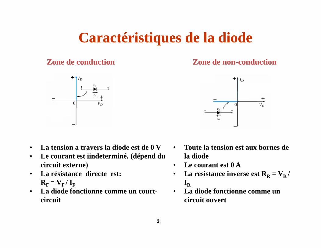
CaractéristiquesCaractéristiques de la diodede la diodeZone de conductionZone de conduction Zone de nonZone de non--conductionconduction
• La tension a travers la diode est de 0 V • Le courant est iindeterminé. (dépend du
circuit externe)é
• Toute la tension est aux bornes de la diode
• Le courant est 0 A• La résistance directe est:
RF = VF / IF• La diode fonctionne comme un court-
circuit
• La resistance inverse est RR = VR / IR
• La diode fonctionne comme un circuit ouvertc cu t c cu t ouve t
33
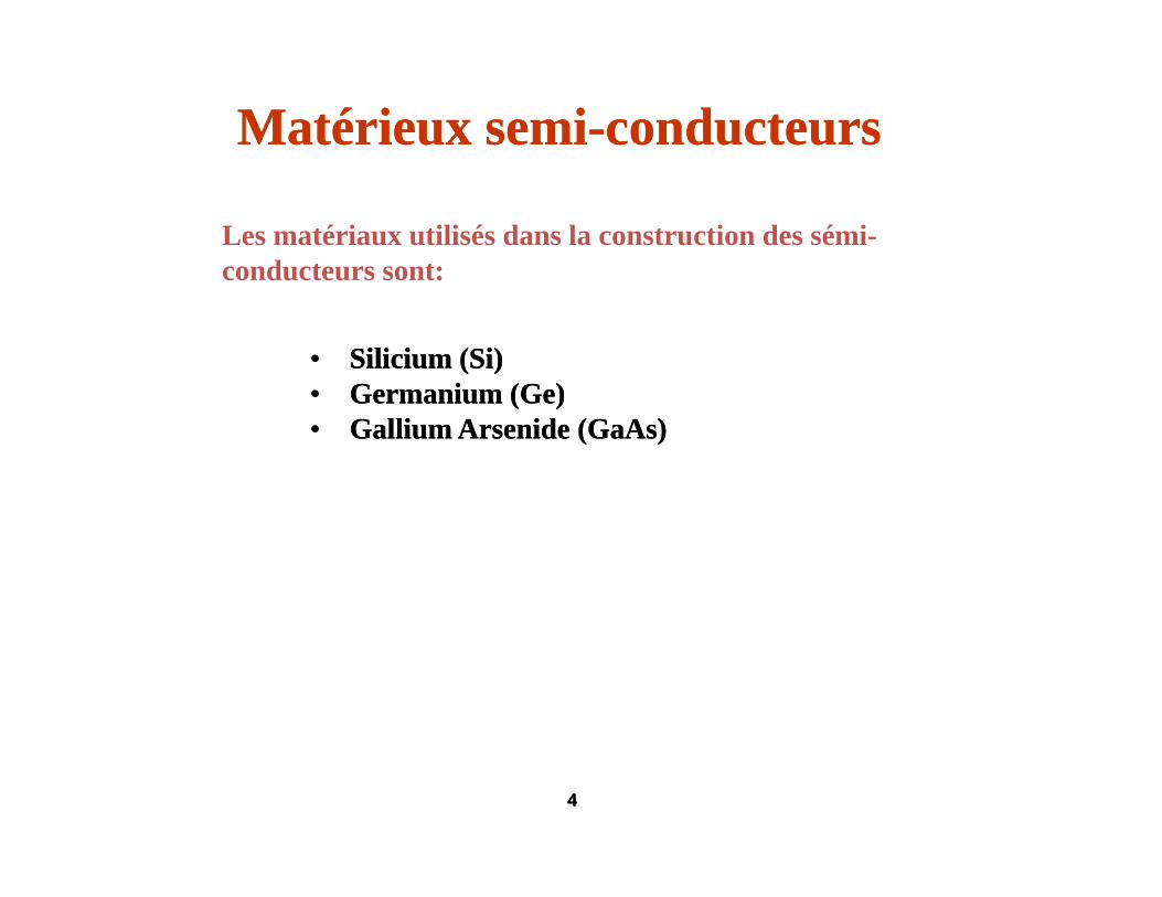
MatérieuxMatérieux semisemi--conducteursconducteurs
Les matériaux utilisés dans la construction des sémi-conducteurs sont:conducteurs sont:
•• SiliciumSilicium (Si)(Si)•• Germanium (Germanium (GeGe))•• Germanium (Germanium (GeGe))•• Gallium Arsenide (Gallium Arsenide (GaAsGaAs))
44
DopageDopage
Les caractéristiques électriqus du silicium et du germanium sontaméliorées en ajoutant des matériaux dans un processus appelédopage.
Il y a deux types de matériau de dopage semi-conducteur:TypeType--nnTypeType--pp
• Le materiau type-n comporte un excès d’electrons.• Le materiau type-p comporte un exceès de trous.
55
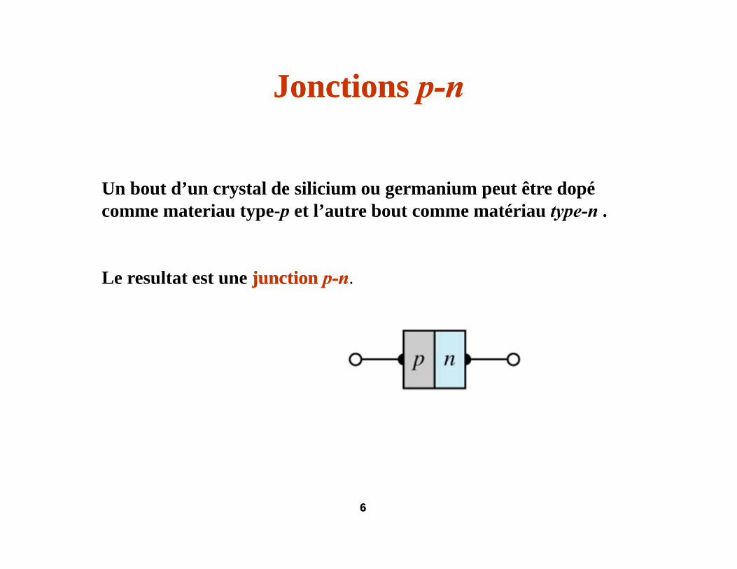
JonctionsJonctions pp--nn
Un bout d’un crystal de silicium ou germanium peut être dopécomme materiau type-p et l’autre bout comme matériau type-n .
Le resultat est une junction junction pp--nn.
66

JonctionsJonctions pp--nnppDans la jonction p-n, l’excèsd’electrons dasn la bande de conduction du cõté de type-n conduction du cõté de type n sont attirés vers les trous du cõtéde type-p.
Th l t i th tThe electrons in the n-type material migrate across the junction to the p-type material (electron flow). ( )
The electron migration results in a negativenegative charge on the p-type side of the junction and a positivepositive
The result is the formation of a depletion regiondepletion region around the junction.
side of the junction and a positivepositivecharge on the n-type side of the junction.
77

Conditions de Conditions de fonctionementfonctionement de la diodede la diode
A diode has three operating conditions:A diode has three operating conditions:
• No bias• Forward bias• Reverse bias
88
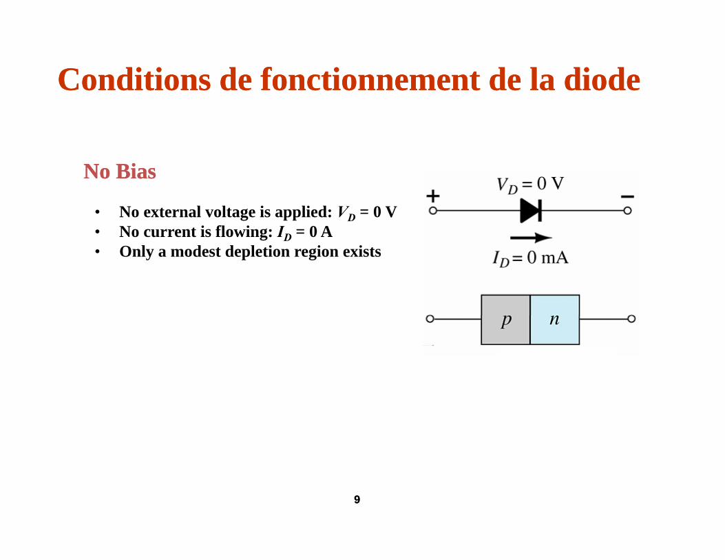
Conditions de Conditions de fonctionnementfonctionnement de la diodede la diode
No BiasNo Bias
• No external voltage is applied: VD = 0 V • No current is flowing: ID = 0 A
No BiasNo Bias
• Only a modest depletion region exists
99
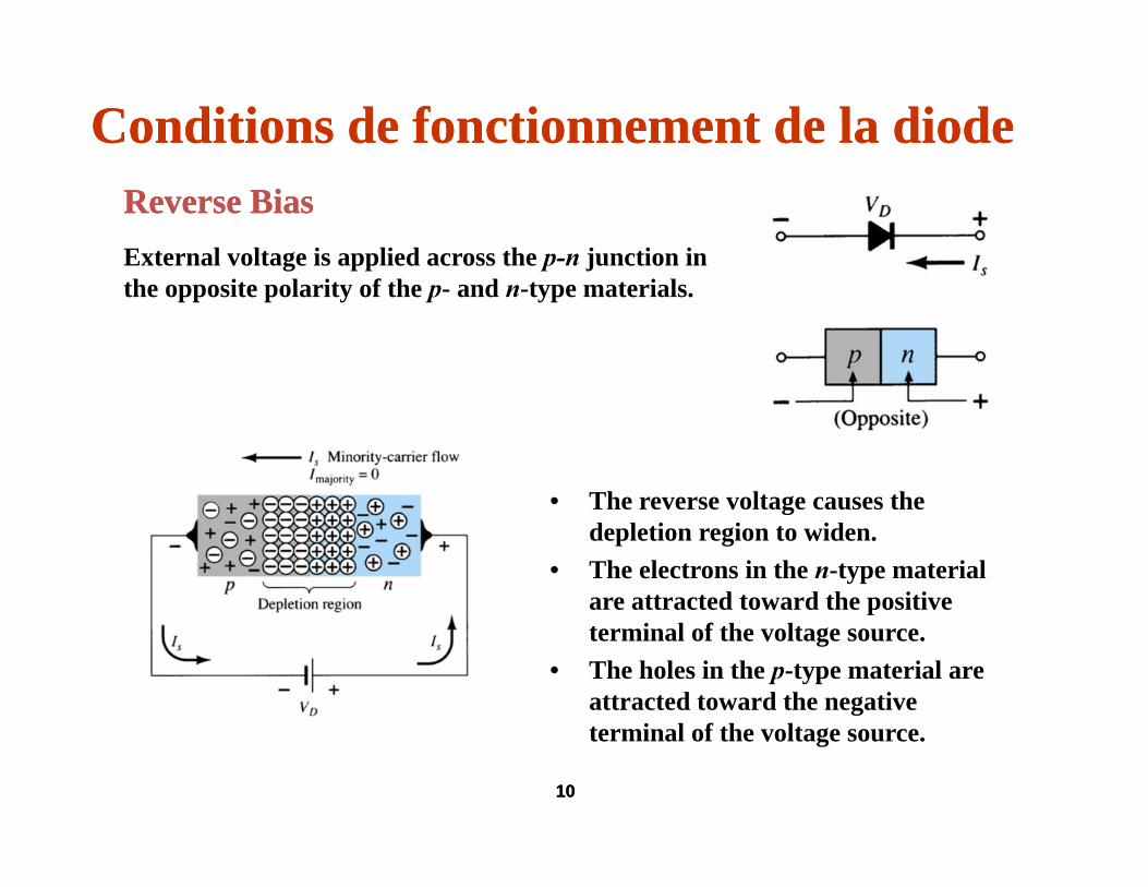
Conditions de Conditions de fonctionnementfonctionnement de la diodede la diode
External voltage is applied across the p-n junction in
Reverse BiasReverse Bias
the opposite polarity of the p- and n-type materials.
• The reverse voltage causes the• The reverse voltage causes the depletion region to widen.
• The electrons in the n-type material are attracted toward the positive pterminal of the voltage source.
• The holes in the p-type material are attracted toward the negative terminal of the voltage source.
1010
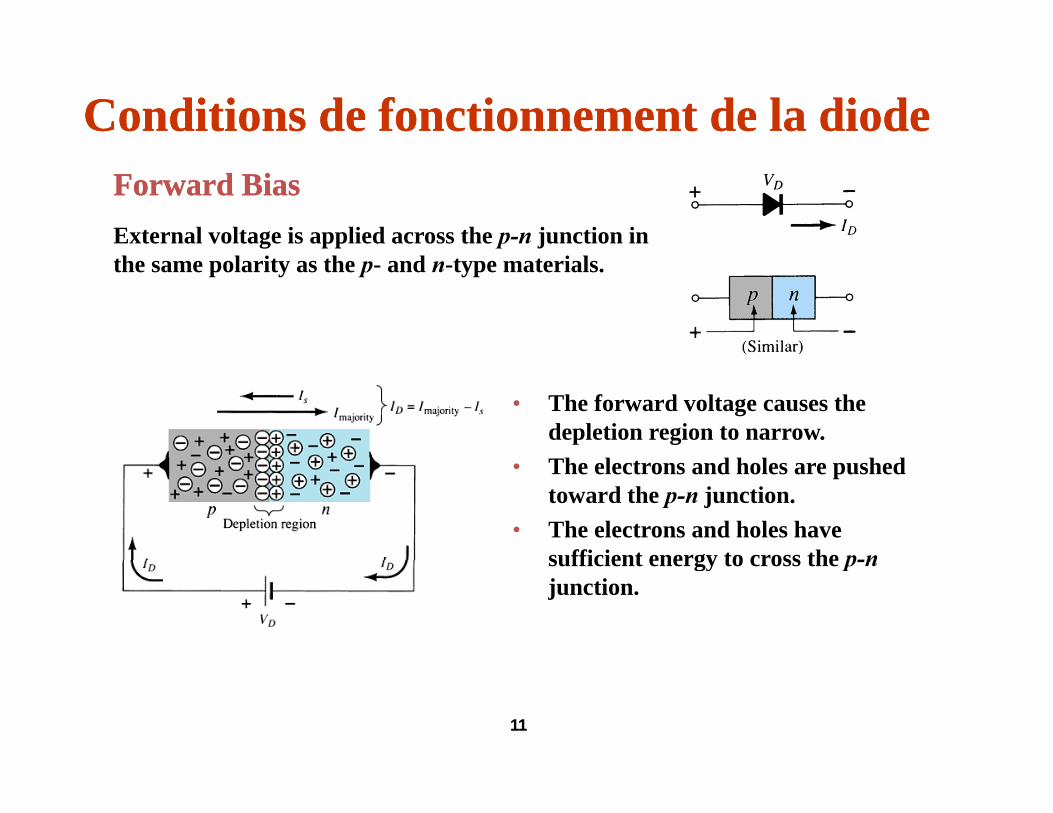
Conditions de Conditions de fonctionnementfonctionnement de la diodede la diodeForward BiasForward BiasExternal voltage is applied across the p-n junction in the same polarity as the p- and n-type materials.
• The forward voltage causes the depletion region to narrow.
• The electrons and holes are pushed toward the p-n junction.
• The electrons and holes have sufficient energy to cross the p-nsufficient energy to cross the p-njunction.
1111
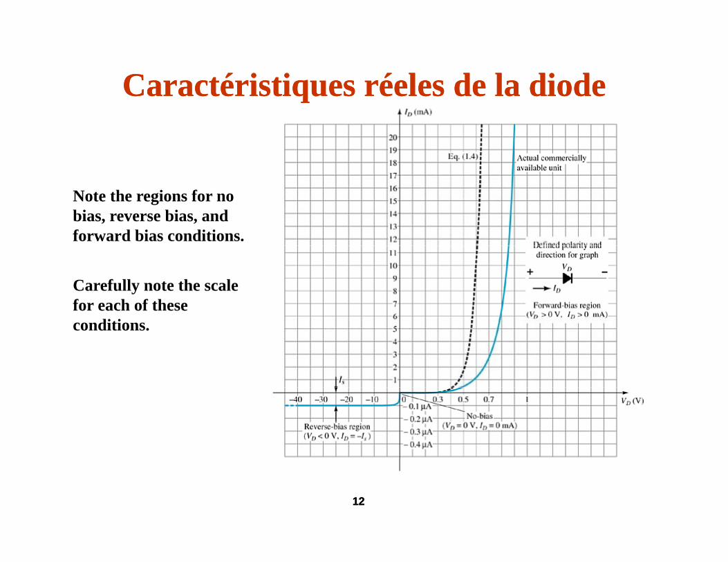
CaractéristiquesCaractéristiques réelesréeles de la diodede la diode
Note the regions for no bias, reverse bias, and forward bias conditions.
Carefully note the scale for each of these conditions.
1212
PortateursPortateurs minoritairesminoritaires et et majoritairesmajoritaires
Two currents through a diode:
Majority CarriersMajority Carriers
• The majority carriers in n type materials are electrons• The majority carriers in n-type materials are electrons.• The majority carriers in p-type materials are holes.
Minority CarriersMinority Carriers
• The minority carriers in n-type materials are holes.The minority carriers in n type materials are holes.• The minority carriers in p-type materials are electrons.
1313
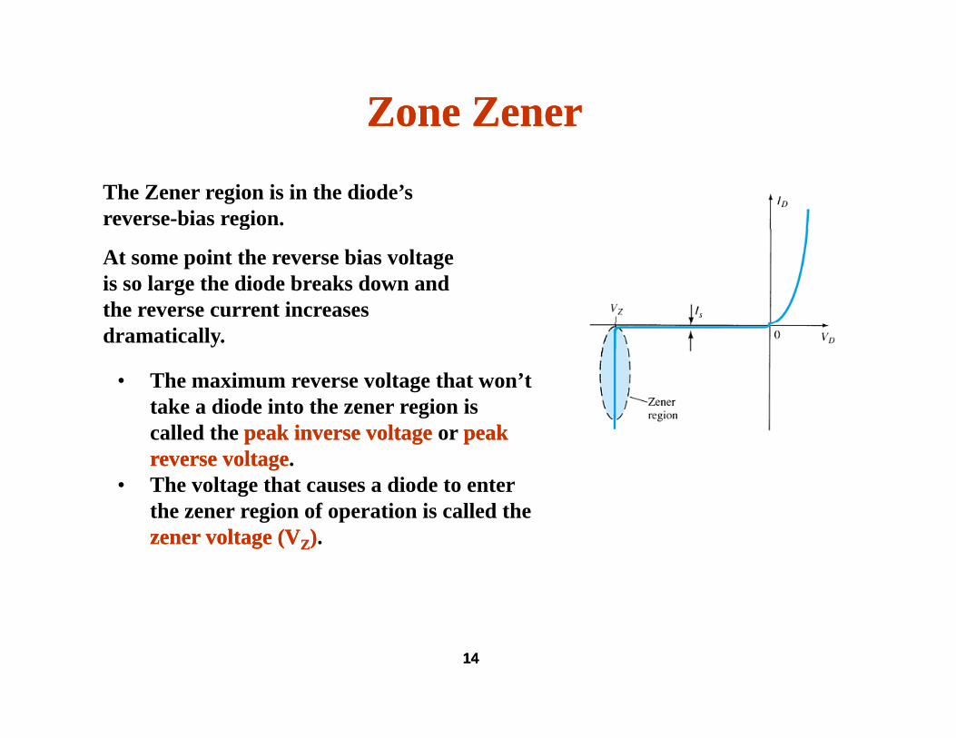
Zone Zone ZenerZener
The Zener region is in the diode’s reverse-bias region.g
At some point the reverse bias voltage is so large the diode breaks down and the reverse current increases dramatically.
• The maximum reverse voltage that won’t take a diode into the zener region is gcalled the peak inverse voltagepeak inverse voltage or peak peak reverse voltagereverse voltage.
• The voltage that causes a diode to enter the zener region of operation is called thethe zener region of operation is called the zener voltage (Vzener voltage (VZZ)).
1414
Tension de Tension de polarisationpolarisation positivepositive
The point at which the diode changes from no-bias condition to forward bias condition occurs when the electrons andto forward-bias condition occurs when the electrons and holes are given sufficient energy to cross the p-n junction. This energy comes from the external voltage applied across the diode.the diode.
The forward bias voltage required for a:
• gallium arsenide diode ≅ 1.2 V• silicon diode ≅ 0.7 V• germanium diode ≅ 0.3 V
1515
EffetEffet de la de la températuretempérature
As temperature increases it adds energy to the diode.
• It reduces the required forward bias voltage for forward-bias conduction.
• It increases the amount of reverse current in the reverse• It increases the amount of reverse current in the reverse-bias condition.
• It increases maximum reverse bias avalanche voltage.
Germanium diodes are more sensitive to temperature variations than silicon or gallium arsenide diodes.
1616
NiveauxNiveaux de résistancede résistance
Semiconductors react differently to DC and AC currents.
There are three types of resistance:
• DC (static) resistance• AC (dynamic) resistance• Average AC resistance Average AC resistance
1717
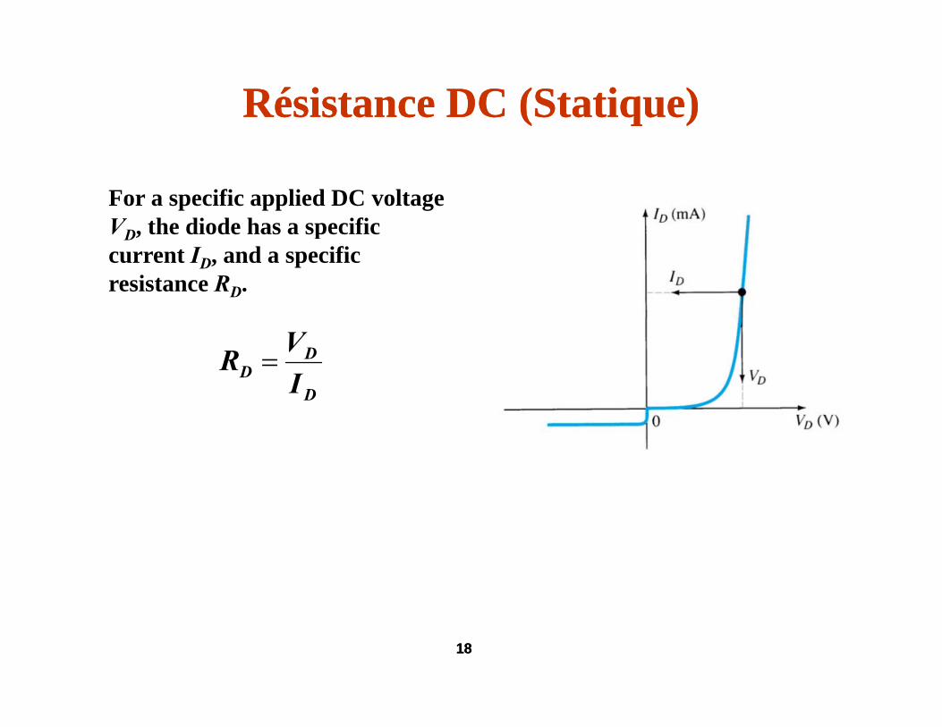
Résistance DC (Résistance DC (StatiqueStatique))
For a specific applied DC voltage V the diode has a specificVD, the diode has a specific current ID, and a specific resistance RD.
D
DD I
VR =
1818
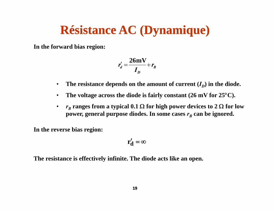
Résistance Résistance AC AC ((DynamiqueDynamique))
rr +=′mV 26
In the forward bias region:
• The resistance depends on the amount of current (ID) in the diode.
BD
d rI
r +=
• The voltage across the diode is fairly constant (26 mV for 25°C).
• rB ranges from a typical 0.1 Ω for high power devices to 2 Ω for low power, general purpose diodes. In some cases rB can be ignored.
∞=′ rd
In the reverse bias region:
d
The resistance is effectively infinite. The diode acts like an open.
1919
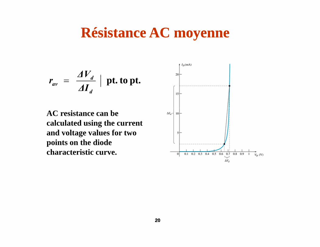
Résistance AC Résistance AC moyennemoyenne
dΔV pt.topt. d
dav ΔI
ΔV r =
AC resistance can be calculated using the current and voltage values for two points on the diode characteristic curve.
2020

Circuit Circuit équivalentéquivalent de la diodede la diode
2121
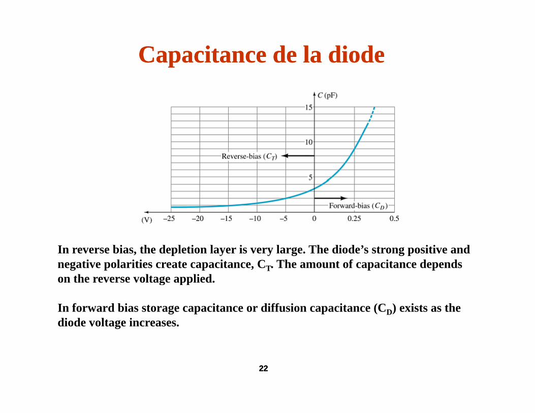
Capacitance de la diodeCapacitance de la diode
In reverse bias, the depletion layer is very large. The diode’s strong positive and negative polarities create capacitance, CT. The amount of capacitance depends on the reverse voltage applied.g pp
In forward bias storage capacitance or diffusion capacitance (CD) exists as the diode voltage increases.
2222
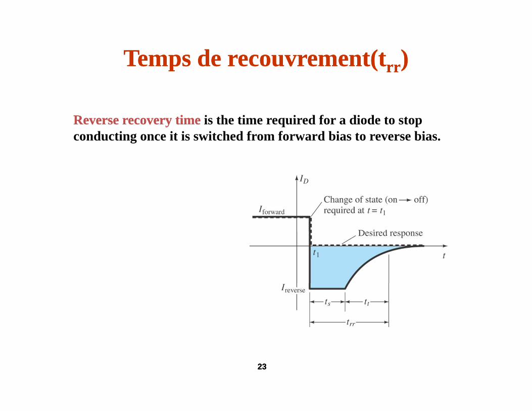
Temps de Temps de recouvrementrecouvrement((ttrrrr))
Reverse recovery timeReverse recovery time is the time required for a diode to stop conducting once it is switched from forward bias to reverse bias.
2323

SpecificationsSpecificationsData about a diode is presented uniformly for many different diodes. This makes cross-matching of diodes for replacement or design easier
1. Forward Voltage (VF) at a specified current and temperature
2. Maximum forward current (IF) at a specified temperature
easier.
F
3. Reverse saturation current (IR) at a specified voltage and temperature
4 Reverse voltage rating PIV or PRV or V(BR) at a specified4. Reverse voltage rating, PIV or PRV or V(BR), at a specified temperature
5. Maximum power dissipation at a specified temperature
6. Capacitance levels
7. Reverse recovery time, trr
8. Operating temperature range8. Operating temperature range
2424
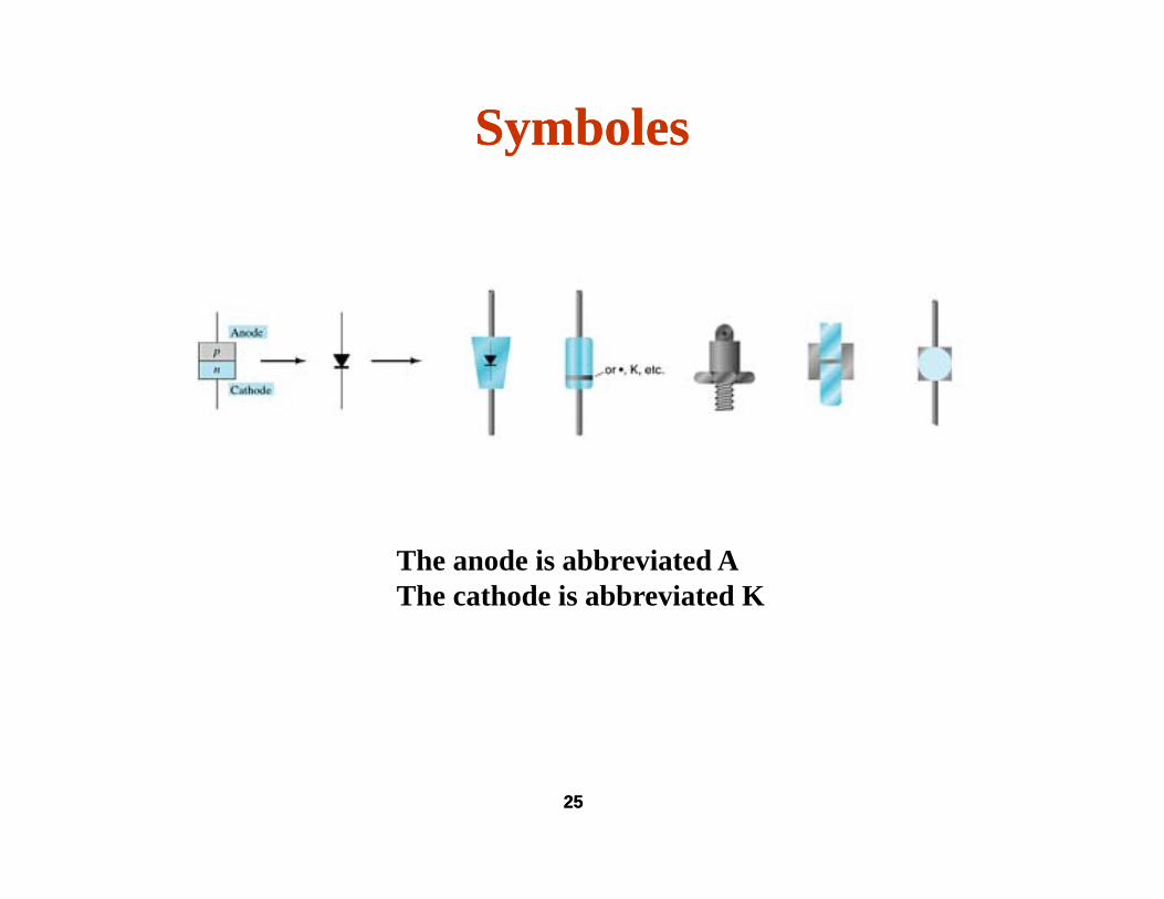
SymbolesSymboles
The anode is abbreviated AThe cathode is abbreviated K
2525

OhmmètreOhmmètre
An ohmmeter set on a low Ohms scale can be used to test a diode. The diode should be tested out of circuit.
2626
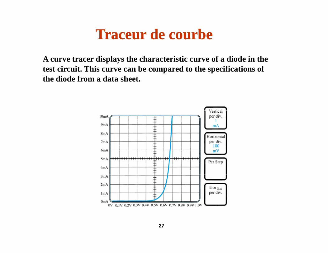
TraceurTraceur de de courbecourbeA curve tracer displays the characteristic curve of a diode in the test circuit. This curve can be compared to the specifications of the diode from a data sheetthe diode from a data sheet.
2727
AutresAutres Types Types de de DiodesDiodes
Zener diodeZener diodeLight-emitting diodeDiode arrays
2828
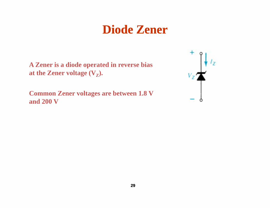
Diode Diode ZenerZener
A Zener is a diode operated in reverse biasA Zener is a diode operated in reverse bias at the Zener voltage (VZ).
C 1 8Common Zener voltages are between 1.8 V and 200 V
2929

Diode ElectroDiode Electro--luminiscentluminiscent (DEL)(DEL)
An LED emits photons when it is forward biased.Th b i h i f d i iblThese can be in the infrared or visible spectrum. The forward bias voltage is usually in the range of 2 V to 3 V.
3030
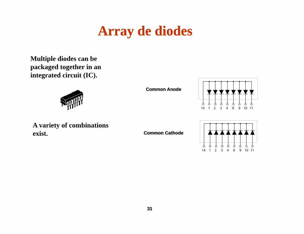
Array Array de diodesde diodes
Multiple diodes can be packaged together in an i i i ( C)integrated circuit (IC).
Common AnodeCommon Anode
C C th dC C th dA variety of combinations
i t Common CathodeCommon Cathodeexist.
3131